Designing Power Inverter with Minimum Harmonic - غزةlibrary.iugaza.edu.ps/thesis/112743.pdf ·...
108
Transcript of Designing Power Inverter with Minimum Harmonic - غزةlibrary.iugaza.edu.ps/thesis/112743.pdf ·...


Designing Power Inverter with Minimum Harmonic
Distortion Using Fuzzy Logic Control
By
Farok Y. Sharaf
Supervisor
Prof. Dr. Mohammed Hussein
This thesis is submitted in Partial Fulfillment of the
Requirements for the Degree of Master of Science in
Electrical Engineering
2014 م – 1435هـ
The Islamic University of Gaza
Research and Graduate Affairs
Faculty of Engineering
Electrical Engineering Department
غــــــــــــزة –الجامعـــة اإلســــــالمية
شؤون البحث العلمي و الدراسات العليـا
كليـــــــــــــــــــة الهندســـــــــــــــــــــة
الكهربائيــــــــةقســـــــــم الهندســــــــة


إقرار
أنا الموقع أدناه مقدم الرسالة التي تحمل العنوان:
.جهاز انفيرتر عالي االداء باستخدام انظمة التحكم الضبابي لتقليل الشوائب تصميم
الخاص، باستثناء ما تمت اإلشارة إليه حيثما قر بأن ما اشتملت عليه هذه الرسالة إنما هي نتاج جهدي أ
ورد، وإن هذه الرسالة ككل، أو أي جزء منها لم يقدم من قبل لنيل درجة أو لقب علمي أو بحثي لدى
أية مؤسسة تعليمية أو بحثية أخرى.
DECLARATION
The work provided in this thesis, unless otherwise referenced, is the
researcher's own work, and has not been submitted elsewhere for any other
degree or qualification.
Student's name: :اسم الطالب
Signature: :التوقيع
Date: :التاريخ

ii
(المناقشة لجنة قبل من الحكم نتيجة) البحث على الحكم نتيجة صفحة

iii
DEDICATION
I would like to dedicate the outcomes of this research thesis to my beloved
father and mother. There is no doubt in my mind that without their continued
support and counsel I could not have completed this process. I also dedicate
this work to all my lovely family members” brothers, sisters, wife, and lovely
kids” who have been a constant source of motivation, inspiration, and
support.
i

iv
Acknowledgement
I thank Allah, the lord of the worlds, for His mercy and limitless help and
guidance. May peace and blessings be upon Mohammed the last of the
messengers.
I would like to express my deep appreciation to my advisor
Prof. Dr. Mohammed Hussein for providing advice, support and excellent
guidance.
Special thanks go Dr. Hatem A. Elaydi and Dr. Anwar Mousa-thesis
examiners- for their patience, guidance, and generous support during this
research.
My thanks go to Islamic University for their help and support, not only during
this research but also during the entire period of my Master study.
Special thanks go to the faculty of engineering staff at all levels and positions
for their help and assistance that they provided me during my study.
My deep thanks go to my wife for her support and encouragement.
Words will not be enough to thank my Father and mother for their patience
and encouragement during my thesis.
Finally, thanks for everyone who has raised his hands and prayed ALLAH for
my success.
ii

v
Abstract
In recent years, there has been a rapidly growing demand for high quality power
inverter. The inverter performs the opposite function of a rectifier, where it is a
high-power electronic oscillator, which converts DC to AC in different shapes.
In light of this fact, this thesis will present the analysis and design of fuzzy
logic control (FLC) of a single-phase voltage source inverter with the utilization
of an L-C filter and voltage sensor. It also presents a comparative study
between classical PI (proportional integral) controller and the fuzzy logic
controller implemented by Matlab simulation. The research simulation results
show that the proposed FLC can reduce the total harmonic distortion (THD)
under linear loading condition.
Hardware design experiment is presented for a 1kVA, 50Hz power inverter
under various loading conditions to demonstrate and validate the proposed
research study.
ملخص
وظيفةيؤدي الذي .طلب متزايد على اجهزة االنفيرتر عالية االداء هناك األخيرة، كان في السنوات
تناسب تحويل التيار الثابت من مصادر ثابتة وغيرها كالبطاريات الى تيار متردد بشكل معين بحيث ي
. والمصانع المنازل اجهزةمع
على تصميم جهاز االنفيرتر ونستخدم نوع جديد تعمل سوف الرسالةهذه الواقع، فإن ضوء هذا في
حيث يعمل هذا المتحكم على معايرة الفولتية الخارجة ةمن انظمة التحكم وهي انظمة التحكم الضبابي
تكون مناسبة لألحمال وايضا سوف نتناول تصميم الفلتر المناسب لهذا الجهاز . بحيثمن هذا الجهاز
حيث ان هذه ةوانظمة التحكم الضبابي انظمة التحكم الكالسيكية بينمقارنة هذه الدراسة سوف تستخدم
.المقارنة سوف تكون مبنية على مقارنة التشوه في االشارة الخارجة من االنفيرتر تحت احمال خطية
.هيرتز 01بتردد واط 0111سوف يتم تطبيق هذا المشروع عمليا وذلك بتصميم جهاز بقدرة
iii

vi
TABLE OF CONTENET
CHAPTER 1: INTRODUCTION.........................................................................1
1.1Genral Introduction …….……………………………...……………...….1
1.2 Previous Study ……….…………………………………..….…….…....3
1.3 Statement Of The Problem………….…………………………..…..…... 5
1.4 Research Objective And Methodology………………....….…............. ... 6
1.4.1 Research Methodology ……..………………….........…... ... 6
1.4.2Research Contribution ....…………...………….…...……......7
1.5 Thesis Organization………………………...…….….…….….….............7
CHAPTER 2: BACKGROUND & BASIC CONCEPTS...................................9
2.1 Introduction ……………………………………….…………….............9
2.2 Type Of Inverter Output……………..……………………….…….......10
2.2.1 Square Wave Inverter…………………………....…..….....10
2.2.2 Modified Sine Wave Inverter…………………...….….......11
2.2.3 Pure Sine Wave Inverter ……………………....………......11
2.3 Voltage Source & Current Source Inverter ……………..……...............12
2.3.1 Voltage Source Inverter…….………………………...........12
2.3.2 Current Source Inverter………………………….……......12
2.4 Single Phase Half Bridge & Full Bridge VSI Inverter ……....….….....13
2.4.1 Single Phase Half Bridge Inverter………………....….......13
2.4.2 Single Phase Full Bridge Inverter……………......…….....14
2.5 Pulse Width Modulation (PWM)……………………….……...….........15
2.5.1 Single PWM ………………………………..……..….…..15
2.5.2 Multiple PWM.…………………………..………….….....17
2.5.3 Sinusoidal PWM (SPWM)……………….……......….......18
2.5.4 Fuzzy Sinusoidal PWM …………………...…………...…19
2.6 Harmonics .…………………………….………………..………….….19
2.6.1 History Of Harmonics ……...………………….…….…...19
iv

vii
2.6.2 Source Of Harmonics………..………………….……...…..20
2.6.3 Effects Of Harmonic Distortions In Power System………..20
2.6.4 Harmonic Distortion Of Inverter………………...................21
CHAPTER 3: FUZZY LOGIC CONTROL........................................................24
3.1 History OF Fuzzy Logic ………………………………...………....…...24
3.2 Introduction………………………………………….…….……....…....25
3.3Classical Sets Versus Fuzzy Sets…………………….…...….…..….......26
3.4Fuzzy Set Operations……………………………….……..….…...........…27
3.5 Fuzzy Logic Control Component……………………………...........…..29
3.5.1 Fuzzification component…………………….……..….…....30
3.5.2 Fuzzy processing components (Mamdani method).... ..........32
3.5.3 Defuzzification…….…………………………………..…....35
3.6 Advantages And Disadvantages Of Mamdani Method…….…....…......37
CHAPTER 4: CONTROLLER DESIGN & SIMULTATION RESULT...........38
4.1Introduction………………………………………………………..….....38
4.2System Description For Single Phase DC-AC PWM Inverter…..….......39
4.3Component Selection……………………………………………….…...40
4.4Filter Design……………………………………………….…….….....…41
4.5 The Mathematical Model For Single Phase Inverter………..……….....42
4.6 Designing Controller…………………………………….…..……..…....44
4.6.1 Designing PI Controller……………………….…….…..…...45
4.6.2 Selection of PI Controller Parameter………….…….…..…..46
4.6.3 Closed loop Control Design………….………………….…..46
4.7 Design Of Fuzzy Logic Controller….……..............……….…...….…...48
4.8 Simulation Result……………….…………...………..................……..51
4.8.1 PI Controller Simulink………………..………..………….…51
4.8.2 Fuzzy Controller Simulink……………….…………………..53
v

viii
CHAPTER 5: HARDWARE IMPLEMENTATION FOR PROPOSED SYSTEM........57
5.1 Introduction ………………………………………………………….… 57
5.2 Push Pull Converter……………………………………………….........57
5.3 SPWM Generators………………………………………..…….……....59
5.3.1 Bubba Oscillator ………………………………...………..….59
5.3.2 Carrier Wave Generator…………..……………….……….....60
5.3.3 The Comparator Circuit………………………….…………...61
5.4 H-Bridge And Driver Circuit …………………………............….…....63
5.5 Design Fuzzy Controller…………………………………....…….…....64
5.5.1 How To Build Program In Microcontroller…..……..…….…..65
5.5.2 The Operation of Fuzzy Controller…….…………..….…...…66
5.6 Actual Hardware Implementation……………………………….…..…67
5.7 Hardware Result..……………………………………………..........…..71
CHAPTER 6: CONCLUSIONS AND FUTURE WORKS ...........................................73
REFERENCES................................................................................................75
VITA........................................................................................................................77
APPENDICES…………………………………………………………………...….78
vi

ix
LIST OF FIGURE
Figure 1.1: Square, Modified, and Pure Sine Wave………….............………2
Figure 1.2: The block diagram for power inverter with FLC…...................…6
Figure 2.1: square wave signal………………………………….…...............10
Figure 2.2: Modified sine wave……………………………….….......…...…11
Figure 2.3: Pure sine wave……………………………………..…......….….12
Figure 2.4: Single phase half bridge inverter…………………….............….13
Figure 2.5: Single phase full bridge inverter……………………...........…....14
Figure 2.6: Output voltage of single phase width modulation……................16
Figure 2.7: Multiple pulse width modulation…………………...........….…..17
Figure 2.8: Sinusoidal pulse width modulation………………............….…..18
Figure 2.9: Harmonic waves for square wave……..........……………..….....22
Figure 2.10: Square wave harmonic analysis………………………..............23
Figure 3.1: Binary logic representation of discrete temperature valve…........25
Figure 3.2: Cool air temperature range………………………….…...............26
Figure 3.3: Complement of fuzzy sets A…………………..…..…............….27
Figure 3.4: Intersection of fuzzy sets A and B…………………...............….28
Figure 3.5: Union of fuzzy sets A and B…………………………...…..........28
Figure 3.6: Fuzzy logic controller operation……………….……..............…29
Figure 3.7: Membership function chart…………………….…….............…30
Figure 3.8: Membership function shapes……………….…........……...…....31
Figure 3.9: Fuzzy logic input seven membership function labels………......32
Figure 3.10: Fuzzification stage………….………………….…….…...........33
Figure 3.11: Rule evaluation in Mamdani method……….………................34
Figure 3.12: Fuzzy outcome evaluations………………….……......…….....35
Figure 3.13: COG approach in defuzzification stage…...........…….….……36
Figure 4.1: Single phase full bridge inverter………………..........................39
vii

x
Figure 4.2: Unipolar PWM scheme……………………………..............…...40
Figure 4.3: Inductor ripple current…..………………………….…................41
Figure 4.4: Schematic diagram for inverter with LC filter…..…....................42
Figure 4.5: Block diagram of the linear model for PWM inverter..................43
Figure 4.6: Block diagram for the system with controller…….…..................44
Figure 4.7: An approximate linearized control model…………...............…..46
Figure 4.8: Closed loop design by MATLAB SISO TOOLS……..................47
Figure 4.9: Root locus design for closed loop system…………............….....47
Figure 4.10: Step response for the system……………………...........………48
Figure 4.11: Schematic diagram for the system with fuzzy controller……....49
Figure 4.12: Fuzzy membership for input and output...............……...….…..49
Figure 4.13: Input output relationship surface………...…..............………...50
Figure 4.14: Matlab Simulink for PWM inverter under PI controller............51
Figure 4.15: Load voltage and spectrum analyzer for full load PWM inverter
under PI controller..........................................................................................52
Figure 4.16: Load current and spectrum analyzer for full load PWM
inverter............................................................................................................53
Figure 4.17: Input and output membership by Matlab fuzzy logic control
tool.................................................................................................................54
Figure 4.18: Matlab simulations for PWM inverter under fuzzy
controller……….................…………………………………………......….54
Figure 4.19: Load voltage and spectrum analyzer for full load PWM inverter
under fuzzy logic controller…………..……..........….…..............................55
Figure 4.20: Load current and spectrum analyzer for full load PWM inverter
under fuzzy logic controller………………………...................................…56
Figure 5.1: Schematic circuit for push pull converter…............…..……......58
Figure 5.2: Schematic circuit for bubba oscillator………..........………..….59
Figure 5.3: Schematic circuit for triangular generator…….............………..61
Figure 5.4: Schematic circuits for comparator circuit…………...........…....62
viii

xi
Figure 5.5: The output waves for PWM generator……………............….….62
Figure 5.6: Typical connections for IR2110 driver……………...........….….63
Figure 5.7: schematic circuit for full bridge inverter with driver....................64
Figure 5.8: The actual hardware for push pull converter................................67
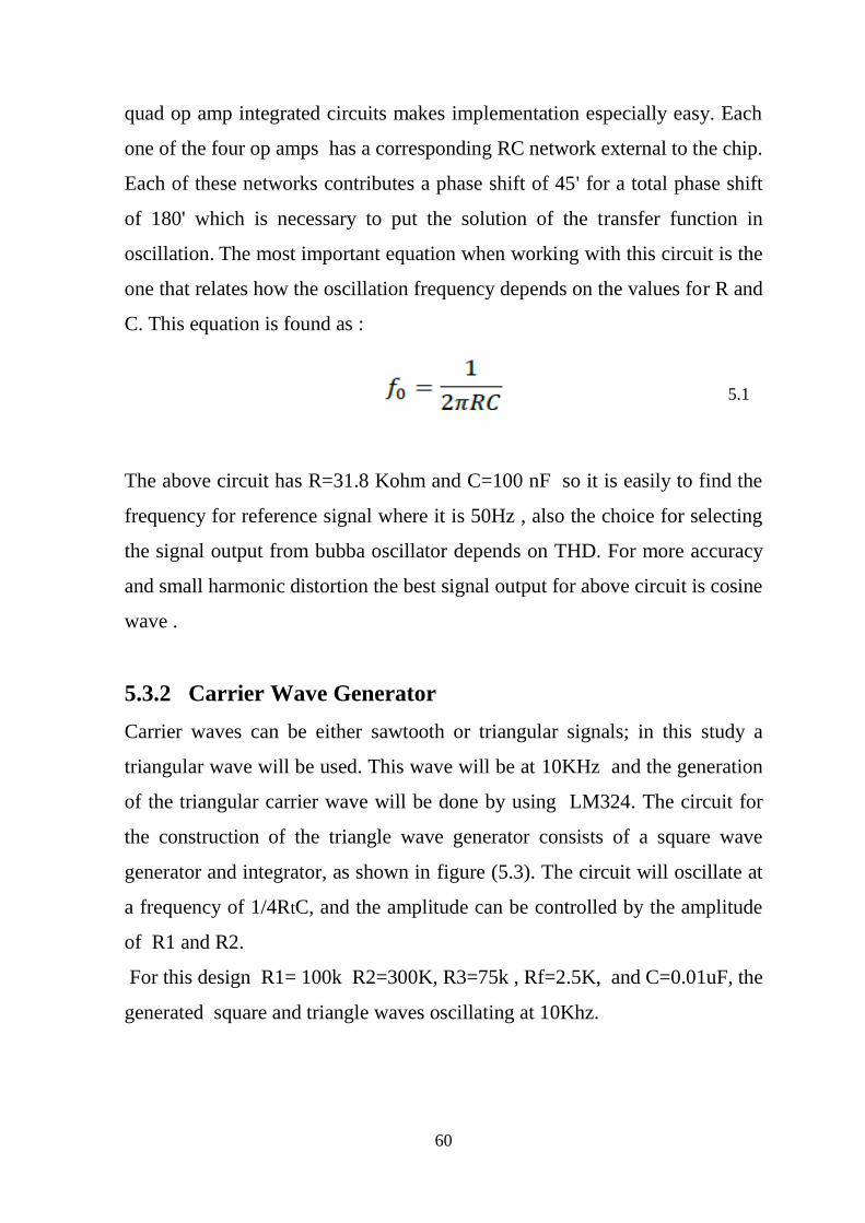
Figure 5.9: The AC output signal for the push pull converter........................68
Figure 5.10: The actual hardware for SPWM generator with FLC................68
Figure 5.11: The result output from Bubba oscillator....................................69
Figure 5.12: The result output from triangular generator...............................69
Figure 5.13: The generated pulses for SPWM generator.............................. 70
Figure 5.14: H-Bridge and driver circuit.......................................................70
Figure 5.15: SPWM full bridge inverter........................................................71
Figure 5.16: The result output signal for full load inverter...........................72
ix

xii
LIST OF TABLES
Table 4.1: Parameters of PWM inverter………………………………..40
Table 4.2: Fuzzy rules.......…………………………………………………...….50
Table 5.1: Key features of PIC16F877A……………………………….65
x

xiii
Abbreviations
A voltage-source inverter VSI
A current-source inverter CSI
Fuzzy Logic Control FLC
Center of Gravity COG
Sine Pulse Width Modulation SPWM
Total Harmonic Distortion THD
Electromagnetic Interference EMI
Pulse Width Modulation PWM
Resonant Snubber Inverter RSI
Single Input Single Output SISO
Proportional Integral PI
Printed Circuit Board PCB
Adjustable Speed Drives ASD
Uniform Pulse Width Modulation UPWM
xi

xiv
xii

CHAPTER 1
INTRODUCTION
1.1 General Introduction
DC/AC inverters are electronic devices used to produce AC power at a
desired output voltage or current and frequency. Inverters are used for many
applications, as in situations where low voltage DC sources such as batteries,
solar panels or fuel cells must be converted so that devices can run off AC
power. One example of such a situation would be converting electrical power
from a car battery to run a laptop, TV or cell phone.
Most inverters do their job by performing two methods: the first method is
converting the incoming DC into AC, then they step up the resulting AC to
main voltage level using a transformer. The second method is converting the
low voltage DC power to a high voltage DC source, then convert high DC
source to an AC waveform by using H-bridge driver.
The terms voltage-fed and current-fed are used in connection with the output
from inverter circuits. A voltage-source inverter (VSI) is one in which the DC
input voltage is essentially constant and independent of the load current
drawn. The inverter specifies the load voltage while the load dictates the
drawn current shape.
A current-source inverter (CSI) is one in which the source input is DC current
hence, the output current is constant and the load impedance determines the
output voltage.
There are many types of inverters that are different in the output sources such
as: square wave, modified sine wave and pure sine wave as shown in figure
(1.1) [1]. The square wave output has a high harmonic content, not suitable to
AC loads such as motors or transformers; therefore, square wave units are
considered as the pioneers of inverter development. A modified square wave
1

2
or modified sine wave inverter is similar to a square wave output except that
the output goes to zero volts for a time before switching positive or negative.
It is simple, low cost and is compatible with most electronic devices.
A pure sine wave inverter produces a nearly perfect sine wave output (less
than 5% total harmonic distortion) that is essentially the same as utility-
supplied grid power [2]. Thus, it is compatible with all AC electronic devices.
The mathematical model used for calculating output voltage of inverter is
( ) ∑ ( )
Where, is the frequency in Hz, t is the continuous time signal
1 is the amplitude of harmonics.
Figure 1.1: Square, Modified, and Pure Sine Wave
Most inverters have classical controllers such as proportional-integral, these
controllers are not compatible for some application because the output signal
is not pure sine wave.
1.1

3
However the total harmonic distortion influence in the loads causing high
power dissipation. Fuzzy logic controllers [3] have become the most popular
controller compared with conventional controller, since FLC can work with
imprecise inputs, handle nonlinearity and it is more robust.
Actually, power inverters that are used in Gaza strip have high THD so the
qualities of inverters are very low. Therefore, the thesis outcomes focus on
the performance of an inverter output waveform by proposing the fuzzy logic
control as a new strategy of the controller; hence, the new technique is used to
keep the output distortion at acceptable level, as the desired output of an
inverter must be pure sine wave.
1.2 Previous Studies
In 2010, Aleksey Trubitsyn [4] proposed high efficiency DC/AC power
converter for photovoltaic application, he presented the development of a
micro inverter for single-phase photovoltaic application. A multidimensional
control technique was utilize to achieve high efficiency, encompassing
frequency control, inverter and cycloconverter by phase shift control.
This work provided modified sine wave so the output have a little harmonic
distortions, which it is not compatible with all devices like motors.
In 2009, Rickard Ekström [5] presented inverter system design and control
for a wave power substation, he investigated the design of the inverter, gate
drive, filter, control system and protections for this substation. In addition,
extensive market research was done, resulting in decisions of what
components to be merchandise.
This work used SPWM without feedback controller; therefore, the output
display high drop voltage when a load is applied.

4
In 2004, Keith Jeremy McKenzie [6] proposed eliminating harmonics in a
cascaded H-Bridges multilevel inverter using resultant theory, symmetric
polynomials, and power sums. This work studied a multilevel converter with
assumed equal dc sources. The multilevel fundamental switching scheme was
used to control the needed power electronics switches. In addition, a method
presented where switching angles computed such that a desired fundamental
sinusoidal voltage produced while at the same time certain higher order
harmonics are eliminated.
This work used multilevel DC sources to generate sine wave signal so in
practical design the cost of this type inverter is very high.
In 2001, Robert A. Gannett [7] proposed control strategies for high power
four-leg voltages source inverter where it addressed some of the causes of
poor power quality and control strategies to ensure a high performance level
in inverter fed power systems.
This work used conventional controllers; therefore, the harmonic distortion
influence in some devices like fans and sound devices.
In1998, Obasohan I. Omozusi [8] proposed the operation of a single-phase
induction generator with a PWM inverter as a source of excitation. The
simulation of the single-phase induction generator, and PWM inverter was
done using device model. Matlab/Simulink was found to be a great tool in
modeling the PWM inverter and the single-phase induction generator.
This work used the inverter only to control in a single-phase induction
generator.
In1998, Yuqing Tang [9] proposed high power inverter EMI characterization
and improvement using an auxiliary resonant snubber inverter. This work
deals with electromagnetic interference where it was identified as high

5
switching (dv/dt) and (di/dt) rates interacting with inverter parasitic
components. The relation between the (dv/dt), ( di/dt ) and the EMI
generation were discussed. The EMI sources of a hard-switching single-phase
PWM inverter were identified and measured with separation of common-
mode and differential-mode noises. The noise reduction in an auxiliary
resonant snubber inverter (RSI) was presented.
1.3 Statement of the Problem:
The conventional controllers that used for power inverter are inaccurate in
some applications; therefore, the motivation was to research into new
technologies to address this problems by reducing the distortion harmonics.
The proportional-integral controller, PI which is commonly used in power
inverter as power output, is not accurate in some applications such as
transformer, fans and sound devices where the total harmonic distortion
influences the behavior of this devices also may damage this devices for long
time. Therefore, this study will focus on this problem by presenting new
technique of fuzzy logic controller to improve the performance of the
inverter, the system block diagram of the inverter is shown in figure (1.2).
Assuming Vo be the load voltage, Vref be the desired sinusoidal waveform,
and Ve = Vo − Vref be the voltage error.
Choosing the resulting error dynamic state equation can be
derived as [5]:
1.2

6
Where is the state vector, u is the control input, A is the system matrix, B
is the control matrix. The control objective is to make the output voltage
equals to a reference input.
Figure 1.2: The block diagram for power inverter with FLC
1.4 Research Objective and Methodology
1.4.1 Research Methodology
The research will be implementing as follow
1. Collecting data on the inverters types, application and schematic
circuits.
2. Designing PI controller using Matlab SISO Tool for the close loop
system.
3. Using Mamdani method to design the proposed fuzzy logic controller
with the utilization of Matlab fuzzy tools and identifying the
membership functions.

7
4. Simulating the system using Matlab and studying the behavior of the
inverter.
5. Comparing the performance of the PI controller and FL controller and
discussing the THD for the inverter system.
6. Analyzing the system and designing the schematic circuit that
contained power drivers and control system using Protuse program.
7. Building up the actual hardware inverter circuit.
1.4.2 Research Contributions
It is a well documented of the shortage of electricity in Palestine, especially in
the Gaza Strip. The people suffer from power cuts on a daily basis for a
period of not less than 8 hours, which leads to the used the small generators
including the occurrence of noise and the risk of accidents, particularly in the
small apartments, and houses. Thus, the situation leads to high demand for
other devices to replace the generators such as power inverter. The current
devices of inverter having high THD which causes problems in the loads.
This study provides the best and creative solution to this problem by
providing a new and safe product for the power inverter specifications to suit
the home devices such as lighting, television and fans and does not cause any
harm to these devices. This inverter is based on a new fuzzy logic controller
design, which regulate the output voltage and reduce the harmonic distortion
in the output signal.
1.5 Thesis Organization
The remaining chapters of this thesis are organized as follows: Chapter 2
covers the review and background for some basic principles of inverter
systems, type of inverter and harmonic distortion for the output signal.
Chapter 3 gives a review and introduction to fuzzy logic and its application,

8
fuzzy sets operations, the main concepts in fuzzy sets such as membership
functions, and linguistic variable. Chapter 4 presents the design of the system
by applying comparative study between classical and fuzzy logic controller
also the simulation results are presented to show the performance of the
proposed control system.
Chapter 5 demonstrates the hardware implementation for the proposed
system while Chapter 6 presents the conclusions, recommendation, future
works, and finial remarks.

9
CHAPTER 2
BACKGROUND & BASIC CONCEPTS
2.1 Introduction
In this chapter, the basic concept for designing power inverter is proposed to
understand the behavior of the system. The design of the inverter system is
based on voltage source inverter and the key of generating sine wave signal is
obtained by using PWM technique. This technique is used for controlling the
power inverter output by changing the modulation index for reference signal.
The pulses are obtained by comparing the reference signal with triangular
signal or sawtooth signal. The frequency of the reference signal is constant
for the inverter where it is 50HZ or 60HZ depending on the loads. The
voltage is regulated by controlling the modulation index, so the amplitude of
the reference signal is changed from 0 to 1 depending on the load.
Historically, inverters have been made with every kind of switching
apparatus, such as rotating or vibrating mechanical contacts, gas-filled
electronic valves, and thyristors (SCRs). However, in contemporary use, the
field is led by two special kinds of transistor. The first kind is the Metal-
Oxide-Semiconductor Field-Effect Transistor (MOSFET). The second type of
transistor Gate Bipolar Transistor (IGBT). For inverter system there is two
circuits topologies half bridge and full bridge. The half bridge contains two
switches and the full bridge inverter consists of four switches. This thesis,
presents the circuit that utilizes full bridge inverter with four MOSFET
transistor[1].
2.2 Type of Inverters Outputs:
Power inverters produce one of the three different types of wave output:

10
1. Square wave.
2. Modified square wave .
3. Pure sine wave.
The three different wave signals represent three different qualities of power
output. Square wave inverters result in uneven power delivery that is not
efficient for running most devices.
2.2.1 Square Wave
The earliest electronic inverters produced a square wave as shown in figure
(2.1), which can be seen as a sine wave sampled twice per cycle. A square
wave has a very high harmonic content and a Peak-to-RMS voltage ratio of
one. Because electronic loads are usually sensitive to peak voltage while
resistive loads such as incandescent lamps respond to the RMS value, the
square wave is unsuitable for general use.
Figure 2.1: Square wave signal
2.2.2 Modified square Wave
A modified sine wave inverters approximate a sine wave as shown figure
(2.2) has low enough harmonics that do not cause problem with household.
Modified sine wave inverters are designed to satisfy the efficiency
requirements of the photovoltaic system while being less expensive than pure

11
sine waveform inverters; these inverters are capable of operating a wide variety
of loads.
Figure 2.2: Modified sine wave
2.2.3 Pure Sine Wave Inverter
For any device that requires sensitive calibration, it is advisable to use a pure
sine wave inverter. This type of inverter provides output voltage waveform,
which is very similar to the voltage waveform that is received from the grid.
The sine wave as shown in figure(2.3) has very little harmonic distortion
resulting in a very clean supply and makes it ideal for running electronic
systems such as computers, digital fax and other sensitive equipment without
causing problems or noise.

12
Figure 2.3: Pure sine wave
2.3 Voltage Source Inverter and Current Source Inverter
2.3.1 Voltage Source Inverter:
The type of inverter as independently controlled AC output is considered as
the voltage waveform. The output voltage waveform is mostly remaining
unaffected by the load. Due to this property, the VSI have many industrial
applications such as adjustable speed drives (ASD) and also in power system
for FACTS (Flexible AC Transmission).
2.3.2 Current Source Inverter:
The type of inverter where the independently controlled AC output, is
considered a current waveform. The output current waveform is mostly
remaining unaffected by the load. These are widely used in medium voltage
industrial applications, where high quality waveform is required.

13
2.4 Single Phase Half Bridge & Full Bridge VSI:
2.4.1 Single Phase Half Bridge Inverter:
It consists of two semiconductor switches T1 and T2 as shown in figure
(2.4). These switches may be BJT, IGBT , MOSFET transistor etc. with a
commutation circuit. D1 and D2 are called Freewheeling diode also known as
the Feedback diodes as they feedback the load reactive power[8].
Figure 2.4: Single phase half bridge inverter
S1 is ON during the positive half cycle of the output voltage, which makes
Vo=Vdc/2 and S2 is ON during the negative half cycle which makes Vo= -
Vdc/2. Both switches must operate alternatively otherwise, there may be a
chance of short circuiting. In case of resistive load, the current waveform
follows the voltage waveform but not in case of reactive load. The feedback
diode operates for the reactive load when the voltage and current are of
opposite polarities.

14
2.4.2. Single Phase Full Bridge Inverter:
It consists of two arms with a two semiconductor switches on both arms with
antiparallel freewheeling diodes for discharging the reverse current as shown
in figure (2.5). In case of resistive-inductive load, the reverse load current
flow through these diodes. These diodes provide an alternate path to inductive
current which continue so flow during the turn OFF condition [8].
Figure 2.5: Single phase full bridge inverter
The switches are S1, S2, S3 and S4. The switches in each branch operate
alternatively so that the never in same mode (ON /OFF) simultaneously. In
practice they are both OFF for short period of time called blanking time, to
avoid short circuiting. The switches S1 and S4 or S2 and S3 should operate in
pair to get the output. These bridges are switched such that the output voltage
is shifted from one to another and hence the change in polarity occurs in
voltage waveform. If the shift angle is zero, the output voltage is also zero
and maximal when shift angle is Ɵ.

15
2.5 Pulse Width Modulation (PWM)
The most common and popular technique of digital pure-sine wave generation
is pulse-width-modulation (PWM). The PWM technique involves generation
of a digital waveform, for which the duty-cycle is modulated such that the
average voltage of the waveform corresponds to a pure sine wave. The
simplest way of producing the PWM signal is through comparison of a low-
power reference signal with carrier signal, the reference signal is the desired
output signal maybe sinusoidal or square wave, while the carrier signal is
either a sawtooth or a triangular wave at a frequency significantly greater than
the reference. The advantage of this technique is to minimize the lower order
harmonics, while the higher order harmonics can be eliminated using a filter.
There are different PWM techniques that essentially differ in the harmonic
content of their respective output voltages; thus, the choice of a particular
PWM technique depends on the permissible harmonic content in the inverter
output voltage[1],[8].
2.5.1 Single Pulse Width Modulation:
In single pulse-width modulation control, there is only one pulse per half-
cycle and the width of the pulse is varying to control the output voltage.
Figure (2.6) shows the generation of the input of single pulse width
modulation. The input signals are generated by comparing the rectangular
control signal of amplitude with triangular carrier signal . The
frequency of the control signal determines the fundamental frequency of AC
output voltage. The amplitude modulation index is defined as:
2.1

16
The RMS AC output voltage:
(
∫
( )
( )
)
√
or
√
Where the duty ratio is
Figure 2.6: Output voltage of single phase width modulation
By varying the control signal amplitude from 0 to , the pulse width
ton can be modified from 0 sec to T/2 sec and the RMS output voltage
from 0 to .
2.2
2.3

17
2.5.2 Multiple Pulse Width Modulation:
The harmonic content can be reduced by using several pulses in each half-
cycle of output voltage. The generation of gating signals for turning on and
off of transistors is shown in figure (2.7) by comparing a reference signal with
a triangular carrier wave[1].
The frequency of reference signal sets the output frequency (fo) and the
carrier frequency (fc), determines the number of pulses per half cycle (p), the
modulation index controls the output voltage. This type of modulation is also
known as uniform pulse width modulation UPWM. The number of pulses per
half cycle is found from Eq. 2.4:
where, mf = fc/fo is defined as the frequency modulation ratio.
Figure 2.7: Multiple pulse width modulation
2.4

18
The variation of modulation index m from 0 to 1 varies the pulse width, Kt,
from 0 to T/p and the output voltage from 0 to the RMS output voltage
can be found from Eq. 2.5:
√
∫
(
)
(
)
√
2.5.3 Sinusoidal Pulse Width Modulation:
Instead of maintaining the width of all pulses the same as in the case of
multiple-pulse modulation, the width of each pulse is varied in proportion to
the amplitude of a sine wave evaluated at the center of the same pulse [10].
The distortion factor and lower-order harmonics are reduced significantly.
The generation of gating signals for turning on and off of transistors is shown
in figure(2.8) by comparing a sinusoidal reference signal with a triangular
carrier wave of frequency( fc).
Figure 2.8: Sinusoidal pulse width modulation
2.5

19
The control signal is shown at the same figure this type of modulation is
commonly used in industrial applications and abbreviated as SPWM. The
frequency of reference signal (fr) determines the output frequency (fo) and
its peak amplitude (Ar) controls the modulation index m the number of
pulses per half-cycle depends on the carrier frequency. The output voltage can
be varied by varying the modulation index m the RMS output voltage can be
found from Eq. 2.6:
√∑
2.5.4 Fuzzy Sinusoidal Pulse Width Modulation:
A lot of control strategies for regulation of PWM inverters in power supplies
have been developed. Therefor a new approach for combining a fuzzy logic
controller with sinusoidal pulse-width modulator is proposed to reduce the
harmonic distortion and the output signal become pure sine wave , this type
will be explain in chapter four .
2.6 Harmonic
2.6.1 Harmonic History
Before twentieth century, the predominant use of electricity for business and
industry was power motors, lights and heating devices. These uses have little
effect on the fundamental frequency. They called linear loads, because the
current rises and falls in proportion to the voltage wave. In recent years, few
industries use devices such as rectifiers or converters, power supplies and
other device to improve product quality [11]. All of these make the current
sinusoidal waveform distorted, because the current flow was not directly
proportional to the voltage. These loads are called non-linear loads. which

20
cause waveforms that are multiples of the fundamental frequency of sine
wave to be superimposed on the base waveform, these multiples are called
harmonics, as the frequency of the second harmonic which it is two times the
fundamental frequency, the third harmonic is three times the fundamental
frequency. The combination of the sine wave with all the harmonics creates a
new non sinusoidal wave of entirely different shape is called harmonic
distortion.
2.6.2 Source of Harmonic
The main source of the harmonics is any non-linear loads that produce the
voltage harmonics and current harmonics. This occurs because the resistance
of the device is not a constant. The resistance in fact, changes during each
sine wave. So, nonlinear device is one in which the current is not proportional
to the applied voltage.
2.6.3 Effects of Harmonic Distortion in Power Systems
The effect of current distortion on power distribution systems can be serious,
primarily because of the increased current flowing in the system. In other
words, because the harmonic current doesn't deliver any power, its presence
simply uses up system capacity and reduces the number of loads that can be
powered. Harmonic current occur in a facility’s electrical system can cause
equipment malfunction, data distortion, transformer and motor insulation
failure, tripping of circuit breakers, and solid-state component breakdown
also, it is increase heat losses in transformers and wiring. Since the
transformer impedance is depend on the harmonic order for the frequency, for
example the impedance at the 5th harmonic is five times that of the
fundamental frequency. So each ampere of 5th harmonic current causes five
times as much heating as an ampere of fundamental current. More

21
specifically, the effects of the harmonics can be observed in many sections of
electrical equipment and a lot machines and motors.
2.6.4 Harmonic Distortion of Inverter:
The switch in the simple inverter described above, when not coupled to an
output transformer, produces a square voltage waveform due to its simple off
and on nature as opposed to the sinusoidal waveform that is the usual
waveform of an AC power supply. Using Fourier analysis, periodic
waveforms are represented as the sum of an infinite series of sine waves. The
sine wave that has the same frequency as the original waveform is called the
fundamental component. The other sine waves, called harmonics, that are
included in the series have frequencies that are integral multiples of the
fundamental frequency. Fourier analysis can be used to calculate the total
harmonic distortion (THD), which it is the square root of the sum of the
squares of the harmonic voltages divided by the fundamental voltage.
2.6.5 Harmonic in Square Wave:
square wave is a non-sinusoidal periodic waveform which can be represented
as an infinite summation of sinusoidal waves as shown in figure (2.9), in
which the amplitude alternates at a steady frequency between fixed minimum
and maximum values, with the same duration at minimum and maximum the
transition between minimum to maximum is instantaneous for an ideal square
wave.
2.7

22
Figure 2.9: Harmonic waves for square wave
Examining the harmonic for square wave
Using Fourier expansion with cycle frequency f over time t, we can represent
an ideal square wave with a peak to peak amplitude of 2 as an infinite series
of the form:
The FFT for square wave is shown in figure (2.10) implies that the lowest
frequency is called the fundamental frequency and multiples of it are called
2.8
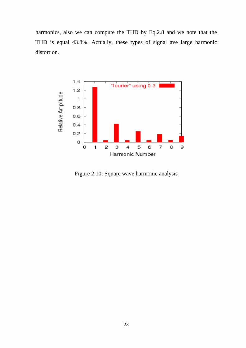
23
harmonics, also we can compute the THD by Eq.2.8 and we note that the
THD is equal 43.8%. Actually, these types of signal ave large harmonic
distortion.
Figure 2.10: Square wave harmonic analysis

24
CHAPTER 3
FUZZY LOGIC CONTROL
3.1 History Of Fuzzy Logic
In early 1960s, Lotfi A. Zadeh, a professor at University of California at
Berkley well respected for his contributions to the development of system
theories, began to feel that traditional systems analysis techniques were too
precise for many complex real-world problems. The idea of grade of
membership, which is the concept that became the backbone of fuzzy set
theory, occurred to him in 1964 [12] , which lead to the publication of his
seminal paper on fuzzy sets in 1965 and the birth of fuzzy logic technology
[13]. In 1974, S. Assilian and E. H. Mamdani in United Kingdom developed
the first fuzzy logic controller, which was for controlling a steam generator
[14]. In the 1980’s, several important industrial applications of fuzzy logic
was launched successfully in Japan. After eight years of persistent research,
development, and deployment efforts, Yasunobu and his colleagues at Hitachi
put a fuzzy logic-based automatic train operation control system into
operation in Sendai city’s subway system in 1987 [15]. Another early
successful industrial application of fuzzy logic is a water-treatment system
developed by Fuji Electric. These and other applications motivated many
Japanese engineers to investigate a wide range of novel fuzzy logic
applications. This lead to the fuzzy boom. The fuzzy boom in Japan was a
result of close collaboration and technology transfer between universities and
industries.
25
3.2 Introduction
Fuzzy logic is a branch of artificial intelligence that deals with reasoning
algorithms used to emulate human thinking and decision making in machines.
These algorithms are used in applications where process data cannot be
represented in binary form. For example, the statements “the air feels cool”
and “he is young” are not discrete statements. They do not provide concrete
data about the air temperature or the person’s age (i.e., the air is at 65°F or the
boy is 12 years old). It is a superset of conventional (Boolean) logic that has
been extended to handle the concept of partial truth. In the ( Boolean ) logic
we see that the results for any operation can be true or false if we refer to true
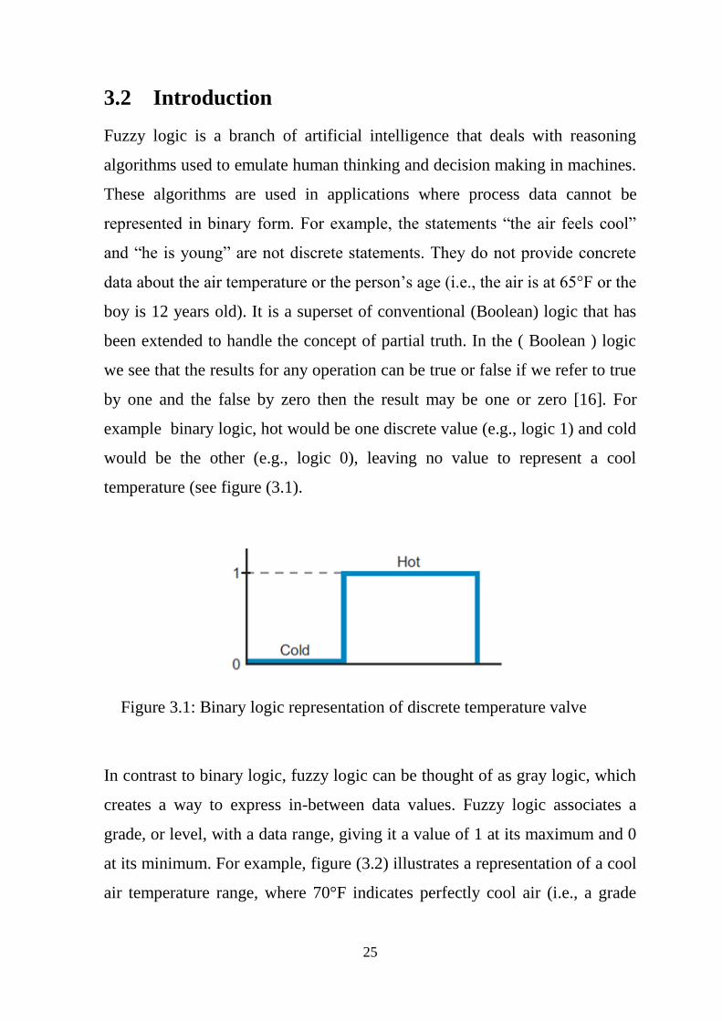
by one and the false by zero then the result may be one or zero [16]. For
example binary logic, hot would be one discrete value (e.g., logic 1) and cold
would be the other (e.g., logic 0), leaving no value to represent a cool
temperature (see figure (3.1).
Figure 3.1: Binary logic representation of discrete temperature valve
In contrast to binary logic, fuzzy logic can be thought of as gray logic, which
creates a way to express in-between data values. Fuzzy logic associates a
grade, or level, with a data range, giving it a value of 1 at its maximum and 0
at its minimum. For example, figure (3.2) illustrates a representation of a cool
air temperature range, where 70°F indicates perfectly cool air (i.e., a grade

26
value of 1). Any temperature over 80°F is considered hot, and any
temperature below 60°F is considered cold.
Figure 3.2: Cool air temperature range
3.3 Classical Sets versus Fuzzy Sets
The concept of a classical set is very fundamental to pure and applied
mathematics. Intuitively, a set is defined as any collection of definite and
distinct objects that is conceived as a whole, also objects that are included in a
set are usually called its members.
Classical sets satisfy two basic requirements: first, members of each set
are distinguishable from one another, and second, for any given object it
is specified whether the object is, or is not, a member of the set the function
of crisp set is
3.1

27
Fuzzy sets differ from classical sets by rejecting the second requirement.
Contrary to classical sets, fuzzy sets do not require sharp boundaries that
separate their members from other objects.
The membership of any object in a given fuzzy set is not a matter of
affirmation or denial, as is required for classical sets, but a matter of degree
which the membership between 0 and 1 .
3.4 Fuzzy Set Operations
Basic operations on sets in crisp set theory are the set complement, set
intersection, and set union. Fuzzy set operations are very important because
they can describe intersections between variables for a given element "x" of
the universe, the following function theoretic operations for the set theoretic
operations of complement, intersection, and union are defined[3][17]:
1) Complement (NOT Operation):
Consider a fuzzy set "A" in universe "X". its complement "A" as shown in
figure (3.3) which A’ XA’(x) = 1 – XA(x).
Figure 3.3: Complement of fuzzy sets A

28
2) Intersection (AND Operation):
Consider two fuzzy sets "A" and "B" in universe "X". as in figure (3.4) where
A B XA B(x) = min(XA(x),XB(x)).
Figure 3.4: Intersection of fuzzy sets A and B
3) Union (OR Operation):
Consider two fuzzy sets "A" and "B" in universe "X". is the whole
area covered by the sets as shown in figure (3.5) where A B(x) =
max(A(x), B(x)) .
Figure 3.5: Union of fuzzy sets A and B

29
3.5 Fuzzy logic Control Component
In this part of this chapter, the main components of a fuzzy logic controller
are discussed and a simple example is implemented. The three main actions
performed by a fuzzy logic controller are:
• fuzzification
• fuzzy processing
• defuzzification
As shown in figure (3.6), when the fuzzy controller receives the input data, it
translates it into a fuzzy form this process is called fuzzification.
Figure 3.6: Fuzzy logic controller operation
The controller performs fuzzy processing, which involves the evaluation of
the input information according to IF…THEN rules created by the user
during the fuzzy control system’s programming and design stages. Once the
fuzzy controller finishes the rule-processing stage and arrives at an outcome
conclusion, it begins the defuzzification process. In this final step, the fuzzy
controller converts the output conclusions into “real” output data (e.g., analog
counts) and sends this data to the process via an output module interface.

30
3.5.1 Fuzzification Component:
The fuzzification process is the interpretation of input data by the fuzzy
controller. Fuzzification consists of two main components:
(a) Membership functions
(b) Labels
a . Membership Functions.
During fuzzification, a fuzzy logic controller receives input data, also known
as the fuzzy variable, and analyzes it according to user-defined charts called
membership functions (see figure 3.7). Membership functions group input
data into sets, such as temperatures that are too cold, motor speeds that are
acceptable, etc. The controller assigns the input data a grade from 0 to 1 based
on how well it fits into each membership function (e.g., 0.45 too cold, 0.7
acceptable speed).
Figure 3.7: Membership function chart
Membership functions can have many shapes, depending on the data set, but
the most common are the S, , Z, shapes shown in figure (3.8).
Note that these membership functions are made up of connecting line
segments with a maximum of four end points.
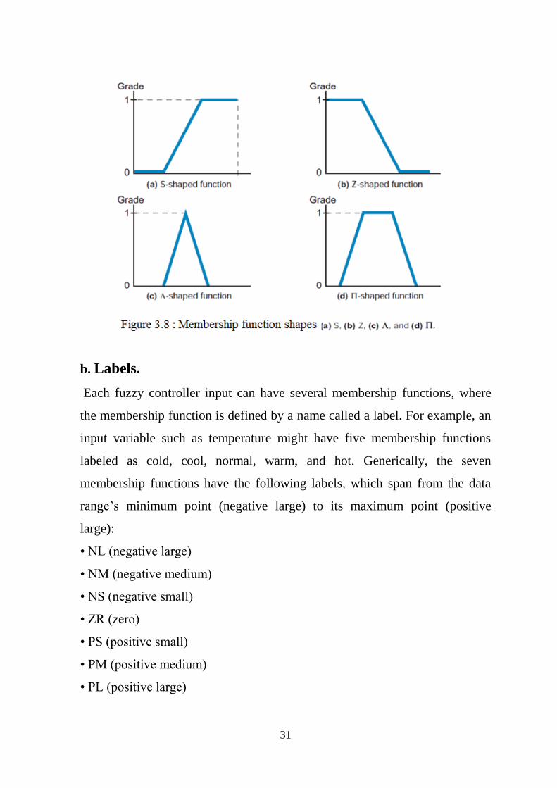
31
b. Labels.
Each fuzzy controller input can have several membership functions, where
the membership function is defined by a name called a label. For example, an
input variable such as temperature might have five membership functions
labeled as cold, cool, normal, warm, and hot. Generically, the seven
membership functions have the following labels, which span from the data
range’s minimum point (negative large) to its maximum point (positive
large):
• NL (negative large)
• NM (negative medium)
• NS (negative small)
• ZR (zero)
• PS (positive small)
• PM (positive medium)
• PL (positive large)

32
figure (3.9) illustrates an example of an input variable with seven shaped
membership functions using all of the possible labels. A group of membership
functions forms a fuzzy set.
Figure 3.9: Fuzzy logic input seven membership function labels
3.5.2 Fuzzy Processing Components (Mamdani method)
A fuzzy controller or model uses fuzzy rules, which are linguistic if-then
statements involving fuzzy sets, fuzzy logic, and fuzzy inference. Fuzzy rules
play a key role in representing expert control/modeling knowledge and
experience and in linking the input variables of fuzzy controllers/models to
output variable (or variables). The major types of fuzzy rules exist, namely,
Mamdani fuzzy rules ,which is the most commonly used fuzzy inference
technique. The Mamdani-style fuzzy inference process is performed in three
steps [18]:
1) Fuzzification of the crisp input variables
2) Rule evaluation.
3) Fuzzy outcome calculation

33
To illustrate the fuzzy inference let's examine a simple two-input one-output
problem that includes three rules:
Rule (1) …. IF X is A3 OR Y is B1 THEN z is C1
Rule (2)…. IF X is A2 AND Y is B2 THEN z is C2
Rule (3)…. IF X is A1 THEN z is C3
Step 1: Fuzzification
The first step in the application of fuzzy reasoning is a fuzzification of inputs
in the controller, which is to take the crisp inputs, x1 and y1, and determine
the degree to which these inputs belong to each of the appropriate fuzzy sets.
It means that to every crisp value of input we attribute a set of degrees of
membership (mj, j=1,n) to fuzzy sets defined in the universe of discourse for
that input as shown in figure (3.10)[17].
Figure 3.10: Fuzzification stage
Step 2: Rule evaluation
The second step is to take the fuzzified inputs, (x=A1) = 0.5, (x=A2) = 0.2,
(y=B1) = 0.1 and (y=B2) = 0.7, and apply them to the antecedents of the
fuzzy rules. If a given fuzzy rule has multiple antecedents, the fuzzy operator

34
(AND or OR) is used to obtain a single number that represents the result of
the antecedent evaluation. This number (the truth value) applied to the
consequent membership function. To evaluate the disjunction of the rule
antecedents, the OR fuzzy operation is used. The most popular approaches
used for the union to get the maximum value is AB(x) = max [A(x),
B(x)].
Similarly, in order to evaluate the conjunction of the rule antecedents, we
apply the AND fuzzy operation intersection which used minimum approach:
AB(x) = min [A(x), B(x)] .The rule evaluations are clearly appears in
figure (3.11)[17] .
Figure 3.11: Rule evaluation in Mamdani method

35
Step 3: Fuzzy outcome calculation
We take the membership functions of all rule consequents previously (Max-
Min Composition) or (Max-Product Composition) and combine them into a
single fuzzy set as figure (3.12).
Figure 3.12 Fuzzy outcome evaluations
3.5.3 Defuzzification
The final output value from the fuzzy controller depends on the
defuzzification method used to compute the outcome values corresponding to
each label. The defuzzification process examines all of the rule outcomes
after they have been logically added and then computes a value that will be
the final output of the fuzzy controller. Thus, during defuzzification, the
controller converts the fuzzy output into a real-life data value. There are many
defuzzification methods, but all are based on mathematical algorithms. Some
commonly used defuzzifying methods which are Center of gravity (COG),
weighted average method, mean of maximum (MOM) and smallest of
maximum (SOM) [17]. In this thesis the COG method and MOM will be
used as describe below :

36
4.675.05.05.05.02.02.02.02.01.01.01.0
5.0)100908070(2.0)60504030(1.0)20100(
COG
The mean of maximum method (MOM)
The mean of maxima method generates a crisp control action by averaging
the support values which their membership values reach the maximum. In the
case of discrete universe:
Where l is the number of the quantized i values which reach their maximum
memberships.
Center of gravity (COG)
The center of gravity method, also referred to as “calculating the centroid,”
mathematically obtains the center of mass of the triggered output membership
functions. Figure (3.13) illustrates the centroid calculation for the example
previously illustrated in figure (3.10). In mathematical terms, a centroid is the
point in a geometrical figure whose coordinates equal the average of all the
other points comprising the figure this point is the center of gravity of the
figure.Mathematically the centre of gravity (COG) can be expressed as:
∫ ( )
∫ ( )
3.2
3.3

37
Figure 3.13: COG approach in defuzzification stage
3.6 Advantages and Disadvantages of Mamdani Method
3.6. 1 Advantages of The Mamdani Fuzzy Method:
It is intuitive and simple to build.
It is widely used for second order systems with both linear and
nonlinear characteristics.
It has widespread acceptance.
It is well suited to human feeling.
3.6. 2 Disadvantages of The Mamdani Fuzzy Method:
It is only suited to the long delay system, such as the temperature
control system, since it is too simple to control the process quickly.
It needs additional device to improve the efficiency, when it controls
the high frequent input system.

38
CHAPTER 4
CONTROLLER DESIGN & SIMULATION RESULT
4.1 Introduction
Power electronic inverters are widely used in various industrial drive
applications such as uninterruptible power supplies (UPS), medical
equipment and communication systems so there is increasing demand for high
quality power inverter. Pulse-width modulated PWM inverter has been used
as a key element for a high performance power conversion system. The
output voltage is required to be sinusoidal with minimum total harmonic
distortion (THD). This is usually achieved by employing a combination of
pulse width modulation (PWM) scheme and a second order filter at the output
of the inverter [1][8]. In industries, the THD value should not exceed 5%
according to IEEE standard. Many control techniques have been proposed for
obtaining pure sinusoidal output with good voltage regulation and fast
dynamic response. Conventional closed loop control scheme employs PI
controller is commonly used to achieve the desired output. Sometimes, there
is problem using this kind of controller because it needs the mathematical
model and tuning the parameter is very difficult in some application. To
overcome this problem new controller based on fuzzy logic control is used to
solve this problem. Dominance of FLC’s over the conventional controllers
has become tight as it can work with imprecise inputs, can handle
nonlinearity and it is more robust than conventional nonlinear controllers.
In this chapter, the comparative study has been carried out between FLC
controller and PI controller where both controllers are designed for harmonic
elimination in sinusoidal PWM inverters.

39
4.2 System Description for Single Phase DC-AC PWM
Inverter
As shown in figure (4.1), the inverter consists of two sides (A, B) which
supplies a single-phase AC output voltage Vout to the load. A certain
switching algorithm is applied to each of the four switch modules T1, T2, T3,
and T4 in order to control the inverter to generate the desired sinusoidal
output with the desired frequency and magnitude[19].
Figure 4.1 :Single phase full bridge inverter
In this study the unipolar SPWM technique is used to drive the inverter
because it gives low THD and decreases the power switches losses.
Comparing a control signal Vcontrol1 with the carrier signal results a logic
signal to control the switches in side A, and comparing of Vcontrol2 with the
carrier signal results in logic signal to control the switches in side B as shown
in figure (4.2)[11].

40
Figure 4.2: Unipolar PWM scheme
4.3 Component Selection
The magnitude of the ripple current and ripple voltage in the output of the
inverter is determined by the size of the LC filters. The filter size has been
chosen, and the design specification for the proposed inverter circuit is shown
in Table 4.1.
Table 4.1 : Parameters of PWM inverter

41
4.4 Filter Design
A proper design of the LC filter results in a great reduction of the inverter
output harmonics; hence, provides a very clean power to the load. The
inductor ripple current depends on the size of the inductor and switching
frequency. Figure (4.3) shows the ripple waveform of the inductor current
value of the inductance of the output filter inductor is given by Eq.4.1[20].
Figure4.3: Inductor ripple current
where is the DC bus voltage, Δi is the inductor ripple current and (fs) is
the inverter switching frequency. The output filter capacitor size is
determined by the allowable output voltage ripple Δ and can be calculated
from Eq.4.2 [20].
4.2
4.1

42
If the DC input voltage is limited to 350 volt and the switching frequency is
limited to 10 KHz, and if the maximum inductor ripple current is limited to
20% of the maximum peak to peak output current, then, obtained such
= 1.768 mH. The maximum ripple voltage is limited to 1% of the
maximum peak to peak output voltage, then, is obtained such = 0.229
uF.
4.5 The Mathematical Model for Single Phase Inverter
The mathematical model for the voltage controlled single-phase full bridge
inverter based on bipolar voltage switching with Sinusoidal Pulse Width
Modulation (SPWM) is considered here. It is assumed that all components are
ideal. Figure (4.4) shows a schematic representation of the voltage controlled
full-bridge inverter[19].
Figure 4.4: Schematic diagram for inverter with LC filter
From figure (4.4) the following deferential equations have been derived
which represents the linear model of L-C filter and load of the inverter.

43
( ) ( ) ( ) ( )
( ) ( ) ( ) ( )
( ) ( )
( ) ( ) ( )
Figure (4.5) shows the linear model of the inverter system (PWM inverter
plus the output filter and load), in which the proportional gain K represents
the PWM inverter is equal to / ( is the voltage of DC power
supply and is the peak voltage of triangular carrier wave).
Figure 4.5: Block diagram of the linear model for PWM inverter
Based on the analysis of figure (4.5), the system transfer function can be
obtained as shown in Eq. (4.8).
4.3
4.4
4.5
4.6
4.7

44
since is very small so we can neglect it and the transfer function in
Eq.(4.8) can be rewritten as :
4.6 Designing Controller
In figure (4.6), single phase load is connected to the SPWM voltage source
inverter, the load voltage, , is compared with the reference signal and the
error signals are passed through controller to generate the pulses which are
operated to produce sinusoidal signal output with small harmonic
distortion[19] [21].
Figure 4.6: Block diagram for the system with controller
4.8
4.9

45
4.6.1 Designing PI Controller In control engineering, PI Controller (proportional-integral controller) is a
feedback controller which drives the plant to be controlled by a weighted sum
of the error (difference between the output and desired set-point) and the
integral of that value[22]. It is a special case of the PID controller in which
the derivative (D) part of the error is not used. The PI controller is
mathematically denoted as:
where u is the control signal and e is the control error (e = r - y), the reference
value is also called the set point. The controller parameters are proportional
gain k, integral gain parameterized as:
Where k is gain of the controller and is the integral time constant. Integral
control action added to the proportional controller converts the original
system into high order. Hence, the control system may become unstable for a
large value of K. Since roots of the characteristic equation may have positive
real part, so the proportional control action tends to stabilize the system, while
the integral control action tends to eliminate or reduce steady-state error in
response to various inputs. As the value of is increased:
Overshoot tends to be smaller
Speed of the response tends to be slower
4.10
4.11

46
4.6.2 Selection of PI Controller Parameter
The parameters of the proportional and integral controller in the voltage loop
is selected by using the MATLAB/ SISO tools for the approximate
linearized control model of the inverter by ignoring the resistance as
shown in figure (4.7).
Figure 4.7: An approximate linearized control model
The feedback signal of the load voltage obviously have to be scaled down to
low voltage control signals which the feedback signals are converted to per
unit (pu) values of full load for example (1/unit) voltage represent 311 V
(√2*220) and the triangular carrier waveform also has amplitude of 1 pu.
4.6.3 Closed Loop Control Design
By applying the MATLAB SISO tool as figure (4.8) the PI controller for the
close loop system is implemented and the parameter =1.6344 and =
28181 which grantee all the poles lie in the left half plane. The stability of
the closed-loop system must be ensured by root locus plot, and step response
where the most important aspect in this design is the steady state error, peak
overshot and settling time.

47
Figure 4.8: Closed loop design by MATLAB SISO TOOLS
From the root locus plot as shown in figure (4.9) it is noted that the over all
closed loop system is stable due to the location of the root locus which are
located on the left of the imaginary axis. The step response is shown in figure
(4.10), where the settling time is approximately equal to the required value
which is 0.182 ms. The peak over shoot is 3.62% and the steady state error of
the output voltage is equal to zero.
Figure 4.9: Root locus design for closed loop system

48
Figure 4.10: Step response for the system
4.7 Design of Fuzzy Logic Controller
FL is a direct method for controlling a system without the need of a
mathematical model. FL gets crisp data from various sensors these data are
changed to linguistic or fuzzy membership functions via the fuzzification
process after that, they go through a set of fuzzy “IF-THEN” rules in an
inference engine and result in fuzzy outputs these fuzzy outputs changed back
to crisp values by the defuzzification.
The fuzzy controller for the inverter system is implemented in MATLAB
using the fuzzy logic toolbox. This toolbox allows for the creation of input
membership functions, fuzzy control rules, and output membership functions
[23]. To implement the fuzzy controller for the system as shown in figure
(4.11), it should have two input and one output and the membership function
is chosen to be triangular shape as it is demonstrated in figure (4.12).

49
Figure 4.11: Schematic diagram for the system with fuzzy controller
Figure 4.12: Fuzzy membership for input and output

50
which have PB(positive big), PM(positive mediam), PS(positeve small)
,Z(zero), NS(negative small), NM(negative mediam) and NB(negative big)
the input is taken as error (e) and the change in error (Δe) .
A 7*7-membership function having 49 rules are taken into account, where it
is describe in Table 4.2.
Table 4.2: Fuzzy rules
The rule base contains linguistic variables is provided based on experience
and it should have smooth surface as show in figure (4.13).
Figure 4.13: Input output relationship surface

51
4.8 Simulation Result
In this section, Matlab simulation for the proposed system is implemented
with controllers and the comparative study between classical PI controller and
fuzzy logic controller is discussed with emphasis on the influence of the
harmonic distortion in the output voltage and current for the load.
4.8.1 PI Controller Simulink
The block diagram is shown in figure (4.14) and it contains the universal H-
bridge, LC filter, pulse width generator and the PI controller with the
parameter of KP=1.6344 and Ki=28181 as designed in previous section. The
feedback gain is 1/310. The aim of this design is tracking sinusoidal signal
with small harmonic distortion. The carrier frequency was selected as a
triangular wave with 10kHz base frequency and the simulation was activated
for the system by applying the FFT analysis from the GUI tools.
Figure 4.14: Matlab Simulink for PWM inverter under PI controller

52
The output voltage for the load as figure (4.15) is sinusoidal wave with peak
output voltage equal 310.4 volt (RMS value equal 219.48 volt and the
frequency at 50 Hz), and the THD is about 8.04%. This distortion is grater
than IEEE which recommends 5%. Figure (4.16) describe the output current
for the load which has peak value equal 7.05A (RMS equal 4.98A) and THD
is the same as voltage output distortion.
Figure 4.15: Load voltage and spectrum analyzer for full load PWM inverter
under PI controller

53
Figure 4.16: Load current and spectrum analyzer for full load PWM inverter
4.8.2 Fuzzy Controller Simulink
By applying the fuzzy tools in Matlab, the model of the system is
implemented with fuzzy logic controller as figure (4.17). This controller is
based on Mamdani method as uses 49 rules as shown in Table 2.
The membership for the input and output is described as figure (4.12) and the
fuzzy output is defuzzyficated by the centroid method to convert the signal
to crisp signal .

54
Figure 4.17: Input and output membership by Matlab fuzzy logic control tool
Before simulating the system, it should be sent the file of the fuzzy controller
to workspace to start simulation. The block diagram in simulink is described
by figure (4.18) and the output voltage result for the load is shown in figure
(4.19).
Figure 4.18: Matlab simulation for PWM inverter under fuzzy controller

55
The output is a sinusoidal wave with peak output voltage equal 309.5 volt
where the RMS value equal 219 volt and the output frequency 50 Hz also it
can be seen that the THD is equal 3.69%, which is well below the IEEE
recommendation. So, it can be observed that the fuzzy logic controller has
resulted in better than PI controller also the output current result for the load
as figure(4.20) has peak value equal 7.03A ( RMS equal 4.97A) and THD is
the same as voltage output distortion .
Figure 4.19: Load voltage and spectrum analyzer for full load PWM inverter
under fuzzy logic controller

56
Figure 4.20: Load current and spectrum analyzer for full load PWM inverter
under fuzzy logic controller

57
CHAPTER 5
HARDWARE IMPLEMENTATION FOR PROPOSED SYSTEM
5.1 Introduction
In this chapter, the hardware implemented for the SPWM single phase
inverter design is based on four schematic circuit which are: The push pull
converter, PWM generator, MOSFET H-bridge and the fuzzy controller. The
push pull converter is used to convert the low voltage coming from battery to
high voltage where the standard voltage for the liquid battery is 12.6 v. The
PWM generator is the main object in this design and it is done by comparing
the reference signal with carrier signal. This signal is generated by using
operational amplifier such as IC LM324 to generate the pulses that fed the
gate. Actually the gate needs specific voltage to drive the MOSFET transistor
in safe mode which guarantee that the transistor is fully turn on. The IR2110
integrated circuit is used to drive this transistor. Then a microcontroller with
fuzzy rules is used to control PWM generator. The following design was
implemented by the Proteus design suite simulator program and the Micro C
language used to program the microcontroller[1].
5.2 Push Pull Converter
Push-pull converter uses the transformer in a more traditional manner to
transfer the energy directly between input and output. The schematic circuit
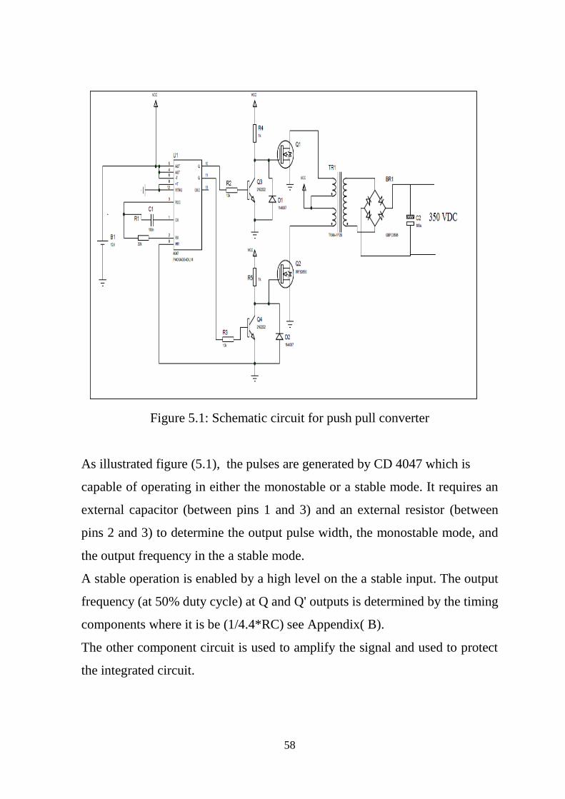
for push pull converter proposed as figure (5.1) where the input for the
converter is 12 VDC coming from battery. The output will be 350 VDC this
mean that the transformer to be used is step up type . The output signal for
transformer will be AC squared wave. The bridge rectifier BR1 rectifies this
wave again and the capacitor is used to filter the output DC signal by
removing the ripples.
58
Figure 5.1: Schematic circuit for push pull converter
As illustrated figure (5.1), the pulses are generated by CD 4047 which is
capable of operating in either the monostable or a stable mode. It requires an
external capacitor (between pins 1 and 3) and an external resistor (between
pins 2 and 3) to determine the output pulse width, the monostable mode, and
the output frequency in the a stable mode.
A stable operation is enabled by a high level on the a stable input. The output
frequency (at 50% duty cycle) at Q and Q' outputs is determined by the timing
components where it is be (1/4.4*RC) see Appendix( B).
The other component circuit is used to amplify the signal and used to protect
the integrated circuit.

59
5.3 SPWM Generators
PWM generator will be implemented by comparing reference signal with
carrier signal, the reference signal will be sine wave signal with 1 volt /50HZ
and the carrier signal is triangular wave with amplitude 1 volt /10KHZ the
result for comparing tow signal is SPWM pulses.
The implemented circuit for SPWM pulses is based on three schematic
circuits where it is bubba oscillator, carrier wave generator and the
comparator circuit.
5.3.1 Bubba Oscillator
The ability to generate a periodic signal without any crystals or resonators and
using only a DC input source is useful for a large number of applications.
This is exactly what the Bubba oscillator is capable of. Using only a single
power supply in the unipolar version, the Bubba oscillator can create low
distortion sine waves using op amps [24].
The implemented schematic circuit is shown in figure (5.2). It uses four
stages to yield a remarkably stable output frequency. The availability of
Figure 5.2: Schematic circuit for bubba oscillator
60
quad op amp integrated circuits makes implementation especially easy. Each
one of the four op amps has a corresponding RC network external to the chip.
Each of these networks contributes a phase shift of 45' for a total phase shift
of 180' which is necessary to put the solution of the transfer function in
oscillation. The most important equation when working with this circuit is the
one that relates how the oscillation frequency depends on the values for R and
C. This equation is found as :
The above circuit has R=31.8 Kohm and C=100 nF so it is easily to find the
frequency for reference signal where it is 50Hz , also the choice for selecting
the signal output from bubba oscillator depends on THD. For more accuracy
and small harmonic distortion the best signal output for above circuit is cosine
wave .
5.3.2 Carrier Wave Generator
Carrier waves can be either sawtooth or triangular signals; in this study a
triangular wave will be used. This wave will be at 10KHz and the generation
of the triangular carrier wave will be done by using LM324. The circuit for
the construction of the triangle wave generator consists of a square wave
generator and integrator, as shown in figure (5.3). The circuit will oscillate at
a frequency of 1/4RtC, and the amplitude can be controlled by the amplitude
of R1 and R2.
For this design R1= 100k R2=300K, R3=75k , Rf=2.5K, and C=0.01uF, the
generated square and triangle waves oscillating at 10Khz.
5.1

61
Figure 5.3: Schematic circuit for triangular generator
5.3.3 The Comparator Circuit
The final step for getting PWM pulses is to make comparison for the signals
above this comparing is based on three procedure:
Step 1
Shift the carrier wave by one to be in positive y- axes side. This step is done
by using adder circuit .
Step 2
Select the half cycle for reference signal and compare it with shifted carrier
wave to get Vgate1.
Step 3
Use the same procedure above to get Vgate2 but it should use the inverse of
reference signal.
Figure (5.4) show the schematic circuit for all procedures by using Protuse
simulator, the PWM generator is tested for 1KHz carrier frequency and the
result signals is obtained by digital oscilloscope simulation as figure (5.5).

62
Figure 5.4: Schematic circuits for comparator circuit
Figure 5.5: The output waves for PWM generator

63
5.4 H-Bridge and Driver Circuit
Generating a sine wave centered on zero volts requires both a positive and
negative voltage across the load, for the positive and negative parts of the
wave, respectively. This can be achieved from a single source through the use
of four MOSFET IRF740 switches arranged in an H-Bridge configuration.
Level translation between PWM signals and voltages is required to forward
bias high side N-Channel MOSFETS, the IR2110 MOSFET driver integrated
circuit was chosen where the high and low side drive device exceeds all
requirements for driving the MOSFETs in the bridge. It is capable of handling
up to 500V at a current rating of 2A at fast switching speeds. This device is
required to drive the high side MOSFETS in the circuit designated HO, due to
the fact that the gate to source voltage must be higher than the drain to source
voltage, which is the highest voltage in the system. A typical connection of a
single IR2110 device is shown in figure (5.6).
Figure 5.6: Typical connections for IR2110 driver

64
Operation of the IR2110 device will be controlled through generated PWM
signals. The PWM signal will be fed to the HIN and LIN pins simultaneously.
If the internal logic detects a logic high, the HO pin will be driven; if a logic
low is detected, the LO pin will be driven. The SD pin controls shut down of
the device and will be unused and tied to ground. A diagram of the H-Bridge
circuit with MOSFETS and drivers is shown in figure (5.7).
Figure 5.7: Schematic circuit for full bridge inverter with driver
5.5 Design Fuzzy Controller
In many application the controller is the main part of the system and changing
it depend on the task of application. In this project, the PIC 16F877A
microcontroller is used to implement the fuzzy controller. The PIC16F877A

65
provides several advantages over other microcontrollers. Different series of
PIC microcontroller are popular because of high performance, low cost, low
power consumption and small in size. The PIC 16F877A uses 35 single word
instructions, and has 20MHZ operating frequency. The key features of PIC
16F877A are shown in table 5.1.
Table 5.1: Key features of PIC16F877A
5.5.1 How to Build Program in Microcontroller
Microcontrollers were originally programmed only in assembly language, but
various high-level programming languages are now also in common use to
target microcontrollers. These languages are either designed specially for the
purpose, or versions of general purpose languages such as the C programming
language. The most common program for this application is MikroC, a
powerful, feature rich development tool for PICmicros. It is designed to
provide the possible solution for developing applications for embedded
systems, without compromising performance or control.

66
5.5.2 The Operation of Fuzzy Controller
Output voltage for the system is sensed and scaled to per unit for the based
voltage 220 volt RMS, then it evaluates the error between the actual and set
value. This result determines the main fuzzy rules of the system. the
following criteria for fuzzy controller operation are as follow :
i. If the output of the inverter deviates far from the reference, the change
of modulation index must be large to bring the output to the reference
quickly.
ii. If the output of the inverter is approaching the reference, small change
of modulation index is necessary.
iii. If the output of the inverter is near the reference and is approaching it
rapidly the modulation index must be kept constant so as to prevent
further deviation.
iv. If the reference is reached and the output is still changing the
modulation index must be changed a little bit to prevent the output
from moving away.
v. If the reference is reached and the output is steady the modulation
index remain unchanged.
vi. If the output is larger than the reference, the sign of the change of
modulation index must be negative and vice versa.
Fuzzy logic processing runs under these rules and the rules related to the rate
of change of the set/actual offset, which allows a very smooth adjustment of
voltage rate. Input data of the offset is calculated by means of taking relative
voltage difference of actual voltage to the set value as shown below:-
Error (E) = (Actual voltage of the System) - (Set Value)
Input data for integral error (IE) is the summation between the current value
of error (En) and the previous value of (En-1):-
Rate of integral error (IE) = ((En) + (En-1))

67
The analog inputs is stored in 10-bit A/D converter in microcontroller and the
output of modulation index takes values from 0 to 255 this value is converted
to analog by using external D/A to keep the modulation index from 0 to 1.
5.6 Actual Hardware Implementation
The following implementation hardware circuits are designed based on the
results of the circuit that was designed by the simulation for example; figure
(5.8) shows the actual hardware implementation for the push pull converter
where the input is 12.6 VDC from battery and the output is 350V.
The output signal for the implemented circuit tested by oscilloscope before
rectifying where it should to be square wave signal as shown in figure (5.9).
Figure 5.8: The actual hardware for push pull converter
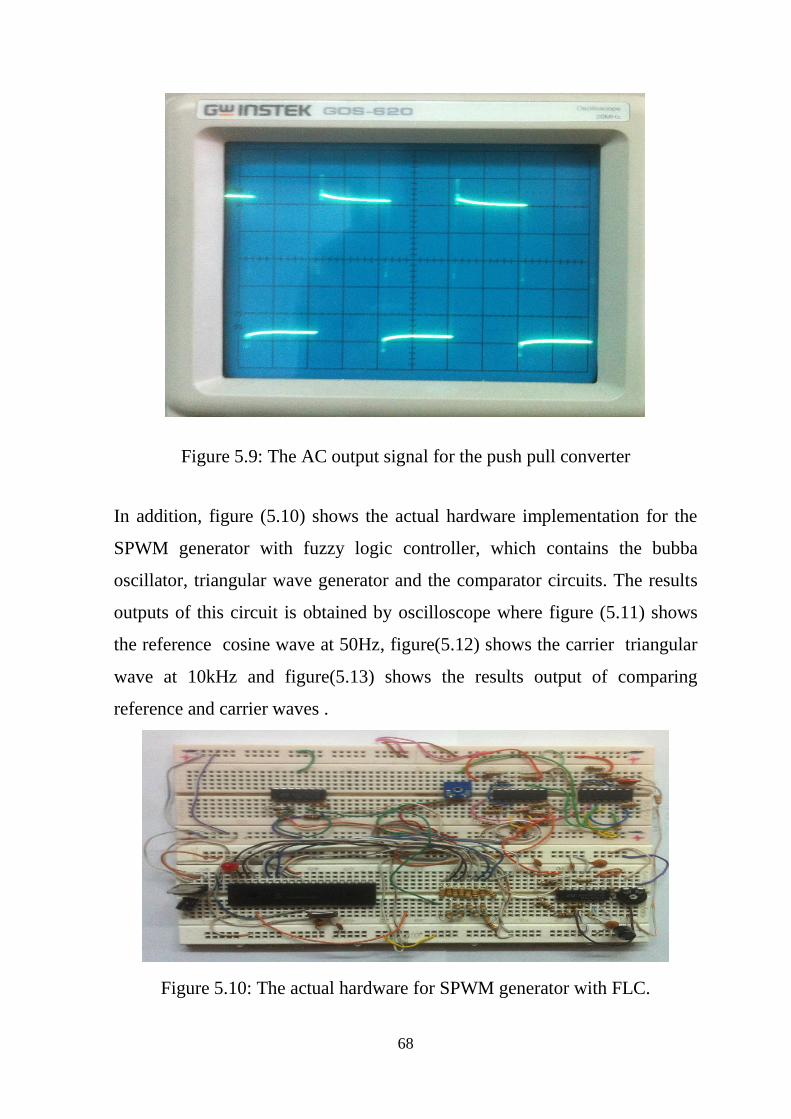
68
Figure 5.9: The AC output signal for the push pull converter
In addition, figure (5.10) shows the actual hardware implementation for the
SPWM generator with fuzzy logic controller, which contains the bubba
oscillator, triangular wave generator and the comparator circuits. The results
outputs of this circuit is obtained by oscilloscope where figure (5.11) shows
the reference cosine wave at 50Hz, figure(5.12) shows the carrier triangular
wave at 10kHz and figure(5.13) shows the results output of comparing
reference and carrier waves .
Figure 5.10: The actual hardware for SPWM generator with FLC.
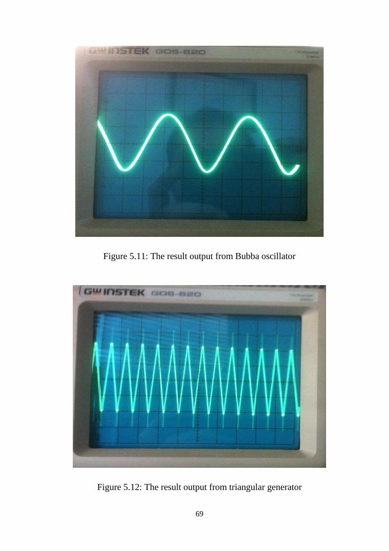
69
Figure 5.11: The result output from Bubba oscillator
Figure 5.12: The result output from triangular generator

70
Figure 5.13: The generated pulses for SPWM generator
Also, figure (5.14) demonstrate the hardware implementation for H-Bridge
with MOSFETS transistor and drivers circuit.
Figure 5.14: H-Bridge and driver circuit

71
5.7 Hardware Results
After collecting all parts of inverter, the new circuit is reconstructed
as shown in figure (5.15) which it is tested under approximated load
at 1KVA. The result output signal is shown in figure (5.16) which it is
almost sine wave signal and having lower harmonic distortion. The
result of RMS output voltage is (216 V), while the error of the output
voltage is (1.8%) for fully loaded inverter. For more detail about the
hardware implementation, refer to appendix C.
Figure 5.15: SPWM full bridge inverter

72
Figure 5.16: The result output signal for full load inverter

73
CHAPTER 6
CONCLUSIONS AND FUTURE WORKS
6.1 Conclusions
Recently, inverters play an important role in various renewable energy
applications where they are used for grid connection of wind energy system
or photovoltaic system. Much progress has been made in successfully
applying FLC in industrial control systems. Dominance of FLC’s over the
conventional controllers has become tight as it can work with imprecise
inputs, can handle nonlinearity and it is more robust than conventional
controllers. FLC techniques represent means of both collecting human
knowledge and expertise and dealing with uncertainties in the process of
control. The following points are accomplished:
1. In this research, the fuzzy logic and classical PI controllers are used for
controlling inverter system as the output voltage is regulated and the
total harmonic distortion (THD) is reduced controlling the modulation
index also. The PWM technique was proposed to generate pure sine
wave with small harmonic distortion .
2. The controllers fuzzy logic and PI were tested by using MATLAB
simulink program and the comparison result shows that the fuzzy logic
controller is the best choice for such application.
3. In this thesis, the controller for proposed system was implemented
using microcontroller PIC16F877A and MICRO C program was used
for programming this microcontroller. The hardware schematic circuits
for all parts of the system was implemented and tested using Proteus
program, which contain push-pull converter, PWM generator, H-bridge
with MOSFET transistors and driver circuit.

74
4. The result of the hardware design implementation of the experiment
almost matched the results that is obtained through simulations.
6.2 Future Works
In this thesis, the fuzzy controller was implemented based on Mamdani
approach for a single phase inverter system, it can be used in other
application such as inductance heating and wilding machine also a good area
for researching are multilevel and three phase inverters .
As future works, this study can be use Sugeno approaches along with
optimization methods in order to reduce the rules of fuzzy controller.

75
References
[1] Sanjay Dixit, Ambreesh Tripathi, Vikas Chola, '' 800VA pure sine wave inverter’s
reference design'' Texas instruments, Application report SLAA602, June 2013.
[2] Ang, Simon S T; Balda, Juan Carlos; Chiacchiarini, Héctor G. “Harmonic distortion
reduction in power inverters” Power Electronics Specialists Conference, IEEE 35th
Annual, Page(s): 1226 - 1231 Vol.2 , June 2004.
[3] Timothy J. Ross, Fuzzy Logic with Engineering Applications, Third Edition, John
Wiley & Sons, Ltd, 2010.
[4] Aleksey Trubitsyn ''high efficiency DC/AC power converter for photovoltaic
application'' Master Thesis, Boston University, 2010.
[5] Rickard Ekström '' Inverter System Design and Control for a Wave Power Substation''
Master Thesis, Uppsala University, 2009.
[6] Keith Jeremy McKenzie ''Eliminating Harmonics in a Cascaded H-Bridges Multilevel
Inverter Using Resultant Theory'' Master thesis, University of Tennessee, Knoxville, 2004.
[7] Robert A. Gannett ''Control strategies for high power four-leg voltages source inverter''
Master Thesis, Blacksburg Virginia, 2001.
[8] Obasohan I. Omozusi '' Dynamics and Control of A Batery Inverter Single-Phase
Induction Generator System'' Master thesis, Tennessee Technological University,
Cookeville, 1998.
[9] Yuqing Tang '' High Power Inverter EMI characterization and Improvement Using
Auxiliary Resonant Snubber Inverter'' Master thesis, Virginia Polytechnic Institute and
State University, Virginia, 1998.
[10] L. Hassaine E. Olías1, M. Haddadi and A. Malek, ''Asymmetric SPWM used in
inverter grid connected'' Revue des Energies Renouvelables Vol. 10 N°3, 421 – 429, 2007.
[11]Surladi ''Analysis Of Harmonic Current Minimization on Power Distribution System
Using Voltage Phase Shifting Concepts '' Master thesis, University of sains Malaysia,2006
[12] T. S. Perry. Lotfi A. Zadeh ,''Fuzzy Logic Inventor Biography '' IEEE Spectrum, pp.
32- 35, June 1995.
[13] L. A. Zadeh. ''Fuzzy sets'', Information and Control, vol. 8, pp. 338-353, Berkeley
California, 1965.

76
[14] E. H. Mamdani and S. Assilian. ''An experiment in linguistic synthesis with a fuzzy
logic controller'' International Journal of Machine Studies, 1975.
[15] S. Yasunobu and S. Miyamoto. ''Automatic train operation by fuzzy predictive
control'' In M. Sugeno, editor, Industrial Applications of Fuzzy Control. North Holland,
1985.
[16] L.X. Wang , A Course in Fuzzy Systems and Controls , Englewood Cliffs, Prentice-
Hall, 1997.
[17] Basil Hamed, Lecture note for fuzzy logic control course, which was taught at Islamic
university of Gaza strip, 2nd semester 2012.
[18] John Yen & Langari Reza, Fuzzy Logic Intelligence Control and Information,
Englwood Cliffs, Prentic-Hall,1999.
[19] Abdul Kareem Z. Mansoor and Ahmed G. Abdullah, ''Analysis and Simulation of
Single Phase Inverter Controlled By Neural Network'' Technical College, Al-Rafidain
Engineering, Vol.20 No. 6, Mosul, 2012.
[20] M. E. Fraser , C. D. Manning "Performance of Average Current Mode Controlled
PWM UPS Inverter with High Crest Factor Load," IEEE Power Electronics and Variable-
Speed Drives, Conference Publication No 399,pp 661-667, 26 - 28 October 1994.
[21] V. Tipsuwanporn A. Charoen , A. Numsomran and K. Phipek4, ''A Single-Phase
PWM Inverter Controlling Base on PLL Technique'' SICE Annual Conference, Waseda
University, Tokyo, Japan 2011.
[22] S. M. Cherati N. A. Azli S. M. Ayob and A. Mortezaei,'' Design of a Current Mode PI
Controller for a Single-phase PWM Inverter'' Power Electronics and Drive Research
Group IEEE, 2011.
[23] N.Karthik, ''Sib Converter with Reduced Harmonic Distortion Using Fuzzy Logic
Controller'' IOSR Journal of Electrical and Electronics Engineering (IOSRJEEE) ISSN:
2278-1676 Volume 2, Issue 1, PP 46-50, July-Aug. 2012.
[24] Ron Mancini and Richard Palmer ''Sine-Wave Oscillator'' Texas instruments,
Application Report SLOA060 - March 2001.

77
VITA
Farok Y. Sharaf has earned his B.Sc. degree in Electrical Engineering from
Islamic University of Gaza on July 2006 and is currently pursuing M.S.
degree in the Electrical Engineering with emphasis in Control Systems. His
research thesis is focusing on re-designing and treating an Electrical
Inverter Systems with Fuzzy Logic Controller for enhancing the
performance and reducing the total harmonic distortion.
Also Mr. Sharaf is currently working as a Director of ElectroSharaf
Company for Electronic Industries since 2006. His future plan is to pursue
his Ph.D. study in Europe in the area of Solar Renewable Energy. Mr.
Sharaf is married with two lovely kids, Yousef and Leen, also he is
enjoying playing sports and reading.

78
APPENDICES
Appendix (A)
Datasheet for Electronics Components

79

80

81

82

83

84

85

86

87
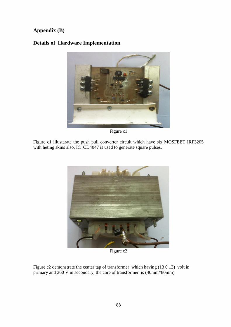
88
Appendix (B)
Details of Hardware Implementation
Figure c1
Figure c1 illustarate the push pull converter circuit which have six MOSFEET IRF3205
with heting skins also, IC CD4047 is used to generate square pulses.
Figure c2
Figure c2 demonstrate the center tap of transformer which having (13 0 13) volt in
primary and 360 V in secondary, the core of transformer is (40mm*80mm)
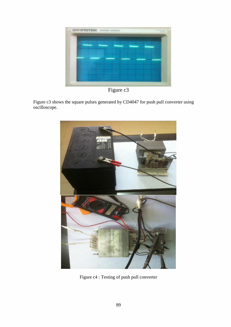
89
Figure c3
Figure c3 shows the square pulses generated by CD4047 for push pull converter using
oscilloscope.
Figure c4 : Testing of push pull converter

90
Figure c5 :Bubba oscillator
Figure c6: Traingulatre carrier generator
Figure c7: comparator circuit for reference and carrier signal

91
Figure c8: Half wave of reference signal
Figure c9: The controller circuit using PIC16F877A
Figure c10: The output pulses generated by PWM generator


![Wind turbine inverter robust loop-shaping control subject ... · a voltage disturbance at the grid to a net change in injected current from the inverter is harmonic admittance [25].](https://static.fdocuments.us/doc/165x107/5f95dee028e1c1260c17f623/wind-turbine-inverter-robust-loop-shaping-control-subject-a-voltage-disturbance.jpg)