Designing MIL Systems that Employ High Speed Data … · Designing MIL Systems that Employ High...
52
Designing MIL Systems that Employ High Speed Data Systems Chris Kendall, CKC Laboratories, Inc. IEEE EMC Rocky Mountain Chapter June 20, 2003
Transcript of Designing MIL Systems that Employ High Speed Data … · Designing MIL Systems that Employ High...
Designing MIL Systems thatEmploy High Speed DataSystems
Chris Kendall,CKC Laboratories, Inc.IEEE EMC Rocky Mountain ChapterJune 20, 2003

©2003 CKC Laboratories Inc.
Past Interference Problems betweenaircraft and cars picture courteously of Mr. Dale Eggen taken by his father

©2003 CKC Laboratories Inc.
Introduction Many new Military designs are employing
high speed data buses DVI, Serdes, Fibre Channel, IEEE 1394 (Firewire), and Ethernet.
MIL-STD-461E, RE102, external limits RS103 at 200 V/m
13,000 V/m may also be imposed.

©2003 CKC Laboratories Inc.
Digital Visual Interface, DVI Stimulate the widespread adoption of
digital displays for high-performancedesktop and mobile PCs
Transition Minimized DifferentialSignaling (TMDS). DVI supports two TMDS links 1.6 GB/sec

©2003 CKC Laboratories Inc.
DVI vs. AnalogDisplay
TypeGraphicsAdapter
SystemOutput
MonitorInterface
DisplayInterface
Analog CRT Digital-to-Analog
Analog Analog Analog
Analog FlatPanel
Digital-to-Analog
Analog Analog-to-Digital
Digital
Digital CRT Digital Digital Digital-to-Analog
Analog
Digital FlatPanel
Digital Digital Digital Digital

©2003 CKC Laboratories Inc.
DVI Properties Risetime = 75 to 140 picoseconds Clock rates Vs. Data rate = 800 MHz/1.6 GHz Amplitudes = 3.3V peak to peak Trace lengths = typical 8 to 12 inches Impedance
100 ohms trace to trace, 50 ohms trace to ground plane
Trace widths = 5 to 8 mils Height above ground = 5 to 8 mils Dielectric constant of PCB = 4.3

©2003 CKC Laboratories Inc.
Predicted Radiated Emissions,PCB (based on EMCad )
Emissions
dBuV/m
Limit
Frequency, Hz

©2003 CKC Laboratories Inc.
Microstrip, for stripline deduct 14 dB Amount of case shielding needed to contain the
PCB emissions Maximum single aperture for –14 dB at 10 GHz
or 0 dB at 5 GHz is about 1.2 inches Maximum single aperture for 36 dB at 800 MHz
is 0.12 inches (Approximately 1/8 inch) Based on 1” yielding 0 dB at 6 GHz.
Predicted Radiated Emissions,PCB (based on EMCad ) Assumptions

©2003 CKC Laboratories Inc.
DVI Cabling Choices Commercial choice is six Twisted shielded
pairs, gross shielded MIL work may use coax and transmit
signal “single ended”. Usually takes two coax cables to equal one
differential pair.

©2003 CKC Laboratories Inc.
Typical commercial DVI Connector Pin-out
Clk -24Hot plug D16No Connect8Clk +23+5 V grd15DDC Data7Clk Shield22+ 5 V pwr14DDC Clock6Data 5+21Data 3+13Data 4+5Data 5-20Data 3-12Data 4-4
0/5 shield191/3 shield112/4 shield3Data 0+18Data 1+10Data 2+2Data 0-17Data 1-9Data 2-1
SignalAssignment
PINSignalAssignment
PINSignalAssignment
PIN
©2003 CKC Laboratories Inc.
Typical DVI CommercialConnector, single link

©2003 CKC Laboratories Inc.
Typical DVI CommercialConnector, single link
DVI/D Dual Link
DVI/D Single Link
DVI/I Analog/Digital
DVI/A Analog

©2003 CKC Laboratories Inc.
Typical DVI Commercial Cable

©2003 CKC Laboratories Inc.
DVI MIL Cable Twinax vs.Quadax
©2003 CKC Laboratories Inc.
DVI Quad Connectors from Gore

©2003 CKC Laboratories Inc.
DVI Quad ConnectorsInserts for size 11 MIL-C-38999 connectors provide optimizedperformance in the smallest possible connector package.
Insert configuration maintains quad geometry through theconnector interface
Improved Z° match minimizes reflections for clean eye patterns
Standard size 22D contacts for high reliability and ease of useSeries 3 coupling provides enhanced EMI performance

©2003 CKC Laboratories Inc.
DVI Signals from coax
Limit
dB uV/m Emissions
Frequency, Hz

©2003 CKC Laboratories Inc.
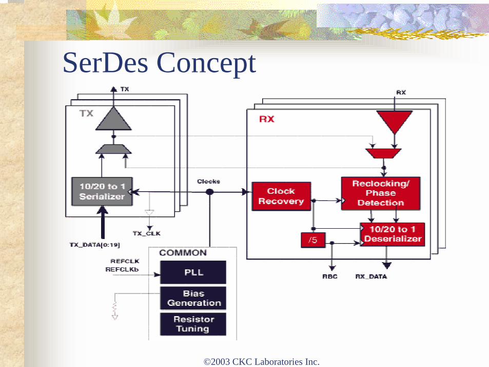
What is SerDes? SerDes stands for serializer/deserializer SerDes typically uses 10 to 1 or 20 to 1 Signal is converted from parallel to serial
©2003 CKC Laboratories Inc.
SerDes Concept

©2003 CKC Laboratories Inc.
What is Firewire? IEEE 1394a"wire" is good for 400 Megabits per
second over 4.5 meters IEEE 1394b extend the rate to 800 - 3200
Megabits over 4.5 meters copper 28 AWG signal pairs with 40 twist/meter, 13 per
foot. Apple = FireWire. Others companies use names,
such as i.link and Lynx

©2003 CKC Laboratories Inc.
Firewire commercial connectors

©2003 CKC Laboratories Inc.
Firewire commercial cable
The Firewire has two

©2003 CKC Laboratories Inc.
IEEE 1394 A EMC Issues Need to DC float connect shell from case
Problem for case shielding Need to AC symmetric shield terminate
shell to case using 1000 pF capacitors Must meet the Lambda/40 rule Must filter the DC lines if used

©2003 CKC Laboratories Inc.
IEEE 1394B Connectors - not thesame as “a”

©2003 CKC Laboratories Inc.
RE102 Emissions from 200 MHz

©2003 CKC Laboratories Inc.
RS103 Hardening requirementsfor firewire
Threshold, dBuV
Frequency, Hz

©2003 CKC Laboratories Inc.
RE102 vs. RS103 Above about 1 GHz, more cable shielding
needed for RS103 than RE102 RS103 > 27 dB @ 200 V/m EME ship > 63 dB @ 13,000 V/m (3-4
GHz)

©2003 CKC Laboratories Inc.
Single-ended high speed Mil designs prefer coax instead of twinax
cables Send high speed singles single-ended
Loose common mode rejection resulting inmore shielding
Typically use transformer to convertdifferential to single-end and back again.

©2003 CKC Laboratories Inc.
DVI Radiated Emission Analysis – Based onEMCad Analysis – SE # 2, Cable Required, Micro-Coax modelUFF092F (100 dB @ 1 GHz)
Center Conductor silver-plated copper
wire
dielectric constant1.4 to 1.7
Silver-plated coppertape – Inner shield
Silver-plated copperwire – outer shield
100 dB @ 1 GHz

©2003 CKC Laboratories Inc.
Internal Flex needed to containHigh Speed Signals
GROUND TRACES
SILVER INKGROUND PLANE
KEVLARINSULATOR
LAYER
OTHER TRACES
DOUBLE SIDEDFLEX CIRCUIT
RELIEFHOLES
KEVLARINSULATOR
LAYER
RELIEF HOLES
SILVER INKGROUND PLANE
©2003 CKC Laboratories Inc.
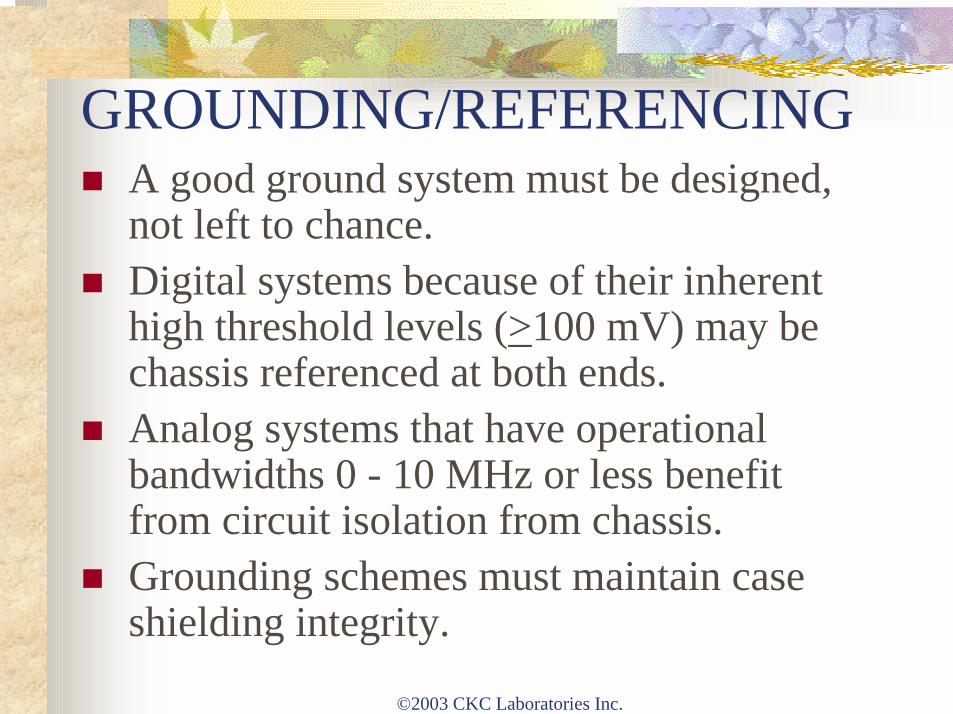
GROUNDING/REFERENCING A good ground system must be designed,
not left to chance. Digital systems because of their inherent
high threshold levels (>100 mV) may bechassis referenced at both ends.
Analog systems that have operationalbandwidths 0 - 10 MHz or less benefitfrom circuit isolation from chassis.
Grounding schemes must maintain caseshielding integrity.

©2003 CKC Laboratories Inc.
GROUNDING/REFERENCING (cont’d.)
• The best approach is a hard reference to chassis at eachunit with the interlacing I/O cable becoming the circuitisolator between same.
• The exception to this rule would be for analog or signaling circuits which cannot be easily isolated by acommon inductance between the center conductor andits return.
• However, leaving a ground system to be developed byeach design entity is not recommended.

©2003 CKC Laboratories Inc.
SINGLE POINT ORREFERENCE CONCEPTSingle point grounding
cannot existNo dimensions,therefore no wayto terminate wirestogether
Ground reference areaof diameter “D”I x Zd = ∆Vthat is below allcircuit threshold valuesreferenced to ground.
Point
D
BW = =1πtr
300 MHztr nsecs
∆VZd
ITotal

©2003 CKC Laboratories Inc.
SEPARATE GROUNDS SHOULDBE USED FOR LOWFREQUENCY CIRCUITS (<1MHz)
* AC power ground (green wire) should be connected tohardware ground (within 1.5 inches of case entry)
SignalGround
NoisyGround
HardwareGround*
distributed capacitancebetween “ground”leads
distributed mutualinductance between“ground” leads

©2003 CKC Laboratories Inc.
SINGLE POINTGROUNDS
Signal CurrentLoop Control?
Signal CurrentLoop Control?
1A. Series
1B. Parallel
1 2 3
1 2 3
I1 I2 I3
I3I2 +I3I1 + I2 +I3

©2003 CKC Laboratories Inc.
SINGLE POINT GROUNDS
Loop Control?
1A. Series
1 2 3
Loop Control?
1B. Parallel
1 2 3

©2003 CKC Laboratories Inc.
POOR SINGLE REFERENCE GROUNDINGBECAUSE OF LARGE EXPOSED LOOP AREAS
InputSignals
InputSignalConversionandFiltering
ConditionedSignal
ControlLogic
LogicGround
OutputSignals
Output Ground
ToDCInput
No Decouplingof Logic Groundat Port of Exit
LogicPackagingGround
ToCabinet
AC Power LineSGP Power Supply Ground
AC PowerFilter
Logic PowerSupply
DC OutputPower Supply
Filtered Power
OutputDrivers
Input Ground
Filter Ground

©2003 CKC Laboratories Inc.
POOR SINGLE REFERENCEGROUNDING This viewgraph was taken from literature
and was titled "The Proper Way toGround". One can see that the conditioned signals
transferring from the input conversionto the control logic could not possiblybe transmitted if the only signal returnwas through the single ground point(SGP).
This is because each of the 3 linesshown would form 3 concentric loopareas that would crosstalk.

©2003 CKC Laboratories Inc.
PROPER APPLICATION OFTRANSMISSION LINES TOSINGLE-ENDED CIRCUITSBad
No ShieldLarge Enclosed Area
Preferred
Shield AreaBoth Ends of Chassis
Grounded - SignificantReduction in Loop Area
Bad
Shield AddedOne End ChassisGrounded - NoReduction inLoop Area

©2003 CKC Laboratories Inc.
EFFECT OF SHIELD ON LOOP AREA
VS RL
I
VS RL
I
VS RL
I
f< Rs2πLs
VSRL
I
f> 5Rs2πLs R
I1
Is = I1
No GroundConnections
Shield AddedTwo Ends Grounded
Large Area
Shield AddedOne End Grounded
Large Enclosed Area
No ShieldLarge Enclosed Area
Circuit Not GroundedAt One EndReduced Area
Shield AddedTwo Ends Ground
Reduced AreaNotes:Rs = Shield ResistanceLs = Self Inductance of Shield
f (cut-off) =or 2πf =ωc =
Rs2πLs
RsLs
RsLs

©2003 CKC Laboratories Inc.
MEASURED VALUES OF SHIELD CUT-OFFFREQUENCY (FC)
CABLEIMPEDANCE
(ΩΩΩΩ)
CUT-OFFFREQUENCY
(kHz)
FIVE TIMESCUT-OFF FREQUENCY
(kHz) REMARKS
Coaxial Cable
RG-6ARG-213RG-214RG-62ARG-59CRG-58C
755050937550
0.60.70.71.51.62.0
3.03.53.57.58.010.0
Double Shielded
Double Shielded
Shielded Twisted Pair
754E24Ga.22Ga.1
125------
0.82.27.0
4.011.035.0
Double Shielded
Aluminum-FoilShield
Shielded Single
24Ga. --- 4.0 20.0
1 One pair out of an 11 pair cable (Belden 8775).
From: “Noise Reduction Techniques in Electronic Systems”, by H.W. Ott, 2nd ed.(1988) by Bell Telephone Laboratories Inc., Reprinted by permission of JohnWiley & Sons, Inc.

©2003 CKC Laboratories Inc.
DIVISION OF CURRENT BETWEEN SHIELDAND GROUND PLANE
Subscript SH = ShieldMesh Equation Inside Loop
For ω >> ωc 0 = IS (jωLS + RL) - ISH (jωm)
IS = ISH ( ) = ( ) ISH
At ω >> ωc all current returns on shieldAt ω <<ωc all current returns through ground
jωjω + RS/LS
jωjω + ωc
IS ISH IS
IG
B A
IG = IS - ISH
ωc =RLLS
IS
RL
ISH IG
LS
m
B A

©2003 CKC Laboratories Inc.
GROUND LOOPIf shielded current is allowed to flow and the shield is one of the signalconductors, a noise voltage will be generated due to the I-R drop in the shield.
V12 = -jωMIS + jωLS IS + RS IS
Since M = LS (self inductance)Then V12 = RS IS
Therefore: Avoid shield being a signal conductor1. Use shielded twisted pair2. Use triaxial cables3. At high frequencies (>1 MHz) coax acts as triax due to skin effects
Low frequency
RS
Shield
Center Conductor
MVCRT
Vs
R
1
2
IS

©2003 CKC Laboratories Inc.
GROUNDING SCHEMES Subdivide as follows:
AC power grounding: safety
DC power distribution: 3.3V, +5, + 12V, etc.
Signal reference
Analog
Digital
Discrete
Video
AC power green/yellow isolated from DC by transformer DC power isolated from signal in transmission bandwidth by
transmission line effect of interconnect cable (i.e., coax, twisted pair,tri-lead, GSG ribbon cable, or 3M style ground plane ribbon cable

©2003 CKC Laboratories Inc.
COAX AS GROUND LOOP SUPPRESSOR
Common made currentlimited by mutualinductance of COAX
Ic
2nd unit PCBPower
Distribution
Coax CableIsolationof Signals
DC Power
PC BoardPower
Distribution/ / / /
/ // /

©2003 CKC Laboratories Inc.
COAX AS GROUND LOOPSUPPRESSOR
This is a schematic of the isolationachievable through the signal cable. The common mode current IC is
inhibited by the mutual inductance,hence the isolation quality of thecoax signal cable.

©2003 CKC Laboratories Inc.
GROUND PLANE IMPEDANCE
Total Impedance Consists of:1. DC resistance2. Inductance effect3. Skin effect4. Standing wave impedance
(transmission line effect)
Copper
Area = A
B
t
©2003 CKC Laboratories Inc.
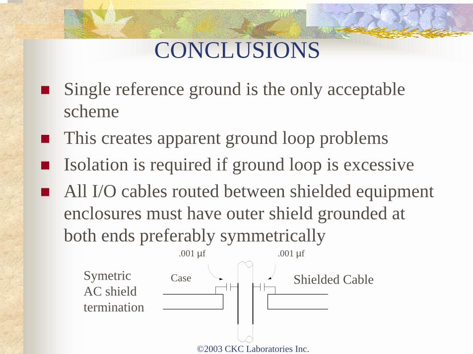
CONCLUSIONS Single reference ground is the only acceptable
scheme This creates apparent ground loop problems Isolation is required if ground loop is excessive All I/O cables routed between shielded equipment
enclosures must have outer shield grounded atboth ends preferably symmetrically
.001 µf.001 µf
Case Shielded CableSymetricAC shield termination

©2003 CKC Laboratories Inc.
ISOLATION SCHEMES Differential Circuits Optic Couplers Isolation Transformers Coax Cables and/or Twisted Shielded Pair Fiber Optics Except for the last two schemes, the above
concepts do not work for controllingemissions or rejecting ESD and E-Fieldradiation.

©2003 CKC Laboratories Inc.
DIFFERENTIAL DRIVERS
Good to about 5 MHz (i.e. >20dB).Cause of high frequency common reduction is:1. Unbalance in common mode Z in high frequency.2. Unbalance in connectors.3. Unbalance in twisted pairs in internal route.4. Unbalance in PC board traces.5. Unbalance in twisted shielded pairs.Radiation from differential drivers is 2X single ended
drivers (line to ground).Major external threat is 5-200 MHz range where
common mode isolation is least.
Line Z 1
Line Z 2V2
V1
Frequency
Com
mon
Mod
e R
ejec
t.
100 kHz
~ 80 dB
~ 10 dB to0 dB
-20 to -40 dB/D
H
L

©2003 CKC Laboratories Inc.
OPTIC ISOLATORS
MutualCouple
1. Isolation limited by harness and connector coupling2. To work without external cable shield they need to be located within 1.5" of case entry3. If used, then need separate PC board connectors
Re-radiatedE-Field
To motherboardconnector

©2003 CKC Laboratories Inc.
Tomahawk Cruise Missile Changes allows
programming inminutes today
Future: allowprogramming in flight
May need greatbandwidth toaccomplish