
DesignCon 2016 - Samtec Microelectronicssuddendocs.samtec.com/notesandwhitepapers/designcon2016...of...
16
DesignCon 2016 Microwave Interconnect Testing For 12G-SDI Applications Jim Nadolny, Samtec [email protected] Corey Kimble, Craig Rapp – Samtec OJ Danzy, Mike Resso – Keysight Boris Nevelev – Imagine Communications
Transcript of DesignCon 2016 - Samtec Microelectronicssuddendocs.samtec.com/notesandwhitepapers/designcon2016...of...

DesignCon 2016
Microwave Interconnect Testing
For 12G-SDI Applications
Jim Nadolny, Samtec
Corey Kimble, Craig Rapp – Samtec
OJ Danzy, Mike Resso – Keysight
Boris Nevelev – Imagine Communications

Abstract
SMPTE ST 2082-1:2015 is the current standard for high-speed digital video and requires
testing to 12 GHz for video connectors. Off-the-shelf test solutions exist for some types
of cable connectors but are lacking for board mount video interconnect. A method to
reliably de-embed PCB effects, bifurcate mated connector S-parameters and trade-offs
associated with the location of the 50-75 ohm transition are presented. To provide
context, the evolution of video signal bandwidth and the legacy issues surrounding video
transport are addressed.
Author(s) Biography
Jim Nadolny received his BSEE from the University of Connecticut in 1984 and an
MSEE from the University of New Mexico in 1992. He began his career focused on EMI
design and analysis at the system and component levels for military and commercial
platforms. For the last 15 years his focus has shifted to signal integrity analysis of multi-
gigabit data transmission systems.
Acknowledgements
Significant contributions to this research included my colleagues from Samtec, Corey
Kimble, Craig Rapp, David Blankenship and Chris Shelly. Boris Nevelev from Imagine
Communications provided insight to the video broadcast industry as well as technical
requirements above and beyond those defined in the SMPTE specification. Finally OJ
Danzy and Mike Resso contributed on the proper use of PLTS, AFR and related
instrumentation details.

1. Introduction
Streaming HD video and Ultra HD 4K television are just 2 examples of a continuing
evolution in video signaling. Video has transformed from being an analog 6 MHz
bandwidth signal to a 12 Gb/s digital data stream. As the signaling transitioned into the
digital domain, first at SD and the HD formats, and, recently at 6Gb/s and 12Gb/s 4K
UHD-SDI standards, the demand for meeting stringent return loss requirements up to
12GHz has emerged.
In this paper, we will address several aspects of video interconnect testing. First, we will
look briefly at the evolution of video transmission and industry standards for context in
what is driving electrical requirements for interconnect components. Next, we will
consider interconnect test methods that are readily used but have shortcomings. Finally,
we will show an improved test method which makes use of de-embedding and reference
impedance transformation.
2. Evolution of Video Transmission
Consumer demand for higher quality video and on-demand services summarizes an
ongoing trend that industry is responding to with enhanced products. Historically,
television required 6 MHz of bandwidth which was transmitted over 12 channels in the
VHF band. Today, “television” has been replaced with hundreds of digitized, on demand
video services. In between has been a continuing progression of higher quality
equipment and services.
At the consumer level, High Definition Media Interface (HDMI) and Display Port are
typical interfaces to display devices such as TVs, projectors and monitors. At the
commercial level, Serial Digital Interface (SDI) is the dominant interface for broadcast
video which is governed by the Society of Motion Picture and Television Engineers
(SMPTE). Broadcast video is the term used for the distribution of video over satellite,
cable and terrestrial infrastructure.
The SDI specification defines unbalanced digital signals in a 75 ohm coaxial cable
environment. This is in contrast to telecom standards (such as Ethernet) which transmit
similar high-speed digital signals but use a 100 ohm differential twinax cable plant or
fiber optic interconnects. In both Ethernet and broadcast video, signal quality and port
density are product differentiators.
Figure 1 shows an example of broadcast video port density. Figure 2 shows the coaxial
cable plant associated with these installations. These photos help illustrate the extreme
port density and need for higher density panel connection solutions.
With this as an introduction to broadcast video, we now turn our attention to the electrical
performance requirements for these coaxial components, and how to test them.

Figure 1. Broadcast Video Equipment Port Density
(Courtesy of Imagine Communications)
Figure 2. Broadcast Video Cable Plant
(Courtesy of Imagine Communications)

3. Electrical Performance Requirements
SMPTE ST 2082-1:2015[1] describes the electrical and physical characteristics of a 12G-
SDI coaxial cable interface. Digital signal characteristics (jitter, amplitude, overshoot
and rise/fall times) for the transmitter are defined and a channel loss of up to 40 dB at one
half the clock frequency (6 GHz) is assumed for the interconnect channel. Receiver
characteristics are specified only in that they must operate with the assumed cable loss
and transmitter characteristics.
The specification for the coaxial connectors and cables are straightforward. The return
loss of the generator and receiver circuit, including the connector, shall meet or exceed
the specification shown in Figure 3. The connectors and cables combined shall have an
attenuation curve that follows a 1 √𝑓⁄ relationship. This implies that the insertion loss of
the interconnect should be dominated by attenuation and the return loss component in the
channel is “small”.
Figure 3. SMPTE ST 2082-1:2015 Connector Return Loss

While not specified in SMPTE ST 2082-1:2015[1] isolation is very much a requirement
in broadcast video. We can deduce from the specification that typical video broadcast
channels can have 40 dB of insertion loss at 6 GHz. This would imply that the total
isolation from all aggressors combined needs to be more than 40 dB worst case for a
practical signal-to-noise ratio. More isolation is better, of course, but recognize that these
are single-ended channels that do not benefit from common mode rejection which is a
major benefit in differential systems.
Figure 4 shows a fairly typical isolation profile for board mount BNC connectors.
Isolation was not a design objective in this test fixture, rather the focus was on optimizing
the footprint for minimal reflections. The board uses microstrip trace routing and even
though there is more than 0.5 inches of separation between video traces, only 35 dB of
isolation is achieved at 4.6 GHz. Stripline or Coplanar Waveguide routing with isolation
vias are common design techniques required to increase the level of isolation.
Figure 4. Typical Isolation with Board Mount BNC Connectors
4. Legacy Component Test Methods
Return loss testing of 75 ohm video connectors is a mature field, but somewhat limited in
scope. It is mature in that 75 ohm calibration kits and precision adapters are generally
available for popular connector series (Type F, N and BNC). Limited in scope refers to
the relatively limited supply of calibration kits/adapters with a 12 GHz bandwidth. These
challenges translate into higher test costs, but are surmountable.
Recall that the intent of SMPTE ST 2082-1:2015 is to provide an attenuation curve that
follows a 1 √𝑓⁄ insertion loss profile. This means that all reflections in the channel must
be “small”, and this applies to the connector to PCB transition. The transmitter and
receiver circuitry is packaged on a PCB, and the video signal is fed to this circuitry via
controlled impedance stripline/microstrip transmission lines. This coax to stripline
reflection must also be “small” and needs to be included as part of the PCB mount video
connector test.
One legacy method of measuring return loss of embedded structures is time domain
gating. Time domain gating is a feature on modern network analyzers which allows one

to shift the measurement reference plane and replace structures that are not of interest.
While this method is simple and easy to apply, there are two significant shortcomings.
First, placement of the gates (reference planes) tends to be imprecise and dependent on
the operators “feeling” of where they should be located. This leads to a lack of
repeatability, but with careful time/feature based definitions, the gate placement can be
controlled. Since the gate placements are subjective, it is possible to violate the central
requirement of gate location relative to a discontinuity. The response resolution curve in
Figure 5 is helpful in defining how close a gate can be placed to a discontinuity. For a
typical 12G-SDI BNC PCB mount connector, a test bandwidth of 20 GHz is required to
locate the gate within 20 ps of the discontinuity.
Figure 5. Response Resolution for Time Domain Gating
The second shortcoming of time domain gating is that only reflection parameters can be
easily obtained using this technique. While the return loss can be obtained, the
transmission terms (insertion loss and crosstalk) of the S-parameter matrix are not
modified with the placement of a gate on a reflection parameter. This can be problematic
when comparing measured data to simulations of the connector and footprint.
Finally, gating does not remove the electrical length of the section that is selected. The
section that is removed is replaced with either an ideal transmission line in the
characteristic impedance of the system, or a modeled line with start and stop impedances
of the placement of the beginning and end gates [2].

Other techniques for compensating for the impedance difference are the use of minimum
loss pads and automatic port extensions. Both of these techniques have other pros and
cons that are discussed in further detail in [3].
PCB Complications
One of the greatest challenges to complying with the return loss requirements of 12G-
SDI is engineering the BNC to PCB interface. This is referred to as the connector
footprint and is typically optimized using full wave simulation tools. This optimization is
specific to a particular PCB stackup and material set. Parameters that are optimized
include pad size, anti-pad size, drill size and backdrilling depth. Figure 6 shows a 75
ohm BNC7T connector mounted to a multilayer PCB and the detail associated with the
footprint parameters. Simulation times for these structures are typically 2 hours or less;
however, building the model can be a tedious task, taking a day to complete.
Figure 6. 12G SDI BNC Connector Optimization
Given that the connector footprint design is a critical and tedious effort, validation via
test is imperative. A test method which places the measurement reference plane at the
separable coaxial interface and the 2nd reference plane within several hundred mils of the
connector footprint is required. Figure 7 illustrates the ideal reference plane location.
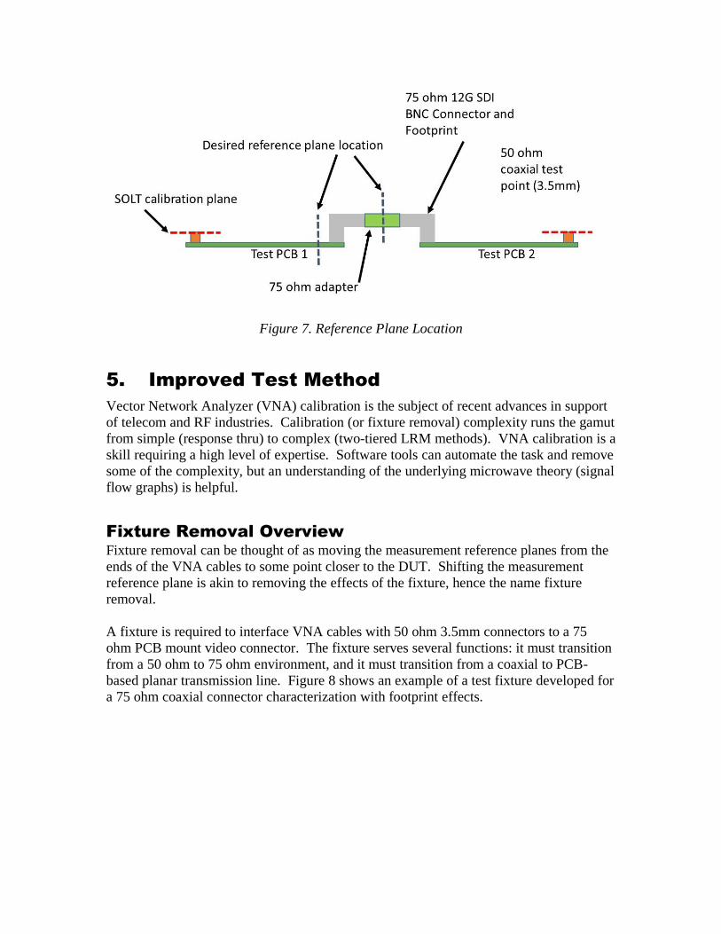
Figure 7. Reference Plane Location
5. Improved Test Method
Vector Network Analyzer (VNA) calibration is the subject of recent advances in support
of telecom and RF industries. Calibration (or fixture removal) complexity runs the gamut
from simple (response thru) to complex (two-tiered LRM methods). VNA calibration is a
skill requiring a high level of expertise. Software tools can automate the task and remove
some of the complexity, but an understanding of the underlying microwave theory (signal
flow graphs) is helpful.
Fixture Removal Overview
Fixture removal can be thought of as moving the measurement reference planes from the
ends of the VNA cables to some point closer to the DUT. Shifting the measurement
reference plane is akin to removing the effects of the fixture, hence the name fixture
removal.
A fixture is required to interface VNA cables with 50 ohm 3.5mm connectors to a 75
ohm PCB mount video connector. The fixture serves several functions: it must transition
from a 50 ohm to 75 ohm environment, and it must transition from a coaxial to PCB-
based planar transmission line. Figure 8 shows an example of a test fixture developed for
a 75 ohm coaxial connector characterization with footprint effects.

Figure 8. 12G-SDI Test Fixture for 75 ohm BNC
Fixture removal begins with a traditional calibration of the VNA using 50 ohm
mechanical calibration standards. This sets the reference plane at the end of the VNA test
cables. The next step is characterizing one or several PCB based calibration standards
with known characteristics. From these characterizations of known elements, an accurate
model of the test fixture can be created. The model of the test fixture is described
mathematically in terms of S-parameters. Next, the 75 ohm BNC connector is measured
with the test fixture included. At this point, all the necessary measurements have been
completed. The final step is de-embedding the test fixture using microwave network
theory. The S-parameters of both measurements are first transformed to a slightly
different format known as transfer scattering parameters. By inverting the fixture transfer
scattering matrix and multiplying with the overall transfer scattering parameter, the
fixture effect is removed. The final step is transforming the transfer scattering parameter
back to an S-parameter matrix and plotting the result. In practice, the matrix math is
automated in the software tools that support the VNAs.
The benefits of this test method over time domain gating are significant. The method is
repeatable and not subject to the estimation of best gate location. The result is an S-
parameter representation of the connector and footprint which includes transmission
terms. This measured data can be used in channel level simulations or to validate models
generated from full wave simulation.

Fixture Design
The fixture design is best done in concert with the footprint optimization process. As
explained earlier, the footprint optimization is unique to the PCB stackup. A
complication associated with 12G-SDI is the need for a 50 ohm to 75 ohm transition in
the trace impedance. The 75 ohm requirement comes from the need to match the 75 ohm
BNC connector while the 50 ohm requirement is necessary to match the 50 ohm coaxial
test point. The approach is to start with a stackup that can yield a 75 ohm impedance
with a manufacturable trace width (typically 4 -5 mils). An example test fixture stackup
is shown in Figure 9. The trace impedance transitions to 50 ohms by increasing the trace
width. Figure 10 illustrates the concept.
Figure 9. Test Fixture Stackup
Figure 10. 12G-SDI BNC Connector Test Fixture
Additional features can be added to the test fixture depending on the information
required. For example, multiple connectors can be placed next to each other for crosstalk
investigations.

Calibration Standards Design
The purpose of the calibration standard is to exactly mimic the portion of the test fixture
that is to be de-embedded. This mandates that the calibration standard is fabricated from
the same PCB panel as the test fixture. By replicating the material parameters and
manufacturing process, the calibration standard will have the same electrical properties
(impedance, group velocity, dispersion) as the test fixture.
There are several de-embedding algorithms which can be used for fixture removal and
the calibration standard design is customized for the algorithm. In this effort, the
Keysight Automatic Fixture Removal (AFR) method is used, in part because of the very
simple calibration standards required. A single 2X through standard is all that is
required.
The calibration standard defines the reference plane location and shifts it from the surface
of the coaxial test point to the 75 ohm feed near the 75 ohm BNC connector (refer to
Figure 10). For AFR, this calibration standard is referred to as a “2X thru calibration
standard” and is illustrated in Figure 11. Note that the length of the 75 ohm section is
fairly short (65 mils) in this example. The intent is to minimize the reflection loss of this
discontinuity, however this locates the reference plane very close to the BNC connector
footprint. If the reference plane is too close to the discontinuities associated with the
footprint, evanescent modes exist at the reference plane, which introduces errors.
Locating the reference plane 50 mils from the footprint discontinuity is a reasonable
trade-off between the competing goals.
Figure 11. 2X Thru Calibration Standard

Test Process
The test process begins with either an SOLT or eCal of the VNA at the coaxial test ports.
These are routine calibrations and form the first tier of the two-tier calibration process.
After SOLT calibration, the 2X thru calibration standard is measured and the BNC
connector plus test fixture is measured. These results can be stored in either a VNA
native format or in Touchstone format.
The next step is to create the test fixture model using the AFR algorithm within the VNA
control software package Keysight Physical Layer Test System (PLTS). The process is
menu driven and intuitive; however, care should be taken to set the calibration reference
impedance to 75 ohms. The 2X thru fixture is effectively bifurcated into 2 symmetrical
1X thru test fixtures which can be used in the subsequent step.
The connector and test fixture response is loaded and the 1X thru test fixture can now be
de-embedded. Within the AFR environment, this is the “remove fixture” step. Next is
exporting the data and setting the reference impedance to 75 ohms. Setting the reference
impedance of the Touchstone 1.1 file can be done either within PLTS or by editing the
control line of the exported Touchstone 1.1 file. If the tool that will be consuming the
data supports the use of Touchstone 2.0, a file can be exported in that format where the
input and output impedances of each port can be properly represented.
Bifurcation
There is one final step required to obtain the Touchstone model for a single connector
and footprint. We want to bifurcate the de-embedded test data so that we have the
response of only the 12G-SDI connector, coaxial mating interface and footprint. This is
done by invoking the AFR algorithm for 1X fixture creation from a 2X thru calibration
structure. In effect, the connector response is divided in half, or bifurcated.
This step can only be applied to symmetrical configurations and is illustrated in Figure
12. In some cases, two 2X thru structures or one 2X thru structure and a 1X reflect
structure for one side can also be used when the two halves of the fixture do not have the
same electrical length.

Figure 12. Bifurcation Process
Test Results
The approach outlined in this paper intentionally introduces a 50 ohm to 75 ohm
discontinuity with the 2X thru calibration standard. In general, this is a practice to be
avoided as it reduces the effective bandwidth of the measurement. A simple way to
check the maximum bandwidth of the calibration is to compare the return loss and the
insertion loss of the 2X thru calibration standard. Ideally, there should be at least 5 dB
separation between the two curves. When these two curves cross, the calibration
algorithm will no longer be valid. Figure 13 shows the insertion loss and return loss of
the 2X thru. We see two regions near 16 GHz and 19 GHz where the 5 dB separation
guideline is violated; however, the 0 dB requirement is not.
Figure 13. 2X Thru Calibration Standard
In Figure 8, the 75 ohm edge mount connector and test fixture is shown. During test, the
initial measurement includes the test fixture, two 75 ohm edge mount BNC connectors
and a precision 75 ohm adapter which is inserted between the 2 BNCs. The insertion loss
and return loss of this entire structure is shown in Figure 14. Note that this structure has
50 ohm test board traces and 75 ohm BNC connectors, so a high level of reflection loss is
expected. This is the case with the return loss of 7.5 dB at 1.06 GHz.

Figure 14. 75Ω Connectors, Adapter and 50Ω Test Fixture
Applying the AFR de-embedding algorithm removes the test fixture. This is a menu
driven operation within PLTS and the software checks for 2X thru symmetry, a
requirement for successful de-embedding. Figure 15 shows the result of de-embedding
the test fixture. Notice that the insertion loss is improved as the PCB trace loss has been
removed. Also notice the improved low frequency return loss due to the removal of the
50 ohm to 75 ohm discontinuity.
Figure 15. 75Ω Connectors and Adapter
The final step uses the AFR algorithm to bifurcate the results shown in Figure 15 to
obtain the S-parameters of a single edge mount 75 ohm connector, its footprint and the
mating interface to the coaxial adapter. The results shown in Figure 15 are effectively
treated as a 2X thru test fixture in AFR. The AFR algorithm bifurcates the structures and
the 1X “fixture” can be exported. The result is shown in Figure 16. The return loss
requirements of SMPTE ST 2082-1:2015 are also plotted in red for reference in Figure
16.

Figure 16. 75Ω Connector
6. Conclusions
Validation of video connectors for 12G-SDI applications has several challenges. The
impedance difference between instrumentation (50Ω) and video cables and connectors
(75Ω) is one. Second, the availability of precision adapters can be problematic. Finally,
a more significant challenge is including footprint effects in the measured connector
response. A method has been shown using modern de-embedding algorithms to include
the footprint and bifurcate a mated connector pair to obtain the results for an individual
BNC.
7. References
[1] SMPTE ST 2082-1:2015 12Gb/s Signal/Data Serial Interface – Electrical
[2] “Time Domain Analysis with a Network Analyzer”, Keysight Application Note 1287-
12
[3] J. Ferry, “Characterizing Non-Standard Impedance Channels with 50 Ohm
Instruments”, DesignCon 2009