DesignCon 2014 - Xilinx · 2019-10-14 · DesignCon 2014 Touchstone® v2.0 SI/PI S- Parameter...
18
DesignCon 2014 Touchstone ® v2.0 SI/PI S- Parameter Models for Simultaneous Switching Noise (SSN) Analysis of DDR4 Memory Interface Applications. Romi Mayder, Xilinx, Inc. [email protected] Raymond Anderson, Xilinx, Inc. [email protected] Nilesh Kamdar, Agilent Technologies [email protected]
Transcript of DesignCon 2014 - Xilinx · 2019-10-14 · DesignCon 2014 Touchstone® v2.0 SI/PI S- Parameter...
DesignCon 2014
Touchstone® v2.0 SI/PI S-
Parameter Models for
Simultaneous Switching Noise
(SSN) Analysis of DDR4
Memory Interface Applications.
Romi Mayder, Xilinx, Inc.
Raymond Anderson, Xilinx, Inc.
Nilesh Kamdar, Agilent Technologies
Abstract
Large port count (>100) Touchstone® v2.0 S-Parameter data formats with per port
reference impedances are essential in designing the next generation of memory
interconnects. Using DDR4 as an example this paper shows how Touchstone v1.0 format
limitations can lead to erroneous or inaccurate results for SI and PI co-simulations and
how they can be overcome using the new v2.0 format. In addition to reliable channel
models, one also needs accurate representation of the memory controllers and memory
modules. To simulate SSN, Power Aware IBIS v5.0 models are required. This paper will
demonstrate the accuracy and efficiency of such models by examining a few examples.
These models, combined with the interconnect models, can then be used in a transient
(SPICE) simulator to analyze SSN and its effects on the design. Such an analysis allows
one to identify problem areas, debug issues and optimize the design to meet
specifications in a timely manner.
Author(s) Biography
Romi Mayder is currently the Senior Manager of Transceivers and IOs in the Technical
Marketing Department at Xilinx, Inc. Prior to joining Xilinx, Mr. Mayder worked as a
consultant specializing in silicon die level signal and power integrity. He also consulted
in the field of design and fabrication of advanced package technologies, including
stacked silicon interconnect. Mr. Mayder has been employed by two companies in the
Test and Measurement industry, Agilent Technologies and Anritsu (Wiltron) Company,
where he specialized in microwave and millimeter wave microelectronic circuit design
and fabrication. Additionally, Mr. Mayder has over 10 years of experience in
semiconductor process technologies including photolithography, ion implantation,
plasma enhanced chemical vapor deposition, dielectric sputtering, and chemical
mechanical polishing of silicon wafers. Mr. Mayder received his Bachelor of Science
degree in Electrical Engineering and Computer Science from the University of California
at Berkeley in 1992. Mr. Mayder has published 25 patent applications in the fields of
signal and power integrity as well as semiconductor process technologies.
Raymond Anderson is Senior Signal Integrity Staff Engineer at Xilinx. His current
activities include package development and modeling and simulation of high-speed IO
and power distribution networks for FPGAs. He holds a BSCS degree from National
University. Prior to his current Xilinx position he has held positions at California
Microwave, Equatorial Communications, GTE Spacenet and Sun Microsystems. His
background includes microwave amplifier design, development of satcom ground station
systems, CAD software development and both PCB and package level signal integrity
work. He has published 5 signal integrity related papers at various IEEE conferences and
holds 8 patents in the signal integrity field.
Nilesh Kamdar is Senior Applications Engineer at Agilent Technologies. He has over 14
years of experience working on high frequency and high speed digital design. Mr.
Kamdar managed the Simulation Architecture team at Agilent EEsof in his previous role.
He received his Masters of Science degree in Electrical Engineering from Utah State
University in 1999.
1 Touchstone v2.0
1.1 Overview
In order to accurately simulate the performance of modern systems utilizing high-speed
memory interfaces such as DDR4 it is essential to capture not only the standalone
performance of the transmission lines and PDNs, but to utilize models that accurately
capture the coupling effects between the transmission lines and the associated PDNs. In
the case of DDR4 interconnects, beside the multiple bytes of the data lanes, clock,
address and control nets, may be models of the power distribution nets. Of particular
import is the coupling between the PDN and the signal lines.
In simulating signaling portion of the DDR4 memory interface, some of the various
effects that may degrade the performance are reflections, inter-symbol interference (ISI),
crosstalk (NEXT and FEXT) and SSN noise. These effects distort the transmitted and
received data bits traveling through the system and lead to the degradation of the eye-
diagram opening. Of the four effects just mentioned, the generation of SSN noise is most
directly influenced by PDN performance. To perform accurate electrical simulations that
capture the effects of both the signal lines and the PDN it is necessary to generate a S-
Parameter model that has data for both the signal lines and PDN in the same file, i.e. a
true SI/PI model. If the S-Parameters are in separate files as a result of separate
extractions, the critical coupling between the signals nets and the PDN will not be
captured.
The requirement that the signal, and PDN net S-Parameters, be in the same Touchstone
file brings up another interesting issue: We require the signal nets normalized to 50 ohms
and the PDN nets normalized to 0.1 ohms. In order to perform accurate simulations, it has
been found that it is usually necessary to have the S-Parameters normalized to an
impedance somewhat near to the impedance of the relevant nets. (DDR4 signal lines
typically have a characteristic impedance of around 40 ohms. PDNs are low impedance
structures whose impedance varies from a few milliohms to a few ohms.) The reason
behind this is the fact that when the magnitude of an S-Parameter gets to be very close to
+/-1 (as is the case when the impedance of a structure is far from the normalization
impedance) one encounters numerical issues in simulators due to numerical noise.
The two Smith Charts shown in Figure 1 have the same S-Parameters plotted on each
one. The data extends from DC to 1000 MHz. In the left-side chart the S-Parameters
were normalized to 0.1 ohms. In the right-side chart the same S-Parameters were
normalized to 50 ohms. The data normalized to 50 ohms is compressed around the origin
(chart center) and along the edge of the chart. The data normalized to 0.1 ohms is well
spread out on the chart.
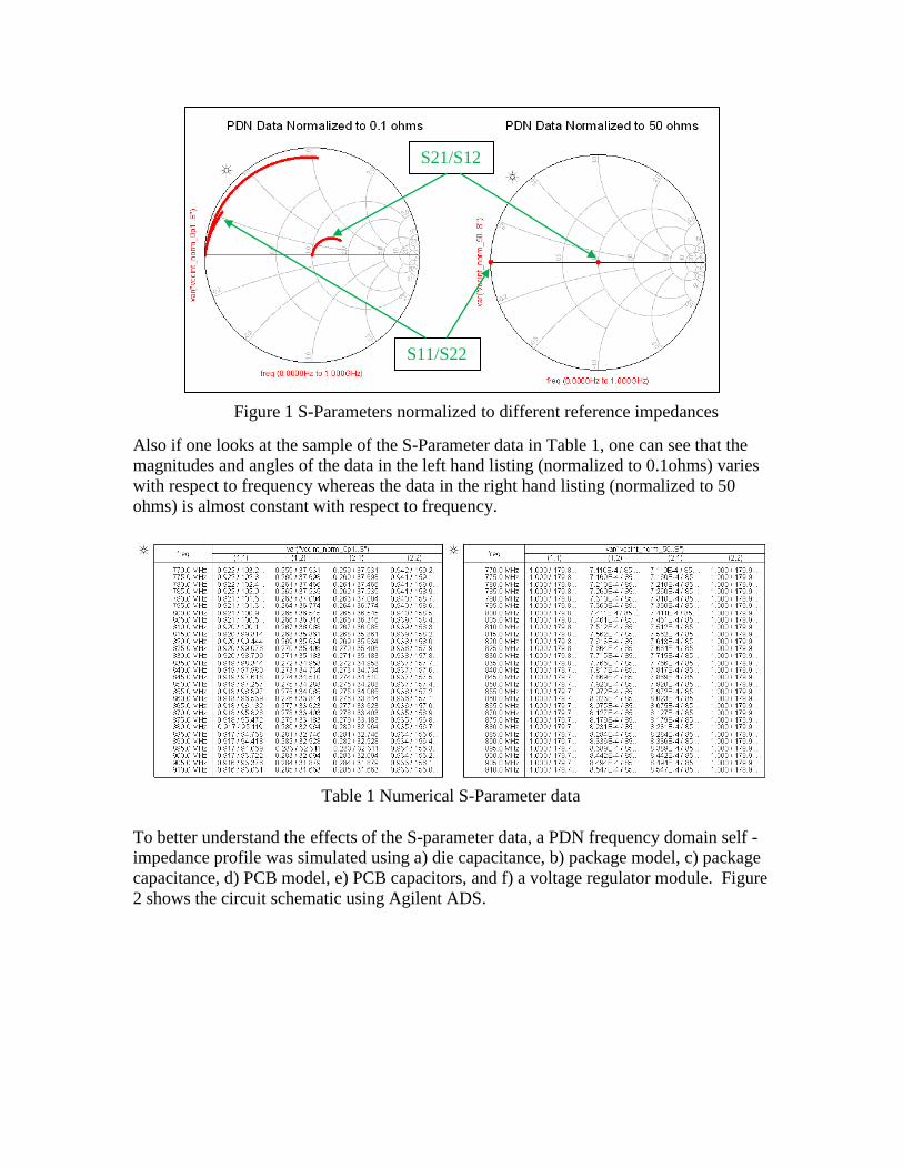
Also if one looks at the sample of the S-Parameter data in Table 1, one can see that the
magnitudes and angles of the data in the left hand listing (normalized to 0.1ohms) varies
with respect to frequency whereas the data in the right hand listing (normalized to 50
ohms) is almost constant with respect to frequency.
To better understand the effects of the S-parameter data, a PDN frequency domain self -
impedance profile was simulated using a) die capacitance, b) package model, c) package
capacitance, d) PCB model, e) PCB capacitors, and f) a voltage regulator module. Figure
2 shows the circuit schematic using Agilent ADS.
Figure 1 S-Parameters normalized to different reference impedances
Table 1 Numerical S-Parameter data
S11/S22
S21/S12

Figure 2 Circuit Schematic of PDN (Power Distribution Network)
The simulation results of the PDN frequency domain self-impedance profile shown in
Figure 3. The plot shows the impedance profile of a PDN where the PDN S-Parameter
data was normalized to 0.1 ohms (plotted in red), along with the simulated response in
the same circuit when the S-Parameter data was normalized to 50 ohms (plotted in blue).
Note the oscillatory nature of the 50 ohm plot as compared to the smooth shape of the
0.1 ohm plot. This illustrates one obvious manifestation of the effects of using data not
normalized properly in a simulation. In some cases the effects may not be so obvious, but
can still distort the simulation results. In time domain simulations, the problems caused
may manifest themselves as non-convergence issues or cause voltage values to blow up
to unrealistic values.
Figure 3 Impedance profile of PDN with different normalization
mO
hm
s
Effected by
Lpackage
Effected by
Cdie
1.2 Model Generation
A so-called SSN S-Parameter model contains two parts: signal trace data and PDN data.
The signal trace S-Parameters are coupled to the PDN as well as to each other. The signal
trace data is typically normalized to 50 ohms while the PDN data is normalized to 0.1
ohms as discussed in the previous section. The S-Parameter model is almost always
generated by means of electromagnetic extraction rather than by measurement since the
models are quite large (a typical model might have 109-ports (106 ports for 52 signal nets
plus 3 ports for the PDN). A model of this complexity is impractical to generate by
measurement. There are several electromagnetic extractors on the market that may be
used to generate these large models. Examples of these extractors include Agilent
Momentum, Cadence PowerSI and Ansys SiWave. These extractors are not full-wave 3D
extractors, but are 2.5D hybrid extractors and are well suited to the job at hand. They are
fully capable of generating the large models required with at least 10 GHz in bandwidth
in a few hours runtime.
The process of generating the SSN model is conceptually quite simple. A CAD design
database is imported into the selected extractor. The stackup dimensions and material
properties are checked and edited as necessary. The dielectric material properties should
be frequency dependent to allow for the generation of causal S-Parameters. Ports are
assigned at both ends of the signal traces as well as at the input, output and decoupling
capacitor connections of the PDN. It is important to make sure the ports associated with
the PDN are normalized to a low impedance around 0.1 ohms. It is necessary to define
the extraction bandwidth. A typical model for SSN use may have a bandwidth of DC to 6
GHz. It is important that the data generated at low frequencies down to DC be accurate
since the model will ultimately be used in a transient simulation. Inaccurate low
frequency data points can lead to convergence issues in transient simulations. An upper
frequency limit in the 6-10 GHz range is usually adequate for SSN simulations. The S-
Parameter output format should be selected to be Touchstone Version 2.0 to allow for the
inclusion of multiple normalization impedances (50 ohms for the signal lines and 0.1
ohms for the PDN). This topic will be discussed further in the following section.
1.3 Touchstone v2.0 models After the SSN model has been extracted using an electromagnetic extractor the resulting
S-Parameter data needs to be utilized in a time domain simulator to perform the actual
SSN simulation. Since there are numerous extractors and numerous simulators that might
be utilized to perform SSN simulations it is convenient that there is a standardized file
format for the S-Parameter data. The current de-facto standard is the Touchstone file
format. The format was developed back in 1984 as the output format for the EEsof
Touchstone simulator. Over the years EEsof was acquired by Agilent and the venerable
Touchstone simulator has long since been superseded by newer, more capable simulators
from Agilent, however the Touchstone file format has survived. A few years ago the
Touchstone version 1.0 format became an EIA standard thanks to work performed by the
IBIS Open Forum. In 2009 a new, enhanced Touchstone version 2.0 format was ratified.
The Touchstone format is a ASCII format where the S-Parameter matrix data is
represented frequency by frequency. A „option line‟ exists at the beginning of the file to
define frequency units, data type, data format and normalization impedance. A typical
version 1.0 header is shown below.
# Hz S RI R 50
In this example, it indicates that the following data frequency units are in Hz, the data is
S-Parameters, the format is Real/Imaginary and that the normalization impedance is 50
ohms. If the frequency unit is not specified it defaults to GHz. The parameter types
supported are: S, Y, Z, H and G. If the parameter type isn‟t specified it defaults to S.
Format parameters are DB (decibel/angle), MA (magnitude/angle) and RI
(real/imaginary). Angles are specified in degrees and Decibel= 20*log10|magnitude|.
An important thing to note is that the Touchstone Version 1.0 format only supports a
single normalization impedance. This means that an SSN model with transmission line
data normalized to 50 ohms and PDN data normalized to 0.1 ohms cannot legally be
represented in a Touchstone Version 1.0 file. Hspice supports a proprietary enhancement
that allows users to specify multiple normalization impedances. An example would be:
# Hz S RI R 50 50 50 0.1
Version 1.0 models using the proprietary format are only generated by Cadence PowerSI.
This option line would only be properly parsed and acted on in the Hspice simulator.
Other simulators would either fail to parse the file or may generate indeterminate results.
Touchstone Version 2.0 solves this problem and officially allows for the support of
multiple normalization impedances. More on Version 2.0 in a moment, but what can one
do if they need to run a SSN simulation in a simulator that doesn‟t support the proprietary
Hspice enhancement or Touchstone Version 2.0? In the simulation environment, perfect
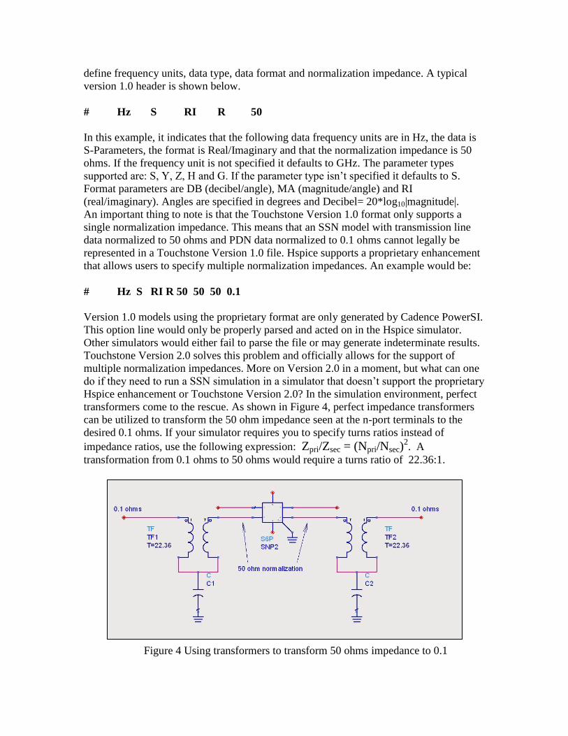
transformers come to the rescue. As shown in Figure 4, perfect impedance transformers
can be utilized to transform the 50 ohm impedance seen at the n-port terminals to the
desired 0.1 ohms. If your simulator requires you to specify turns ratios instead of
impedance ratios, use the following expression: Zpri/Zsec = (Npri/Nsec)2. A
transformation from 0.1 ohms to 50 ohms would require a turns ratio of 22.36:1.
Figure 4 Using transformers to transform 50 ohms impedance to 0.1
ohms
The capacitors shown connected to the bottoms of each transformer serve to provide a
very low AC impedance to ground and at the same time not cause any DC current flow
issues. The value for the capacitor needs to be large enough to present a very low
impedance a very low frequencies.
While the perfect transformer scheme does work, it isn‟t very elegant. The real answer to
this dilemma of how to support multiple normalization impedances is the use of
Touchstone Version 2.0 models. Version 2.0 supports a lot of enhancements over the
older Version 1.0 models, but the most important one for the SSN simulation work is the
support of multiple normalization impedances. Touchstone Version 2.0 is now supported
by most current generation extractors and simulators. Extractors such as Agilent
Momentum , Cadence PowerSI, , and Ansys SIwave and HFSS support the generation of
Touchstone Version 2.0 data files. On the Transient simulator side, Touchstone Version
2.0 S-Parameter files may be read by Agilent Advanced Design System, Ansys Designer
and Synopsys Hspice and others.
The Touchstone Version 2.0 specification document may be downloaded at the following
URL: http://www.vhdl.org/ibis/touchstone_ver2.0/touchstone_ver2_0.pdf.
The following is an example of a simple 4-port Version 2.0 header and option line:
[Version] 2.0
# GHz S MA R 50
[Number of Ports] 4
[Reference]
50 50 0.01 0.01
[Number of Frequencies] 50
The [Version] keyword is required. The option line is quite similar to the one in Version
1.0 files. It is required to define the number of ports in the model by use of the [Number
of Ports] keyword. The important part for our SSN simulation purposes is the [Reference]
keyword. In this example it defines ports 1 and 2 as being normalized to 50 ohms and
ports 3 and 4 as being normalized to 0.1 ohms. It is also necessary to define the number
of frequencies modeled by the data. It is highly recommended that the above referenced
specification document be downloaded and utilized to understand all the options and
capabilities available in Touchstone 2.0 models.
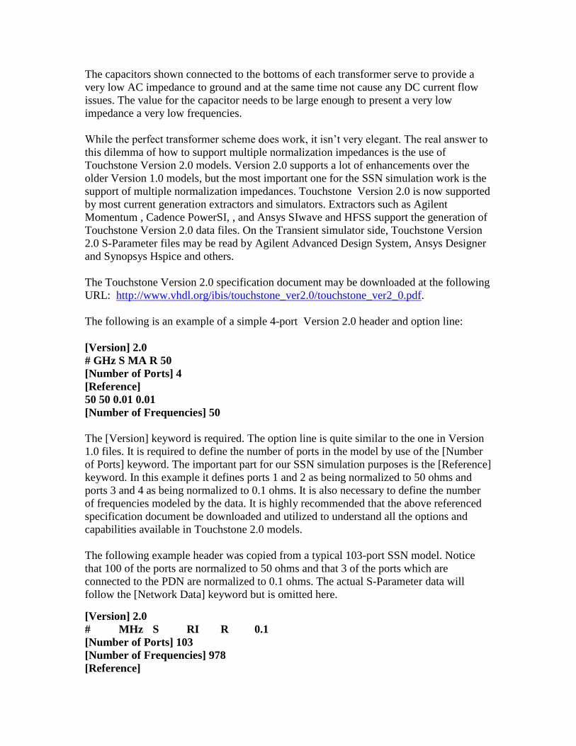
The following example header was copied from a typical 103-port SSN model. Notice
that 100 of the ports are normalized to 50 ohms and that 3 of the ports which are
connected to the PDN are normalized to 0.1 ohms. The actual S-Parameter data will
follow the [Network Data] keyword but is omitted here.
[Version] 2.0
# MHz S RI R 0.1
[Number of Ports] 103
[Number of Frequencies] 978
[Reference]
0.1 50 50 50 50 50 50 50 50 50 50 50 50 50 50 50 50 50 50 50 50 50 50 50 50 50 50 50
50 50 50 50 50 50 50 50 50 50 50 50 50 50 50 50 50 50 50 50 50 50 50 0.1 50 50 50 50
50 50 50 50 50 50 50 50 50 50 50 50 50 50 50 50 50 50 50 50 50 50 50 50 50 50 50 50 50
50 50 50 50 50 50 50 50 50 50 50 50 50 50 50 50 50 0.1
[Network Data]
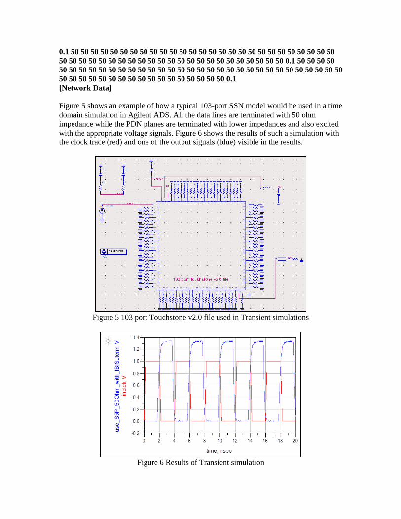
Figure 5 shows an example of how a typical 103-port SSN model would be used in a time
domain simulation in Agilent ADS. All the data lines are terminated with 50 ohm
impedance while the PDN planes are terminated with lower impedances and also excited
with the appropriate voltage signals. Figure 6 shows the results of such a simulation with
the clock trace (red) and one of the output signals (blue) visible in the results.
Figure 5 103 port Touchstone v2.0 file used in Transient simulations
Figure 6 Results of Transient simulation

2. IBIS v5.0 models
To accurately simulate SSN requires IO models for the memory controller and the
DRAM devices. Traditionally, transistor level Hspice netlists have been used to model
the IOs. However, high accuracy simulations required post layout transistor netlist
transistor netlists which require significant CPU and RAM resources. To resolve these
issues, the IBIS committee introduced power-aware IBIS v5.0 models.
In August 2008, the IBIS open forum committee ratified IBIS v5.0. There are two BIRDs
related to the power awareness of the IBIS v5.0 models. Additionally, there is one BIRD
ratified as part of IBIS v4.2 which is equally important to achieving accurate SSN
simulations.
The first power aware BIRD is 95.6. The title of BIRD 95.6 is “Power Integrity Analysis
using IBIS”. This BIRD introduces the keyword [Composite Current]. The [Composite
Current] keyword describes the waveform shape of the rising and falling edge currents
originating from the power supply terminal of the buffer. The data contained in the *.ibs
file consists of a table of power supply current vs. time (I-T). These (I-T) tables use the
same test fixture load conditions as the (V-T) data associated with the keywords [rising
waveform] and [falling waveform].
The second power aware BIRD is 98.3. The title of BIRD 98.3 is “Gate Modulation
Effect”. BIRD 98.3 adds to the *.ibs file two new keywords [ISSO PU] and [ISSO PD].
These keywords provide tables of the effective saturation current with respect to the
voltage variation of the reference supplies.
Thirdly, BIRD 76.1 was ratified as part of IBIS v4.2. The title of BIRD 76.1 is
“Additional Information Related to C_comp Refinements”. IBIS models can have up to
four I-V tables, each of which can have their own supply connection (node). BIRD 76.1
seeks to allow a unique C_comp value for each of these four I-V curves. These four
C_comp values allow the splitting of the total pad capacitance between each of these
supply nodes. This can be important for power integrity simulations to couple the signal
on the IO pad to the appropriate supply node. C_comp_pullup is in parallel with the PU I-
V curve. C_comp_power_clamp is in parallel with the PC I-V curve. C_comp_pulldown
is in parallel with the PD I-V curve. C_comp_gnd_clamp is in parallel with the GC I-V
curve. The individual 4 I-V curves can be separately turned on/off by switching the
buffer to low/high/tri-state. However, the C_comp_* are always on.
3. DDR4
3.1 PDN Noise
DDR4 system level design is complex and challenging and contains significant
architectural changes as compared to DDR3 architecture. Regarding SI/PI (Signal
Integrity/Power Integrity) system level design, there are two key architectural changes
which can be summarized as follows:
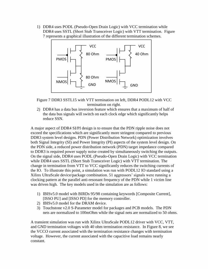
1) DDR4 uses PODL (Pseudo-Open Drain Logic) with VCC termination while
DDR4 uses SSTL (Short Stub Transceiver Logic) with VTT termination. Figure
7 represents a graphical illustration of the different termination schemes.
Figure 7 DDR3 SSTL15 with VTT termination on left, DDR4 PODL12 with VCC
termination on right.
2) DDR4 has a data bus inversion feature which ensures that a maximum of half of
the data bus signals will switch on each clock edge which significantly helps
reduce SSN.
A major aspect of DDR4 SI/PI design is to ensure that the PDN ripple noise does not
exceed the specifications which are significantly more stringent compared to previous
DDR3 system level designs. PDN (Power Distribution Network) optimization involves
both Signal Integrity (SI) and Power Integrity (PI) aspects of the system level design. On
the PDN side, a reduced power distribution network (PDN) target impedance compared
to DDR3 is required power supply noise created by simultaneously switching the outputs.
On the signal side, DDR4 uses PODL (Pseudo-Open Drain Logic) with VCC termination
while DDR4 uses SSTL (Short Stub Transceiver Logic) with VTT termination. The
change in termination from VTT to VCC significantly reduces the switching currents of
the IO. To illustrate this point, a simulation was run with PODL12 IO standard using a
Xilinx UltraScale device/package combination. 51 aggressors‟ signals were running a
clocking pattern at the parallel anti-resonant frequency of the PDN while 1 victim line
was driven high. The key models used in the simulation are as follows:
1) IBISv5.0 model with BIRDs 95/98 containing keywords [Composite Current],
[ISSO PU] and [ISSO PD] for the memory controller.
2) IBISv5.0 model for the DRAM device.
3) Touchstone v2.0 S-Parameter model for packages and PCB models. The PDN
nets are normalized to 100mOhm while the signal nets are normalized to 50 ohms.
A transient simulation was run with Xilinx UltraScale PODL12 driver with VCC, VTT,
and GND termination voltages with 40 ohm termination resistance. In Figure 8, we see
the VCCO current associated with the termination resistance changes with termination
voltage. However, the current associated with the capacitive load remains nearly
constant.
PMOS PMOS
NMOS NMOS
VCC
80 Ohm
80 Ohm
GND
40 Ohm
VCC
GND
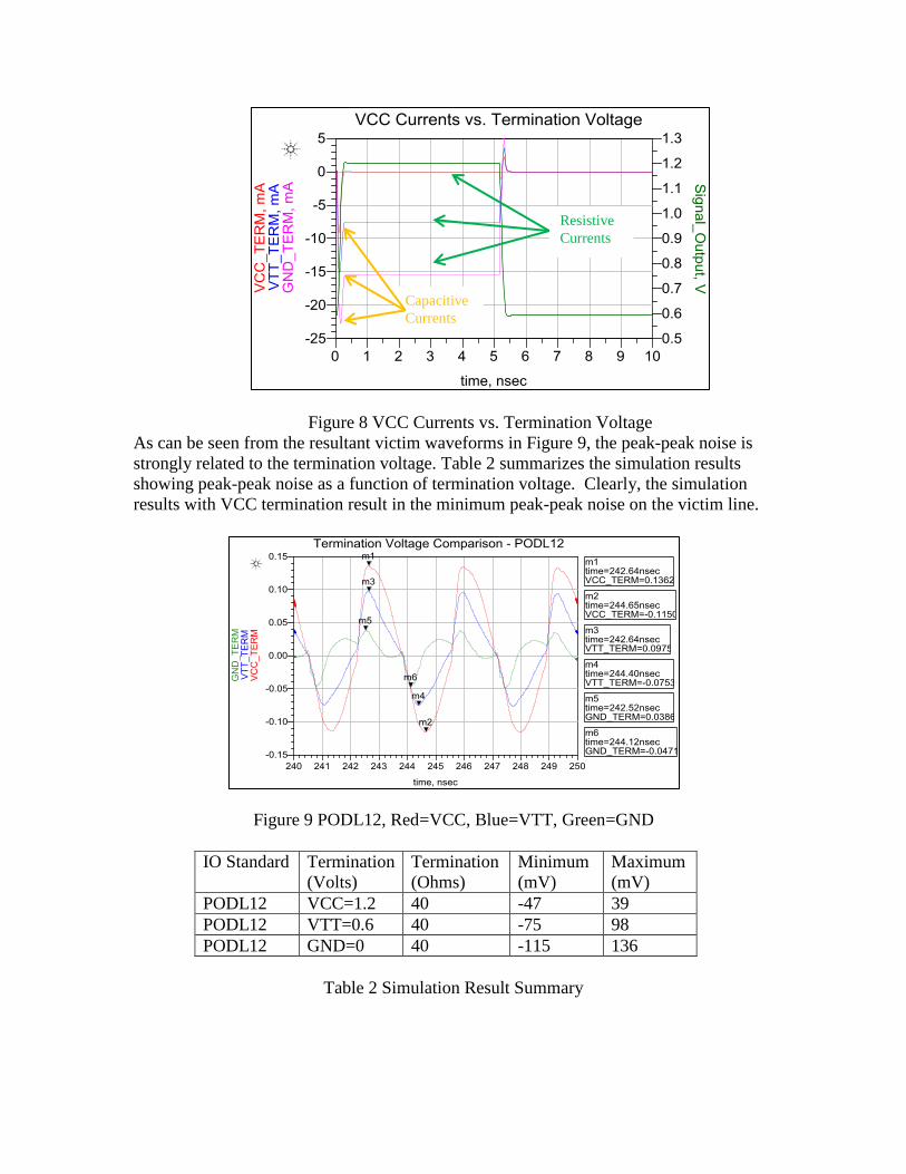
Figure 8 VCC Currents vs. Termination Voltage
As can be seen from the resultant victim waveforms in Figure 9, the peak-peak noise is
strongly related to the termination voltage. Table 2 summarizes the simulation results
showing peak-peak noise as a function of termination voltage. Clearly, the simulation
results with VCC termination result in the minimum peak-peak noise on the victim line.
Figure 9 PODL12, Red=VCC, Blue=VTT, Green=GND
IO Standard Termination
(Volts)
Termination
(Ohms)
Minimum
(mV)
Maximum
(mV)
PODL12 VCC=1.2 40 -47 39
PODL12 VTT=0.6 40 -75 98
PODL12 GND=0 40 -115 136
Table 2 Simulation Result Summary
Resistive
Currents
Capacitive
Currents
3.2 Minimizing Crosstalk
To meet the stringent timing requirements of DDR4, crosstalk should be minimized. To
simulate crosstalk, Touchstone v2.0 models should be used including both power nets
and signal nets. Touchstone v2.0 allows crosstalk to be simulated from any net to any
other net including 1) signal nets to signal nets as well as 2) signal nets to power nets and
3) power nets to signal nets. In a homogenous dielectric, crosstalk is theoretically reverse
prorogating only (NEXT). However, most dielectric materials have a small component
of forward propagating crosstalk (FEXT) due to the fact that most dielectrics are not
entirely homogenous. Because most crosstalk is NEXT, great care should be taken to
match the Rout of the PODL Driver to the transmission line interconnect to reduce the
crosstalk noise contribution to the total noise budget. Both mutual capacitance Cm
(electric field) and mutual inductance Lm (magnetic field) exist between victim and
aggressor lines. The mutual inductance will induce current on the victim line opposite of
the aggressor line (Lens‟s Law). The mutual capacitance will pass current through the
mutual capacitance that flows in both directions on the victim line. The near and far end
victim line currents sum to produce the NEXT and FEXT components. I(Next) = I(Cm)
+ I(Lm) while I(Fext) = I(Cm) – I(Lm). NEXT is always positive. FEXT for
homogenous dielectrics is theoretically zero for stripline transmission lines because the
speed of propagation for odd and even modes of propagation are equal. Thus, to reduce
crosstalk noise, the focus should be on NEXT as opposed to FEXT.
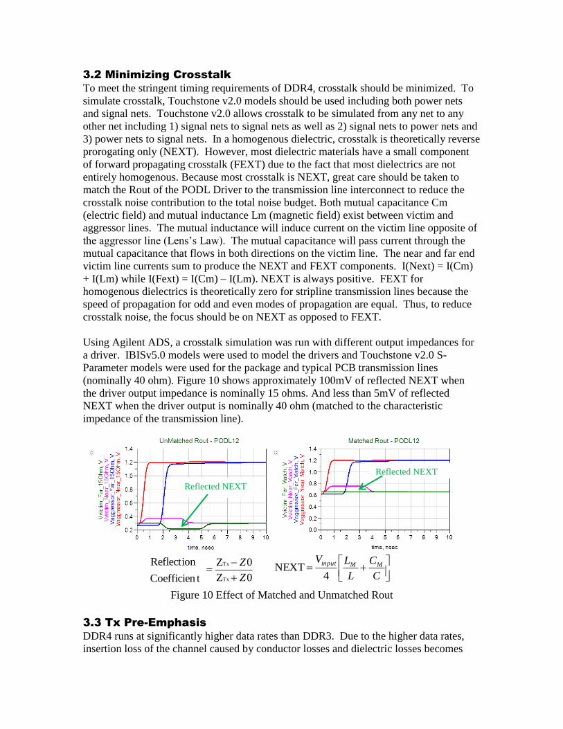
Using Agilent ADS, a crosstalk simulation was run with different output impedances for
a driver. IBISv5.0 models were used to model the drivers and Touchstone v2.0 S-
Parameter models were used for the package and typical PCB transmission lines
(nominally 40 ohm). Figure 10 shows approximately 100mV of reflected NEXT when
the driver output impedance is nominally 15 ohms. And less than 5mV of reflected
NEXT when the driver output is nominally 40 ohm (matched to the characteristic
impedance of the transmission line).
Figure 10 Effect of Matched and Unmatched Rout
3.3 Tx Pre-Emphasis
DDR4 runs at significantly higher data rates than DDR3. Due to the higher data rates,
insertion loss of the channel caused by conductor losses and dielectric losses becomes
C
C
L
LVMMinput
4NEXT
0Z
0Z
Tx
Tx
Z
Z
tCoefficien
Reflection
Reflected NEXT
Reflected NEXT
significant as compared to DDR3. To compensate for channel insertion loss during a
write operation, the memory controller's driver architecture may require pre-emphasis.
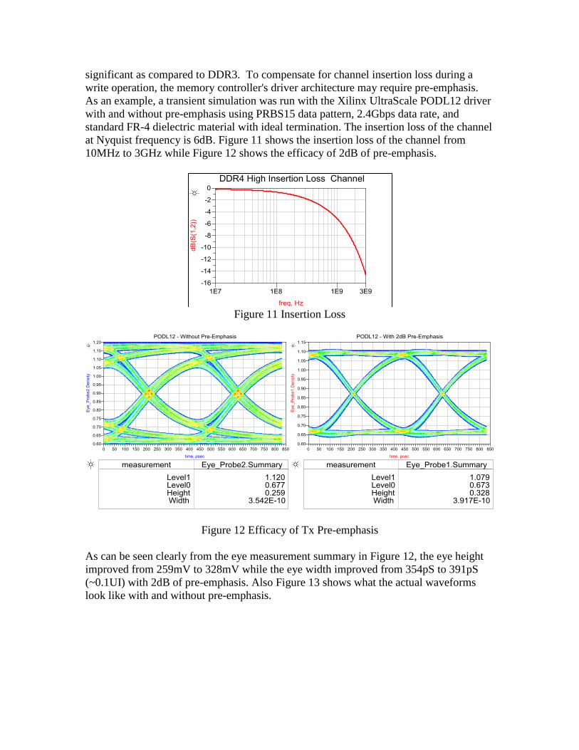
As an example, a transient simulation was run with the Xilinx UltraScale PODL12 driver
with and without pre-emphasis using PRBS15 data pattern, 2.4Gbps data rate, and
standard FR-4 dielectric material with ideal termination. The insertion loss of the channel
at Nyquist frequency is 6dB. Figure 11 shows the insertion loss of the channel from
10MHz to 3GHz while Figure 12 shows the efficacy of 2dB of pre-emphasis.
Figure 11 Insertion Loss
Figure 12 Efficacy of Tx Pre-emphasis
As can be seen clearly from the eye measurement summary in Figure 12, the eye height
improved from 259mV to 328mV while the eye width improved from 354pS to 391pS
(~0.1UI) with 2dB of pre-emphasis. Also Figure 13 shows what the actual waveforms
look like with and without pre-emphasis.
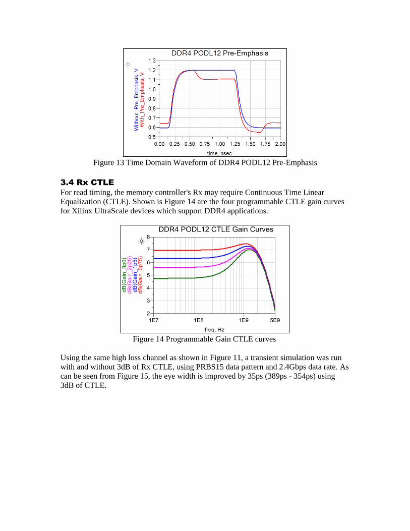
Figure 13 Time Domain Waveform of DDR4 PODL12 Pre-Emphasis
3.4 Rx CTLE
For read timing, the memory controller's Rx may require Continuous Time Linear
Equalization (CTLE). Shown is Figure 14 are the four programmable CTLE gain curves
for Xilinx UltraScale devices which support DDR4 applications.
Figure 14 Programmable Gain CTLE curves
Using the same high loss channel as shown in Figure 11, a transient simulation was run
with and without 3dB of Rx CTLE, using PRBS15 data pattern and 2.4Gbps data rate. As
can be seen from Figure 15, the eye width is improved by 35ps (389ps - 354ps) using
3dB of CTLE.
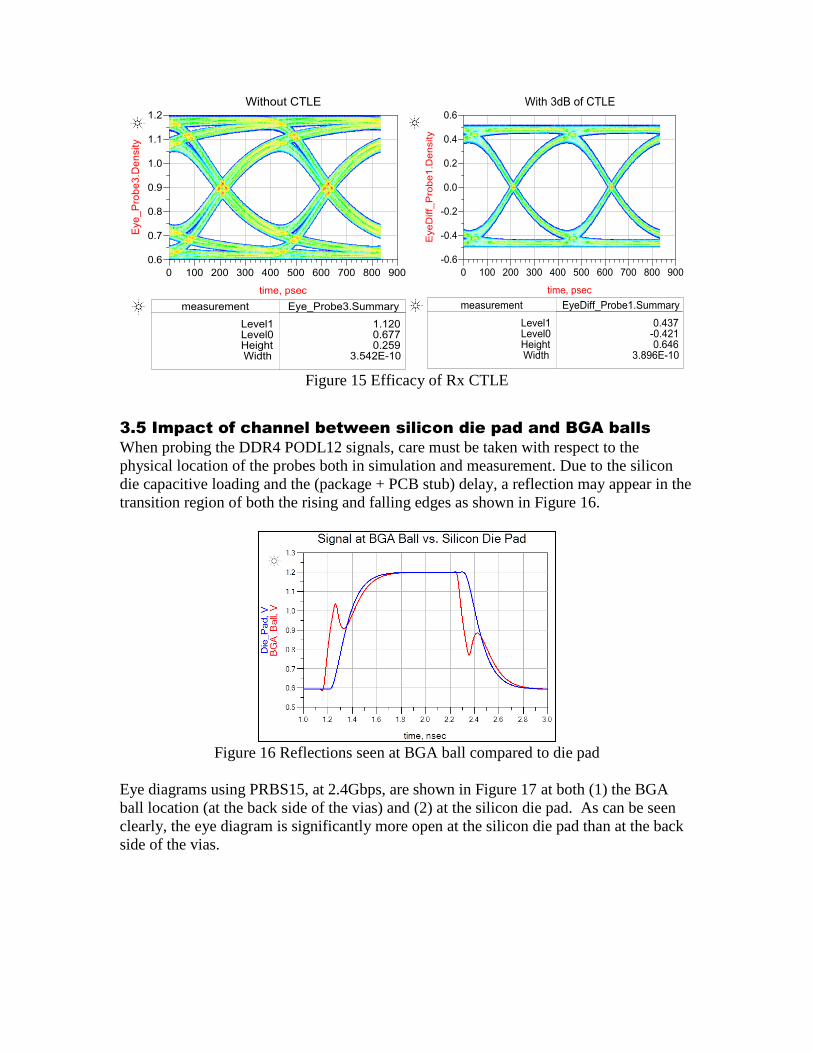
Figure 15 Efficacy of Rx CTLE
3.5 Impact of channel between silicon die pad and BGA balls
When probing the DDR4 PODL12 signals, care must be taken with respect to the
physical location of the probes both in simulation and measurement. Due to the silicon
die capacitive loading and the (package + PCB stub) delay, a reflection may appear in the
transition region of both the rising and falling edges as shown in Figure 16.
Figure 16 Reflections seen at BGA ball compared to die pad
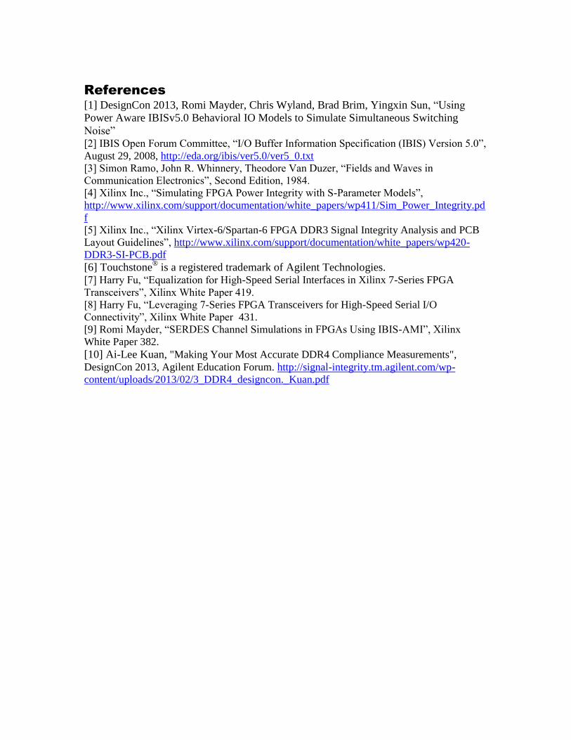
Eye diagrams using PRBS15, at 2.4Gbps, are shown in Figure 17 at both (1) the BGA
ball location (at the back side of the vias) and (2) at the silicon die pad. As can be seen
clearly, the eye diagram is significantly more open at the silicon die pad than at the back
side of the vias.
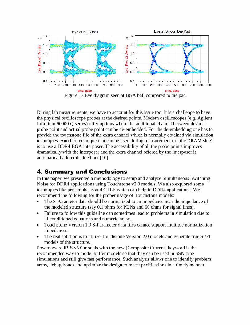
Figure 17 Eye diagram seen at BGA ball compared to die pad
During lab measurements, we have to account for this issue too. It is a challenge to have
the physical oscilloscope probes at the desired points. Modern oscilloscopes (e.g. Agilent
Infiniium 90000 Q series) offer options where the additional channel between desired
probe point and actual probe point can be de-embedded. For the de-embedding one has to
provide the touchstone file of the extra channel which is normally obtained via simulation
techniques. Another technique that can be used during measurement (on the DRAM side)
is to use a DDR4 BGA interposer. The accessibility of all the probe points improves
dramatically with the interposer and the extra channel offered by the interposer is
automatically de-embedded out [10].
4. Summary and Conclusions
In this paper, we presented a methodology to setup and analyze Simultaneous Switching
Noise for DDR4 applications using Touchstone v2.0 models. We also explored some
techniques like pre-emphasis and CTLE which can help in DDR4 applications. We
recommend the following for the proper usage of Touchstone models:
The S-Parameter data should be normalized to an impedance near the impedance of
the modeled structure (say 0.1 ohms for PDNs and 50 ohms for signal lines).
Failure to follow this guideline can sometimes lead to problems in simulation due to
ill conditioned equations and numeric noise.
Touchstone Version 1.0 S-Parameter data files cannot support multiple normalization
impedances.
The real solution is to utilize Touchstone Version 2.0 models and generate true SI/PI
models of the structure.
Power aware IBIS v5.0 models with the new [Composite Current] keyword is the
recommended way to model buffer models so that they can be used in SSN type
simulations and still give fast performance. Such analysis allows one to identify problem
areas, debug issues and optimize the design to meet specifications in a timely manner.
References
[1] DesignCon 2013, Romi Mayder, Chris Wyland, Brad Brim, Yingxin Sun, “Using
Power Aware IBISv5.0 Behavioral IO Models to Simulate Simultaneous Switching
Noise” [2] IBIS Open Forum Committee, “I/O Buffer Information Specification (IBIS) Version 5.0”,
August 29, 2008, http://eda.org/ibis/ver5.0/ver5_0.txt
[3] Simon Ramo, John R. Whinnery, Theodore Van Duzer, “Fields and Waves in
Communication Electronics”, Second Edition, 1984.
[4] Xilinx Inc., “Simulating FPGA Power Integrity with S-Parameter Models”,
http://www.xilinx.com/support/documentation/white_papers/wp411/Sim_Power_Integrity.pd
f
[5] Xilinx Inc., “Xilinx Virtex-6/Spartan-6 FPGA DDR3 Signal Integrity Analysis and PCB
Layout Guidelines”, http://www.xilinx.com/support/documentation/white_papers/wp420-
DDR3-SI-PCB.pdf
[6] Touchstone® is a registered trademark of Agilent Technologies.
[7] Harry Fu, “Equalization for High-Speed Serial Interfaces in Xilinx 7-Series FPGA
Transceivers”, Xilinx White Paper 419. [8] Harry Fu, “Leveraging 7-Series FPGA Transceivers for High-Speed Serial I/O
Connectivity”, Xilinx White Paper 431. [9] Romi Mayder, “SERDES Channel Simulations in FPGAs Using IBIS-AMI”, Xilinx
White Paper 382.
[10] Ai-Lee Kuan, "Making Your Most Accurate DDR4 Compliance Measurements",
DesignCon 2013, Agilent Education Forum. http://signal-integrity.tm.agilent.com/wp-
content/uploads/2013/02/3_DDR4_designcon._Kuan.pdf