Design techniques for high-speed, high-resolution ... · PDF fileDesign Techniques for...
11
1916 IEEE JOURNAL OF SOLID-STATE CIRCUITS. VOL. 27. NO. 12. DECEMBER 1992 Design Techniques for High-speed, High-Resolution Comparators Behzad Razavi, Member, IEEE, and Bruce A. Wooley, Fellow, IEEE Abstract-This paper describes precision techniques for the design of comparatorsused in high-performance analog-to-dig- ita1 convertersemploying parallel conversion stages. Following a review of conventional offset cancellation techniques, circuit designs achieving 12-b resolution in both BiCMOS and CMOS 5-V technologiesare presented. The BiCMOS comparator con- sists of a preamplifier followed by two regenerative stages and achieves an offset of 200 pV at a IO-MHz clock rate while dis- sipating 1.7 mW. In the CMOS comparator offset cancellation is used in both a single-stage preamplifier and a subsequent latch to achieve an offset of less than 300 pV at comparison rates as high as 10 MHz, with a power dissipation of 1.8 mW. I. INTRODUCTION The next section of this paper reviews some of the con- ventional approaches to offset cancellation and identifies their fundamental trade-offs and limitations. The Bi- CMOS comparator is then described in Section 111, and the design of the CMOS comparator is presented in Sec- tion IV. The experimental results obtained for both cir- cuits are summarized in Section V. 11. OFFSET CANCELLATION TECHNIQUES A. Circuit Topologies The analog sampling capability inherent in CMOS and BiCMOS technologies provides a means whereby offsets N high-speed analog-to-digital converters, comparator can be Periodical'Y sensed, stored, and then subtracted Idesign has a crucial influence on the overall perfor- from the input incorporate a large number of comparators in parallel to Offset (Ios) and Output Offset ('Os), on the delay, resolution, power dissipation, input voltage two approaches as to a 'Ompar- range, input impedance, and area of those circuits. More- comprises a preamplifier, Of the various Offset mance that can be achieved. Converter architectures that two Of the most ' ' " On approaches' based On obtain a high throughput rate impose stringent constraints are considered herein. Fig. l(a> and (b) illustrates these ator* Each Of these over, the relatively large device mismatch and limited offset storage capacitors, and a latch. With IOS, the can- voltage range that accompany the integration of compar- cellation is Performed a unitY-gain loop around ator circuits in low-voltage scaled VLSI technologies se- verely compromise the precision that can be obtained. This paper introduces a number of comparator design techniques for use in parallel A/D converters that are im- the preamplifier and storing the Offset On the input piing capacitors. With Oos? the Offset is by shorting the preamplifier inputs and storing the amp1ified Offset On the Output Of capacitors* A plemented in BiCMOS and CMOS vLsI technologies. The suggested methods are intended to provide improved resolution and speed while maintaining low power dissi- pation, a small input capacitance, and low complexity. The techniques are presented within the context of prac- these two approaches reveals their respective merits and In the comparator with IOS, the residual input-referred Offset (i.e.7 the Offset after is (1) vosi AQ VOX. v,, = ___ +-+- tical designs for both a BiCMOS and a CMOS comparator BiCMOS comparator employs a low-gain Preamplifier followed by two regenerative amplifiers to achieve an off- set Of 200 pv at 'lock as high as lo MHz. In the CMOS comparator, ofiset cancellation is used in both the preamplifier and the subsequent latch to achieve an offset of less than 300 pV at 10 MHz. with 12-b resolution at 10-MHz comparison rates. The 1 + A0 C A0 where v,,, and A. are the input offset and gain of the preamplifier, respectively, AQ is the mismatch in charge injection from switches S5 and S6 onto capacitors C 1 and c2, and v, is the latch offset. In the comparator em- ploying oos, the residual offset is (2) AQ vox v,, = - + -. AoC A0 Manuscript received March 4, 1992; revised July 13, 1992. This work was supported by the Army Research Office under Contract DAAL03-91- G-0088. B. Razavi was with the Center for Integrated Systems, Stanford Univer- Equations ( l ) and (2) show that, for similar preamplifiers, sity, Stanford, CA 94305. He is now with AT&T Bell Laboratories, Holm- del, NJ 07733. B. A. Wooley is with the Center for Integrated Systems, Stanford Uni- versitv. Stanford. CA 94305. the residual offset obtainable using 00s can be Smaller than that for 10s. In fact, unless sufficient statistical data for V,, AQ, and VosL are available, 10s requires the use ~~ IEEE Log Number 9204 135. of quite large values for A. and C to guarantee a low Vas. 0018-9200/92$03.00 0 1992 IEEE
Transcript of Design techniques for high-speed, high-resolution ... · PDF fileDesign Techniques for...

1916 IEEE JOURNAL OF SOLID-STATE CIRCUITS. VOL. 27. NO. 12. DECEMBER 1992
Design Techniques for High-speed, High-Resolution Comparators
Behzad Razavi, Member, IEEE, and Bruce A. Wooley, Fellow, IEEE
Abstract-This paper describes precision techniques for the design of comparators used in high-performance analog-to-dig- ita1 converters employing parallel conversion stages. Following a review of conventional offset cancellation techniques, circuit designs achieving 12-b resolution in both BiCMOS and CMOS 5-V technologies are presented. The BiCMOS comparator con- sists of a preamplifier followed by two regenerative stages and achieves an offset of 200 pV at a IO-MHz clock rate while dis- sipating 1.7 mW. In the CMOS comparator offset cancellation is used in both a single-stage preamplifier and a subsequent latch to achieve an offset of less than 300 pV at comparison rates as high as 10 MHz, with a power dissipation of 1.8 mW.
I. INTRODUCTION
The next section of this paper reviews some of the con- ventional approaches to offset cancellation and identifies their fundamental trade-offs and limitations. The Bi- CMOS comparator is then described in Section 111, and the design of the CMOS comparator is presented in Sec- tion IV. The experimental results obtained for both cir- cuits are summarized in Section V.
11. OFFSET CANCELLATION TECHNIQUES A. Circuit Topologies
The analog sampling capability inherent in CMOS and BiCMOS technologies provides a means whereby offsets
N high-speed analog-to-digital converters, comparator can be Periodical'Y sensed, stored, and then subtracted Ides ign has a crucial influence on the overall perfor- from the input
incorporate a large number of comparators in parallel to Offset (Ios) and Output Offset ('Os),
on the delay, resolution, power dissipation, input voltage two approaches as to a 'Ompar- range, input impedance, and area of those circuits. More- comprises a preamplifier,
Of the various Offset
mance that can be achieved. Converter architectures that two Of the most ''"On approaches' based On
obtain a high throughput rate impose stringent constraints are considered herein. Fig. l(a> and (b) illustrates these
ator* Each Of these over, the relatively large device mismatch and limited offset storage capacitors, and a latch. With IOS, the can- voltage range that accompany the integration of compar- cellation is Performed a unitY-gain loop around ator circuits in low-voltage scaled VLSI technologies se- verely compromise the precision that can be obtained.
This paper introduces a number of comparator design techniques for use in parallel A/D converters that are im-
the preamplifier and storing the Offset On the input piing capacitors. With Oos? the Offset is by shorting the preamplifier inputs and storing the amp1ified Offset On the Output Of capacitors* A
plemented in BiCMOS and CMOS vLsI technologies. The suggested methods are intended to provide improved resolution and speed while maintaining low power dissi- pation, a small input capacitance, and low complexity. The techniques are presented within the context of prac-
these two approaches reveals their respective merits and
In the comparator with IOS, the residual input-referred Offset (i.e.7 the Offset after is
(1) vosi AQ VOX. v,, = ___ + - + - tical designs for both a BiCMOS and a CMOS comparator
BiCMOS comparator employs a low-gain Preamplifier followed by two regenerative amplifiers to achieve an off- set Of 200 pv at 'lock as high as lo MHz. In the CMOS comparator, ofiset cancellation is used in both the preamplifier and the subsequent latch to achieve an offset of less than 300 pV at 10 MHz.
with 12-b resolution at 10-MHz comparison rates. The 1 + A0 C A0
where v,,, and A. are the input offset and gain of the preamplifier, respectively, AQ is the mismatch in charge injection from switches S5 and S6 onto capacitors C 1 and c 2 , and v,, is the latch offset. In the comparator em- ploying oos, the residual offset is
(2) AQ vox v,, = - + -. AoC A0 Manuscript received March 4 , 1992; revised July 13, 1992. This work
was supported by the Army Research Office under Contract DAAL03-91- G-0088.
B. Razavi was with the Center for Integrated Systems, Stanford Univer- Equations ( l ) and (2) show that, for similar preamplifiers, sity, Stanford, CA 94305. He is now with AT&T Bell Laboratories, Holm- del, NJ 07733.
B. A. Wooley is with the Center for Integrated Systems, Stanford Uni- versitv. Stanford. CA 94305.
the residual offset obtainable using 00s can be Smaller than that for 10s. In fact, unless sufficient statistical data for V,, AQ, and VosL are available, 10s requires the use
~~
IEEE Log Number 9204 135. of quite large values for A. and C to guarantee a low Vas.
0018-9200/92$03.00 0 1992 IEEE

RAZAVI AND WOOLEY: DESIGN TECHNIQUES FOR HIGH-SPEED, HIGH-RESOLUTION COMPARATORS 1917
vi,
(b) Fig. 1 . Comparator offset cancellation techniques: (a) input offset storage,
and (b) output offset storage.
Since the value of the input coupling capacitors with 10s is governed by charge injection, k T / C noise, and at- tenuation considerations, the input capacitance of this to- pology is usually higher than that of the 00s configura- tion. During offset cancellation, the input capacitance of the 10s circuit is equal to the offset storage capacitor, while in the comparison mode it is approximately the sum of the input capacitance of the preamplifier and the para- sitic capacitances of the offset storage capacitor. These parasitic capacitances are typically as large as 0.1 to 0 . 2 pF for input storage capacitors in the range of 0.5 to 1 pF, whereas the preamplifier input capacitance can be maintained below 30 fF. For this reason 00s is generally preferable in flash stages, where many comparators are connected in parallel. Of course, the dc coupling at the input of an 00s comparator limits the common-mode range. Also, in applications where a large differential ref- erence voltage must be stored in the comparator [ 2 ] , the preamplifier of the 00s topology must be designed for a low gain so that it does not saturate at its output.
While 10s is accomplished by means of a closed feed- back loop, which forces the preamplifier into its active region, 00s is normally an open-loop operation that re- quires tight control of the amplifier gain. Therefore, 00s is typically implemented using a single-stage amplifier with a gain of less than 10 to ensure operation in the active region under extreme variations in device matching and supply voltage.
In conventional CMOS comparator designs, the pream- plifier is typically followed by a standard dynamic CMOS latch. As shown in the following subsection, this latch has a potentially large input offset and therefore requires the use of a high-gain preamplifier in order to achieve a low offset. Consequently, in high-resolution applications a single stage of 00s cannot be used, while a single-stage high-gain preamplifier with 10s suffers from a long delay.
The above considerations have led to the use of multi- stage calibration techniques in high-resolution applica-
T
Fig. 2. Multistage offset cancellation
tions. Fig. 2 illustrates a typical multistage comparator topology that, in effect, utilizes both 10s and 00s when it is clocked sequentially [2], [ 3 ] . The overall gain of the circuit is chosen so that an input of 0.5 LSB overcomes the offset of the latch (50 to 100 mV), and the number of stages is then selected to provide the smallest delay [ 2 ] .
In the configuration of Fig. 2 a large latch offset is ac- commodated through the use of multiple preamplifier stages, each with offset cancellation. Alternatively, the offset of the latch can be reduced so as to relax the gain required of the preamplifier. This can be accomplished through the use of either devices with inherently low off- sets or offset cancellation in the latch.
B. Design Constraints in a Dynamic CMOS h t c h In order to synchronize the operation of a comparator
with other parts of a system, as well as provide the gain needed to generate logic levels at the output, a regenera- tive amplifier is normally used as the final comparator stage. Fig. 3 shows a dynamic CMOS latch similar to that used in [4] to amplify small differences to CMOS levels. In this circuit, when 9 is low, M5 is off, SI and S 2 are on, and the latch senses the inputs Vjnl and Vjn2. When 9 goes high, S1 and S2 turn off to isolate nodes X and Y from input terminals and M5 turns on to initiate regen- eration.
In order to simplify calculations and estimate a lower bound for the offset of the latch in Fig. 3 , only the mis- matches between M 1 and M 2 and between S 1 and S 2 are considered here. In practice, other errors such as mis- matches between M 3 and M 4 further increase the offset. Considering only the M1, M2 and S1, S 2 mismatches, the input offset of the latch can be expressed as
( 3 )
where AV,, and V,, are the standard deviation and mean of the threshold voltage, A W / W and U / L are relative dimension mismatches, VGs - VTH represents the initial gate-source overdrive, AQ is the charge injection mis- match between S 1 and S2, and CD is the total capacitance at X or Y (assumed equal on both sides). For optimistic values of AVTH = 5 mV, A W / W = A L / L = 0.05, VGs - VTH = 1 V, AQ = 0.5 fC, and CD = 100 fF, the latch offset voltage is approximately 60 mV, with its major component arising from the second term in ( 3 ) . This term can be reduced by increasing W and L and/or decreasing VGs - VTH, i.e., decreasing the initial drain current of M 1 and M 2 . However, these remedies can degrade the speed
1918 IEEE JOURNAL OF SOLID-STATE CIRCUITS, VOL. 27. NO. 12. DECEMBER 1992
I I -
Fig. 3. Dynamic CMOS latch.
of the latch by increasing the regeneration time constant rR. Since
(4)
where g, is the initial transconductance of M1 and M 2 , the delay-offset product of this latch assumes the follow- ing form:
This relationship reduces to a simpler form if CD is as- sumed to only include the gate-source capacitance of M 1 or M 2 , i.e., if CD = (2/3) WLC,,. Then, substituting for CD and gm gives
+- ( - - - - ) -+ - 1 AW AL L2 AQ (6 ) 3 w P n gm
where ID is the initial drain current of M 1 and M 2 , which is determined by the dimensions of M 5 and the high level of +. Note from (6 ) that although increasing L decreases A L / L , its overall impact is to increase all of the three terms, thus raising the delay-offset product. Increasing W diminishes the last two terms but slowly raises the first term; since the second term contributes most, a W of 5 to 10 times minimum size should be used. From ( 6 ) it also follows that increasing ID only slightly improves the trade- off. These observations indicate that, unless mismatch ef- fects in a process are well characterized, a simple CMOS latch design will not reliably attain offsets less than sev- eral tens of millivolts.
In addition to a large input offset, the latch in Fig. 3 generates a great deal of kickback noise at its inputs when it is reset. This noise is largely differential because the two sides of the latch begin from different supply rails and swing in opposite directions toward their input common- mode voltage. As a result, the input levels are severely disturbed and may take a long time to recover if the pre- ceding circuit does not have a low output impedance.
111. A SELF-CALIBRATING BiCMOS COMPARATOR As discussed in Section 11, the fundamental limitations
of CMOS comparators stem from the large offset of their latch, and the consequent gain required of the preampli- fier. The BiCMOS comparator described in this section employs a latch that consists of devices with inherently low offset to ease the performance required of the pream- plifier. This is accomplished through the use of a bipolar latch interposed between a preamplifier and a CMOS out- put latch.
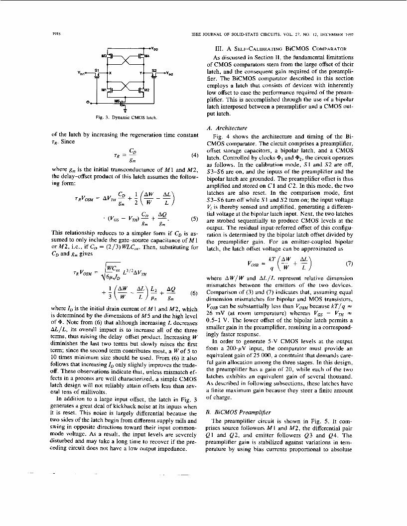
A. Architecture Fig. 4 shows the architecture and timing of the Bi-
CMOS comparator. The circuit comprises a preamplifier, offset storage capacitors, a bipolar latch, and a CMOS latch. Controlled by clocks and +2, the circuit operates as follows. In the calibration mode, S1 and S 2 are off, S 3 4 6 are on, and the inputs of the preamplifier and the bipolar latch are grounded. The preamplifier offset is thus amplified and stored on C 1 and C 2 . In this mode, the two latches are also reset. In the comparison mode, first S 3 4 6 turn off while S 1 and S2 turn on; the input voltage Vi is thereby sensed and amplified, generating a differen- tial voltage at the bipolar latch input. Next, the two latches are strobed sequentially to produce CMOS levels at the output. The residual input-referred offset of this configu- ration is determined by the bipolar latch offset divided by the preamplifier gain. For an emitter-coupled bipolar latch, the latch offset voltage can be approximated as
kT AW AL vOSB 7 (7 + t) (7)
where AW/ W and A L / L represent relative dimension mismatches between the emitters of the two devices. Comparison of (3 ) and (7) indicates that, assuming equal dimension mismatches for bipolar and MOS transistors, VOSB can be substantially less than VOSM because k T / q = 26 mV (at room temperature) whereas VGS - VTH = 0.5-1 V . The lower offset of the bipolar latch permits a smaller gain in the preamplifier, resulting in a correspond- ingly faster response.
In order to generate 5-V CMOS levels at the output from a 200-pV input, the comparator must provide an equivalent gain of 25 000, a constraint that demands care- ful gain allocation among the three stages. In this design, the preamplifier has a gain of 20, while each of the two latches exhibits an equivalent gain of several thousand. As described in following subsections, these latches have a finite maximum gain because they steer a finite amount of charge.
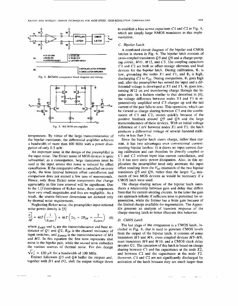
B. BiCMOS PreampliJier The preamplifier circuit is shown in Fig. 5. It com-
prises source followers M1 and M 2 , the differential pair Q l and Q 2 , and emitter followers Q3 and Q4. The preamplifier gain is stabilized against variations in tem- perature by using bias currents proportional to absolute
RAZAVI AND WOOLEY: DESIGN TECHNIQUES FOR HIGH-SPEED, HIGH-RESOLUTION COMPARATORS 1919
SlSZ OFF
LATCHES RESET .a1 .S?-SON
0 SI-SZ ON S3-56OFF LATCHES RESET
BIPOLAR LATCH STROBED 1 CMOS LATCH STROBED
Fig. 4. BiCMOS comparator block diagram and timing.
sc
Fig. 5 . BiCMOS preamplifier.
temperature. By virtue of the large transconductance of the bipolar transistors, the differential amplifier achieves a bandwidth of more than 1 0 0 MHz with a power dissi- pation of only 0.5 mW.
An important issue in the design of the preamplifier is the input noise. The flicker noise of MOS devices is quite substantial; as a consequence, large transistors must be used at the input unless this noise is reduced by offset cancellation. If the comparator offset is cancelled on every cycle, the time interval between offset cancellation and comparison does not exceed a few tens of nanoseconds. Hence, only those flicker noise components that change appreciably in this time interval will be significant. Due to the 1 /f dependence of flicker noise, these components have very small magnitudes and thus are negligible. As a result, the source-follower dimensions are dictated only by thermal noise requirements.
Neglecting flicker noise, the preamplifier input-referred noise power density is [5] -
1 ' = 4kT (-) + 4kT ( 2rb + 2Rsw + ~
Af gmBJT
where and rb are the transconductance and base re- sistance of Q 1 and Q 2 , Rsw is the channel resistance of input switches, and gmMOS is the transconductance of M 1 and M2. In this equation the first term represents shot noise in the bipolar pair, while the second term embodies the various sources of thermal noise. For this design
Emitter followers Q3 and Q4 buffer the outputs and, together with D 1 and 0 2 , shift the output voltage down
= 130 pV for a bandwidth of 100 MHz.
to establish a bias across capacitors C 1 and C2 in Fig. 4, which are simply large NMOS transistors in this imple- mentation.
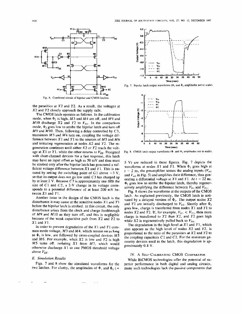
C. Bipolar Latch A combined circuit diagram of the bipolar and CMOS
latches is shown in Fig. 6. The bipolar latch consists of cross-coupled transistors Q5 and Q6 and a charge-pump- ing circuit, M11, M12, and C3. The coupling capacitors C1 and C2 act both as offset-storage elements and load devices for the bipolar latch. During calibration, is low, grounding the nodes X1 and Y 1 , and a2 is high, discharging C3 to VEE. During comparison, goes high and, after the preamplifier has sensed the input and a dif- ferential voltage is developed at X 1 and Y 1 , +2 goes low, turning M 12 on and transferring charge through the bi- polar pair. In a fashion similar to that described in [6], the voltage difference between nodes X1 and Y1 is re- generatively amplified until C3 charges up and the tail current of the pair falls to zero. This operation, which can be viewed as charge sharing between C3 and the combi- nation of C1 and C2, occurs quickly because of the positive feedback around Q5 and Q6 and the large transconductance of these devices. With an initial voltage difference of 1 mV between nodes X1 and Y 1 , the latch produces a differential voltage of several hundred milli- volts in less than 5 ns.
Since the bipolar latch steers charge, rather than cur- rent, it has two advantages over conventional current- steering bipolar latches: 1) it draws no input current dur- ing calibration and can therefore be directly coupled to C1 and C2 without input bias current cancellation, and 2) it has zero static power dissipation. Also, in this ap- plication the preamplifier need only attenuate the input offset resulting from the VBE mismatch of the two bipolar transistors Q 5 and Q6, rather than the larger V,, mis- match of two MOS devices as would be necessary if a CMOS latch were used.
The charge-sharing nature of the bipolar latch intro- duces a relationship between gain and delay that differs from that for current-steering circuits. In the latter the gain can approach infinity if sufficient time is permitted for re- generation, while the former has a finite gain because of the limited charge available for regeneration. The Appen- dix presents an analysis of transient response of the charge-steering latch to better illustrate this behavior.
D. CMOSLatch The last stage of the comparator is a CMOS latch, in-
cluded in Fig. 6, that is used to generate CMOS levels from the output of the bipolar latch. It consists of sense transistors M3 and M4, cross-coupled devices M 5 - M 8 , reset transistors M9 and M10, and a CMOS clock delay inverter G 1 . The operation of this latch is based on charge sharing between C l and the capacitance at the node X2, and between C2 and the capacitance at the node Y2. However, C1 and C2 are not significantly discharged by activation of the latch because they are much larger than
I920 IEEE JOURNAL OF SOLID-STATE CIRCUITS, VOL. 21, NO. 12. DECEMBER 1992
0 - Fig. 6. Combined circuit of bipolar and CMOS latches.
1 -
the parasitics at X 2 and Y 2 . As a result, the voltages at
The CMOS latch operates as follows. In the calibration mode, when 92 is high, M3 and M4 are off, and M9 and M 1 0 discharge X 2 and Y 2 to VEE. In the comparison mode, a2 goes low to strobe the bipolar latch and turn off M9 and M 1 0 . Then, following a delay controlled by C3, transistors M 3 and M4 turn on, coupling the voltage dif- ference between X 1 and Y 1 to the sources of MS and M 6
E -2
2 0
X 2 and Y 2 closely approach the supply rails.
g -3 - . 0 -
5 - 4 :
-5
-6
VXZ
- VY2
a 1 a 2
_ _ - . . . . . . . . .
5 ..._._._._._._._._.I- - \; \
................... c - - - - - 1 ' :'
>J. .?.
d' ' I ' ' ' " ' ' ' / I ' ' " " ' ' I I I I I I I ' ' ' ' I ' ' ' I ' ' ' I '
may have an input offset as high as 50 mV and thus must be strobed only after the bipolar latch has generated a suf- ficient voltage difference between X 1 and Y 1 . This is en- sured by setting the switching point of G 1 above - 3 V, so that its output does not go low until C3 has charged up by at least 2 V. Because C3 is approximately one-fifth the size of C 1 and C 2 , a 2-V change in its voltage corre- sponds to a potential difference of at least 200 mV be- tween X 1 and Y l .
Another issue in the design of the CMOS latch is the disturbance it may cause at the sensitive nodes X 1 and Y 1 before the bipolar latch is strobed. In this circuit, the only disturbance arises from the clock and charge feedthrough of M9 and M10 as they turn off, and this is negligible because of the weak capacitive path from X 2 and Y 2 to X 1 and Y 1 .
In order to prevent degradation of the X 1 and Y 1 com- mon-mode voltage, M3 and M4, which remain on as long as 4'2 is low, are followed by cross-coupled devices M5 and M6. For example, when X 2 is low and Y 2 is high MS turns off, isolating X1 from M 7 , which would otherwise discharge X 1 to one PMOS threshold voltage
5 V) are reduced in these figures. Fig. 7 depicts the waveforms at nodes X 1 and Y 1 . When 9, goes high at t = 2 ns, the preamplifier senses the analog inputs (Vjlinl and Vjn2 in Fig. 5 ) and amplifies their difference, thus gen- erating a differential voltage at X 1 and Y 1 . At t = 22 ns, G2 goes low to strobe the bipolar latch, thereby regener- atively amplifying the difference between Vx, and Vyl.
Fig. 8 shows the waveforms at the outputs of the CMOS latch. As explained previously, the CMOS latch is acti- vated by a delayed version of a2. The output nodes X 2 and Y 2 are initially discharged to VEE. Shortly after +2
goes low, charge is transferred from nodes X 1 and Y 1 to nodes X 2 and Y 2 . If, for example, Vxl < Vyl, then more charge is transferred to Y 2 than X 2 , and Y 2 goes high while X 2 is regeneratively pulled back to VEE.
The degradation in the high level at X 1 and Y 1 , which also appears as the high level of nodes X 2 and Y 2 , is proportional to the ratio of the parasitics at X 2 and Y 2 to the coupling capacitors C 1 and C 2 . For the minimum ge- ometry devices used in the latch, this degradation is ap- proximately 0.8 V.
- above VEE.
E. Simulation Results Figs. 7 and 8 show the simulated waveforms for the
two latches. For clarity, the amplitudes of 9, and a2 (=
IV. A SELF-CALIBRATING CMOS COMPARATOR While BiCMOS technologies offer the potential of su-
perior performance in both digital and analog circuits, many such technologies lack the passive components that

1921 RAZAVI AND WOOLEY: DESIGN TECHNIQUES FOR HIGH-SPEED, HIGH-RESOLUTION COMPARATORS
are essential for analog design. On the other hand, the prevalence of CMOS technology in system design has supported the incorporation of such components in many CMOS processes.
To improve the performance obtainable in a fully CMOS comparator, offset cancellation can be applied to both the preamplifier and the latch. The CMOS compar- ator described in this section employs a topology that achieves complete offset cancellation for both its pream- plifier and latch, thereby making it possible to achieve 12-b precision at comparison rates as high as 10 MHz when implemented in a 1-pm technology.
A. Architecture
Fig. 9 is a simplified block diagram of the CMOS com- parator. It consists of two transconductance amplifiers, G,, and Gm2, sharing the same output nodes, load resis- tors RL and RL2, and capacitors C 1 and C2 in a positive feedback loop around Gm2. In the offset-cancellation mode, the inputs of G,, and Gm2 are grounded and their offsets are amplified and stored on C1 and C 2 . In the comparison mode, the inputs are released from ground and the input voltage is sensed. This voltage is amplified by G,, to establish an imbalance at the output nodes A and B , and hence at the inputs of Gm2, initiating regeneration around Gm2.
The calibration of this comparator can be viewed as output offset storage applied to both G,,,, and Gm2, result- ing in complete cancellation of their offsets. This topol- ogy utilizes the offset-cancelled amplifier Gm2 for regen- eration, whereas a conventional 00s configuration incorporates an explicit latch that can suffer from large input offsets. Thus, neglecting second-order effects such as mismatch in charge injection from S5 and S 6 , the pro- posed topology achieves zero residual offset while retain- ing the advantages of 00s.
Owing to several complications, the block diagram of Fig. 9 is not practical if implemented directly as shown. First, the feedback capacitors and their parasitics load the output nodes, reducing the speed. Second, because of the finite on-resistance of S5 and S 6 , the positive feedback loop around Gm2 is not completely broken in calibration mode, making the circuit prone to oscillation. More im- portantly, when S5 and S 6 turn off to end the calibration, any mismatch in their charge injection can trigger a false regeneration around Gm2. Since the feedback is designed for a fast response, this regeneration may not be overrid- den by small voltages at the input, hence causing a large overall input-referred offset for the comparator. Fig. 10 illustrates a modified comparator configuration that cir- cumvents these problems. In this circuit, buffers B 1 and B 2 isolate nodes A and B from the feedback capacitors, while switches S 7 - S 10 disable the feedback loop when required. Regeneration begins only after the input voltage has been sensed and amplified. It should be noted that the offsets of B 1 and B 2 are also stored on C 1 and C2.
c1 - I 1 I 1
?ER,, s5 A =
d> 67 B
=
3% I 1 - c2
Fig. 9 . CMOS comparator simplified block diagram.
X
Y
X
Y
a, -1 0 0 S i , S3.9, S2, S5, S7-S10 S6 ON OFF
0 s1, s2, s9, si0 ON 0 S3-S8 OFF a2
Fig. 10. Modified CMOS comparator block diagram and timing
B. Circuit Details A CMOS implementation of the topology in Fig. 10 is
shown in Fig. 11. In this circuit, differential pairs M1, M 2 and M 3 , M4 constitute amplifiers G,, and Gm2, re- spectively, with source followers M 9 and M 10 serving as the buffers B1 and B 2 . Transistors M 7 and M 8 operate as active loads, while M 5 and M 6 set the output common- mode voltage and control the gain [2]. The additional cur- rents supplied by M 7 and M 8 both decrease the voltage drop across M 5 and M 6 and increase the available gain, two important advantages when the circuit must operate from a single 5-V supply. Moreover, by boosting the cur- rents that charge and discharge nodes A and B , the push- pull operation of M 3 with M 7 and M 4 with M 8 improves the large-signal response in two ways: it increases the out- put voltage swing and enhances the speed. This can be seen by noting that if, for example, node E goes high and node F goes low, the current in M 7 is reduced, thus al- lowing M 3 to more rapidly discharge node A to a lower voltage, while the current in M 8 is increased, thereby pulling node B more quickly to a higher voltage.
Since the comparator of Fig. 11 includes calibration of both the preamplifier and the latch, its residual offset is due primarily to mismatches among switches S5-S 10. Because of mismatches in their dimensions and threshold voltages, two nominally identical MOS devices carry slightly different charges in their inversion layers. This difference results in charge injection mismatch when the two switches turn off and charge absorption mismatch when they turn on. In the comparator circuit, both types of mismatch exist: charge injection mismatch from

S5-S8 when they turn off to end the calibration, and charge absorption mismatch from S9-S 10 when they turn on to establish a positive feedback loop around Gm2.
Because S5 and S 6 discharge their respective nodes to the same potential, their charge injection mismatch can be cancelled by an auxiliary switch placed between nodes E and F that turns off a few nanoseconds after S5 and S6, thereby equalizing the voltages at E and F [ 6 ] . With the same principle applied to S7 and S8, the charge absorp- tion mismatch between S9 and S 10 becomes the only sig- nificant contribution to the offset. This offset manifests itself when S9 and S10 turn on, absorbing charge from C1 and C2 into their channels. The charge absorption mismatch creates an offset voltage between the gates of M3 and M4 that is multiplied by the gain of the M3 and M4 pair when it appears at nodes A and B and is divided by the gain of the M1 and M2 pair when referred to the main input. The resulting input-referred offset is
(9)
where AQ is the channel-charge mismatch of S9 and S 10 when they are on, C = C1 = C2, and gm34, &78, and gmI2 are the transconductance values of differential pairs M 3 - M 4 , M7-M8, and Ml-M2, respectively. This equa- tion indicates that, for a given AQ, VOs can be reduced by: 1) increasing C, which increases the recovery and re- generation delays, as well as the area; 2) decreasing gm34 + &78, which is accomplished by decreasing 12 and not only degrades the regeneration speed but also lowers the output swing; and 3) increasing g m I 2 , which either in- creases the input capacitance (if M 1 and M2 are widened) or limits the input and output swings (if Z 1 is increased). As a compromise among these trade-offs, C = 0.5 pF and gmI2 = 2(gm3, + g,,,) were used in this design.
Equation (9) indicates that, in contrast to 00s and 10s configurations, the circuit in Fig. 1 1 imposes no con- straint between the preamplifier voltage gain and the re- sidual offset, thus allowing a better optimization of the load devices for speed and input range.
Since the flicker noise at the input of the comparator in Fig. 1 1 is removed by periodic offset cancellation, only thermal noise needs to be considered. If the noise contri- butions of source followers M9 and M10 and capacitors C 1 and C2 are neglected, the total input-referred thermal noise power density is
-
where gmij represents the transconductance of each device
in the pair Mi, 4. For this design, = 200 pV for a bandwidth of 80 MHz.
The comparator of Fig. 1 1 generates a differential out- put voltage of approximately 2 .6 V. A second CMOS latch-such as the one in the BiCMOS comparator de- scribed in Section 11-can be used to develop full CMOS levels from the differential output, as long as a carefully
* Fig. 11. CMOS comparator circuit diagram.
M 1 3 m V D D
Fig. 12. CMOS comparator output amplifier.
delayed phase of is used to properly time the regen- eration. A simpler approach is to employ a nonregenera- tive amplifier, such as the one shown in Fig. 12. Since the outputs X and Y of the comparator track the positive
spectively, the amplifier inputs cannot simply be refer- enced to ground because, under worst-case conditions of supply and process variations, the amplifier may not pro- vide rail-to-rail swings at its output. By replicating the X and Y common-mode voltage at the source of M17, the circuit in Fig. 12 generates pull-up currents in M13 and M14 that, during reset, are twice the pull-down currents in M 1 1 and M 12 if the latter two are driven from X and Y. In this case, Vol and Vo2 closely approach the supply rails. Since a single bias network, M 15-M 18, can be used for an array of comparators, the equivalent power dissi- pation of the output amplifier remains below 0.5 mW.
supply voltage by I VGs6I + vGs9 and I Vcs5I + ~ G ~ I o , re-
C. Simulation Results Simulated waveforms for the CMOS comparator are
shown in Figs. 13 and 14, wherein the amplitudes of al and a2 (= 5 V) have been reduced for clarity. Fig. 13 depicts the waveforms at nodes X and Y. At t = 2 ns, i9 , goes low and the preamplifier senses the analog inputs (Vinl and Vin2 in Fig. l l ) , amplifying their difference so as to produce a larger differential voltage at nodes X and Y. At t = 6 ns, a2 goes low to close the positive feedback
1922 IEEE JOURNAL OF SOLID-STATE CIRCUITS, VOL. 21, NO. 12, DECEMBER 1992

1923 RAZAVI AND WOOLEY: DESIGN TECHNIQUES FOR HIGH-SPEED, HIGH-RESOLUTION COMPARATORS
3.0 c
0)
= B g 1.5
5 1.0 L
a n
2.5
L 2.0
I' '. I
i \
-..-. , 0.5 -
0 . 0 ~ " " ~ " " ~ " " ~ " ' ~ ~ " " ~ " " ~ 0 5 10 15 20 25 30
400
350 [ - D. - CMOS Comparator
300
-0- BiCMOS Comparator
Time (nsec) Frequency (MHz)
Fig. 13. CMOS comparator output waveforms (a, and amplitudes not Fig. 15. Offset of comparators as a function of clock frequency to scale).
Fig. 14.
........ a2 1 ' ' , ~ 1 ' , , ' ~ , ' , ' ~ ' ' ' ~ ~ ' ' , ' 1 ' " / 1 0 5 10 15 20 25 30
Tlme (nsec) Output amplifier waveforms (+, and +2 amplitudes not to scale).
around Gm2, and V, - Vu is amplified regeneratively. At c = 16 ns, the comparator is reset and returns to the offset cancellation mode.
Fig. 14 shows the V,, and V,, waveforms of the output amplifier. For a small difference between V, and V,, V,, and VO2 are both high. When 1 Vx - Vy( is amplified to a few volts, I V,, - VO2l approaches full CMOS levels.
V. EXPERIMENTAL RESULTS The BiCMOS and CMOS comparators have been fab-
ricated in a 2-pm BiCMOS process [7] and a 1-pm CMOS process [8], respectively. The performance of these ex- perimental prototypes was evaluated for both dc and time- varying inputs. Typical measured input-referred offsets for two circuits are plotted as a function of the clock fre- quency in Fig. 15. The sharp variations in offset with fre- quency are attributed to ringing and clock coupling in the package and the test setup.
To demonstrate the effectiveness of the offset cancel- lation, as well as the overdrive recovery at 10 MHz, the circuit responses were also examined for dynamic inputs. The purpose of these tests is to verify that, at a 10-MHz comparison rate, the comparators can recover from a large differential input and subsequently detect a small differ- ential input. Fig. 16(a) depicts the experimental setup em- ployed for these tests [9]. In this circuit the differential
CLOCK. ; I
VA ......................................................... v, ....................................................... p -1 v I
V,
S1 CLOSED S1 OPEN
S2 CLOSED 52 OPEN
(b) Fig. 16. Overdrive recovery test: (a) setup, and (b) dynamic input.
waveform generated at the inputs of the comparator con- sists of a large voltage difference in one cycle and a small difference in the next. To generate this input signal the clock is divided in frequency by a factor of 2 and then applied to the bipolar differential pair Q l and Q 2 so that the voltage at node B remains low for one cycle and high for the next. The other input of the comparator is held at a dc voltage close to the high level at B . If the Q 1, Q2 pair completely switches the current I 1 , then the magni- tude and polarity of the small differential input that fol- lows the large transition can be precisely controlled by the value of RZ2 and the position of switches S 1 and S2. Two typical waveforms produced by this arrangement are il- lustrated in Fig. 16(b).
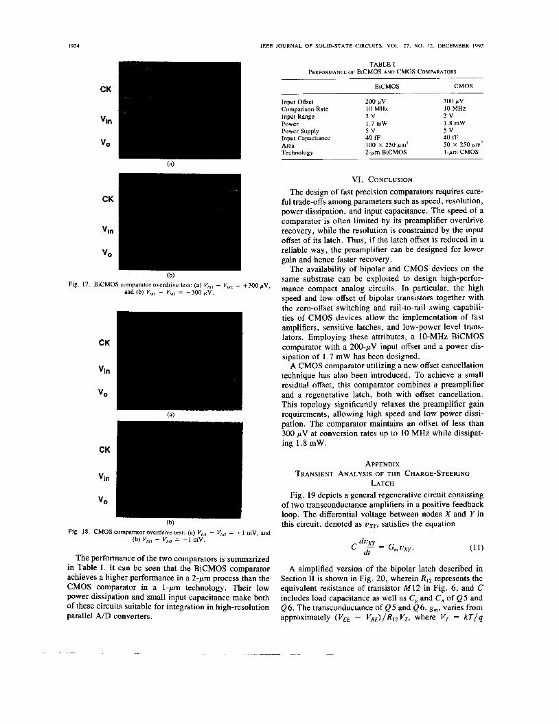
The oscillographs in Figs. 17 and 18 show that the comparators indeed accomplish full offset cancellation and overdrive recovery, yielding an output of one when (Knr
mV, and an output of zero when (Viinl - I/in2)BiCMOS = - 3 0 0 pV and (vnl - vn2)CMOS = -1 mV.
- I/inZ)BiCMOS = 4-300 p v and (Vinl - Vin2)CMOS = +1
1924 IEEE JOURNAL OF SOLID-STATE CIRCUITS, VOL. 27, NO. 12. DECEMBER 1992
TABLE I PERFORMANCE OF BiCMOS A N D CMOS COMPARATORS
CMOS BiCMOS CK Input Offset 200 p v 300 pV Comparison Rate 10 MHz 10 MHz
Vin Power 1.7 mW 1.8 mW
VO Area 100 x 250 pmZ 50 x 250pm’
Input Range 3 v 2 v
Power Supply 5 v 5 v Input Capacitance 40 fF 40 fF
Technology 2-pm BiCMOS l-pm CMOS
CK
Vin
VO
VI. CONCLUSION The design of fast precision comparators requires care-
ful trade-offs among parameters such as speed, resolution, power dissipation, and input capacitance. The speed of a comparator is often limited by its preamplifier overdrive recovery, while the resolution is constrained by the input offset of its latch. Thus, if the latch offset is reduced in a reliable way, the preamplifier can be designed for lower gain and hence faster recovery.
The availabilitv of bipolar and CMOS devices on the same substrate can be exploited to design high-perfor- mance compact analog circuits. In particular, the high Fig. 17. BiCMOS comparator overdrive test: (a) V,,, - V,n2 = +300 pV,
and (b) V. - , - V . , = -300 ,,v
CK
Vin
VO
CK
Vin
VO
~, ,111 ,,,,. - - - r - . .
speed and low offset of bipolar transistors together with the zero-offset switching and rail-to-rail swing capabili- ties of CMOS devices allow the implementation of fast amplifiers, sensitive latches, and low-power level trans- lators. Employing these attributes, a 10-MHz BiCMOS comparator with a 200-pV input offset and a power dis- sipation of 1.7 mW has been designed.
A CMOS comparator utilizing a new offset cancellation technique has also been introduced. To achieve a small residual offset, this comparator combines a preamplifier and a regenerative latch, both with offset cancellation. This topology significantly relaxes the preamplifier gain requirements, allowing high speed and low power dissi- pation. The comparator maintains an offset of less than 300 pV at conversion rates up to 10 MHz while dissipat- ing 1.8 mW.
APPENDIX TRANSIENT ANALYSIS OF THE CHARGE-STEERING
LATCH Fig. 19 depicts a general regenerative circuit consisting
of two transconductance amplifiers in a positive feedback loop. The differential voltage between nodes X and Y in this circuit, denoted as vxn satisfies the equation
Fig. 18. CMOS comparator overdrive test: (a) Vinl - V,.* = + 1 mV, and
ar The performance of the two comparators is summarized in Table I. It can be seen that the BiCMOS comparator achieves a higher performance in a 2-pm process than the CMOS comparator in a 1-pm technology. Their low power dissipation and small input capacitance make both of these circuits suitable for integration in high-resolution parallel A/D converters.
A simplified version of the bipolar latch described in Section I1 is shown in Fig. 20, wherein R 1 2 represents the equivalent resistance of transistor M12 in Fig. 6 , and C includes load capacitance as well as C, and C, of Q 5 and Q 6 . The transconductance of Q 5 and Q 6 , g,, varies from approximately (VEE - V B E ) / R 1 2 V T , where VT = k T / q

RAZAVI AND WOOLEY: DESIGN TECHNIQUES FOR HIGH-SPEED, HIGH-RESOLUTION COMPARATORS
X
1925
Y 1
Fig. 19. Regenerative amplifier.
X Y
f.’. TCB VEE
Fig. 20. Simplified circuit of bipolar latch.
(when M 12 turns on) to zero (when the drain current of M 12 falls to zero). Therefore, Q5 and Q6 cannot be sim- ply replaced with a small-signal equivalent circuit and (1 1 ) cannot be applied to this case. However, by deriving a time-dependent representation of g , and substituting it for G, in (1 l ) , an estimate of the equivalent gain of the latch can be obtained. A comparison of analytical results and SPICE simulations indicates that this approximation is in- deed representative of the latch’s behavior.
The current through R I 2 in Fig. 20, i D I 2 , can be ap- proximated as
If, for the moment, the base resistance of Q5 and Q 6 is neglected and /3 is assumed to be infinite, g, is approxi- mately
where r, is the emitter resistance of Q 5 and Q6. In (13) the collector currents of Q5 and Q 6 are assumed equal. Since this only holds for small vxy, the analysis is valid for amplification of very small signals, and in fact gives an upper bound for the equivalent gain of the latch.
Substituting (13) in (1 1) and rearranging terms yields
~ pyn ,,c,) Integrating both sides of this expression
dt t
re +
Since where uxyo is the initial imbalance applied to the latch.
16) = - - ln dt S a + b exp ( t / r ) a
(15) can be written as
/ --t 11
+ - exp - b r
The asymptotic equivalent gain of the circuit can be obtained by letting t -+ 03 in (17) and solving for uXY/ uxyo. For t = 00, the first term on the right-hand side of (17) vanishes; hence
where uxym is the final voltage difference between X and Y. The second term within the square brackets in (18) is typically less than 0.2. Since for small x, In (1 + x) = x - x 2 / 2 , (18) can be approximated accordingly to yield
The first exponential term in (19) represents the maximum available gain of the latch. The second term takes into account the effect of finite emitter resistance of Q5 and Q6 and, as simulations show, can also include base re- sistance rb by replacing re with’r, + rb//3. For typical values used in this design, (19) gives an asymptotic equivalent gain of approximately 8000 for the latch.
ACKNOWLEDGMENT The authors wish to thank Dr. P. Lim for his invaluable
comments. They are also indebted to Dr. J . Shott and the Stanford Integrated Circuits Laboratory staff for fabricat- ing the BiCMOS prototype, and to National Semiconduc- tor Corporation and L. Stoian for supporting this work and fabricating the CMOS prototype.
REFERENCES [ l ] R. Poujois et a l . , “Low-level MOS transistor amplifier using storage
techniques,” in ISSCC Dig. Tech. Papers, Feb. 1973, pp. 152-153. [2] J . Doemberg, P. R . Gray, and D. A . Hodges, “A 10-bit 5-Msample/s
CMOS two-step flash ADC,” IEEE J . Solid-State Circuits, vol. 24, pp. 241-249, Apr. 1989.
[3] D. J . Allstot, “A precision variable-supply CMOS comparator,” IEEE J . Solid-State Circuits, vol. SC-17, pp. 1080-1087, Dec. 1982.
[4] S. Chin, M . K. Mayes, and R . Filippi, “A multistep ADC family with efficient architecture,” in ISSCC Dig. Tech. Papers, Feb. 1989, pp. 16-17.

1926 IEEE JOURNAL OF SOLID-STATE CIRCUITS, VOL. 21, NO. 12, DECEMBER 1992
[51
161
171
WI
191
G. Erdi, “Amplifier techniques for combining low noise, precision, and high-speed performance,” IEEE J. Solid-Stare Circuits, vol. SC- 16, pp. 653-661, Dec. 1981. P. J. Lim and B. A. Wooley, “An 8-bit 200-MHz BiCMOS compar- ator,” IEEE J. Solid-State Circuits, vol. 25, pp. 192-199, Feb. 1990. J. Shott, C. Knorr, and M. Prisbe, “BiCMOS technology overview,” Stanford BiCMOS Project Tech. Rep., Center for Integrated Systems, Stanford Univ., Stanford, CA, Sept. 1990. T:l. Liou et al . , “A single-poly CMOS process merging analog ca- pacitors, bipolar and EPROM devices,” in Proc. VLSI Tech. Symp., May 1989, pp. 37-38. J. T. Wu and B. A. Wooley, “A 100-MHz pipelined CMOS compar- ator,” IEEE J. Solid-State Circuits, vol. 23, pp. 1379-1385, Dec. 1988.
Behzad Razavi (S’87-M’91) received the B.Sc. degree in electrical engineering from Tehran Uni- versity of Technology, Tehran, Iran, in 1985, and the M.Sc. and Ph.D. degrees in electrical engi- neering from Stanford University, Stanford, CA, in 1988 and 1991, respectively.
He worked at Tektronix, Inc., Beaverton, OR, during the summer of 1988 on the design of high- speed data acquisition systems, and he was a Re- search Assistant at the Center for Integrated Sys- tems, Stanford University, from 1988 to 1991.
Since December 1991 he has been a Member of the Technical Staff at AT&T Bell Laboratories, Holmdel, NJ, where he is involved in integrated circuit design in emerging technologies. His current interests include data acqui- sition systems, clock recovery circuits, low-voltage techniques, and lightwave communication circuits.
Bruce A. Wooley (S’H-M’70-SM’76-F’82) was born in Milwaukee, W1, on October 14, 1943. He received the B.S., M.S., and Ph.D. degrees in electrical engineering from the University of Cal- ifornia, Berkeley in 1966, 1968, and 1970, re- spectively.
From 1970 to 1984 he was a Member of the Research Staff at Bell Laboratories in Holmdel, NJ. In 1980 he was a Visiting Lecturer at the Uni- versity of Califomia, Berkeley. In 1984 he as- sumed his present position as Professor of Elec-
trical Engineering at Stanford University, Stanford, CA. His research is in the field of integrated circuit design and technology where his interests have included monolithic broad-band amplifier design, circuit architectures for high-speed arithmetic, analog-to-digital conversion, digital filtering, high-speed memory design, high-performance packaging and test systems, and high-speed instrumentation interfaces.
Prof. Wooley was the Editor of the IEEE JOURNAL OF SOLID-STATE CIR- CUITS from 1986 to 1989. He was the program Chairman of the 1990 Sym- posium on VLSI Circuits and the Co-chairman of the 1991 Symposium on VLSI Circuits. He was the Chairman of the 1981 Intemational Solid-state Circuits Conference, and he is a former Chairman of the IEEE Solid-state Circuits and Technology Committee. He has also served on the IEEE Solid- State Circuits Council and the IEEE Circuits and Systems Society Ad Corn. In 1986 he was a member of the NSF-sponsored JTECH Panel on Tele- communications Technology in Japan. He is a member of Sigma Xi, Tau Beta Pi, and Eta Kappa Nu. In 1966 he was awarded the University Medal by the University of California, Berkeley, and he was the IEEE Fortescue Fellow for 1966-1967.