Design Optimization Of Llc Topology And Phase Skipping ...
125
University of Central Florida University of Central Florida STARS STARS Electronic Theses and Dissertations, 2004-2019 2013 Design Optimization Of Llc Topology And Phase Skipping Control Design Optimization Of Llc Topology And Phase Skipping Control Of Three Phase Inverter For Pv Applications Of Three Phase Inverter For Pv Applications Utsav Somani University of Central Florida Part of the Electrical and Electronics Commons Find similar works at: https://stars.library.ucf.edu/etd University of Central Florida Libraries http://library.ucf.edu This Masters Thesis (Open Access) is brought to you for free and open access by STARS. It has been accepted for inclusion in Electronic Theses and Dissertations, 2004-2019 by an authorized administrator of STARS. For more information, please contact [email protected]. STARS Citation STARS Citation Somani, Utsav, "Design Optimization Of Llc Topology And Phase Skipping Control Of Three Phase Inverter For Pv Applications" (2013). Electronic Theses and Dissertations, 2004-2019. 2885. https://stars.library.ucf.edu/etd/2885
Transcript of Design Optimization Of Llc Topology And Phase Skipping ...

University of Central Florida University of Central Florida
STARS STARS
Electronic Theses and Dissertations, 2004-2019
2013
Design Optimization Of Llc Topology And Phase Skipping Control Design Optimization Of Llc Topology And Phase Skipping Control
Of Three Phase Inverter For Pv Applications Of Three Phase Inverter For Pv Applications
Utsav Somani University of Central Florida
Part of the Electrical and Electronics Commons
Find similar works at: https://stars.library.ucf.edu/etd
University of Central Florida Libraries http://library.ucf.edu
This Masters Thesis (Open Access) is brought to you for free and open access by STARS. It has been accepted for
inclusion in Electronic Theses and Dissertations, 2004-2019 by an authorized administrator of STARS. For more
information, please contact [email protected].
STARS Citation STARS Citation Somani, Utsav, "Design Optimization Of Llc Topology And Phase Skipping Control Of Three Phase Inverter For Pv Applications" (2013). Electronic Theses and Dissertations, 2004-2019. 2885. https://stars.library.ucf.edu/etd/2885

DESIGN OPTIMIZATION OF LLC TOPOLOGY AND PHASE SKIPPING CONTROL OF THREE PHASE INVERTER FOR PV APPLICATIONS
by
UTSAV SOMANI B.S. University of Pune, India, 2010
A thesis submitted in partial fulfillment of the requirements for the degree of Master of Science
in the Department of Electrical Engineering and Computer Science in the College of Engineering and Computer Science
at the University of Central Florida Orlando, Florida
Summer Term 2013
Major Professor: John Shen and Issa Batarseh

ii
© 2013 Utsav Somani

iii
ABSTRACT
The world is heading towards an energy crisis and desperate efforts are being made to
find an alternative, reliable and clean source of energy. Solar Energy is one of the most
clean and reliable source of renewable energy on earth. Conventionally, extraction of
solar power for electricity generation was limited to PV farms, however lately Distributed
Generation form of Solar Power has emerged in the form of residential and
commercial Grid Tied Micro-Inverters. Grid Tied Micro-Inverters are costly when
compared to their string type counterparts because one inverter module is required for
every single or every two PV panels whereas a string type micro-inverter utilizes a
single inverter module over a string of PV panels. Since in micro-inverter every panel
has a dedicated inverter module, more power per panel can be extracted by performing
optimal maximum power tracking over single panel rather than over an entire string of
panels. Power per panel extracted by string inverters may be lower than its maximum
value as few of the panels in the string may or may not be shaded and thereby forming
the weaker links of the system.
In order to justify the higher costs of Micro-Inverters, it is of utmost importance to
convert the available power with maximum possible efficiency. Typically, a micro-
inverter consists of two important blocks; a Front End DC-DC Converter and Output DC-
AC Inverter. This thesis proposes efficiency optimization techniques for both the blocks
of the micro-inverter.

iv
Efficiency Optimization of Front End DC-DC Converter
This thesis aims to optimize the efficiency of the front end stage by proposing optimal
design procedure for resonant parameters of LLC Topology as a Front End DC-DC
Converter for PV Applications. It exploits the I-V characteristics of a solar panel to
design the resonant parameters such that resonant LLC topology operates near its
resonant frequency operating point which is the highest efficiency operating point of
LLC Converter.
Efficiency Optimization of Output DC-AC Inverter
Due to continuously variable irradiance levels of solar energy, available power for
extraction is constantly varying which causes the PV Inverter operates at its peak load
capacity for less than 15% of the day time. Every typical power converter suffers
through poor light load efficiency performance because of the load independent losses
present in a power converter. In order to improve the light load efficiency performance
of Three Phase Inverters, this thesis proposes Phase Skipping Control technique for
Three Phase Grid Tied Micro-Inverters. The proposed technique is a generic control
technique and can be applied to any inverter topology, however, in order to establish
the proof of concept this control technique has been implemented on Three Phase Half
Bridge PWM Inverter and its analysis is provided. Improving light load efficiency helps to
improve the CEC efficiency of the inverter.

v
Dedicated to my Late Grandfather
Shri. Nandlal Jechand Somani

vi
ACKNOWLEDGMENTS
I have always believed that whatever we have; is what we have earned. It is our hard
work that would help us grow and nothing else. However, my experience during my
days at Florida Power Electronics Center has led me to make an amendment in my
beliefs which is that apart from one’s hard work and initiative, it is the support from your
family, friends, colleagues and teachers that helps you achieve different milestones in
life. I would like to use this space to express my gratitude to all those people who
directly or indirectly have helped me to achieve on of the milestones of my life.
First of all, I would like to thank Dr. John Zheng Shen & Dr. Issa Batarseh for giving me
an opportunity to contribute to this highly distinguished research group. I am deeply
grateful to my seniors, Lin Chen and Dr. Haibing Hu, whose positive recommendations
helped me secure a position of Research Assistant at Florida Power Electronics Center.
It was a great honor to be a part of such an elite research group.
I am highly grateful to my other senior colleagues Anna Grishina, Ahmadreza
Amirahmadi, Dr. Qian Zhang and Dr. Xiang Fang for being patient and helping me
throughout my time at FPEC. All the skills that I have acquired at FPEC; my colleagues
have played a major role in helping me acquire them. I would also like to thank my
supervisor Jesus Barrios for helping me to learn different lab equipment and develop
the right laboratory practices while performing experiments.

vii
I am thankful to my committee members Dr. Issa Batarseh, Dr. Thomas Wu and Dr.
Alireza Seyedi who gave me their guidance, support and their expert judgment during
the completion of my thesis.
Of all the people we meet in our lifetime, there are only a handful people to whom you
can give the title Guru. I have been very fortunate to meet one such person at FPEC in
such an early phase of my life, my true mentor, Charles Jourdan. I cannot thank him
enough for being ridiculously patient with me during the course of my Master’s Thesis.
Everything I learnt about Power Electronics Design at FPEC, I owe it to him.
Another such a pair of Gurus which I was endowed with by birth is my parents. All of my
achievements are the culmination of qualities like honesty, perseverance and sincerity
which I tried to inherit from my parents. No words can measure the sacrifice and hard
work of theirs in making me the person who I am today.
Finally, I am grateful to family, friends, special friends and every single person who has
nurtured, educated and supported me.

viii
TABLE OF CONTENTS
LIST OF FIGURES ......................................................................................................... xii
LIST OF TABLES .......................................................................................................... xvi
CHAPTER 1: INTRODUCTION ....................................................................................... 1
1.1 Global Energy Trends ........................................................................................ 1
1.2 Renewable Energy Trends ................................................................................. 4
1.3 Solar Power Trends ........................................................................................... 5
1.4 Types of PV Systems ......................................................................................... 7
1.4.1 Off Grid PV Systems (Standalone PV Systems). ......................................... 7
1.4.2 Grid Tied PV Systems ................................................................................. 8
1.5 Grid Tie Inverter Architectures ......................................................................... 10
1.5.1 Central Type Inverters ............................................................................... 10
1.5.2 String Type Inverter ................................................................................... 12
1.5.3 Multi-String Type Inverter .......................................................................... 14
1.5.4 AC Module Type Inverter – Micro-Inverters ............................................... 15
1.6 Comparative Review of Existing Single Phase Micro-Inverters in the market .. 17
1.7 Micro-Inverters for Three Phase Applications .................................................. 19
1.7.1 Existing 3 Phase Configurations using Single Phase Micro-inverters ........ 19
1.8 Three Phase Micro-Inverter ............................................................................. 21

ix
1.9 Objective and Outline of the Thesis ................................................................. 23
1.10 References ................................................................................................... 25
CHAPTER 2: DESIGN OPTIMIZATION OF LLC TOPOLOGY FOR PV APPLICATIONS
...................................................................................................................................... 27
2.1 PV Panel Characteristics ................................................................................. 28
2.1.1 Observations from Solar Panel’s I-V and P-V Curves: .............................. 33
2.2 Full Bridge LLC Resonant Converter: .............................................................. 33
2.2.1 LLC Converter FHA Analysis ..................................................................... 35
2.2.2 Operating Modes of LLC Converter ........................................................... 39
2.2.3 Discussion on Design considerations of LLC Converter as front end DC-DC
Converter of Micro-Inverter .................................................................................... 48
2.3 Design Procedure for Resonant Parameters of LLC Converter as Front End
DC-DC Converter of Micro-inverter ............................................................................ 50
2.3.1 Deriving the Design Specifications ............................................................ 50
2.3.2 Calculating Resonant Parameters ............................................................. 51
2.3.3 Design Example ........................................................................................ 54
2.4 References ....................................................................................................... 58
CHAPTER 3: LIGHT LOAD EFFICIENCY IMPROVEMENT OF THREE PHASE GRID
TIED INVERTERS......................................................................................................... 60

x
3.1 Daily Solar Irradiance Pattern .......................................................................... 60
3.2 Significance of Weighted Efficiency for PV Inverters ........................................ 64
3.3 Efficiency Behavior in Power Converters ......................................................... 66
3.4 Half Bridge PWM Inverter ................................................................................ 69
3.4.1 Half Bridge Inverter Operation: .................................................................. 71
3.4.2 Loss Analysis of Half Bridge Inverter: ........................................................ 78
3.4.3 Loss Model of Half Bridge Inverter: ........................................................... 84
3.4.4 Verification of Loss Model .......................................................................... 87
3.5 Phase Skipping Control of Three Phase Micro-Inverter ................................... 91
3.5.1 Concept ..................................................................................................... 91
3.5.2 Implementation of Phase Skipping Control for Three Phase Grid Tied
Micro-Inverters ....................................................................................................... 93
3.5.3 Experimental Results of Phase Skipping Control ...................................... 95
3.5.4 Avoiding Phase Power Imbalance due to Phase Skipping ........................ 98
3.6 References ..................................................................................................... 100
CHAPTER 4: CHAPTER FOUR: CONCLUSIONS AND FUTURE WORK .................. 103
4.1 Conclusions.................................................................................................... 103
4.2 Future Work ................................................................................................... 107
4.2.1 Future Work for LLC Converter as front end DC-DC Converter .............. 107

xi
4.2.2 Future Work for Phase Skipping Control ................................................. 108

xii
LIST OF FIGURES
Figure 1-1 Impact of Population and GDP on Global Energy Demand ........................... 2
Figure 1-2 Trends of Shares of World Primary Energy ................................................... 3
Figure 1-3 Global New Investment in Renewable Energy: Developed vs Developing
Countries, 2004-2011, $BN Source: Bloomberg New Energy Finance ........................... 4
Figure 1-4 Global New Investment in Renewable Energy by Sector, 2011, And Growth
on 2010, $BN. ................................................................................................................. 5
Figure 1-5 Off Grid PV System Architecture .................................................................... 7
Figure 1-6 Grid Tie PV System ....................................................................................... 9
Figure 1-7 Central Type PV Inverter Architecture ......................................................... 11
Figure 1-8 String Type Inverter Architecture ................................................................. 13
Figure 1-9 Multi-String Type Inverter ............................................................................. 14
Figure 1-10 AC Module Type Inverter Architecture ....................................................... 15
Figure 1-11 Single Phase Micro-Inverter Connected to Three Phase Grid ................... 20
Figure 1-12 Block Diagram of Three Phase Micro-Inverter ........................................... 21
Figure 2-1 Block Diagram - Grid Tied Micro-Inverter ..................................................... 27
Figure 2-2 Single Diode Equivalent Model of PV Panel ................................................ 29
Figure 2-3 I-V & PV Characteristics of PV Panel ........................................................... 30
Figure 2-4 I-V Curves of Solar Panel with Varying Temperature and Irradiance Level . 31
Figure 2-5 P-V Curves of Solar Panel with Varying Temperature and Irradiance Level 32
Figure 2-6 Block Diagram of Resonant Converter Topology ......................................... 34
Figure 2-7 Full Bridge LLC Converter ............................................................................ 35

xiii
Figure 2-8 AC Equivalent Circuit of LLC Converter ....................................................... 36
Figure 2-9 Derivation of AC Equivalent Impedance ...................................................... 36
Figure 2-10 LLC Converter Gain Curves (Ln=2) ........................................................... 38
Figure 2-11 Waveforms for Zone 1- fco≤fsw≤fo ................................................................ 41
Figure 2-12 Equivalent Circuits of Operation Modes of LLC Converter in Zone 1 -
fco≤fsw≤fo ........................................................................................................................ 42
Figure 2-13 Waveforms of Zone 2- fsw=fo ...................................................................... 44
Figure 2-14 Waveforms of Zone 3 – fsw>fo .................................................................... 46
Figure 2-15 Equivalent Circuits of Operation Modes of LLC Converter in Zone 3 - fsw>fo
...................................................................................................................................... 47
Figure 2-16 Optimal Design Consideration for LLC Converter as front DC-DC converter
of Micro-Inverter ............................................................................................................ 49
Figure 2-17 Normalized Gain, M vs Quality Factor, Qe ................................................. 52
Figure 2-18 Gain vs Switching Frequency-Fixed Qe-Variable Ln .................................. 53
Figure 2-19 Full Bridge LLC Converter as Front End DC-DC Converter for Micro-
Inverter .......................................................................................................................... 54
Figure 2-20 Gain vs. Switching Frequency, Design Example ........................................ 56
Figure 2-21 PV Panel Power vs. Switching Frequency for LLC Converter as front end
DC-DC Converter, design example ............................................................................... 57
Figure 2-22 Experimental Results - Efficiency, design example .................................... 57
Figure 3-1 Solar Irradiance Pattern on a Typical Day.................................................... 60
Figure 3-2 Solar Irradiance Patterns – Clear Days ........................................................ 62

xiv
Figure 3-3 Solar Irradiance Curves – Cloudy Days ....................................................... 63
Figure 3-4 Efficiency Curve of a Typical Power Converter ............................................ 66
Figure 3-5 Impact of Losses as a Function of Load Current on Efficiency .................... 68
Figure 3-6 Comparison of Synchronous Buck Converter and Half Bridge Inverter ....... 69
Figure 3-7 Gate Drive Signal for Half Bridge Inverter .................................................... 70
Figure 3-8 Half Bridge Inverter - Operation Modes - Topology ...................................... 75
Figure 3-9 Half Bridge Inverter - Operation Mode Waveforms - Positive Half Cycle ..... 76
Figure 3-10 Half Bridge Inverter - Operation Mode Waveforms- Negative Half Cycle ... 77
Figure 3-11 Half Bridge Inverter - With Drive Circuit ..................................................... 78
Figure 3-12 MOSFET Switching Waveform .................................................................. 80
Figure 3-13 Diode Reverse Recovery Waveforms ........................................................ 81
Figure 3-14 Load Independent Losses based on Loss Model, design example ............ 88
Figure 3-15 Load Dependent Losses based on Loss Model, design example. ............. 89
Figure 3-16 Losses in Half Bridge Inverter, design example ......................................... 89
Figure 3-17 Efficiency of Half Bridge Inverter - Loss Model Calculated vs. Experimental
...................................................................................................................................... 90
Figure 3-18 Half Bridge Three Phase PWM Inverter ..................................................... 90
Figure 3-19 Conceptual Diagram - Normal Mode - Phase Skipping Mode .................... 92
Figure 3-20 Implementation of Phase Skipping Control Scheme- Singe Stage ............ 94
Figure 3-21 Flow Chart of Phase Skipping Control Algorithm-Single Stage .................. 94
Figure 3-22 Prototype of 400W Three Phase Micro-Inverter ......................................... 96
Figure 3-23 Schematic of Three Phase Micro-Inverter .................................................. 96

xv
Figure 3-25 Operational Waveforms of Phase Skipping Control ................................... 97
Figure 3-26 Three Phase Half Bridge Inverter Efficiency with Phase Skipping Control *
...................................................................................................................................... 98
Figure 3-27 Avoiding Power Imbalance amongst Phases due to Phase Skipping Control
– Concept .................................................................................................................... 100

xvi
LIST OF TABLES
Table 1-1Specifications of the existing Single Phase Micro-Inverters ........................ 1-18

1
CHAPTER 1: INTRODUCTION
The biggest quest on which mankind has embarked upon in the 21st Century is to
identify cheap and reliable source of energy. Industrialization has led to an exponential
increase in global energy demands. Since the dawn of industrial revolution, fossil fuels
have been a dominant source of energy. However, the limited availability of fossil fuels
and the environmental hazards caused due to CO2 emissions due to burning of these
fossil fuels has further propelled mankind to identify alternative cleaner and sustainable
sources of energy.
1.1 Global Energy Trends
The two key drivers of global energy demand are rise in Population and Income. British
Petroleum in their annual energy outlook [1.1], predict that by 2013 the global
population will increase by 1.3 Billion and thereby making the total global population of
8.3 Billion. The global GDP is expected to roughly double the 2011 level in real terms by
2030. Due to this increase in population and GDP, the world energy demand is
projected to grow by 1.6% p.a. from the year 2011 to 2030 thereby leading to 36%
increase in global energy consumption by 2030. Figure 1-1 [1.1], shows that global
population and GDP have similar trend as of global energy demand. In this figure, the
statistics are presented from the countries belonging to set of groups.
1. OECD (Organization for Economic Co-operation and Development )
2. Non-OECD.

2
90% of the total population growth will be contributed by low and medium income
economies outside the OECD. The non OECD economies will undergo rapid
industrialization, urbanization and motorization which will lead them to contribute to 70%
of the total GDP growth and over 90% of the global energy demand growth by the year
2030 [1.1].
Figure 1-1 Impact of Population and GDP on Global Energy Demand
In order to achieve the goal of limiting global warming to 2⁰C, the consumption of fossil
fuels prior to 2050 should not be more than one third of proven reserves of fossil fuels
[1.2]. This leaves the world only with two choices viz. Nuclear Energy and Renewable
Energy in order to meet their energy demands. The Fukushima Nuclear Plant Disaster
which occurred in Japan in 2011 has led many countries to review their policies towards
nuclear energy due to their safety concerns.

3
Figure 1-2 Trends of Shares of World Primary Energy
From Figure 1-2 it can be concluded that consumption of fossil fuels with high CO2
emissions like coal and oil are predicted to fall. The trend of nuclear energy shows that
it has crossed a tipping point and is expected to observe a growth with caution due to
their safety concerns. The trends project Renewable Energy to have the highest growth
rate in the share of World Primary Energy.

4
1.2 Renewable Energy Trends
Renewable energy is the forerunner in the search of a cleaner and safer source of
energy. A steady rise in the hydropower, wind and solar installations has made
renewable energy an essential contributor in meeting the global energy demand.
International Energy Agency estimates that by 2035 renewable energy would account
for almost 1/3rd of the total electricity production. This speedy rise in renewable energy
is further propelled by increasing prices of fossil fuels and carbon pricing, falling
technology costs of renewable energy and most importantly, by the subsidies offered.
Global subsidies for renewable energy are expected to rise from $88 billion in 2011 to a
staggering $240 billion by 2035[1.2].
Figure 1-3 Global New Investment in Renewable Energy: Developed vs Developing Countries, 2004-2011, $BN
Source: Bloomberg New Energy Finance

5
1.3 Solar Power Trends
Solar Energy is emerging to be the fastest growing source of renewable energy. Wind
energy was considered to be one of the most mature renewable power technologies.
However in 2011, solar took a lead in the race by attracting twice as much investment
as wind. Investment in solar power observed an increase by 52% to $147 billion
whereas investment in wind power grew by only 12% to $84 billion [1.4].
Figure 1-4 Global New Investment in Renewable Energy by Sector, 2011, And Growth on 2010, $BN.
New investment volume adjusts for re-invested equity. Total values include estimates of undisclosed deals. Source: Bloomberg New Energy Finance, UNEP
One of the key economic factors which led to growth in investment in solar power is the
falling in technology costs of solar power. Photovoltaic module prices fell by almost 50%
in the year 2011[1.3]. By the end of 2011, the PV modules prices were dropped

6
between $1 and $1.20 per watt which was approximately 76% below their prices during
summer of 2008. Apart from the economic benefits, the other factors which makes solar
energy more investment friendly according to [1.4][1.5] are:
No moving parts hence low maintenance.
No water need.
Noiseless operation.
No hazardous emissions.
Scalable for any capacity of power requirement.
Flat construction allowing them to be implemented the building rooftops.
Long Lifetimes.
Highly suitable for distributed power generation.
Peak solar power generation coincides with peak energy demanded.

7
1.4 Types of PV Systems
PV systems are classified based on their power delivery system, type of load driven and
the storage elements present in the PV system. The type of PV system adopted also
depends on the functional requirements of the power delivery system. PV systems are
broadly classified into following 2 categories.
1. Off Grid PV Systems (Standalone PV Systems).
2. Grid Tie PV Systems.
1.4.1 Off Grid PV Systems (Standalone PV Systems).
Off Grid PV System invert the DC solar power into AC power to drive the AC loads
connected. They are equipped with battery storage. This battery storage is used to store
the surplus power available during the day. This stored power is used to drive the loads
during low light conditions or night time. Figure1- 5 shows the architecture of Off Grid
PV System.
Figure 1-5 Off Grid PV System Architecture

8
Advantages:
Independent of Grid.
No need to inject power in sync with utility grid.
Does not inject any instability in the utility grid.
No anti-islanding issues.
Able to provide power to rural areas where there is no utility grid.
Disadvantages:
Cost of battery makes the system expensive.
Additional cost of battery charger.
No incentives or tax credits.
Once the batteries are fully charged, the excess available power is wasted.
Power conversion losses occur while storing the power in batteries and while
converting the stored power back into AC power.
1.4.2 Grid Tied PV Systems
Grid Tied PV systems inject the solar power into utility grid which in turn drives the load
connected on the grid. It is one of the key power sources in Distributed Generation (DG)
Power System. Grid Tie PV system is the most popular and widely adopted PV system.
It eliminates the need of storage unit thereby reducing the cost dramatically. This PV
system is most suitable for residential, commercial and PV farm applications. Figure 1-6
shows the architecture of Grid Tie PV system.

9
Figure 1-6 Grid Tie PV System
Advantages:
No need of energy storage.
Amount of excess power injected into grid is accounted for and credited into
utility bill.
No storage losses.
Easy installation.
Higher Power density due to absence of energy storage.
Disadvantages:
Requires synchronization with the grid.
Requires anti-islanding.
Grid operators need to achieve balance between load and generated power.
Varying injected power tends to create instability into the grid.

10
1.5 Grid Tie Inverter Architectures
Grid Tie Inverters can be classified into different architectures depending upon the
manner in which the power is processed from solar panels to the utility grid. Grid Tie
PV Inverter architecture is classified as follows [1.6]:
1. Central Type Inverters.
2. String Type Inverters.
3. Multi-String Type Inverters.
4. AC Module Type Inverter / Micro-Inverter
1.5.1 Central Type Inverters
In this architecture large number of PV panels are interfaced together in a series to form
a string. The number of PV panels in this string is selected such that total series DC
voltage at the output of each string is high enough that no further amplification is
needed. Many such strings are connected together in parallel using series using
blocking diodes and fed to a central DC-AC inverter. Figure 1-7 shows the architecture
of Central Type PV Inverter. The central inverter performs the maximum power point
tracking for all the panels collectively.

11
Figure 1-7 Central Type PV Inverter Architecture
Advantages:
Economical architecture for large PV farms.
Higher weighted efficiency of central inverter due to high input voltage levels.
Disadvantages [1.7]:
High voltage DC cables PV Panels and inverter.
High DC voltages may lead to arcing.
Losses due to mismatch between PV panels
Centralized maximum power point tracking (MPPT) leads to power losses.
Losses in string blocking diodes.
Non flexible design due to which cost effectiveness of mass production cannot
be attained.
Grid connected stage is usually line commutated by thyristors which lead to
generation of current harmonics and thereby poor power quality.

12
Lack of redundancy - Failure of the central inverter brings down the entire PV
farm.
Central inverter needs to be kept in a protected environment due to large power
capacity which further increases the cost.
Central Type inverters are not easily scalable thereby each PV farm needs a
custom design depending upon its power capacity.
1.5.2 String Type Inverter
String Type inverter architecture can be considered to be the modular version of Central
Type Inverter. A large numbers of PV panels are connected in series to form a string.
Each of these string are fed to an individual DC-AC inverter which performs maximum
power point tracking and inverts the DC power from PV panel string into AC power and
injects into the utility grid. Similar to central type inverter, in string inverter each string
generates DC voltage high enough such that no further need of amplification is needed.
Figure 1-8 shows the architecture of String Inverter.
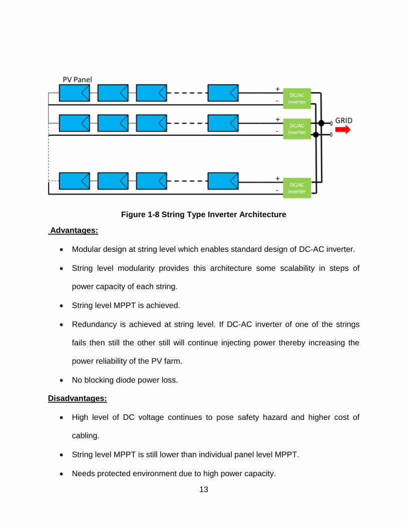
13
Figure 1-8 String Type Inverter Architecture
Advantages:
Modular design at string level which enables standard design of DC-AC inverter.
String level modularity provides this architecture some scalability in steps of
power capacity of each string.
String level MPPT is achieved.
Redundancy is achieved at string level. If DC-AC inverter of one of the strings
fails then still the other still will continue injecting power thereby increasing the
power reliability of the PV farm.
No blocking diode power loss.
Disadvantages:
High level of DC voltage continues to pose safety hazard and higher cost of
cabling.
String level MPPT is still lower than individual panel level MPPT.
Needs protected environment due to high power capacity.
14
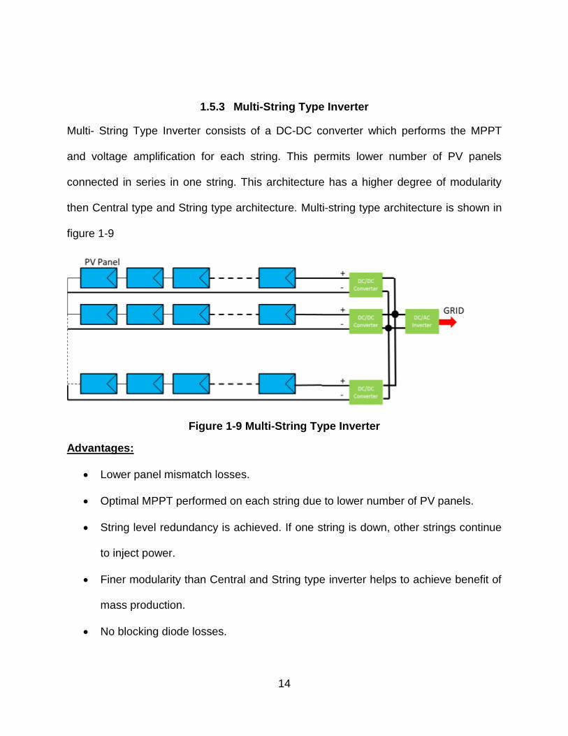
1.5.3 Multi-String Type Inverter
Multi- String Type Inverter consists of a DC-DC converter which performs the MPPT
and voltage amplification for each string. This permits lower number of PV panels
connected in series in one string. This architecture has a higher degree of modularity
then Central type and String type architecture. Multi-string type architecture is shown in
figure 1-9
Figure 1-9 Multi-String Type Inverter
Advantages:
Lower panel mismatch losses.
Optimal MPPT performed on each string due to lower number of PV panels.
String level redundancy is achieved. If one string is down, other strings continue
to inject power.
Finer modularity than Central and String type inverter helps to achieve benefit of
mass production.
No blocking diode losses.

15
Disadvantages:
Although the size of string is reduced, still the DC output voltage of each string is
high enough to be considered to be hazardous.
MPPT is still lower than individual panel level MPPT.
1.5.4 AC Module Type Inverter – Micro-Inverters
AC Module Type Inverter is an integration of PV Panel with an inverter. In this
architecture each PV panel has a dedicated AC module which performs MPPT, DC
voltage amplification and inversion. AC Module Type Inverter is the smallest grid
connected PV system unit [1.8] hence, it is also known as Micro-Inverter. Due to high
level of modularity which can be achieved in this architecture, installation of these
inverters does not require any knowledge of electrical installations. AC Module Type
Inverter architecture is shown in Figure 1-10.
Figure 1-10 AC Module Type Inverter Architecture

16
Advantages [1.6] [1.7]:
Lower cost per unit achieved due to benefits of mass production.
High Reliability - As each PV panel has its independent inverter, if one of the
inverter fails then all the other inverter continues to power the PV farm without
any significant loss of power.
Minimum Down Time – Once a faulty module is identified, it can be easily
replaced by a new module due to its Plug N Play nature, thereby reducing down
time.
Simpler System Design.
Mismatch losses between PV modules are completely eliminated as there is only
one panel per inverter.
Optimal MPPT is achieved as each PV panel has its dedicated MPPT controller.
High Scalability – Due to modular nature of the AC Module Type Inverter, this
architecture can be easily scaled to the required power capacity.
Higher Safety – There are no hazardous high voltage cables.
Disadvantages:
High voltage amplification required at every panel reduces the overall efficiency.
Increase in price per watt due to more complex circuit topologies performing
MPPT, DC voltage amplification and inversion.

17
1.6 Comparative Review of Existing Single Phase Micro-Inverters in the market
In order to understand the existing trends in the micro-inverter designs; side by side
comparison of micro-inverters from leading manufacturers based on their specifications
were done. Table 1-1 summarizes the design specifications of the micro-inverters
manufactured by the following six major manufacturers based on the public data:
1. Solar Bridge.
2. Enecsys.
3. Enphase.
4. Power One.
5. SMA.
6. Petra Solar.
By comparing the design specifications of Table 1, following observations can be made
about the current trends of the micro-inverters.
1. Most of the micro-inverters have power ratings of 200~300W as wide number of
PV panel manufacturers have PV panels in this power range. Enecsys SMI-
D240W-60-UL which consists of two PV panels connected in parallel at the input
of the micro-inverter has a power rating of 450W.
2. Nominal output voltage and frequency ratings vary according to the regional
standards.
3. Weighted efficiency is higher than 93%.
4. Micro-inverters incorporate communication capability with a central server for
diagnostics and monitoring purposes.

1-18
Table 1-1Specifications of the existing Single Phase Micro-Inverters
Solar Bridge-
Pantheon2
Enecsys Enphase Power One SMA Petra Solar
60Hz 50Hz(P
250LV-
230AU)
SMI-
S240W-
60-UL
SMI-
D240W-60-
UL
240-60-MP 300-60-MP 0.25-I-
OUTD
0.3-I-
OUTD
Sunny
Boy 240
US
SEM120
Output Power -
Active- (Watts)
238 238 225 450 240 300 215 250 300 240 200
Output Power-
Reactive- (VAR)
NA NA NA NA NA +/-200
Nominal Output
Voltage (V)
240 230 240 240 230 240 230 240 240/208 240/208 240 120
Nominal Output
Frequency(Hz)
60 50 60 60 50 60 50 60 60 60 60 60
Power Factor >0.99 >0.99 >0.95 >0.95 >0.95 >0.95 >0.95 >0.95 NA NA
Peak Efficiency
(%)
95.7 95.6 95 96 96.4 96.5 96.4 96.5 96.3 96.5 95.5 NA
Weighted
Efficiency (%)
95
(CEC)
93.2(E
URO)
93(CEC) 94.5(CEC) 95(EUR
O)
96(CEC) 95(EUR
O)
96(CEC) 96(CEC) 96(CEC) 95(CEC) 93 (CEC)
Communication Power
Line
Power
Line
Zigbee IEEE 802.15.4 Power
Line
Web Based Web
Based
Zigbee IEEE
802.15.4

19
1.7 Micro-Inverters for Three Phase Applications
Currently, micro-inverters are highly popular amongst residential and low power
commercial rooftop applications. However, due to the advantages of micro-inverter over
string inverter like optimal maximum power point tracking, high redundancy, scalability,
safety as there are no high voltage DC cables and ease in fault identification; micro-
inverters are also becoming popular for high power residential, commercial rooftop
applications and low power PV farm applications. For these applications, the utility grid
is 3 Phase.
1.7.1 Existing 3 Phase Configurations using Single Phase Micro-inverters
Presently, only single phase micro-inverters are commercially available. Figure1-11
shows the arrangement to connect these single phase micro-inverters to three phase
grid for high power residential, commercial rooftop applications and low power PV
farms. Single Phase Inverters in US are designed to operate with split phase
configurations which exist in most of the households in the country. Hence, when single
phase micro-inverters are connected to three phase grid systems is US, they are
connected between two phases. From the arrangement shown in figure 1-11[1.8-1.9]
following conclusions can be made:
1. Systematic planning is required before installing the micro-inverters in order to
balance the power injection levels into all three phases.
2. Micro-inverter needs to be installed in multiples of three to avoid power
imbalance which makes the scalability of power less granular.

20
3. Increased cost of installation and cabling as the numbers of units to be installed
are in multiples of three.
4. Failure of any single micro-inverter tends to create power imbalance amongst the
phases. Thus, failure of one unit would necessitate shutting down of two more
micro-inverters in the other corresponding phases to ensure power balance.
Based on the above observations, it can be concluded that for high power
residential, commercial rooftop applications and low power PV farm applications, it is
advantageous to use true three phase micro-inverter.
Figure 1-11 Single Phase Micro-Inverter Connected to Three Phase Grid

21
1.8 Three Phase Micro-Inverter
Figure 1-12 Block Diagram of Three Phase Micro-Inverter
A true Three Phase Micro-Inverter is shown in the figure 1-12 above. Three phase
micro-inverter is identical to single phase micro-inverter except the DC-AC stage is
three phase instead of single phase.
Front End DC-DC Converter acts as MPPT controller and also boosts the PV panel
voltage high enough for the DC-AC Stage to be able to invert it into AC power.
DC-AC Inverter performs couple of more functions apart from inversion of power as
stated below:
1. DC Bus Voltage Regulation: As the front end DC-DC Converter acts as an MPPT
Controller, the task of regulating the DC Bus voltage across the decoupling
capacitor falls upon the DC-AC Stage. DC-AC Stage regulates the variation in

22
the Bus voltages occurring due to varying maximum power point voltages of PV
panel by varying the injected power into the grid.
2. Grid Monitoring: In order to be able to inject Real or Reactive power, the inverter
must be in synchronous with the AC Grid. Also, the micro-inverter should stop
injecting power under conditions like fault on the grid or when grid is turned OFF
for maintenance by the utility company. For the above mentioned purposes, there
is a constant need to monitor the 3 Phase Grid which is done the by the DC-AC
Stage.
Advantages of True Three Phase Micro-Inverter:
1. Low ripple voltage on DC Bus: As the inverter is a 3 Phase System, the ripple
voltage on the DC Bus is lower and has a frequency of 360Hz as compared to 60
Hz on a single phase micro-inverter. This helps to reduce the required bus
capacitor value. As the required capacitor value is low, high reliability film
capacitors can be used instead of low reliability electrolytic capacitors, thereby
increasing the reliability of the micro-inverter.
2. No need of multiple units to achieve power balance amongst three phases: As
each unit is a true three phase micro-inverter, power is injected simultaneously
into all three phases. Thus, eliminating need of installing multiple units in order to
achieve power balance amongst three phases as needed when single phase
micro-inverters are used in three phase systems.
3. Reduction in $/W costs: A single unit of Three Phase Micro-Inverter replaces
three units of single phase micro-inverter when connected in a three phase

23
system. Thus, cost of DC-DC Stage, controller for DC-AC stage, communication
module and installation for Three Phase Micro-inverter is 1/3rd of the cost of
Single Phase Micro-inverter for the same amount of power injection capacity in
three phase power systems.
4. Multiple Panels per Micro-Inverter: As a three phase micro-inverter has high
power injection capacity, multiple panels can be connected to a single micro-
inverter. This configuration can help to reduce the number of micro-inverters
considerably in low power PV farm.
1.9 Objective and Outline of the Thesis
Primary objective of this thesis is to:
1. Optimize the design of LLC converter in order to achieve higher efficiency for PV
applications.
2. Propose analysis and implementation of light load efficiency optimization control
technique for Three Phase Micro-Inverters.
This thesis is divided into 4 chapters, which are organized as follows.
First chapter summarizes the current energy scenario and its predicted trends.
Promising future of Solar Energy amongst other sources of renewable energy is
established. Furthermore, the dichotomy of PV systems is explained with focus on Grid
Tied PV systems. This chapter covers the existing Grid Tied PV System Architectures
and focuses on the AC Module type / Micro-Inverters. In Micro-Inverters, this thesis

24
gives a comparative review of existing micro-inverters in the market and thereby
identifying the trends in the micro-inverter industry. As the existing micro-inverters are
primarily designed for single phase systems, their applicability in three phase systems
are analyzed based on which a need of Three Phase Micro-inverters is established. The
block diagram of three phase micro-inverters is introduced and its advantages over
single phase micro-inverters in a three phase power systems are stated.
Chapter 2 focuses on optimal design of resonant parameters of LLC converter when
used as a front end converter for PV applications. This chapter identifies mutually
benefitting characteristics of PV panel and LLC converter and based on these
characteristics a design procedure for the resonant parameters of the LLC converter is
proposed.
Chapter 3 proposes a control technique to improve the light load efficiency of Three
Phase Inverters for grid tied PV applications. This chapter begins with establishing the
need of light load efficiency improvement in PV micro-inverters by analyzing the solar
irradiance patterns. Furthermore, it identifies the factors causing lower light load
efficiency in half bridge PWM inverters by developing its loss model. The accuracy of
the loss model is proved by experimental results. Having identified the need of
improving light load efficiency, Phase Skipping Control technique is proposed to
improve the same in three phase micro-inverters Improvement in efficiency with the

25
proposed control technique is proved using experimental results obtained from Three
Phase Half Bridge PWM Inverter.
Chapter 4 summarizes and concludes the findings presented in chapter 2 and chapter
3. Based on the conclusions, future research opportunities are reported.
1.10 References
1.1 British Petroleum (2013). BP Energy Outlook 2030. Retrieved from
http://www.bp.com/liveassets/bp_internet/globalbp/globalbp_uk_english/reports_a
nd_publications/statistical_energy_review_2011/STAGING/local_assets/pdf/BP_
World_Energy_Outlook_booklet_2013.pdf
1.2 International Energy Agency (2012). World Energy Outlook 2012 - Executive
Summary. Retrieved from
http://www.iea.org/publications/freepublications/publication/name,33339,en.html
1.3 Frankfurt School UNEP Collaborating Centre for Climate & Sustainable Energy
Finance (2012). Global Trends in Energy Investment 2012. Retrieved from
http://fs-unep-centre.org/publications/global-trends-renewable-energy-investment-
2012
1.4 Karabanov, S.; Kukhmistrov, Y.; Miedzinski, B.; Okraszewski, Z.,
"Photovoltaic systems," Modern Electric Power Systems (MEPS), 2010

26
Proceedings of the International Symposium , vol., no., pp.1,5, 20-22
Sept. 2010.
1.5 Green, Dino. (2012, June 13). Pros and Cons of Photovoltaic (PV)
panels – solar energy.www.greenenergysavingtips.com. Retrieved from
http://www.greenenergysavingtips.com/pros-and-cons-of-photovoltaic-pv-panels-
solar-energy/
1.6 Kjaer, S.B.; Pedersen, J.K.; Blaabjerg, F., "A review of single-phase grid-
connected inverters for photovoltaic modules," Industry Applications,
IEEE Transactions on , vol.41, no.5, pp.1292,1306, Sept.-Oct. 2005.
1.7 Myrzik, J. M A; Calais, M., "String and module integrated inverters for
single-phase grid connected photovoltaic systems - a review," Power
Tech Conference Proceedings, 2003 IEEE Bologna , vol.2, no., pp.8 pp.
Vol.2,, 23-26 June 2003
1.8 Power One (2013), Aurora Micro Grid Tied Inverters – Technical Manual.
Retrieved from http://www.power-one.com/renewable-
energy/products/solar/string-inverters/panel-products/aurora-micro/series-0
1.9 Enphase Energy (2013), Enphase Microinverter Model M215 – Installation and
operation manual. Retrieved from http://enphase.com/products/m215/

27
CHAPTER 2: DESIGN OPTIMIZATION OF LLC TOPOLOGY FOR PV APPLICATIONS
PV panel market is dominated by Mono-crystalline and Polycrystalline types of PV
panels. Typically, the output voltages of these panels lie in the range 25V-50V
depending upon their power capacity In order to invert the available DC power into AC
Power, the DC output of the solar panel needs to be boosted before it is fed to the DC-
AC Inverter. Figure 2-1 shows the blocks in a typical Grid Tied Micro-Inverter.
Figure 2-1 Block Diagram - Grid Tied Micro-Inverter
Front End DC-DC stage performs a dual role of Maximum Point Power Tracking as well
as amplification of DC voltage. Due to safety concerns, isolated DC-DC stage
topologies are preferred as a Front End DC-DC Converter for Grid Tied Micro-Inverter.
Following are few isolated DC-DC Converter topologies are suitable for Grid Tied Micro-
Inverter.
1. Fly-back Converter.
2. Isolated SEPIC Converter.
3. Forward Converter.
4. Half Bridge Converter.

28
5. Full Bridge Converter.
6. Push Pull Converter.
7. LCC Converter.- Half Bridge and Full Bridge.
8. LLC Converter- Half Bridge and Full Bridge.
Recently, LLC resonant topology has gained a lot of popularity due to their low
component count, soft switching capability of input switches as well as output rectifier
diodes. PV panel I-V characteristics have a unique feature which complements LLC
topology thereby making it a preferred topology for PV applications.
This chapter discusses the complementing features of PV panel which benefits LLC
topology. Based on this mutually benefit behavior, resonant parameters of LLC topology
can be designed such that converter operates at highest possible efficiency.
2.1 PV Panel Characteristics
An equivalent PV panel model is illustrated in figure 2-2 and mathematical equations to
model PV Panel as voltage controlled current source [2.1] are given as follows:

29
D
Rs
Iph Vp
Ip
Figure 2-2 Single Diode Equivalent Model of PV Panel
( 2.1 )
Where
( 2.2 )
( 2.3 )
Coefficients C1 and C2 depends on the following module parameters:
ISC – Short Circuit Current.
VOC – Open Circuit Voltage.
VMPP – Maximum Power Point Voltage
IMPP – Maximum Power Point Current.
Based on the above equivalent model, I-V and P-V characteristics of the PV panel at
different temperature and irradiance levels can be plotted as shown in figure 2-3 [2.2].
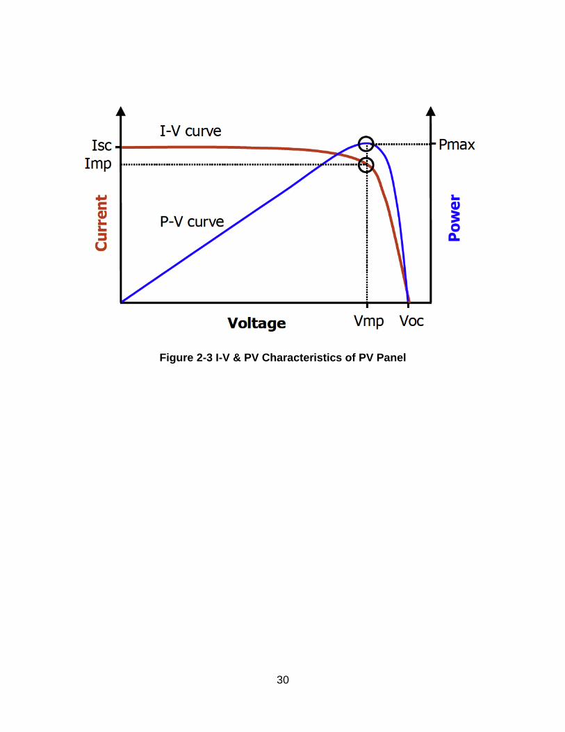
30
Figure 2-3 I-V & PV Characteristics of PV Panel

31
Figure 2-4 I-V Curves of Solar Panel with Varying Temperature and Irradiance Level

32
Figure 2-5 P-V Curves of Solar Panel with Varying Temperature and Irradiance Level

33
2.1.1 Observations from Solar Panel’s I-V and P-V Curves:
VMPP (Maximum Power Point Voltage) variation due to change in irradiance levels
is very small.
VMPP varies inversely with temperature (negative temperature coefficient).
Increase in temperature reduces VMPP which in turn reduces maximum power
available.
One key conclusion that can be arrived at from the above observations is that under
standard test conditions i.e. 25⁰C, VMPP is nearly constant. This unique feature of PV
panel enables to maintain the gain of Front End DC-DC Converter fairly constant at
room temperature. This constant gain requirement for PV panels helps in optimal design
of the Front End DC-DC Converter. The DC-DC Converter can be designed such that
its highest efficiency gain point intersects with the gain requirement for the PV panel at
Standard Test Conditions.
2.2 Full Bridge LLC Resonant Converter:
LLC Converter is a resonant converter topology. Like any other resonant converters,
LLC Converter has three key blocks in its topology as shown in figure 2-6[2.4].
1. Switching Network:
Switching network chops the input voltage or current into symmetric (in time
domain) high frequency square pulse and applies it across the resonant network.
Depending upon the gain requirement, the switching network may be half-bridge
or full bridge switching network.
34
2. Resonant Network:
Resonant network consists of a series and or parallel combination of Inductor
and Capacitor depending upon type of resonant converter. The energy applied
across the resonant tank by the switching network is circulated in the tank
network and some of it is delivered to the output either in the same or the next
switching cycle.
3. Rectifier Network:
Output of resonant tank is either stepped up or stepped down depending upon
the need of conversion ratio and applied across the Rectifier Network. The
rectifier network rectifies the high frequency AC and converts into the DC. For
converters with higher load current, the diode rectifier network can be replaced
by synchronous rectifier to reduce the conduction losses in rectifier diodes.
Figure 2-6 Block Diagram of Resonant Converter Topology
LLC Resonant converter is a series-parallel type resonant converter. The series
resonant tank consists of a series combination of Lr and Cr. This series network is in

35
parallel with Lm which forms the parallel tank circuit. Figure 2-7 illustrates a Full Bridge
LLC Resonant Converter. Parallel Inductor Lm is implemented as the magnetizing
inductance of the power transformer. This transformer is a step-up or step-down
depending upon the DC gain requirement.
Lr
S2
CrVin
S1
Lm
S3
S4
n:1
Vo
+
-
ir
im
D1 D2
D4D3
Figure 2-7 Full Bridge LLC Converter
2.2.1 LLC Converter FHA Analysis
Fundamental Harmonic Analysis [2.4] is widely used method to obtain DC gain curve for
LLC converter. This method simplifies the analysis by ignoring the higher order
harmonics of the square wave input voltage and treats the input purely sinusoidal.
Although this method is not very accurate but it greatly reduces the complexity of the
analysis. The transfer function of the LLC converter is obtained by applying FHA to AC
equivalent circuit of LLC Converter shown in figure 2-8. The resonant tank of LLC can
be divided into two impedances i.e. Series and Parallel.
Rectifier Network Switching Network Resonant Network

36
( 2.4 )
( 2.5 )
Lm
LrCr
Zs
Zp RacVin Vo(ac)Vin(ac)
Figure 2-8 AC Equivalent Circuit of LLC Converter
Figure 2-9 Derivation of AC Equivalent Impedance
Rac in the AC equivalent circuit shown above is the AC impedance of the output load
resistance reflected on the primary side of the transformer as shown in figure 2-9[2.4].

37
Assuming the output voltage Vo to be constant, the fundamental component of the
primary side voltage of the transformer can be calculated as
( 2.6 )
Assuming that the current at the input of the output rectifier network is sinusoidal in
nature, thereby output current Io is average of the sinusoidal current at the input of the
rectifier. Thus, the current at the primary side of the transformer can be calculated as
( 2.7 )
Thus, AC equivalent impedance can be calculated from (13) and (14) as
( 2.8 )
The normalized DC gain as a function of switching frequency as given in [2.6]:
( 2.9 )
Figure 2-10 plots the gain curves using equation (2.9) for different load values which is
reflected by Qe. Maximum achievable peak gain reduces with increase in load for a
fixed value of Lm, Lr and Cr. Also the frequency at which peak gain occurs is shifted
towards resonant switching frequency with increase in load.

38
Figure 2-10 LLC Converter Gain Curves (Ln=2)
LLC Converter has three characteristic frequencies:
1. Resonant Frequency (fo): This frequency is the function of Series tank
components. At this frequency, Zs is purely resistive and thus no circulating
power in the tank circuit..
( 2.10 )
2. Pole Frequency (fp): This frequency is the function of all the resonant parameters
of the tank circuit.
( 2.11 )
3. Peak Gain Frequency (fco): DC gain of the LLC converter is at its maximum at
this frequency. fco is load dependent; fp≤fco≤fo. At no load, fco=fp; when output is
short-circuited, fco=fo.
fo
fco
fp
Load Increases

39
In order to maintain control loop stability and to achieve Turn ON ZVS for the switches,
it is essential that switching frequency (fsw)>fco.
Depending upon the switching frequency (fsw), the LLC converter has three major
operating zones [2.5].
2.2.2 Operating Modes of LLC Converter
Zone 1- fco ≤ fsw≤ fo:
Figure 2-11 describe the waveforms of LLC Converter while operating in Zone 1. The
operation of the LLC converter in Zone 1 can be divided into 6 modes. Equivalent
circuits for each mode are shown in figure 2-12. For the sake of simplicity, parasitic
capacitances for the MOSFETs are not shown.
Mode 1(t0-t1):
At t=t0, S2 and S4 turns OFF. t0-t1 is the dead-time period, hence S1 and S3 are also
OFF. During this mode, the lagging current ir freewheels through body diodes of S1 and
S3. Since Lm is clamped by reflected output voltage, the resonance occurs in Lr and Cr
only.
Mode 2 (t1-t2):
At t=t2, S1 and S3 are turned ON at zero voltages across them due to freewheeling of ir
through their respective bypass diodes in Mode 1. The resonant current ir continues to
drop to zero and reverses its direction. The magnetizing current im, increases linearly
from negative peak to positive peak during this mode. The difference between resonant

40
current ir and magnetizing current im flows through output rectifier diodes D1 and D3
during this mode.
Mode 3 (t2-t3):
During this mode, Lr, Cr and Lm enter into resonance. Since Lm+Lr>Lr, the resonant
period of this resonance is longer than the switching period, thereby, ir and im can be
regarded as constant during this mode. As ir=im, there is no net current flowing into the
transformer, thereby, causing the diode D1 and D3 to turn OFF. Thus in this zone,
diodes are Zero Current Switched.
Since duty cycle of the switching network is 50%, operation in Mode 4, Mode 5 and
Mode 6 is similar as in Mode 1, Mode 2 and Mode 3 respectively. The waveforms in
these three modes are symmetrical with waveforms in Mode 1, Mode 2 and Mode 3.

41
Figure 2-11 Waveforms for Zone 1- fco≤fsw≤fo

42
Lr
S2
CrVin
S1
Lm
S3
S4
n:1
Vo
+
-
ir
im
D1 D2
D4D3
Lr
S2
CrVin
S1
Lm
S3
S4
n:1
Vo
+
-
ir
im
D1 D2
D4D3
Lr
S2
CrVin
S1
Lm
S3
S4
n:1
Vo
+
-
ir
im
D1 D2
D4D3
Lr
S2
CrVin
S1
Lm
S3
S4
n:1
Vo
+
-
ir
im
D1 D2
D4D3
Lr
S2
CrVin
S1
Lm
S3
S4
n:1
Vo
+
-
ir
im
D1 D2
D4D3
Lr
S2
CrVin
S1
Lm
S3
S4
n:1
Vo
+
-
ir
im
D1 D2
D4D3
Mode 1 – t0-t1 Mode 2 – t1-t2
Mode 3 – t2-t3 Mode 4 – t3-t4
Mode 5 – t4-t5 Mode 6 – t5-t6
Figure 2-12 Equivalent Circuits of Operation Modes of LLC Converter in Zone 1 - fco≤fsw≤fo

43
Zone 2- fsw=fo:
LLC converter enters this zone when the switching frequency of the switching network is
exactly same as resonance frequency. In this zone, there is only one resonance
occurring in Lr and Cr. Operation modes in this zone is similar to zone 1 except, there is
no Mode 3 and Mode 6. Figure 2-13 shows the waveforms during this zone. The gain in
this zone is unity, hence the only voltage conversion ratio available in this zone is
provided by the turns-ratio of the transformer. This is the most efficient operating point
of the LLC converter because of two reasons:
1. During the entire switching cycle, Lr and Cr are in resonance thereby, no
circulating current and hence no conduction losses in the tank circuit.
2. Due to resonance, the current is sinusoidal in nature. Due to sinusoidal nature of
the current, the RMS value of the operation current is low thereby less losses.
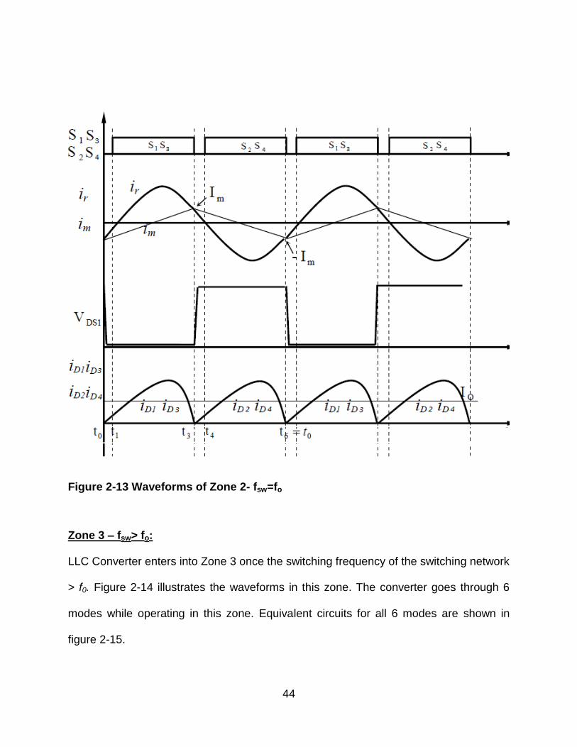
44
Figure 2-13 Waveforms of Zone 2- fsw=fo
Zone 3 – fsw> fo:
LLC Converter enters into Zone 3 once the switching frequency of the switching network
> f0. Figure 2-14 illustrates the waveforms in this zone. The converter goes through 6
modes while operating in this zone. Equivalent circuits for all 6 modes are shown in
figure 2-15.

45
Mode 1- (t0-t1):
At t=t0, S1 and S3 are turned ON. At the start of this mode, ir and im are equal. The input
voltage applied across the resonant network; causes Lr and Cr to undergo resonance.
Due to resonance, ir starts increasing sinusoidally. Since Lm does not undergo
resonance, ir and im begin to diverge. Difference between ir and im causes D1 and D3 to
go into conduction and is delivered to the load. Turning ON of D1 and D3 clamps Lm to
reflected output voltage. This clamped voltage causes the current im to linearly increase
from its negative peak to positive peak.
Mode 2 (t1-t2):
At t=t1, S1 and S3 are turned OFF. This is the dead-time period of the switching cycle.
Since S1 and S3 are turned OFF before the end of resonance period, ir >im. This
difference in the resonant and magnetizing currents keeps D1 and D3 conducting. Thus,
the reflected output voltage clamped across Lm and no input voltage, blocks the
resonant current ir and causes it reduce further rapidly. At the same time, the clamped
voltage across Lm keeps increasing im linearly.
Mode 3 (t2-t3):
At t=t2, S2 and S4 are turned ON which cause the resonant current ir to further drop. D1
and D3 are still conducting, which causes the Lm to be clamped at the reflected output
voltage. This clamped voltage also adds to the decay of ir and cause im to linearly
increase. This mode ends at t=t3, at which ir=im causing diodes D1 and D3 to turn OFF.

46
Since the switching network is switched at 50% duty cycle, Mode 4, Mode 5 and Mode 6
are similar to Mode 1, Mode 2 and Mode 3 respectively. The waveforms during Mode 4,
Mode 5 and Mode 6 are symmetrical to that of Mode 1, Mode 2 and Mode 3
respectively.
Figure 2-14 Waveforms of Zone 3 – fsw>fo

47
Lr
S2
CrVin
S1
Lm
S3
S4
n:1
Vo
+
-
ir
im
D1 D2
D4D3
Lr
S2
CrVin
S1
Lm
S3
S4
n:1
Vo
+
-
ir
im
D1 D2
D4D3
Lr
S2
CrVin
S1
Lm
S3
S4
n:1
Vo
+
-
ir
im
D1 D2
D4D3
Lr
S2
CrVin
S1
Lm
S3
S4
n:1
Vo
+
-
ir
im
D1 D2
D4D3
Lr
S2
CrVin
S1
Lm
S3
S4
n:1
Vo
+
-
ir
im
D1 D2
D4D3
Lr
S2
CrVin
S1
Lm
S3
S4
n:1
Vo
+
-
ir
im
D1 D2
D4D3
Mode 1 – t0-t1 Mode 2 – t1-t2
Mode 3 – t2-t3 Mode 4 – t3-t4
Mode 5 – t4-t5 Mode 5 – t5-t6
Figure 2-15 Equivalent Circuits of Operation Modes of LLC Converter in Zone 3 - fsw>fo

48
2.2.3 Discussion on Design considerations of LLC Converter as front end DC-DC Converter of Micro-Inverter
Front End DC-DC Converter of a micro-inverter has two primary functions.
1. Boost Converter: A typical 200W PV Panel delivers power at DC voltage level of
25-38V. This voltage level is not enough to invert the power at line voltage levels.
Hence, there is a need to boost the DC voltage output of the PV Panel.
2. MPPT Controller: As seen in figure 2-13, a PV panel has an optimal operating
point at which it delivers maximum power. This operating point varies with
temperature and irradiance levels. Front End converter needs to make sure that
the power is extracted from the PV panel at this maximum power point.
LLC topology is a highly suitable candidate to be used as front end DC-DC converter for
micro-inverter for following reasons [2.7-2.9]:
1. Wide input voltage range.
2. High gain range.
3. Low component count.
4. Soft-Switching capability.
Apart from the advantages mentioned above, LLC converter has a unique feature which
complements well with certain features of the PV panel.
As explained in operating modes of LLC resonant converter, the highest operating
efficiency is obtained in Zone 2 i.e. fsw = fo. Also in this zone, the voltage gain is
independent of load. As mentioned in section 2.1.1, at a constant temperature the

49
variance is VMPP with respect to irradiance levels is very low. Hence, LLC Converter can
be designed such that it operates in zone 2 when PV panel is operating at room
temperature. As the voltage gain in zone 2 is independent of load and in case of PV
panel as the input source, voltage gain is independent of irradiance levels; the LLC
converter operates at its highest efficiency point for entire load range. As show in figure
2-16, zone 2 of LLC converter coincides with Maximum Power Point of PV Panel at
room temperature.
Figure 2-16 Optimal Design Consideration for LLC Converter as front DC-DC converter of Micro-Inverter

50
2.3 Design Procedure for Resonant Parameters of LLC Converter as Front End DC-DC Converter of Micro-inverter
This section provides the design procedure for calculating resonant parameters for LLC
converter. In order to design the LLC converter first the design specifications needs to
be derived with the help of PV Panel Datasheet.
2.3.1 Deriving the Design Specifications
In this design example, the input PV panel is 410W PV panel from Advanced Solar
Photonics and the rectifier network is a voltage doubler.
Desired output voltage = 400V.
Maximum output power = 400W.
1. Turns Ratio:
In order to operate LLC Converter at highest efficiency point at room
temperature, the LLC converter should operate in zone 2. In this operation zone,
the gain of the LLC converter is unity. Hence the required gain to boost PV panel
voltage to 400V should be achieved from the turns-ratio of the transformer.
( 2.12 )
2. Gain Range:
Gain range can be calculated from the operating temperature range of the micro-
inverter. PV Panel VMPP has a negative temperature coefficient i.e. VMPP
decreases with increase in temperature.
( 2.13 )

51
( 2.14 )
2.3.2 Calculating Resonant Parameters
Once the turns ration and gain range is obtained, the resonant parameters i.e. Lr, Cr
and Lm are calculated using procedure shown in [2.6]
DC gain curve of LLC converter is a function of two dummy variables i.e. Ln and Qe as
defined by equation (2.9) respectively. Behavior of DC gain with variance in Ln and Qe
can be summarized as follows:
1. As shown in figure 2-10, the gain reduces with increase in Qe i.e. gain reduces
with increase in load current.
2. Lower Qe increases the maximum achievable gain but the associated gain
curves require large frequency variation for a given gain adjustment.
3. For a fixed value of Qe, maximum achievable gain varies inversely with Ln. This
phenomenon can be observed in figure 2-17. However, lower value of Ln cause
Lm to reduce which in turn increases the magnetizing current. Increase in
magnetizing current leads to increase in circulating current, thereby increasing
the losses.
4. From figure 2-17, it can also be concluded that a particular value of gain can be
achieved by more than one combination of Ln and Qe values.
5. It can be seen from figure 2-18 that for a fixed Qe (load current), increase in Ln
leads to an increase in frequency variation for a given gain adjustment.

52
As the required gain can be achieved using different combinations of Ln and Qe, Ln =5
and Qe=0.5 is considered to be a good starting point [2.6]. From this starting point,
further reiteration is necessary to achieve an optimal combination of Ln and Qe such
that required gain is obtained with minimum losses.
Figure 2-17 Normalized Gain, M vs Quality Factor, Qe

53
Figure 2-18 Gain vs Switching Frequency-Fixed Qe-Variable Ln
Once the values of Ln and Qe are obtained, resonant parameters can be calculated
using following equations.
( 2.15 )
( 2.16 )
( 2.17 )

54
2.3.3 Design Example
This design example considers a 410W mono-crystalline PV panel from Advanced Solar
Photonics at the input of a full bridge LLC Converter with voltage doubler as the output
rectifier network as shown in figure 2-19
Lr
S2
Cr
S1
Lm
S3
S4
n:1
ir
im
D1
D2
C1
C2
DC-AC Inverter
DC-AC Inverter GRIDGRID
Figure 2-19 Full Bridge LLC Converter as Front End DC-DC Converter for Micro-Inverter
The above mentioned PV Panel has following specifications at standard test conditions:
Pmax =410W
VMPP= 50.34V.
IMPP=8.15A.
Temperature Coefficients:
o Power (%/°C) = -0.49.
o VMPP (%/°C) = -0.40.
Input specifications for a temperature range of -40°C to 65°C can be derived as:

55
In the above equation output voltage is divided by 2 to compensate the voltage gain
provided by voltage-doubler.
Based on the calculation method described in previous section, after certain design
iterations; following are the final resonant parameters.
Gain curve for the above design is shown in figure 2-20. From the figure it can be seen
that the design is able to meet Mmax requirement, however, it does not meet Mmin
requirements at maximum frequency. In order to achieve the Mmin requirement, the
converter must be operated in half bridge mode at higher input voltages i.e. at lower
temperatures.
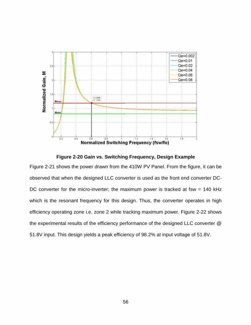
56
Figure 2-20 Gain vs. Switching Frequency, Design Example
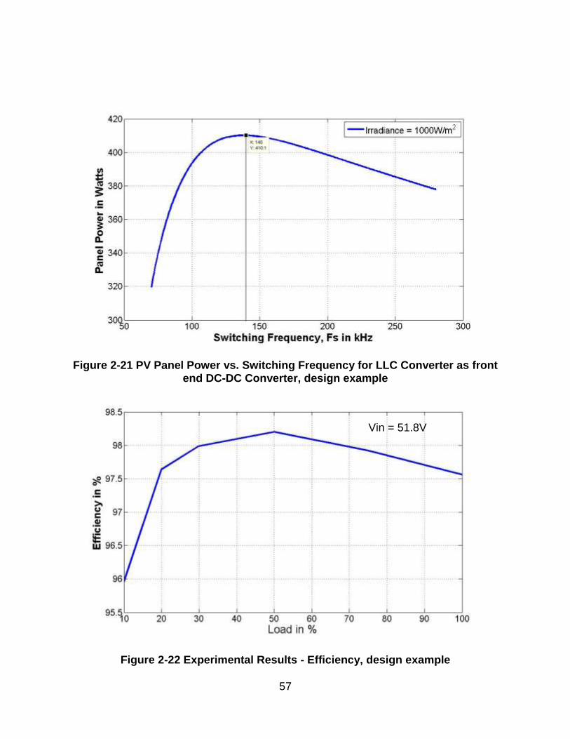
Figure 2-21 shows the power drawn from the 410W PV Panel. From the figure, it can be
observed that when the designed LLC converter is used as the front end converter DC-
DC converter for the micro-inverter; the maximum power is tracked at fsw = 140 kHz
which is the resonant frequency for this design. Thus, the converter operates in high
efficiency operating zone i.e. zone 2 while tracking maximum power. Figure 2-22 shows
the experimental results of the efficiency performance of the designed LLC converter @
51.8V input. This design yields a peak efficiency of 98.2% at input voltage of 51.8V.
57
Figure 2-21 PV Panel Power vs. Switching Frequency for LLC Converter as front end DC-DC Converter, design example
Figure 2-22 Experimental Results - Efficiency, design example
Vin = 51.8V

58
2.4 References
2.1 Bellini, A.; Bifaretti, S.; Iacovone, V.; Cornaro, C., "Simplified model of a
photovoltaic module," Applied Electronics, 2009. AE 2009 , vol., no.,
pp.47,51, 9-10 Sept. 2009
2.2 Solmetric. Guide to Interpreting I-V Curve Measurements of PV Arrays –
Application Note PVA-600-1.
2.3 Florida Solar Energy Centre (2002), Photovoltaic Modules and Arrays. Retrieved
from
http://www.pttrenenergy.upc.edu/index2.php?option=com_docman&task=doc_vi
ew&gid=213&Itemid=35
2.4 Fang, X. (2012).Analysis and Design Optimization of Resonant DC-DC
Converters (Doctoral Dissertation). Retrieved from UCF Libraries Database.
2.5 Huang, Guisong; Gu, Yilei (2000), Delta Power Electronics Center. Half Bridge
LLC Converter (Technical Report).
2.6 Huang, Hong ;. Designing an LLC Converter Half-Bridge Power Converter Texas
Instruments Design Application Note.
2.7 Jee-Hoon Jung; Joong-Gi Kwon, "Theoretical analysis and optimal design of
LLC resonant converter," Power Electronics and Applications, 2007 European
Conference on , vol., no., pp.1,10, 2-5 Sept. 2007.
2.8 Chun-An Cheng; Hung-Wen Chen; En-Chih Chang; Chun-Hsien Yen;
Kun-Jheng Lin, "Efficiency study for a 150W LLC resonant

59
converter," Power Electronics and Drive Systems, 2009. PEDS 2009.
International Conference on , vol., no., pp.1261,1265, 2-5 Nov. 2009
2.9 Pawellek, A.; Oeder, C.; Duerbaum, T., "Comparison of resonant LLC
and LCC converters for low-profile applications," Power Electronics and
Applications (EPE 2011), Proceedings of the 2011-14th European
Conference on , vol., no., pp.1,10, Aug. 30 2011-Sept. 1 2011.

60
CHAPTER 3: LIGHT LOAD EFFICIENCY IMPROVEMENT OF THREE PHASE GRID TIED INVERTERS
3.1 Daily Solar Irradiance Pattern
Incident solar power on a PV panel is function of time of day, time of year, shading,
cloud cover and the location co-ordinates. On a typical day in a non-polar region, with
clear sky and no partial shading, the incident power reaches its maximum during the
day at noon and its minimum at night. The solar irradiance profile on a typical day
appears like a Gaussian curve as shown in figure 3-1 below.
Figure 3-1 Solar Irradiance Pattern on a Typical Day
The N point Gaussian curve can be represented in a discrete form using the following
equation from [3.1]:

61
( 3.1 )
( 3.2 )
The width of Gaussian curve is inversely proportional to α. Thus, for solar irradiance
pattern α is an indirect function of length of day i.e. the time between sunrise and
sunset. During summer time, the length of day is longer than the length of day during
winter, thereby the irradiance curve during summer time are wider than the ones during
winter.
NREL’s Solar Radiation Research Laboratory located at Golden, Colorado, US
continuously measures solar radiation components. From their measured solar
irradiance pattern shown in figure 3-2 it can be verified that on a typical day the solar
irradiance pattern follows a Gaussian curve. The figure 3-2 below shows irradiance
pattern of a typical day during summer time and winter time. It can be concluded by
observation that during summer time when the length of day is longer, the width of
irradiance curve is wider. Figure 3-3 shows irradiance patterns of a cloudy day. From
the irradiance curves of cloudy days, it can be deduced that, the available solar power is
at its peak for less than 10% of the day time.
Due to highly variable nature of available solar power, it is essential for a PV inverter to
have flat efficiency response over its entire load range. In order to have more realistic
efficiency index, PV inverters are evaluated according to their weighted efficiency and
not at peak efficiency.

62
Figure 3-2 Solar Irradiance Patterns – Clear Days

63
Figure 3-3 Solar Irradiance Curves – Cloudy Days

64
3.2 Significance of Weighted Efficiency for PV Inverters
In the previous section, it was established the available solar power is highly variable
and function of myriad of parameters like
1. Length of Day.
2. Time of the Day.
3. Time of the Year.
4. Location Co-ordinates
5. Cloud Cover.
6. Partial Shading due to leaves.
7. Dust.
Based on the solar irradiance measurements done by NREL which are shown in Figure
3-2 and 3-3, it can be concluded that PV inverter is required to operate over its entire
load curve for fair share of time. In order to justify the high investment cost required in
PV as compared to conventional sources of energy, it is of utmost importance to extract
every single watt of power at the best possible conversion efficiency.
Typically, every power converter has an optimal operating load point at which the
converter’s power conversion efficiency peaks. At other load points, the conversion
efficiency deteriorates for the reasons explained in the next section of this chapter. If a
converter is required to operate at a fixed load, then it can be designed such that the
peak conversion efficiency load point of the converter intersects with the fixed operating
load point at which converter is specified to operate. However, for PV applications, as

65
the available power to be converted is constantly varying, the Power Converters for PV
applications are evaluated at Weighted Efficiency rather than peak efficiency. Weighted
efficiency is a performance index which is widely used in PV applications as it generates
the efficiency index based on the efficiency performance of the inverter over its entire
load range.
Depending upon the geography, two sets of weighted efficiency performance indices
are available [3.2]. These two efficiency indices vary in terms of weights assigned to
different load points.
1. European Weighted Efficiency.
( 3.3 )
2. California Energy Commission Weighted Efficiency (US).
( 3.4 )
In order to achieve a higher weighted efficiency for Three Phase Inverters for Grid Tied
PV applications, a control technique, Phase Skipping Control is proposed to improve the
light load efficiency performance of the inverter. This control technique has been
implemented for Three Phase Half Bridge PWM Inverter; however, it can be easily
extended to any class of Three Phase Inverters.

66
3.3 Efficiency Behavior in Power Converters
Typically every power converter has an optimal operating point at which its efficiency
peaks. Figure 3-4 shows the efficiency curve of such a typical power converter.
Efficiency is low at light loads, it recovers with increase in load and reaches its
maximum at around 70%-80% of its full load capacity and droops slightly at full load.
Figure 3-4 Efficiency Curve of a Typical Power Converter
Losses in a power converter are composed of two factors which causes the above
mentioned efficiency curve of power converters [3.3].
( 3.5 )

67
1. Load Dependent Losses: These are losses in power converters which are
dependent on the load like conduction losses in switches, copper losses in
magnetics.
2. Load Independent Losses: These losses are not a function of load current.
They are a function of supply voltages, switching frequency and ripple current
through the magnetics. These losses are switching losses, magnetic core losses,
high frequency AC copper losses magnetics due to high frequency ripple current
and diode recovery losses.
Efficiency of a power converter can be represented by following equation:
( 3.6 )
Combining equation (*#*) and (*#*) together and expressing them as a function of load
current we get:
( 3.7 )
As PLoad Independent Loss is not a function of load current, at lighter loads it dominates the
losses as well as tends to keep the numerator constant in equation (3.7). As
denominator comprises of Pin which is a function of load current, it becomes smaller at
lighter loads, thereby, deteriorating the efficiency at lighter loads. At heavier loads, the
conduction loss tends to dominate the total losses. As conduction losses are mostly I2R
losses, they are a square law function of load current whereas Pin is a linear function of
load current. This causes the efficiency to slightly droop at higher loads. The variation in
losses with load current and its impact on efficiency is qualitatively represented in figure
3-5.

68
Figure 3-5 Impact of Losses on Efficiency as a Function of Load Current
In order to achieve a better weighted efficiency, the inverter must have a flat efficiency
response over its entire load range. Various methods like variable switching frequency
control, phase shedding, burst mode operation, using energy storage, bulk voltage
reduction have been proposed in the literature for DC-DC Converters[3.3 – 3.9]. In order
to improve light load efficiency for inverters, techniques like “Pulse Skipping” and
different modulation techniques are proposed in the literature [3.10-3.12, 3.15]. Pulse
Skipping causes the inverter to operate in burst mode which tends to create instability
into the grid. Modulation Technique proposed in [3.10] [3.11] are topology specific.

69
Phase Skipping Control is a topology independent control technique which improves the
light load efficiency for multiphase inverters. In order to establish a proof of concept, this
technique has been implemented on a Half Bridge Three Phase PWM Inverter and
analysis for this topology is given.
3.4 Half Bridge PWM Inverter
Half Bridge PWM Inverter is essentially a Sinusoidally Modulated Synchronous Buck
Converter with a bipolar bus voltage. Figure 3-6 illustrates the topologies of
Synchronous Buck Converter and Half Bridge Inverter.
C
S1
S2
VdL1
C1
L2
RLC2
C1S1
S2
Vd
C2
L1
C1
L2
RLC2
Synchronous Buck
ConverterHalf Bridge Inverter
Figure 3-6 Comparison of Synchronous Buck Converter and Half Bridge Inverter
The gate drive signals for the MOSFET’s of Half Bridge PWM Inverter are generated by
modulating Saw Tooth Carrier Signal with Sinusoidal Reference. Frequency of carrier
signal defines the switching frequency of the inverter and frequency of the modulating
sinusoidal signal controls the frequency of the output voltage. Figure 3-7 illustrates the

70
gate drive signals for the Half Bridge Inverter. The Top Side MOSFET and Bottom Side
MOSFET signals are complementary PWM Signals with dead-time (td) between them to
avoid cross conduction of the two switches.
Figure 3-7 Gate Drive Signal for Half Bridge Inverter
Output voltage of the Half Bridge Inverter is a function of the modulation index (m). The
modulation index is calculated as:
( 3.8 )
For a proper sinusoidal output voltage, the modulation index m is less than unity. If m
exceeds more than unity, then it leads to clipping of the output voltage.

71
3.4.1 Half Bridge Inverter Operation:
The operation of Half Bridge Inverter is divided into eight operation modes, four for each
half cycle of the line voltage. Figure 3-8 illustrates all eight operation modes using the
topology diagrams. Figure 3-9 and Figure 3-10 describe the operation mode waveforms
of positive and negative half cycle respectively.
Mode 1(t0-t1):
This mode occurs during the positive line half cycle. Top side MOSFET S1 is turned ON
while bottom side MOSFET S2 is turned OFF at t0. In this mode, MOSFET S1 is hard
switched while turning ON. Due to hard switch turn ON, discharge of Drain to Source
Capacitor of S1 and reverse recovery of body diode of S2, there is a current spike at the
start of this mode. VGS(S1) exhibits a plateau region which occurs because of increase
in Coss(S1) caused due to collapse of drain to source voltage. Once the MOSFET is
completely turned ON, the VDS (S1) drops to IL2RDS(ON) voltage drop across S1. Current
through inductor (L1) rises linearly with the slope given by:
( 3.9 )
The inductor current continues to rise with the slope given in (4.9) until t1 where this
mode ends.
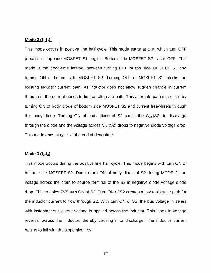
72
Mode 2 (t1-t2):
This mode occurs in positive line half cycle. This mode starts at t2 at which turn OFF
process of top side MOSFET S1 begins. Bottom side MOSFET S2 is still OFF. This
mode is the dead-time interval between turning OFF of top side MOSFET S1 and
turning ON of bottom side MOSFET S2. Turning OFF of MOSFET S1, blocks the
existing inductor current path. As inductor does not allow sudden change in current
through it; the current needs to find an alternate path. This alternate path is created by
turning ON of body diode of bottom side MOSFET S2 and current freewheels through
this body diode. Turning ON of body diode of S2 cause the CDS(S2) to discharge
through the diode and the voltage across VDS(S2) drops to negative diode voltage drop.
This mode ends at t2 i.e. at the end of dead-time.
Mode 3 (t2-t3):
This mode occurs during the positive line half cycle. This mode begins with turn ON of
bottom side MOSFET S2. Due to turn ON of body diode of S2 during MODE 2, the
voltage across the drain to source terminal of the S2 is negative diode voltage diode
drop. This enables ZVS turn ON of S2. Turn ON of S2 creates a low resistance path for
the inductor current to flow through S2. With turn ON of S2, the bus voltage in series
with instantaneous output voltage is applied across the inductor. This leads to voltage
reversal across the inductor, thereby causing it to discharge. The inductor current
begins to fall with the slope given by:

73
( 3.10 )
VGS(S2) does not exhibit an plateau region like top side MOSFET. This is because
before turn ON of S2, the VDS(S2) is already negative voltage drop. Turning ON of S2
makes the voltage across drain to source terminals less negative and clamps it to
IL2RDS(ON) drop. Thus, there is no large change in voltage thereby leading to no
significant change in Coss(S2).
This mode ends with start of turning OFF process of bottom side MOSFET S2 occurring
at t3.
Mode 4 (t3-t4):
This is the last mode occurring in positive line half cycle. This mode is exactly similar to
Mode 2. Start of turn OFF process of bottom side MOSFET S2 brings the inverter in this
mode. As the current through S2 begins to decrease, this causes the discharging
inductor current which is still positive to turn ON the body diode of S2 in the search of
alternate path to flow. Turning ON of body diode clamps the VDS(S2) to negative diode
drop voltage thus enabling ZVS Turn OFF of bottom side MOSFET.
During entire positive half cycle, the bottom side MOSFET is completely soft switched.

74
Mode 5 – Mode 8 (t5-t9):
Mode 5 – Mode 8 are similar to Mode 1- Mode 4. The only difference is that the all the
voltage and current transitions occurring on S1 and S2 which was explained in Mode 1-
Mode 4 is swapped i.e. S2 in Mode 5-Mode 8 behaves like S1behaves in Mode 1- Mode
4 and S1 in Mode 5-Mode 8 behaves like S2 behaves in Mode 1-Mode 4. Another
difference between these two sets of Modes is that direction if inductor current is
negative. Figure 3-10 illustrates the waveforms of Mode 5- Mode 8.
During Mode 5 and Mode 7 the inductor charges and discharges in the negative
direction with slopes given in (3.9) and (3.10) respectively. During Mode 6 and Mode 8,
the inductor current freewheels through top side MOSFET’s body diode.
During Mode 5 – Mode 8, top side switch is completely soft switched.

75
C1S1
S2
Vd1
C2
L1
C1
L2
RLC2
Mode 1: S1 – ON, S2-OFF
Positive Half Cycle C1S1
S2
C2
L1
C1
L2
RLC2
Mode 2: S1 – OFF, S2-OFF, Deadtime
Positive Half Cycle
Vd2
S1
S2
L1
C1
L2
RLC2
Mode 3: S1 – OFF, S2-ON
Positive Half Cycle
Vd2
Vd1
Vd1
Vd2
IL1 IL1
IL1
C1S1
S2
C2
L1
C1
L2
RLC2
Mode 4: S1 – OFF, S2-OFF, Deadtime
Positive Half Cycle
IL1
Vd1
Vd2
C1S1
S2
Vd1
C2
L1
C1
L2
RLC2
Mode 7: S1 – ON, S2-OFF
Negative Half Cycle
C1S1
S2
C2
L1
C1
L2
RLC2
Mode 6: S1 – OFF, S2-OFF, Deadtime
Negative Half Cycle
Vd2
S1
S2
L1
C1
L2
RLC2
Mode 5: S1 – OFF, S2-ON
Negative Half Cycle
Vd2
Vd1Vd1
Vd2
IL1
IL1IL1
Vd1
Vd2
C1S1
S2
C2
L1
C1
L2
RLC2
Mode 8: S1 – OFF, S2-OFF, Deadtime
Negative Half Cycle
IL1
Figure 3-8 Half Bridge Inverter - Operation Modes - Topology

76
Vgs(S1)
Vds(S2)
Vgs(S2)
Ids(S1)
Ids(DS2)
Mode 1 Mode 2 Mode 3 Mode 4
Vds(S2)
Free Wheeling Through
Body Diode
Free Wheeling Through
Body Diode
t0 t1 t2 t3 t4
Positive Half
Cycle
Gate To
Source
Voltage
Drain To
Source
Voltage
Drain To
Source
Current
Inductor
(L1)
Current
Figure 3-9 Half Bridge Inverter - Operation Mode Waveforms - Positive Half Cycle

77
Vgs(S2)
Vds(S1)
Vgs(S1)
Ids(S2) Ids(DS1)
Mode 5 Mode 6 Mode 7 Mode 8
Vds(S2)
Free Wheeling Through
Body Diode
Free Wheeling Through
Body Diode
t5 t6 t7 t8 t9
Negative Half
Cycle
Gate To
Source
Voltage
Drain To
Source
Voltage
Drain To
Source
Current
Inductor
(L1)
Current
Figure 3-10 Half Bridge Inverter - Operation Mode Waveforms- Negative Half Cycle

78
3.4.2 Loss Analysis of Half Bridge Inverter:
Following are the main losses occurring in a Half Bridge Inverter:
C1S1
S2
Vd1
C2
Vd2
L1
C1
L2
RLC2
RG(ON)
RG(OFF)
D1
RG(ON)
RG(OFF) D2
Vdriver
VG2
Rdriver
Vdriver
Rdriver
Figure 3-11 Half Bridge Inverter - With Drive Circuit
1. Losses in MOSFETs:
Losses in MOSFETs can be divided into two parts:
a. Switching Losses:
Switching Losses in MOSFETs are composed of 3 entities:
i. Cross Over Losses occurring due to hard switching of the MOSFET:
As one of the two MOSFET is completely soft switched, this loss occurs only
in one of the MOSFETS.

79
Figure 3-12 illustrates the VDS and ID waveforms during switching transitions
in the MOSFET. Looking at the waveform, the cross over losses can be
estimated by the following equation in [3.12-3.13]
( 3.11 )
( 3.12 )
( 3.13 )
( 3.14 )
( 3.15 )
( 3.16 )
VPL can be extracted from the datasheet of the MOSFET.

80
VGSVDS(OFF)
IDS(ON)
Vth
Vpl
T(ON)
QG
VGS
IDS(ON)
Vth
Vpl
T(OFF)
QG
VDS(OFF)
VDS(ON)
VDS(ON)
TURN
ON
TURN
OFF
Figure 3-12 MOSFET Switching Waveform
ii. Conduction Losses:
Conduction Losses occurring in both MOSFETs are I2RDS(ON) losses. These
losses can be estimated by:
( 3.17 )
( 3.18 )
b. Losses occurring due to discharge COSS:
This loss occurs due to charge stored in COSS of the MOSFETs. If both
MOSFETS are identical then losses occurring in both MOSFETs due to COSS
discharge can be estimated by the following equation [3.12-3.15]:

81
( 3.19 )
c. Recovery Losses of Body Diode:
One of the body diode turns ON during the dead-time period; turning OFF of
this body diode leads to reverse recovery losses. Figure 3-13 shows the
reverse recovery phenomenon during positive line half cycle. During positive
half cycle, bottom side MOSFET’s body diode turns ON during the dead-time.
The inverter is operating in MODE4 (refer to figure 3-8). During the transition
from MODE 4 to MODE1, the body diode of bottom side MOSFET is turned
OFF and it goes through reverse recovery.
Figure 3-13 Diode Reverse Recovery Waveforms

82
At any point in the line cycle, body diode of only one of the MOSFETs turns
ON. Thus, reverse recovery losses occur in the body diode of only one of the
MOSFETs. If both MOSFETs are identical then power loss occurring during
the reverse recovery phenomenon can be estimated by a common equation.
From figure 3-13 [3.13], it can be seen that reverse recovery phenomenon
occurs between t0-t2, however, the power loss occurs only between t1-t2 as
prior t1 the voltage across the body diode is equal to forward diode voltage
drop. Thus, recovery losses can be estimated by
( 3.20 )
2. Drive Losses:
Charging and discharging of input gate capacitance of the MOSFET’s causes
some dissipation of power across the resistances between the driver and the
gate of the MOSFET. This drive loss PDRIVER can be calculated as [3.14]:
( 3.21 )
3. Body Diode Conduction Loss:
Dead-time is introduced between the complementary gate drives to avoid cross
conduction between two switches. During this dead-time, depending upon the
half cycle, current is flowing through either of the MOSFET’s body diode
conducts. Dead-time losses can be estimated by [3.13]:
( 3.22 )

83
4. Losses in Magnetics:
Losses occurring in the filter inductor can be divided into 3 entities:
a. Line Frequency Copper Loss:
This is the line frequency conduction loss occurring in the filter inductor. This
loss can be estimated by:
( 3.23 )
b. Switching Frequency Copper Loss:
This is the switching frequency conduction loss occurring in the filter inductor.
This loss can be estimated by:
( 3.24 )
( 3.25 )
c. Line Frequency Core Losses:
This is the hysteresis loss occurring in the inductor at line frequency. This loss
can be estimated using Steinmetz Relationship as given below:
( 3.26 )
( 3.27 )
.

84
d. Switching Frequency Core Loss:
This is the hysteresis loss occurring in the inductor at switching frequency.
This loss can be estimated using Steinmetz Relationship as given below:
( 3.28 )
( 3.29 )
.
3.4.3 Loss Model of Half Bridge Inverter:
Based on the loss analysis in the previous, a loss model for Half Bridge Inverter can be
created. This loss model will consist of two entities:
( 3.30 )
1. Load Independent Losses:
Load Independent losses comprises of the losses which are not a function of
load current. The losses which fall under this category are:
a. Diode Recovery Losses –PReverse Recovery Loss.
b. COSS Discharge Losses PCoss Loss.
c. Drive Losses PDRIVE LOSS.
d. Switching Frequency Copper Loss PSwitching Freq Copper Loss.

85
e. Switching Frequency Core Loss PSwitching Freq Core Loss.
( 3.31 )
Substituting equations (3.19), (3.20), (3.21), (3.24), (3.28) in equation (3.31) we
get :
( 3.32 )
2. Load Dependent Losses:
Load dependent losses are a function of load current. These losses vary with
load current. Following losses fall under this category:
a. Cross Over Switching Loss PCross over Switching Loss.
b. Switch Conduction Losses P Switch Conduction Loss
c. Body Diode Conduction Losses PBody Diode Conduction Loss.
d. Line Frequency Core Loss PLine Freq Core Loss.
e. Line Frequency Copper Loss PLine Freq Copper Loss.
( 3.33 )
Substituting equations (3.11), (3.17), (3.22), (3.23), (3.26) in equation (3.33) we get
( 3.34 )
From equation (3.33) and (3.34) we can get a total loss equation as follows:

86
( 3.35 )
Where
.
.

87
3.4.4 Verification of Loss Model
The above mentioned loss model was applied to a single phase half bridge inverter with
following specifications:
1. Input DC Voltage = 400V.
2. Maximum Power = 130W.
3. Output AC Voltage = 110V (rms).
4. fsw=20kHz.
Following circuit components were used:
1. S1,S2 – FCB20N60F
2. L1= 3.6mH, RAC(60Hz) =0.273Ω, RAC(20kHz)=12.4Ω.
3. L1 Core type – Ferrox Cube 42/29 Pot Core, Core Material – PC95.
4. L2=470μF, RAC(60Hz) = 80mΩ.
5. C1=C2=1μF.
6. Driver IC – HCPL-3180-360E, VDRIVER =12V, RG(ON) = 22Ω, RG(OFF) =0.05Ω.
7. Dead-time = 800nS.
8. Modulation Index = 0.83.
9. IRIPPLE(RMS) =300mA, IRIPPLE(PEAK)=0.65A.
Figure 3-14 and 3-15 shows the load independent and load dependent losses
respectively based on application of the proposed loss model to the above mentioned
single phase half bridge inverter. Figure 3-17 shows the calculated efficiency single
phase half bridge inverter with the above mentioned specifications; obtained from the
loss model. In order to verify the accuracy of the model, the calculated results are

88
compared with the experimental efficiency measurements. From figure 3-17, it can be
concluded that loss model calculations closely follow the experimental results and
thereby the loss model can be deemed accurate. In this loss analysis and efficiency
measurement, drive losses are not accounted for.
Figure 3-14 Load Independent Losses based on Loss Model, design example

89
Figure 3-15 Load Dependent Losses based on Loss Model, design example.
Figure 3-16 Losses in Half Bridge Inverter, design example
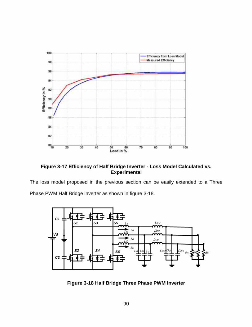
90
Figure 3-17 Efficiency of Half Bridge Inverter - Loss Model Calculated vs. Experimental
The loss model proposed in the previous section can be easily extended to a Three
Phase PWM Half Bridge inverter as shown in figure 3-18.
ia
C1S1
S2
S3
S4
S5
S6
Vd
C2
La
Lb
Lc
CbCa Cc
ib
ic
Lao
Lbo
Lco
Ra Rb RcCbo CcoCao
Figure 3-18 Half Bridge Three Phase PWM Inverter

91
3.5 Phase Skipping Control of Three Phase Micro-Inverter
In the previous section, it was proved using theoretical calculations as well as
experimental results that efficiency of a Half Bridge Three Phase PWM Inverter drops
dramatically at lighter loads. This dramatic drop in the efficiency at lighter loads is
caused because of the load independent losses in the inverter. In order to improve the
light load efficiency of Grid Tied Three Phase Micro-inverter, Phase Skipping Control
Technique is proposed.
3.5.1 Concept
Phase Skipping Control technique employs selective injection of power through
individual phases depending upon the power available from the PV panel. The micro-
controller continuously monitors the power being injected into the grid. Once the power
falls below a predetermined threshold, in this case it is 30% of the total power capacity;
the micro-controller shuts down two out of three phases. This shutting down of two
phases diverts the power from other two phases onto a single phase which now
operates at up to 90% instead of 30% of its per phase load capacity. Thus, now the
entire available power is converted using only single phase which is operating at up to
90% of its per phase capacity and thereby at efficiency corresponding to up to 90%
load. This mode of operation is called Phase Skipping. Figure 3-19 describes
conceptual operation of Phase Skipping. As Grid-Tied Inverters do not have a dedicated
load to drive them, selective phase power injection can be applied to them.

92
Figure 3-19 Conceptual Diagram - Normal Mode - Phase Skipping Mode

93
3.5.2 Implementation of Phase Skipping Control for Three Phase Grid Tied Micro-Inverters
In order to implement the phase skipping control, available input power from the front
end MPPT controller is constantly monitored. Once the available power drops below a
predefined power level PPHASE SKIPPING i.e. 30% Load, the on board controller disables
the PWM drive to 2 out of 3 phases.
Figure 3-20 shows the implementation scheme for Phase Skipping Control, it can be
seen from the figure, that the digital micro-controller constantly monitors the available
input power from the MPPT controller. Depending upon the available input power, the
micro-controller drives all the 3 phases when available power is greater than 30% of
PMAX i.e. Normal Mode of operation or just 1 phase when the available power is less
than 30% of PMAX. Figure 3-21 shows the flowchart of the software implementation of
Phase Skipping Control Scheme.
Phase Skipping Mode can also be implemented in two stages. Inverter enters into
Stage 1 of operation when input power is less than 66% of PMAX. During Stage 1, power
is injected through 2 out of 3 phases and thereby disabling only 1 out of 3 phases.
When the available power further drops less than 30% of the PMAX, the inverter enters
into Stage 2 of operation. During Stage 2, power is injected using just one phase.
Efficiency curve of the inverter under consideration determines whether the phase
skipping mode is implemented in one stage or two stages. If the efficiency of the
inverter starts dropping significantly after 65% load than two stage implementation of

94
phase skipping mode can be justified. However, if the efficiency drop up to 30% load is
not significant enough then the phase skipping mode is implemented using single stage.
Figure 3-20 Implementation of Phase Skipping Control Scheme- Singe Stage
Figure 3-21 Flow Chart of Phase Skipping Control Algorithm-Single Stage

95
3.5.3 Experimental Results of Phase Skipping Control
Phase Skipping Control is a generic control technique independent of the topology. In
order to establish the proof of concept, this control technique was implemented on a
DC-AC stage of the prototype as shown in figure 3-22. DC-AC stage is implemented
using a Three Phase Half Bridge Inverter with following specifications:
1. Input DC Voltage = 400V.
2. Maximum Output Power = 400W.
3. Output AC Voltage = 110V (rms).
4. fsw=20kHz.
Following circuit components were used:
1. S1, S2, S3, S4, S5, S6 – FCB20N60F
2. La=Lb=Lc= 3.6mH, RAC(60Hz) =0.273Ω, RAC(20kHz)=12.4Ω.
3. La=Lb=Lc Core type – Ferrox Cube 42/29 Pot Core, Core Material – PC95.
4. Lao=Lbo=Lco=470μF, RAC(60Hz) = 80mΩ.
5. Ca=Cb =Cc=Cao=Cbo=Cco=1μF.
6. Driver IC – HCPL-3180-360E, VDRIVER =12V, RG(ON) = 22Ω, RG(OFF)=0.05Ω.
7. Dead-time = 800nS.
8. Modulation Index = 0.83.
9. IRIPPLE(RMS) /phase=300mA, IRIPPLE(PEAK) /phase=0.65A.
The schematic of the prototype is shown in figure3-23.

96
Figure 3-22 Prototype of 400W Three Phase Micro-Inverter
The prototype develop has a front end LLC DC-DC converter. This front-end converter
is designed as per the design guidelines in chapter 2. Output of the front-end DC-DC
stage is fed to Three Phase Half Bridge PWM Inverter.
Figure 3-23 Schematic of Three Phase Micro-Inverter

97
Figure 3-24 Operational Waveforms of Phase Skipping Control
Figure 3-25 shows the efficiency performance of DC-AC stage of the three phase micro-
inverter with and without phase skipping control. It can be noted from the efficiency
curve that phase skipping control helps to improve light load efficiency (10% load) by
more than 5% and CEC efficiency by 0.5% in DC-AC Three Phase Half Bridge PWM
Inverters. For PV applications, where inverters operate at less than 50% load for

98
significant length of their operation time, Phase Skipping Control proves to be a highly
beneficial control technique.
1
Figure 3-25 Three Phase Half Bridge Inverter Efficiency with Phase Skipping Control 1
3.5.4 Avoiding Phase Power Imbalance due to Phase Skipping
Due to selective phase injection of power in phase skipping control technique, when
implemented on a Three Phase Micro-Inverter PV farm, there is a possibility of creating
a power imbalance amongst the phases. Also according to National Electric Code
705.100 - Three-phase inverters and 3-phase ac modules in interactive systems shall
1 For expediency purposes the efficiency measurements for three phase half bridge PWM inverter were
extrapolated from the measurements of single phase. As all three phases are exactly identical, it is safe to assume that such an extrapolation would yield same results as the actual efficiency measurements on all three phases.

99
have all phases automatically de-energized upon loss of, or unbalanced, voltage in one
or more phases unless the interconnected system is designed so that significant
unbalanced voltages will not result. Figure 3-26 shows a conceptual diagram of a power
imbalance avoidance scheme implemented on a Three Phase Micro-inverter based PV
farm implementing Phase Skipping Control. As seen in Chapter 1, every micro-inverter
available in the market comes with a communication module. Thus, having a
communication module has become a de facto standard for micro-inverter. The
proposed scheme to avoid this power imbalance utilizes this communication feature. As
shown in figure 3-26, all modules communicate to a centralized controller for diagnostic
and telemetry purposes. Under low light conditions, the controller can divide the farm
into 3 clusters with each of them injecting power into a particular phase and thereby
avoiding power imbalance. In the conceptual diagram, cluster 1 injects power into
Phase A; cluster 2 injects power into Phase B and cluster 3 injects power into Phase C.
This distributed injection of power ensures balance of the power at the overall farm
level. Similar concept can be applied for commercial roof top applications in which case
all the micro-inverters with certain distance having fairly uniform solar irradiance
conditions are divided into 3 clusters with each of the injecting power into a particular
phase during low irradiance conditions.

100
Figure 3-26 Avoiding Power Imbalance amongst Phases due to Phase Skipping Control – Concept
3.6 References
3.1 Matlab Documentation Center; Function : Gausswin. Retrieved from
http://www.mathworks.com/help/signal/ref/gausswin.html
3.2 Overall Efficiency of Photovoltaic Inverters, EN50530.
3.3 Yungtaek Jang; Jovanovic, M.M.; Dillman, D.L., "Light-Load Efficiency
Optimization Method," Applied Power Electronics Conference and Exposition,

101
2009. APEC 2009. Twenty-Fourth Annual IEEE , vol., no., pp.1138,1144, 15-
19 Feb. 2009
3.4 H. S. Choi and D. Y. Huh, “Techniques to minimize power consumption of
SMPS in standby mode,” in IEEE Power Electron. Spec. Conf. (PESC) Rec.,
2005, pp. 2817–2822.
3.5 P. Vinciarelli, “Adaptive boost switching preregulator and method,” U.S. Patent
5 289 361, Feb. 22, 1994.
3.6 S. W. Hobrecht and R. G. Flatness, “Multiple phase switching regulators with
stage shedding,” U.S. Patent 6 674 274, Jan. 6, 2004.
3.7 J. Choi, D. Huh, and Y. Kim, “The improved burst mode in the stand-by
operation of power supply,” in Proc. IEEE Appl. Power Electron. Conf. (APEC)
2004, pp. 426–432.
3.8 Mulligan, M.D.; Broach, B.; Lee, T.H., "A constant-frequency method for
improving light-load efficiency in synchronous buck converters," Power
Electronics Letters, IEEE , vol.3, no.1, pp.24,29, March 2005.
3.9 Byung-Duk Min; Jong-Pil Lee; Jong-Hyun Kim; Tae-Jin Kim; Dong-Wook Yoo;
Eui-Ho Song, "A New Topology With High Efficiency Throughout All Load
Range for Photovoltaic PCS," Industrial Electronics, IEEE Transactions on ,
vol.56, no.11, pp.4427,4435, Nov. 2009.
3.10 Zhe Zhang; Min Chen; Mingzhi Gao; Qiong Mo; Zhaoming Qian, "An optimal
control method for grid-connected photovoltaic micro-inverter to improve the

102
efficiency at light-load condition," Energy Conversion Congress and Exposition
(ECCE), 2011 IEEE , vol., no., pp.219,224, 17-22 Sept. 2011.
3.11 Lucia, O. Burdio, J.-M. Barrag n, L.A.; Acero, J.; Carretero, C., "Series
resonant multi-inverter with discontinuous-mode control for improved light-load
operation," IECON 2010 - 36th Annual Conference on IEEE Industrial
Electronics Society , vol., no., pp.1671,1676, 7-10 Nov. 2010
3.12 Klein, John;; AN-6005 Synchronous Buck MOSFET loss calculations with
Excel Model; Fairchild Semiconductor Technical Application Note.
3.13 Jauregui, David; Wang, Bo; Chen, Rengang (July 2011); Power Loss
Calculation with Common Source Inductance Consideration for Synchronous
Buck Converters; Texas Instruments Application Report.
3.14 Depew, Joseph; AN 1471 - Efficiency Analysis of Synchronous Buck Converter
using Microsoft Excel Based Loss Calculator; Microchip Application Note.
3.15 Haibing Hu; Al-Hoor, W.; Kutkut, N.H.; Batarseh, I.; Shen, Z.J.,
"Efficiency Improvement of Grid-Tied Inverters at Low Input Power
Using Pulse-Skipping Control Strategy," Power Electronics, IEEE
Transactions on , vol.25, no.12, pp.3129,3138, Dec. 2010

103
CHAPTER 4: CHAPTER FOUR: CONCLUSIONS AND FUTURE WORK
This chapter summarizes and concludes the findings of this thesis. Essence of each
chapter is summarized and findings of each chapter are stated. Based on the findings
presented in the thesis, further opportunities of research are identified and stated under
the section of future work.
4.1 Conclusions
Growing population and growing GDP is continuously driving the demand of energy.
Limited nature of fossil fuel reserves, environmental impacts of burning of fossil fuels
and political conflicts with oil producing nations have led humankind to evaluate non-
conventional sources of energy. Based on investment trends in different non-
conventional sources of energy it can be stated that Solar Energy is the most popular
clean energy alternative pursued by the world. Apart from corroborating the above
claims with statistical data, Chapter 1 gives an overview of types of Solar PV systems in
operation. It focuses on Grid Tied Inverter PV system and illustrates different types of
Grid Tied PV System architectures After a relative comparison of four different types of
Grid Tied PV System architectures, this chapter focuses on the most recent and
upcoming PV system architecture for high power roof top and low power PV farm
applications i.e. AC Module Type Inverter or Micro-Inverters. Furthermore, the existing
single phase micro-inverters in the market are evaluated and the trends in micro-
inverter business are listed. Having evaluated single phase micro-inverters and their

104
implementation in three phase systems, the need of a true Three Phase Micro-Inverter
is established.
The two most important blocks of a Three Phase Micro-Inverter are:
1. Front End DC-DC Converter.
2. Output Side DC-AC Inverter.
Chapter 2 deals with Front End DC–DC Converter. This chapter states the I-V behavior
of PV Panel under different irradiance and temperature conditions. From PV panel’s I-V
characteristics it is concluded that every PV panel has an optimal voltage level known
as Maximum Power Point Voltage (VMPP), at which maximum power can be extracted
from the PV panel. This maximum power point voltage has a minimum variance with
respect to irradiance levels but varies significantly with change in temperature. Thus, in
other words it can be said that at a constant operating temperature the voltage at which
maximum power can be extracted is independent of the available power. This behavior
in PV panels establishes an optimal design factor of front-end DC-DC converter i.e. at a
constant temperature the input voltage of the front end DC-DC converter is fairly
independent (variation is very small) of the load.
Resonant LLC Converter is evaluated as a front end DC-DC converter. Based on the
operation modes of the LLC Converter, it is established that

105
1. Resonant frequency operating point is the most efficient operating point of LLC
converter.
2. DC gain at resonant frequency is independent of the load current.
From the operational characteristics of LLC converter and the observations from I-V
characteristics of PV panel, an optimal design procedure for resonant parameters of
the LLC converter as a front end DC-DC converter for PV applications is proposed. It
is proved using mathematical model of PV panel and gain model of LLC converter
that resonant parameters obtained using the proposed design procedure ensures
operation of LLC converter at resonant frequency while operating at maximum
power point at room temperature of 25°C.
Chapter 3 focuses upon the output DC-AC stage of the micro-inverter. In this
chapter, based on Solar Irradiance patterns obtained from National Renewable
Energy Laboratory, it is established that a PV micro-inverter operates at less than
50% of its maximum power capacity for a significant period of time. In order to
maximize the extraction of power from PV panels, it is of utmost importance to
convert this power at highest possible efficiency. Typically a power converter has
higher efficiency at heavier loads and poorer efficiency at lighter loads. The factor
degrading the light load efficiency is the constant load independent losses occurring
in a power converter. This claim has been proved by analyzing the losses of a half
bridge PWM inverter using the proposed loss model. A prototype of half bridge PWM

106
inverter is developed and is analyzed using the proposed loss model The accuracy
of the proposed loss model has been verified by comparing the efficiency results of
the loss model with experimental results obtained from the efficiency measurement
performed on the prototype
Since solar micro-inverters are expected to operate over its entire load range there
is a need to boost the light load efficiency of the micro-inverters. Phase Skipping
Control technique has been proposed to improve the light load efficiency of the DC-
AC stage of the Three Phase Micro-Inverter. Phase Skipping Control selectively
shuts down 2 out of 3 phases of the DC-AC stage of the Three Phase Micro-Inverter
at lighter loads. This shutting down of phases diverts the available power flow from
other phases onto a single phase, thereby causing a single phase to operate at
higher per phase load capacity which converts the available power at higher
efficiency corresponding to heavier load rather than operating all three phases at
lighter load and correspondingly at a lower efficiency. In other words, Phase
Skipping Control eliminates the load independent losses of the two phases at lighter
loads.
Phase Skipping Control is a generic control technique independent of the topology.
In order to establish the proof of concept, this control technique has been
implemented on a Three Phase Half Bridge PWM Inverter. Experimental results
demonstrate an improvement in light load efficiency(10% Load) of the three phase

107
half bridge PWM inverter by 5% and an improvement in the CEC efficiency of the
DC-AC stage by 0.5%. Furthermore, the chapter introduces a technique at
conceptual level to avoid power imbalance between the phases due to selective
injection of power into one of the three phases caused due to implementation of
Phase Skipping Control on three phase micro-inverters.
4.2 Future Work
In this thesis, techniques to improve efficiency of both stages of micro-inverter i.e. front
end DC-DC Converter and Output DC-AC inverter have been proposed. Based on the
conclusions of the findings of this thesis, opportunities for the future research can be
stated.
4.2.1 Future Work for LLC Converter as front end DC-DC Converter
An optimal design procedure for LLC Converter as front end DC-DC converter for PV
applications has been proposed. However based on this design procedure, the
converter operates at highest possible efficiency only at fixed input voltage or in other
words at a constant panel temperature. Further optimization needs to be done in order
to operate LLC converter at high efficiency over its entire operating temperature range.

108
4.2.2 Future Work for Phase Skipping Control
In order to avoid power imbalance amongst phases due to selective injection of power
in phase skipping control, a technique has been suggested at a conceptual level in
chapter 3. Detailed implementation of proposed technique or some other technique is
needed to avoid power imbalance amongst phases caused by selective injection of
power in phase skipping control of three phase micro-inverters.


![CRISPR/Cas9-mediated genome editing induces exon skipping ... · HeLa cells can cause skipping of exon 3, exon 4, or exons 3, 4, and 5 [18]. We also detected infrequent exon skipping](https://static.fdocuments.us/doc/165x107/60db8f117fb86d112c69c947/crisprcas9-mediated-genome-editing-induces-exon-skipping-hela-cells-can-cause.jpg)