Design of wideband synthetic aperture error compensation ...
118
Design of wideband synthetic aperture radar system for satellite and phase error compensation algorithm for dir ect digital synthesizer chirp signal generator 広帯域合成開口レーダシステム・ダイレ クトディジタルシンセサイザーチャープ 信号発生器用の位相誤差補償アルゴリズ ムの設計開発 January 2019 Heein Yang Graduate School of Advanced Integration Science CHIBA UNIVERSITY
Transcript of Design of wideband synthetic aperture error compensation ...
Design of wideband synthetic aperture
radar system for satellite and phase
error compensation algorithm for dir
ect digital synthesizer chirp signal
generator
広帯域合成開口レーダシステム・ダイレ
クトディジタルシンセサイザーチャープ
信号発生器用の位相誤差補償アルゴリズ
ムの設計開発
January 2019
Heein Yang
Graduate School of
Advanced Integration
Science
CHIBA UNIVERSITY

(千葉大学審査学位論文)
Design of wideband synthetic aperture
radar system for satellite and phase
error compensation algorithm for dir
ect digital synthesizer chirp signal
generator
広帯域合成開口レーダシステム・ダイレ
クトディジタルシンセサイザーチャープ
信号発生器用の位相誤差補償アルゴリズ
ムの設計開発
January 2019
Heein Yang
Graduate School of
Advanced Integration
Science
CHIBA UNIVERSITY

Abstract
Synthetic aperture radar (SAR) consists of digital unit, RF systems, antennas,
data handling unit. Each part of SAR system should operate within precise tim-
ing synchronization to obtain clear target images. Moreover, SAR system operates
its mission during the platform moves along the straight path by looking the target
slightly tilted from the off-nadir angle. Those factors make the SAR system de-
sign complicate with several times of iteration. This dissertation proposes the design
method of SAR system from the analysis of operational concepts, system require-
ments etc. As an imaging sensor, SAR should support wide-bandwidth to generate
the high-resolution target images from far distance because the bandwidth is inverse
proportional to resolution. SAR system adopts a signal called chirp which is a kind
of linear frequency modulated (LFM) signal to achieve wide-bandwidth. Direct Dig-
ital Synthesizer (DDS) works as arbitrary waveform generator with simple structure
and easy configurability, however, it suffers phase shifting noise during the signal
generation stage. Phase error in DDS chirp generator causes the degradation of spec-
trum purity and eventually leads to bad image quality. This dissertation proposes
wideband SAR system for high-resolution imaging and the phase error compensa-
tion algorithm for the direct digital synthesizer (DDS) type chirp signal generator.
Also it proposes pre-distortion method which calculates the deterministic noise of
digital counter units in DDS and compensates the error using polynomial model-
ing. Moreover, in this dissertation the pre-distortion method which calculates the
deterministic noise of digital counter units in DDS and compensates the error using
i

polynomial modeling is proposed. This method could reduce the noise and improve
the performance of DDS Chirp Generator.
– ii –
Contents
Abstract . . . . . . . . . . . . . . . . . . . . . . . . . . . . . . . . . . . . . i
Contents . . . . . . . . . . . . . . . . . . . . . . . . . . . . . . . . . . . . iii
List of Tables . . . . . . . . . . . . . . . . . . . . . . . . . . . . . . . . . . vi
List of Figures . . . . . . . . . . . . . . . . . . . . . . . . . . . . . . . . . vii
List of Abbreviations . . . . . . . . . . . . . . . . . . . . . . . . . . . . . . xi
Chapter 1. Introduction 1
1.1 Background and Motivation . . . . . . . . . . . . . . . . . . . . . 1
1.2 Contributions . . . . . . . . . . . . . . . . . . . . . . . . . . . . . 4
1.3 Overview . . . . . . . . . . . . . . . . . . . . . . . . . . . . . . . 5
Chapter 2. Related Works 7
2.1 Structure of common radar system . . . . . . . . . . . . . . . . . . 9
2.2 SAR System Design . . . . . . . . . . . . . . . . . . . . . . . . . 10
2.2.1 Geometry Model of SAR System on Mission . . . . . . . . 10
2.2.2 Basic Structure of SAR Payload System . . . . . . . . . . . 11
2.3 Fundamentals of Chirp Signal . . . . . . . . . . . . . . . . . . . . 14
2.4 Chirp Signal Generator . . . . . . . . . . . . . . . . . . . . . . . . 17
2.4.1 Memory-map Based Chirp Signal Generator . . . . . . . . 18
2.4.2 DDS Chirp Signal Generator . . . . . . . . . . . . . . . . . 20
iii
2.5 Summary . . . . . . . . . . . . . . . . . . . . . . . . . . . . . . . 21
Chapter 3. Design of SAR system 22
3.1 Design Requirements . . . . . . . . . . . . . . . . . . . . . . . . . 27
3.1.1 Operational Concept Overview and Requirement Analysis . 27
3.1.2 Analysis on Antenna Constraints . . . . . . . . . . . . . . . 32
3.1.3 Geometry Parameters . . . . . . . . . . . . . . . . . . . . . 34
3.1.4 Pulse Repetition Frequency and Resolution Parameters . . . 38
3.1.5 RF System Properties and Performance Evaluation . . . . . 40
3.1.6 SAR System Hardware Design Overview . . . . . . . . . . 44
3.1.7 System Structure of SAR System . . . . . . . . . . . . . . 47
Chapter 4. Design of DDS Chirp Signal Generator on FPGA 51
4.1 Conventional DDS Chirp Signal Generator . . . . . . . . . . . . . . 54
4.1.1 Structure of Basic Radar System and Analysis on Error Sources 55
4.1.2 Conventional Single DDS . . . . . . . . . . . . . . . . . . 57
4.1.3 Description of Parallel DDS . . . . . . . . . . . . . . . . . 60
4.2 Problem Definition: Phase Shift Error . . . . . . . . . . . . . . . . 61
4.3 Proposed Method . . . . . . . . . . . . . . . . . . . . . . . . . . . 65
4.3.1 Error Modeling Using Polynomial . . . . . . . . . . . . . . 65
4.3.2 Error Compensation Using Coefficients . . . . . . . . . . . 66
4.4 Performance Analysis . . . . . . . . . . . . . . . . . . . . . . . . . 67
4.4.1 Simulation and Experiment Environment . . . . . . . . . . 67
4.4.2 Comparison of Impulse Response Function and Spectrum . 69
– iv –

4.4.3 Point target analysis . . . . . . . . . . . . . . . . . . . . . 75
4.4.4 Experimental Results of Conventional DDS . . . . . . . . . 77
4.4.5 Experimental Results of DDS with Proposed Algorithm and
Discussion . . . . . . . . . . . . . . . . . . . . . . . . . . 81
4.5 Summary . . . . . . . . . . . . . . . . . . . . . . . . . . . . . . . 86
Chapter 5. Conclusion 91
References 94
– v –

List of Tables
3.1 Description of UAV platform JX-1 . . . . . . . . . . . . . . . . . . 30
3.2 Geometry parameters between platform and ground (Earth) . . . . . 35
3.3 Frequently used microwave bands and its applications . . . . . . . . 44
3.4 Calculation output . . . . . . . . . . . . . . . . . . . . . . . . . . . 49
4.1 Classification of major errors in SAR Transmission system . . . . . 56
4.2 Description of FPGA board #1 (Xilinx) used in this dissertation . . 68
4.3 Description of FPGA board #2 (Microsemi) used in this dissertation 68
4.4 Result of IRF analysis . . . . . . . . . . . . . . . . . . . . . . . . . 74
4.5 Simulation parameters for RF system evaluation. . . . . . . . . . . 74
4.6 Comparison of spectral regrowth between conventional DDS and the
proposed algorithm . . . . . . . . . . . . . . . . . . . . . . . . . . 83
vi

List of Figures
1.1 Example of SAR image of Pyeong-yang, North Korea. . . . . . . . 2
2.1 Remarkable SAR on-board satellites . . . . . . . . . . . . . . . . . 7
2.2 Basic structure of radar system . . . . . . . . . . . . . . . . . . . . 9
2.3 Side looking of SAR system on the move. . . . . . . . . . . . . . . 11
2.4 Block diagram of satellite system. . . . . . . . . . . . . . . . . . . 12
2.5 Tx and Rx gate of usual pulse train type radar system . . . . . . . . 14
2.6 Sinusoid and chirp signals. . . . . . . . . . . . . . . . . . . . . . . 16
2.7 Structure of memory-map based chirp signal generator. . . . . . . . 19
2.8 Structure of DDS signal generator. . . . . . . . . . . . . . . . . . . 20
3.1 Flow chart of SAR system design parameters . . . . . . . . . . . . 25
3.2 Figure of UAV JX-1 . . . . . . . . . . . . . . . . . . . . . . . . . . 28
3.3 Front and bottom view of UAV JX-1 . . . . . . . . . . . . . . . . . 29
3.4 Specification of existing UAV SAR . . . . . . . . . . . . . . . . . . 32
3.5 Comparison of beam width and resolution between real aperture radar
(RAR) and SAR . . . . . . . . . . . . . . . . . . . . . . . . . . . . 33
3.6 Radar system geometry on orbit . . . . . . . . . . . . . . . . . . . 36
3.7 SAR system design parameter calculation tool . . . . . . . . . . . . 41
vii
3.8 Input panel of proposed simulator (requirement and operational con-
cept) . . . . . . . . . . . . . . . . . . . . . . . . . . . . . . . . . . 42
3.9 Input panel of proposed simulator (antenna constraints) . . . . . . . 42
3.10 Output of SAR system design parameter simulator . . . . . . . . . 43
3.11 Output of SAR system design parameter simulator . . . . . . . . . 44
3.12 Block diagram of SAR system . . . . . . . . . . . . . . . . . . . . 46
3.13 Internal block diagram of UAV on-board X-band SAR System . . . 47
3.14 Block diagram of UAV on-board X-band SAR System . . . . . . . 48
4.1 Simplified block diagram of transmission system . . . . . . . . . . 55
4.2 Block diagram of DDS type chirp signal generator . . . . . . . . . . 57
4.3 Block diagram of PDDS with 4:1 MUX . . . . . . . . . . . . . . . 61
4.4 N-bit truncation between phase accumulator and LUT . . . . . . . . 62
4.5 Phase shift error of conventional DDS in time domain (PW = 3.6 µs) 63
4.6 Comparison of spectrum between ideal chirp and conventional DDS
chirp (BW = 400 MHz @ 9.4 GHz) . . . . . . . . . . . . . . . . . 64
4.7 Block diagram of the proposed error compensation algorithm . . . . 67
4.8 Comparison between time domain chirp signals. . . . . . . . . . . . 70
4.9 Comparison of phase signal between chirp signals. . . . . . . . . . 71
4.10 IRF output comparison . . . . . . . . . . . . . . . . . . . . . . . . 72
4.11 Spectrum comparison . . . . . . . . . . . . . . . . . . . . . . . . . 73
4.12 Comparison of dB scale chirp signal plots with RF impairments . . 75
4.13 Result of point target analysis. . . . . . . . . . . . . . . . . . . . . 76
– viii –

4.14 I+ output from oscilloscope . . . . . . . . . . . . . . . . . . . . . . 77
4.15 I- output from oscilloscope . . . . . . . . . . . . . . . . . . . . . . 77
4.16 Q+ output from oscilloscope . . . . . . . . . . . . . . . . . . . . . 78
4.17 Q- output from oscilloscope . . . . . . . . . . . . . . . . . . . . . 78
4.18 Baseband chirp output in frequency domain, BW = 37.5 MHz . . . 78
4.19 Conventional DDS output in frequency domain . . . . . . . . . . . 80
4.20 Spectral regrowth level of conventional DDS output @740 MHz . . 81
4.21 Spectral regrowth level compare to 850 MHz and 740 MHz . . . . . 82
4.22 Spectral regrowth level compare to 850 MHz and 785 MHz . . . . . 82
4.23 Spectral regrowth level compare to 850 MHz and 960 MHz . . . . . 83
4.24 Spectral regrowth level compare to 850 MHz and 915 MHz . . . . . 83
4.25 Spectrum output of conventional DDS output . . . . . . . . . . . . 84
4.26 Spectral regrowth level compare to 850 MHz and 915 MHz . . . . . 85
4.27 Spectrum output of the DDS using proposed algorithm . . . . . . . 86
4.28 Spectral regrowth level of proposed DDS output @ 740 MHz . . . . 87
4.29 Spectral regrowth level difference of proposed DDS output @ 740
MHz . . . . . . . . . . . . . . . . . . . . . . . . . . . . . . . . . . 88
4.30 Spectral regrowth level difference of proposed DDS output @ 785
MHz . . . . . . . . . . . . . . . . . . . . . . . . . . . . . . . . . . 88
4.31 Spectral regrowth level difference of proposed DDS output @ 960
MHz . . . . . . . . . . . . . . . . . . . . . . . . . . . . . . . . . . 88
4.32 Spectral regrowth level difference of proposed DDS output @ 915
MHz . . . . . . . . . . . . . . . . . . . . . . . . . . . . . . . . . . 88
– ix –
4.33 Spectral regrowth level difference of proposed DDS output @ 740
MHz, ATT. = 20 dB . . . . . . . . . . . . . . . . . . . . . . . . . . 89
4.34 Spectral regrowth level difference of proposed DDS output @ 960
MHz, ATT. = 20 dB . . . . . . . . . . . . . . . . . . . . . . . . . . 89
4.35 Flatness of conventional DDS, Ref. = 10 dBm, ATT. = 20 dB . . . . 89
4.36 Flatness of proposed DDS, Ref. = 10 dBm, ATT. = 20 dB . . . . . . 89
4.37 Comparison of flatness between conventional DDS and conventional
DDS . . . . . . . . . . . . . . . . . . . . . . . . . . . . . . . . . . 90
– x –
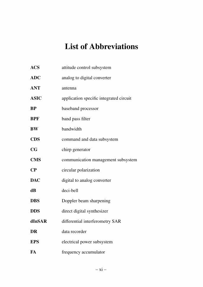
List of Abbreviations
ACS attitude control subsystem
ADC analog to digital converter
ANT antenna
ASIC application specific integrated circuit
BP baseband processor
BPF band pass filter
BW bandwidth
CDS command and data subsystem
CG chirp generator
CMS communication management subsystem
CP circular polarization
DAC digital to analog converter
dB deci-bell
DBS Doppler beam sharpening
DDS direct digital synthesizer
dInSAR differential interferometry SAR
DR data recorder
EPS electrical power subsystem
FA frequency accumulator
– xi –
FCW frequency control word
FFT fast Fourier transform
FM frequency modulation
FPGA field programmable gate array
GNSS Global Navigation Satellite System
GSE ground supporting equipment
HPA high power amplifier
IF intermediate frequency
IMU inertial momentum unit
InSAR interferometry SAR
IRF impulse response function
ISLR integrated side lobe ratio
ISP image signal processing
KOMPSAT-5 Korea multi purpose satellite-5
LEO low Earth orbit
LFM linear frequency modulation
LNA low noise amplifier
LO local oscillator
LP linear polarization
LPF low pass filter
LUT look up table
MTC mode and timing controller
– xii –
NESZ noise equivalent sigma zero
OBC on-board computer
PA phase accumulator
PDDS parallelized direct digital synthesizer
PDU power distribution unit
PLL phase locked loop
PRF pulse repetition frequency
PROM programmable read only memory
PSD power spectrum density
PSInSAR persistent scatterer interferometry SAR
PSLR peak to side lobe ratio
RAR real aperture radar
RF radio frequency
RMSE root mean square error
ROM read only memory
Rx reception
SAR synthetic aperture radar
SNR signal to noise ratio
SSD solid state drive
SSPA solid state power amplifier
TC timing controller
TM/TC telemetry and telecommand
– xiii –

Tx transmission
UAV unmanned aerial vehicle
VCO voltage controlled oscillator
– xiv –

Chapter 1. Introduction
1.1 Background and Motivation
Synthetic aperture radar (SAR) system is designed to generate the image of tar-
gets in remote area using microwave signal [1] and [2]. Because SAR supports the
high-resolution target images in all-weather condition, it is recognized as powerful
surveillance radar system. SAR uses the linearly frequency modulated (LFM) mi-
crowave signal called chirp so that it can penetrate the clouds over interested area.
Unlikely to optical sensors SAR transmits and receives its observation signal, there-
fore it can be operated regardless of day-night condition [3], [4]. Compared to optical
sensor, the pixel information from SAR has not only amplitude value but also phase
information. Generally, microwave signal consists of amplitude and phase. When
SAR generates target image, the output contains amplitude and phase information.
Among those two information, amplitude represents the intensity of SAR image. On
the other hand, the user can not recognize phase information by looking output im-
age. Phase information underlying each pixel can be utilized several fields such as
land deformation.
The microwave signal transmitted from antenna reflects on the target in remote
area. In this situation, according to the target characteristic the signal amplitude
and phase get change. Although SAR has only black and white colors on its image
as shown in Figure 1.1, SAR images are used in various applications by using am-
– 1 –

Figure 1.1. Example of SAR image of Pyeong-yang, North Korea.
plitude and phase information in each pixel [?]. Interferometry SAR (InSAR), the
persistent scatterer InSAR (PSInSAR), and differential InSAR (dInSAR) are repre-
sentative SAR applications. Those applications can be used to analyze land defor-
mation, environmental observation, resource exploration, disaster monitoring, and
etc.
L-(1-2 GHz), C-(4-8 GHz), and X-band (8-12 GHz) are commonly used mi-
crowave band for transmission signal of SAR. Each band has its own wavelength:
– 2 –
approximately 23 cm, 5.7 cm, and 3 cm, respectively. However, if platform posi-
tion changes from flight path more than their wavelength the phase information of
received signal would not be accurate [5].
One characteristic of SAR system is that it observes the target in perpendicular
to the its flight path. During the SAR on-board platform on-the-move, SAR system
transmits and receives it own signal. It has several operational modes such as strip-
map mode, spotlight mode, scan mode, and etc. The most general mode is strip-map
and it scans the area of interest without beam steering.
SAR supports high resolution images by using the antenna synthesis technique
in azimuth direction and linear frequency modulation (LFM) in range direction. Syn-
thetic antenna synthesis indicates a technique that is achieved during SAR operation.
Larger the antenna length better the resolution is commonly known radar principle.
Bus system which has SAR moves along its flight path above the target and transmits
microwave signal continuously. The antenna loaded on SAR has actual dimension,
however during SAR mission, the length of moving trajectory of bus system indi-
cated its synthesized antenna length. By doing so, SAR can achieve high resolution
in azimuth direction. The microwave signal that SAR adopts is called LFM signal or
chirp. For imaging radar, wide bandwidth is required to get higher resolution images
because the resolution of radar image is inverse proportional to bandwidth. The in-
stantaneous frequency of chirp increases linearly with time therefore SAR uses chirp
for its illumination signal.
Recently requirements over the resolution of SAR system is sub-meter class
(less than 1 m) and required bandwidth is increasing up to 300 MHz [6] and [7].
– 3 –
Therefore the wideband chirp signal generator with high-reliability is needed to sup-
port high-resolution SAR images. Generally speaking, wider the bandwidth of signal
worse the imbalance components which comes from RF units. Those imbalances de-
grades the quality of transmit signal and eventually the resolution of SAR image
suffers from noise. Therefore it is important to choose a stable system to improve the
quality of transmit signal [8].
1.2 Contributions
This dissertation aims to propose a design scheme for a SAR system and the
novel phase error compensation algorithm for direct digital synthesizer (DDS) chirp
generator by using polynomial modeling method. The proposed design scheme is
presented with a parameter calculation simulator which is able to reduce the itera-
tion procedure during SAR system parameter calculation by using minimum users’
requirements. Also the proposed simulator in this dissertation gives antenna size
minimization method to SAR system designer.
In addition, this dissertation analyze the phase shift error which occurs during
digital signal generation stage called truncation process. It shows that truncation gen-
erates spurious that should be eliminated. The proposed novel phase error compensa-
tion algorithm calculates the deterministic phase error by using polynomial modeling
and compensates the error with compensation coefficients. From simulation and ex-
periment, the proposed algorithm in this dissertation shows that it can eliminate the
spurious components ideally and enhance the impulse response function (IRF) char-
– 4 –

acteristics.
The followings are the principal contributions of this dissertation:
• Structures of satellite system and SAR system are presented.
• SAR system calculation simulator has been proposed.
• The design method which can minimize the antenna aperture is proposed.
• Relationship between truncation and spurious of chirp signal has been ana-
lyzed.
• DDS and parallel DDS (PDDS) type chirp generator is proposed.
• Novel phase error compensation algorithm which can eliminate the spurious
components has been proposed.
• DDS and PDDS chirp generator have been implemented using field programmable
gate array (FGPA).
• With the help of phase compensation algorithm, the proposed PDDS chirp
generator has shown better performance in both simulation and experiment in
the respect of phase shift, spurious, impulse response function (IRF), and point
target analysis.
1.3 Overview
The remainder of this thesis is organized as follows. In Chapter 2, an overview
of radar system, fundamentals of SAR sytem and characteristics of chirp signal gen-
– 5 –

erator are described. Also, previously proposed DDS chirp signal generators are
described. The Chapter 3 shows the SAR system design procedure and presents
important system design parameters. The structure of the proposed chirp signal gen-
erator, the phase error of conventional DDS chirp generator, the proposed phase error
compensation algorithm are folled in Chapter 4. The performance analysis between
conventional DDS chirp signal generator and the proposed chirp signal generator
in simulation experiment will be presented either. This dissertation is concluded in
Chapter 5.
– 6 –
Chapter 2. Related Works
In this chapter, a brief overview on SAR system and the characteristics of chirp
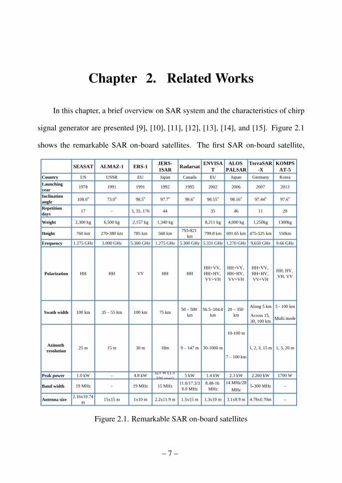
signal generator are presented [9], [10], [11], [12], [13], [14], and [15]. Figure 2.1
shows the remarkable SAR on-board satellites. The first SAR on-board satellite,
SEASAT ALMAZ-1 ERS-1JERS-1SAR
RadarsatENVISA
TALOS
PALSARTerraSAR
-XKOMPS
AT-5
Country US USSR EU Japan Canada EU Japan Germany Korea
Launchingyear
1978 1991 1991 1992 1995 2002 2006 2007 2013
Inclinationangle
108.0o 73.0o 98.5o 97.7o 98.6o 98.55o 98.16o 97.44o 97.6o
Repetitiondays
17 - 3, 35, 176 44 35 46 11 28
Weight 2,300 kg 6,500 kg 2,157 kg 1,340 kg 8,211 kg 4,000 kg 1,250kg 1300kg
Height 760 km 270-380 km 785 km 568 km793-821
km799.8 km 691.65 km 475-525 km 550km
Frequency 1.275 GHz 3.000 GHz 5.300 GHz 1.275 GHz 5.300 GHz 5.331 GHz 1.270 GHz 9,650 GHz 9.66 GHz
Along 5 km 5 - 100 km
Across 15, 30, 100 km
Multi mode
10-100 m
7 – 100 km
Peak power 1.0 kW - 4.8 kW325 W (1.3
kW spec)5 kW 1.4 kW 2.3 kW 2.260 kW 1700 W
14 MHz/28
MHz
Antenna size2.16x10.74
m15x15 m 1x10 m 2.2x11.9 m 1.5x15 m 1.3x10 m 3.1x8.9 m 4.78x0.70m -
20 – 350 km
Azimuth resolution
25 m 15 m 30 m 18m 9 – 147 m 30-1000 m
HHHH+VV, HH+HV, VV+VH
HH+VV, HH+HV, VV+VH
Swath width 100 km 35 – 55 km 100 km 75 km50 – 500
km56.5–104.8
km
Polarization HH HH VV HHHH+VV, HH+HV, VV+VH
HH, HV, VH, VV
Band width 19 MHz - 19 MHz 15 MHz11.6/17.3/3
0.0 MHz8.48-16
MHz5-300 MHz -
1, 2, 3, 15 m 1, 3, 20 m
Figure 2.1. Remarkable SAR on-board satellites
– 7 –
SEASAT from US, had been launched on 1978. In that time, the operational center
frequency of observation signal was located in L-band (1.275 GHz). Also, the signal
bandwidth was only 19 MHz wide therefore the spatial resolution was around 10
m by rough calculation. Less than two decades later, Japan had launched their first
JERS-1 on 1992. It is also operated on the same center frequency as SEASAT. Due to
the lager antenna size, JERS-1 supports better azimuth resolution than SEASAT. We
can notice that the operational center frequency goes up according to launching year.
Recently, X-band (8-12GHz) is commonly used for center frequency to observe the
target in interest more precisely. TerraSAR-X and KOMPSAT-5 are the remarkable
examples of X-band SAR. They are equipped with the phased array antenna with
beam steering capability. The bandwidth has been expanded up to 300 MHz therefore
those SAR satellites can offer fine resolution target images to users. Also, we can take
a look on the trends over polarization. At the beginning of SAR system development
stage, usual SAR systems adopted single polarization such as HH or VV (where
the first and second capital letters indicate the polarization plane of received and
transmitted signal respectively) [16]. However, from around 2000, ENVISAT from
EU has shown dual and full polarization modes. The impact of multi-polarization is
that SAR system can acquire much information from complex scatterers in remote
area. Therefore the users can utilize huge amount of information from several targets.
The trend on SAR payload development is able to summarized as high-resolution,
multi-polarization, higher bandwidth, and etc.
– 8 –

Power
Amplifier
Waveform
Generator
T/R Switch
ReceiverA/D
Converter
Pulse
Compression
Clutter Rejection
(Doppler Filtering)
DetectionThresholdingParameter
EstimationTracking
Data
Recording
Antenna
Transmitter
Signal Processor Computer
General Purpose Computer
Figure 2.2. Basic structure of radar system
2.1 Structure of common radar system
General radar system structure is shown in 2.2. Radar system consists of trans-
mitter, T/R switch, antenna, receiver, A/D converter, signal processor computer, gen-
eral purpose computer, and data recorder. Transmitter generates transmission signal
by using waveform generator and power amplifier. In the case of single antenna radar
system as shown in figure 2.2, T/R switch controls transmit and reception window.
Antenna transmits the generated signal to target and receives back-scattered signal.
Back-scattered signal in receiver stage is processed into digital data by A/D converter.
Signal processor compresses received signal using transmitted signal. Basically radar
– 9 –

system requires to detect target in far distance with high resolution. First, radar sys-
tem requires high-powered transmission signal to achieve long distance detection so
that the transmitted pulse can travel further. Second, radar system should generate
narrow pulse to support high-resolution detection. However, both requirements are
physically hard to implement in hardware because of cost, system complexity, and
etc. Therefore radar system conducts post processing to compress the received pulse
in reception stage. SAR system is similar to the structure of general radar systems.
2.2 SAR System Design
2.2.1 Geometry Model of SAR System on Mission
In this dissertation, we will consider both space-borne and airborne SAR sys-
tems. As discussed before, SAR system transmits and receives chirp signal during
operation as depicted in figure 2.3. The path which SAR system moves along is
called as platform direction or commonly azimuth direction. In addition, the axis
which is perpendicular to azimuth direction is called range direction [17, 18, 19, 1].
When SAR system transmits its signal, the transmitted signal is overlaid on target
area as shown in figure 2.3. The usable nearest and most far beam footprint over
ground are called near range and far range respectively.
The observation modes of SAR are determined by the beam steering methods.
Representatively, there are three modes; the strip-map mode, scan mode, and spot-
light mode. The strip-map mode which is the most common observation mode is
considered in this thesis. Also, when designing SAR system, the polarization which
– 10 –
SAR sensor
Near range
Far range
Figure 2.3. Side looking of SAR system on the move.
means the difference between electric and magnetic wave should be considered.
2.2.2 Basic Structure of SAR Payload System
This section describes a general satellite system which can be divided as bus
system and payload. The satellite system consists of the payload, attitude control
subsystem (ACS), electrical power subsystem (EPS), command and data subsystem
(CDS), and communication management subsystem (CMS). The bus system indi-
cates the integration of ACS, EPS, CDS, and CMS. SAR system is installed in pay-
load as a subsystem of satellite system. ACS controls the attitude of satellite by
using the reaction wheels and momentum gyro. EPS distributes charged power to
other subsystems. CDS controls the telemetry and tele command between satellite
subsystems. Finally, CMS communicates with ground stations using S and X-bands.
– 11 –
SA
R
LV
PS
Pro
cess
or
Mod
ule
IO
Mod
ule
LV
PS
Mem
ory
IO
Mod
ule
Mem
ory
Mod
ule
#1
ST
X
LV
PS
XT
X
SR
X
LV
PS
So
lar
Pa
nel
PD
U
CS
ST
AM
CS
ST
AM
Gy
ro
ST
RU
XT
U
Ba
tter
y
Po
wer C
on
trol
Un
itP
ow
er D
istr
ibu
tio
n U
nit
EP
SC
DS
CM
S
AC
SP
aylo
ad
Actu
ato
rs
Rea
ctio
n
Wh
eel
Torq
ue
Bar
EM
TD
Sen
sors
Sola
r p
ow
er
reg
ula
tor
Batt
ery
mon
itorin
g
+28
V B
US
RE
TU
RN
Mem
ory
Mod
ule
#2
S-A
NT
X-A
NT
+5V
/+15
V/+
28
V
Figure 2.4. Block diagram of satellite system.
– 12 –
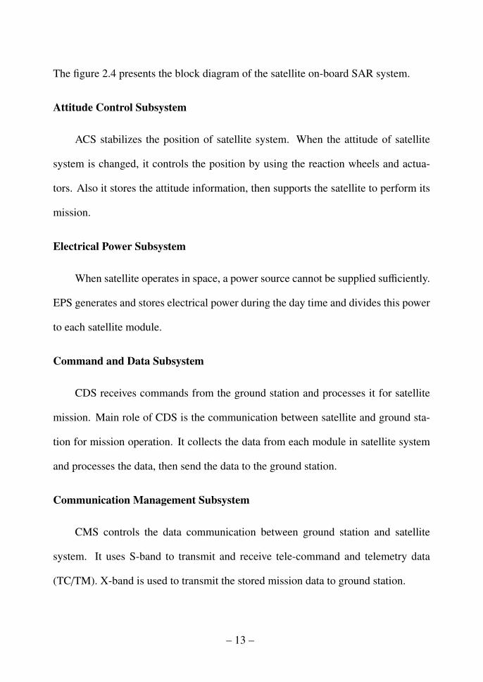
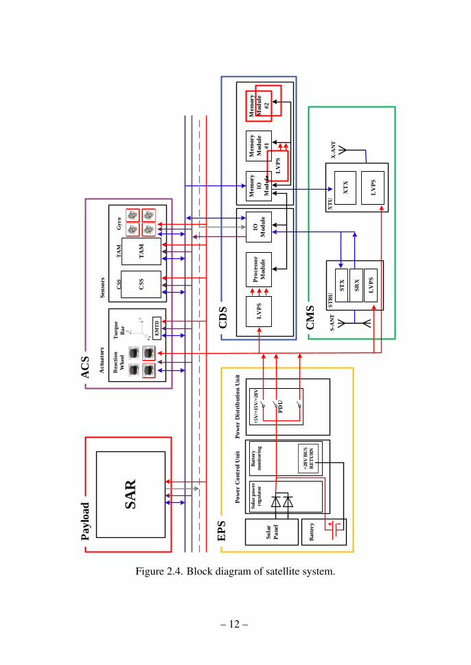
The figure 2.4 presents the block diagram of the satellite on-board SAR system.
Attitude Control Subsystem
ACS stabilizes the position of satellite system. When the attitude of satellite
system is changed, it controls the position by using the reaction wheels and actua-
tors. Also it stores the attitude information, then supports the satellite to perform its
mission.
Electrical Power Subsystem
When satellite operates in space, a power source cannot be supplied sufficiently.
EPS generates and stores electrical power during the day time and divides this power
to each satellite module.
Command and Data Subsystem
CDS receives commands from the ground station and processes it for satellite
mission. Main role of CDS is the communication between satellite and ground sta-
tion for mission operation. It collects the data from each module in satellite system
and processes the data, then send the data to the ground station.
Communication Management Subsystem
CMS controls the data communication between ground station and satellite
system. It uses S-band to transmit and receive tele-command and telemetry data
(TC/TM). X-band is used to transmit the stored mission data to ground station.
– 13 –
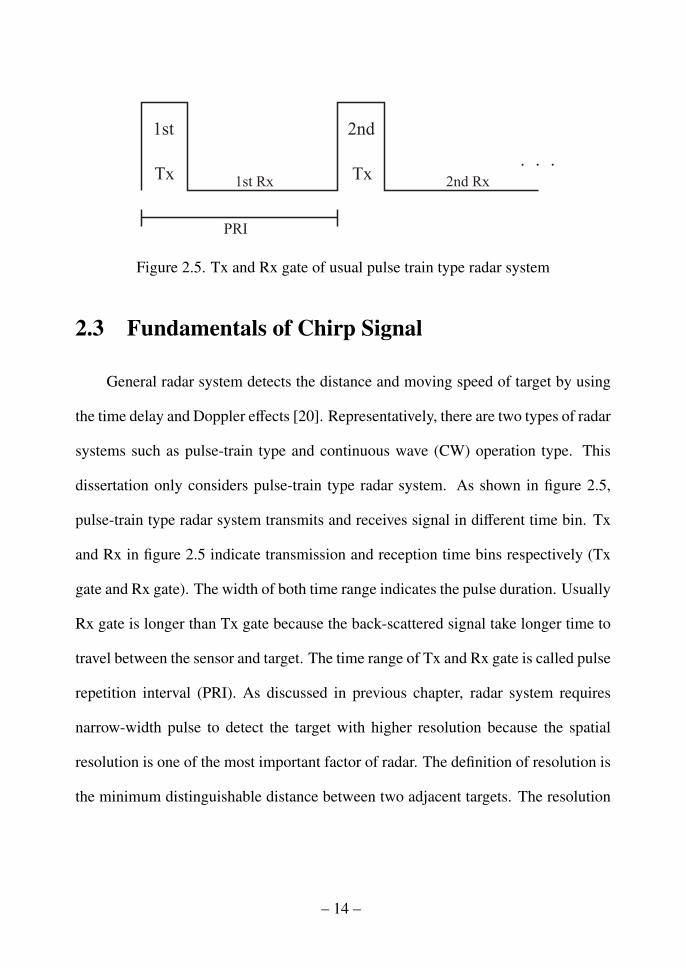
1st
1st Rx 2nd Rx
2nd
Tx
PRI
Tx
Figure 2.5. Tx and Rx gate of usual pulse train type radar system
2.3 Fundamentals of Chirp Signal
General radar system detects the distance and moving speed of target by using
the time delay and Doppler effects [20]. Representatively, there are two types of radar
systems such as pulse-train type and continuous wave (CW) operation type. This
dissertation only considers pulse-train type radar system. As shown in figure 2.5,
pulse-train type radar system transmits and receives signal in different time bin. Tx
and Rx in figure 2.5 indicate transmission and reception time bins respectively (Tx
gate and Rx gate). The width of both time range indicates the pulse duration. Usually
Rx gate is longer than Tx gate because the back-scattered signal take longer time to
travel between the sensor and target. The time range of Tx and Rx gate is called pulse
repetition interval (PRI). As discussed in previous chapter, radar system requires
narrow-width pulse to detect the target with higher resolution because the spatial
resolution is one of the most important factor of radar. The definition of resolution is
the minimum distinguishable distance between two adjacent targets. The resolution
– 14 –
of radar in range direction can be defined as,
r =cT2, (2.1)
where r, c, and T are range resolution, the speed of light, and pulse width, respec-
tively. (2.1) indicates that resolution factor gets better when pulse width gets nar-
rower. Therefore radar system should have small T value to achieve better resolution
(r). Implementing the radar system with narrow pulse width is physically hard when
considering switching time and etc. Therefore, radar system adopts pulse compres-
sion technique on signal processing stage in receiver. Back-scattered signal from
target passes through matched filter, then the effective pulse width gets narrower by
post processing. Assuming the transmitted chirp signal s(t) is given by (2.2), the
back-scattered signal with a time t0 later sr(t) can be expressed as (2.3)
s (t) = rect( tT
)exp
{jπKt2
}(2.2)
sr (t) = rect( t − t0
T
)exp
{jπK(t − t0)2
}, (2.3)
where t, T, and K are time, pulse width, and signal sweep rate, respectively. When
expressing the impulse function of matched filter (h(t)) as
h (t) = rect( tT
)exp
{−jπKt2
}, (2.4)
then matched filter output sout(t) can be expressed as (2.5) and it indicates rectangular
signal has been transformed to sinc function
sout (t) ≈ T sinc (KT (t − t0)) . (2.5)
– 15 –

Figure 2.6. Sinusoid and chirp signals.
Finally, if we assume the 3-dB beam width of sinc signal as τcomp, the range resolution
after pulse compression will be as
r =cτcomp
2≈
1|K|T
. (2.6)
Because |K|T is the signal bandwidth, (2.6) indicates that resolution of radar can be
enhanced when the signal has wide-bandwidth [21].
Figure 2.6 shows the comparison between the single-tone sinusoid and chirp
signal. Each signal in figure 2.6 has the pulse width of T. Because sinusoid has
single-tone frequency, we can define the bandwidth of sinusoid as 1/T . On the other
hand, instantaneous frequency of chirp increases linearly within time T. Assuming
that the value of starting and end frequency of chirp are F1 and F2 respectively, the
bandwidth would be expressed as F2 − F1. Expanding the equation with Euler’s
formula, (2.2) can be expressed as
s (t) = rect( tT
) {cos
(πKt2
)+ j sin
(πKt2
)}, (2.7)
– 16 –

where πKt2 is the phase component of chirp signal. The cosine term is called real or
in-phase signal and we denote this term as I data. Also, the sine term is an imaginary
part of signal and called Q data. For the simplicity, we only consider the real term (I
data) in -1 to 1 range. The I data of chirp signal is defined as
sreal (t) = |s (t)|−1≤t≤1 = cos(πKt2
)= cos (φ (t)) . (2.8)
The derivative of phase term φ (t) indicates the instantaneous frequency of chirp sig-
nal and it is shown in (2.9).
f (t) =1
2πdφ (t)
dt=
12π
d(πKt2
)dt
= Kt (2.9)
Mathematical results above indicate that the instantaneous frequency of chirp
signal increases linearly to the time t. Therefore, by setting the chirp rate (or sweep
rate) K, a user can modify the bandwidth of chirp signal easily. As shown in (2.6),
if a chirp signal occupies the wide band width, the resolution of SAR system can be
enhanced. Thus recent SAR system requires to generate the wide-bandwidth chirp
signal to support high-resolution image [22].
2.4 Chirp Signal Generator
As a kind of arbitrary waveform generator (AWG), the chirp signal generator re-
quires high stability, frequency linearity, fast frequency response, low FM noise, and
etc [20, 23]. The procedure of SAR image processing consists of FFT and matched
filtering between transmission chirp and back-scattered signal [24]. There are largely
two requirements for SAR system when generating chirp. First, SAR system requires
– 17 –
to generate ideal-like chirp as possible so that the matched filter output would main-
tain sufficient SNR. Second, chirp output should have sufficiently wide bandwidth
within Shannon’s capacity (sampling theorem) to have high resolution [25]. There
exist several types of chirp generator to support stable and wide-bandwidth signal.
In this section, representative chirp generators and the characteristics of direct digital
synthesizer (DDS) chirp generator will be discussed.
2.4.1 Memory-map Based Chirp Signal Generator
A designer should consider several constraints when designing signal generator
for satellite or aircraft payload such as size (volume), weight, power consumption,
and etc. Those constraints are always required to be small as possible. Signal gen-
erator using voltage controlled oscillator (VCO) had been used before, however it is
no more used as payload because of its large size and heavy weight. To minimize
the size and weight of chirp generator, various types of signal generators have been
introduced. Compare to the analog VCO type generator, digital signals generator
such as application specified integrated circuit (ASIC) or field programmable gate
array (FPGA) less occupy the space for payload. Among several digital signal gener-
ators, there exists the memory-map based signal generator. The conventional satellite
on-board SAR system has used the memory-map based chirp signal generator [26].
The memory-map based signal generator stores predefined waveform in its storage
then reconstructs output signal. Because memory-map signal generator consists of
memory unit and digital-to-analog converter (DAC), the signal generation process
becomes simple and the accuracy of signal show ideal-like characteristic.
– 18 –
Memory
ROM (I)
Clock
source
Counter
PLL
PRFMemory
ROM (Q)
DAC
DAC
Recon
stru
ctio
n
filter
I data
Q data
Figure 2.7. Structure of memory-map based chirp signal generator.
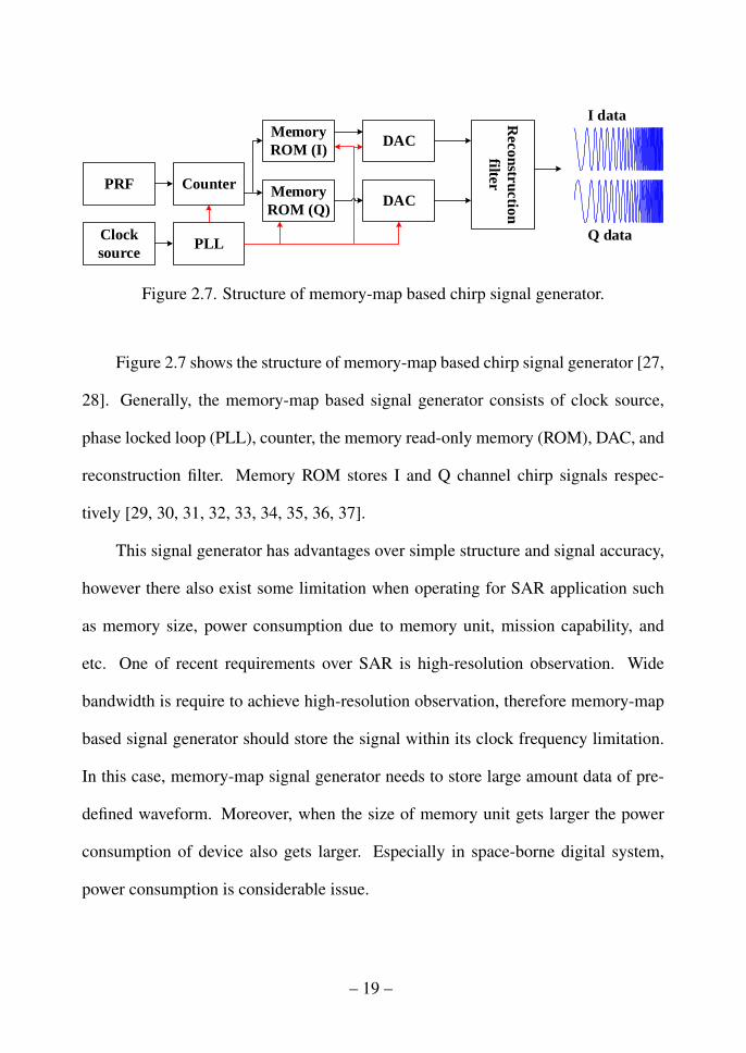
Figure 2.7 shows the structure of memory-map based chirp signal generator [27,
28]. Generally, the memory-map based signal generator consists of clock source,
phase locked loop (PLL), counter, the memory read-only memory (ROM), DAC, and
reconstruction filter. Memory ROM stores I and Q channel chirp signals respec-
tively [29, 30, 31, 32, 33, 34, 35, 36, 37].
This signal generator has advantages over simple structure and signal accuracy,
however there also exist some limitation when operating for SAR application such
as memory size, power consumption due to memory unit, mission capability, and
etc. One of recent requirements over SAR is high-resolution observation. Wide
bandwidth is require to achieve high-resolution observation, therefore memory-map
based signal generator should store the signal within its clock frequency limitation.
In this case, memory-map signal generator needs to store large amount data of pre-
defined waveform. Moreover, when the size of memory unit gets larger the power
consumption of device also gets larger. Especially in space-borne digital system,
power consumption is considerable issue.
– 19 –

Tuning
word
System
clock
Phase
register
Cosine
LUT
Sine
LUT
DAC
DAC
Phase accumulator Output
(I)
Output
(Q)
Figure 2.8. Structure of DDS signal generator.
2.4.2 DDS Chirp Signal Generator
DDS type signal generator is introduced to overcome the disadvantages of memory-
map signal generator and to be used as arbitrary waveform generator (AWG). The
structure of DDS signal generator is presented in figure 2.8 [27, 38, 21]. It consists
of clock source, register, look-up table (LUT), and DAC. The input signal is called
tuning word or frequency tuning word (FCW). FCW in DDS signal generator is con-
stant input in binary data form. FCW is accumulated in phase register continuously
according to system clock. Therefore phase register works similar to mathematical
integrator and is called phase accumulator. In case of basic DDS sinusoid signal
generator as depicted in figure 2.8, phase accumulator generates ramp signal output
because FCW is accumulated continuously along each clock. Then cosine and sine
LUTs which are a kind of PROM converts phase signal into sinusoid using the stored
phase to amplitude information. DAC at the end point reconstructs digital signal
into analog signal. Further information regarding to conventional DDS chirp signal
– 20 –
generator will be discussed in Chapter 4.
2.5 Summary
In this chapter, a brief overview of radar systems is presented. From the intro-
duction to the structure of common radar system, this chapter introduced the general
radar systems including SAR. Also the design procedure of SAR system has been
presented in section 2.2. Fundamental of chirp signal and digital signal generators
including the memory-map based signal generator and DDS signal generators are
presented.
– 21 –
Chapter 3. Design of SAR system
Synthetic aperture radar (SAR) has been used widely in the field of remote sens-
ing such as surveillance, land deformation research, urban managing, disaster mon-
itoring, and etc [39]. It supports high-resolution images of target regardless of light
and the weather condition. Usually, the SAR payload operates its mission on moving
platforms such as satellite, unmanned aerial vehicle (UAV), airplane, car and etc. It
transmits and receives microwave signal called chirp. The chirp signal is a kind of
linear frequency modulated (LFM) signal and its instantaneous frequency increases
or decreases linearly with time. The resolution of general radar systems is inverse
proportional to the signal bandwidth. It indicates that the radar system with wider
bandwidth can offer the higher resolution. The SAR can support the high resolution
images by adopting the chirp signal.
There are several satellite or UAV on-board SARs in mission. Because the SAR
acquires the images on the move, the satellite on-board SARs usually operate its
mission on the low-Earth orbit (LEO: 500 – 800 km). The satellite on-board SAR
has several advantages on the stable operation, wide-area monitoring, and etc. How-
ever, the disadvantages also exist when the SAR is implemented on satellite platform.
First, the performance of the space environment validated components is lower than
commercial components. Second, tremendous time and budget cost are needed on
system development. In general case, it takes approximately 5-year to develop and
– 22 –
launch the satellite system. During the satellite system development phase, the ver-
ification on the qualification model (QM) and flight model (FM) is required and
consequently it leads to the high budget and time cost.
To conduct the continuous and intensive monitoring on specific areas, the UAV
on-board SAR is preferred for the high resolution imaging. Various UAV on-board
SAR already exist in research fields and some of them are on practical mission. Com-
pare to the satellite platform, UAV on-board SAR perform its mission on 1 - 10 km
above the ground and the stratosphere mission (>10 km) is being considered recently.
The types of SAR systems can also be classified into microwave bands. Among the
wide range of microwave from L-band (1-2 GHz) to Ku-band (24-40 GHz), each
band has specific usage and characteristic. L-band has relatively longer wavelength
than other bands; approximately 23 cm. Due to its wavelength characteristic, L-band
SAR is suitable to land deformation research, interferometry application, resource
exploration, and etc. However, the frequency allocation of L-band is quite narrow
(bandwidth = 40-85 MHz), so that L-band SAR cannot offer the high resolution im-
age. In addition, when designing the antennas, it requires relatively larger size than
other bands. Because the usual UAV has rigid constraint on its payload size, the
higher frequency bands are preferred for UAV on-board SAR. Hence, X-band (8-10
GHz) SAR has been designed in this paper. The frequency allocation for remote
sensing on X-band has the range upto 800 MHz.
The demands on UAV or plane on-board SAR are increasing because of its ver-
satility to missions [40]. In the meantime, the high performance and stability of SAR
are also required. Therefore, the system optimization as well as SAR system design
– 23 –
technique are important issues. When designing the UAV on-board SAR systems,
there are several types of constraints to be considered such as the mountable pay-
load size, the flight scenario of UAV, geometry between platform and target, power
consumption, SAR system parameters, and etc.
SAR is complicated system which consists of digital circuits, RF subsystems,
antennas, and etc. When designing SAR system, the designer should consider its
operational concept, design budget, specification, interface, and etc. Therefore it
requires several iterations on operational concept design and parameter calculation.
This chapter presents the analysis on SAR system design requirements, the design
procedure of SAR system, comparison between existing SAR systems, and etc.
The flow chart of SAR system design parameter is presented in figure 3.1 [40]
– 24 –

Figure 3.1. Flow chart of SAR system design parameters– 25 –
SAR system design starts from requirements analysis. A designer should con-
sider the top-level requirement such as platform specification and performance. There
are several kinds of platforms therefore weight, mission altitude, platform velocity,
the maximum mountable antenna size, and other parameters should be considered
precisely. Because signal bandwidth is the most significant factor of resolution, sig-
nal properties such as pulse width and bandwidth are decided on this stage.
After the maximum mountable antenna size is confirmed, a designer considers
antenna constraints. This stage includes the length and size of antenna, antenna gain,
azimuth and range beam width, antenna efficiency, and etc.
Geometry parameter calculation follow next. In this stage the geometry be-
tween SAR platform and target on ground (Earth) is considered. Considerable items
are incidence angle, ground swath according to antenna specification, slant range
according to altitude and target distance, and etc.
Using the parameters from previous design stage, SAR system designer decides
pulse repetition frequency (PRF) next. To avoid from the collision of microwave
signals, PRF is considered. PRF parameter is used in RF subsystem design.
Image resolution in range and azimuth direction is considered next. Range res-
olution is closely related to signal bandwidth and geometry parameters. On the other
hand, azimuth resolution is related to antenna constraint and platform specification.
To transmit and receive the specified microwave signals, SAR system requires
RF subsystem which generates proper signal. Considering the slant range and pay-
load weight, peak power is considered. Also using the azimuth beam width and plat-
form velocity, designer can decide azimuth pulse width. Generally maximum duty
– 26 –
cycle is limited to 10 %. System losses contains both hardware (H/W) and software
(S/W) loss.
After the conceptual system design is finished, performance evaluation process
remains. To assure the required specification the performance evaluation parame-
ters should be investigated such as noise equivalent sigma zero (NESZ), range and
azimuth ambiguity, resolution, signal noise ratio (SNR), and etc.
If the performance evaluation parameters satisfy the requirement, the conceptual
SAR system design finishes. In other case, however, several times of iteration are
required. Usually, by setting the PRF with proper value a designer can reduce the
time consumed on iteration process.
This chapter presents SAR system design parameters. SAR system design pro-
cedure for UAV and satellite shares same design process. In case of satellite on-
board system design, a designer usually verify the flight model by using aircraft first.
Therefore, this chapter handles both UAV and satellite on-board SAR system design.
3.1 Design Requirements
There are several requirements on SAR system design such as size, weight,
operational concept, and etc. This chapter discusses regarding to the requirements
and specification of SAR system design.
3.1.1 Operational Concept Overview and Requirement Analysis
When designing SAR system, a designer defines operational concept and mis-
sion requirements first. In this step, mission concept and scenario and requirements
– 27 –
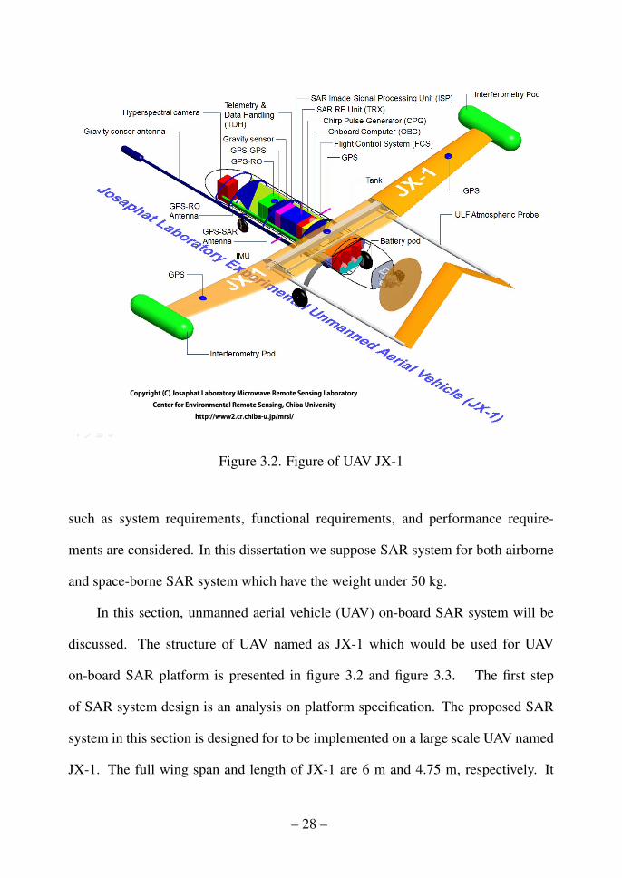
Figure 3.2. Figure of UAV JX-1
such as system requirements, functional requirements, and performance require-
ments are considered. In this dissertation we suppose SAR system for both airborne
and space-borne SAR system which have the weight under 50 kg.
In this section, unmanned aerial vehicle (UAV) on-board SAR system will be
discussed. The structure of UAV named as JX-1 which would be used for UAV
on-board SAR platform is presented in figure 3.2 and figure 3.3. The first step
of SAR system design is an analysis on platform specification. The proposed SAR
system in this section is designed for to be implemented on a large scale UAV named
JX-1. The full wing span and length of JX-1 are 6 m and 4.75 m, respectively. It
– 28 –
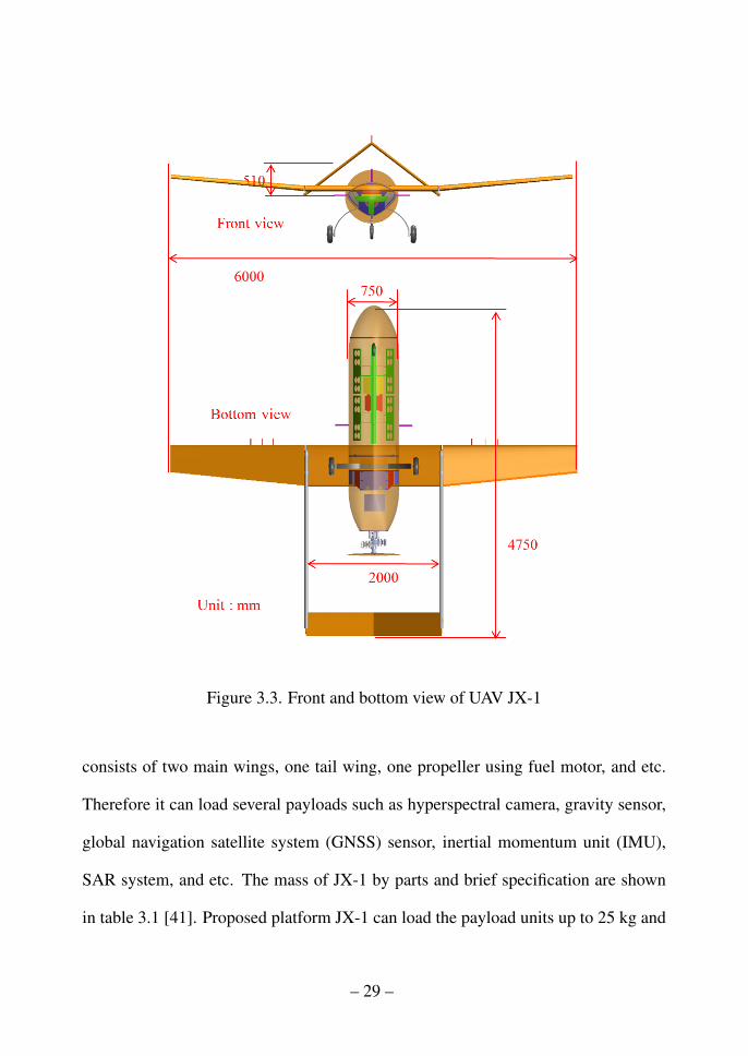
Figure 3.3. Front and bottom view of UAV JX-1
consists of two main wings, one tail wing, one propeller using fuel motor, and etc.
Therefore it can load several payloads such as hyperspectral camera, gravity sensor,
global navigation satellite system (GNSS) sensor, inertial momentum unit (IMU),
SAR system, and etc. The mass of JX-1 by parts and brief specification are shown
in table 3.1 [41]. Proposed platform JX-1 can load the payload units up to 25 kg and
– 29 –
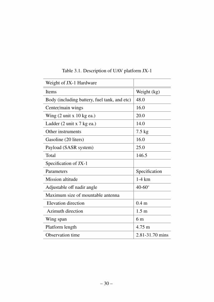
Table 3.1. Description of UAV platform JX-1
Weight of JX-1 Hardware
Items Weight (kg)
Body (including battery, fuel tank, and etc) 48.0
Center/main wings 16.0
Wing (2 unit x 10 kg ea.) 20.0
Ladder (2 unit x 7 kg ea.) 14.0
Other instruments 7.5 kg
Gasoline (20 liters) 16.0
Payload (SASR system) 25.0
Total 146.5
Specification of JX-1
Parameters Specification
Mission altitude 1-4 km
Adjustable off nadir angle 40-60◦
Maximum size of mountable antenna
Elevation direction 0.4 m
Azimuth direction 1.5 m
Wing span 6 m
Platform length 4.75 m
Observation time 2.81-31.70 mins
– 30 –
store 20 liters of gasoline. Nominal mission altitude is 1 - 4 km above the ground
and mission velocity (cruising speed) is 23 m/s.
As shown in figure 3.1, a designer compromises the requirements between plat-
form specification and signal properties. Once the platform is specified for mission,
signal properties such as pulse width, signal bandwidth, resolution bit, and center
frequency are considered. For more information, compare to the airborne platform
which has its own cruising speed, satellite on-board payload should calculate its ve-
locity (vst) as follow.
vst =
√G · Mt
Rt + h, (3.1)
where G, Mt, Rt, and h are gravitational constant, the mass of Earth, the Earth radius,
and altitude respectively. Generally, SAR payload is loaded on LEO satellite where
the altitude is 600 km high above from Earth ground. In this case, satellite platform
moves along its flight path with the velocity of 7 km/s.
After the analysis on platform specification is confirmed, the consideration over
signal properties follows next. In signal concept design, designer would consider
four items: center frequency ( fc), bandwidth, uncompressed pulse width, and time
margin. For example, 1.27 GHz, 5.4 GHz, and 9.4 GHz are preferred center fre-
quency in case of L-band, C-band, and X-band, respectively. Bandwidth is limited to
each band and hardware complexity. In general, 15 MHz, 40 MHz are preferred in
L-band while 150 MHz and 300 MHz are preferred in C and X-band. Uncompressed
pulse width (τp) should consider the minimum detectable distance. Time margin
(τmargin) indicates the sum of guard time during the rising and falling edge of signal.
– 31 –

Figure 3.4. Specification of existing UAV SAR
The slant range resolution of radar system (δel) is defined as,
δel =cτ2,=
c2B
(3.2)
where c, τ, and B are the speed of light, pulse width, and bandwidth, respectively. In
this dissertation, the center frequency and the signal bandwidth are set to 9.4 GHz and
800 MHz in UAV SAR case respectively. In this case, the ideal slant range resolution
will be 0.189 m. Compare to the existing UAV on-board SAR systems in figure 3.4,
the proposed SAR system has significantly higher resolution performance.
3.1.2 Analysis on Antenna Constraints
General radar systems prefer to use large aperture antenna because the larger the
antenna narrower the antenna beam width. To achieve better resolution antenna beam
width should be designed as narrow as possible. Figure 3.5 shows the comparison
of beam width and resolution between real aperture radar (RAR) and SAR. Because
the antenna beam width and antenna length are in inverse proportional, antenna with
large aperture has better resolution. However practical platform has the limitation
– 32 –

Figure 3.5. Comparison of beam width and resolution between real aperture radar
(RAR) and SAR
of antenna length. Therefore SAR synthesizes the back-scattered microwave in post
processing stage during operation.
The transmission (Tx) and reception (Rx) antennas transmit and receive the mi-
crowave signal. In general, when assuming the planar antenna shape, the beam width
of antenna has relationship between wavelength and the length and width of antenna
as
θaz = 0.88λ
L, θel = 0.88
λ
W, (3.3)
where θaz, θel, λ, L, and W are the 3-dB azimuth direction beam width, the 3-dB range
direction beam width, wavelength, the length and width of antenna, respectively.
Antenna gain (G) should be considered as
G = 4π ·ηAλ2 , (3.4)
– 33 –
where η, A, and λ are antenna efficiency (or radiation efficiency), antenna aperture,
and wavelength, respectively. When designing space-borne SAR, aperture efficiency
should be larger than 30 dB. In general, antenna efficiency (η) is 0.7 when considering
the worse case. A designer set the L and W within the limit of platform and iterate
the calculation result recursively till the result satisfies minimum antenna aperture.
The maximum mountable antenna size on JX-1 is 0.4 m x 1.5 m in elevation
and azimuth directions, respectively. The proposed SAR system considers the full
polarimetric antennas with two Tx antennas and two Rx antennas. The dimension
of one unit of antenna is 150 mm by 400 mm in elevation and azimuth directions,
respectively. According to the antenna size, the azimuth and range beam width can
be calculated using (3.3). Several types of antenna exist for SAR system, however,
the patched array antenna is considered in this dissertation. It has light weight and
easy to install and deploy.
3.1.3 Geometry Parameters
The SAR has significantly different geometry characteristics compare to other
radars or imaging sensors such as optical sensors, the visible near-infrared (VNIR)
sensors, and etc. It adopts side-looking method that the radar observes perpendicular
to the moving path but slightly tilted to the ground. Figure 2.3 shows the side-looking
method on the mission. The SAR on-board platform moves along the platform di-
rection. The line which is parallel to platform direction is called azimuth. Range
direction is perpendicular to the azimuth direction. SAR transmits a specific beam
to the ground. The area where transmitted beam is screened is shown in figure 2.3.
– 34 –
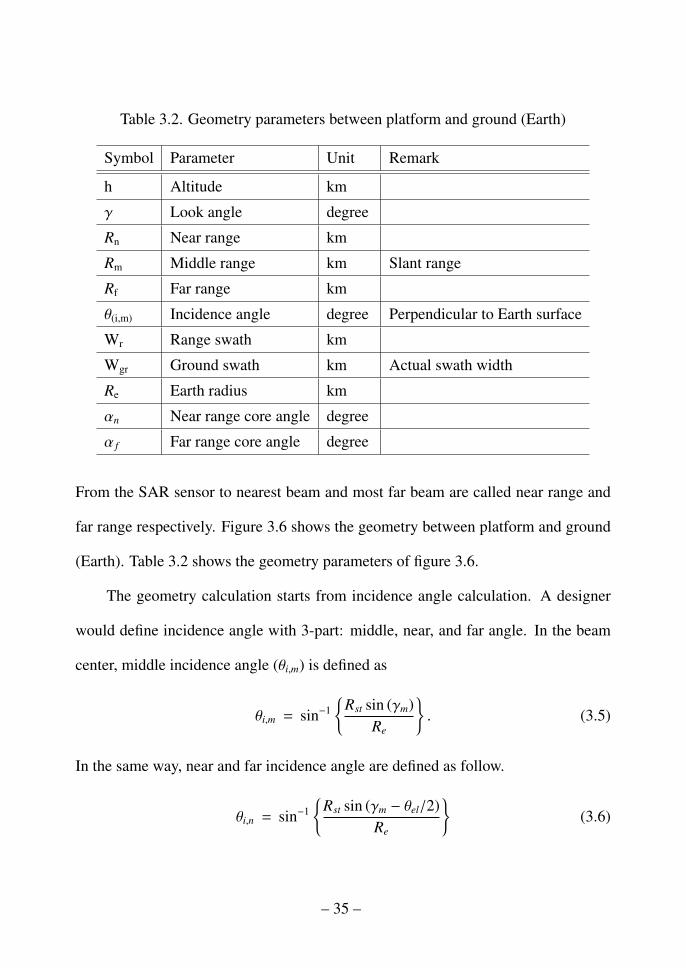
Table 3.2. Geometry parameters between platform and ground (Earth)
Symbol Parameter Unit Remark
h Altitude km
γ Look angle degree
Rn Near range km
Rm Middle range km Slant range
Rf Far range km
θ(i,m) Incidence angle degree Perpendicular to Earth surface
Wr Range swath km
Wgr Ground swath km Actual swath width
Re Earth radius km
αn Near range core angle degree
α f Far range core angle degree
From the SAR sensor to nearest beam and most far beam are called near range and
far range respectively. Figure 3.6 shows the geometry between platform and ground
(Earth). Table 3.2 shows the geometry parameters of figure 3.6.
The geometry calculation starts from incidence angle calculation. A designer
would define incidence angle with 3-part: middle, near, and far angle. In the beam
center, middle incidence angle (θi,m) is defined as
θi,m = sin−1{
Rst sin (γm)Re
}. (3.5)
In the same way, near and far incidence angle are defined as follow.
θi,n = sin−1{
Rst sin (γm − θel/2)Re
}(3.6)
– 35 –
Figure 3.6. Radar system geometry on orbit
– 36 –

and
θi, f = sin−1{
Rst sin (γm + θel/2)Re
}, (3.7)
where θel is elevation angle. Equations below present the calculation between geom-
etry parameters above.
Wr=Rf−Rn=Wgr sin(θi,m
), (3.8)
Rn =
√R2
e + R2s − 2ReRs cos (αn), (3.9)
R f =
√R2
e + R2s − 2ReRs cos
(α f
), (3.10)
γ = sin−1[Re sin
(θi,m
)Rs
], (3.11)
Rs = h + Re. (3.12)
Angle between the tilted antenna beam point and nadir point is called as off
nadir angle. This paper, the SAR system on JX-1 platform adopts the off nadir angle
of 45°. Considering the off nadir angle, the incidence angle to the ground (θi) can be
derived as
θi = sin−1{
h × sin (γm)Re
}, (3.13)
where h, γm and Re are the altitude of UAV, off nadir angle, and the Earth radius,
respectively [1]. The ground swath (Wgr) and the synthetic aperture length (Waz) can
be derived as
Wgr = Re × αs, (3.14)
– 37 –
Waz = 2 tan(θaz
2
), (3.15)
where Re and αs are Earth radius and the core angle of swath points, respectively.
3.1.4 Pulse Repetition Frequency and Resolution Parameters
Generally, the frequency modulated continuous wave (FMCW) SAR is fre-
quently used in UAV mission because of power consumption issues. However, the
proposed SAR system adopts pulsed Doppler radar. A pulsed Doppler radar divides
the Tx and Rx windows for signal acquisition. The collision between Tx and Rx sig-
nals during the mission distorts the received signal. To avoid from the problem, the
SAR system has the valid range of pulse repetition frequency (PRF). The minimum
and maximum PRFs are calculated as,
PRFmin =2vst sin (θaz)
cfc '
2vstθaz
λ'
2vst
L, (3.16)
PRFmax =1
[2τ + 2 (Rf − Rn) /c], (3.17)
where vst, fc, τ, Rf , and Rn are platform velocity, center frequency, pulse width, far
range time, and near range time, respectively [3]. Minimum PRF should be larger
than the Doppler bandwidth. Within the minimum and maximum range of PRF,
there are some other PRF area that radar system should avoid. In range direction,
SAR system should select the PRF to avoid the transmit and return collision. It can
– 38 –

be calculated as below,
N − 1
τn −(τmargin/2
)− τp
< PRF <N
τ f + τp + τmargin/2, (3.18)
where N indicates the number of transmit event. Also, in azimuth direction, some
sidelobe return components could collide in transmission. Therefore PRF also should
be ranged as below,
M − 1
τn −(τmargin/2
)− τp − τnadir
< PRF <M
τ f + τp +(τmargin/2
)− τnadir
, (3.19)
where M and τnadir indicate the number of transmit even in azimuth direction and the
return time from off-nadir angle. Generally designer choose the PRF value which
avoid those two return collision event time. The preferred PRF range is shown as,
1.25 × PRFmin <PRF< 0.75 × PRFmax. (3.20)
By using the PRF values above, one can derive the minimum acceptable antenna
aperture.PRFmin
PRFmax=
2vst
(2τp + 2
(R f − Rn
)/2
)L
(3.21)
We can derive ground swath in (3.14) as,
Wgr =(R f − Rn
)/ sin
(θi,m
). (3.22)
The radar beam width in the elevation angle can be expressed as,
λ/W =(Wg cos
(θi,m
))Rm. (3.23)
Using equations above the minimum antenna size is presented as
Amin =PRFmax
PRFmin
4λvstRm
ctan
(θi,m
). (3.24)
– 39 –

3.1.5 RF System Properties and Performance Evaluation
RF system modulates the Tx chirp signal using mixer unit and up-converts Tx
signal from base band to RF stage using high power amplifier (HPA). The RF system
properties effect the performance of radar system, therefore, the system constraints
such as peak power, maximum duty cycle, and system loss should be considered pre-
cisely. The system performance can be evaluated using signal-to-noise ratio (SNR)
and the noise-equivalent sigma zero (NESZ). The SNR can be expressed as,
SNR =PtGtArησ
(4π)2R4kTrNFBnLs
, (3.25)
where Pt, Gt, Ar, η, and σ indicate the peak transmission power, Tx gain, Rx gain,
antenna efficiency, and reflectance, respectively. Also R, k Tr, NF, Bn, λ, and Ls are
altitude, Boltzman constant, receiver temperature, noise figure, noise bandwidth, and
system loss, respectively. In the upper term of (3.25), Pt and σ are the variables.
SNR equation can be converted into other term such as,
SNR=PtτpPRFTDGtArησ
(4π)2R4kTrNFBnτcLs
, (3.26)
where τpPRF and TD are duty cycle and the synthetic aperture time. The constant TD
also can be expressed as,
TD =Rmθaz
vst. (3.27)
In usual case, SAR system designer tries to the value of Bnτc to be 1. Equation (3.26)
can be converted to
SNR =PavgA2
rxη2δelσ
0
8πR3kTrNFvstλLs
(3.28)
– 40 –

1. System requirements Value Unit Optional 4. Antenna constraints #1 Value Unit Optional 5. Geometry parameters Value Unit Optional 6. Swath Value Unit OptionalResolution Antenna design requirements Off nadir angle (g) g = 25° g = 35° g = 45° Theoritical slant range (km) g = 25° g = 35° g = 45°
Range resolution (dr) 10 m Required S11 (S11) Under -10 dB 25 35 45 Near range (Rn,thm) 10.9192747 12.0183516 13.8323389Azimuth resoltuion (daz) 10 m Required axial ratio (AR) Under 3 dB Theoritical incidence angle (qi,thm) g = 25° g = 35° g = 45° Middle range (Rm,thm) 11.0356628 12.2124468 14.1532519
Maximum duty cycle 10 % S11 bandwidth (BWS11) MHz Near range (qi,thm,n) 23.6984417 33.7189403 43.7449145 Far range (Rf,thm) 11.160752 12.4198529 14.4975899Maximum antenna dimension AR bandwidth (BWAR) MHz Middle range (qi,thm,m) 25.0419432 35.0629954 45.0900029 Practical slant range (km) g = 25° g = 35° g = 45°
Maximum width (Wmax) 1 m Antenna gain 0.7 - 70% Far range (qi,thm,f) 26.3855009 36.407154 46.4352899 Near range (Rn) 10.8253799 11.8606695 13.5723668Maximum lentgh (Lmax) 4 m Antenna dimension Practical incidence angle (qi) g = 25° g = 35° g = 45° Middle range (Rm) 11.0356628 12.2124468 14.1532519
Image quality Antenna width (W) 0.6 m Near range (qi,n) 22.5372561 32.5573114 42.582462 Far range (Rf) 11.2762181 12.610554 14.8157331Required SNR (SNRreq) 18 dB min = 15dB Antenna length (L) 0.6 m Middle range (qi,m) 25.0419432 35.0629954 45.0900029 Ground swath (km) g = 25° g = 35° g = 45°
Required CNR (CNRreq) dB Theoritical antenna beam width Far range (qi,f) 27.5468257 37.5690393 47.5982357 Theoritical ground swath (Wgr,thm) 0.57048859 0.6988991 0.93933262Range beam width (qr,thm) 2.6819301 deg Theoritical core angle (athm) g = 25° g = 35° g = 45° meter scale 570.488593 698.899099 939.332617
0.04680851 rad Center to near point (an,thm) 0.039406733 0.059905306 0.085879555 Practical ground swath (Wgr) 1.06510248 1.30533479 1.75562987Azimuth beam width (qaz,thm) 2.6819301 deg Center to middle point (am,thm) 0.041943218 0.062995438 0.090002888 meter scale 1065.10248 1305.33479 1755.62987
2. Operational concepts Value Unit Optional 0.04680851 rad Center to far point (af,thm) 0.04453585 0.066188927 0.094324848 Nadir to beam center (km) g = 25° g = 35° g = 45°
Center frequency (fc) 9.4 GHz Designed antenna beam width Slant range angle (as,thm) 0.005129117 0.006283621 0.008445293 Theoritical (Wn-to-center,thm) 4.66387261 7.00477174 10.00786049400000000 Hz Range beam width (qr) 5 deg Practical core angle (a) g = 25° g = 35° g = 45° Practical (Wn-to-center) 4.66387261 7.00477174 10.0078604
Wavelength (l) 0.03191489 m 0.08726646 rad Center to near point (an) 0.037256141 0.057311375 0.082462047 Slant range swath width(km) g = 25° g = 35° g = 45°Altitude (h) 10 Km Azimuth beam width (qaz) 5 deg Center to middle point (am) 0.041943218 0.062995438 0.090002888 Theoritical (Wr,thm)
10000 m 0.08726646 rad Center to far point (af) 0.046825686 0.069039308 0.098235683 Spaceborne (High altitude) 0.24147733 0.40150127 0.66525101Platform speed (vst) 450 Km/h Slant range angle (as) 0.009569545 0.011727932 0.015773636 Airborne (Low altitude) 0.22929241 0.38797246 0.64950054(Calculated based on GEM) 125 m/s Practical (Wr)
Spaceborne (High altitude) 0.45083829 0.74988446 1.243366333. Geometry constants Value Unit Optional Airborne (Low altitude) 0.40823684 0.70245673 1.18794804Earth radius on mission (RE) 6371 Km Azimuth swath (m) g = 25° g = 35° g = 45°
6371000 m Theoritical (Waz,thm) 516.562937 571.646448 662.492643Speed of light (c) 300000000 m/s Practical (Waz) 963.043251 1065.73704 1235.10423
Z
7. Signal properties Value Unit Optional 8. Resolution Value Unit Optional 9. PRF constraints Value Unit OptionalTx pulse 7.7 ms Slant range resolution (dr,slant) 0.1875 m OK PRF sampling issues
Pulse width (tp) 7.5 ms Ground range resolution (dr,ground) g = 25° g = 35° g = 45° Theoritical PRFmin,thm 733.333333 Hz x2 of DopplerRising time (tr) 0.1 ms meter scale 0.44296751 0.32638398 0.26474949 Practical PRFmin 1367.17458 Hz x2 of Dopplerfalling time (tf) 0.1 ms OK OK OK PRF aviding ambiguity g = 25° g = 35° g = 45°
Bandwidth 800 MHz Required bandwidth (BWreq) g = 25° g = 35° g = 45° Theoritical PRFmax,thm 622151.332 374184.228 225832.714Oversampling ratio 1.2 - MHz scale 35.4930237 26.1517019 21.2132034 Practical PRFmax 333235.762 200344.786 120829.588Sampling frequency (fs) 960 MHz Corresponding sampling freq. (fs,req) 42.5916285 31.3820423 25.4558441Doppler bandwidth Azimuth resolution (daz)
Theoritical (BD) 366.666667 Hz Theoritical (daz,thm) 0.34090909 m OKPractical (BD) 683.58729 Hz Practical (daz) 0.18285887 m OK
Synthetic aperture time (s) g = 25° g = 35° g = 45°Theoritical time (tsyn,thm) 4.1325035 4.57317158 5.29994114
Practical time (tsyn) 7.70434601 8.52589628 9.88083383
JMRSL SAR system design and tradeoffs
!! Confidential !! Please refrain to distribute, edit, and share without permission. !! Confidential !!
Antenna
L
W
Figure 3.7. SAR system design parameter calculation tool
where, Pavg and σ0 are the average power and NESZ respectively. NESZ of a SAR
system indicates the radar cross section (RCS) level of noise. It refers the noise signal
reflectance from unit resolution cell. Therefore it can be expressed as σ = σ0δdzδr.
It differs from the purpose of SAR applications. In the case of forest and ocean ob-
servation, the NESZ can be set as -15 dB and -30 dB, respectively. For example, a
space-borne SAR sensor KOMPSAT-5 (KOrean Multi-Purpose SATllite-5) has the
NESZ of -17 dB. JERS-1 had used NESZ of -20 dB. In this dissertation, NESZ is set
to -17 dB for urban land monitoring. We used Microsoft EXCEL to calculate the sys-
tem parameters. Figure 3.7 shows the user interface of the proposed calculation tool.
From the numbering in display, the proposed simulator shows several tabs such as
system requirements, operational concepts, geometry constants, antenna constraints,
geometry parameters, swath, signal properties, resolution, PRF constraints.
Figure 3.8 and figure 3.9 show the input parameters of the proposed SAR system
– 41 –

Figure 3.8. Input panel of pro-
posed simulator (requirement and op-
erational concept)
Figure 3.9. Input panel of proposed
simulator (antenna constraints)
design simulator. First, the user decides input such as desired resolution in both range
and azimuth directions. Duty cycle is generally set to 10 % as maximum due to the
hardware limitation. Maximum antenna dimension is decided using the constraints
over mountable antenna area by considering the size of radome, launchable antenna
dimension, antenna weight, and etc. Also, image quality factors such as SNR and
clutter to noise ratio (CNR) are considered. For SAR application, the minimum
SNR is regarded as 15 dB. Next, operational concept parameters including center
frequency, platform altitude, and platform speed are considered. Antenna parameters
are also important design input parameters. In this stage, antenna gain, required axial
ratio, and etc. are used to calculate other antenna parameters.
– 42 –

Figure 3.10. Output of SAR system design parameter simulator
According to input parameters, the proposed simulator can calculate other re-
quired design parameters. Figure 3.10 presents the design parameter output of ge-
ometry parameters and swath parameters. The proposed simulator automatically cal-
culates geometry parameters according to SAR system geometry as depicted in fig-
ure 3.6. Also it gives swath information for both airborne and space-borne platforms.
Therefore, using the proposed SAR system design simulator, a designer can easily
calculate operational concepts.
Finally, figure 3.11 shows the design parameter output of signal properties and
performance parameters such as resolution and PRF constraints. To precisely calcu-
late the performance parameters, a user can also adjust the chirp pulse parameters
such as pulse width, bandwidth, and the rise and fall time of switch.
– 43 –
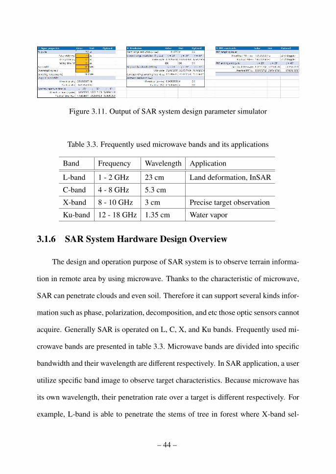
Figure 3.11. Output of SAR system design parameter simulator
Table 3.3. Frequently used microwave bands and its applications
Band Frequency Wavelength Application
L-band 1 - 2 GHz 23 cm Land deformation, InSAR
C-band 4 - 8 GHz 5.3 cm
X-band 8 - 10 GHz 3 cm Precise target observation
Ku-band 12 - 18 GHz 1.35 cm Water vapor
3.1.6 SAR System Hardware Design Overview
The design and operation purpose of SAR system is to observe terrain informa-
tion in remote area by using microwave. Thanks to the characteristic of microwave,
SAR can penetrate clouds and even soil. Therefore it can support several kinds infor-
mation such as phase, polarization, decomposition, and etc those optic sensors cannot
acquire. Generally SAR is operated on L, C, X, and Ku bands. Frequently used mi-
crowave bands are presented in table 3.3. Microwave bands are divided into specific
bandwidth and their wavelength are different respectively. In SAR application, a user
utilize specific band image to observe target characteristics. Because microwave has
its own wavelength, their penetration rate over a target is different respectively. For
example, L-band is able to penetrate the stems of tree in forest where X-band sel-
– 44 –
dom penetrates. However, due to the X-band microwave signal cannot penetrate the
small target it can acquire the surface information of target better than other lower
frequency bands. Therefore when designing SAR system designer should consider
the microwave bands according to user applications.
Platform stability and wavelength also should be considered when designing
operational mission because the position change during the mission can affect to
phase mismatch on receiving stage. In case of SAR system using L-band, it is easy
to operate mission on airplane because it has wavelength of 23 cm. X-band which
has the wavelength of 3 cm, however, can be easily affected from turbulence when it
is loaded on aircraft platform.
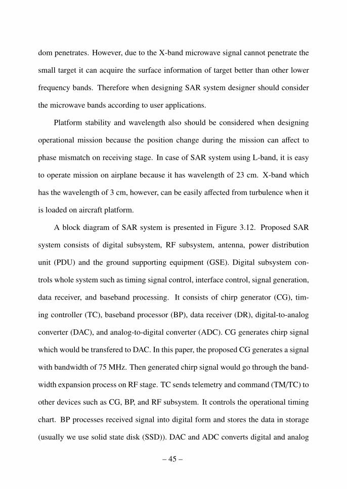
A block diagram of SAR system is presented in Figure 3.12. Proposed SAR
system consists of digital subsystem, RF subsystem, antenna, power distribution
unit (PDU) and the ground supporting equipment (GSE). Digital subsystem con-
trols whole system such as timing signal control, interface control, signal generation,
data receiver, and baseband processing. It consists of chirp generator (CG), tim-
ing controller (TC), baseband processor (BP), data receiver (DR), digital-to-analog
converter (DAC), and analog-to-digital converter (ADC). CG generates chirp signal
which would be transfered to DAC. In this paper, the proposed CG generates a signal
with bandwidth of 75 MHz. Then generated chirp signal would go through the band-
width expansion process on RF stage. TC sends telemetry and command (TM/TC) to
other devices such as CG, BP, and RF subsystem. It controls the operational timing
chart. BP processes received signal into digital form and stores the data in storage
(usually we use solid state disk (SSD)). DAC and ADC converts digital and analog
– 45 –
Imp
lemen
ted o
n F
PG
A b
oard
Baseb
and
pro
cessing
Chirp
signal
generation
Digital
to analog
conversi
on
FPGA RFBP CG DAC
Up-
conversi
on
HPA
Down-
conversi
on
LNA
Tx
Rx
Tx
ANT
Rx
ANT
Data
storage
SAR
controller
Sensors
Ethernet
EthernetEthernet
SMA SMA
SMA
LV
DS
IMU
GPS
PDUOBC
BP: Baseband processor
CG: Chirp generator
TC: Timing controller
PDU: Power distribution unit
OBC: Onboard computer
Analog
to digital
conversi
on
ADC
SMA
LV
DS
Timing
control
TC
Figure 3.12. Block diagram of SAR system
signal to be used in other subsystems.
RF subsystem consists of transmitter unit (Tx) and receiver unit (Rx). Tx unit
up-converts baseband signal to RF stage and the frequency multiplier unit expands
chirp signal by factor of 4. During this process the bandwidth of generated chirp sig-
nal is expanded to 300 MHz. Also, the solid stated power amplifier (SSPA) type high
power amplifier (HPA) inputs signal power and transfer the signal to transmission
antenna (Tx ANT). Tx ANT transmits observation signal which is generated from
Tx unit to the target in interest. On the receiving stage, receiver antenna (Rx ANT)
receives back-scattered signal from target. When designing radar system, generally,
a designer adopts Tx and Rx as one unit by using circulator. However the proposed
– 46 –

Pulse width
BandwidthSimulation
run
Chirp rate
Starting frequency
Input clk
Frequency accumulator
Phase accumulator
Sine LUT (Q)
Cosine LUT (I)
DAC Q data
ADC I data
ADC Q dataRAM
SSD memory on PC
Image processor
Antenna(Tx 1)
Frequency increment
Power
Transmitter
Receiver
PRF
Tx gate ctrl
Rx gate ctrlMTC
GNSS
IMU
Gigabit Ethernet
FPGA board
AD/DA cardDAC I data
JES
D204B
FM
C-H
PC
OBC
DDFS signal generator
AntennaRF part
Signal control
Reference clock
Antenna(Rx 1)
+28V/5A+28V/5A
+12V/5A
Baseband processor
AC/DC inverter
Power SMA Ethernet
Frequency generator
HUB
Gigabit Ethernet Gigabit Ethernet
DMA
Figure 3.13. Internal block diagram of UAV on-board X-band SAR System
SAR system uses Tx and Rx units respectively to utilize full-polarimetric function.
Rx unit receives signal from Rx ANT and down-converts RF signal into baseband
signal to be process in digital subsystem.
3.1.7 System Structure of SAR System
The system structure of the proposed X-band SAR system is presented in fig-
ure 3.13. Proposed SAR system consists of the chirp signal generator on the field pro-
grammable gate array (FPGA), digital-to-analog and analog-to-digital card (AD/DA
card), on-board computer (OBC), RF system, and antennas. The OBC unit consists
of the SAR system controller that controls operation and commands. Also, it equips
the IMU and GNSS units for attitude positioning. The FPGA unit consists of the
parallel DDS chirp signal generator, mode and timing controller (MTC), and base-
– 47 –

FM
C-H
PC
HPA
Mixer
LNAMixer
Hub
SAR Controller
3
4
5613_1
15_2
User GUI
22Tx I data
Tx Q data
Rx I data
Rx Q dataHPA
Mixer
13_2
LNAMixer
15_1
1
2
Tx/Rx Control
Software
14,16
RF systemFPGAOBC
Data Receiver
23
24
Signal processor and
displaying processor on MATLAB
27
17AC/DC
converter
AC input
: Ethernet interface
: Power : Clock signal input
: SMA cable
Figure 3.14. Block diagram of UAV on-board X-band SAR System
band processor (BP). The MTC defines the SAR observation modes and distributes
the commands to RF system such as the control signals for Tx and Rx window gates.
The BP stores the received signal from ADC to internal RAM unit and transmits the
8-bit digital data to OBC via PCIe 3.0 interface. RF unit consists of Tx and Rx parts,
frequency generator for up and down-conversion. As the X-band has high frequency,
the IF stage up-conversion in I & Q modulator and the RF stage up-conversion in the
high power amplifier (HPA) are considered.
In this section, Faraday rotation on linearly polarized SAR system is assumed
and the effect from Faraday rotation on image quality is investigated. Due to Fara-
day rotation, the reference plane of polarization rotates, then consequently it occurs
polarization mismatch on receiving stage. As SAR system forms its image using
– 48 –
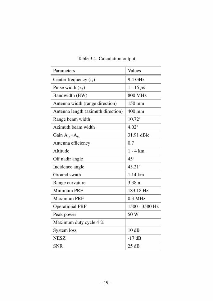
Table 3.4. Calculation output
Parameters Values
Center frequency (fc) 9.4 GHz
Pulse width (τp) 1 - 15 µs
Bandwidth (BW) 800 MHz
Antenna width (range direction) 150 mm
Antenna length (azimuth direction) 400 mm
Range beam width 10.72◦
Azimuth beam width 4.02◦
Gain Atx=Arx 31.91 dBic
Antenna efficiency 0.7
Altitude 1 - 4 km
Off nadir angle 45◦
Incidence angle 45.21◦
Ground swath 1.14 km
Range curvature 3.38 m
Minimum PRF 183.18 Hz
Maximum PRF 0.3 MHz
Operational PRF 1500 - 3580 Hz
Peak power 50 W
Maximum duty cycle 4 %
System loss 10 dB
NESZ -17 dB
SNR 25 dB
– 49 –
correlation operation, if there is error on received backscattered signal, the correla-
tion level will degrade. In L-band case, Faraday rotation occurs about 40° and this
increases the polarization mismatch. However, in circularly polarized SAR case, it
eliminates the polarization mismatch ideally. Simulation results show that CP mi-
crowave has better performance than LP in the respect of IRF characteristics. To
precisely verify the enhancement when using CP microwave, the simulation results
are needed to be investigated with actual SAR data.
– 50 –

Chapter 4. Design of DDS Chirp SignalGenerator on FPGA
There are several satellite on-board SAR systems those had and have been
launched and operated. Recently, Korea Aerospace Research Industry (KARI) has
launched Korea multi-purpose satellite-5 (KOMPSAT-5) in 2013 which is the first
Korean satellite on-board SAR [7]. Also, Japan Aerospace Exploration Agengy
(JAXA) has launched SAR equipped satellite named advanced land observing satellite-
2 (ALOS-2) in 2014. Other countries such as Germany and Italy are operating high-
resolution SAR systems such as Terra SAR-X and COSMO-SkyMed. Most of them
provide high-resolution SAR images (less than 1 m) using wide bandwidth chirp sig-
nal generators. For example, Terra SAR-X and COSMO-SkyMed use bandwidth of
300 MHz so that those satellites can provide the resolution of 0.5 m approximately.
The bandwidth of SAR has been increased up to 300 - 500 MHz to provide sub-meter
class resolution in military use.
As an imaging radar, SAR requires the wideband chirp signal to generate high-
resolution images because the resolution is inverse proportional to the signal band-
width. To provide the high-resolution SAR images, several kinds of chirp genera-
tion methods have been introduced. Representatively, the memory-map type gener-
ator and direct digital synthesizer (DDS) or the direct digital frequency synthesizer
(DDF) type generator exist. Generally these chirp generators are implemented on the
– 51 –
field programmable gate array (FPGA) or the application specific integrated circuit
(ASIC).
The memory-map based signal generator stores the pre-defined chirp waveform
in read-only memory (ROM) and reconstructs the waveform according to the system
clock [20, 42, 28]. The main feature of memory-map based signal generator is that it
supports near ideal time-domain signal output and spectrum. Usually, the memory-
map based signal generator in space mission generates narrow bandwidth signal in
baseband. Next, using the frequency multiplier, the baseband signal is up-converted
from baseband to IF and from IF to RF stages. On the up-conversion stage from IF
to RF, the bandwidth of output signal is expanded from tens of MHz to the hundreds
of MHz. The memory-map based signal generator with frequency multiplier has
been used on several satellites such as TerraSAR-X and COSMO-SkyMed. However,
the frequency multiplier has a disadvantage that it suffers phase noise because of
multiplying coefficients. Inter-modulation occurs within signals due to the DC offset
and image signal components of chirp. Also, memory-map based signal generator
requires a large size of memory when it is required to generate fine wide bandwidth
signal. In space environment memory unit is easily get damaged because of cosmic
ray therefore there is high risk when using memory-map based chirp generator for
wideband chirp generation.
Another type of frequently used chirp generator is DDS [28]. The memory-map
based signal generator requires large size of memory. Hence, especially in space
mission, the reconfiguration and data update take long time [8]. Therefore the DDS
signal generator has been proposed which can minimize the size of memory. DDS
– 52 –

consists of sets of register, counter, look-up table (LUT), and DAC. Compare to
the memory-map based signal generator, DDS stores only one cycle of amplitude
information of sinusoid in LUT. It can take the advantage of relatively small memory
size using LUT. The register and counter units called accumulator accumulate the
constant input signal in every clock rising time. Accumulator generates the phase
signal of desired waveform as digital data [43, 44, 20, 45].
There are some trade-offs between two representative chirp signal generators.
The memory-map based signal generator stores ideal chirp data so that the specrum
shows near-ideal characteristics. However, as the DDS suffers from truncation during
signal generation process, its spectrum characteristic shows non-ideal performance
due to the lack of expression bits. However, compare to the memory-map based
signal generator, DDS can easily control the frequency and phase by adjusting the
input and offset signals.
The bandwidth of baseband signal of both two generators are limited by the
specification of DAC and clock frequency due to the sampling theorem. To overcome
the limitation of the electronic devices such as clock frequency, the parallel DDS
(PDDS) has been implemented on recent SAR systems. It can support the ultra-
wideband using multiple DDS units and high-speed multiplexers. However, residual
noise of DDS remains and it degrades the spectrum purity of chirp signal. Therefore
this section proposes the error compensation algorithm for DDS type wideband chirp
signal generator.
Strong point of DDS signal generator is that it requires less memory than memory-
map based signal generator [?]. When radar system is operated in space orbit, mem-
– 53 –
ory unit is easily damaged, so the memory-map based chirp signal generator is con-
sidered to be replaced with next generation chirp signal generator. Also as the radar
system requires high-resolution output, a chirp signal generator should be able to
generate wide-bandwidth chirp signal. When the memory-map based chirp signal
generator generates the wide-bandwidth chirp signals, it requires large memory than
DDS chirp signal generator.
Even though DDS signal generator has been introduced to compensate the dis-
advantages of memory-map based chirp signal generator (e.g. memory dependabil-
ity, limitation of clock frequency, and etc.), DDS signal generator also has some weak
points. Representatively, the disadvantages of DDS signal generator are low spec-
trum purity due to the truncation error, phase shifting property, and etc. Main reason
that DDS chirp signal generator cannot be used in space mission is its low spectrum
property. However, if the phase error or low spectrum purity can be improved, DDS
chirp signal generator can replace the conventional memory-map based chirp signal
generator with low cost, low power consumption, and low design complexity.
In this chapter, the characteristics and phase error of DDS chirp signal generator
and the phase error compensation method will be discussed.
4.1 Conventional DDS Chirp Signal Generator
Compare to the conventional phase-lock loop (PLL) based frequency synthesiz-
ers, the DDSs have several advantages: the high-performance of frequency resolu-
tion, high-speed switching, low-phase noise, and etc [46].
– 54 –

LPF
LPF
90° phase shifter
Local OSC
HPA
Output
I data
Q data
DAC
DAC
DDFS(I data)
DDFS(Q data)
(a) (b) (c)
(d)
(e)
Clock LO
Figure 4.1. Simplified block diagram of transmission system
The main feature of DDS is that its structure is simple and it is easy to control
and reprogram. The amplitude of sinusoid has non-linear characteristic to the time,
however, it is easier to store and synthesize as digital data.
There are also the disadvantages of DDS. As the DDS regenerates the sinusoid
or chirp using digitized data, the phase noise occurs due to the discrete spur from the
external clock. Also, there is trade-off between wide bandwidth and high-spectrum
purity, hence it is hard to achieve the design goals.
4.1.1 Structure of Basic Radar System and Analysis on ErrorSources
When the signals pass through the DAC, low-pass-filter (LPF), mixer, and HPA,
it suffer from the several system noises. Figure 4.1 shows the simplified block dia-
gram of transmission system [40]. The error occurred during the signal transmission
procedure can be classified into five categories as depicted in the figure 4.1 and ta-
– 55 –
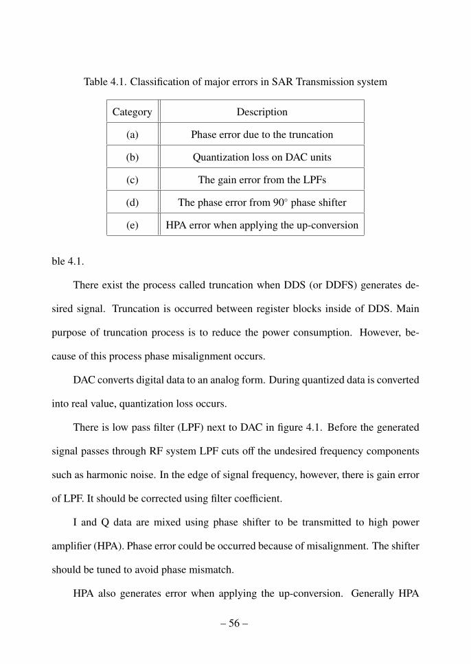
Table 4.1. Classification of major errors in SAR Transmission system
Category Description
(a) Phase error due to the truncation
(b) Quantization loss on DAC units
(c) The gain error from the LPFs
(d) The phase error from 90◦ phase shifter
(e) HPA error when applying the up-conversion
ble 4.1.
There exist the process called truncation when DDS (or DDFS) generates de-
sired signal. Truncation is occurred between register blocks inside of DDS. Main
purpose of truncation process is to reduce the power consumption. However, be-
cause of this process phase misalignment occurs.
DAC converts digital data to an analog form. During quantized data is converted
into real value, quantization loss occurs.
There is low pass filter (LPF) next to DAC in figure 4.1. Before the generated
signal passes through RF system LPF cuts off the undesired frequency components
such as harmonic noise. In the edge of signal frequency, however, there is gain error
of LPF. It should be corrected using filter coefficient.
I and Q data are mixed using phase shifter to be transmitted to high power
amplifier (HPA). Phase error could be occurred because of misalignment. The shifter
should be tuned to avoid phase mismatch.
HPA also generates error when applying the up-conversion. Generally HPA
– 56 –
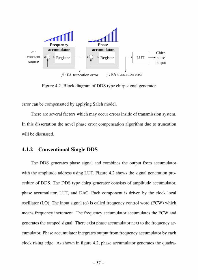
Register++ Register+
+ LUT
α :
constant
source
β : FA truncation error γ : PA truncation error
Chirp
pulse
output
Frequency
accumulator
Phase
accumulator
Figure 4.2. Block diagram of DDS type chirp signal generator
error can be compensated by applying Saleh model.
There are several factors which may occur errors inside of transmission system.
In this dissertation the novel phase error compensation algorithm due to truncation
will be discussed.
4.1.2 Conventional Single DDS
The DDS generates phase signal and combines the output from accumulator
with the amplitude address using LUT. Figure 4.2 shows the signal generation pro-
cedure of DDS. The DDS type chirp generator consists of amplitude accumulator,
phase accumulator, LUT, and DAC. Each component is driven by the clock local
oscillator (LO). The input signal (α) is called frequency control word (FCW) which
means frequency increment. The frequency accumulator accumulates the FCW and
generates the ramped signal. There exist phase accumulator next to the frequency ac-
cumulator. Phase accumulator integrates output from frequency accumulator by each
clock rising edge. As shown in figure 4.2, phase accumulator generates the quadra-
– 57 –

ture polynomial output because the phase of chirp signal is in quadrature form. LUT
contains the amplitude information of the one cycle of sinusoid. Using the output
from phase accumulator it generates desired chirp signal. The mathematical expres-
sion of the baseband ideal chirp in time domain is shown as
s (t) = rect(
tT
)exp
{jπKt2
}
= rect(
tT
) {cos
(πKt2
)+ j sin
(πKt2
)},
(4.1)
where t, T, and K indicates the time variable, the pulse width, and the chirp rate
respectively. The envelope of (??), rect function, can be defined as
rect( tT
)= 1,where − T/2 ≤ t ≤ T/2. (4.2)
From (4.1), it is shown that the phase of chirp signal has the form of quadratic poly-
nomial. To investigate the phase and frequency components of chirp signal, (4.3) and
(4.4) are shown as
φ (t) = πKt2, (4.3)
f (t) =1
2πdφ (t)
dt= Kt. (4.4)
From (4.4), the instantaneous frequency f (t) varies with the rate K within a time t,
therefore the chirp signal sweeps through the bandwidth Kt [Hz]. Considering that
DDS is digital system, the chirp signal generator operates in discrete manner. In
this dissertation, we consider that the system is N-bit long. When expressing the
clock frequency as fclk, the frequency increment and output frequency of DDS can
– 58 –
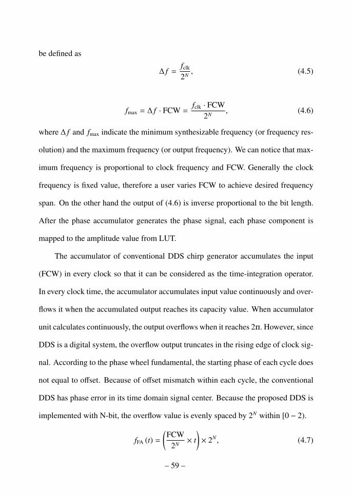
be defined as
∆ f =fclk
2N , (4.5)
fmax = ∆ f · FCW =fclk · FCW
2N , (4.6)
where ∆ f and fmax indicate the minimum synthesizable frequency (or frequency res-
olution) and the maximum frequency (or output frequency). We can notice that max-
imum frequency is proportional to clock frequency and FCW. Generally the clock
frequency is fixed value, therefore a user varies FCW to achieve desired frequency
span. On the other hand the output of (4.6) is inverse proportional to the bit length.
After the phase accumulator generates the phase signal, each phase component is
mapped to the amplitude value from LUT.
The accumulator of conventional DDS chirp generator accumulates the input
(FCW) in every clock so that it can be considered as the time-integration operator.
In every clock time, the accumulator accumulates input value continuously and over-
flows it when the accumulated output reaches its capacity value. When accumulator
unit calculates continuously, the output overflows when it reaches 2π. However, since
DDS is a digital system, the overflow output truncates in the rising edge of clock sig-
nal. According to the phase wheel fundamental, the starting phase of each cycle does
not equal to offset. Because of offset mismatch within each cycle, the conventional
DDS has phase error in its time domain signal center. Because the proposed DDS is
implemented with N-bit, the overflow value is evenly spaced by 2N within [0 − 2).
fFA (t) =
(FCW
2N × t)× 2N , (4.7)
– 59 –
φPA (t) =
12
(FCW
2N × t)2
×2N
2p
, (4.8)
where fFA (t), φPA (t), and p are the output from frequency and phase accumulators,
and p-truncated bit respectively.
4.1.3 Description of Parallel DDS
The common problem of the memory-map based type and DDS is that both two
signal generators are limited their output bandwidth due to the main clock frequency.
Especially, in the case of space mission, the available clock frequency is very limited.
The bandwidth of conventional DDS has limitation of clock frequency. To satisfy
the Nyquist’s theorem, the sampling frequency should be larger then two times of
signal bandwidth. Also, to acquire the stable signal, [1] suggests to use the sampling
frequency of four times larger than the bandwidth. In this case, if the clock frequency
is not sufficient, it would ba a hard task to generate the wideband signal.
To overcome the clock frequency problem, the parallel DDS has been pro-
posed [38, 47, 48]. Most cases, it has 4-DDS in parallel and 4:1 multiplexer (MUX)
combines the output signal from each LUT. The block diagram of parallel DDS is
shown in figure 4.3. PDDS consists of one set of frequency accumulator and phase
accumulator, four LUTs, and 4:1 MUX. The operational structure of DDS in fig-
ure 4.3 is same with figure 4.3. The main difference from the conventional one is that
the parallel DDS operates as sequential manner. The output frequency of parallel
– 60 –
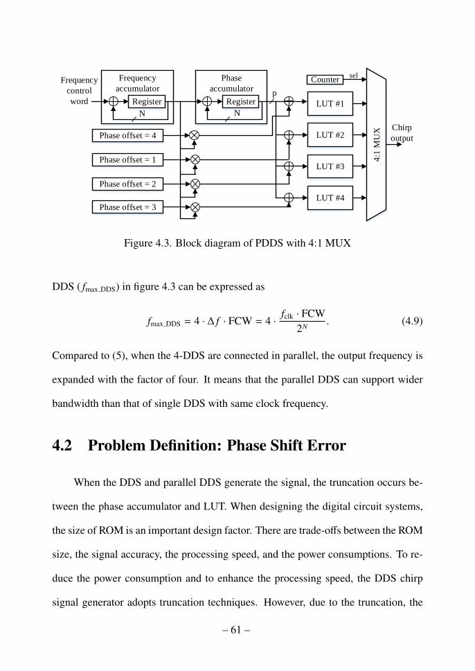
Phase
accumulator
Register
Frequency
accumulator
Register LUT #1
Phase offset = 4
Phase offset = 1
Phase offset = 2
Phase offset = 3
LUT #2
LUT #3
LUT #4
4:1
MU
X
Countersel
N N
p
Frequency
control
word
Chirp
output
Figure 4.3. Block diagram of PDDS with 4:1 MUX
DDS ( fmax DDS) in figure 4.3 can be expressed as
fmax DDS = 4 · ∆ f · FCW = 4 ·fclk · FCW
2N . (4.9)
Compared to (5), when the 4-DDS are connected in parallel, the output frequency is
expanded with the factor of four. It means that the parallel DDS can support wider
bandwidth than that of single DDS with same clock frequency.
4.2 Problem Definition: Phase Shift Error
When the DDS and parallel DDS generate the signal, the truncation occurs be-
tween the phase accumulator and LUT. When designing the digital circuit systems,
the size of ROM is an important design factor. There are trade-offs between the ROM
size, the signal accuracy, the processing speed, and the power consumptions. To re-
duce the power consumption and to enhance the processing speed, the DDS chirp
signal generator adopts truncation techniques. However, due to the truncation, the
– 61 –

Phase Accumulator
RegisterN
p p-bit LUT
N-bit output
p-bit MSB from N-bit line
: N-bit line: p-bit line
Figure 4.4. N-bit truncation between phase accumulator and LUT
accuracy of DDS degrades. Figure 4.4 shows the truncation process between phase
accumulator and LUT [49, 50]. We assume that every single component inside of
DDS except LUT is calculated with N-bit long data. However LUT stores ampli-
tude data with p-bit. In this case, the N-bit long output from phase accumulator is
truncated to p-bit. LUT uses only p-bit most significant bit (MSB) from phase accu-
mulator. In this dissertation we assume that N = 16. However, when the N-bit output
in truncated, the truncation causes the loss of expression bits and consequently the
output of DDS suffers from the truncation noise.
Figure 4.5 shows the real part of chirp signal waveform in time domain of ideal
signal and conventional DDS. Generated signals are 3.6 µs long respectively and
magnified in the center. The solid line and dashed line represent the ideal signal and
the conventional DDS signal respectively. Chirp signal consists of real and imaginary
parts respectively as shown in (4.1). Real part of chirp has cosine wave term and
imaginary part has sine wave term. It indicates that the real part signal in time domain
should have cosine form. In figure 4.5, the ideal chirp waveform (solid line) shows
– 62 –
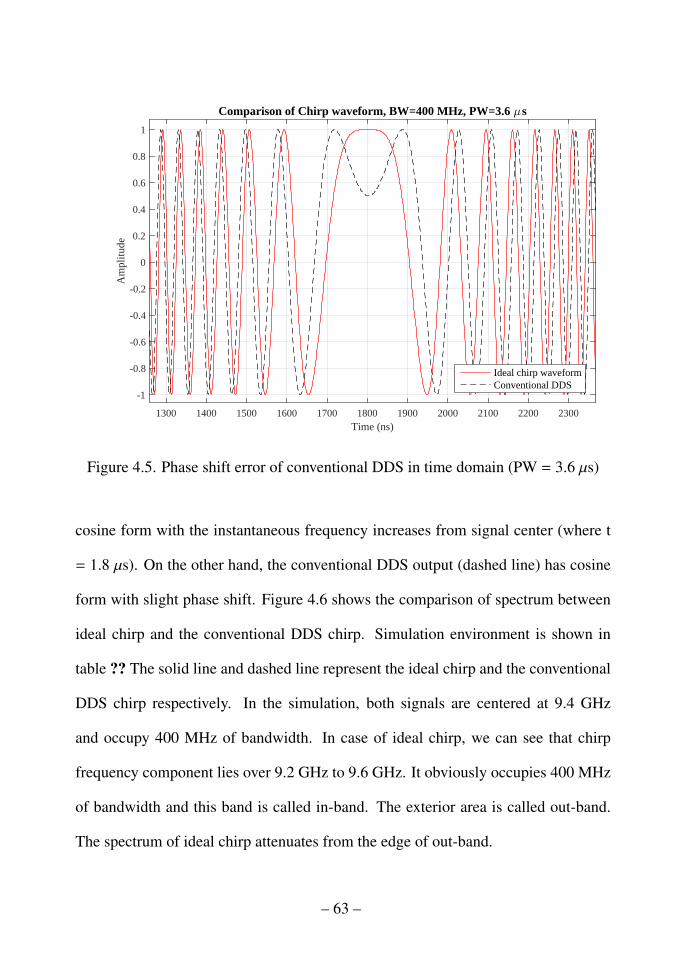
Time (ns)1300 1400 1500 1600 1700 1800 1900 2000 2100 2200 2300
Am
plitu
de
-1
-0.8
-0.6
-0.4
-0.2
0
0.2
0.4
0.6
0.8
1
Comparison of Chirp waveform, BW=400 MHz, PW=3.6 7s
Ideal chirp waveformConventional DDS
Figure 4.5. Phase shift error of conventional DDS in time domain (PW = 3.6 µs)
cosine form with the instantaneous frequency increases from signal center (where t
= 1.8 µs). On the other hand, the conventional DDS output (dashed line) has cosine
form with slight phase shift. Figure 4.6 shows the comparison of spectrum between
ideal chirp and the conventional DDS chirp. Simulation environment is shown in
table ?? The solid line and dashed line represent the ideal chirp and the conventional
DDS chirp respectively. In the simulation, both signals are centered at 9.4 GHz
and occupy 400 MHz of bandwidth. In case of ideal chirp, we can see that chirp
frequency component lies over 9.2 GHz to 9.6 GHz. It obviously occupies 400 MHz
of bandwidth and this band is called in-band. The exterior area is called out-band.
The spectrum of ideal chirp attenuates from the edge of out-band.
– 63 –

Frequency [Hz] #1098.8 9 9.2 9.4 9.6 9.8 10
Pow
er [
dB]
-70
-60
-50
-40
-30
-20
-10
0
Comparison of Spectrum, BW = 400 MHz, PW = 3.6 7s
Ideal chirp waveformConventional DDS
Figure 4.6. Comparison of spectrum between ideal chirp and conventional DDS chirp
(BW = 400 MHz @ 9.4 GHz)
Dashed line, the spectrum of conventional DDS, also occupies 400 MHz of
bandwidth. Compare to ideal signal in in-band, however, the flatness of conventional
DDS spectrum is not firm. Moreover, out-band signal shows the spectral regrowth
components which is one of spurious.
In case of spectrum at 9 GHz, ideal chirp and conventional chirp have the ampli-
tude difference more than 8 dB. Those spurious components remain in whole system
and gets larger by passing other subsystems such as RF system and antenna. To
assure that DDS chirp generator can be used in SAR system, the phase shift error
should be compensated.
– 64 –
Parameters Value
Center frequency 9.4 GHz (X-band)
Pulse width 3.6 µs
Bandwidth ±200 MHz from center frequency
HPA type Solid state power amplifier (SSPA)
Integrated phase noise -60 dBc
Phase noise floor -120 dBc/Hz
4.3 Proposed Method
The proposed algorithm has two main features. First, it applies the curve fitting
method. Second, it calculate the error compensation coefficient, then compensates
error on each accumulator block.
4.3.1 Error Modeling Using Polynomial
During signal generation stage, each accumulator in DDS occurs residual offset
error because of the roll-over in every overflow cycle. We denote the residual error
components of the frequency and phase accumulators as and respectively. Using Eq.
(6) and Eq. (7), the output model of each accumulator can be expanded as
fFA (t) =
(FCW
2N × t)× 2N + fx, (4.10)
φPA (t) =
12
(FCW
2N × t)2
+
(fx
2N × t)
+φx
2N
× 2N
2p . (4.11)
This dissertation denotes the phase error of DDS (φerror (t)) as
φerror (t) =
{φ (t) −
φPA (t)(2N/2p)
}. (4.12)
– 65 –

To model the error from phase accumulator, we apply the curve fitting process on the
DDS phase error (φerror (t)) using 2nd order polynomial (φcf (t)) shown as
φcf (t) = αt2 + βt + γ, (4.13)
where α, β, and γ indicate the quadrature, linear, and random error coefficients of
conventional DDS respectively. The coefficients above will be used to compensate
the residual error from DDS components.
4.3.2 Error Compensation Using Coefficients
The compensated phase output of DDS (φcomp (t)) using proposed algorithm can
be expressed as
φcomp (t) =φPA(t)
(2N/2p) + φcf (t)
=φPA(t)
(2N/2p) +
{φ (t) − φPA(t)
(2N/2p)
}.
(4.14)
From Eq. 4.10 and Eq. 4.12, we can assure that the phase output of the proposed
method theoretically compensates the error. After extracting the error compensation
coefficients, we design the block diagram of the proposed error compensation algo-
rithm. Figure 4.7 shows that the phase output of DDS is processed with curve fitting
to generate 2nd order polynomial model. Next, the ideal phase of chirp generated
DDS IP core subtracts its signal with the DDS phase output. Last, we estimate the
error compensation coefficients, then calculates the quadrature, linear, and random
errors respectively. By differentiating , we divide each compensation coefficient ac-
cording to the signal generation process of DDS. 2α, β, andγ compensate FCW error,
the residual error of frequency and phase accumulators respectively.
– 66 –
Phase
accumulator
Register
Frequency
accumulator
RegisterFCW
Curve
fittingIdeal phase
generation using
DDFS IP core
Coefficient
estimation
LUT
2
2
ideal K 2 / 2N pt t 2
cf t t t
Figure 4.7. Block diagram of the proposed error compensation algorithm
4.4 Performance Analysis
In this section, the impulse response function (IRF) and spectrum output com-
parison are analyzed to verify the feasibility of the proposed error compensation
algorithm. In addition, we conduct the point target analysis simulation to verify the
effect of phase error and proposed method on SAR image.
4.4.1 Simulation and Experiment Environment
To validate the proposed error compensation algorithm, we implement DDS
and PDDS chirp signal generator on FPGA. The devices used in this dissertation is
shown in table 4.2 and table 4.3. We used two FPGA boards which are from Xilinx
and Microsemi. Each board has one clock input port and four signal output ports
(I+, I-, Q+, and Q-). Several times of simulation have been conducted on L-band and
X-band case.
– 67 –
Table 4.2. Description of FPGA board #1 (Xilinx) used in this dissertation
Parameters Value
FPGA vendor Xilinx
FPGA chip Virtex-5 XC5VLX50T-FFG1136C-1
Power source +6 V (DAC #1), +5 V (DAC #2)+3.3 V (FPGA)
Interface LVDS, SERDES, SMA
Input clock speed 150 MHz
DAC #1 AD9731 (Analog Device)
DAC #1 sampling speed 170 MSPS
DAC #1 bit resolution 10 bit
DAC #2 EV12DS130AGS (e2v)
DAC #2 sampling speed 3GSPS
DAC #2 bit resolution 12 bit
DAC #2 MUX 2:1, 4:1 selectable
Table 4.3. Description of FPGA board #2 (Microsemi) used in this dissertation
Parameters Value
FPGA vendor Microsemi
FPGA chip RT4G1501657PROTO
Power source +5 V (DAC), +3.3 V (FPGA)
Interface LVDS, SpW, SMA (Clk in), SMC (signal out)
Input clock speed 600 MHz (internal divider divides clock down to 300 MHz)
DAC EV12DS130AGS (e2v)
DAC sampling speed 3GSPS
DAC bit resolution 12 bit
DAC MUX 2:1, 4:1 selectable
– 68 –

4.4.2 Comparison of Impulse Response Function and Spectrum
We investigate the peak-to-side lobe ratio (PSLR) and the integrated side lobe
ratio (ISLR) from IRF. PSLR indicates the noise level between peak and side lobe.
ISLR presents the proportion of energy between the main lobe and the side lobe from
the first to 10th nulls on both side.
To evaluate the performance of the proposed PDDS chirp signal generator using
phase error compensation block, we build the PDDS simulation block using VHDL.
In simulation, the conventional PDDS chirp signal generator is modeled with 4 DDS
blocks. The conventional PDDS and the proposed PDDS generate the chirp signal
simultaneously with the same simulation parameters. In simulation, only I data of
chirp signal is considered.
Also, we adapt Chebyshev filter as LPF to eliminate the undesired harmon-
ics. We design a 5-th order low-pass Chebyshev Type-1 filter with 0.1 dB ripple
in passband and a normalized passband edge frequency value of 0.9 to meet the re-
quirements when designing chirp signal generator. Each I and Q data is divided, then
filtered with the low-pass filter we designed. First, we compare the chirp signal out-
put of ideal signal, conventional PDDS signal and the proposed PDDS signal in time
domain to verify that the proposed phase error compensation method can mitigate
the phase shifting occurred from truncation error. In simulation, the proposed PDDS
signal traces the ideal chirp signal. Figure 4.8 presents the I data of ideal signal,
conventional PDDS signal , and the proposed PDDS chirp signal, respectively. In the
signal center, the conventional PDDS still has the shifted phase components, however
– 69 –

1400 1500 1600 1700 1800 1900 2000 2100 2200−1
−0.8
−0.6
−0.4
−0.2
0
0.2
0.4
0.6
0.8
1
time(µs)
ampl
itude
Ideal chirp waveformConv. PDDS chirp waveformProposed PDDS chirp waveform
Figure 4.8. Comparison between time domain chirp signals.
the proposed PDDS signal has the signal plot identical to ideal chirp waveform.
As shown in Figure 4.9, the conventional PDDS chirp signal generator has the
phase error of -4,000 in the center of signal. However, it is shown that the phase
signal of proposed PDDS traces ideal signal phase. This result shows that phase
error can be compensated by adjusting the frequency offset.
Figure 4.10 and figure 4.11 show the IRF and spectrum output of the conven-
tional DDS and the proposed method respectively. For the simulation, 400 MHz of
chirp with 3.6 µs pulse width which is centered in 9.4 GHz has been generated. In
both figures, the dashed line and the solid line indicate the graph of conventional
DDS and the proposed method output respectively. The mathematical expressions of
– 70 –

1650 1700 1750 1800 1850 1900 1950 2000−6000
−4000
−2000
0
2000
4000
6000
8000
time(µs)
ampl
itude
Ideal signal phasePDDS signal phaseProposed PDDS phase
Figure 4.9. Comparison of phase signal between chirp signals.
PSLR and ISLR are presented as
IPSLR = Imain[dB] − Ix[dB], (4.15)
IISLR =
∫ 1N
−1N|h (t)|2dt∫ −10N
−1N|h (t)|2dt +
∫ 10N
N|h (t)|2dt
, (4.16)
where Imain and Ix are the peak value of main-lobe and side-lobe [?]. From Fig. ??
(a), the conventional DDS shows -13.3920 dB of PSLR and -10.0857 dB of ISLR.
On the other hand, the DDS using proposed method shows higher PSLR and ISLR;
-13.5688 dB and -10.1948 dB respectively. It means that IRF performance has been
enhanced when using the proposed method. Table. 4.4 shows the comparison of IRF
output between the conventional and proposed DDS. We evaluate the chirp signals
– 71 –

Time (7s)1740 1760 1780 1800 1820 1840 1860
Am
plitu
de (
dB)
-30
-25
-20
-15
-10
-5
0Comparison of IRF in dB unit, BW=400 MHz, PW=3.6 7s
Conventional DDS, PSLR=-13.392, ISLR=-10.0857Proposed DDS, PSLR=-13.5668, ISLR=-10.1948
Figure 4.10. IRF output comparison
in frequency domain to compare the spectral regrowth and purity. In this simula-
tion, frequency domain signals are considered and to present the signals in dB scale,
signals are modified with formula as follow. It is assumed that all the signal is up-
converted from baseband to RF stage (1.27GHz) by RF carrier source. First, we take
the fast Fourier transform (FFT) to convert the signal from time domain to frequency
domain. The dB scale signal is defined as [51]
sideal dB ( f ) = 20log10|sideal ( f )||sideal ( f )|max
. (4.17)
where sideal dB( f ) indicates dB scale signal of ideal chirp signal generator.
To verify the signal characteristics of proposed PDDS chirp signal generator,
we modeled the RF systems in simulation. Simulation parameters of RF system are
– 72 –

Frequency [Hz]#109
8.9 9 9.1 9.2 9.3 9.4 9.5 9.6 9.7 9.8 9.9
Pow
er [
dB]
-60
-50
-40
-30
-20
-10
Comparison of Spectrum in RF impairments, BW=400 MHz, PW=3.6 7s
Conventional DDSProposed DDS
Figure 4.11. Spectrum comparison
shown in Table 4.5. In simulation, to enhance the resolution of results, a zero padding
technique is used on ideal signal, the conventional PDDS signal, and the proposed
PDDS signal, respectively.
Figure 4.12 shows the spectrum plot of conventional PDDS and the proposed
PDDS. Within the passband (1.27 GHz ± 144 MHz), the spectrum of conventional
PDDS and the proposed method overlap each other. However, the ripple of the pro-
posed method in passband is smaller than that of conventional PDDS. In noise band,
the spectrum of both conventional PDDS and the proposed method attenuates. In
Figure 4.12, the spectrum of the proposed method in noise band is reduced remark-
ably. As the SNR is the proportion between passband and noise band, it is shown
that the SNR of the proposed method is better than that of conventional PDDS.
– 73 –
Table 4.4. Result of IRF analysis
Parameters Conventional DDS Proposed method Enhancement
PSLR -13.3920 dB -13.5688 dB -0.2068 dB
ISLR -10.0857 dB -10.1948 dB -0.1091 dB
Table 4.5. Simulation parameters for RF system evaluation.
Parameters Features Unit
Cut-off frequency of PSD 10×103 Hz
Integrated phase noise -60 dBc
Phase noise floor -120 dBc/Hz
Sampling frequency 2,400 MHz
Amplitude imbalance 0.1 -
Phase imbalance 5.8 × π/180 -
In order to analyze the performance of the proposed phase error compensation
method, the PSLR and ISLR are investigated at a pulse repetition frequency at 2200
Hz.
A comparison of spectrum output is shown in figure 4.11. As shown in fig-
ure 4.11, the conventional DDS shows spurs. However, the solid line in figure 4.11
shows stable output compared to the conventional DDS output. We can assure that
the proposed error compensation algorithm is able to reduce spur components in
noise band.
– 74 –

0 0.5 1 1.5 2 2.5
x 109
−100
−90
−80
−70
−60
−50
−40
−30
−20
−10
0
frequency[Hz]
pow
er[d
B]
Conv. PDDS chirp waveformProposed PDDS chirp waveform
Figure 4.12. Comparison of dB scale chirp signal plots with RF impairments
4.4.3 Point target analysis
To verify the feasibility of proposed algorithm, this dissertation conducts point
target analysis using the chirp from conventional DDS and the proposed DDS. In
this simulation, we have one target in the center of interested area. The point target
images are processed using the range Doppler algorithm (RDA) and the range cell
migration (RCM) has been compensated. In addition, zero padding has been applied
to obtain clear images.
Fig. 4.13 shows the point target analysis results. Fig. 4.13 (a) and (b) are the
point target images when using the conventional DDS and the proposed DDS re-
spectively. In both figures, the 2-dimensional point targets are shown along range
– 75 –
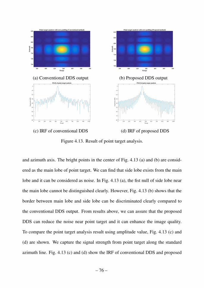
Point target analysis with zero padding (Conventional method)
Range380 400 420 440 460 480 500
Azi
mut
h640
660
680
700
720
740
760
(a) Conventional DDS output
Point target analysis with zero padding (Proposed method)
Range380 400 420 440 460 480 500
Azi
mut
h
640
660
680
700
720
740
760
(b) Proposed DDS output
Range0 100 200 300 400 500 600 700 800 900 1000
Am
plitu
de [
dB]
-80
-70
-60
-50
-40
-30
-20
-10
0
PSLR of point target analysis
(c) IRF of conventional DDS
Range0 100 200 300 400 500 600 700 800 900 1000
Am
plitu
de [
dB]
-80
-70
-60
-50
-40
-30
-20
-10
0
PSLR of point target analysis
(d) IRF of proposed DDS
Figure 4.13. Result of point target analysis.
and azimuth axis. The bright points in the center of Fig. 4.13 (a) and (b) are consid-
ered as the main lobe of point target. We can find that side lobe exists from the main
lobe and it can be considered as noise. In Fig. 4.13 (a), the fist null of side lobe near
the main lobe cannot be distinguished clearly. However, Fig. 4.13 (b) shows that the
border between main lobe and side lobe can be discriminated clearly compared to
the conventional DDS output. From results above, we can assure that the proposed
DDS can reduce the noise near point target and it can enhance the image quality.
To compare the point target analysis result using amplitude value, Fig. 4.13 (c) and
(d) are shown. We capture the signal strength from point target along the standard
azimuth line. Fig. 4.13 (c) and (d) show the IRF of conventional DDS and proposed
– 76 –
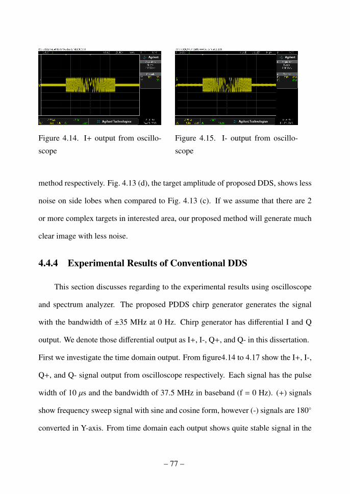
Figure 4.14. I+ output from oscillo-
scope
Figure 4.15. I- output from oscillo-
scope
method respectively. Fig. 4.13 (d), the target amplitude of proposed DDS, shows less
noise on side lobes when compared to Fig. 4.13 (c). If we assume that there are 2
or more complex targets in interested area, our proposed method will generate much
clear image with less noise.
4.4.4 Experimental Results of Conventional DDS
This section discusses regarding to the experimental results using oscilloscope
and spectrum analyzer. The proposed PDDS chirp generator generates the signal
with the bandwidth of ±35 MHz at 0 Hz. Chirp generator has differential I and Q
output. We denote those differential output as I+, I-, Q+, and Q- in this dissertation.
First we investigate the time domain output. From figure4.14 to 4.17 show the I+, I-,
Q+, and Q- signal output from oscilloscope respectively. Each signal has the pulse
width of 10 µs and the bandwidth of 37.5 MHz in baseband (f = 0 Hz). (+) signals
show frequency sweep signal with sine and cosine form, however (-) signals are 180◦
converted in Y-axis. From time domain each output shows quite stable signal in the
– 77 –
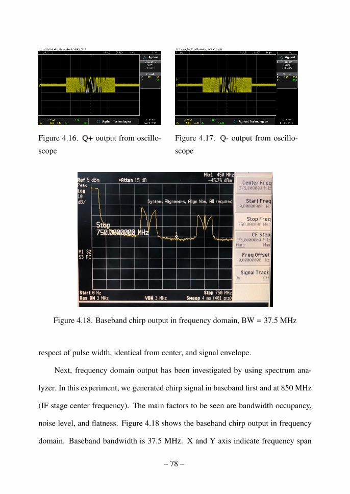
Figure 4.16. Q+ output from oscillo-
scope
Figure 4.17. Q- output from oscillo-
scope
Figure 4.18. Baseband chirp output in frequency domain, BW = 37.5 MHz
respect of pulse width, identical from center, and signal envelope.
Next, frequency domain output has been investigated by using spectrum ana-
lyzer. In this experiment, we generated chirp signal in baseband first and at 850 MHz
(IF stage center frequency). The main factors to be seen are bandwidth occupancy,
noise level, and flatness. Figure 4.18 shows the baseband chirp output in frequency
domain. Baseband bandwidth is 37.5 MHz. X and Y axis indicate frequency span
– 78 –
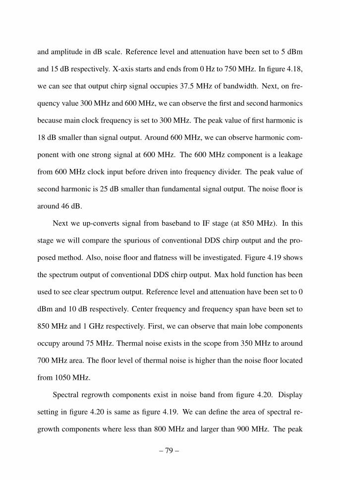
and amplitude in dB scale. Reference level and attenuation have been set to 5 dBm
and 15 dB respectively. X-axis starts and ends from 0 Hz to 750 MHz. In figure 4.18,
we can see that output chirp signal occupies 37.5 MHz of bandwidth. Next, on fre-
quency value 300 MHz and 600 MHz, we can observe the first and second harmonics
because main clock frequency is set to 300 MHz. The peak value of first harmonic is
18 dB smaller than signal output. Around 600 MHz, we can observe harmonic com-
ponent with one strong signal at 600 MHz. The 600 MHz component is a leakage
from 600 MHz clock input before driven into frequency divider. The peak value of
second harmonic is 25 dB smaller than fundamental signal output. The noise floor is
around 46 dB.
Next we up-converts signal from baseband to IF stage (at 850 MHz). In this
stage we will compare the spurious of conventional DDS chirp output and the pro-
posed method. Also, noise floor and flatness will be investigated. Figure 4.19 shows
the spectrum output of conventional DDS chirp output. Max hold function has been
used to see clear spectrum output. Reference level and attenuation have been set to 0
dBm and 10 dB respectively. Center frequency and frequency span have been set to
850 MHz and 1 GHz respectively. First, we can observe that main lobe components
occupy around 75 MHz. Thermal noise exists in the scope from 350 MHz to around
700 MHz area. The floor level of thermal noise is higher than the noise floor located
from 1050 MHz.
Spectral regrowth components exist in noise band from figure 4.20. Display
setting in figure 4.20 is same as figure 4.19. We can define the area of spectral re-
growth components where less than 800 MHz and larger than 900 MHz. The peak
– 79 –

Figure 4.19. Conventional DDS output in frequency domain
value of spectral regrowth in left side of chirp is approximately -22.37 dBm at 740
MHz. The level difference between signal center (850 MHz) and the peak spectral
regrowth is -30.56 dB as shown in figure 4.21. The minimum signal level difference
in the left side of chirp is shown in figure ?? and the value is -35.29 dB. In figure 4.23
and figure 4.24, the signal level differences in the right side of chirp are presented.
The maximum and minimum spectral growth level from 850 MHz to 960 MHz are
-38.97 dB and -35.35 dB respectively. Figure 4.25 presents the spectrum of conven-
tional DDS output where the reference level and attenuation level are 10 dBm and 20
dB respectively. We can observe the entire spectrum output where center frequency
and span are 850 MHz and 1 GHz respectively. Next, we investigate the flatness of
the chirp output of conventional DDS. Flatness indicates the spectrum purity within
– 80 –
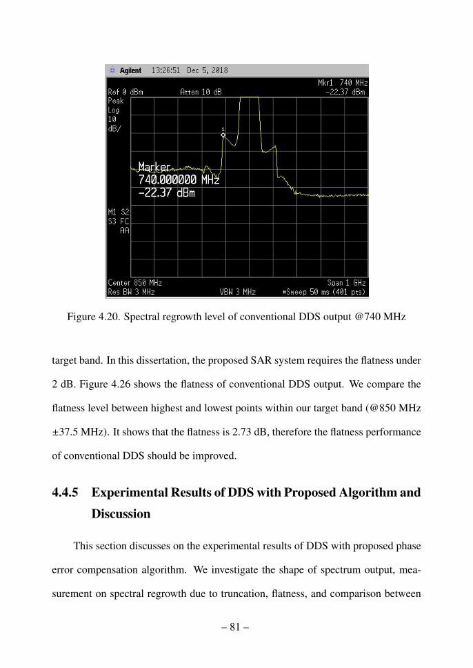
Figure 4.20. Spectral regrowth level of conventional DDS output @740 MHz
target band. In this dissertation, the proposed SAR system requires the flatness under
2 dB. Figure 4.26 shows the flatness of conventional DDS output. We compare the
flatness level between highest and lowest points within our target band (@850 MHz
±37.5 MHz). It shows that the flatness is 2.73 dB, therefore the flatness performance
of conventional DDS should be improved.
4.4.5 Experimental Results of DDS with Proposed Algorithm andDiscussion
This section discusses on the experimental results of DDS with proposed phase
error compensation algorithm. We investigate the shape of spectrum output, mea-
surement on spectral regrowth due to truncation, flatness, and comparison between
– 81 –
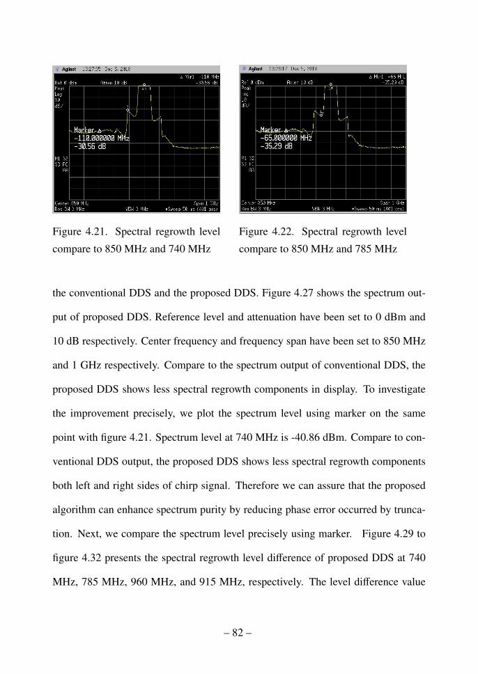
Figure 4.21. Spectral regrowth level
compare to 850 MHz and 740 MHz
Figure 4.22. Spectral regrowth level
compare to 850 MHz and 785 MHz
the conventional DDS and the proposed DDS. Figure 4.27 shows the spectrum out-
put of proposed DDS. Reference level and attenuation have been set to 0 dBm and
10 dB respectively. Center frequency and frequency span have been set to 850 MHz
and 1 GHz respectively. Compare to the spectrum output of conventional DDS, the
proposed DDS shows less spectral regrowth components in display. To investigate
the improvement precisely, we plot the spectrum level using marker on the same
point with figure 4.21. Spectrum level at 740 MHz is -40.86 dBm. Compare to con-
ventional DDS output, the proposed DDS shows less spectral regrowth components
both left and right sides of chirp signal. Therefore we can assure that the proposed
algorithm can enhance spectrum purity by reducing phase error occurred by trunca-
tion. Next, we compare the spectrum level precisely using marker. Figure 4.29 to
figure 4.32 presents the spectral regrowth level difference of proposed DDS at 740
MHz, 785 MHz, 960 MHz, and 915 MHz, respectively. The level difference value
– 82 –
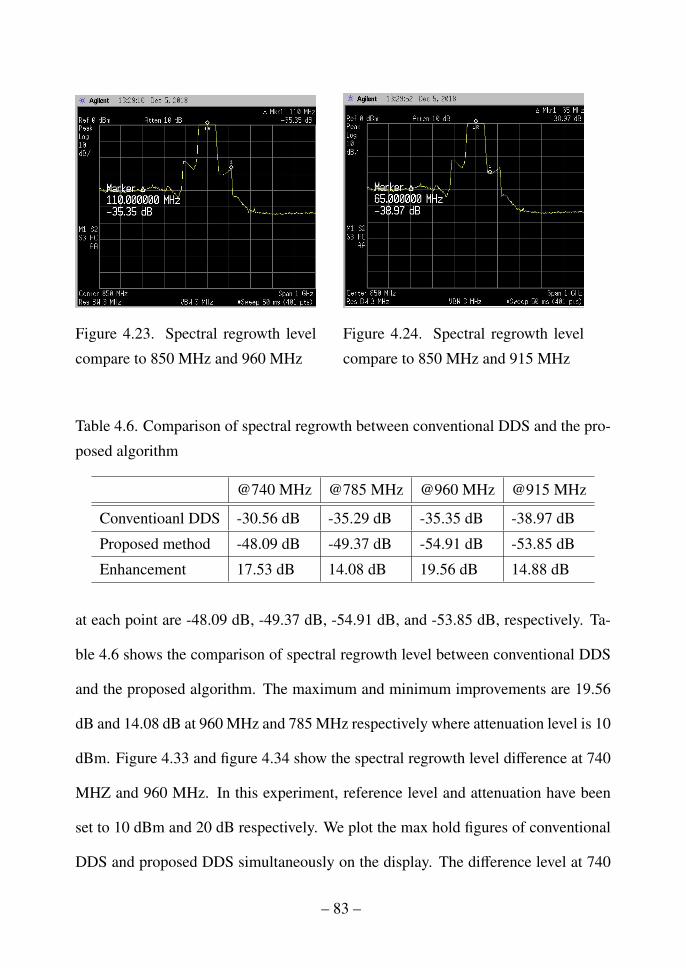
Figure 4.23. Spectral regrowth level
compare to 850 MHz and 960 MHz
Figure 4.24. Spectral regrowth level
compare to 850 MHz and 915 MHz
Table 4.6. Comparison of spectral regrowth between conventional DDS and the pro-
posed algorithm
@740 MHz @785 MHz @960 MHz @915 MHz
Conventioanl DDS -30.56 dB -35.29 dB -35.35 dB -38.97 dB
Proposed method -48.09 dB -49.37 dB -54.91 dB -53.85 dB
Enhancement 17.53 dB 14.08 dB 19.56 dB 14.88 dB
at each point are -48.09 dB, -49.37 dB, -54.91 dB, and -53.85 dB, respectively. Ta-
ble 4.6 shows the comparison of spectral regrowth level between conventional DDS
and the proposed algorithm. The maximum and minimum improvements are 19.56
dB and 14.08 dB at 960 MHz and 785 MHz respectively where attenuation level is 10
dBm. Figure 4.33 and figure 4.34 show the spectral regrowth level difference at 740
MHZ and 960 MHz. In this experiment, reference level and attenuation have been
set to 10 dBm and 20 dB respectively. We plot the max hold figures of conventional
DDS and proposed DDS simultaneously on the display. The difference level at 740
– 83 –

Figure 4.25. Spectrum output of conventional DDS output
MHz and 960 MHz are 17.25 dB and 18.82 dB respectively. There are two-graph in
figure 4.33 and figure 4.34. The yellow line and blue line indicate the conventional
DDS output and the proposed algorithm respectively. Both two signals occupy the
bandwidth of 75 MHz at 850 MHz. On the other hand, the blue line which indicates
the proposed DDS shows negligibly small spectral regrowth components in whole
area. In the respect of spectral regrowth suppression, the proposed algorithm shows
significant improvements in frequency domain.
Next we investigate flatness within the signal bandwidth. Flatness is one of
important factor to be checked when generating chirp signal. The design goal of
flatness is less than 2 dB. Figure 4.35 and figure 4.36 present the flatness of conven-
tional DDS and proposed DDS respectively. The flatness of conventional DDS and
– 84 –

Figure 4.26. Spectral regrowth level compare to 850 MHz and 915 MHz
proposed DDS are -2.73 dB and -1.785 dB respectively. It shows that the proposed
algorithm can enhance the flatness of chirp up to 0.945 dB. Figure 4.37 shows the
single spectrum plot of the proposed algorithm. Reference level and attenuation are
set to 4 dBm and 15 dB respectively. Frequency span and Y-axis scale are set to
150 MHz and 2 dB/div respectively. In figure 4.37, we can observe that high fre-
quency component degrades from 870 MHz to the edge point. It means that the high
frequency component has not been well samples at DAC. This can be enhanced by
increasing sampling clock. Flatness of the proposed chirp is less 2 dB which satisfies
design goal.
– 85 –
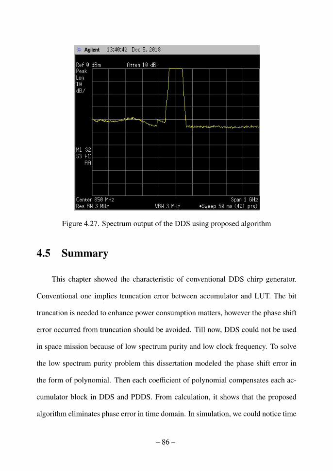
Figure 4.27. Spectrum output of the DDS using proposed algorithm
4.5 Summary
This chapter showed the characteristic of conventional DDS chirp generator.
Conventional one implies truncation error between accumulator and LUT. The bit
truncation is needed to enhance power consumption matters, however the phase shift
error occurred from truncation should be avoided. Till now, DDS could not be used
in space mission because of low spectrum purity and low clock frequency. To solve
the low spectrum purity problem this dissertation modeled the phase shift error in
the form of polynomial. Then each coefficient of polynomial compensates each ac-
cumulator block in DDS and PDDS. From calculation, it shows that the proposed
algorithm eliminates phase error in time domain. In simulation, we could notice time
– 86 –
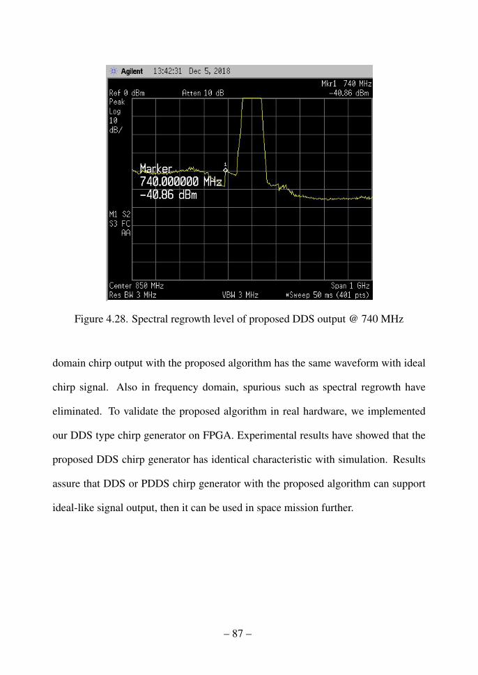
Figure 4.28. Spectral regrowth level of proposed DDS output @ 740 MHz
domain chirp output with the proposed algorithm has the same waveform with ideal
chirp signal. Also in frequency domain, spurious such as spectral regrowth have
eliminated. To validate the proposed algorithm in real hardware, we implemented
our DDS type chirp generator on FPGA. Experimental results have showed that the
proposed DDS chirp generator has identical characteristic with simulation. Results
assure that DDS or PDDS chirp generator with the proposed algorithm can support
ideal-like signal output, then it can be used in space mission further.
– 87 –
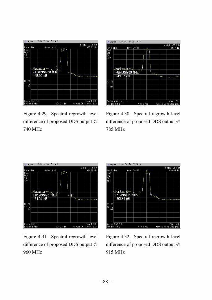
Figure 4.29. Spectral regrowth level
difference of proposed DDS output @
740 MHz
Figure 4.30. Spectral regrowth level
difference of proposed DDS output @
785 MHz
Figure 4.31. Spectral regrowth level
difference of proposed DDS output @
960 MHz
Figure 4.32. Spectral regrowth level
difference of proposed DDS output @
915 MHz
– 88 –
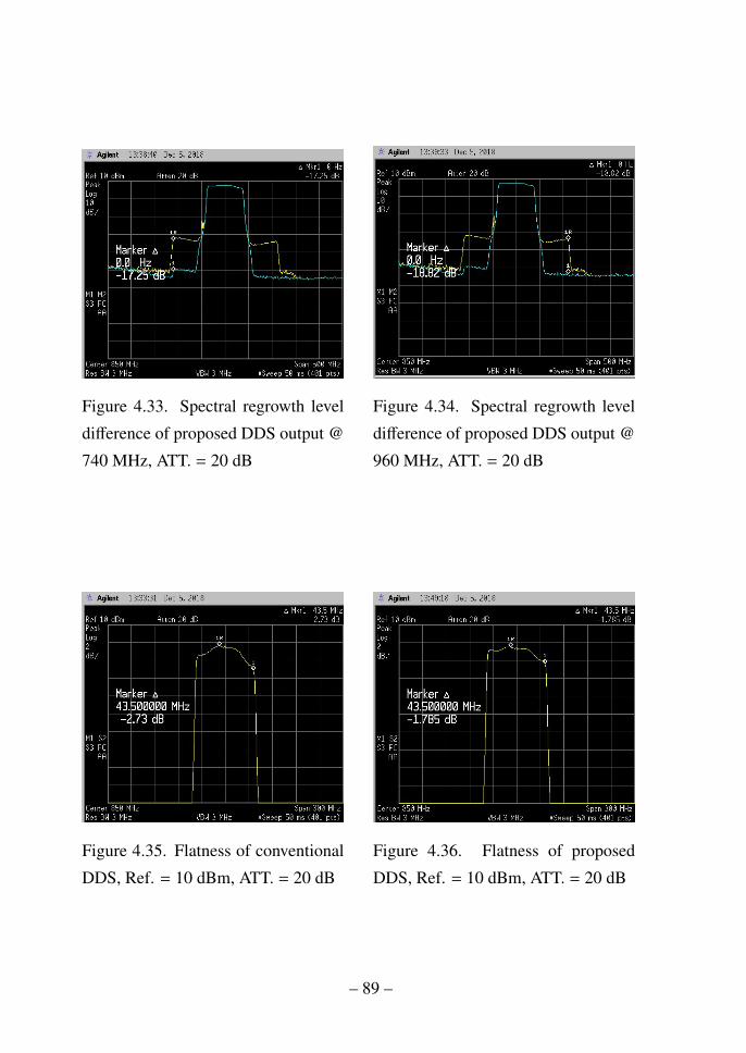
Figure 4.33. Spectral regrowth level
difference of proposed DDS output @
740 MHz, ATT. = 20 dB
Figure 4.34. Spectral regrowth level
difference of proposed DDS output @
960 MHz, ATT. = 20 dB
Figure 4.35. Flatness of conventional
DDS, Ref. = 10 dBm, ATT. = 20 dB
Figure 4.36. Flatness of proposed
DDS, Ref. = 10 dBm, ATT. = 20 dB
– 89 –

Figure 4.37. Comparison of flatness between conventional DDS and conventional
DDS
– 90 –
Chapter 5. Conclusion
SAR is required to support high-resolution images of target in remote area. To
achieve high-resolution images SAR adopts two techniques called synthetic aperture
and linear frequency modulation. Synthetic aperture is a technique which RAR syn-
thesizes its aperture in post processing stage to widen the virtual antenna length in
azimuth direction. On the other hand, linearly frequency modulated signal called
chirp is used to enhance the resolution in range direction. Due to its versatility, the
demand on SAR image is getting enormously enlarging. Therefore, research on de-
velopment of SAR system with wide bandwidth is being important.
Conventionally, memory-map based chirp generator is frequently used in SAR
systems. It supports ideal-like signal characteristics in the respect of frequency lin-
earity, spectrum purity, spurious, and etc. However, when it comes to generate wide
bandwidth and long pulse width signal memory-map based chirp generator requires
large amount of memory space. It takes long time to update chirp information in
the case the memory unit get damaged. Especially in space mission, memory unit
is vulnerable to cosmic so that it can lost its bit information easily. Therefore this
dissertation proposes DDS type chirp generator. DDS has minimum memory for one
cycle of sinusoid information, therefore it has strong point over memory damage.
Because DDS truncates its information during signal generation process, however, it
has phase shift in time domain which leads to spurious in frequency domain. This
– 91 –

research starts from that DDS also can be used in various SAR payloads if the phase
error could be eliminated. The proposed phase error compensation algorithm consists
of two parts. First, it models phase error from LUT output using 2nd order polyno-
mial. Next, the proposed algorithm compensates each accumulator error using error
coefficients. To validate the proposed algorithm, we implemented DDS and PDDS
chirp generator on FPGA. From numerical expression and simulation we could re-
alize that phase error in time domain is eliminated ideally. Also, when the results
are examined using IRF and spectrum, PSLR and ISLR are improved and spurious
is eliminated. Even in experiment, we could notice that experimental result follows
the simulation.
The contributions of this thesis is as follows:
• A general model for satellite on-board SAR system has been presented.
• The phase shifting phenomenon in PDDS chirp signal generator has been re-
vealed.
• A model for phase error compensation method has been proposed and perfor-
mance analysis of PDDS chirp signal generator in baseband and IF stage has
been presented in the respect of time and frequency domain.
• A RF stage simulation model has been presented to evaluate the effect of RF
impairments.
• An IRF characteristic of proposed PDDS signal has been increased compared
to conventional PDDS chirp signal generator; PSLR = -0.2645 dB enhanced,
– 92 –

ISLR = -0.1788 dB enhanced.
Since the proposed method considers practical DDS and PDDS chirp signal
generator, and the results show considerable performance enhancements, it is ex-
pected that proposed PDDS chirp signal generator using error compensation method
can be applied to conventional DDS and replace the memory-map based chirp signal
generator frequently used in satellite on-board SAR systems.
– 93 –

References
[1] J. C. Curlander and R. N. McDonough, Synthetic aperture radar. John Wiley
& Sons, 1991.
[2] I. G. Cumming and F. H.-c. Wong, Digital processing of synthetic aperture
radar data: algorithms and implementation. Artech House, 2005.
[3] K. Tomiyasu, “Tutorial review of synthetic-aperture radar (sar) with applica-
tions to imaging of the ocean surface,” Proceedings of the IEEE, vol. 66, no. 5,
pp. 563–583, 1978.
[4] Y. Sharay and U. Naftaly, “Tecsar: design considerations and programme sta-
tus,” IEE Proceedings-Radar, Sonar and Navigation, vol. 153, no. 2, pp. 117–
121, 2006.
[5] A. Torre and P. Capece, “Cosmo-skymed: The advanced sar instrument,” in
Recent Advances in Space Technologies (RAST), 2011 5th International Con-
ference on. IEEE, 2011, pp. 865–868.
[6] H. Yang and J.-H. Kim, “Implementation of dds chirp signal generator on fpga,”
ICTC 2014, Oct. 2014.
– 94 –
[7] S.-R. Lee, “Overview of kompsat-5 program, mission, and system,” in Geo-
science and Remote Sensing Symposium (IGARSS), 2010 IEEE International.
IEEE, 2010, pp. 797–800.
[8] S.-B. Ryu, J.-P. Kim, J.-H. Yang, Y.-J. Won, and S.-K. Lee, “Study of rf im-
pairments in wideband chirp signal generator,” The Journal of Korean Institute
of Electromagnetic Engineering and Science, vol. 24, no. 12, pp. 1205–1214,
2013.
[9] I. Cumming and J. Bennett, “Digital processing of seasat sar data,” in Acoustics,
Speech, and Signal Processing, IEEE International Conference on ICASSP’79.,
vol. 4. IEEE, 1979, pp. 710–718.
[10] J. Fransson, F. Walter, and H. Olsson, “Identification of clear felled areas using
spot p and almaz-1 sar data,” International Journal of Remote Sensing, vol. 20,
no. 18, pp. 3583–3593, 1999.
[11] M. C. Dobson, L. E. Pierce, and F. T. Ulaby, “Knowledge-based land-cover
classification using ers-1/jers-1 sar composites,” IEEE Transactions on Geo-
science and Remote Sensing, vol. 34, no. 1, pp. 83–99, 1996.
[12] A. Rosenqvist, M. Shimada, B. Chapman, K. McDonald, G. De Grandi, H. Jon-
sson, C. Williams, Y. Rauste, M. Nilsson, D. Sango et al., “An overview of the
jers-1 sar global boreal forest mapping (gbfm) project,” in Geoscience and Re-
mote Sensing Symposium, 2004. IGARSS’04. Proceedings. 2004 IEEE Interna-
tional, vol. 2. IEEE, 2004, pp. 1033–1036.
– 95 –

[13] R. K. Raney, A. P. Luscombe, E. Langham, and S. Ahmed, “Radarsat (sar imag-
ing),” Proceedings of the IEEE, vol. 79, no. 6, pp. 839–849, 1991.
[14] A. Rosenqvist, M. Shimada, N. Ito, and M. Watanabe, “Alos palsar: A
pathfinder mission for global-scale monitoring of the environment,” IEEE
Transactions on Geoscience and Remote Sensing, vol. 45, no. 11, pp. 3307–
3316, 2007.
[15] R. Werninghaus and S. Buckreuss, “The terrasar-x mission and system design,”
IEEE Transactions on Geoscience and Remote Sensing, vol. 48, no. 2, pp. 606–
614, 2010.
[16] J. Yoon, J. Keum, J. Shin, J. Kim, S. Lee, A. Bauleo, C. Farina, C. Germani,
M. Mappini, and R. Venturini, “Kompsat-5 sar design and performance,” in
Synthetic Aperture Radar (APSAR), 2011 3rd International Asia-Pacific Con-
ference on. IEEE, 2011, pp. 1–4.
[17] Y. Zhen and Y. Ruliang, “Feasibility study of using small satellite synthetic
aperture radar for global 3d imaging,” in Geoscience and Remote Sensing Sym-
posium, 2002. IGARSS ’02. 2002 IEEE International, vol. 6, 2002, pp. 3162–
3164 vol.6.
[18] J. Sumantyo and K. Ito, “Circularly polarised equilateral triangular patch ar-
ray antenna for mobile satellite communications,” Microwaves, Antennas and
Propagation, IEE Proceedings, vol. 153, no. 6, pp. 544–550, Dec. 2006.
– 96 –
[19] J. Sumantyo and K. Voon-Chet, “Development of synthetic aperture radar on-
board unmanned aerial vehicle,” in 2013 Asia-Pacific Conference on Synthetic
Aperture Radar (APSAR), Sep. 2013, pp. 37–40.
[20] M. Y. Chua and V. C. Koo, “Fpga-based chirp generator for high resolution uav
sar,” Progress In Electromagnetics Research, vol. 99, pp. 71–88, 2009.
[21] A. Samarah and O. Loffeld, “An improved digital chirp generator using opti-
mized piecewise- polynomial approximations,” in 2010 8th European Confer-
ence on Synthetic Aperture Radar (EUSAR), Jun. 2010, pp. 1–4.
[22] S. Buckreuss, W. Balzer, P. Muhlbauer, R. Werninghaus, and W. Pitz, “The
terrasar-x satellite project,” in Geoscience and remote sensing symposium,
2003. IGARSS’03. Proceedings. 2003 IEEE International, vol. 5. IEEE, 2003,
pp. 3096–3098.
[23] K. Suto, J. Sumantyo, V. Koo, M. Chua, and W. Cheaw, “Development of sar
base-band signal processor using fpga and onboard pc,” in Geoscience and Re-
mote Sensing Symposium (IGARSS), 2014 IEEE International. IEEE, 2014,
pp. 672–675.
[24] F. Argenti, A. Lapini, T. Bianchi, and L. Alparone, “A tutorial on speckle reduc-
tion in synthetic aperture radar images,” IEEE Geoscience and remote sensing
magazine, vol. 1, no. 3, pp. 6–35, 2013.
[25] V. Wissan, I. Firmansyah, P. Rizki Akbar, J. T. Sri Sumantyo, H. Kuze et al.,
“Development of circularly polarized array antenna for synthetic aperture radar
– 97 –
sensor installed on uav,” Progress In Electromagnetics Research, vol. 19, pp.
119–133, 2011.
[26] M. Virelli, A. Coletta, and M. L. Battagliere, “Asi cosmo-skymed: Mission
overview and data exploitation,” IEEE Geoscience and Remote Sensing Maga-
zine, vol. 2, no. 2, pp. 64–66, 2014.
[27] A. Samarah, A Novel Approach for Generating Digital Chirp Signals Using
FPGA Technology for Synthetic Aperture Radar Applications, 2012.
[28] J. Tierney, C. M. Rader, and B. Gold, “A digital frequency synthesizer,” Audio
and Electroacoustics, IEEE Transactions on, vol. 19, no. 1, pp. 48–57, 1971.
[29] M. Xing, X. Jiang, R. Wu, F. Zhou, and Z. Bao, “Motion compensation for uav
sar based on raw radar data,” IEEE Transactions on Geoscience and Remote
Sensing, vol. 47, no. 8, pp. 2870–2883, 2009.
[30] P. A. Rosen, S. Hensley, K. Wheeler, G. Sadowy, T. Miller, S. Shaffer,
R. Muellerschoen, C. Jones, H. Zebker, and S. Madsen, “Uavsar: A new nasa
airborne sar system for science and technology research,” in Radar, 2006 IEEE
Conference on. IEEE, 2006, pp. 8–pp.
[31] E. Chapin, A. Chau, J. Chen, B. Heavey, S. Hensley, Y. Lou, R. Machuzak,
and M. Moghaddam, “Airmoss: An airborne p-band sar to measure root-zone
soil moisture,” in Radar Conference (RADAR), 2012 IEEE. IEEE, 2012, pp.
0693–0698.
– 98 –

[32] M. Edwards, D. Madsen, C. Stringham, A. Margulis, B. Wicks, and D. G. Long,
“microasar: A small, robust lfm-cw sar for operation on uavs and small air-
craft,” in Geoscience and Remote Sensing Symposium, 2008. IGARSS 2008.
IEEE International, vol. 5. IEEE, 2008, pp. V–514.
[33] T. Steeghs, D. van Halsema, and P. Hoogeboom, MiniSAR: a miniature,
lightweight, low cost, scalable SAR system. Tokyo: National Space Devel-
opment Agency of Japan (NASDA), 2001.
[34] W. Jian, L. Jin-mei, Y. Yuan, and F. Jun, “Research on application of unmanned
aerial vehicles borne sar,” in Synthetic Aperture Radar, 2009. APSAR 2009. 2nd
Asian-Pacific Conference on. IEEE, 2009, pp. 60–63.
[35] C. Bhattacharya, A. Roy, S. Navneet, A. Heddallikar, and R. Pinto, “Microsar:
calibration of x-band high resolution fmcw synthetic aperture radar (sar),” in
Microwave and RF Conference (IMaRC), 2014 IEEE International. IEEE,
2014, pp. 377–380.
[36] H. Saito and J. S. Sumantyo, “Synthetic aperture radar for uavs and small satel-
lites,” The IEICE Transactions of Communications, vol. 97, pp. 992–998.
[37] Y. Kankaku, “The overview of the l-band sar onboard alos-2, progress,” in Elec-
tromagnetics Research Symposium Proceedings, 2009, 2009.
[38] N. Salerno, L. Simone, S. Cocchi, V. Piloni, M. Maffei, and O. Cocciolillo,
“Wideband arbitrary waveform generator for enhanced spaceborne sar,” in
Radar Conference, 2008. EuRAD 2008. European. IEEE, 2008, pp. 416–419.
– 99 –
[39] M. Shimada, “Radiometric and geometric calibration of jers-1 sar,” Advances
in Space Research, vol. 17, no. 1, pp. 79–88, 1996.
[40] H. Yang, G. F. Panggabean, A. Hendra, B. Purbantoro, C. E. Santosa, K. Naka-
mura, Y. Izumi, J. T. S. Sumantyo, and K.-R. Kim, “Conceptual design of high-
resolution x-band unmanned aerial vehicle (uav) on-board synthetic aperture
radar,” Progress and Communication in Sciences, vol. 2, no. 1, pp. 14–22, 2015.
[41] J. T. S. Sumantyo, K. V. Chet, and R. H. Triharjanto, “Development of circularly
polarized synthetic aperture radar onboard unmanned aerial vehicle,” in Geo-
science and Remote Sensing Symposium (IGARSS), 2013 IEEE International.
IEEE, 2013, pp. 2301–2304.
[42] V. C. Koo, Y. K. Chan, G. Vetharatnam, M. Y. Chua, C. H. Lim, C.-S. Lim,
C. Thum, T. S. Lim, Z. bin Ahmad, K. A. Mahmood et al., “A new unmanned
aerial vehicle synthetic aperture radar for environmental monitoring,” Progress
In Electromagnetics Research, vol. 122, pp. 245–268, 2012.
[43] L. Cordesses, “Direct digital synthesis: A tool for periodic wave generation
(part 1),” IEEE Signal processing magazine, vol. 21, no. 4, pp. 50–54, 2004.
[44] V. F. Kroupa, Direct digital frequency synthesizers. IEEE, 1999.
[45] H. Yang, J. T. S. Sumantyo, J.-H. An, H.-W. Jung, and J.-H. Kim, “Phase error
compensation method using polynomial model for a direct digital synthesizer
based chirp signal generator,” in Geoscience and Remote Sensing Symposium
(IGARSS), 2015 IEEE International. IEEE, 2015, pp. 786–789.
– 100 –
[46] J. An, H. Jung, H. Yang, S.-B. Ryu, H.-C. Lee, S.-G. Lee, S.-S. Yong, and
J.-H. Kim, “Development of chirp signal generator for micro satellite on-
board synthetic aperture radar,” in Geoscience and Remote Sensing Symposium
(IGARSS), 2015 IEEE International. IEEE, 2015, pp. 3663–3666.
[47] J. Zhang, F. Mu, Q. Shi, and X. He, “Design and implementation of multi-
channel wideband and rf signal generator,” in Computational Science and En-
gineering (CSE), 2014 IEEE 17th International Conference on. IEEE, 2014,
pp. 1566–1569.
[48] J. Liao, X. Ye, X. Hu, and D. Sun, “Research and implementation on multi-dds
technology in high performance digital up-conversion,” in Industrial Electron-
ics and Applications (ICIEA), 2013 8th IEEE Conference on. IEEE, 2013, pp.
178–183.
[49] M. Pichler, A. Stelzer, P. Gulden, C. Seisenberger, and M. Vossiek, “Phase-
error measurement and compensation in pll frequency synthesizers for fmcw
sensors—i: Context and application,” IEEE Transactions on Circuits and Sys-
tems I: Regular Papers, vol. 54, no. 5, pp. 1006–1017, 2007.
[50] V. F. Kroupa, V. Cizek, J. Stursa, and H. Svandova, “Spurious signals in direct
digital frequency synthesizers due to the phase truncation,” IEEE transactions
on ultrasonics, ferroelectrics, and frequency control, vol. 47, no. 5, pp. 1166–
1172, 2000.
– 101 –

[51] J.-P. K. Sang-Burm Ryu, “Study of RF impairments in wideband chirp signal
generator,” The Journal of Korean Institute of Electromagnetic Engineering and
Science, vol. 24, no. 12, 2013.
– 102 –