Design of Robust, Energy-Efficient Full Adders for Deep ...
13
IEEE TRANSACTIONS ON VERY LARGE SCALE INTEGRATION (VLSI) SYSTEMS, VOL. 14, NO. 12, DECEMBER 2006 1309 Design of Robust, Energy-Efficient Full Adders for Deep-Submicrometer Design Using Hybrid-CMOS Logic Style Sumeer Goel, Student Member, IEEE, Ashok Kumar, Senior Member, IEEE, and Magdy A. Bayoumi, Fellow, IEEE Abstract—We present a new design for a 1-b full adder featuring hybrid-CMOS design style. The quest to achieve a good-drivability, noise-robustness, and low-energy operations for deep submicrom- eter guided our research to explore hybrid-CMOS style design. Hybrid-CMOS design style utilizes various CMOS logic style cir- cuits to build new full adders with desired performance. This pro- vides the designer a higher degree of design freedom to target a wide range of applications, thus significantly reducing design ef- forts. We also classify hybrid-CMOS full adders into three broad categories based upon their structure. Using this categorization, many full-adder designs can be conceived. We will present a new full-adder design belonging to one of the proposed categories. The new full adder is based on a novel XOR–XNOR circuit that generates XOR and XNOR full-swing outputs simultaneously. This circuit outperforms its counterparts showing 5%–37% improve- ment in the power-delay product (PDP). A novel hybrid-CMOS output stage that exploits the simultaneous XOR–XNOR signals is also proposed. This output stage provides good driving capability enabling cascading of adders without the need of buffer insertion between cascaded stages. There is approximately a 40% reduction in PDP when compared to its best counterpart. During our experimentations, we found out that many of the pre- viously reported adders suffered from the problems of low swing and high noise when operated at low supply voltages. The pro- posed full adder is energy efficient and outperforms several stan- dard full adders without trading off driving capability and relia- bility. The new full-adder circuit successfully operates at low volt- ages with excellent signal integrity and driving capability. To eval- uate the performance of the new full adder in a real circuit, we em- bedded it in a 4- and 8-b, 4-operand carry-save array adder with final carry-propagate adder. The new adder displayed better per- formance as compared to the standard full adders. Index Terms—Adders, deep-submicrometer design, hybrid- CMOS design style, low-power, noise. I. INTRODUCTION T HE DEMAND and popularity of portable electronics is driving designers to strive for smaller silicon area, higher speeds, longer battery life, and more reliability. Power is one of the premium resources a designer tries to save when designing a system. Full adders are fundamental units in various circuits, especially in circuits used for performing arithmetic operations Manuscript received May 12, 2005; revised February 10, 2006 and June 1, 2006. This work was supported in part by the U.S. Department of Energy and by the Governor’s Information Technology Initiative. The authors are with the Center for Advanced Computer Studies, University of Louisiana at Lafayette, Lafayette, LA 70504 USA (e-mail: sxg4999@cacs. louisiana.ed; [email protected]; [email protected]). Digital Object Identifier 10.1109/TVLSI.2006.887807 Fig. 1. Power breakdown in high-performance microprocessors [2]. such as compressors, comparators, parity checkers, and so on [1]. Full adders are often in the critical paths of complex arith- metic circuits for multiplication and division. These in turn form the core of any system and thereby influence the overall per- formance of the entire system. Enhancing the performance of the full adder can significantly affect the system performance. Fig. 1 shows the power consumption breakdown in a modern day high-performance microprocessor [2]. The datapath con- sumes roughly 30% of the total power of the system. Adders are an extensively used component in datapaths and, therefore, careful design and analysis is required for these units to obtain optimum performance. At the circuit level, an optimized design is desired to avoid any degradation in the output voltage, consume less power, have less delay in critical path, and be reliable even at low supply voltage as we scale towards deep submicrometer. Good driving capability under different load conditions and balanced output to avoid glitches is also an important virtue. Since the full-adder cells are duplicated in large numbers, layout regularity, and in- terconnect complexity are also important. Several logic styles have been used in the past to design full- adder cells. Each design style has its own merits and demerits. Classical designs of full adders normally use only one logic style for the whole full-adder design. One example of such de- sign is the standard static CMOS full adder [3]. This full adder is based on regular CMOS structure with conventional pull-up and pull-down transistors providing full-swing output and good driving capabilities. The main drawback of static CMOS circuits is the existence of the pMOS block, because of its low mobility compared to the nMOS devices. Therefore, the pMOS devices need to be sized up to attain the desired performance. The input capacitance of a static CMOS gate is large because each input is connected to the gate of at least a pMOS and a nMOS device. 1063-8210/$20.00 © 2006 IEEE Authorized licensed use limited to: Shahid Beheshti University. Downloaded on November 5, 2009 at 02:38 from IEEE Xplore. Restrictions apply.
Transcript of Design of Robust, Energy-Efficient Full Adders for Deep ...

IEEE TRANSACTIONS ON VERY LARGE SCALE INTEGRATION (VLSI) SYSTEMS, VOL. 14, NO. 12, DECEMBER 2006 1309
Design of Robust, Energy-Efficient Full Addersfor Deep-Submicrometer Design Using
Hybrid-CMOS Logic StyleSumeer Goel, Student Member, IEEE, Ashok Kumar, Senior Member, IEEE, and Magdy A. Bayoumi, Fellow, IEEE
Abstract—We present a new design for a 1-b full adder featuringhybrid-CMOS design style. The quest to achieve a good-drivability,noise-robustness, and low-energy operations for deep submicrom-eter guided our research to explore hybrid-CMOS style design.Hybrid-CMOS design style utilizes various CMOS logic style cir-cuits to build new full adders with desired performance. This pro-vides the designer a higher degree of design freedom to target awide range of applications, thus significantly reducing design ef-forts. We also classify hybrid-CMOS full adders into three broadcategories based upon their structure. Using this categorization,many full-adder designs can be conceived. We will present a newfull-adder design belonging to one of the proposed categories.
The new full adder is based on a novel XOR–XNOR circuit thatgenerates XOR and XNOR full-swing outputs simultaneously. Thiscircuit outperforms its counterparts showing 5%–37% improve-ment in the power-delay product (PDP). A novel hybrid-CMOSoutput stage that exploits the simultaneous XOR–XNOR signals isalso proposed. This output stage provides good driving capabilityenabling cascading of adders without the need of buffer insertionbetween cascaded stages. There is approximately a 40% reductionin PDP when compared to its best counterpart.
During our experimentations, we found out that many of the pre-viously reported adders suffered from the problems of low swingand high noise when operated at low supply voltages. The pro-posed full adder is energy efficient and outperforms several stan-dard full adders without trading off driving capability and relia-bility. The new full-adder circuit successfully operates at low volt-ages with excellent signal integrity and driving capability. To eval-uate the performance of the new full adder in a real circuit, we em-bedded it in a 4- and 8-b, 4-operand carry-save array adder withfinal carry-propagate adder. The new adder displayed better per-formance as compared to the standard full adders.
Index Terms—Adders, deep-submicrometer design, hybrid-CMOS design style, low-power, noise.
I. INTRODUCTION
THE DEMAND and popularity of portable electronics isdriving designers to strive for smaller silicon area, higher
speeds, longer battery life, and more reliability. Power is one ofthe premium resources a designer tries to save when designinga system. Full adders are fundamental units in various circuits,especially in circuits used for performing arithmetic operations
Manuscript received May 12, 2005; revised February 10, 2006 and June 1,2006. This work was supported in part by the U.S. Department of Energy andby the Governor’s Information Technology Initiative.
The authors are with the Center for Advanced Computer Studies, Universityof Louisiana at Lafayette, Lafayette, LA 70504 USA (e-mail: [email protected]; [email protected]; [email protected]).
Digital Object Identifier 10.1109/TVLSI.2006.887807
Fig. 1. Power breakdown in high-performance microprocessors [2].
such as compressors, comparators, parity checkers, and so on[1]. Full adders are often in the critical paths of complex arith-metic circuits for multiplication and division. These in turn formthe core of any system and thereby influence the overall per-formance of the entire system. Enhancing the performance ofthe full adder can significantly affect the system performance.Fig. 1 shows the power consumption breakdown in a modernday high-performance microprocessor [2]. The datapath con-sumes roughly 30% of the total power of the system. Addersare an extensively used component in datapaths and, therefore,careful design and analysis is required for these units to obtainoptimum performance.
At the circuit level, an optimized design is desired to avoidany degradation in the output voltage, consume less power, haveless delay in critical path, and be reliable even at low supplyvoltage as we scale towards deep submicrometer. Good drivingcapability under different load conditions and balanced outputto avoid glitches is also an important virtue. Since the full-addercells are duplicated in large numbers, layout regularity, and in-terconnect complexity are also important.
Several logic styles have been used in the past to design full-adder cells. Each design style has its own merits and demerits.Classical designs of full adders normally use only one logicstyle for the whole full-adder design. One example of such de-sign is the standard static CMOS full adder [3]. This full adderis based on regular CMOS structure with conventional pull-upand pull-down transistors providing full-swing output and gooddriving capabilities. The main drawback of static CMOS circuitsis the existence of the pMOS block, because of its low mobilitycompared to the nMOS devices. Therefore, the pMOS devicesneed to be sized up to attain the desired performance. The inputcapacitance of a static CMOS gate is large because each inputis connected to the gate of at least a pMOS and a nMOS device.
1063-8210/$20.00 © 2006 IEEE
Authorized licensed use limited to: Shahid Beheshti University. Downloaded on November 5, 2009 at 02:38 from IEEE Xplore. Restrictions apply.
1310 IEEE TRANSACTIONS ON VERY LARGE SCALE INTEGRATION (VLSI) SYSTEMS, VOL. 14, NO. 12, DECEMBER 2006
This is another reason for speed degradation of static CMOSgates.
Another conventional adder is the complementary pass-tran-sistor logic (CPL) [3]. It provides high-speed, full-swing opera-tion and good driving capability due to the output static invertersand the fast differential stage of cross-coupled pMOS transis-tors. But due to the presence of a lot of internal nodes and staticinverters, there is large power dissipation. The layout of a CPLcell is also not as straightforward as a static CMOS cell due toits irregular transistor arrangement.
The dynamic CMOS logic style provides a high speed of op-eration because the logic is constructed with only high mobilitynMOS transistors. Also, due to the absence of the pMOS transis-tors, the input capacitance is also low, thus enhancing the speedof operation. However, it has several inherent problems such ascharge sharing and high clock load. It has higher switching ac-tivity and lower noise immunity. It consumes a large portion ofthe power in driving the clock lines. Moreover, dynamic logicstyle is more susceptible to leakage. Due to these reasons, we donot include dynamic logic style in our discussions in this paper.
Some other full-adder designs include transmission-functionfull adder (TFA) [4] and transmission-gate full adder (TGA) [5].These designs are based on transmission-function theory andtransmission gates, respectively. These adders are inherentlylow power consuming. These logic styles are good for designingXOR or XNOR gates. The main disadvantage of these logic stylesis that they lack driving capability. This is attributed to the factthat the inputs are coupled to the outputs. When TGA or TFAare cascaded, their performance degrades significantly.
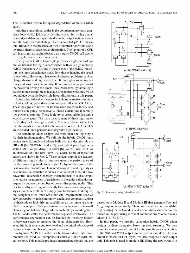
The remaining adder designs use more than one logic stylefor their implementation. We call this the hybrid-CMOS logicdesign style. Examples of adders built with this design style areDB cell [6], NEW14-T adder [7], and hybrid pass logic withstatic CMOS output drive full adder [8] (we will use HPSC asan abbreviation) and new-HPSC [9] adder. Some of these fulladders are shown in Fig. 2. These designs exploit the featuresof different logic styles to improve upon the performance ofthe designs using single logic style. All hybrid designs use thebest available modules implemented using different logic stylesor enhance the available modules in an attempt to build a lowpower full-adder cell. Generally, the main focus in such attemptsis to reduce the numbers of transistors in the adder cell and, con-sequently, reduce the number of power dissipating nodes. Thisis achieved by utilizing intrinsically low power consuming logicstyles like TFA or TGA or simply pass transistors. In doing so,the designers often trade off other vital requirements such asdriving capability, noise immunity, and layout complexity. Mostof these adders lack driving capabilities as the inputs are cou-pled to the outputs. Their performance as a single unit or in smallchains is good but when large adders are built by cascading these1-b full-adder cells, the performance degrades drastically. Theperformance degradation can be handled by inserting buffersin between stages to enhance the delay characteristics. How-ever, this leads to an extra overhead and the initial advantage ofhaving a lesser number of transistors is lost.
A hybrid-CMOS full adder can be broken down into threemodules [6]. Module I comprises of either a XOR or XNOR cir-cuit or both. This module produces intermediate signals that are
Fig. 2. Standard existing full-adder cells.
passed onto Module II and Module III that generate Sum andoutputs, respectively. There are several circuits available
in [1] and [6] for each module and several studies have been con-ducted in the past using different combinations to obtain manyadders [1], [6], [10].
In this paper, we broadly categorize hybrid-CMOS adderdesigns in three categories based on their structure. We thenpresent a new improved circuit for the simultaneous generationof the XOR and XNOR outputs to be used in module I. The newcircuit is based on CPL style. We also propose a new outputunit. This unit is used in module III. Using the new circuits in
Authorized licensed use limited to: Shahid Beheshti University. Downloaded on November 5, 2009 at 02:38 from IEEE Xplore. Restrictions apply.
GOEL et al.: DESIGN OF ROBUST, ENERGY-EFFICIENT FULL ADDERS 1311
Fig. 3. General form of XOR–XOR-based full adder.
module I and III, we build a new hybrid-CMOS full-adder cell.The new adder is optimized for low PDP and is compared withthe classical static-CMOS, CPL, TFA, TGA, NEW14T, HPSC,and NEW-HPSC full-adder cells. The proposed full-adderdesign exhibits low PDP, full-swing operation, and excellentdriving capabilities without trading off area and reliability.To evaluate the performance of the new full adder in a realcircuit, we embedded it in a 4- and 8-b, 4-operand carry-savearray adder with final carry-propagate adder. The new adderdisplayed better performance as compared to the standard fulladders and can be cascaded without the need of buffer insertion.
II. FULL-ADDER CATEGORIZATION
We categorize hybrid-CMOS full-adder cells [11] in, broadly,three categories depending upon their structure and logical ex-pression of the Sum output. The Sum and Carry ( ) outputsof a 1-b full adder generated from the binary inputs , , and
can be generally expressed as
(1)
(2)
These outputs can be expressed in many different logic ex-pressions and, thereby, determine the structure of the circuit.Based upon these different logic expressions, many full-addercells can be conceived. Moreover, the availability of differentmodules, as discussed earlier, provides the designer with morechoices for a 1-b adder implementation. We classify the differentpossible structures for full adders into three broad categories.These are as follows.
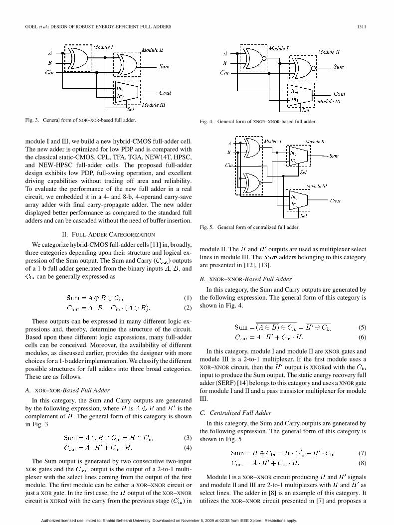
A. XOR–XOR-Based Full Adder
In this category, the Sum and Carry outputs are generatedby the following expression, where is and is thecomplement of . The general form of this category is shownin Fig. 3
(3)
(4)
The Sum output is generated by two consecutive two-inputXOR gates and the output is the output of a 2-to-1 multi-plexer with the select lines coming from the output of the firstmodule. The first module can be either a XOR–XNOR circuit orjust a XOR gate. In the first case, the output of the XOR–XNOR
circuit is XORed with the carry from the previous stage ( ) in
Fig. 4. General form of XNOR–XNOR-based full adder.
Fig. 5. General form of centralized full adder.
module II. The and outputs are used as multiplexer selectlines in module III. The adders belonging to this categoryare presented in [12], [13].
B. XNOR–XNOR-Based Full Adder
In this category, the Sum and Carry outputs are generated bythe following expression. The general form of this category isshown in Fig. 4.
(5)
(6)
In this category, module I and module II are XNOR gates andmodule III is a 2-to-1 multiplexer. If the first module uses aXOR–XNOR circuit, then the output is XNORed with theinput to produce the Sum output. The static energy recovery fulladder (SERF) [14] belongs to this category and uses a XNOR gatefor module I and II and a pass transistor multiplexer for moduleIII.
C. Centralized Full Adder
In this category, the Sum and Carry outputs are generated bythe following expression. The general form of this category isshown in Fig. 5
(7)
(8)
Module I is a XOR–XNOR circuit producing and signalsand module II and III are 2-to-1 multiplexers with and asselect lines. The adder in [8] is an example of this category. Itutilizes the XOR–XNOR circuit presented in [7] and proposes a
Authorized licensed use limited to: Shahid Beheshti University. Downloaded on November 5, 2009 at 02:38 from IEEE Xplore. Restrictions apply.
1312 IEEE TRANSACTIONS ON VERY LARGE SCALE INTEGRATION (VLSI) SYSTEMS, VOL. 14, NO. 12, DECEMBER 2006
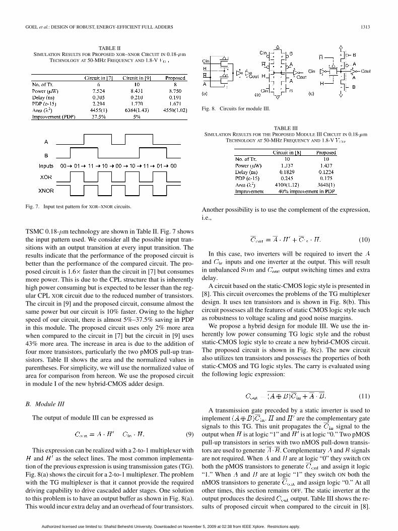
Fig. 6. (a) Circuit in [7]. (b) Circuit in [9]. (c) Proposed circuit.
new circuit for output module III. The simultaneous generationof and signal is critical in these types of adders as theydrive the select lines of the multiplexers in the output stage. Inanother case (i.e., nonsimultaneous and ), there may beglitches and unnecessary power dissipation may occur. The finaloutputs cannot be generated until these intermediate signals areavailable from module I.
III. PROPOSED CIRCUITS FOR MODULE I AND III
Hybrid-CMOS full adders can be divided into three modules[6]. Module I consists of either an XOR or XNOR circuit. ModuleII and module III generate and . We present two newcircuits, one for each module I and module III.
A. Module I
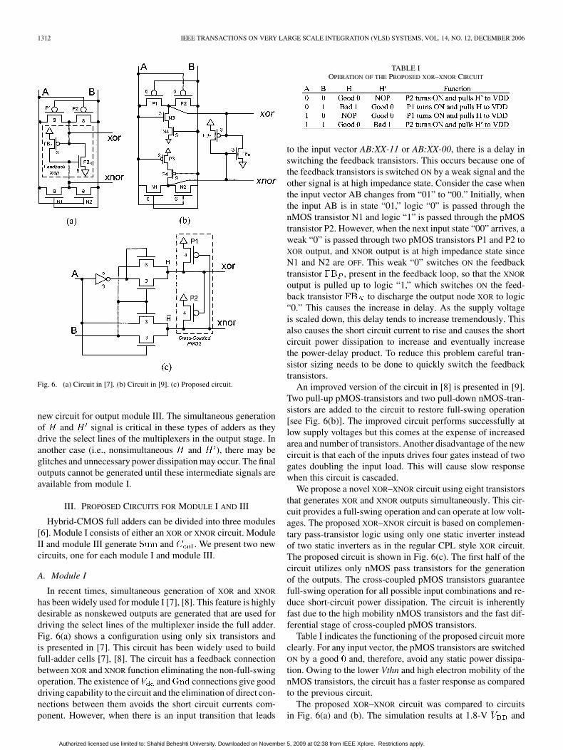
In recent times, simultaneous generation of XOR and XNOR
has been widely used for module I [7], [8]. This feature is highlydesirable as nonskewed outputs are generated that are used fordriving the select lines of the multiplexer inside the full adder.Fig. 6(a) shows a configuration using only six transistors andis presented in [7]. This circuit has been widely used to buildfull-adder cells [7], [8]. The circuit has a feedback connectionbetween XOR and XNOR function eliminating the non-full-swingoperation. The existence of and connections give gooddriving capability to the circuit and the elimination of direct con-nections between them avoids the short circuit currents com-ponent. However, when there is an input transition that leads
TABLE IOPERATION OF THE PROPOSED XOR–XNOR CIRCUIT
to the input vector AB:XX-11 or AB:XX-00, there is a delay inswitching the feedback transistors. This occurs because one ofthe feedback transistors is switched ON by a weak signal and theother signal is at high impedance state. Consider the case whenthe input vector AB changes from “01” to “00.” Initially, whenthe input AB is in state “01,” logic “0” is passed through thenMOS transistor N1 and logic “1” is passed through the pMOStransistor P2. However, when the next input state “00” arrives, aweak “0” is passed through two pMOS transistors P1 and P2 toXOR output, and XNOR output is at high impedance state sinceN1 and N2 are OFF. This weak “0” switches ON the feedbacktransistor , present in the feedback loop, so that the XNOR
output is pulled up to logic “1,” which switches ON the feed-back transistor to discharge the output node XOR to logic“0.” This causes the increase in delay. As the supply voltageis scaled down, this delay tends to increase tremendously. Thisalso causes the short circuit current to rise and causes the shortcircuit power dissipation to increase and eventually increasethe power-delay product. To reduce this problem careful tran-sistor sizing needs to be done to quickly switch the feedbacktransistors.
An improved version of the circuit in [8] is presented in [9].Two pull-up pMOS-transistors and two pull-down nMOS-tran-sistors are added to the circuit to restore full-swing operation[see Fig. 6(b)]. The improved circuit performs successfully atlow supply voltages but this comes at the expense of increasedarea and number of transistors. Another disadvantage of the newcircuit is that each of the inputs drives four gates instead of twogates doubling the input load. This will cause slow responsewhen this circuit is cascaded.
We propose a novel XOR–XNOR circuit using eight transistorsthat generates XOR and XNOR outputs simultaneously. This cir-cuit provides a full-swing operation and can operate at low volt-ages. The proposed XOR–XNOR circuit is based on complemen-tary pass-transistor logic using only one static inverter insteadof two static inverters as in the regular CPL style XOR circuit.The proposed circuit is shown in Fig. 6(c). The first half of thecircuit utilizes only nMOS pass transistors for the generationof the outputs. The cross-coupled pMOS transistors guaranteefull-swing operation for all possible input combinations and re-duce short-circuit power dissipation. The circuit is inherentlyfast due to the high mobility nMOS transistors and the fast dif-ferential stage of cross-coupled pMOS transistors.
Table I indicates the functioning of the proposed circuit moreclearly. For any input vector, the pMOS transistors are switchedON by a good and, therefore, avoid any static power dissipa-tion. Owing to the lower Vthn and high electron mobility of thenMOS transistors, the circuit has a faster response as comparedto the previous circuit.
The proposed XOR–XNOR circuit was compared to circuitsin Fig. 6(a) and (b). The simulation results at 1.8-V and
Authorized licensed use limited to: Shahid Beheshti University. Downloaded on November 5, 2009 at 02:38 from IEEE Xplore. Restrictions apply.
GOEL et al.: DESIGN OF ROBUST, ENERGY-EFFICIENT FULL ADDERS 1313
TABLE IISIMULATION RESULTS FOR PROPOSED XOR–XNOR CIRCUIT IN 0.18-�m
TECHNOLOGY AT 50-MHZ FREQUENCY AND 1.8-V V
Fig. 7. Input test pattern for XOR–XNOR circuits.
TSMC 0.18- m technology are shown in Table II. Fig. 7 showsthe input pattern used. We consider all the possible input tran-sitions with an output transition at every input transition. Theresults indicate that the performance of the proposed circuit isbetter than the performance of the compared circuit. The pro-posed circuit is 1.6 faster than the circuit in [7] but consumesmore power. This is due to the CPL structure that is inherentlyhigh power consuming but is expected to be lesser than the reg-ular CPL XOR circuit due to the reduced number of transistors.The circuit in [9] and the proposed circuit, consume almost thesame power but our circuit is 10% faster. Owing to the higherspeed of our circuit, there is almost 5%–37.5% saving in PDPin this module. The proposed circuit uses only 2% more areawhen compared to the circuit in [7] but the circuit in [9] uses43% more area. The increase in area is due to the addition offour more transistors, particularly the two pMOS pull-up tran-sistors. Table II shows the area and the normalized values inparentheses. For simplicity, we will use the normalized value ofarea for comparison from hereon. We use the proposed circuitin module I of the new hybrid-CMOS adder design.
B. Module III
The output of module III can be expressed as
(9)
This expression can be realized with a 2-to-1 multiplexer withand as the select lines. The most common implementa-
tion of the previous expression is using transmission gates (TG).Fig. 8(a) shows the circuit for a 2-to-1 multiplexer. The problemwith the TG multiplexer is that it cannot provide the requireddriving capability to drive cascaded adder stages. One solutionto this problem is to have an output buffer as shown in Fig. 8(a).This would incur extra delay and an overhead of four transistors.
Fig. 8. Circuits for module III.
TABLE IIISIMULATION RESULTS FOR THE PROPOSED MODULE III CIRCUIT IN 0.18-�m
TECHNOLOGY AT 50-MHZ FREQUENCY AND 1.8-V V
Another possibility is to use the complement of the expression,i.e.,
(10)
In this case, two inverters will be required to invert theand inputs and one inverter at the output. This will resultin unbalanced and output switching times and extradelay.
A circuit based on the static-CMOS logic style is presented in[8]. This circuit overcomes the problems of the TG multiplexerdesign. It uses ten transistors and is shown in Fig. 8(b). Thiscircuit possesses all the features of static CMOS logic style suchas robustness to voltage scaling and good noise margins.
We propose a hybrid design for module III. We use the in-herently low power consuming TG logic style and the robuststatic-CMOS logic style to create a new hybrid-CMOS circuit.The proposed circuit is shown in Fig. 8(c). The new circuitalso utilizes ten transistors and possesses the properties of bothstatic-CMOS and TG logic styles. The carry is evaluated usingthe following logic expression:
(11)
A transmission gate preceded by a static inverter is used toimplement . and are the complementary gatesignals to this TG. This unit propagates the signal to theoutput when is at logic “1” and is at logic “0.” Two pMOSpull-up transistors in series with two nMOS pull-down transis-tors are used to generate . Complementary and signalsare not required. When and are at logic “0” they switch ON
both the pMOS transistors to generate and assign it logic“1.” When and are at logic “1” they switch ON both thenMOS transistors to generate and assign logic “0.” At allother times, this section remains OFF. The static inverter at theoutput produces the desired output. Table III shows the re-sults of proposed circuit when compared to the circuit in [8].
Authorized licensed use limited to: Shahid Beheshti University. Downloaded on November 5, 2009 at 02:38 from IEEE Xplore. Restrictions apply.
1314 IEEE TRANSACTIONS ON VERY LARGE SCALE INTEGRATION (VLSI) SYSTEMS, VOL. 14, NO. 12, DECEMBER 2006
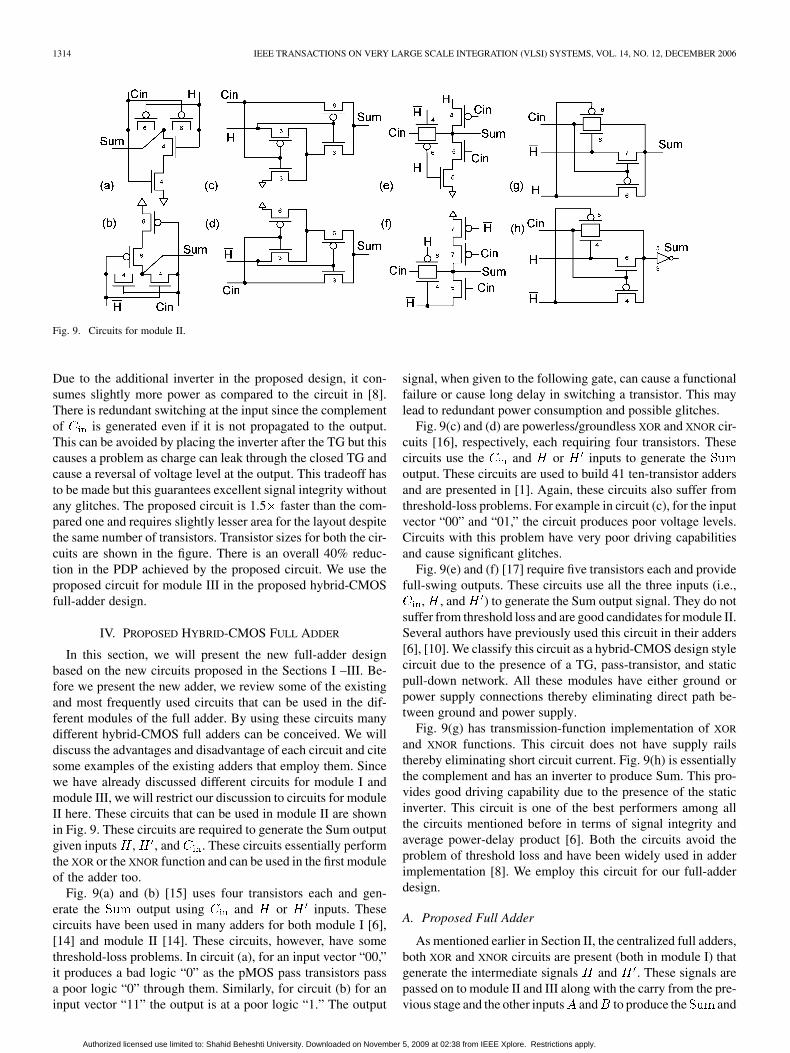
Fig. 9. Circuits for module II.
Due to the additional inverter in the proposed design, it con-sumes slightly more power as compared to the circuit in [8].There is redundant switching at the input since the complementof is generated even if it is not propagated to the output.This can be avoided by placing the inverter after the TG but thiscauses a problem as charge can leak through the closed TG andcause a reversal of voltage level at the output. This tradeoff hasto be made but this guarantees excellent signal integrity withoutany glitches. The proposed circuit is 1.5 faster than the com-pared one and requires slightly lesser area for the layout despitethe same number of transistors. Transistor sizes for both the cir-cuits are shown in the figure. There is an overall 40% reduc-tion in the PDP achieved by the proposed circuit. We use theproposed circuit for module III in the proposed hybrid-CMOSfull-adder design.
IV. PROPOSED HYBRID-CMOS FULL ADDER
In this section, we will present the new full-adder designbased on the new circuits proposed in the Sections I –III. Be-fore we present the new adder, we review some of the existingand most frequently used circuits that can be used in the dif-ferent modules of the full adder. By using these circuits manydifferent hybrid-CMOS full adders can be conceived. We willdiscuss the advantages and disadvantage of each circuit and citesome examples of the existing adders that employ them. Sincewe have already discussed different circuits for module I andmodule III, we will restrict our discussion to circuits for moduleII here. These circuits that can be used in module II are shownin Fig. 9. These circuits are required to generate the Sum outputgiven inputs , , and . These circuits essentially performthe XOR or the XNOR function and can be used in the first moduleof the adder too.
Fig. 9(a) and (b) [15] uses four transistors each and gen-erate the output using and or inputs. Thesecircuits have been used in many adders for both module I [6],[14] and module II [14]. These circuits, however, have somethreshold-loss problems. In circuit (a), for an input vector “00,”it produces a bad logic “0” as the pMOS pass transistors passa poor logic “0” through them. Similarly, for circuit (b) for aninput vector “11” the output is at a poor logic “1.” The output
signal, when given to the following gate, can cause a functionalfailure or cause long delay in switching a transistor. This maylead to redundant power consumption and possible glitches.
Fig. 9(c) and (d) are powerless/groundless XOR and XNOR cir-cuits [16], respectively, each requiring four transistors. Thesecircuits use the and or inputs to generate theoutput. These circuits are used to build 41 ten-transistor addersand are presented in [1]. Again, these circuits also suffer fromthreshold-loss problems. For example in circuit (c), for the inputvector “00” and “01,” the circuit produces poor voltage levels.Circuits with this problem have very poor driving capabilitiesand cause significant glitches.
Fig. 9(e) and (f) [17] require five transistors each and providefull-swing outputs. These circuits use all the three inputs (i.e.,
, , and ) to generate the Sum output signal. They do notsuffer from threshold loss and are good candidates for module II.Several authors have previously used this circuit in their adders[6], [10]. We classify this circuit as a hybrid-CMOS design stylecircuit due to the presence of a TG, pass-transistor, and staticpull-down network. All these modules have either ground orpower supply connections thereby eliminating direct path be-tween ground and power supply.
Fig. 9(g) has transmission-function implementation of XOR
and XNOR functions. This circuit does not have supply railsthereby eliminating short circuit current. Fig. 9(h) is essentiallythe complement and has an inverter to produce Sum. This pro-vides good driving capability due to the presence of the staticinverter. This circuit is one of the best performers among allthe circuits mentioned before in terms of signal integrity andaverage power-delay product [6]. Both the circuits avoid theproblem of threshold loss and have been widely used in adderimplementation [8]. We employ this circuit for our full-adderdesign.
A. Proposed Full Adder
As mentioned earlier in Section II, the centralized full adders,both XOR and XNOR circuits are present (both in module I) thatgenerate the intermediate signals and . These signals arepassed on to module II and III along with the carry from the pre-vious stage and the other inputs and to produce the and
Authorized licensed use limited to: Shahid Beheshti University. Downloaded on November 5, 2009 at 02:38 from IEEE Xplore. Restrictions apply.
GOEL et al.: DESIGN OF ROBUST, ENERGY-EFFICIENT FULL ADDERS 1315
Fig. 10. Proposed hybrid-CMOS full adder.
. For the new adder, we use our two proposed circuits andone existing circuit in the three modules. The proposed adder isshown in Fig. 10.
In module I, the proposed XOR–XNOR circuit produces bal-anced full-swing outputs. It has high-speed operation due tothe cross-coupled pMOS pull-up transistors providing the in-termediate signals quickly. Since the other two modules relyheavily on the intermediate signal and to produce thefinal outputs, the delay response of module I is critical. The pro-posed XOR–XNOR circuit is 1.7 faster than the best availableXOR–XNOR circuits. Due to this reason, the new adder is fasterthan the compared adders.
Module II is a transmission-function implementation of XNOR
function to generate the followed by an inverter to gen-erate . This provides good driving capability to the circuit.Due to the absence of supply rails there are no short circuit cur-rents. The circuit is free from the problem of threshold loss andhas the lowest PDP amongst all circuits that are used for moduleII [6].
Module III employs the proposed hybrid-CMOS output stagewith a static inverter at the output. This circuit has a lower PDPas compared to the other existing designs. The static inverterprovides good driving capabilities as the inputs are decoupledfrom the output. The structure of the circuit is very symmetricand, therefore, the layout is regular. Due to the low PDP ofmodule II and module III, the new adder is expected to havelow power consumption. In Sections V and VI, the simulationenvironment and experimental results will be discussed.
V. SIMULATION ENVIRONMENT
A. Simulation Setup
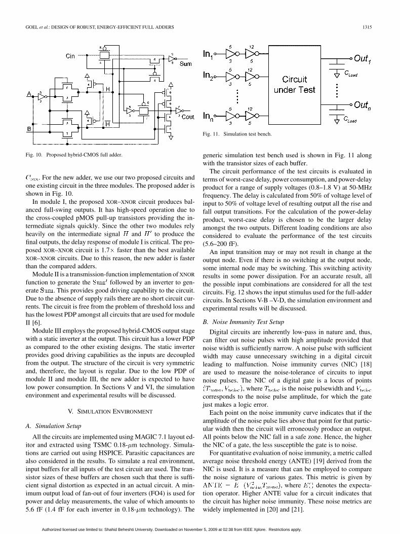
All the circuits are implemented using MAGIC 7.1 layout ed-itor and extracted using TSMC 0.18- m technology. Simula-tions are carried out using HSPICE. Parasitic capacitances arealso considered in the results. To simulate a real environment,input buffers for all inputs of the test circuit are used. The tran-sistor sizes of these buffers are chosen such that there is suffi-cient signal distortion as expected in an actual circuit. A min-imum output load of fan-out of four inverters (FO4) is used forpower and delay measurements, the value of which amounts to5.6 fF (1.4 fF for each inverter in 0.18- m technology). The
Fig. 11. Simulation test bench.
generic simulation test bench used is shown in Fig. 11 alongwith the transistor sizes of each buffer.
The circuit performance of the test circuits is evaluated interms of worst-case delay, power consumption, and power-delayproduct for a range of supply voltages (0.8–1.8 V) at 50-MHzfrequency. The delay is calculated from 50% of voltage level ofinput to 50% of voltage level of resulting output all the rise andfall output transitions. For the calculation of the power-delayproduct, worst-case delay is chosen to be the larger delayamongst the two outputs. Different loading conditions are alsoconsidered to evaluate the performance of the test circuits(5.6–200 fF).
An input transition may or may not result in change at theoutput node. Even if there is no switching at the output node,some internal node may be switching. This switching activityresults in some power dissipation. For an accurate result, allthe possible input combinations are considered for all the testcircuits. Fig. 12 shows the input stimulus used for the full-addercircuits. In Sections V-B –V-D, the simulation environment andexperimental results will be discussed.
B. Noise Immunity Test Setup
Digital circuits are inherently low-pass in nature and, thus,can filter out noise pulses with high amplitude provided thatnoise width is sufficiently narrow. A noise pulse with sufficientwidth may cause unnecessary switching in a digital circuitleading to malfunction. Noise immunity curves (NIC) [18]are used to measure the noise-tolerance of circuits to inputnoise pulses. The NIC of a digital gate is a locus of points
, where is the noise pulsewidth andcorresponds to the noise pulse amplitude, for which the gatejust makes a logic error.
Each point on the noise immunity curve indicates that if theamplitude of the noise pulse lies above that point for that partic-ular width then the circuit will erroneously produce an output.All points below the NIC fall in a safe zone. Hence, the higherthe NIC of a gate, the less susceptible the gate is to noise.
For quantitative evaluation of noise immunity, a metric calledaverage noise threshold energy (ANTE) [19] derived from theNIC is used. It is a measure that can be employed to comparethe noise signature of various gates. This metric is given by
, where denotes the expecta-tion operator. Higher ANTE value for a circuit indicates thatthe circuit has higher noise immunity. These noise metrics arewidely implemented in [20] and [21].
Authorized licensed use limited to: Shahid Beheshti University. Downloaded on November 5, 2009 at 02:38 from IEEE Xplore. Restrictions apply.
1316 IEEE TRANSACTIONS ON VERY LARGE SCALE INTEGRATION (VLSI) SYSTEMS, VOL. 14, NO. 12, DECEMBER 2006
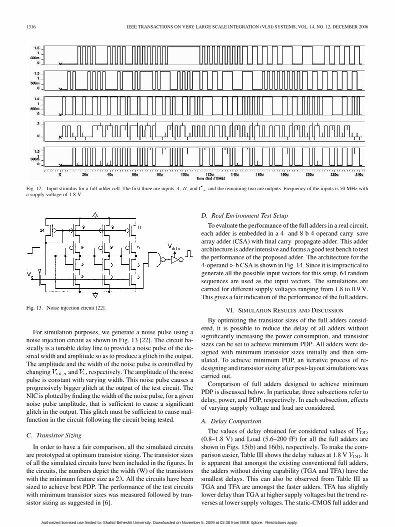
Fig. 12. Input stimulus for a full-adder cell. The first three are inputs A, B, and C and the remaining two are outputs. Frequency of the inputs is 50 MHz witha supply voltage of 1.8 V.
Fig. 13. Noise injection circuit [22].
For simulation purposes, we generate a noise pulse using anoise injection circuit as shown in Fig. 13 [22]. The circuit ba-sically is a tunable delay line to provide a noise pulse of the de-sired width and amplitude so as to produce a glitch in the output.The amplitude and the width of the noise pulse is controlled bychanging and , respectively. The amplitude of the noisepulse is constant with varying width. This noise pulse causes aprogressively bigger glitch at the output of the test circuit. TheNIC is plotted by finding the width of the noise pulse, for a givennoise pulse amplitude, that is sufficient to cause a significantglitch in the output. This glitch must be sufficient to cause mal-function in the circuit following the circuit being tested.
C. Transistor Sizing
In order to have a fair comparison, all the simulated circuitsare prototyped at optimum transistor sizing. The transistor sizesof all the simulated circuits have been included in the figures. Inthe circuits, the numbers depict the width (W) of the transistorswith the minimum feature size as . All the circuits have beensized to achieve best PDP. The performance of the test circuitswith minimum transistor sizes was measured followed by tran-sistor sizing as suggested in [6].
D. Real Environment Test Setup
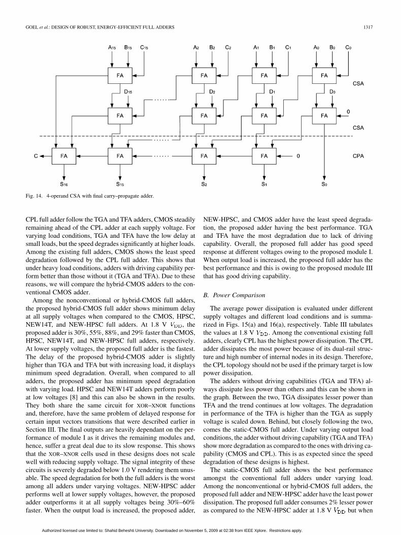
To evaluate the performance of the full adders in a real circuit,each adder is embedded in a 4- and 8-b 4-operand carry–savearray adder (CSA) with final carry–propagate adder. This adderarchitecture is adder intensive and forms a good test bench to testthe performance of the proposed adder. The architecture for the4-operand -b CSA is shown in Fig. 14. Since it is impractical togenerate all the possible input vectors for this setup, 64 randomsequences are used as the input vectors. The simulations arecarried for different supply voltages ranging from 1.8 to 0.9 V.This gives a fair indication of the performance of the full adders.
VI. SIMULATION RESULTS AND DISCUSSION
By optimizing the transistor sizes of the full adders consid-ered, it is possible to reduce the delay of all adders withoutsignificantly increasing the power consumption, and transistorsizes can be set to achieve minimum PDP. All adders were de-signed with minimum transistor sizes initially and then sim-ulated. To achieve minimum PDP, an iterative process of re-designing and transistor sizing after post-layout simulations wascarried out.
Comparison of full adders designed to achieve minimumPDP is discussed below. In particular, three subsections refer todelay, power, and PDP, respectively. In each subsection, effectsof varying supply voltage and load are considered.
A. Delay Comparison
The values of delay obtained for considered values of(0.8–1.8 V) and Load (5.6–200 fF) for all the full adders areshown in Figs. 15(b) and 16(b), respectively. To make the com-parison easier, Table III shows the delay values at 1.8 V . Itis apparent that amongst the existing conventional full adders,the adders without driving capability (TGA and TFA) have thesmallest delays. This can also be observed from Table III asTGA and TFA are amongst the faster adders. TFA has slightlylower delay than TGA at higher supply voltages but the trend re-verses at lower supply voltages. The static-CMOS full adder and
Authorized licensed use limited to: Shahid Beheshti University. Downloaded on November 5, 2009 at 02:38 from IEEE Xplore. Restrictions apply.
GOEL et al.: DESIGN OF ROBUST, ENERGY-EFFICIENT FULL ADDERS 1317
Fig. 14. 4-operand CSA with final carry–propagate adder.
CPL full adder follow the TGA and TFA adders, CMOS steadilyremaining ahead of the CPL adder at each supply voltage. Forvarying load conditions, TGA and TFA have the low delay atsmall loads, but the speed degrades significantly at higher loads.Among the existing full adders, CMOS shows the least speeddegradation followed by the CPL full adder. This shows thatunder heavy load conditions, adders with driving capability per-form better than those without it (TGA and TFA). Due to thesereasons, we will compare the hybrid-CMOS adders to the con-ventional CMOS adder.
Among the nonconventional or hybrid-CMOS full adders,the proposed hybrid-CMOS full adder shows minimum delayat all supply voltages when compared to the CMOS, HPSC,NEW14T, and NEW-HPSC full adders. At 1.8 V , theproposed adder is 30%, 55%, 88%, and 29% faster than CMOS,HPSC, NEW14T, and NEW-HPSC full adders, respectively.At lower supply voltages, the proposed full adder is the fastest.The delay of the proposed hybrid-CMOS adder is slightlyhigher than TGA and TFA but with increasing load, it displaysminimum speed degradation. Overall, when compared to alladders, the proposed adder has minimum speed degradationwith varying load. HPSC and NEW14T adders perform poorlyat low voltages [8] and this can also be shown in the results.They both share the same circuit for XOR–XNOR functionsand, therefore, have the same problem of delayed response forcertain input vectors transitions that were described earlier inSection III. The final outputs are heavily dependant on the per-formance of module I as it drives the remaining modules and,hence, suffer a great deal due to its slow response. This showsthat the XOR–XNOR cells used in these designs does not scalewell with reducing supply voltage. The signal integrity of thesecircuits is severely degraded below 1.0 V rendering them unus-able. The speed degradation for both the full adders is the worstamong all adders under varying voltages. NEW-HPSC adderperforms well at lower supply voltages, however, the proposedadder outperforms it at all supply voltages being 30%–60%faster. When the output load is increased, the proposed adder,
NEW-HPSC, and CMOS adder have the least speed degrada-tion, the proposed adder having the best performance. TGAand TFA have the most degradation due to lack of drivingcapability. Overall, the proposed full adder has good speedresponse at different voltages owing to the proposed module I.When output load is increased, the proposed full adder has thebest performance and this is owing to the proposed module IIIthat has good driving capability.
B. Power Comparison
The average power dissipation is evaluated under differentsupply voltages and different load conditions and is summa-rized in Figs. 15(a) and 16(a), respectively. Table III tabulatesthe values at 1.8 V . Among the conventional existing fulladders, clearly CPL has the highest power dissipation. The CPLadder dissipates the most power because of its dual-rail struc-ture and high number of internal nodes in its design. Therefore,the CPL topology should not be used if the primary target is lowpower dissipation.
The adders without driving capabilities (TGA and TFA) al-ways dissipate less power than others and this can be shown inthe graph. Between the two, TGA dissipates lesser power thanTFA and the trend continues at low voltages. The degradationin performance of the TFA is higher than the TGA as supplyvoltage is scaled down. Behind, but closely following the two,comes the static-CMOS full adder. Under varying output loadconditions, the adder without driving capability (TGA and TFA)show more degradation as compared to the ones with driving ca-pability (CMOS and CPL). This is as expected since the speeddegradation of these designs is highest.
The static-CMOS full adder shows the best performanceamongst the conventional full adders under varying load.Among the nonconventional or hybrid-CMOS full adders, theproposed full adder and NEW-HPSC adder have the least powerdissipation. The proposed full adder consumes 2% lesser poweras compared to the NEW-HPSC adder at 1.8 V but when
Authorized licensed use limited to: Shahid Beheshti University. Downloaded on November 5, 2009 at 02:38 from IEEE Xplore. Restrictions apply.

1318 IEEE TRANSACTIONS ON VERY LARGE SCALE INTEGRATION (VLSI) SYSTEMS, VOL. 14, NO. 12, DECEMBER 2006
Fig. 15. Power, delay, and PDP results for different supply voltages.
the supply voltage is scaled down, NEW-HPSC adder con-sumes slightly lesser power. The performance of these addersremains invariably good under varying voltages and, therefore,they are both suitable for low voltage operation. The powerdissipation of the proposed adder is roughly 25% less than thenext lowest power consuming adder (TGA). With increasingoutput load, the power dissipation of these adders remainsthe least as compared to all the considered full adders. Theremaining two hybrid-CMOS adders (HPSC and NEW14T)
Fig. 16. Power, delay, and PDP results under different load conditions.
show high degradation in performance with decreasing supplyvoltages. Even though they perform well with varying load,they are unsuitable for operation at low voltages.
C. PDP Comparison
The PDP is a quantitative measure of the efficiency of thetradeoff between power dissipation and speed, and is particu-larly important when low-power operation is needed. The valuesof PDP is evaluated under different supply voltages and dif-ferent output loads are summarized in Figs. 15(c) and 16(c),respectively. The PDP curve in Fig. 15(c) has flat minimumfor intermediate values of but the PDP curve for varying
Authorized licensed use limited to: Shahid Beheshti University. Downloaded on November 5, 2009 at 02:38 from IEEE Xplore. Restrictions apply.
GOEL et al.: DESIGN OF ROBUST, ENERGY-EFFICIENT FULL ADDERS 1319
output load follows the same trend as delay and power dissipa-tion curves for varying load.
Among conventional adders, the adders without driving ca-pability (TGA and TFA) have the lowest PDP. The PDP of TFAis lesser than that of TGA for higher voltages but the trend re-verses for lower voltages suggesting that from energy point ofview TGA is a better choice. Among adders with driving capa-bility, the CPL adder as expected has the highest PDP amongstthe conventional adders. The static-CMOS adder has roughly60% lower PDP as compared to the CPL adder for all valuesof supply voltages. Under variable output load conditions, thestatic-CMOS adder shows the least PDP and the least degrada-tion with increasing load rendering it the best amongst the con-ventional full adders. Despite having lowest PDPs, TGA andTFA performances degrade drastically with increasing outputloads. This shows that although these adders show good perfor-mance as standalone units, if cascaded or used in a high fan-outsituation, they may not deliver the required performance. Thisis because the input is not decoupled from the output. In a realcircuit, buffers have to be inserted in between two adders to as-sure good signal strength. This will increase the delay as wellas the power consumption of the whole design.
In the case of nonconventional or hybrid-CMOS adders, theproposed hybrid-CMOS full adder displays the best PDP char-acteristics for both varying supply voltages and output loads.Inverters at the output of module II and module III ensure suffi-cient drive strength. Moreover, the power dissipation result ofthe proposed full adder includes the power consumed by thetwo output inverters, and still is less than other conventional de-signs. When compared to the NEW-HPSC adder, the proposedadder consumes 30% less energy. The number of transistors inthe design is higher than most of the compared adders but it stillprovides better results. This shows that reduction in the numberof transistors is not the only solution to reducing power con-sumption in a circuit. There is roughly 26% reduction in PDPcompared to the TFA that has the lowest among the compareddesigns. The performance of the new full-adder cell is attributedto the proposed XOR–XNOR circuit and the novel hybrid-CMOSoutput module. As shown earlier, these circuits show good im-provement in PDP and are faster compared to their counterparts.The remaining two hybrid-CMOS adders (HPSC and NEW14T)have poor PDP characteristics. For low supply voltages, the PDPrises drastically making them unsuitable for low-voltage opera-tion.
D. Area and Layout Complexity
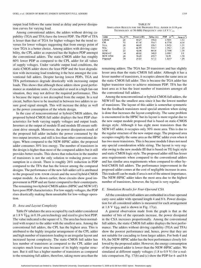
Table IV tabulates the area occupied by each adder consideredat 1.8 V in 0.18- m technology and sized to give best PDP.The value indicated is the square of . The area has been normal-ized with respect to the adder with the smallest area. Among theconventional full adders, the CPL has the highest area. This isattributed to the highly irregular arrangement of the CPL adderand high number of transistors leading to an irregular layout andincreased layout complexity. The static-CMOS full adder hasless number of transistors as compared to the CPL adder andoccupies much lesser area because of its highly regular struc-ture. But it still has a higher number of transistors as comparedto the remaining full adders, therefore, taking more area than the
TABLE IVSIMULATION RESULTS FOR THE PROPOSED FULL ADDER IN 0.18-�m
TECHNOLOGY AT 50-MHZ FREQUENCY AND 1.8 V V
remaining adders. The TGA has 20 transistors and has slightlylesser area than the static-CMOS full adder. Although it has alesser number of transistors, it occupies almost the same area asthe static-CMOS full adder. This is because the TGA adder hashigher transistor sizes to achieve minimum PDP. TFA has theleast area as it has the least number of transistors amongst allthe conventional full adders.
Among the nonconventional or hybrid-CMOS full adders, theNEW14T has the smallest area since it has the lowest numberof transistors. The layout of this adder is somewhat symmetricbut the feedback transistors need special attention when sizingis done that increases the layout complexity. The same problemis encountered in the HPSC but its layout is more regular due tothe new output module proposed that is based on static-CMOSdesign style. Although it has eight more transistors than theNEW14T adder, it occupies only 30% more area. This is due tothe regular structure of the new output stage. The proposed areaoccupies roughly the same area as the HPSC adder even when ithas two more transistors. This is because module I does not needany special consideration while sizing. The layout is very reg-ular owing to the new module III that is based on TG logic styleand static-CMOS logic style. The proposed adder still has lesserarea requirements when compared to the conventional addersand has similar area requirements when compared to other hy-brid-CMOS full adders. The performance improvement in theproposed adder comes at the cost of negligible increase in area.This tradeoff can be made if area is not of the utmost importance.The NEW-HPSC adder takes the most area due to the highestnumber of transistors, however, the layout is very regular.
E. Simulation Results for Four-Operand CSA
All the considered full adders are embedded in a four-operandcarry-save adder with operand length 4 and 8 b. Power dissipa-tion for all considered adders is measured for each arrangementat 1.8 V and is shown in Fig. 17(a).
A general observation made from the graph is that as thenumber of bits of the operands increase, the power dissipatedin the CSA increases proportionally. Among the conventionalfull adders, the static-CMOS full adder displays the best perfor-mance. The adders without driving capability (TGA and TFA)show the poorest performance and, hence, prove that they arenot suitable for cascading to form larger adders. For both 4 and8 b, the NEW-HPSC adder has the best performance closely fol-lowed by the proposed adder. However, the energy consumptionof the proposed adder is lower than the NEW-HPSC adder. Wesimulated at different supply voltages (1.8 to 0.9 V) for a real-istic comparison. Fig. 17(b) and (c) show the PDP for 4- and 8-b
Authorized licensed use limited to: Shahid Beheshti University. Downloaded on November 5, 2009 at 02:38 from IEEE Xplore. Restrictions apply.

1320 IEEE TRANSACTIONS ON VERY LARGE SCALE INTEGRATION (VLSI) SYSTEMS, VOL. 14, NO. 12, DECEMBER 2006
Fig. 17. (a) Power consumption results in the CSA architecture at 1.8 V V .(b) PDP results for 4-b CSA at different supply voltages. (c) PDP results for 8-bCSA.
CSA architectures, respectively. The proposed full adder con-sumes the least energy at voltages other than 1.8 V for both con-figurations. It is closely followed by NEW-HPSC adder whichhas the best results at 1.8 V.
F. Noise Immunity Curves
The noise immunity curves and the ANTE results for theadders are shown in Fig. 18. All the hybrid designs show goodnoise immunity as compared to the standard designs. The HPSCadder has the highest ANTE followed by the NEW-HPSC adder.This shows that more reliable circuits can be designed using hy-brid-CMOS logic design style. Among the nonconventional fulladders, the proposed full adder has the lowest ANTE but it is stillhigher than the conventional full adders.
Fig. 18. (a) Noise immunity curves for the full adders. (b) ANTE results.
VII. CONCLUSION
Hybrid-CMOS design style gives more freedom to thedesigner to select different modules in a circuit dependingupon the application. Using the adder categorization and hy-brid-CMOS design style, many full adders can be conceived.As an example, a novel full adder designed using hybrid-CMOSdesign style is presented in this paper that targets low PDP.The proposed hybrid-CMOS full adder has better performancethan most of the standard full-adder cells owing to the novelsdesign modules proposed in this paper. It performs well withsupply voltage scaling and under different load conditions.When embedded in a four-operand CSA, it outperforms all theother adders making it suitable for larger adders. The proposedadder has better noise immunity as compared to the standardadder such as static CMOS, making it suitable for deep-submi-crometer operation. We recommend the use of hybrid-CMOSdesign style for the design of high-performance circuits.
ACKNOWLEDGMENT
The authors would like to thank the anonymous reviewersfor their constructive critique from which this paper greatlybenefited.
Authorized licensed use limited to: Shahid Beheshti University. Downloaded on November 5, 2009 at 02:38 from IEEE Xplore. Restrictions apply.
GOEL et al.: DESIGN OF ROBUST, ENERGY-EFFICIENT FULL ADDERS 1321
REFERENCES
[1] H. T. Bui, Y. Wang, and Y. Jiang, “Design and analysis of low-power10-transistor full adders using XOR–XNOR gates,” IEEE Trans. CircuitsSyst. II, Analog Digit. Signal Process., vol. 49, no. 1, pp. 25–30, Jan.2002.
[2] V. Tiwari, D. Singh, S. Rajgopal, G. Mehta, R. Patel, and F. Baez, “Re-ducing power in high-performance microprocessors,” in Proc. Conf.Des. Autom., 1998, pp. 732–737.
[3] R. Zimmermann and W. Fichtner, “Low-power logic styles: CMOSversus pass-transistor logic,” IEEE J. Solid-State Circuits, vol. 32, no.7, pp. 1079–1090, Jul. 1997.
[4] N. Zhuang and H. Wu, “A new design of the CMOS full adder,” IEEEJ. Solid-State Circuits, vol. 27, no. 5, pp. 840–844, May 1992.
[5] N. Weste and K. Eshraghian, “Principles of CMOS VLSI design,” in ASystem Perspective. Reading, MA: Addison-Wesley, 1993.
[6] A. M. Shams, T. K. Darwish, and M. A. Bayoumi, “Performance anal-ysis of low-power 1-bit CMOS full adder cells,” IEEE Trans. VeryLarge Scale Integr. (VLSI) Syst., vol. 10, no. 1, pp. 20–29, Feb. 2002.
[7] D. Radhakrishnan, “Low-voltage low-power CMOS full adder,” IEEProc. Circuits Devices Syst., vol. 148, no. 1, pp. 19–24, Feb. 2001.
[8] M. Zhang, J. Gu, and C. H. Chang, “A novel hybrid pass logic withstatic CMOS output drive full-adder cell,” in Proc. IEEE Int. Symp.Circuits Syst., May 2003, pp. 317–320.
[9] C.-H. Chang, J. Gu, and M. Zhang, “A review of 0.18-�m full adderperformances for tree structured arithmetic circuits,” IEEE Trans. VeryLarge Scale Integr. (VLSI) Syst., vol. 13, no. 6, pp. 686–695, Jun. 2005.
[10] M. Sayed and W. Badawy, “Performance analysis of single-bit fulladder cells using 0.18, 0.25, and 0.35 �m CMOS technologies,” inProc. Int. Symp. Circuits Syst., 2002, pp. III-559–III-562.
[11] S. Goel, S. Gollamudi, A. Kumar, and M. Bayoumi, “On the designof low-energy hybrid CMOS 1-bit full-adder cells,” in Proc. MidwestSymp. Circuits Syst., 2004, pp. II-209–212.
[12] H. A. Mahmoud and M. Bayoumi, “A 10-transistor low-power high-speed full adder cell,” in Proc. Int. Symp. Circuits Syst., 1999, pp.I-43–46.
[13] A. Fayed and M. A. Bayoumi, “A low-power 10 transistor full addercell for embedded architectures,” in Proc. IEEE Int. Symp. CircuitsSyst., 2001, pp. IV-226–229.
[14] R. Shalem, L. K. John, and E. John, “A novel low power energy re-covery full adder cell,” in Proc. Great Lake Symp. VLSI, 1999, pp.380–380.
[15] J. Wang, S. Fang, and W. Feng, “New efficient designs for XOR andXNOR functions on the transistor level,” IEEE J. Solid-State Circuits,vol. 29, no. 7, pp. 780–786, Jul. 1994.
[16] H. T. Bui, A. K. Al-Sheraidah, and Y. Wang, “New 4-transistor XOR
and XNOR designs,” in Proc. 2nd IEEE Asia Pacific Conf. ASICs, 2000,pp. 25–28.
[17] H. Lee and G. E. Sobelman, “New low-voltage circuits for XOR andXNOR,” IEEE Proc. Southeastcon., pp. 225–229, 1997.
[18] G. A. Katopis, “Delta-I noise specification for a high-performancecomputing machine,” Proc. IEEE, vol. 73, no. 9, pp. 1405–1415, Sep.1985.
[19] Wang and N. R. Shanbagh, “Noise-tolerant dynamic circuit design,”in Proc. IEEE Int. Symp. Circuits Syst., 1999, pp. 549–552.
[20] S. Goel, M. Elgamel, M. A. Bayoumi, and Y. Hanafy, “Design method-ologies for high-performance noise-tolerant XOR–XNOR circuits,” IEEETrans. Circuits Syst. I, Reg. Papers, vol. 53, no. 4, pp. 867–878, Apr.2006.
[21] S. Goel, T. K. Darwish, and M. A. Bayoumi, “A novel technique fornoise-tolerance in dynamic circuits,” in Proc. IEEE Comput. Soc. Annu.Symp. VLSI, 2003, pp. 203–206.
[22] G. Balamurugan and N. R. Shanbhag, “The twin-transistor noise-tol-erant dynamic circuit technique,” IEEE J. Solid-State Circuits, vol. 36,no. 2, pp. 273–280, Feb. 2001.
Sumeer Goel (S’01) obtained a B.Tech. degree inelectronics and communications engineering fromPunjab Technical University, Jalandar, India, in2001, and the M.S. degree in computer engineeringfrom The Center for Advanced Computer Studies(CACS), University of Louisiana at Lafayette,Lafayette, in 2003, where he is currently pursuingthe Ph.D. degree.
His research interests include high-performancedigital circuit design, algorithms, and VLSI archi-tectures for video processing with a focus on motion
estimation algorithms. At the circuit level, he has also devised methods fornoise reduction, which appeared in the IEEE TRANSACTIONS ON CIRCUITS AND
SYSTEMS (TCAS-I) in April 2006. He is currently the President of the IEEEComputer Society student chapter at the University of Louisiana at Lafayette.
Mr. Goel is the recipient of two Best Student Paper Awards and was alsonominated in the Ten Best Papers at the IEEE-MWSCAS in 2005.
Ashok Kumar (S’98–M’99–SM’06) received theB.Tech. degree in computer science and engineeringfrom the Institute of Technology, BHU Varanasi,India, in 1990, and the M.S. and Ph.D. degreesfrom the Center for Advanced Computer Studies(CACS) at the University of Louisiana at Lafayette,Lafayette, in 1997 and 1999, respectively.
Currently, he is a member of the Research Facultyat CACS. From 1990 to 1994, he worked as an Engi-neer and a Senior Engineer with Uptron India Lim-ited, Lucknow, India. After getting his Ph.D. degree,
he worked with Cadence Design Systems, Lowell/Chemsford, MA, for nearlyfour years as a Senior Member of Technical Staff for Research and Developmentoperations. His research interests include power and noise efficient circuit de-sign, development of algorithms for computer-aided design (CAD) tools, digitalsignal processing, energy-efficient wireless sensor networks, and their deploy-ment. He has served on the program committees of eight conferences as well ason the proposal-evaluation committees of the National Science Foundation.
Magdy A. Bayoumi (S’80–M’84–SM’87–F’99)received the B.Sc. and M.Sc. degrees in electricalengineering from Cairo University, Cairo, Egypt,the M.Sc. degree in computer engineering fromWashington University, St. Louis, and the Ph.D.degree in electrical engineering from the Universityof Windsor, Windsor, ON, Canada.
He has been a faculty member of the Universityof Louisiana at Lafayette since 1985, where he isthe Director of the Center for Advanced ComputerStudies (CACS), Department Head of the Computer
Science Department, the Edmiston Professor of Computer Engineering, and theLamson Professor of Computer Science at the Center for Advanced ComputerStudies. His research interests include VLSI design methods and architectures,low power circuits and systems, digital signal processing architectures, parallelalgorithm design, computer arithmetic, image and video signal processing,neural networks, and wideband network architectures. He was the Vice Pres-ident for the technical activities of the IEEE Circuits and Systems Society.He is the chairman of the Technical Committee on Circuits and Systems forCommunication and the TC on Signal Processing Design and Implementation.He was a founding member and the chairman of the VLSI Systems andApplications Technical Committee. He is a member of the Neural Networkand the Multimedia Technology Technical Committees. He has been on theTechnical Program Committee for ISCAS for several years, and he was thePublication Chair for ISCAS’99. He was the General Chairman of the 1994MWSCAS and he is a member of the Steering Committee of this symposium.He was an Associate Editor of the IEEE Circuits and Devices Magazine, theIEEE TRANSACTIONS ON VERY LARGE SCALE INTEGRATION (VLSI) SYSTEMS,the IEEE TRANSACTIONS ON NEURAL NETWORKS, and the Transaction onCircuits and Systems II. He was the co-chairman of the Workshop on ComputerArchitecture for Machine Perception in 1993 and is a member of the SteeringCommittee of this workshop. He was the General Chairman for the 8th GreatLake Symposium on VLSI in 1998. He was also the General Chairman ofthe 2000 Workshop on Signal Processing Design and Implementation. Dr.Bayoumi is an Associate Editor of Integration, the VLSI Journal, and theJournal of VLSI Signal Processing Systems. He is a regional Editor for the VLSIDesign Journal and on the Advisory Board of the Journal on MicroelectronicsSystems Integration. He has edited and co-edited three books in the area ofVLSI signal processing. He served on the Distinguished Visitors Program forthe IEEE Computer Society from 1991 to 1994 and he is on the DistinguishedLecture program of the Circuits and Systems society. He is the faculty advisorfor the IEEE Computer student chapter at UL Lafayette.
Dr. Goel is the recipient of the UL Lafayette 1988 Researcher of the YearAward and the 1993 Distinguished Professor Award at UL Lafayette.
Authorized licensed use limited to: Shahid Beheshti University. Downloaded on November 5, 2009 at 02:38 from IEEE Xplore. Restrictions apply.