
Design of Programmable Baseband Processors
151
Linköping Studies in Science and Technology Dissertation No. 969 Design of Programmable Baseband Processors Eric Tell Cover image Department of Electrical Engineering Linköping University SE-581 83 Linköping, Sweden Linköping 2005
Transcript of Design of Programmable Baseband Processors

Linköping Studies in Science and TechnologyDissertation No. 969
Design of ProgrammableBaseband Processors
Eric Tell
Cover image
Department of Electrical EngineeringLinköping University
SE-581 83 Linköping, Sweden
Linköping 2005

Linköping Studies in Science and TechnologyDissertation No. 969
Design of ProgrammableBaseband Processors
Eric Tell
Department of Electrical EngineeringLinköping University
SE-581 83 Linköping, Sweden
Linköping 2005
ISBN 91-85457-20-5ISSN 0345-7524
ii
Design of ProgrammableBaseband ProcessorsEric TellISBN 91-85457-20-5
Copyright c© Eric Tell, 2005
Linköping Studies in Science and TechnologyDissertation No. 969ISSN 0345-7524
Department of Electrical EngineeringLinköping UniversitySE-581 83 LinköpingSwedenPhone: +46 13 28 10 00
Author e-mail: [email protected]
Cover imageVisualization of the BBP1 architecture. Data memories and ac-celerator blocks are connected to the central DSP core via aconfigurable network. The image has been generated usingPOV-Ray 3.5.
Printed by UniTryck, Linköping UniversityLinköping, Sweden, 2005

Abstract
The world of wireless communications is under constant change. Radiostandards evolve and new standards emerge. More and more function-ality is put into wireless terminals. E.g. a mobile phone needs to handleboth second and third generation mobile telephony as well as Bluetooth,and will soon also support wireless LAN functionality, reception of digitalaudio and video broadcasting, etc.
These developments have lead to an increased interest in software de-fined radio (SDR), i.e. radio devices that can be reconfigured via software.SDR would provide benefits such as low cost for multi-mode devices,reuse of the same hardware in different products, and increased productlife time via software updates.
One essential part of any software defined radio is a programmablebaseband processor that is flexible enough to handle different types ofmodulation, different channel coding schemes, and different tradeoffs be-tween data rate and mobility.
So far, programmable baseband solutions have mostly been used inhigh end systems such as mobile telephony base stations since the costand power consumption have been considered too high for handheld ter-minals.
In this work a new low power and low silicon area programmablebaseband processor architecture aimed for multi-mode terminals is pre-sented. The architecture is based on a customized DSP core and a num-ber of hardware accelerators connected via a configurable network. Thearchitecture offers a good tradeoff between flexibility and performance
iii

iv Abstract
through an optimized instruction set, efficient hardware acceleration ofcarefully selected functions, low memory cost, and low control overhead.
One main contribution of this work is a study of important issues inprogrammable baseband processing such as software-hardware partition-ing, instruction level acceleration, low power design, and memory issues.Further contributions are a unique optimized instruction set architecture,a unique architecture for efficient integration of hardware accelerators inthe processor, and mapping of complete baseband applications to the pre-sented architecture.
The architecture has been proven in a manufactured demonstratorchip for WLAN applications. WLAN firmware has been developed andrun on the chip at full speed. Silicon area and measured power consump-tion have proven to be similar to that of a non-programmable ASIC solu-tion.

Preface
The contents of this thesis present the research that I have done duringthe last 4 years. Various parts of the presented architecture have beendescribed in the following conference papers:
• Eric Tell, Anders Nilsson, and Dake Liu, “A Low Power and LowArea Programmable Baseband Processor Architecture”, in Proceed-ings of the 5th International Workshop on System-on-chip for Real-TimeApplications (IWSOC), Banff, Canada, July 2005
• Eric Tell, Anders Nilsson, and Dake Liu, “A Programmable DSPCore for Baseband Processing”, in Proceedings of the IEEE NortheastWorkshop on Circuits and Systems (NEWCAS), Quebec City, Canada,June 2005
• Eric Tell, Anders Nilsson, and Dake Liu, “Implementation of a Pro-grammable Baseband Processor”, in Proceedings of Radiovetenskapoch Kommunikation (RVK), Linköping, Sweden, June 2005
• Eric Tell and Dake Liu, “A hardware architecture for a multi-modeblock interleaver”, in Proceedings of the International Conference on cir-cuits and systems for communications (ICCSC), Moscow, Russia, July2004
• Eric Tell, Mikael Olausson, and Dake Liu, “A General DSP proces-sor at the cost of 23k gates and 1/2 a man-year design time”, in Pro-ceedings of the International Conference on Acoustics, Signal and SpeechProcessing (ICASSP), Hong Kong, April 2003
v

vi Preface
• Anders Nilsson, Eric Tell, and Dake Liu, “An accelerator architec-ture for programmable multi-standard baseband processors”, in Pro-ceedings of the International Conference on Wireless Networks and Emerg-ing Technologies (WNET), Banff, Canada, July 2004
Some early parts of my work are covered in the following book chapter:
• Dake Liu and Eric Tell, “Chapter 23 - Low Power ProgrammableBaseband Processors”, in Low Power Electronics Design, editor Chris-tian Piguet, CRC Press, July 2004
The following draft journal manuscript is a work in progress:
• Eric Tell, Anders Nilsson, and Dake Liu, “Low Area and Low PowerProgrammable Baseband Processing”, to be sumitted
The following papers are also more or less related to the presented work:
• Eric Tell, Olle Seger, and Dake Liu, “A converged hardware solu-tion for FFT, DCT, and Walsh transform”, in Proceedings of the Inter-national Symposium on Signal Processing and its Applications (ISSPA),Paris, France, July 2003
• Eric Tell and Dake Liu, “A Suitable Channel Equalization Schemefor IEEE 802.11b”, in Proceedings of the Swedish system-on-chip confer-ence (SSoCC), Eskilstuna, Sweden, April 2003
• Anders Nilsson, Eric Tell, and Dake Liu, “Design Methodology formemory-efficient multi-standard baseband processors”, in Proceed-ings of the Asia-Pacific Communications Conference (APCC), Perth, Aus-tralia, October 2005
• Anders Nilsson, Eric Tell, and Dake Liu, “A Programmable SIMD-based Multi-standard Rake-receiver Architecture”, in Proceedings ofEuropean Signal Processing Conference (EUSIPCO), Antalya, Turkey,August 2005

Preface vii
• Anders Nilsson, Eric Tell, and Dake Liu, “A fully programmablerake-receiver architecture for multi-standard baseband processing”,in Proceedings of the International Conference on Networks and Commu-nication Systems (NCS), Krabi, Thailand, May 2005
• Dake Liu, Eric Tell, Anders Nilsson, and Ingemar Söderquist, “Fullyflexible baseband DSP processors for future SDR/JTRS”, in Proceed-ings of Western European Armaments Organization CEPA2 Workshop,Brussels, Belgium, March 2005
• Dake Liu, Eric Tell, and Anders Nilsson, “Implementation of Pro-grammable Baseband Processors”, in Proceedings of CCIC, Hangzhou,China, November 2004
• Haiyan Jiao, Anders Nilsson, Eric Tell, and Dake Liu, “MIPS costestimation for OFDM-VBLAST systems”, submitted conference pa-per

viii Preface
Acknowledgments
There are many people who deserve my gratitude for their contributionsto my research and for making my time as a PhD student so enjoyable. Iwould especially like to thank the following:
• My supervisor professor Dake Liu, for accepting me as his PhD stu-dent, for coming up with the idea for this project, and for supportand encouragement.
• My closest cooperator Lic. Eng. Anders Nilsson, for many fruitfuldiscussions over the last two years as well as more concrete helpwith coding, baseband algorithm development, and PCB design.
• Dr. Olle Seger for sharing his expertise in signal processing.
• Dr. Anders Edman for interesting discussions and ideas.
• My former and current fellow PhD students at Computer Engineer-ing: Dr. Daniel Wiklund, Dr. Thomas Henriksson, Dr. Ulf Nord-qvist, Lic. Eng. Mikael Olausson, Andreas Ehliar, Johan Eilert, PerKarlsson, and Di Wu. Special thanks to Daniel for proofreading mydissertation.
• Anders Edqvist for a good job on the C-compiler for the BBP1 pro-cessor.
• ICC Shanghai for help with chip back-end work and fabrication.
ix

x Acknowledgments
• Ylva Jernling for making all administrative tasks so simple and An-ders Nilsson (Sr) for technical support.
• The rest of the Computer Engineering group, for providing a pleas-ant working environment.
• And finally, my parents for always supporting me and Lena for in-spiration as well as much needed distraction from work.
This research was funded by the Socware program.
Eric TellLinköping, August 2005

Contents
Abstract iii
Preface v
Acknowledgments ix
List of Figures xvii
List of Tables xix
Abbreviations xxi
I Background 1
1 Introduction 31.1 Background . . . . . . . . . . . . . . . . . . . . . . . . . . . 31.2 Scope of the Thesis . . . . . . . . . . . . . . . . . . . . . . . 4
1.3 Contributions . . . . . . . . . . . . . . . . . . . . . . . . . . 5
1.4 Organization of the Thesis . . . . . . . . . . . . . . . . . . . 6
2 Multi-standard Radio Systems and Software Defined Radio 72.1 Trends in Wireless Systems and Devices . . . . . . . . . . . 7
2.2 Software Defined Radio . . . . . . . . . . . . . . . . . . . . 82.3 JTRS and SCA . . . . . . . . . . . . . . . . . . . . . . . . . . 11
Bibliography . . . . . . . . . . . . . . . . . . . . . . . . . . . . . . 12
xi
xii Contents
II Design of Programmable Baseband Processors 13
3 Application Specific Processors 153.1 Introduction . . . . . . . . . . . . . . . . . . . . . . . . . . . 153.2 Acceleration Techniques . . . . . . . . . . . . . . . . . . . . 17
3.2.1 Instruction Level Acceleration . . . . . . . . . . . . 183.2.2 Special Addressing . . . . . . . . . . . . . . . . . . . 193.2.3 Function Level Acceleration . . . . . . . . . . . . . . 19
3.3 Design Flow . . . . . . . . . . . . . . . . . . . . . . . . . . . 203.3.1 Requirement Specification . . . . . . . . . . . . . . . 203.3.2 Behavior Modeling . . . . . . . . . . . . . . . . . . . 213.3.3 Initial Architecture Plan and MIPS Estimation . . . 233.3.4 Instruction Set Design and Architecture Planning . 233.3.5 Instruction Set Simulator . . . . . . . . . . . . . . . 243.3.6 Benchmarking and Profiling . . . . . . . . . . . . . 253.3.7 Acceleration . . . . . . . . . . . . . . . . . . . . . . . 263.3.8 Architecture Design . . . . . . . . . . . . . . . . . . 273.3.9 RTL Implementation and Backend Flow . . . . . . . 283.3.10 Verification . . . . . . . . . . . . . . . . . . . . . . . 283.3.11 Concluding Remarks . . . . . . . . . . . . . . . . . . 29
3.4 Processor Tool Chain . . . . . . . . . . . . . . . . . . . . . . 303.5 Low Power Design . . . . . . . . . . . . . . . . . . . . . . . 30
3.5.1 Operand Stopping . . . . . . . . . . . . . . . . . . . 313.5.2 Memory . . . . . . . . . . . . . . . . . . . . . . . . . 313.5.3 Control Overhead . . . . . . . . . . . . . . . . . . . 323.5.4 Leakage . . . . . . . . . . . . . . . . . . . . . . . . . 323.5.5 Acceleration and Parallelism . . . . . . . . . . . . . 323.5.6 Data Width Masking . . . . . . . . . . . . . . . . . . 33
Bibliography . . . . . . . . . . . . . . . . . . . . . . . . . . . . . . 34
4 Introduction to Baseband Processing 374.1 System Overview . . . . . . . . . . . . . . . . . . . . . . . . 374.2 The Transmitter . . . . . . . . . . . . . . . . . . . . . . . . . 384.3 The Receiver . . . . . . . . . . . . . . . . . . . . . . . . . . . 40

Contents xiii
4.3.1 Dynamic Range . . . . . . . . . . . . . . . . . . . . . 40
4.3.2 Synchronization . . . . . . . . . . . . . . . . . . . . . 41
4.3.3 Channel Estimation and Equalization . . . . . . . . 41
4.3.4 Frequency and Timing Offset . . . . . . . . . . . . . 42
4.3.5 Mobility . . . . . . . . . . . . . . . . . . . . . . . . . 42
4.3.6 Demodulation and Channel Decoding . . . . . . . . 43
4.4 OFDM Modulation . . . . . . . . . . . . . . . . . . . . . . . 43
4.5 Spread Spectrum Modulation . . . . . . . . . . . . . . . . . 44
4.6 MIMO Systems . . . . . . . . . . . . . . . . . . . . . . . . . 46
4.7 Computational Complexity . . . . . . . . . . . . . . . . . . 46
Bibliography . . . . . . . . . . . . . . . . . . . . . . . . . . . . . . 48
5 Programmable Baseband Processors 51
5.1 Introduction . . . . . . . . . . . . . . . . . . . . . . . . . . . 51
5.2 Processing Requirements . . . . . . . . . . . . . . . . . . . . 51
5.2.1 Convolution-Based Complex-Valued Processing . . 52
5.2.2 Bit-Based Processing . . . . . . . . . . . . . . . . . . 53
5.2.3 Error Correction . . . . . . . . . . . . . . . . . . . . 53
5.3 Real-Time Requirements . . . . . . . . . . . . . . . . . . . . 54
5.4 Memory Issues . . . . . . . . . . . . . . . . . . . . . . . . . 55
Bibliography . . . . . . . . . . . . . . . . . . . . . . . . . . . . . . 56
6 Related Work 57
6.1 Introduction . . . . . . . . . . . . . . . . . . . . . . . . . . . 57
6.2 Rice University - Imagine . . . . . . . . . . . . . . . . . . . 57
6.3 Morpho Technologies - M-rDSP . . . . . . . . . . . . . . . . 58
6.4 Sandbridge Technologies - Sandblaster . . . . . . . . . . . . 58
6.5 SystemOnIC - Hipersonic . . . . . . . . . . . . . . . . . . . 59
6.6 Other Solutions . . . . . . . . . . . . . . . . . . . . . . . . . 59
6.7 Discussion . . . . . . . . . . . . . . . . . . . . . . . . . . . . 60
Bibliography . . . . . . . . . . . . . . . . . . . . . . . . . . . . . . 61
xiv Contents
III The BBP1 Architecture 63
7 The BBP1 Baseband Processor Architecture 657.1 Introduction . . . . . . . . . . . . . . . . . . . . . . . . . . . 657.2 Architecture Overview . . . . . . . . . . . . . . . . . . . . . 66
7.2.1 The Network . . . . . . . . . . . . . . . . . . . . . . 687.2.2 The DSP Core . . . . . . . . . . . . . . . . . . . . . . 687.2.3 The MAC Unit . . . . . . . . . . . . . . . . . . . . . 71
7.3 Vector Instructions . . . . . . . . . . . . . . . . . . . . . . . 727.4 The Accelerator Network . . . . . . . . . . . . . . . . . . . 76
7.4.1 Accelerator Chaining and Function Level Pipelining 777.5 Data Memory Architecture . . . . . . . . . . . . . . . . . . . 78
7.5.1 Address Generation . . . . . . . . . . . . . . . . . . 797.6 Function Level Acceleration for BBP1 . . . . . . . . . . . . 80
7.6.1 Channel Coding . . . . . . . . . . . . . . . . . . . . 817.6.2 Scrambling . . . . . . . . . . . . . . . . . . . . . . . 817.6.3 Interleaving . . . . . . . . . . . . . . . . . . . . . . . 817.6.4 Demapping . . . . . . . . . . . . . . . . . . . . . . . 827.6.5 Walsh Transform . . . . . . . . . . . . . . . . . . . . 827.6.6 CRC . . . . . . . . . . . . . . . . . . . . . . . . . . . 827.6.7 Front-End Accelerator . . . . . . . . . . . . . . . . . 82
7.7 Design Variations and Scalability Issues . . . . . . . . . . . 837.7.1 Scalability - Increasing Computing Capacity . . . . 837.7.2 Simultaneous Multi-Standard Processing . . . . . . 847.7.3 The Network . . . . . . . . . . . . . . . . . . . . . . 85
Bibliography . . . . . . . . . . . . . . . . . . . . . . . . . . . . . . 86
8 Implementation 898.1 Introduction . . . . . . . . . . . . . . . . . . . . . . . . . . . 898.2 Design Tools . . . . . . . . . . . . . . . . . . . . . . . . . . . 89
8.2.1 The Assembler . . . . . . . . . . . . . . . . . . . . . 898.2.2 The Instruction Set Simulator . . . . . . . . . . . . . 90
8.3 Firmware . . . . . . . . . . . . . . . . . . . . . . . . . . . . . 938.4 Prototype Chip . . . . . . . . . . . . . . . . . . . . . . . . . 94

Contents xv
8.5 Test Board and Measurement Setup . . . . . . . . . . . . . 97Bibliography . . . . . . . . . . . . . . . . . . . . . . . . . . . . . . 97
IV Conclusions and Future Work 99
9 Conclusions 1019.1 Issues in Design of Programmable Baseband Processors . . 1019.2 An Architecture for Efficient Baseband Processing . . . . . 1039.3 Implementation Results . . . . . . . . . . . . . . . . . . . . 103
10 Future Work 10510.1 ISA Improvements . . . . . . . . . . . . . . . . . . . . . . . 10510.2 Architecture Scaling . . . . . . . . . . . . . . . . . . . . . . . 10510.3 Acceleration . . . . . . . . . . . . . . . . . . . . . . . . . . . 10610.4 Low-Power Features . . . . . . . . . . . . . . . . . . . . . . 10610.5 Hardware . . . . . . . . . . . . . . . . . . . . . . . . . . . . 10610.6 Firmware Design Tools . . . . . . . . . . . . . . . . . . . . . 107Bibliography . . . . . . . . . . . . . . . . . . . . . . . . . . . . . . 107
V Appendix 109
A Application Profiling and Benchmarking 111Bibliography . . . . . . . . . . . . . . . . . . . . . . . . . . . . . . 115
B Scheduling and Hardware Allocation 117B.1 The SIFS . . . . . . . . . . . . . . . . . . . . . . . . . . . . . 117B.2 IEEE 802.11a . . . . . . . . . . . . . . . . . . . . . . . . . . . 118B.3 IEEE 802.11b . . . . . . . . . . . . . . . . . . . . . . . . . . . 119Bibliography . . . . . . . . . . . . . . . . . . . . . . . . . . . . . . 124
Index 125

xvi Contents

List of Figures
3.1 Flexibility vs. performance/power . . . . . . . . . . . . . . 163.2 Methods for increasing performance . . . . . . . . . . . . . 173.3 A simplified view of the ASIP design flow . . . . . . . . . . 21
4.1 Overview of a radio transceiver . . . . . . . . . . . . . . . . 374.2 Overview of baseband processing . . . . . . . . . . . . . . . 384.3 Examples of signal constellations . . . . . . . . . . . . . . . 394.4 OFDM processing flows . . . . . . . . . . . . . . . . . . . . 454.5 DSSS/CDMA processing flows . . . . . . . . . . . . . . . . 474.6 Data rate and mobility for different standards . . . . . . . . 48
7.1 Overview of the BBP1 architecture . . . . . . . . . . . . . . 677.2 Instruction encoding formats . . . . . . . . . . . . . . . . . 697.3 The control path . . . . . . . . . . . . . . . . . . . . . . . . . 707.4 The MAC unit . . . . . . . . . . . . . . . . . . . . . . . . . . 737.5 Fraction of the execution clock cycles spent on vector in-
structions and other instructions . . . . . . . . . . . . . . . 747.6 Illustration of instruction parallelism. FFT.64 and SQRAB-
SMAX.64 are vector instructions . . . . . . . . . . . . . . . 747.7 Timing for execution of the instructions in the code exam-
ple from figure 7.6 . . . . . . . . . . . . . . . . . . . . . . . . 757.8 Network transaction examples . . . . . . . . . . . . . . . . 777.9 Function level pipelining . . . . . . . . . . . . . . . . . . . . 787.10 Combined IEEE 802.11a/b scrambler/descrambler . . . . . 81
xvii

xviii List of Figures
8.1 Organization of the instruction set simulator . . . . . . . . 918.2 Simulator execution flow chart . . . . . . . . . . . . . . . . 928.3 Die photo . . . . . . . . . . . . . . . . . . . . . . . . . . . . . 96
B.1 Scheduling of IEEE 802.11a receiver for 160 MHz clock fre-quency . . . . . . . . . . . . . . . . . . . . . . . . . . . . . . 120
B.2 Scheduling of IEEE 802.11b preamble and header process-ing for 154 MHz clock frequency . . . . . . . . . . . . . . . 121
B.3 Scheduling of IEEE 802.11b 2 Mbit/s reception . . . . . . . 122B.4 Scheduling of IEEE 802.11b 11 Mbit/s reception . . . . . . 123

List of Tables
3.1 Relative dynamic power consumption using data maskingand reduced hardware precision. . . . . . . . . . . . . . . . 34
7.1 Examples of vector instructions . . . . . . . . . . . . . . . . 76
8.1 Firmware implementation results . . . . . . . . . . . . . . . 948.2 Chip feature summary . . . . . . . . . . . . . . . . . . . . . 958.3 Chip area usage . . . . . . . . . . . . . . . . . . . . . . . . . 96
A.1 Summary of IEEE 802.11a/b receiver processing . . . . . . 112A.2 IEEE 802.11a/b MIPS costs at highest data rates . . . . . . 113A.3 Cycle cost for IEEE 802.11a kernel operations . . . . . . . . 115
xix

xx List of Tables

Abbreviations
3G Third generation mobile telecommunicationADC Analog to digital converter or conversionAFC Automatic frequency controlAGC Automatic gain controlASIC Application specific integrated circuitBPSK Binary phase shift keyingCCK Complementary code keyingCDMA Code division multiple accessDAB Digital audio broadcastingDAC Digital to analog converter or conversionDBPSK Differential binary phase shift keyingDQPSK Differential quadrature phase shift keyingDSP Digital signal processor or processingDSSS Direct sequence spread spectrumDVB Digital video broadcastingFIR Finite impulse responseFPGA Field programmable gate arrayGPS Global positioning systemHDL Hardware description languageIDE Integrated design environmentIP Intellectual PropertyISA Instruction set architectureISI Inter-symbol interference
xxi

xxii Abbreviations
ISS Instruction set simulatorJTC Joint Technical CommitteeGUI Graphical user interfaceMAC Multiply-accumulate or Media access controlMIMO Multiple input multiple outputMIPS Million instructions per secondmodem Modulator-demodulatorOFDM Orthogonal frequency division multiplexingPC Program counterPHY Physical layerQAM Quadrature amplitude modulationQPSK Quadrature phase shift keyingRISC Reduced instruction set computerRTL Register transfer levelSDR Software defined radioSDRF Software defined radio forumSIFS Short intra-frame spacingSIMD Single instruction multiple dataSNR Signal-to-noise ratioUMTS Universal mobile telephony systemVLIW Very long instruction wordWCDMA Wideband CDMAWLAN Wireless local area network

Part I
Background
1


Chapter 1
Introduction
1.1 Background
The evolution of wireless devices and systems is not slowing down. Newstandards keep coming up in cellular telephony, wireless computer net-works, and audio/video broadcasting. Another trend is convergence ofwireless devices. In other words, more and more functions are put intowireless terminals. A device such as a mobile phone has to handle multi-ple radio standards: both second and third generation mobile telephonyas well as Bluetooth are becoming mandatory. Many devices will in ad-dition support networking standards such as WiFi and WiMax, receptionof broadcast radio and television, and possibly GPS.
This has lead to an increased interest in the concept of Software De-fined Radio (SDR). The idea is that it should be possible to alter the func-tionality of a radio device at run-time by simply replacing its software.This means that the same hardware should be able to handle many differ-ent frequency bands and modulation types as well as different demandson data rate and mobility. This would make it possible for manufactur-ers to reuse the same hardware for different products and ultimately forusers to connect to any system that happens to be available at any giventime and place.
One important component in any modern radio device is the modem
3

4 Introduction
(modulator/demodulator) or baseband processor which handles the heavydigital signal processing required in the physical layer (PHY) of the radiosystem. In order to realize SDR, a programmable baseband processor isneeded.
Although SDR has been discussed for many years, it is still only usedto some extent in large, high-cost components such as mobile telephonybase stations and military systems. In these systems, the SDR functional-ity is typically handled by standard DSP processors or FPGA-type solu-tions.
One reason why SDR has not yet had a breakthrough is that it hasbeen considered to expensive and power consuming for handheld, bat-tery powered devices. In order to achieve the low cost and power con-sumption required for such devices, the baseband processor must be opti-mized for the types of operations that are needed in baseband processing.
Existing processors for SDR tend to be based on traditional architec-tures where the required computing capacity is reached by e.g. traditionalVLIW and SIMD solutions. This usually leads to solutions which are tooarea and power consuming for many applications. New architectures areneeded.
With this background, a research project on programmable basebandprocessing was started at the Computer Engineering group at LinköpingUniversity in the spring of 2002. This thesis is one result of that project.
1.2 Scope of the Thesis
The goal of the research project has been to find new efficient architecturesfor programmable baseband processing. The focus has been on wirelessterminals, implying that features such as low cost and low power con-sumption are essential.
The central part of the thesis is the presentation of the baseband pro-cessor architecture which is the main result of the work in this project.It also describes the implementation of a demonstrator chip, mainly fo-cused on Wireless LAN (WLAN) applications, and the implementation of

1.3 Contributions 5
WLAN standards on this chip.
This thesis also includes an introduction to design of application spe-cific processors and an overview of baseband processing tasks and chal-lenges. General ideas for design of efficient programmable baseband pro-cessors are also discussed.
A discussion of the design approach as well as experiences and conclu-sions made during the design work is also presented. Some parts regard-ing e.g. acceleration techniques and low-power issues are not basebandspecific but valid for application specific processors in general.
1.3 Contributions
The main contributions of the presented work can be summarized in thefollowing three points:
• Review of important issues in programmable baseband processingsuch as SW-HW partitioning, instruction level acceleration, memoryissues, and low power design, and their impact in this specific case.
• Development and demonstration of an area and power efficient ar-chitecture for baseband processing . This includes design of an in-struction set including a new type of instructions operating of vec-tors of complex numbers and a scheme for integrating hardware ac-celeration blocks with the programmable DSP core. The feasibilityof the architecture as well as low silicon area and power consump-tion has been proven by measurements on a manufactured demon-strator chip.
• Mapping of baseband applications to the proposed architecture. TheWLAN standards IEEE 802.11a and IEEE 802.11b has been sched-uled onto the processor. Firmware has been developed and demon-strated on the manufactured chip, proving the correctness of thehardware and that the programmable architecture can meet the re-quirements and challenges in radio baseband processing.
6 Introduction
Although not presented in this thesis, significant work has also beenput into investigating and evaluating various baseband processing algo-rithms from the perspectives of performance and suitability for softwareimplementation.
1.4 Organization of the Thesis
The thesis is divided into four parts. The first part contains the introduc-tion and a short background on SDR.
The second part of the thesis contains an introduction to design ofapplication specific processors in chapter 3 and an introduction to base-band processing in chapter 4. It also provides a short general discussionabout issues in programmable baseband processors in chapter 5 and abrief overview of existing solutions in chapter 6.
The third part is the core of the thesis. Chapter 7 presents the proposedprocessor architecture in general and chapter 8 describes the implementa-tion of a demonstrator chip as well as firmware design and design tools.
The last part contains conclusions in chapter 9 and directions andideas for future work in chapter 10.
Some additional details regarding application profiling, benchmark-ing, hardware mapping, and scheduling for WLAN standards are foundin appendices.

Chapter 2
Multi-standard RadioSystems and Software
Defined Radio
2.1 Trends in Wireless Systems and Devices
The constant change in the world of wireless systems and the increasingconvergence of wireless devices was touched upon already in the intro-duction of this thesis. Wireless devices like mobile phones (or their futureequivalent) will need to handle an increasing amount of different func-tions. The processing requirements of modern standards are increasingdue to increased bandwidth in combination with high mobility. At thesame time power consumption continues to be very important for batterypowered devices.
The amount of upcoming standards and the constant demand for newfeatures and short development time increase the benefits of program-mable baseband processors since the same hardware can potentially beused in many different products and product generations. Adding to thisis the fact that it usually takes a long time for a standard to become sta-ble and manufacturers have to start product development long before the
7

8 Multi-standard Radio Systems and Software Defined Radio
standard is finally fixed.
Programmable baseband is so far used in e.g. base station applicationsbut the cost and power consumption have been considered too high forhandheld terminals. Terminals would otherwise have the greater benefitof such technology due to multi-mode capability and the constant de-mand for new products and features.
2.2 Software Defined Radio
Due to the described developments there has been an increasing interestin Software Defined Radio (SDR) over the last years. Although the con-cept has been around for a considerable time, only recently circuit tech-nologies (RF, analog and mixed signal as well as digital) have reached apoint where the goal is within reach.
The following description of software defined radio is given by theSoftware Defined Radio Forum (SDRF) [1]:
SDR is a collection of hardware and software technologiesthat enable reconfigurable system architectures for wirelessnetworks and user terminals. SDR provides an efficient andcomparatively inexpensive solution to the problem of build-ing multimode, multiband, multifunctional wireless devicesthat can be adapted, updated, or enhanced by using softwareupgrades. As such, SDR can be considered an enabling tech-nology that is applicable across a wide range of areas withinthe wireless industry.
Radios built using SDR concepts can allow:
• Standard, open, and flexible architectures for a wide rangeof communication products.
• Enhanced wireless roaming for consumers by extendingthe capabilities of current and emerging commercial air-interface standards.

2.2 Software Defined Radio 9
• Over-the-air downloads of new features and services aswell as software patches.
• Advanced networking capabilities to allow truly porta-ble networks.
• Unified communication across commercial, civil, federal,and military organizations.
• Significant life cycle cost reductions.
In other words, an SDR is a wireless transceiver whose function canbe altered simply by executing another program. Parameters that can bealtered include frequency band, modulation type, bit rate, channel codingschemes, and protocol stack.
In addition to the above mentioned benefits it has been shown [2]that the increased degree of hardware multiplexing resulting from pro-grammability may make it possible to reach smaller silicon area than acorresponding direct mapped ASIC solution, even for systems only sup-porting a small number of standards, such as IEEE 802.11a, b, and g.
The SDRF has defined the following tiers for describing the capabili-ties of software defined radios:
Tier 0 - Hardware Radio (HR)The radio is implemented using hardware components only and cannotbe modified except through physical intervention.
Tier 1 - Software Controlled Radio (SCR)Only the control functions of an SCR are implemented in software - thusonly limited functions are changeable using software. Typically this ex-tends to interconnects, power levels, etc. but not to frequency bands,modulation types, etc.
Tier 2 - Software Defined Radio (SDR)SDRs provide software control of a variety of modulation techniques,wide-band or narrow-band operation, communications security functions

10 Multi-standard Radio Systems and Software Defined Radio
(such as hopping), and waveform requirements of current and evolvingstandards over a broad frequency range. The frequency bands coveredmay still be constrained at the front-end requiring a switch in the antennasystem.
Tier 3 - Ideal Software Radio (ISR)ISRs provide dramatic improvement over an SDR by eliminating the ana-log amplification or heterodyne mixing prior to digital-to-analog conver-sion. Programmability extends to the entire system with analog conver-sion only at the antenna, speaker, and microphones.
Tier 4 - Ultimate Software Radio (USR)USRs are defined for comparison purposes only. It accepts fully pro-grammable traffic and control information and supports a broad range offrequencies, air-interfaces, and applications software. It can switch fromone air interface format to another in milliseconds, use GPS to track theusers location, store money using smartcard technology, or provide videoso that the user can watch a local broadcast station or receive a satellitetransmission
Most existing systems belong to the first two tiers although as, partlysoftware defined radios based on programmable DSP processors are em-ployed in some larger systems such as mobile telephony base stations.Today’s programmable DSP processors are typically not power and costefficient enough to enable true SDR in handheld terminals such as smartmobile phones and PDAs.
Ideal Software Radio is currently hindered by the performance of ana-log to digital conversion rather than by the performance of digital circuits.
To enable SDR in low-cost handheld terminals two solutions mustbe available: low power configurable/tuneable radio front-ends and lowcost, low power programmable baseband processors. When it comes toprogrammable baseband processors for terminals, few competitive re-sults have been published. Some examples of existing programmable

2.3 JTRS and SCA 11
baseband solutions can be found in chapter 6.Developments in RF and analog circuits for SDR is outside the scope
of this thesis. Generally, the availability of flexible radio front-ends forSDR is still low although some products have been announced [3].
2.3 JTRS and SCA
The Joint Tactical Radio System (JTRS) is an initiative by the US Depart-ment of Defense. JTRS is designed to provide a flexible approach to meet-ing the diverse communication needs of different kinds of military units,including everything from vehicles and fighter planes to soldier-carriedterminals. The goal is to provide seamless real-time communication be-tween warfighters, through voice, data and video. The programmabilitywill also provide backward compatibility with a diverse set of legacy ra-dio systems as well as systems used by coalition forces and allies.
JTRS is built upon the Software Communications Architecture (SCA)which is an open architecture framework that specifies how various hard-ware and software components should work together within the JTRS.
Among other things the SCA provides an abstraction layer betweenthe so called waveform application which specifies frequency bands, mod-ulation type, channel coding, etc, and the radio set. This allows portingof “waveform software” between different radio units. SCA also specifiesform factors, interfaces, software operating system, etc. More informationon JTRS and SCA can be found at the JTRS website[4].
The SCA is in the process of becoming endorsed as the open inter-national commercial standard for software defined radio by the ObjectManagement Group [5], an international standards body which maintainsstandards such as UML and Corba. SCA has also been chosen by SDRFas its implementation architecture for software defined radios.
Availability of such a standardized, platform independent “waveformAPI” together with programmable processors supporting this API wouldbe a huge step towards proliferation of SDR in all kinds of radio systems.The development on this front will be of great interest for future research

12 Multi-standard Radio Systems and Software Defined Radio
on programmable baseband architectures and questions regarding howthis can be supported on instruction set architecture (ISA) level will cer-tainly be considered in the continuation of this project. Unfortunately, thegeneral awareness of the ongoing standardization processes seems quitelow [6].
The suitability of the presented architecture in the context of JTRS hasbeen discussed [7].
Bibliography
[1] Software Defined Radio Forum. http://www.sdrforum.org.
[2] Eric Tell, Anders Nilsson, and Dake Liu, “A low area and low powerprogrammable baseband processor architecture,” in Proceedings of the5th International Workshop on System-on-Chip for Real-Time Applications(IWSOC), July 2005.
[3] Sirific Wireless Corporation. http://www.sirific.com.
[4] Joint Tactical Radio System. http://www.jtrs.army.mil.
[5] Object Management Group. http://www.omg.org.
[6] C. F. Leanderson, “Business potential of software defined radio tech-nology,” in Proceedings of Radiovetenskap och Kommunikation, June 2005.
[7] Dake Liu, Anders Nilsson, and Eric Tell, “Fully flexible baseband DSPprocessors for future SDR/JTRS,” in Proceedings of Wester European Ar-maments Organization (WEAO) CEPA2 Workshop, Mar. 2005.
Part II
Design of ProgrammableBaseband Processors
13


Chapter 3
Application SpecificProcessors
3.1 Introduction
While the market for general DSP processors is dominated by a few largeplayers, the market for embedded DSP solutions is shared between morethan 100 different chip vendors providing a wide range of applicationspecific architectures [1]. Embedded DSP solutions constitute more thantwo thirds of the entire market for DSP-centric circuits and this share isincreasing.
This chapter will give an introduction to application specific program-mable processors or ASIPs (Application Specific Instruction set Proces-sors). These are programmable processors which are optimized for a spe-cific application or application domain.
An ASIP can be seen as an attempt to find the best trade-off betweenflexibility and performance. Using programmable components such asgeneral processors and DSPs in an embedded system has the advantageof flexibility throughout the product lifetime, faster development (soft-ware instead of hardware), a certain degree of error tolerance (softwareworkarounds for hardware bugs), and the possibility of using the samehardware component for a large set of different applications and func-
15

16 Application Specific Processors
tions. However, in many situations general processors can not reach thenecessary performance in terms of MIPS/mW or MIPS/mm2. To reachthe highest possible performance or the lowest possible power consump-tion or cost, ASICs1 are the only solution.
ASIPs can be a way to find the golden middle path between thesetwo extremes. The art of ASIP design consists of reaching just the rightflexibility, function coverage, and performance for the application or ap-plication domain while reaching significantly better area and power con-sumption figures than a general processor or DSP. For some applications,an ASIP can reach MIPS/mW in the same order of magnitude as a direct-mapped ASIC and silicon area may be even smaller due to the difficultiesin reusing hardware between different functions in an ASIC. The means toreach these goals are specialized non-traditional architectures, optimizedinstruction sets, and hardware acceleration. Figure 3.1 illustrates the per-formance vs. flexibility trade-off.
ASIC
ASIP
Generalproc.
Performance/power
Flex
ibili
ty
Figure 3.1: Flexibility vs. performance/power
Many ASIP architectures have features which are also common in gen-eral DSP processors, while others such as network processors may usecompletely unique solutions [2]. In order to design an efficient architec-
1It is not always clear what an ASIC is exactly, and maybe it would be better to avoid theword entirely. However, in this thesis ASIC refers to any non-programmable circuit.

3.2 Acceleration Techniques 17
ture it is important to not only study what type of operations are used inthe application, but also issues like memory usage, memory access pat-terns, and the presence of real-time processing requirements.
This chapter is intended to give an introduction to design of applica-tion specific processors. A more thorough treatment of this subject is thebook by Liu [3].
3.2 Acceleration Techniques
The means available to enhance the performance of a programmable pro-cessor can be summarized as follows, ordered according to increasing de-sign cost:
1. Instruction level acceleration
2. Function level acceleration
3. Architecture enhancement (SIMD/VLIW/superscalar)
If this is not sufficient one may resort to a multi-processor solution.
(e.g. SIMD/VLIW)
architectureenhancement
requ
ired
per
form
ance
incr
ease
low flexibility high flexibility(high power, high silicon cost)(low power, low silicon cost)
heterogenous homogenousmulti−processors multi−processors
acceleration
acceleration
function−level
instruction−level
Figure 3.2: Methods for increasing performance

18 Application Specific Processors
The existence of acceleration on instruction or function level is essen-tially what separates an application specific processor from a general pur-pose processor.
Architectural enhancements, i.e. adding more general execution unitsand/or issuing multiple instructions per clock cycle, can of course be use-ful in ASIPs as well as in general processors to increase general comput-ing capacity. However, if the performance requirements can instead bereached by acceleration of application specific functions, this will usuallylead to a more efficient solution.
3.2.1 Instruction Level Acceleration
Instruction level acceleration means that sequences of operations that arecommon in an application or application domain are replaced by special-ized instructions. The most common example of instruction level accel-eration is probably the MAC (multiply-accumulate) instruction, which isused by essentially every existing DSP instruction set. Other examples arethe ACS (add-compare-select) instruction which can be used to acceler-ate the Viterbi algorithm [4] and instructions for efficient implementationof FFT butterflies (either a complete butterfly or an ADDSUB instructioncomputing a+b and a-b in parallel). Specialized instructions may also im-ply special data memory addressing modes.
In some cases, new instructions can be added without adding anynew data path hardware but just extending the instruction decoder. Inother cases execution units must be modified or even new ones added.In the worst case more extensive architectural modifications such as newdata buses and memory and register file ports are needed. This may im-ply considerable extra verification cost in addition to the extra hardwarecost. The extent of the modifications needed must of course be weightedagainst the number of clock cycles saved by adding a new instruction.
Implementation of instruction level acceleration is simplified by goodinstruction set orthogonality and a well structured instruction decoder. Tofacilitate future updates of an architecture it is also a good idea to do the

3.2 Acceleration Techniques 19
complete instruction decoding in the instruction decoder, instead of de-centralizing parts of it to the respective execution units. Doing the lattermay reduce the number of wires between instruction decoder and execu-tion unit, but may also result in more modifications needed in order toadd new instructions.
3.2.2 Special Addressing
Special addressing modes such as modulo addressing for implementa-tion of circular buffers and bit-reversed addressing for FFTs are commonfeatures in DSP processors. For ASIPs other special addressing modesmay be considered (e.g. for Viterbi decoding, rake receivers, or fast tablelook-ups). Whether this should be considered to be instruction level ac-celeration or function level acceleration or none of these is a philosophicalquestion which will not be discussed further here.
3.2.3 Function Level Acceleration
Function level acceleration means that an entire algorithm or subroutineis replaced by fixed-function hardware. Examples are an FFT engine ora complete Viterbi decoder. The process of deciding what function levelaccelerators should be used is often (in this thesis and otherwise) referredto as SW-HW partitioning.
Addition of function accelerator blocks typically implies a larger hard-ware cost than instruction level acceleration but will on the other handresult in a larger performance increase. A possible additional benefit isthat accelerators may run in the background while the processor contin-ues program execution. This increases the degree of parallelism in thesystem.
A risk when using function level acceleration is that the acceleratorblock will be very application specific, i.e. that it only can be used for onevery specific variant of an algorithm that is only used for one specific taskor standard.

20 Application Specific Processors
Unless all future use of the processor is known at design time it isimportant to not only consider the physical size of the accelerator andthe number of clock cycles saved. It should also be taken into accountto which extent the accelerator can be reused for different purposes orstandards. Thus it is suitable to make a configurable accelerator in manycases. An FFT accelerator could handle different FFT sizes and a convolu-tional channel coder could handle different polynomials and code rates.
3.3 Design Flow
It is not easy to describe the ASIP design flow in a simple illustration, butone attempt at this can be found in figure 3.3. The following discussionis based on the flow used and experiences gained during this researchproject. The discussion is mainly applicable to embedded application spe-cific DSP processors.
3.3.1 Requirement Specification
The assumption here is that we start from some kind of high level require-ment specification. This includes a description of the function coverageand peripheral environment (interfaces) together with any constraints onperformance, silicon area, power consumption, clock frequency, etc. In atypical case, a specific functional coverage and computing performanceshould be reached while minimizing power consumption, silicon cost,and design/verification time.
The requirement specification in this research project was essentiallya set of baseband standards that should be covered, together with sys-tem requirements such as maximum frequency and power consumptionbased on what would be reasonable values in a handheld multi-standardradio device.

3.3 Design Flow 21
Instruction set designand architecture planning
specificationRequirement
Behaviour modellingand application profiling
Instruction set simulator
Firmware design
RTL implementation
RTL verification
Verification &
Initial HW−SW partitioningand architecture plan
instruction set profilingBenchmarking and
Firmware verificationCycle cost estimation
Acceleration
Architecturedesign
backend flow
Figure 3.3: A simplified view of the ASIP design flow
3.3.2 Behavior Modeling
The first phase of the work consists of understanding the standards andexploring algorithms. Based on this, behavioral models are created. The firstmodels are typically floating point models, for example Matlab models.For the baseband processor case, both transmitter and receiver is modeled

22 Application Specific Processors
for each standard. In addition, realistic channel models are required aswell as models of hardware imperfections such as frequency offset andradio non-linearities.
Channel models are often found in the standard documents. In othercases, standard channel models such as the JTC models [5] for WLANindoor environments are used. It should also be possible to feed realrecorded air data to the receiver model. This setup allows realistic biterror rate simulations and testing of different baseband processing algo-rithms (to the extent which the algorithms are not specified in the stan-dard).
The next step is to create fixed point models. This phase determinesthe required precision needed at different stages of processing. In theradio baseband case this includes specifying the number of bits in ADCand DAC, unless this is given beforehand. Another issue to consider atthis stage is the implementation of Automatic Gain Control (AGC) andAutomatic Frequency Control (AFC) which is connected to the number ofbits needed (see section 4.3.1).
It is important to build the behavioral model with software implemen-tation in mind, i.e. an effort should be made to find algorithms that aresuitable for software implementation and easily mapped to assembly in-structions.
The output of the behavioral modeling stage is a bit-true model of theapplication. This means that all algorithms and parameters have beenfixed as well as data widths and scaling factors. The behavioral modelshave three main purposes:
1. Learning the standards and determining what algorithms should beused.
2. Profiling the application, i.e. determining what types of operationsand what computing performance is needed. This information is di-rectly used in hardware design to decide the necessary computingcapacity and to guide the initial SW-HW partitioning and architec-ture decisions.

3.3 Design Flow 23
3. Specifying the firmware. Firmware is written by direct translationof the behavioral model into hardware specific code (typically as-sembly code). It is also used as an executable specification againstwhich the firmware can be verified.
3.3.3 Initial Architecture Plan and MIPS Estimation
Based on the behavioral models and profiling, an initial architecture pro-posal is made. This includes decisions on architecture type (super scalar/VLIW/SIMD, single or dual MAC unit, etc.), supported data types andwidths, memory organization, and possibly instruction or function levelacceleration of some very common and MIPS consuming functions.
With the architecture proposal as a starting point the behavioral modelis mapped to instructions in order to get an estimation of the requirednumber of clock cycles. It is important to not only consider the computingcost in this process but also cost for memory accesses. This is necessaryboth in order to get an accurate cycle cost estimation and to decide therequired memory bandwidth.
These steps will typically go through a few quick iterations with suc-cessively more accurate cycle cost calculations. The result should be asuitable architecture that meets the cycle cost requirements with some ex-tra head room for control flow instructions.
It is essential (although easier said than done) to get an accurate cyclecost estimation in order to avoid architecture redesign at later stages oradditional iterations in the more time consuming instruction set designand benchmarking loop of the design flow.
3.3.4 Instruction Set Design and Architecture Planning
The goal of this stage is to specify the instruction set of the processor.Note that what is designed here is the hardware/software interface (i.e.the programming model), not the hardware itself. However, there are ofcourse some properties of the hardware that will be fixed here, such asthe register set and types of execution units.

24 Application Specific Processors
Designing an instruction set architecture (ISA) is a non-trivial taskwhich will typically go through several iterations. One fundamental trade-off to make is between orthogonality and instruction word length.
Orthogonality is a somewhat vague concept in this case. It refers to thecompleteness and regularity of the instruction set. An orthogonal instruc-tion set has few special cases and all instructions use the same instructionmodes and the same registers in the same way. This makes the job easierfor programmers and compiler designers. An orthogonal instruction en-coding means that all instructions are encoded according to the same pat-tern; A certain bit in the instruction word should as far as possible alwayshave the same meaning. This reduces instruction decoding complexitybut also simplifies addition of new instructions and implementation ofoperand stopping techniques in order to reduce power consumption (seesection 3.5).
The goal of good orthogonality is in direct conflict with the goal ofsmall code size. Orthogonal instruction encoding inevitably introducesredundancy in the instruction word, leaving many codes unused. Meanstowards shorter instructions such as implied addressing or restricting reg-ister use also directly reduces orthogonality. So does the introduction ofcomplex application specific instructions introduced to improve perfor-mance and reduce memory usage.
3.3.5 Instruction Set Simulator
The instruction set simulator (ISS) is a piece of software which simulatesthe behavior of the processor in a bit-true and cycle-true way. This meansthat it should be possible to input an assembly program and run it andthe ISS should produce exactly the same result as the hardware would, atexactly the right clock cycle.
The ISS has multiple roles in the design flow:
Benchmarking tool: The ISS is used during the ISA design iteration tobenchmark the performance and profile application code.
Hardware specification: The ISS specifies the exact behavior of the hard-

3.3 Design Flow 25
ware. During RTL verification, the HDL code is verified against theISS behavior.
Firmware design tool: The ISS is the central component of the firmwaredesign environment. It provides firmware designers with a way ofdesigning and testing firmware without available hardware.
In order to be useful, the ISS provides debugging features such asbreakpoints, cycle-by-cycle execution, hardware observability, and con-trollability. Statistics collection and profiling features are also useful bothfor instruction set and firmware optimization.
Note: The requirements on the simulator for hardware developmentand firmware development are slightly different. For hardware verifica-tion it is essential that the simulator is bit and cycle accurate, while shortsimulation time on the host machine is not as important since it will bemuch faster than RTL simulation anyway. To reach reasonable executiontimes for very large applications during firmware development, fastersimulation speed may be more important than to have cycle-exact sim-ulations in all parts. One option could be to develop a separate version ofthe simulator for firmware development once the ISA is fixed.
3.3.6 Benchmarking and Profiling
Benchmarking generally consists of running a specified piece of code ona processor and collecting statistics such as execution time, cycle cost, ormemory usage. The purpose is typically to evaluate the performance ofa processor for a certain application or application domain and compareit to other solutions. An introduction to benchmarking of DSP processorscan be found in [6].
In ASIP design however, the purpose is rather to verify that the per-formance is sufficient for the application at hand, and if not to determinewhat parts need improvement.
It is obviously essential that the code used for benchmarking and pro-filing is representative of the entire application or at least the most timingcritical parts of the application. The ultimate benchmark would of course

26 Application Specific Processors
be the entire application itself. In reality though, this is typically not avail-able until later stages of the design flow. Instead, kernel benchmarking isapplied. This means that the processor is benchmarked for the most com-mon functions (i.e the kernel functions) of the application. Examples ofkernel benchmarks could be a filter, an FFT, or a finite state machine.
Notice that a useful kernel benchmark should include the overheadfor initialization and wrapping up as well as rounding and saturationoperations when appropriate. It is also important to benchmark controloriented code since it is a significant part of most applications.
Third party kernel benchmarks for general DSP processing are avail-able, e.g. from BDTi [6]. EEMBC [7] provides benchmarks targeted fordifferent application domains such as automotive/industrial, consumer,networking, and telecommunications. Even if these are not representativeof your exact application they may still be useful for initial benchmarking.Since they are quite well known, these benchmarks may also be importantfor making comparisons to other processors for marketing purposes.
Profiling consists of collecting statistics on the occurrence of differentinstructions and the execution time spent on different types of operations,from the benchmarking. This includes initialization, addressing, and loopoverhead as well as actual useful arithmetic operations. Together withstatistics on program and data memory usage, this provides informationto guide instruction set improvements and further instruction or functionlevel acceleration.
Some details on benchmarking and profiling related to this researchproject can be found in appendix A.
3.3.7 Acceleration
If the benchmarking shows that the performance requirements are notmet, additional acceleration must be applied. The profiling informationis used to guide the decision. Instruction level acceleration is typicallyapplied if the design is close to meeting the requirements, while functionlevel acceleration is applied if a larger performance increase is needed.

3.3 Design Flow 27
After acceleration has been applied, benchmarking is reiterated to ve-rify if the speedup is sufficient or if additional acceleration is needed.
3.3.8 Architecture Design
Data Path
The data path is the part of the processor that does all the “useful” work,e.g. execution units, register files, data memories, and buses connectingthese components. The data path design consists of mapping the instruc-tion set to hardware. Execution units, registers, and interconnects (buses)are added to the architecture until there is hardware to support all instruc-tions. One goal is to reach the highest possible degree of multiplexing, i.e.hardware components should be reused between as many instructions aspossible in order to minimize the total amount of hardware.
Another important issue is the pipeline design. The number of pipe-line steps must be decided and the pipeline balanced to avoid unwantedcritical paths.
Control Path
The control path is all hardware needed to generate the appropriate con-trol signals for the data path. This includes program memory, instructionfetching, instruction decoding, and program flow control (logic handlingjumps, hardware loops, interrupts, pipeline hazards, etc).
While the data path constitutes the major part of the hardware, thecontrol path is usually the part requiring the most care in both design andverification.
Memory Subsystem
Memory is a major performance bottleneck in many systems and the gapbetween computing performance and memory performance keeps grow-ing. The access time for memory is typically longer than the critical pathof computing logic except for small on-chip memories. DSP processing

28 Application Specific Processors
applications often require a large amount of memory and a very highmemory bandwidth, making design of the memory subsystem a majorchallenge.
In systems requiring large amounts of memory, much design effortis put into features such as cache control, MMUs, and advanced DMAfeatures. These are complex functions and a large set of possible executioncases must be carefully verified to avoid deadlocks or data corruption.
This thesis is however mostly concerned with processors using rela-tively small on-chip memories. The issue of memory subsystem designis thereby limited to number, types, widths, and sizes of memories, busorganization, and addressing circuitry.
3.3.9 RTL Implementation and Backend Flow
The RTL implementation starts with stepwise refinement of the architec-ture and results in the final implementation, e.g. in a hardware descrip-tion language. The process is similar to that of any ASIC and will not bediscussed here. The same goes for the backend design flow.
3.3.10 Verification
As mentioned earlier the instruction set simulator is an important tool forRTL verification since it is in fact an executable specification of the hard-ware behavior. Apart from this the issues are the same as in verificationof HDL based hardware in general.
The applied flow is bottom-up, starting with testbenches for individ-ual subblocks of the design. At top level, the verification is based onrunning actual programs on the processor and comparing to the resultfrom the ISS. First the general behavior of each instruction is verified, fol-lowed by verification of identified corner cases. This implies verificationof highest/lowest data values, overflow cases, etc. as well as potentiallyproblematic control flow cases such as interrupts during (nested) hard-ware loops/subroutine calls etc. The last phase is random testing whichis an attempt to find any corner cases not previously discovered. The

3.3 Design Flow 29
random testing consists of running a program with randomly generatedinput data. It is also possible to generate random assembly instructions,although with some restrictions. The random testing should in principlerun as long as possible (the process of generating random data, runningit in the simulator and on the RTL code, and comparing the outputs mustof course be automated).
Backend verification (layout vs. schematic and physical verification)will not be discussed here. See instead e.g. [8].
3.3.11 Concluding Remarks
The flow may be a lot more complex in a practical case than what is de-picted in figure 3.3. If it is found during architecture design or RTL im-plementation that some features are not practical for implementation, theinstruction set design may have to be iterated. If it is found in the backendflow that timing constraints are not met, architecture design and/or RTLimplementation must be iterated, e.g. for pipeline repartitioning. If extrapipeline steps are needed the process may even have to be reiterated frominstruction set design.
Furthermore, for some tasks it is not clear to which design step theybelong. One such task is pipeline design. Since a changed pipeline depthtypically will be visible to the programmer one could argue that it is partof the instruction set design. However, the details can typically not befixed until RTL design. For designs operating at high frequencies usingdeep pipelines, feedback may even be needed from the backend flow .
It is also important to notice that many of the activities will be going onin parallel. This is necessary not only in order to reduce the total designtime. If architecture design and RTL implementation is started early itcan give valuable feedback to the instruction set design. It is also usefulfor the backend team to get an early version of the RTL code in order toplan layout, create necessary scripts, get an early estimation of the chiparea, and trim the flow. Of course it is also important to discover anyphysical design problems as early as possible. Finally, firmware design

30 Application Specific Processors
should also start early, not only because it is a resource demanding task,but also because there are no better benchmarking code than the actualapplication firmware that will ultimately run on the processor.
3.4 Processor Tool Chain
In addition to the ISS, the assembler is obviously a necessary tool for pro-gramming. Special architectures may also need specialized tools for taskslike configuration, scheduling, and hardware allocation.
It may also be very valuable to be able to program the processor in ahigher level language such a C. However, it is often difficult to build acompiler that can produce efficient code for irregular application specificarchitectures. Typically a modified version of C is used, often with restric-tions on data types, and using compiler known functions added for accessto architecture specific features. In fact, most code will often still be archi-tecture specific and often practically as low level as the assembly code.Kernel functions will probably still be written in hand-optimized assem-bly code. However, constructs such as for-loops and function calls maystill be very useful making a compiler valuable for writing non-timing-critical code.
The tools are usually put together in an integrated design environ-ment (IDE), typically consisting of a graphical user interface (GUI) usedby the programmer for writing code as well as for accessing the compil-er/assembler, for simulation, and for debugging.
3.5 Low Power Design
Many generally available low-power design techniques can obviously beused in processor design as well. However, this section will discuss low-power issues that may be of particular interest in programmable proces-sors.

3.5 Low Power Design 31
3.5.1 Operand Stopping
The purpose of operand stopping is to avoid toggling in registers andlogic blocks that are not producing any useful result. The input to anexecution unit could for example be forced to zero or keep its previousvalue whenever the unit is not used. This is of particular interest in pro-cessors since they typically use multiplexed buses with high activity thatare connected to several execution units. Without operand stopping anytoggling on the bus would ripple through all execution units, producinga lot of unnecessary switching.
An instruction set with good orthogonality and a well structured in-struction decoder will give a cost of implementing operand stopping ina processor that is typically quite low both in terms of design time andsilicon area.
3.5.2 Memory
Memory normally contributes to a very significant part of the area andpower used by a processor. Minimizing the memory size and memoryaccesses is therefore a very important issue. Memory power consump-tion has been discussed widely in the context of memory hierarchies andcache organization [9]. However, this project is restricted to systems withonly relatively small on-chip memories and without caches but typicallyrequiring a rather high memory bandwidth (in the order of hundreds ofbits per clock cycle). The design of the memory architecture in such sys-tems still requires significant effort. E.g. increased memory bandwidthcan be reached either by using wider memories, multiple memory banks,or multi-port memories. These variants offer different trade-offs betweenflexibility, silicon area, and power consumption. The best choice dependson the memory sizes and data access patterns of the application at hand.
32 Application Specific Processors
3.5.3 Control Overhead
One reason why a processor loses power in comparison to an ASIC is theadditional control overhead for program memory, instruction fetching,and decoding. To reach power consumption close to an ASIC, the controlpath must have a low complexity. The obtainable result depends on thecomplexity of application.
One way of reducing the control power is by introducing idle or sleepmodes to avoid the need for busy-wait loops. One solution is to use anidle instruction which halts instruction fetching until an interrupt eventoccurs.
3.5.4 Leakage
With ever decreasing feature sizes, the issue of leakage in transistors be-comes increasingly important [10]. Ways to deal with leakage, such asshutting of the power supply or substrate biasing would typically be han-dled by system level power management located outside the processor, ineither case it will not be further discussed here. However, one simple andefficient way of reducing the leakage is to reduce the number of gates,i.e. to make an area efficient design. There are cases where an ASIP canactually reach a lower area than fixed function hardware, due to a higherdegree of hardware multiplexing. A multi-standard baseband processormay be such a case, as shown in [11].
3.5.5 Acceleration and Parallelism
It is clear that power may be saved in a programmable processor by run-ning a function unsuitable for software in a fixed function hardware ac-celerator. However, this is not only a result of the higher efficency in thehardware implementation. Increased parallelism can in itself also lead tolower power consumption.
According to the well known formula, the dynamic power consump-tion can be written P = αV 2fC, where V is the supply voltage, f is the

3.5 Low Power Design 33
clock frequency, C is the total capacitance, and α is the switching activity.
Consider a situation where we have a function running in a hardwareblock. If we simply copy this block and instead perform the same opera-tion using two identical blocks but running at half the frequency, the taskwill finish in the same time and the dynamic power consumption will bethe same (C is doubled and f is halved). However, since the hardware isnow running at a lower clock frequency it will be possible to use deviceswith lower drive strength and hence lower power consumption. It mayalso be possible to lower the supply voltage or increase the threshold volt-age to reduce leakage in the entire design. The end result is that powerconsumption has been traded against silicon area.
To conclude, in addition to reduced control overhead, accelerationleads to reduced clock frequency which further reduces power consump-tion. One assumption made here is that the increased power due to paral-lelization overhead, leakage in the added circuitry, and longer wires is notlarge enough to cancel out the positive effects. This assumption may notbe true in all cases, especially not for future feature sizes with increasingimpact of both wires and leakage.
3.5.6 Data Width Masking
In fixed function hardware, the computing precision at every stage of analgorithm is assigned to a specific computing or storage unit which canbe optimized to the minimum number of required bits in order to savehardware and power. In a programmable processor on the other hand,all computations use the same hardware. This means in principle thatthe hardware must be designed for the largest precision required in theapplication.
One way of reducing switching, mainly in arithmetic units, is by ze-roing out the least significant bits of data whenever the native computingprecision is not needed. This can be done by adding hardware which canbe configured to mask out a selected number of least significant bits of thedata depending on the required precision. The masking can be performed

34 Application Specific Processors
Table 3.1: Relative dynamic power consumption using data masking andreduced hardware precision.
Masked 16-bit MAC Different MAC unit precisions
Masked Precision Power Data path precision Power16-bit (no masking) 1.00 16-bit 1.0012-bit (mask 4-LSB) 0.47 12-bit 0.4110-bit (mask 6-LSB) 0.31 10-bit 0.268-bit (mask 8-LSB) 0.18 8-bit 0.126-bit (mask 10-LSB) 0.09 6-bit 0.064-bit (mask 12-LSB) 0.04 4-bit 0.02
either at the input of arithmetic units or at the memory interfaces.Table 3.1, originally presented in [12], shows results from an investiga-
tion of the effects of masking in a multiply-accumulate unit. The dynamicpower consumption in MAC units with different data widths was com-pared to that of a MAC unit of full width but with data masking at theinputs. The figures were obtained from toggling statistics generated bysimulations in Mentor Graphics ModelSim and physical parameters ex-tracted by Cadence PKS synthesis, using the tool which is described inthe master thesis by J. Nilsson [13]. As can be seen, the switching powerreduction is more than 50% already at a reduction from 16 to 12 bits andthe difference between masking and using reduced hardware is only sixpercentage points.
A more thorough investigation of the effects of adding variable datawidth features in the scope of this project has not yet been concluded.
Bibliography
[1] Forward Concepts. http://www.fwdconcepts.com.
[2] Thomas Henriksson, Ulf Nordqvist, and Dake Liu, “Specification ofa configurable general-purpose protocol processor,” IEE proceedingsof Circuits, Devices, and Systems, no. 3, pp. 198–202, 2002.
3.5 Low Power Design 35
[3] Dake Liu, Design of Embedded DSP Processors, 2nd ed. Linköping Uni-versity, 2004.
[4] Jeong Hoo Lee, Weaon Heum Park, Jong Ha Moon, and Myung H.Sunwoo, “Efficient DSP architecture for Viterbi decoding with smalltrace back latency,” in Proceeding of the IEEE Asia-Pacific Conference onCircuits and Systems, pp. 129–132, Dec. 2004.
[5] Karen Hallford and Mark Webster, Multipath Measurement in WirelessLANs. Intersil corporation, application note, 2001.
[6] Berkeley Design Technology, Inc. (BDTI), Evaluating DSP ProcessorPerformance (white paper). http://www.bdti.com.
[7] Embedded Microprocessor Benchmark Consortium.http://www.eembc.com.
[8] Michel J. S. Smith, Application Specific Integrated Circuits. Addison-Wesley, 1997.
[9] Vasily G. Moshnyaga and Koji Inoue, Low Power Electronics Design,ch. 25 - Low Power Cache Design. Ed. Christian Piquet, CRC Press,2004.
[10] Antonio Ferré and Joan Figueras, Low Power Electronics Design, ch. 3- Leakage in CMOS Nanometric Technologies. Ed. Christian Piquet,CRC Press, 2004.
[11] Eric Tell, Anders Nilsson, and Dake Liu, “A low area and low powerprogrammable baseband processor architecture,” in Proceedings of the5th International Workshop on System-on-Chip for Real-Time Applications(IWSOC), July 2005.
[12] Dake Liu and Eric Tell, Low Power Electronics Design, ch. 23 - LowPower Programmable Baseband Processors. Ed. Christian Piquet,CRC Press, 2004.
[13] Jesper Nilsson, Mixed RTL and gate-level power estimation with lowpower design iteration (Master thesis). Linköping University, 2003.

36 Application Specific Processors

Chapter 4
Introduction to BasebandProcessing
The purpose of this chapter is to give an overview of the DSP tasks in-volved in radio baseband processing, to define the function coverage ofthe baseband processor, and to introduce some of the concepts and termi-nology used later on.
4.1 System Overview
Basebandprocessor
Applicationprocessor
Rad
io fr
ont e
nd AD
CD
AC
Figure 4.1: Overview of a radio transceiver
Figure 4.1 gives an overview of a radio transceiver. The applicationprocessor runs the application that generates or consumes the transmit-
37
38 Introduction to Baseband Processing
ted data. It may be a voice codec in a mobile phone, a video decoderin a digital TV receiver, or a general processor running an operating sys-tem and a web browser. Here it is assumed that the application processoralso handles media access control (MAC) and higher protocol layers. Inreality the application processor is typically a micro controller or a gen-eral purpose processor, often combined with a DSP or application specifichardware.
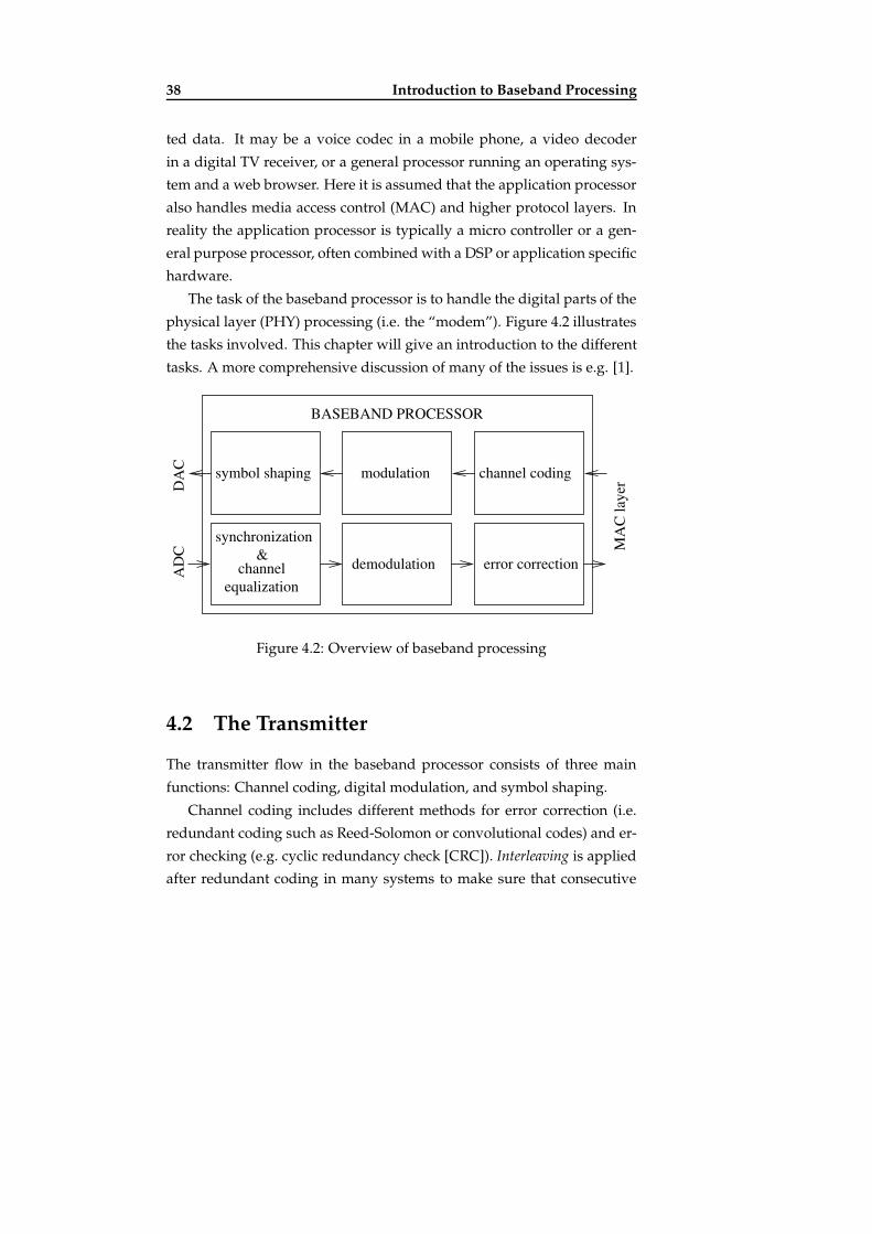
The task of the baseband processor is to handle the digital parts of thephysical layer (PHY) processing (i.e. the “modem”). Figure 4.2 illustratesthe tasks involved. This chapter will give an introduction to the differenttasks. A more comprehensive discussion of many of the issues is e.g. [1].
channel&
synchronization
equalization
symbol shaping modulation channel coding
error correction
BASEBAND PROCESSOR
MA
C la
yer
AD
CD
AC
demodulation
Figure 4.2: Overview of baseband processing
4.2 The Transmitter
The transmitter flow in the baseband processor consists of three mainfunctions: Channel coding, digital modulation, and symbol shaping.
Channel coding includes different methods for error correction (i.e.redundant coding such as Reed-Solomon or convolutional codes) and er-ror checking (e.g. cyclic redundancy check [CRC]). Interleaving is appliedafter redundant coding in many systems to make sure that consecutive

4.2 The Transmitter 39
I
Q
0000
0001
0011
0010 0110 1110 1010
0111 1111 1011
0101 1101 1001
0100 1100 1000
I
Q
16−QAMI
Q+1
+1
+1
−1
−1
−1
+3
+3
−3
−3
−1
+1BPSK
−1 +1
0 1
01 11
00 10
QPSK
Figure 4.3: Examples of signal constellations
bits in the bit stream are not transmitted consecutively in time (or on thesame frequency in the OFDM case). Thereby the robustness against bursterrors is improved. Scrambling is often used to turn the bit stream into apseudo-noise sequence without long runs of ones or zeros.
Digital modulation is the process of mapping a bit stream to a streamof symbols, each consisting of a number of complex samples. The first(and sometimes the only) step of the modulation is to map groups of bitsto complex values according to a specific signal constellation as shownin figure 4.3. In most cases, a second step called domain translation isused. In an Orthogonal Frequency Division Multiplexing (OFDM) sys-tem, an inverse fast Fourier transform (IFFT) is used for this step. In di-rect sequence spread spectrum (DSSS) modulation the complex value ismultiplied by a so called spreading sequence of ones and minus ones, seefurther sections 4.4 and 4.5.
The last step is symbol shaping which consist of transforming thesquare wave into a band-limited signal, typically using a finite impulseresponse (FIR) filter. This is necessary to make sure no part of the trans-

40 Introduction to Baseband Processing
mitted signal lies outside the permitted frequency band.The real and imaginary part of the complex valued signal, also known
as the in-phase (I) and quadrature-phase (Q) signals, are converted intoanalog signals and sent to the radio front-end. The I and Q signals aremixed with carrier signals with a 90 degrees phase difference and added.The result is a sinusoid signal at the carrier frequency with an amplitudecorresponding to the absolute value of the complex number and a phasecorresponding to the argument of the complex number. This signal isamplified, filtered, and transmitted through the antenna.
4.3 The Receiver
The receiver flow is essentially the opposite of the transmitter flow: Thebaseband processor receives the digitized I and Q signals and has to re-generate the transmitted bit stream.
Reception is significantly more challenging than transmission sincethe transmitted signal is affected by several kinds of distortions beforereaching the baseband processor.
Some challenges that must be handled are:
• Noise
• Multi-path channel fading
• Mobility
• Large dynamic range
• Frequency offset between transmitter and receiver
• Non-linearities and other distortion in RF and analog circuits
4.3.1 Dynamic Range
The strength of the received signal can vary dramatically depending onthe distance to the transmitter and depending on channel conditions. It
4.3 The Receiver 41
is not unusual to have to handle a dynamic range of 60-100 dB [2]. Sinceit is not practical to design systems with so large dynamic range, severallevels of automatic gain control (AGC) is normally used. The receivedenergy must continuously be measured and the gain of front-end compo-nents adjusted to normalize the received energy at the ADC. With a goodgain control algorithm fewer bits are needed in the ADC and basebandprocessor.
4.3.2 Synchronization
Synchronization can be divided into two steps. The first step is to detectan incoming signal or frame, this is known as energy detection. Functionssuch as AGC, frequency offset estimation, and antenna selection may alsobe carried out at this time. The next step is symbol synchronization whichaims to determine the exact timing of incoming symbols. These opera-tions are typically based on complex auto or cross correlations. In manysystem, each frame contains a known preamble or pilot sequence used forthis purpose.
4.3.3 Channel Estimation and Equalization
In essentially all radio systems the transmitted signal is subject to multi-path propagation, i.e. the received signal will contain multiple copiesof the tranmitted signal due to reflections of objects in the environment.The different signal paths will have different strength and timing and willadd constructively or destructively at different frequencies. The effects ofmulti-path propagation is known as fading. One such effect is overlapbetween consecutive symbols, so called inter-symbol interference (ISI).
The fading can be characterized by the impulse response of the chan-nel. One way of measuring the severity of the fading is the RMS delayspread which describes the root-mean-square distance in time betweenthe different signal paths.
If the symbol time is significantly longer than the delay spread (or inother words if the signal bandwidth is small enough), the fading can be

42 Introduction to Baseband Processing
considered constant over the signal spectrum, so called flat fading. Whenflat fading can not be assumed the receiver must compensate for the fad-ing by channel equalization.
In outdoor environments the difference between signal paths can bein the order of several micro seconds. As an example a delay spread of 1µs corresponds to a 300 m difference between the propagation paths. Un-der such conditions the minimum symbol time without advanced channelequalization would be approximately 10 µs (ten times the delay spread),corresponding to a symbol rate of 100k symbols/s.
In most cases correlation with known data is used to estimate thechannel and some kind of filtering is used for equalization.
4.3.4 Frequency and Timing Offset
If the oscillator frequencies in the transmitter and receiver are not exactlythe same this will cause a small rotation in the complex number planebetween each consecutive sample. In many systems, this error must beestimated and compensated. This is done either by modifying the oscil-lator frequency via some adaptive algorithm, or by rotating each sampleslightly relative to its predecessor.
One way of avoiding part of the problem is by using differential modula-tion where the information is represented by the phase difference betweento consecutive symbols instead of the absolute phase.
However, unless the oscillator frequency is controlled one may stillhave to compensate for timing offset, i.e. the difference between sampletime in ADC and DAC. For example samples may have to be inserted orremoved from the data stream at regular intervals.
4.3.5 Mobility
In a situation where the transmitter or receiver is not stationary the chan-nel conditions will change continously. This means that an estimated setof channel parameters will become obsolete after a certain period of time,known as the channel coherence time. In systems with high mobility, the

4.4 OFDM Modulation 43
channel coherence time may be in the order of one or a few symbol timesand the channel must therefore be continously tracked. This may con-sume a very significant part of the processing power in the receiver. Inthe WLAN applications discussed later in this thesis, the channel can beassumed to be stationary for the duration of a frame.
Mobility also causes Doppler shift which results in effects similar tothose caused by frequency offset.
4.3.6 Demodulation and Channel Decoding
Demodulation is the opposite operation of modulation. It involves anFFT in OFDM systems and correlation with the spreading sequence inDSSS systems. The last step of demodulation is demapping, i.e. findingthe closest point in the constellation diagram and converting the complexvalue into one or more bits.
Channel decoding consists of deinterleaving, error correction, descram-bling, and possibly error checking. Error correction (e.g. Viterbi or turbodecoding) tends to be very demanding functions.
4.4 OFDM Modulation
OFDM is a modulation method where the data is sent over a large num-ber of adjacent sub-carrier frequencies simultaneously. The symbols to betransmitted on each of the sub-carriers are collected in the frequency do-main and are all simultaneously transformed to a time domain signal us-ing an IFFT.
The idea is that each sub-carrier signal should have a very small band-width and hence only be subject to flat fading. Thereby a complex chan-nel equalizer can be avoided. Instead channel equalization only consistsof multiplying each sub-carrier with a complex valued constant in orderto scale and rotate the constellation point to its correct position. To fur-ther increase the robustness against ISI a cyclic prefix (CP) is often addedto each symbol after the IFFT. The CP acts as a guard interval: as long as

44 Introduction to Baseband Processing
the delay spread is shorter than the CP, the ISI is not a problem.OFDM presently seems to be gaining in popularity. It is used in e.g.
the IEEE 802.11a and IEEE 802.11g Wireless LAN standards, digital audioand video broadcasting (DAB/DVB), and the recent WiMax standard. It isbeing considered for several future standards including fourth generationmobile telephony. Figure 4.4 illustrates typical OFDM processing flows.
4.5 Spread Spectrum Modulation
The purpose of spread spectrum modulation is to spread the radio signalover a larger spectrum than necessary in order to make it less sensitive tointerference. Two basic types of spread spectrum modulation exists.
In frequency hopping spread spectrum, the transmitter regularly alter-nates between different carrier frequencies according to a predeterminedpattern.
In direct sequence spread spectrum (DSSS), each symbol is multipliedwith a pseudo-noise sequence of lengthN to createN so called chips. Thisoperation is known as spreading andN is called the spreading factor. Thechips are then transmitted at N times the symbol rate. In the receiver thechips are correlated with the spreading sequence to recover the symbol.This is known as despreading. DSSS is used in the IEEE 802.11b WLANstandard (a.k.a. WiFi).
A variant of DSSS is code division multiple access (CDMA) which isused in the third generation mobile telephony systems. CDMA uses thefact that if each user uses its own spreading sequence (or code), whichis orthogonal to all other used spreading codes, several users can trans-mit on the same frequency in the same time slot. After despreading, theinterference from other users will just look like white noise.
In DSSS and CDMA systems a structure known as a rake receiver isoften used for channel equalization. In the rake receiver, different sig-nal paths are despread separately (usually the 3-6 strongest paths are se-lected) and the contributions from the different paths are then added con-structively.

4.5 Spread Spectrum Modulation 45
filteringfiltering
detectionpacketAGC
offsetfrequency
estimation
offsetfrequency
compensation
removeCP
FFT
equalizationchannel
demapping
deinterleaving
correctionerror
descramble scramble
codingchannel
interleaving
mapping
pilotinsertion
IFFT
CPadd
shapingsymbol
symbolsync.
bit−basedprocessing
processingprocessingprocessingpreamble receive transmit
estimationchannel
processingcomplex−valued
Figure 4.4: OFDM processing flows

46 Introduction to Baseband Processing
In e.g. 3G systems which may have a large delay spread (several mi-croseconds) and high mobility (terminals may travel at up to 250 km/h),the rake processing is the single most computing intensive part of the re-ceiver. Figure 4.5 illustrates the DSSS/CDMA processing flows.
4.6 MIMO Systems
MIMO, which stands for multiple input multiple output, is a method usedto reach higher data rate with a given bandwidth and SNR by using mul-tiple antennas in both transmitter and receiver. MIMO has been widelydiscussed over the last few years and is proposed e.g. for the upcomingIEEE 802.11n WLAN standard.
MIMO will cause considerable processing challenges for future base-band processors, e.g. in the form of matrix inversion operations necessaryin the receiver [3].
4.7 Computational Complexity
The computing capacity needed in the baseband processor depends main-ly on the data rate and the mobility. The requirements increase superlin-early with the data rate. For many parts of the flow, the number of oper-ations per data bit is constant. Other parts, e.g. channel equalization, willrequire more processing per bit when the symbol rate increases.
Mobility mainly determines how often channel estimation must be re-peated. The processing requirements for channel estimation and track-ing will be approximately inversely proportional to the channel coherencetime or proportional to the velocity of the transmitter or receiver.
Data rate and mobility for some standards is illustrated in figure 4.6.One main motivation for using a programmable processor is that withenough flexibility and a certain level of computing capacity a range ofsystems with different types of modulation and different trade-offs be-tween data rate and mobility can be covered.

4.7 Computational Complexity 47
demapping
deinterleaving
correctionerror
descramble scramble
codingchannel
interleaving
mapping
filtering
detectionpacketAGC
filteringshapingsymbol
processingprocessingprocessingpreamble receive transmit
symbolsync.
bit−basedprocessing
estimationchannel
processingcomplex−valued
spreaddespread/rake
Figure 4.5: DSSS/CDMA processing flows

48 Introduction to Baseband Processing
Bluetooth
data rate
mob
ility
complexity(MIPS)
computing
IEEE 802.11a
IEEE 802.16(WiMax)IEEE 802.11b
WCDMA (3G)GSM
(MIMO)IEEE 802.11n
Figure 4.6: Data rate and mobility for different standards
The performance of conventional DSP processors is typically only suf-ficient to manage low-rate, low-mobility systems. Even for moderate datarates (more than a few hundred kbit/s) or mobility requirements (morethan walking speed), high-end processors using VLIW/SIMD technolo-gies and/or operating at several GHz will be required. These processorsare often too expensive and power consuming. The rest of this thesis dis-cusses how more cost- and power-efficient programmable solutions canbe obtained.
Bibliography
[1] John B. Anderson, Digital Transmission Engineering. IEEE Press, Pren-tice Hall, 1999. ISBN 0-7803-3457-4.
[2] Bosco Leung and Behzad Razavi, RF Microelectronics. Prentice Hall,Pearson Education, Inc., 2004. ISBN 0-13-861998-0.

4.7 Computational Complexity 49
[3] Haiyan Jiao, Anders Nilsson, Eric Tell, and Dake Liu, “MIPS cost es-timation for OFDM-VBLAST systems,” in paper submitted for review,2005.

50 Introduction to Baseband Processing

Chapter 5
Programmable BasebandProcessors
5.1 Introduction
This chapter will discuss what implications the properties of typical base-band applications have on the design of ASIPs for baseband processing.The focus is on terminals for mobile telephony and computer networking.The requirements are slightly different for unidirectional or broadcastingstandards such as DAB and DVB since the latter need more data memorybut have less requirements on latency.
5.2 Processing Requirements
Going back to figures 4.4 and 4.5 it is clear that the operations needed in abaseband processor can be divided into to two main classes: Calculationsbased on complex valued data and bit manipulation operations. This sec-tion will discuss the implementation of these two types of operations.
51

52 Programmable Baseband Processors
5.2.1 Convolution-Based Complex-Valued Processing
The data between the ADC/DAC and the mapping/demapping consistsof I/Q-pairs, which are treated as complex values. The functions to be car-ried out are modulation/demodulation, synchronization, channel equal-ization, etc. The FFT function is heavily used in OFDM systems. In DSSSsystems, modulation/demodulation is based on multiplication/correla-tion with a spreading sequence. Other common operations are correla-tion, filtering, etc. These are all very common DSP algorithms, most ofthem convolution based. Traditional DSP processors are able to carry outthese kinds of algorithms rather efficiently thanks to MAC units and op-timized memory and bus architectures.
The following areas where optimizations can be made have been iden-tified:
Complex-valued computations: Since almost all computations are basedon complex-valued numbers, it is beneficial to optimize the ISA forcomplex calculations. This includes using complex data paths anddata types, and instructions for operations such as conjugate, mul-tiply by i, multiplication/MAC with conjugate, and complex abso-lute value.
Instruction level acceleration: In addition to the above mentioned oper-ations on complex values, a few operations common in basebandprocessing were found to be suitable for instruction level accelera-tion. This includes finding the position of the maximum complexabsolute value in a vector, accumulation of square absolute values,FFT butterfly, and combination of the last layer of FFT butterflieswith frequency domain filtering. All of these are certainly opera-tions that are common in other applications too. In a processor thatshould handle the IEEE 802.11b standard it may also be suitableto accelerate the modified Walsh transform butterfly (essentially aradix-4 FFT butterfly without multiplications). However, becauseof the high symbol rate in IEEE 802.11b it may be more suitable touse function level acceleration for the modified Walsh transform.

5.2 Processing Requirements 53
Data width optimization: The requirements on data precision is gener-ally low in baseband processing. As discussed in section 3.5.6, sig-nificant reduction of hardware size and power consumption can beachieved by keeping down the data width. The BBP1 baseband pro-cessor, presented in chapter 7, uses 16 bit native data width (16 bitsfor real and 16 bits for imaginary part) and 12x12 bit precision formultiplications. This was proven to be sufficient by behavioral sim-ulations of IEEE 802.11a and b systems.
5.2.2 Bit-Based Processing
Many of the processing steps between the interface to the MAC-layer andthe mapping/demapping are operations which are based on manipula-tion of individual data bits (e.g. channel coding, scrambling, interleaving,and CRC checksum calculation). This tends to make them rather ineffi-cient for software implementation. On the other hand, many of these op-erations can be implemented in a very small hardware block. For exam-ple, both scrambling, convolutional coding, and CRC can be implementedas simple linear feedback shift registers with XOR-gates. This fact oftenmakes these operations suitable for function level acceleration. These op-erations are also rather similar between different standards, which makesit beneficial to build configurable accelerators.
The required computing cost is on the other hand not extremely high,implying that software implementation may be suitable in some caseswith low or moderate data rates.
5.2.3 Error Correction
Error correction (e.g. Reed-Solomon, Viterbi, and turbo decoders) is gen-erally very demanding. Instruction level acceleration has been suggested,e.g. Galois field operations for Reed-Solomon [1] and add-compare-selectinstructions for Viterbi [2]. However, even with such instructions theMIPS cost is still high and in most cases these operations should be ac-celerated on function level. Again, good possibility of reusing such accel-

54 Programmable Baseband Processors
erators in several standards makes function level acceleration even moreattractive.
5.3 Real-Time Requirements
Essentially all radio systems we are interested in are hard real time sys-tems. Transmitted samples must be sent to the ADC at exactly the rightclock cycle and incoming data must be taken care of.
In many cases the latency requirements are also very though. Oneexample is the latency requirement for acknowledging a received packetin a WLAN system. As mentioned earlier, broadcasting systems such asDAB/DVB where latency is not a big issue are not considered here.
Implications of this is for example that regular cache memories orbranch prediction cannot be used because of the unpredictability in ex-ecution time it introduces, and that interrupt latencies need to be keptshort.
During the course of this project it was found that neither of thesefactors were limiting. The required memory sizes are quite small sincethe latency requirements does not allow a lot of data to be buffered in thebaseband processor. For example, in the BBP1 processor the total amountof memory is 65 kbit for program and 100 kbit for data. The use of cachesis of no interest with such small memory sizes. Furthermore, since theprocessing flow is to a large extent known, only rather simple controlfeatures and interrupt handling are sufficient, which simplifies reachinglow interrupt latencies.
The challenge was rather to find an architecture that allowed efficientscheduling and communication between the DSP core and accelerators.Once sufficient computing power and low communication overhead wasreached remaining problems were minor.
It should be noted though that detailed scheduling is necessary to de-termine the real hardware requirements. Simply using the average MIPScost is not sufficient. This is due to e.g. dependencies within receiveddata. In many cases, heavy processing is required during the preamble
5.4 Memory Issues 55
of a frame in order to perform synchronization and channel estimation.These operations must be completed before processing of the data sym-bols can start.
5.4 Memory Issues
As mentioned above, the required amount of data memory tends to berather small in baseband processing. On the other hand the memory ac-cess rate tends to be quite high. This means a significant total memorybandwidth is required if a moderate clock frequency is to be used.
Example 1: IEEE 802.11a is an OFDM system using 64-point FFTs. OneFFT+channel equalization requires a total of 1152 memory access. Eachaccess reads or writes a complex value of 16+16 bits. The symbol time is4µs resulting in 1152 ∗ (16 + 16)/4 = 9212 bits accessed per microsecond.If the processor runs at 160 MHz this means an average of 9212/160 =
58 bits per clock cycle just for the FFT and channel equalization duringpayload processing. Memory access rates for various systems has beenfurther studied in [3].
Example 2: The BBP1 processor has a dual complex MAC unit. To keepthe MAC fully occupied, up to 4 complex values needs to be read and twowritten every clock cycle, resulting in a required memory bandwidth of(16 + 16) ∗ (4 + 2) = 192 bits per clock cycle for the MAC unit only. At thesame time incoming data from the ADC have to be buffered and memorymay also be accessed by accelerators. On the other hand, the total amountof data memory needed for 802.11a reception (including FFT coefficientsand housekeeping variables etc.) is only 18.7 kbit, or equivalent to 585samples.
The conclusion of these examples is that a typical programmable base-band processor will have multiple memory blocks of relatively small size.Thanks to the regular access patterns and well known scheduling in base-band processing, dual port memories with their extra area and powercost can typically be avoided. Though dual port memories may simplifydesign, solutions using standard memories with smaller power and area,

56 Programmable Baseband Processors
and without increased cycle cost can usually be found. The memory issueis further discussed in section 7.5.
Bibliography
[1] H. Michel Ji, “An optimized processor for fast Reed-Solomon encod-ing and decoding,” in Proceeding of the IEEE International Conferenceon Acoustics, Speech, and Signal Processing, pp. III–3097–III–3100, May2002.
[2] Jeong Hoo Lee, Weaon Heum Park, Jong Ha Moon, and Myung H.Sunwoo, “Efficient DSP architecture for Viterbi decoding with smalltrace back latency,” in Proceeding of the IEEE Asia-Pacific Conference onCircuits and Systems, pp. 129–132, Dec. 2004.
[3] Anders Nilsson, Eric Tell, and Dake Liu, “Design methodology formemory-efficient multi-standard baseband processors,” in Proceedingsof Asia-Pacific Communications Conference (APCC), 2005.

Chapter 6
Related Work
6.1 Introduction
Not many academic publications are available in the area of program-mable baseband processors. Most of the existing publications focus onsmall parts of the system or on high level issues and very few on newarchitectures.
For many of the commercial solutions it is difficult to obtain detailedinformation without a none-disclosure agreement. Nevertheless, this chap-ter briefly presents some other, mainly commercial, solutions.
6.2 Rice University - Imagine
Rajagopal et al. have published one of the few existing academic paperson programmable baseband processor architectures [1]. The architectureis a modification of a media processor architecture from Stanford called“Imagine” [2]. It has eight VLIW-based computational clusters organizedin a SIMD fashion. Each cluster has three adders and three multipliers.The memory subsystem is stream based and optimized for media appli-cations.
At 500 MHz it can run WCDMA multi-user-detection [3] (i.e. the pro-cess used in a base station for simultaneous channel estimation and rake
57

58 Related Work
reception for several users) for 32 users under low or medium mobility.
6.3 Morpho Technologies - M-rDSP
Morpho Technologies provides the M-rDSP architecture[4]. It is basedon an array of between 8 and 64 reconfigurable cells (RCs) controlled bya 32-bit RISC unit. Each RC contains an ALU, a MAC unit, and specialfunctional units for wireless applications. The configuration of all RCsand interconnects is specified in a “context”. A context memory that canstore up to 512 different contexts allows the function of the RC array to bechanged every clock cycle.
The MS1-16 IP core has 16 reconfigurable cells and WCDMA-specificblocks for sequence generation and interleaving. Running at 500 MHz itsupports WCDMA, GSM/GPRS, and IEEE 802.11a/b/g. The silicon areais claimed to be 65% less and estimated power consumption 50% less thanother fully programmable DSP solutions.
6.4 Sandbridge Technologies - Sandblaster
Sandbridge Technologies Inc. has a processor architecture called “Sand-blaster” [5]. The processor has a RISC based integer unit and a SIMD unit.The Sandblaster uses a form of multithreading. The core holds contextsfor up to 8 threads simultaneously. The treads take turns to issue instruc-tions in a round-robin fashion. Every clock cycle one of the treads can is-sue one instruction. When a thread only issues one instruction every eightclock cycles, data dependency problems due to the deep pipelines andmemory latency are avoided. The Sandblaster architecture is intended tohandle both media and baseband processing.
The SB9600 chip contains four Sandblaster processors and an ARMmicro controller. Each Sandblaster core has 64 kByte of data memorydivided into 8 memory banks and a 64 kByte instruction cache. Thereis also a 256 kByte level two cache for each core. The SB9600 supports2Mbit/s WCDMA, GPS/GPRS and IEEE 802.11b running at 600 MHz.

6.5 SystemOnIC - Hipersonic 59
Low-power circuit techniques and fine-grained clock gating is used toachieve a power consumption of less than 500 mW.
6.5 SystemOnIC - Hipersonic
SystemOnIC, now acquired by Philips, developed a programmable base-band processor called “Hipersonic 1” [6]. Hipersonic 1 is designed forthe OFDM standards IEEE 802.11a and HIPERLAN/2. It is based on aflexible DSP core called OnDSP. It has one general data path and 8 SIMDdata paths, each including a 40-bit ALU, a barrel shifter, and MAC unitwith a 40-bit accumulator. The data paths are connected to a 128-bit-widedata memory via an interconnect unit. The general data path, memory, in-terconnect unit, and SIMD data paths are controlled using VLIW instruc-tions. A dynamic code-width reduction technique called tagged VLIW [7]is used to reduce program size. A small instruction cache (loop cache) isalso used.
Transmit and receive filters, channel coding (convolutional encoding,scrambling, CRC and Viterbi), and DES (Data Encryption Standard) en-cryption/decryption is handled by a hardwired coprocessor. A DMA unithandles data transfers between the DSP core and the coprocessor.
A chip including the Hipersonic core and ADC/DAC has a transistorcount of 7.6 million. The chip has 32 kByte of program memory and 15kByte of data memory. Extensive clock gating is used and the maximumpower consumption is 300-800 mW running at 120 MHz in a 0.18 µmCMOS technology.
6.6 Other Solutions
A common solution for reaching some flexibility is to use a general pro-cessor or DSP together with ASIC blocks. Usually the ASIC block haslow flexibility and most parts are standard specific. The programmableprocessor will mostly execute the control flow and very little of the dataprocessing.

60 Related Work
FPGA based solutions are discussed occasionally. These are to expen-sive and power consuming for most applications. Reconfiguration time isalso a problem.
Another alternative is configurable architectures [8]. These typicallyconsist of a configurable fabric of computing elements which are con-trolled by a programmable processor. The advantage compared to FPGAsis that they can be reconfigured dynamically at run-time. However, thereconfiguration time is still typically in the order of micro seconds whichmakes it difficult to reuse computing units for more than one task in atransmitter or receiver flow. So far the power consumption also tends tobe high.
6.7 Discussion
The solution from Rice university is just a minor modification of a pro-cessor designed for media applications. The performance for bit orientedtasks, e.g. Viterbi decoding, is low. It seems more focused on base stationprocessing and area and power efficiency is expected to be low.
The Sandbridge and Hipersonic solutions are in principle based onwell known VLIW and SIMD solutions. The solution from Morpho tech-nologies seems more innovative. Unfortunately, no detailed informationabout e.g. the interconnect and memory organization has been found.
None of the presented solutions use natively complex data paths, al-though it may be possible to to execute a complex operation in one clockcycle by combining VLIW/SIMD execution units.
The Hipersonic processor has a SW-HW partitioning similar to the oneproposed in this thesis while the other architectures rely more on wideSIMD/VLIW data paths even for bit oriented processing. None of theseprojects have any focus on flexible and efficient integration of hardwareaccelerators.
It is difficult to make quantitative comparisons between architecturessince the function coverage varies. Nevertheless, it seems very likely thatthe BBP1 processor presented in chapters 7 and 8 is more area and power
6.7 Discussion 61
efficient than all of the architectures described in this chapter, with thepossible exception of the solution from Morpho technologies. However,the other architectures may have more flexibility outside the basebandprocessing domain. The more regular architectures may also simplifyfirmware design and design tools. Sandblaster is programmed in stan-dard C while Hipersonic uses “Systemonic-C” which is described as a“C++ based high level assembler”.
Bibliography
[1] Sridhar Rajagopal, Scott Rixner, and Joseph R. Cavallaro, “A pro-grammable baseband processor design for software defined radios,”in Proceedings of the 45th Midwest Symposium on Circuits and Systems,pp. 413–416, 2002.
[2] B. Khailany, W. J. Dally, U. J. Kapasi, P. Mattson, J. Namkoong, J. D.Owens, B. Towles, A. Chang, and S. Rixner, “Imagine: Media process-ing with streams,” IEEE Micro, no. 2, pp. 140–147, 2001.
[3] S. Rajagopal, S. Bhashyam, J. R. Cavallaro, and B. Aazhang, “Real-time algorithms and architectures for multiuser channel estimationand detection in wireless base-station receivers,” No. 3, pp. 468–479,2002.
[4] Morpho Technologies. http://www.morphotech.com/.
[5] John Glossner, Daniael Iancu, Jin Lu, Erdem Hokenek, and MayanMoudgill, “A software-defined communications baseband design,”IEEE Communications Magazine, no. 1, pp. 120–128, 2003.
[6] Johannes Kneip, Matthias Weiss, Wolfram Drwscher, Volker Aue, Jür-gen Strobel, Thoms Oberthür, Michael Bolle, and Gerhard Fettweis,“Single chip programmable baseband ASSP for 5 GHz wireless LANapplications,” IEICE Transactions on Electron., pp. 359–367, Feb. 2002.

62 Related Work
[7] Matthias Weiss and Gerhard Fettweis, “Dynamic codewidth reduc-tion for VLIW instruction set architectures in digital signal proces-sors,” in Proceedings of IWISP, 1996.
[8] Srikathyayani Srikanteswara, Ramesh Chembil Palat, Jeffrey H. Reed,and Peter Athanas, “An overview of configurable computing ma-chines for software radio handsets,” IEEE Communications Magazine,no. 7, pp. 134–141, 2003.

Part III
The BBP1 Architecture
63


Chapter 7
The BBP1 BasebandProcessor Architecture
7.1 Introduction
This chapter will describe the main contribution of the presented work;the baseband processor architecture. The main goals set up at the start ofthe project can be summarized as follows:
• Find an efficient instruction set for baseband processing.
• Find which functions in a baseband processor are suitable for hard-ware acceleration and especially if it is possible to build flexiblehardware accelerators that can be reused between standards andfunctions.
• Find an efficient baseband processor architecture focusing on
1. Low computing latency and predictable hard real-time perfor-mance.
2. Minimized memory size and memory access overhead.
Meeting these goals would contribute greatly in reaching the ultimategoal of finding power and area efficient architectures for programmablemulti-standard baseband processors.
65

66 The BBP1 Baseband Processor Architecture
The main achievements resulting from this project are:
1. The DSP core and its instruction set, including a novel type of vectorinstructions.
2. The overall architecture, using a configurable network to connectthe accelerators and memories to the processor.
3. HW-SW codesign for IEEE 802.11a/b. Mapping and scheduling ofthese standards on the architecture.
The first two points are intimately connected since the efficient execu-tion of vector instructions relies on the network design and especially thememory subsystem with a number of small data memories with decen-tralized address generation.
This chapter will give an overview of the architecture followed by amore detailed description of the novelties of the instruction set, the mem-ory subsystem and the integration of accelerator units in the basebandprocessor. Sections 7.2 - 7.6 refers primarily to the first implementationof the architecture which was a baseband processor focused on WLANapplications. Much of these details have previously been published [1, 2].Section 7.7 will describe some possible variations of the architecture aswell as some scalability issues.
Chapter 8 discusses the demonstrator chip which was manufacturedas well as the developed design tools (assembler and simulator) and firm-ware for IEEE 802.11a and IEEE 802.11b1.
Appendix A contains a summary of the algorithms used in the WLANapplications and a quantitative motivation of ISA design choices based onthe MIPS costs and timing requirements of the standards.
7.2 Architecture Overview
Figure 7.1 gives an overview of the architecture. The core of the processoris an application specific DSP processor with a simple ALSU (arithmetic-
1In the rest of this thesis the IEEE 802.11a and IEEE 802.11b standards will sometimes berefered to as just 11a and 11b

7.2 Architecture Overview 67
logic-shift unit) and a specialized complex-MAC unit. The DSP core isconnected to a number of memories and accelerators via a configurablenetwork.
256x16
IM
256x32
DM1DM3
256x32
Applicationprocessor
ALSU
RF
16 bit
16x16 bits
16 bit datapath
Con
trol
Reg
iste
rs
MAC
cADD16
CM
AR1
AR3
Port IF2048x32
cMUL12x12 cMUL12x12
cADD16
cADD32 cADD32
Network DM0
256x32
DM2
256x32
MACIF
AR0 (32+32 bits)
AR2
CRC
DAC ADC
Interleave
Walsh
Demap
packet.det.rotorFIR
ViterbiConv.enc./
Scramble
Figure 7.1: Overview of the BBP1 architecture
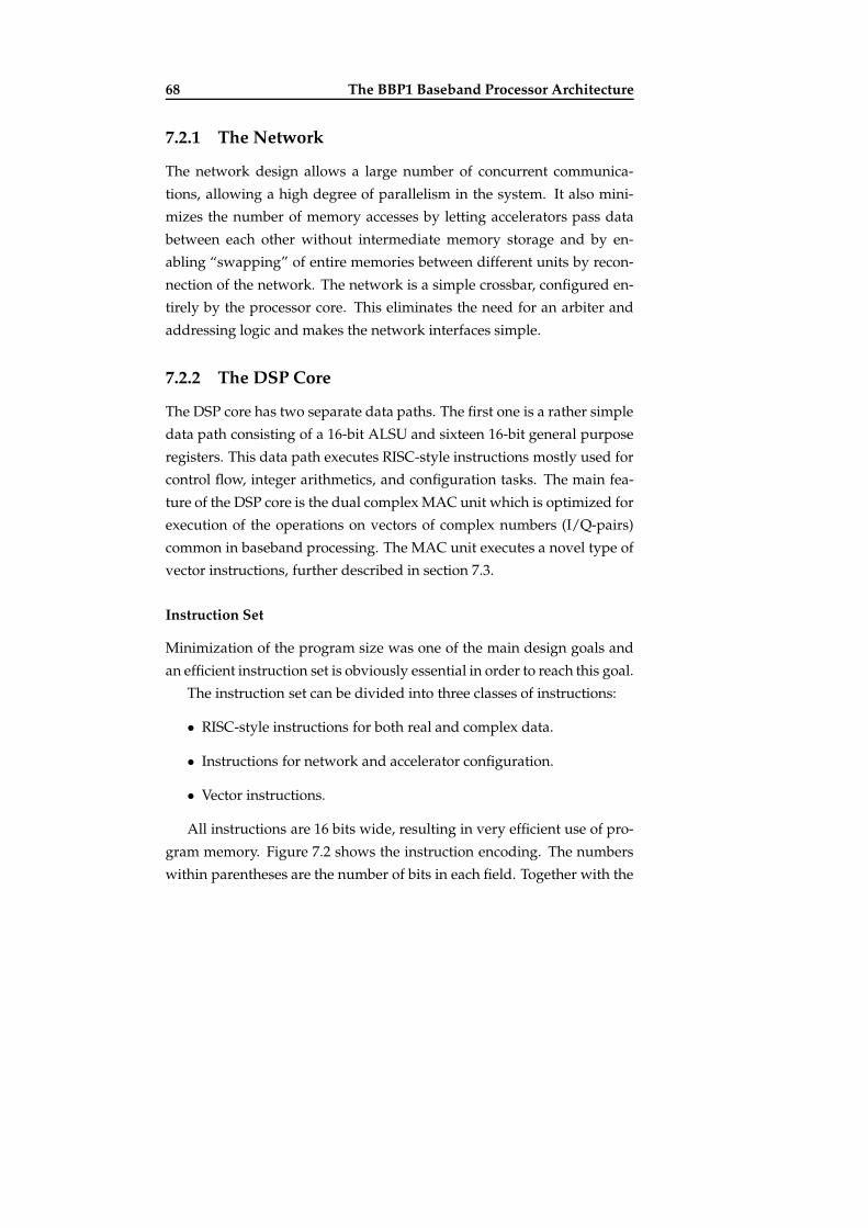
68 The BBP1 Baseband Processor Architecture
7.2.1 The Network
The network design allows a large number of concurrent communica-tions, allowing a high degree of parallelism in the system. It also mini-mizes the number of memory accesses by letting accelerators pass databetween each other without intermediate memory storage and by en-abling “swapping” of entire memories between different units by recon-nection of the network. The network is a simple crossbar, configured en-tirely by the processor core. This eliminates the need for an arbiter andaddressing logic and makes the network interfaces simple.
7.2.2 The DSP Core
The DSP core has two separate data paths. The first one is a rather simpledata path consisting of a 16-bit ALSU and sixteen 16-bit general purposeregisters. This data path executes RISC-style instructions mostly used forcontrol flow, integer arithmetics, and configuration tasks. The main fea-ture of the DSP core is the dual complex MAC unit which is optimized forexecution of the operations on vectors of complex numbers (I/Q-pairs)common in baseband processing. The MAC unit executes a novel type ofvector instructions, further described in section 7.3.
Instruction Set
Minimization of the program size was one of the main design goals andan efficient instruction set is obviously essential in order to reach this goal.
The instruction set can be divided into three classes of instructions:
• RISC-style instructions for both real and complex data.
• Instructions for network and accelerator configuration.
• Vector instructions.
All instructions are 16 bits wide, resulting in very efficient use of pro-gram memory. Figure 7.2 shows the instruction encoding. The numberswithin parentheses are the number of bits in each field. Together with the

7.2 Architecture Overview 69
vector instructions and acceleration of selected functions this results invery small program memory requirements (see table 8.1).
0 instr. (2−6) arguments (4−11)subtype (2−5)
10 instruction (4) ports (3) vector size (7)
Normal instruction (4 different formats):
Accelerator instruction:
Vector instruction:
11 control vector (10)accelerator ID(4)
Figure 7.2: Instruction encoding formats
Use of dedicated instructions for configuration of the network andaccelerators will reduce the overhead for such tasks compared to usingmemory mapped registers or similar for configuration. Considering theextent to which the architecture relies on efficient integration of acceler-ators and how a baseband application typically would make use of thepossibility of swapping memories between units, the small extra com-plexity of the control path due to these special instructions can certainlybe justified.
Much of the configuration can also be carried out via a control reg-ister file. The control register space is also used for e.g. data path andinterrupt configuration, and for communicating status information fromaccelerators and other hardware components.
Pipelining
All non-vector instructions use three pipeline stages (fetch, decode, andexecute), except instructions reading from the network which use two ex-ecution stages. Vector instructions have 5-8 pipeline stages.

70 The BBP1 Baseband Processor Architecture
PC
Control 0
Control 1
flagsinterrupts
Program Flow Control(jumps, interrupts,hardware loops etc.)
Control
Vector
check
instr.
instr. type
instr.
nop
Datapath
Control 4
PMInstruction
Decoder
count
Instruction
Figure 7.3: The control path
Control Path Features
An overview of the control path of the processor can be found in figure7.3. The control path complexity is similar to what can be found in sim-ple DSP processors or micro controllers but with the addition of the vec-tor instruction control unit which handles the multi cycle vector instruc-tions. The control path has been kept very simple to eliminate controloverhead which is typically quite substantial in enhanced processor typessuch as VLIW and superscalar processors. The vector instruction controlunit adds only little extra hardware. Much of the control path originatesfrom a previously developed extensible DSP processor [3].
Features of the control path include a zero overhead hardware loopinstruction and hardware PC and loop stacks, allowing fast interrupts,subroutine jumps, and nested hardware loops. Operand stopping is usedto reduce power consumption.
The processor uses fast interrupts, meaning that only PC and statusregisters are saved on interrupts. Data registers will have to be savedmanually. This simple approach was chosen because it allows very shortinterrupt latency (five clock cycles in the worst case) and small hardwarecost. It was found that most interrupt handling routines in the applica-

7.2 Architecture Overview 71
tions of interest are simple tasks such as reconfiguration of the networkor some of the accelerators, which does not require context switching.
The processor uses programmable interrupt vectors (i.e. the interruptaddress for each interrupt source is programmable) for up to 8 separateinterrupt sources. This includes two external interrupt pins, timers, inter-rupts from accelerators, and a special interrupt signaling the completionof a vector instruction. Accelerators may generate interrupts after com-pleting a task, after processing a certain number of samples or on eventssuch as packet detection (see section 7.6.7).
Pipeline conflict checks are not done by the hardware. This means thatundefined execution results may occur if illegal instruction sequences areused (e.g. executing an instruction using the MAC unit when a vectorinstruction is being executed). All such checks are instead done automat-ically by the instruction set simulator during software development.
Although some dependency checking was implemented in the previ-ous processor [3] it was not implemented in BBP1, mainly to save imple-mentation and verification time. Such features are typically not as im-portant in embedded processors since the applications are usually wellknown and extensively simulated before deployment.
Register forwarding features are are of little interest in BBP1 since (1)RISC instructions only have a single execution cycle, so the result is avail-able for the next instruction anyway and (2) for network accesses it wouldincrease the critical path as long as the network is not further pipelined.The only situation where it may be applicable is when a vector instructionis followed by a data move from accumulator to general register.
7.2.3 The MAC Unit
The MAC unit is the most substantial part of the DSP core. It is opti-mized for operations on vectors of complex numbers. Since such a sig-nificant fraction of the convolution/multiply-accumulate based opera-tions in baseband processing is complex valued it was found beneficialto optimize the MAC unit for such computations even at the expense of

72 The BBP1 Baseband Processor Architecture
slightly larger overhead for real-valued computations. Figure 7.4 depictsthe MAC unit.
The unit contains two complex 12x12 bit multipliers (i.e. eight realmultipliers), two 32-bit complex adders (for accumulation 8 guard bitsand 8 precision bits are added to the 16 native bits), and two 16-bit com-plex adders. It has four 32+32 bit accumulator registers. It can carry outfor example two complex multiply-accumulate operations or one radix-2FFT butterfly each clock cycle. It also supports scaling, rounding, andsaturation of the result.
7.3 Vector Instructions
The introduction of vector instructions is the single most important nov-elty in the design of the processor core. Through their introduction wereach a higher efficency, smaller program size, and increased parallelismduring execution of complex vectors operations, such as vector addition,scalar products, correlation, FIR-filtering, FFT, vector absolute maximumsearch, etc.
The vector instructions have the following properties:
• They operate on vectors of complex numbers. The vector size canbe any number between 1 and 128 and is given explicitly in the in-struction.
• The operand vectors are normally read from memory but may alsocome directly from an accelerator or external interface (see furthersection 7.4). The result is stored in memory or sent to an acceleratoror external interface, unless the result is scalar (i.e. the result of ascalar product or max search) in which case it is stored in one of thefour accumulator registers.
• Vector instructions require multiple clock cycles to complete, de-pending on the vector size. However other instructions not usingthe MAC unit may execute in parallel with the vector instruction.

7.3 Vector Instructions 73
+/−+ +/−+
trunc trunctrunc trunc
CMUL12 CMUL12
shift
conj.
neg.
shift
round
shift
conj.
neg.
round
shift
SAT SAT
conjugate conjugate
trunc
trunc
"0" "0"
16b 16b 16b 16b
12b 12b 12b
24b 24b
12b
"0" "0"
ara arc
ardarb
AR0 AR1 AR2 AR3
conj/swap conj/swap
sgn. ext. sgn. ext.
opa opb
opaopbfrom general register
from ports
I n p u t f r o m p o r t s
ara arb arc ardto ports or general registers
Figure 7.4: The MAC unit

74 The BBP1 Baseband Processor Architecture
only vector instruction: 53%
vector instruction + "free" instruction: 10%
instruction: 37%only non−vector
Figure 7.5: Fraction of the execution clock cycles spent on vector instruc-tions and other instructions
FFT.64 port1,port0 ; last layer of 64-point FFT
ADD R0,R1 ; “free” control flow instructions
MVR2CR R1,CR25
ACL dm0,read|0x00 ; setup addressing for...
ACL dm0,rstep|2 ; ...square abs max search
IDLE mac ; wait for FFT vector instruction to finish
SQRABSMAX.64 port2,AR0 ; find square absolute max value
Figure 7.6: Illustration of instruction parallelism. FFT.64 and SQRABS-MAX.64 are vector instructions
The fact that other instructions, such as integer arithmetics and ac-celerator and network configuration, can execute in parallel often allowspart of the cycle cost for control flow code to be hidden behind vectorinstructions. This is illustrated in figure 7.6. Note that although vectorinstructions and RISC instructions execute in parallel, they are not issuedin parallel. In other words, during the clock cycle the vector instructionis started, no other instruction can execute. The first RISC instruction isexecuted in the next clock cycle. This is illustrated in figure 7.7. It is thisfact that allows us to keep a very simple control path, instead of resortingto a VLIW or superscalar solution.
Statistics collected from the execution of the implemented firmwareshowed that approximately 20% of all non-vector instructions were hid-den and executed without any extra cycle cost. Figure 7.5 shows the frac-tion of the execution cycles spent executing vector instructions and non-vector instructions. Table 7.1 gives some examples of vector instructionsand their use.
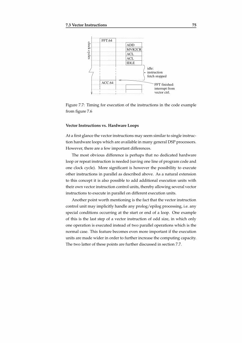
7.3 Vector Instructions 75
idle:instructionfetch stopped
clock cycles
ADDMVR2CRACLACLIDLE
FFT.64
ACC.64
interrupt fromvector ctrl.
FFT finished:
Figure 7.7: Timing for execution of the instructions in the code examplefrom figure 7.6
Vector Instructions vs. Hardware Loops
At a first glance the vector instructions may seem similar to single instruc-tion hardware loops which are available in many general DSP processors.However, there are a few important differences.
The most obvious difference is perhaps that no dedicated hardwareloop or repeat instruction is needed (saving one line of program code andone clock cycle). More significant is however the possibility to executeother instructions in parallel as described above. As a natural extensionto this concept it is also possible to add additional execution units withtheir own vector instruction control units, thereby allowing several vectorinstructions to execute in parallel on different execution units.
Another point worth mentioning is the fact that the vector instructioncontrol unit may implicitly handle any prolog/epilog processing, i.e. anyspecial conditions occurring at the start or end of a loop. One exampleof this is the last step of a vector instruction of odd size, in which onlyone operation is executed instead of two parallel operations which is thenormal case. This feature becomes even more important if the executionunits are made wider in order to further increase the computing capacity.The two latter of these points are further discussed in section 7.7.

76 The BBP1 Baseband Processor Architecture
Table 7.1: Examples of vector instructionsMAC Scalar product, correlation, FIR filteringVADD Vector additionVMUL Elementwise vector multiplication, multiply vector
by scalarFFT One layer of fast Fourier transform butterfliesFFT2 Includes frequency domain filtering in last layer of
and FFT, e.g. for OFDM channel equalizationSQRABS Vector elementwise square absolute valueSQRABSACC Sum of square absolute values, vector energySQRABSMAX Find value and position of maximum square abso-
lute value
7.4 The Accelerator Network
Most components are connected to the DSP core via the network. Thisincludes data memories, accelerators, and external interfaces (ADC, DACand MAC-layer interfaces). All components have essentially the sameinterfaces (although data width may vary) and look the same to the pro-cessor core.
The network behaves like a crossbar switch which is configured en-tirely by the core by way of dedicated instructions. This eliminates theneed for arbitration and addressing logic thereby reducing the complex-ity of the network and the accelerator interfaces while still allowing manyconcurrent communications. Since some units will never need to commu-nicate directly, the complexity of the network can be further reduced byapplying restrictions to what connections are possible.
Each network port consists of a pair of one read port and one writeport. A connection is set up by connecting one read port to one write port.The reading unit requests one word of data by asserting a ReadRequest sig-nal during one clock cycle and the transmitting unit uses a DataAvailablesignal to indicate that new data is available on the port. The requestingunit may have up to two outstanding read requests, but must then halt
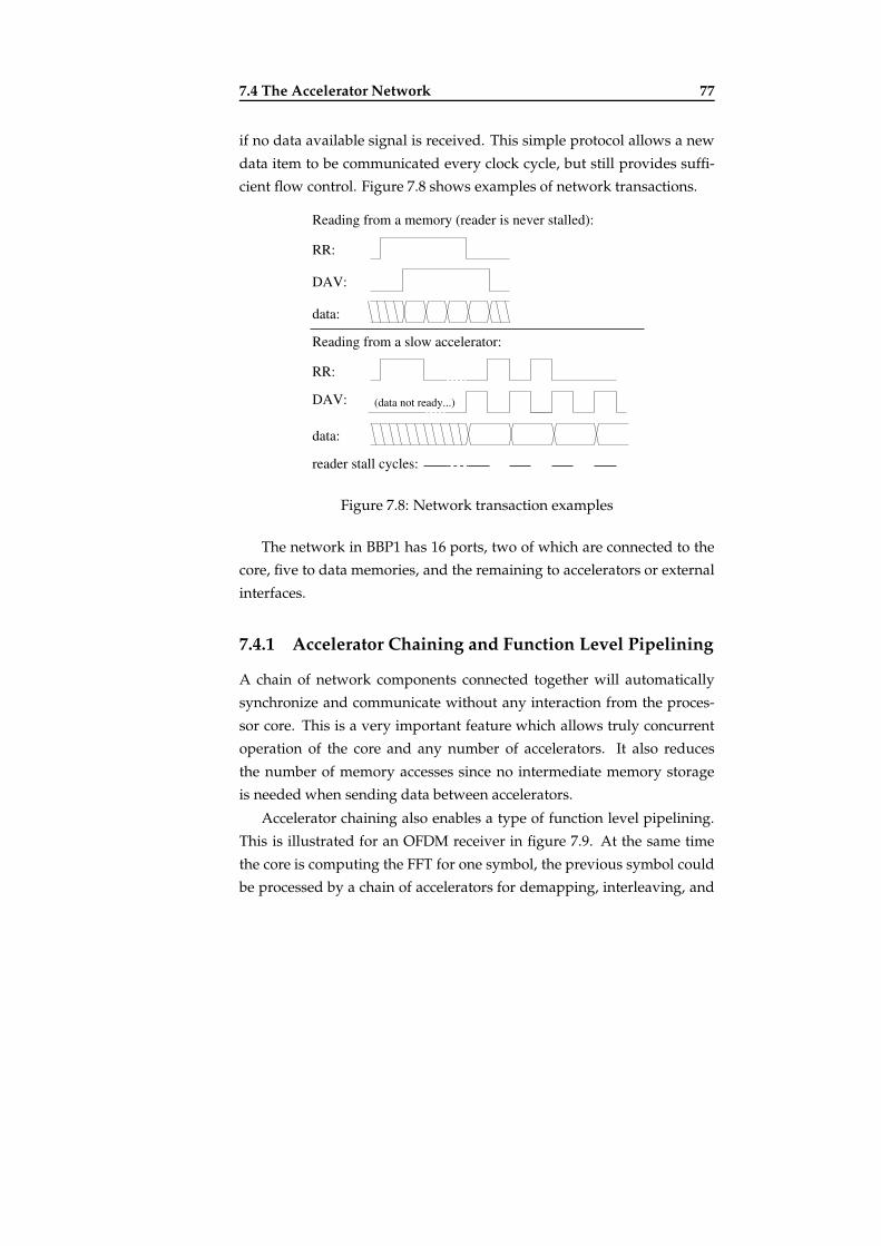
7.4 The Accelerator Network 77
if no data available signal is received. This simple protocol allows a newdata item to be communicated every clock cycle, but still provides suffi-cient flow control. Figure 7.8 shows examples of network transactions.
(data not ready...)
reader stall cycles:
DAV:
data:
RR:
data:
DAV:
RR:
Reading from a slow accelerator:
Reading from a memory (reader is never stalled):
Figure 7.8: Network transaction examples
The network in BBP1 has 16 ports, two of which are connected to thecore, five to data memories, and the remaining to accelerators or externalinterfaces.
7.4.1 Accelerator Chaining and Function Level Pipelining
A chain of network components connected together will automaticallysynchronize and communicate without any interaction from the proces-sor core. This is a very important feature which allows truly concurrentoperation of the core and any number of accelerators. It also reducesthe number of memory accesses since no intermediate memory storageis needed when sending data between accelerators.
Accelerator chaining also enables a type of function level pipelining.This is illustrated for an OFDM receiver in figure 7.9. At the same timethe core is computing the FFT for one symbol, the previous symbol couldbe processed by a chain of accelerators for demapping, interleaving, and

78 The BBP1 Baseband Processor Architecture
channel decoding, while the next symbol is received, decimated, and dero-tated by the front end accelerator (see 7.6) and stored in memory.
Synchronization between the pipeline steps can be achieved by inter-rupt signals from accelerators upon completion of tasks, by timers, or bya sample counter feature in the front-end accelerator.
n n+1 n+2Timeslots:
Symbol n+2Symbol n Symbol n+1
Symbol n+1Symbol n
Symbol n
Pipeline stage 1(front−end accelerator)
Pipeline stage 2
Pipeline stage 3(accelerator chain)
(DSP core) channelcompensation
compensation
bits to MAC−layer
samples from DAC,decimation,
FFT,
frequency offset
demapping,decoding,
Figure 7.9: Function level pipelining
7.5 Data Memory Architecture
As mentioned earlier, reducing the amount of memory and memory ac-cesses was a major goal in the design. Using a number of small data mem-ories gives enough memory bandwidth to keep the core and MAC fullyoccupied while simultaneously buffering incoming data from the radiofront-end interface and feeding accelerators or the MAC-layer interface.
Since the memories are so small and thereby fast, there is no need forcache memories. Thereby a major source of control overhead and unpre-dictability is eliminated. The network always gives a unit (core or accel-erator) exclusive access to a memory. This eliminates stall cycles due toaccess conflicts and gives a highly predictable architecture.
Another important feature of the architecture is the possibility of switch-ing memories between units. In other words, when e.g. the DSP core has

7.5 Data Memory Architecture 79
finished a computation on a block of data, the entire memory contain-ing the result can be “handed over” to another unit by reconfiguration ofthe network. This eliminates data moves between memories and almosteliminates the communications overhead in terms of core clock cycles forsending data between core and accelerators. The only remaining over-head is typically 1-2 clock cycles for reconfiguration of the network and1-4 clock cycles for configuration of the memory addressing.
7.5.1 Address Generation
Address generation is carried out by address generation logic in eachmemory block. This means that no addressing information have to besent over the network. It also eliminates the need for address generatorsin the accelerators.
In the simplest case, the address generation unit in a memory blockis initialized by setting a base address and an increment register. In mostcases the increment register value will be one, e.g. for fetching consecu-tive elements of a vector one at a time, or two if two vector elements arefetched in parallel, see below.
All memories in BBP1 also support modulo addressing for implemen-tation of circular buffers. The four complex data memories DM0-DM3also support bit-reversed addressing for FFTs.
To increase the memory bandwidth all memories except IM consists oftwo interleaved memory banks. Thus all odd addresses are in one bankand even addresses in the other, allowing consecutive addresses (vectorelements) to be accessed in parallel. The implementation of the interfacesfor these units are essentially two network ports with shared control logic(i.e. both data, ReadRequest, and DataAvailable signals are doubled, butthe control logic is not).
One argument against each memory having its own address genera-tor is that accelerators may use special addressing schemes and then itwould be more natural to have the address generation in the acceleratorinstead. Otherwise each memory block that could potentially commu-

80 The BBP1 Baseband Processor Architecture
nicate with the accelerator would need to support a special addressingmode. However, it turned out that in fact all accelerators in BBP1 onlyuses post-increment addressing with an increment of one, i.e. alwaysreading/writing consecutive vector elements one at a time. Therefore theused solution is more beneficial.
One operation that typically is associated with irregular addressing isinterleaving. However, since this is a bit level operation it is much moreefficient to implement the interleaving with an entirely specialized mem-ory structure, i.e. the interleaver accelerator will have its own memory,designed specifically for interleaving, and the input and output to thenetwork will still use linear addressing. Such a block has been describedearlier [4].
A similar case would be an accelerator for FFT which may be a goodidea for OFDM based standards using very large FFTs, e.g. DVB. In thatcase it is also believed that a better idea would be to have dedicated cus-tomized memory blocks in the FFT accelerator, thereby eliminating theneed for FFT addressing for other memories. One possible design of anaccelerator for FFT, DCT, and Walsh transform (used at the higher datarates in 11b) has also been described [5].
One final example, which is of interest especially in CDMA systems,is addressing in a programmable solution for rake receivers. This wasdiscussed in [6].
Another solution is to use special address generator components con-nected to the network [7]. This is however not suitable in the presentedarchitecture due to increased latency, increased number of required net-work ports and increased network traffic among other things.
7.6 Function Level Acceleration for BBP1
This section will briefly describe the hardware accelerators used in BBP1.Acceleration decisions are based on MIPS costs (see appendix A) and es-timated hardware cost for each function in the IEEE 802.11a and b stan-dards.

7.6 Function Level Acceleration for BBP1 81
7.6.1 Channel Coding
IEEE 802.11a uses a convolutional encoder for channel coding and theViterbi algorithm for decoding. Puncturing is used to achieve differentcode rates. Both these functions are good candidates for acceleration, asstated in chapter 5.2.3. Since convolutional encoding and Viterbi decod-ing never run simultaneously the two functions are built into the sameaccelerator unit in order to save network ports and configuration logic.
7.6.2 Scrambling
To cover 11a and 11b scrambling and descrambling, three different modesare needed (since for 11a scrambling and descrambling are identical). Thethree different functions are very similar. A multi-mode scrambler caneasily be designed and uses very little hardware. Figure 7.10 shows thekernel logic of the scrambler.
xor x x x x1 2 3 4 x x x5 6 7
xor
mode
in
out
Figure 7.10: Combined IEEE 802.11a/b scrambler/descrambler
7.6.3 Interleaving
IEEE 802.11a uses a block interleaver. The block size is equal to one OFDMsymbol, i.e. between 48 and 288 bits depending on the data rate. Themulti-mode block interleaver described in [4] is used.

82 The BBP1 Baseband Processor Architecture
7.6.4 Demapping
Demapping is rather cycle consuming for large constellations such as 16-QAM and 64-QAM and acceleration is needed to reach enough through-put at the highest data rates for 11a. The demapper is a simple unit basedon four small adders.
7.6.5 Walsh Transform
A modified Walsh transform plus absolute maximum value search are thekernel operations of the CCK demodulation used in 11b. Acceleration ofthese steps decreased the required clock frequency for 11b reception at thehighest data rate by approximately 60 MHz. The hardware in the imple-mented accelerator contains 15 adders and and two multipliers makingthis the second largest accelerator after the Viterbi decoder.
7.6.6 CRC
CRC check sums are used for the 11b header and for the MAC frames (theMAC layer is the same for both standards). The cycle cost for software im-plementation would not be very high if only the 11b PHY checksum wasimplemented, but it does require a substantial amount of data memoryfor look-up table storage. The core of the CRC hardware is similar to thescrambler and consists of a feedback shift register and three XOR-gates.
7.6.7 Front-End Accelerator
The front-end accelerator contains the interfaces to ADC and DAC, a con-figurable FIR filter that can be used for symbol shaping or decimation, arotor (essentially an NCO and a complex multiplier) used for frequencyoffset compensation, and a packet detector based on auto correlation usedto wake the processor from sleep mode when an incoming packet is de-tected. These functions are used by many standards, runs much of thetime, and especially the filtering can be rather demanding.

7.7 Design Variations and Scalability Issues 83
7.7 Design Variations and Scalability Issues
7.7.1 Scalability - Increasing Computing Capacity
As mentioned in section 7.3, a natural extension of the vector instructionconcept would be to add more execution units with their own vector ex-ecution control. It would then be possible to execute multiple vector in-structions in parallel. The cost of this, apart from the extra execution unitsthemselves, would be the additional vector execution controllers and net-work ports. The cost of the vector execution control unit is very low andincreasing the network size is also not believed to be a problem in a prac-tical case, see section 7.7.3.
Another way of increasing computing capacity would be to increasethe width of the execution units, e.g. using a 4-way complex MAC unit in-stead of a double complex MAC. The two main complications this wouldintroduce is: (1) Increased memory bandwidth requirements to keep theunit fully occupied and (2) more complex prolog/epilog processing.
The first of these problems could be handled either by increasing thenumber of memory blocks, which would imply that the number of net-work ports would also be increased, or by making the memories wider.The latter solution seems more attractive, since it does not increase thelogical depth of the network and gives lower control complexity. Theslightly reduced flexibility with that solution is not believed to be an is-sue since vector elements are most often accessed sequentially.
The more complicated prolog/epilog conditions would lead to a slight-ly more complex vector execution control unit. Note however that thiscomplexity otherwise would have to be handled explicitly in the programby extra assembly instructions (as in a VLIW or SIMD processor) and/orconditional execution.
A possible configuration for future implementations of this architec-ture was presented in [6]. Here the MAC unit has been extended to a4-way unit and a 4-way complex ALU unit primarily optimized for de-spread and rake processing has been added. This configuration will sup-port most current OFDM and CDMA standards.

84 The BBP1 Baseband Processor Architecture
7.7.2 Simultaneous Multi-Standard Processing
One issue that was not addressed in BBP1 is the possibility of handlingstandards using full duplex or even running multiple standards simulta-neously. In a practical case it is not obvious that one actually will wantto run multiple standards simultaneously on the same processor, mainlydue to the scheduling and certification issues mentioned below. A multi-processor solution in which all simultaneously active baseband applica-tions run on separate processors would simplify things in both these as-pects. Nevertheless, the following issues have been identified and maybe considered in future work:
Fast Context Switching
As mentioned in section 7.2.2, the need for supporting context switch-ing on interrupts was not found in the applications for which BBP1 wasdesigned. However, in order to process several separate flows simultane-ously, fast context switching on interrupts would be helpful. One possi-ble solution is something similar to what is used for fast interrupts in theARM architecture [8], i.e. to duplicate some or all of the general registersand swap to a new set of registers in a single clock cycle on interrupts.
Multiple Front-End Interfaces
The implemented radio front-end interface allows simultaneous receptionand transmission and can therefore in principle handle the full duplexcase. It is also possible to add several front-end interface blocks of thesame type (or any other kind of interface for that matter) in order to han-dle simultaneous reception and transmission of multiple streams. In thatcase, more memory blocks would probably also be added for buffering inthe different streams.

7.7 Design Variations and Scalability Issues 85
Scheduling Issues
One very important issue that has not been thoroughly investigated isscheduling. In the implemented firmware each standard has been indi-vidually statically scheduled by hand and the feasibility of the schedulehas been proven in simulation. Scheduling of multiple simultaneouslyrunning standards is much more complex and dynamic scheduling maybe necessary. Approaches to scheduling and the need for scheduling toolswill be further investigated.
Certification
One issue that has come up in the context of simultaneous multi standardprocessing is that of certification. Any radio device must go through a cer-tification process to ensure that it will behave correctly in the system andnot interfere illegally with other devices. This is typically a rather timeconsuming and costly process. A multi-standard device must go througha certification process for each of the supported standards. One risk isthat if the firmware of different standards are intertwined and runningsimultaneously on the same processor, a modification of the firmware forone standard would make it necessary to recertify the device for all im-plemented standards. The cost of this process may be prohibitively high.
7.7.3 The Network
In the implemented BBP1 demonstrator chip (see section 8.4) the networkhas 16 ports. This network constitutes approximately 10% of the logicarea and has no critical signal paths. However, since the size of a fullcrossbar grows as the square of the number of ports, and the logic depthgrows as the logarithm of the number of ports, a limit on the number ofports will eventually be reached with the current network architecture.
In practical cases this is not believed to be a problem since the numberof ports will not be so much larger.
As previously discussed, the network complexity can be reduced byrestricting the crossbar. One solution of interest would be to divide the

86 The BBP1 Baseband Processor Architecture
network into two separate networks: One handling complex valued dataand one handling bit oriented data. The mapper/demapper acceleratorand the core could act as bridges between the two networks.
Finally it should be mentioned that the next generation processors inthis project will use fewer rather than more network ports. For examplethe possibility of building a general bit manipulation processor to replaceboth CRC, scrambling, channel encoding, and interleaving acceleratorswill be investigated.
Bibliography
[1] Eric Tell, Anders Nilsson, and Dake Liu, “A programmable DSP corefor baseband processing,” in Proceedings of IEEE Northeast Workshop onCircuits and Systems (NEWCAS), June 2005.
[2] Eric Tell, Anders Nilsson, and Dake Liu, “A low area and low powerprogrammable baseband processor architecture,” in Proceedings of the5th International Workshop on System-on-Chip for Real-Time Applications(IWSOC), July 2005.
[3] Eric Tell, Mikael Olausson, and Dake Liu, “A general DSP processor atthe cost of 23k gates and 1/2 a man-year design time,” in Proceedings ofIEEE International Conference on Acoustics, Signal, and Speech Processing(ICASSP), pp. 657–660, Apr. 2003.
[4] Eric Tell and Dake Liu, “A hardware architecture for a multi modeblock interleaver,” in Proceedings of the International Conference on Cir-cuits and Systems for Communications (ICCSC), June 2004.
[5] Eric Tell, Olle Seger, and Dake Liu, “A converged hardware solutionfor FFT, DCT and Walsh transform,” in Proceedings of the InternationalSymposium on Signal Processing and its Applications (ISSPA), pp. 609–612, July 2003.

7.7 Design Variations and Scalability Issues 87
[6] Anders Nilsson, Eric Tell, and Dake Liu, “A programmable SIMD-based multi-standard rake-receiver architecture,” in Proceedings of EU-SIPCO, Sept. 2005.
[7] H. Zhang, V. Prabhu, V. George, M. Wan, M. Benes, A. Abnous, andJ. M. Rabaey, “A 1-V heterogeneous reconfigurable DSP IC for wire-less baseband digital signal processing,” IEEE Journal of Solid State cir-cuits, vol. 35, pp. 1697–1704, Nov. 2000.
[8] David Seal, ed., ARM Architecture Reference Manual, 2nd ed. Addison-Wesley, 2000. ISBN 1-201-73719-1.

88 The BBP1 Baseband Processor Architecture
Chapter 8
Implementation
8.1 Introduction
To prove the feasibility of the presented architecture, the programmableWLAN processor described in chapter 7 has been implemented togetherwith design tools and firmware for IEEE 802.11a and IEEE 802.11b. Thischapter will give a brief overview of these various parts.
8.2 Design Tools
An assembler and an instruction set simulator, as described in section 3.3,were developed as soon as the first draft of the instruction set was com-pleted. These tools have later been updated according to the design itera-tions of the ISA as well as to add various features to increase their usabil-ity for RTL verification, firmware debugging, and benchmarking/profil-ing.
8.2.1 The Assembler
The assembler was implemented in C++ using the Flex lexical analyzergenerator [1], and Bison compiler generator [2]. It is based on a genericassembler implemented by Dr. Daniel Wiklund.
89

90 Implementation
8.2.2 The Instruction Set Simulator
The bit-true and cycle-true instruction set simulator was implemented inC++. The simulator features include:
• Standard debugging features for observability and controllability,breakpoints, etc.
• Data dependency checking (read-write, write-read, and write-writedependencies) and structural pipeline hazard checking. No suchchecks are performed in the hardware, as mentioned section in 7.2.2.
• Tracking of undefined data values.
• Possibility to load/save memory contents and input/output data invarious file formats to simplify exchange of data with other appli-cations, e.g. Matlab and RTL simulators.
• Possibility to run script files and use batch mode execution.
Organization of the Simulator
The organization of the simulator is illustrated in figure 8.1.The bottom layer consists of completely hardware independent classes
for bit true arithmetic operations on various data widths and trackingof undefined values. There are also classes for support of scheduling,dependency checking, and logging as well as base classes for definingoperations and instructions.
The middle layer consists of one class that stores the complete stateof all hardware except for accelerators and classes for describing all op-erations that instructions can perform on the hardware. Each instructionis described by a class that defines which operations it performs in eachpipeline stage. There are also classes describing different types of acceler-ators. Which accelerators should be instantiated and which network portthey are connected to can be defined at runtime.
The next layer is a simulator class with methods for controlling thehardware, execution of instructions, breakpoints, etc. Finally, a user in-

8.2 Design Tools 91
Hardwareindependentclasses
(hardware state)processor
simulator
arithmeticoperations scheduling base class for
operations
base class forinstructions
dependencychecking logging
Hardwaredescription
Simulatorinterface
userinterface
accelerators instructions
operations
Figure 8.1: Organization of the instruction set simulator
terface layer is implemented to let the user interact with the system viathe simulator class. The currently used implementation has a simple textbased user interface, but a GUI is under development.
The simulator was designed to allow easy plug-in of accelerators andto be simple to reuse for future architectures.
Simulator Execution Flow
Figure 8.2 depicts the flow used in the simulator to achieve cycle-true ex-ecution. When an execution command is issued by the user the simulatorwill fetch the next instruction from program memory at the address givenby the program counter (PC). The resource usage table of the instructionis first checked against already scheduled instructions. If any resource us-age conflict is found an error message is printed and execution is stopped.
Otherwise data dependency checking is done. If a possible data de-pendency error is found, a warning is displayed (the most common case

92 Implementation
clear stall flag
save accelerator results
execute accelerators
data dependency check
fetch instruction at PC
schedule operations fornew instruction
from user’execute’ command
execute scheduled operations
single step execution?
break point?
end of program?
set stall flag
user inputhalt, wait for
update PC
scheduling conflict? error message
save operation execution results
stall flag?
N
Y
N
Y
Y
Y
Y
Y
N
N
N
N
stall?
Figure 8.2: Simulator execution flow chart

8.3 Firmware 93
is that the instruction tries to use a result of a previous calculation whichis not yet completed). Next, all the sub-operations of the instruction isscheduled into their respective time slot (pipeline stage).
Each of the accelerators reads any input data and executes one clockcycle. The resulting output is not yet made available to other units, sincethey may still need data from the previous clock cycle. This way synchro-nization is kept.
Next all operations scheduled for the current clock cycle (belongingto one or more previous instructions) are executed. If any operation cannot execute due to network delays a stall flag is set and no result fromany operation will be saved. Instead all instructions will be delayed oneclock cycle and operations that was executed the current clock cycle willbe executed again during the next clock cycle.
If the processor was not stalled, the results of instruction execution arestored and PC is updated. The next PC value is is a function of interruptconditions, control flow instructions, hardware loops, and the status ofthe idle flag. Delayed jumps are implemented by scheduling a PC-updateoperation in a later clock cycle. The idle flag is set by the IDLE instructionand cleared when an interrupt occurs.
After saving all results produced by instructions, the outputs from ac-celerators are also saved (regardless of the stall flag). Execution is nowstopped if a break point or the end of the program is reached. Otherwiseexecution continues. If either of the stall or idle flags are set, no new in-struction is fetched during the next clock cycle.
8.3 Firmware
11a and 11b transmitters and receivers have been scheduled onto the de-scribed architecture and firmware has been implemented. The perfor-mance of the processor was evaluated in terms of the minimum clockfrequency necessary to meet all latency and throughput requirements atthe highest data rate in each standard (54 Mbit/s in 11a and 11 Mbit/s in11b). Table 8.1, shows the required frequencies and the program and data

94 Implementation
Table 8.1: Firmware implementation resultsTask Required freq. Program size Data memory
11a Tx 155 MHz 1020 bytes 3456 bytes11a Rx 160 MHz 1658 bytes 2340 bytes11b Tx 120 MHz 476 bytes 484 bytes11b Rx 110 MHz 1090 bytes 304 bytes
memory usage for each module.
The frequency limit for the 11b receiver is imposed by the throughputrequirements at the highest data rate while the 11a receiver has through-put requirements and latency requirements for minimum size packetsthat are approximately equally restricting. For both transmitters through-put requirements are the limiting factors.
The required program and data memory sizes are small, proving theefficency of the instruction set and the memory architecture. A combined11a and 11b firmware would require approximately half of the availableprogram and data memory on the demonstrator chip. The requirementsare lower than the sum of the figures in the table since a lot of the datamemory and some subroutines are reused between modules.
A detailed description of the scheduling and hardware mapping isprovided in appendix B. Since this is the first firmware version it is be-lieved that further optimizations of the code should be possible. It is alsopossible to make other trade-offs between cycle cost and program size.
8.4 Prototype Chip
The design was implemented in VHDL using the HDL Designer tool fromMentor graphics. Mentor Graphics’ ModelSim was used for RTL simula-tion, verification, and post synthesis net list simulation . Output from theinstruction set simulator was used as golden results.
Synthesis and backend flow was carried out using Synopsis backendtools. An Artisan standard cell library and memory generator was used.

8.4 Prototype Chip 95
The chip was manufactured in a 0.18 µm CMOS process from CharteredSemiconductor Manufacturing (CSM).
Power consumption is quoted at 160 MHz since that is the clock fre-quency that would be used for IEEE 802.11a or IEEE 802.11g processing.The quoted idle power is measured after execution of the IDLE instruc-tion, meaning that instruction fetching is stopped but all clocks are stillrunning at full speed.
Figure 8.3 shows a photo of the manufactured chip. All white boxesare memories. PM is the program memory and the remaining boxes aredata memories. Table 8.2 summarizes the chip features.
The chip does not include the Viterbi decoder. It was skipped in orderto meet the tapeout deadline. Hardware implementation of the Viterbialgorithm is a well explored area [3]. The silicon area of a Viterbi decoderfor IEEE 802.11a is estimated to approximately 1 mm2.
Table 8.3 shows the approximate area used by different parts of theprocessor. The estimations for individual logic blocks may be inexactsince it is based only on the fraction of the logic cell area (and not the rout-ing area) occupied by each block. The network in particular is expectedto use a larger fraction of the logic area because of the large amount ofinterconnects in that block.
Table 8.2: Chip feature summaryFeature ValueTechnology 0.18 µm CMOSChip area 5 mm2
Memory area 1.0 mm2
Logic area 1.9 mm2
Max frequency 240 MHzPackage 144 pin fpBGAPower consumption @160 MHz:Idle 44 mWPeak for 11a Reception 126 mW

96 Implementation
Figure 8.3: Die photo
Table 8.3: Chip area usageComponent Area Fraction of total areaControl path 0.18 mm2 6.1%MAC unit 0.46 mm2 15.8%Core data path except MAC 0.20 mm2 7.0%Memory addressing and control 0.22 mm2 7.7%Network 0.17 mm2 5.9%Accelerators 0.66 mm2 22.9%Logic total 1.89 mm2 65.4%Program memory 0.30 mm2 10.4%Data memories 0.70 mm2 24.2%Memory total 1.00 mm2 34.6%
8.5 Test Board and Measurement Setup 97
8.5 Test Board and Measurement Setup
A printed circuit board for test purposes was built. In addition to theBBP1 chip the board has an Atmel AVR microcontroller that is used forbooting and controlling the BBP1 via a serial cable from a PC. The BBP1can be clocked by an oscillator on the board, by an external clock, or bya slow clock generated by the microcontroller. For measurements, theboard is connected to a Tektronix TLA721 pattern generator and logic an-alyzer system.
The chip was tested with the same test suits that were used for RTLverification and with the implemented 11a and 11b transmitter and re-ceiver firmware. Receivers were tested with ADC data generated by be-havioral models and with recorded air data. The chip functions correctlyup to a clock frequency of approximately 240 MHz.
For power measurements, a special program was designed that con-tinuously computes 64-point FFTs and simultaneously operates most ac-celerators as well as ADC and MAC interfaces. This is believed to corre-spond to the peak power conditions during 11a processing.
Bibliography
[1] Free Software Foundation, GNU Flex 2.5 – Reference manual.http://www.gnu.org/software/flex/manual/, 2005.
[2] Free Software Foundation, GNU Bison 2.0 – Reference manual.http://www.gnu.org/software/bison/manual/, 2005.
[3] S. Bitterlich and H. Meyr, “Efficient scalable architectures for Viterbidecoders,” in Proceedings of the International Conference on Applications-Specific Array Processors, pp. 89–100, Oct. 1993.

98 Implementation

Part IV
Conclusions and FutureWork
99


Chapter 9
Conclusions
This chapter summarizes some of the most important conclusions and re-sults from the presented work. This includes general conclusions regard-ing programmable baseband processing, a unique programmable base-band processor architecture, and demonstration of the architecture in amanufactured demonstrator chip running application firmware at fullspeed.
9.1 Issues in Design of Programmable Baseband
Processors
Design of programmable baseband processors has been discussed. Start-ing from general knowledge in design of application specific processors,the specific properties and requirements of baseband processing applica-tions have been studied. The focus has been on low-cost and low-powerarchitectures useful in handheld wireless terminals.
Some general conclusions regarding design of programmable base-band processors have been drawn:
Complex-valued computations: A large part of the computations in base-band processing is convolution-based operations on complex data.Convolution-based operations can in general be implemented ef-ficiently in programmable processors (i.e. general DSP processors).
101

102 Conclusions
By introducing instructions and data paths for complex calculations,complex convolution-based functions can also be implemented effi-ciently.
Function level acceleration: Making the right choice of accelerators is im-portant to reach a power- and area-efficient solution. Bit manipula-tion operations such as scrambling, CRC, and channel coding areusually inefficient in software but have very small hardware imple-mentations. These operations are therefore often good candidatesfor acceleration although the MIPS may not be very high. Viterbiand Turbo decoding should be accelerated in most cases. Theseoperations occur with small variations in many standards, makingconfigurable accelerators a good choice. It is also a good idea toaccelerate some operations close to the ADC/DAC interface, suchas symbol shaping, decimation, and frequency offset compensation.Such functions are used in most standards, are running a large frac-tion of the time, and are rather computing intensive at high samplerates.
Since the data blocks in baseband processing are usually small, it isimportant to integrate the accelerators in the architecture in a waythat provides low communication and control overhead.
Memory issues: The amount of memory required in a baseband proces-sor is generally low but the required memory bandwidth is oftenrelatively high. High memory bandwidth can be reached either byusing wider memories, several memory banks, or dual port memo-ries. The memory access patterns in baseband processing are knownin advance and often very regular. Therefore dual port memories,being the most flexible but also the most costly solution, usually canand should be avoided.

9.2 An Architecture for Efficient Baseband Processing 103
9.2 An Architecture for Efficient Baseband Pro-
cessing
A programmable baseband architecture has been presented. The architec-ture enables a good tradeoff between flexibility and performance and hasproven to result in area- and power-efficient implementations of multi-standard programmable baseband processors.
Important novel features are:
• Vector instructions in which the vector size is given explicitly inthe instruction. This saves program memory and allows instructionlevel parallelism without significant increase of control path com-plexity.
• An instruction set optimized for baseband processing, includingvector instructions for operations on complex data.
• A scheme for interconnection of accelerators, memories, and pe-ripherals to the programmable core via a configurable network. Thisscheme allows a high degree of parallelism and low overhead forcommunication and accelerator configuration. This is achieved byusing a simple network which is statically scheduled and config-ured by the programmable core. The network is closely coupled tothe instruction set architecture e.g. in terms of dedicated instruc-tions for network and accelerator configuration.
9.3 Implementation Results
A demonstrator chip was manufactured to prove the architecture. Theimplemented processor was optimized for the WLAN standards IEEE802.11a, b, and g. It includes accelerators for front-end operations, demap-ping, scrambling, CRC, interleaving, channel coding, and modified Walshtransform.
11a and 11b baseband PHY was mapped and scheduled on the archi-tecture. Firmware was developed and tested on the manufactured chip.

104 Conclusions
The required silicon area is similar to what can be reached in a fixed func-tion 11a/b baseband solution.
Measurements proved that the chip can operate at significantly higherspeeds than those needed for the mentioned standards. Power consump-tion was also found to be competitive to fixed function solutions.
The ultimate conclusion is that the central ideas of the presented archi-tecture are useful for implementation of low-cost, low-power program-mable baseband processors, suitable for handheld multi-standard wire-less terminals.

Chapter 10
Future Work
This chapter summarizes different directions the future work in this proj-ect may take. Much of this has already been touched upon in previouschapters. Some of the points are just small implementation issues orinstruction set modifications and some could be entire PhD projects inthemselves. Some things are already being taken care off and some prob-ably never will.
10.1 ISA Improvements
The programmer and compiler friendliness of an instruction set may bean important issue which has not been deeply considered so far in thisproject. Based on the experience from firmware development and designof a C-compiler for BBP1, some areas for improvements have be identi-fied and are currently being implemented. Some concrete examples ofimprovements are better support for software stacks and context switch-ing.
10.2 Architecture Scaling
Ways of improving performance, such as using more and wider vectorexecution units, was discussed in section 7.7. Much of this is currently
105

106 Future Work
being investigated for the next generation of the architecture.
Related issues which have not been studied so far are multiple core so-lutions and scheduling issues, especially for running multiple standardssimultaneously.
10.3 Acceleration
The Viterbi accelerator that is needed by IEEE 802.11a/g and other stan-dards is not yet available. A Viterbi or combined Viterbi/turbo decodershould be implemented. For example 3G standards and WiMax also useReed-Solomon codes. Acceleration of Reed-Solomon decoding has so farnot been studied at all in this project.
Another idea that has been considered is to design a more generalbit manipulation processor that could handle many of the less complexbit manipulation tasks, such as channel coding, scrambling, CRC, andpossibly interleaving.
Support for MIMO is certainly of great interest for the future. So faran initial study has been carried out. Some results from this can be foundin [1].
10.4 Low-Power Features
Several generally available low power features may be considered for fu-ture implementations. Thanks to the modular architecture, clock gatingfor unused accelerators should be relatively straight forward to imple-ment. Data-width masking may also be considered together with a moremethodical way of determining data precision requirements.
10.5 Hardware
Having a hardware platform including ADC/DAC, radio, and MAC aswell as the baseband processor would be invaluable for demonstration

10.6 Firmware Design Tools 107
purposes. Access to a radio front-end and ADC/DAC will also be nec-essary in order to gain a better understanding of what the real problemsare and to look further into issues such as automatic gain and frequencycontrol and the effects of radio impairments. These issues have not beensufficiently investigated so far in this project.
A hardware platform including radio, ADC/DAC, a high performanceFPGA capable of running the baseband processor, and an ARM7 TDMIprocessor for control and MAC processing is currently being designed byLic. Eng. Anders Nilsson.
10.6 Firmware Design Tools
More advanced design tools may be needed with a more complex archi-tecture. If multiple standards should run simultaneously, tools to helpscheduling are probably needed. If multi-processor solutions are used, amulti-processor simulation platform will be needed.
Bibliography
[1] Haiyan Jiao, Anders Nilsson, Eric Tell, and Dake Liu, “MIPS cost es-timation for OFDM-VBLAST systems,” in paper submitted for review,2005.

108 Future Work

Part V
Appendix
109


Appendix A
Application Profiling andBenchmarking
This appendix contains an overview of profiling and benchmarking fig-ures that motivate the presented architecture and the choice of instructionset.
As a starting point, table A.1 gives an overview of the types of opera-tions that are used in the WLAN applications for which the processor wasdesigned (IEEE 802.11a [1] and IEEE 802.11b [2]). The focus is on the re-ceiver flow since that is more demanding than the transmitter processing.
In the table, CMUL stands for operations based on complex multipli-cations and CMAC for operations based on complex multiply-accumulateoperations (such as correlation, filtering, or scalar products).
Table A.2 shows the estimated MIPS capacity needed for the differ-ent functions in a general DSP processor in order to meet the timing re-quirements from the standards, assuming that a complex MAC unit ex-ists. Most numbers were previously published in [3].
In order to reach a moderate clock frequency (no more than 200 MHz)without excessive hardware it is necessary to accelerate the receive/dec-imation filter and the Viterbi decoder. It is also suitable to acceleratedemapping, interleaving, scrambling, and CRC, considering the negligi-ble hardware size for these operations. Software implementation of CRC
111

112 Application Profiling and Benchmarking
Table A.1: Summary of IEEE 802.11a/b receiver processingFunction IEEE 802.11a IEEE 802.11bReceive filtering FIR filter FIR filter
CMAC CMACPacket detection Auto correlation on short pi-
lotsAuto correlation on preamble
CMAC CMACFine synchronization Frequency-domain cross cor-
relation on long pilotCross correlation with barkersequence
FFT, CMUL, IFFT, absolutemaximum search
CMAC, absolute maximumsearch
Frequency offset esti-mation
Calculate argument of pi-lots autocorrelation. Trackingbased on pilot tones
Not needed thanks to differ-ential modulation
CMAC and cordic algorithmFrequency offset Rotor Not needed thanks tocorrection CMUL differential modulationChannel estimation Frequency-domain channel
estimation based on longpilots
Cross correlation with barkersequence, uses result fromsynchronization step
vector addition, FFT, CMULChannel equalization Each sub-carrier multiplied
by individual compensationfactor
Channel-matched filter
CMUL CMACDomain translation FFT barker despread CMACDemapping BPSK, QPSK, 16-QAM, 64-
QAMDBPSK/DQPSK: CMUL +BPSK/QPSKCCK: Modified Walsh trans-form + absolute maximumsearch + DQPSK
Deinterleaving Block interleaver -
Error correction Viterbi algorithm -
Descrambling 8-bit LFSR 8-bit LFSR
Error checking CRC-32 for MAC frame CRC-16 for PLCP HeaderCRC-32 for MAC frame

113
Table A.2: IEEE 802.11a/b MIPS costs at highest data ratesFunction 11a 11bReceive filter 600 660Packet detection 80 44Synchronization and channel estimation 108 12Frequency offset compensation 80 -Channel compensation 16 60FFT/Walsh 108 160Demapping 108 22Deinterleaving 270 -Viterbi 4000 -Descrambling 162 33CRC 37 5.5
also consumes significant data memory for look-up table storage, espe-cially since 11b would need both a CRC-16 and a CRC-32 table.
Focusing on the remaining operations, the first observation that can bemade is that they are almost entirely based on complex-valued data. It istherefore beneficial to go for an architecture that handles complex valueddata natively.
Secondly it can be observed that for 11a (as for any OFDM standard),FFT calculations constitutes a very large part of the total computing load.Hence computation of FFT should be accelerated either on function orinstruction level.
During continuous processing of data symbols, one 64-point FFT mustbe computed for every symbol, i.e. every 4 µs. Assuming that a radix-2FFT algorithm is used, every 64-point FFT consists of 192 butterflies. Thisgives an average of 192/4 · 10−6 = 48 · 106 butterflies per second. Theavailable time for synchronization and channel estimation gives a similarvalue for the FFT computing requirements for that part of the flow. Withsomewhere between 1/4 and 1/3 of the computation time budgeted for

114 Application Profiling and Benchmarking
the FFTs, this means that an FFT instruction allowing one radix-2 butter-fly to be calculated every clock cycle should be enough to reach a clockfrequency below 200 MHz.
Next to FFT calculations, the biggest challenge in 11a is the heavyprocessing in the beginning of each frame which must be finished earlyenough to reach the latency requirements given by the short intra framepacing (SIFS, see appendix B.1) for minimum size packets. This process-ing mostly consists of heavy multiplication/MAC based computation forsynchronization and channel estimation. A data path including two com-plex multipliers was therefore deemed necessary to meet the latency re-quirements.
The SIFS requirement is less challenging for 11b. The largest prob-lem is instead to reach enough throughput at the highest data rate (11Mbit/s). The most cycle consuming function in 11b is the modified Walshtransform (see table A.2).
The first instruction set architecture proposal included dual complexMAC vector instructions, as described in section 7.3, and instruction levelacceleration for FFT and Walsh transform.
During early benchmarking of the 11a receiver on the instruction setsimulator it was found that the SIFS requirements would not be met at thetarget frequency of 160 MHz (four times the sampling frequency). Onereason is that the absolute maximum search in the synchronization steprequires a lot of clock cycles. Due to its inherit conditional operations, themax search does not benefit significantly from the dual MAC. The MACunit was therefore extended to also allow instruction level acceleration forfinding absolute maximum value and position in a complex vector.
During 11b benchmarking it was found that the throughput require-ments were not reached for the highest data rate at the target frequencyof 154 MHz (seven times the sampling frequency). For this reason it wasdecided to apply function level acceleration for the modified Walsh trans-form. The extra hardware requirement is not excessive since the modifiedWalsh transform only has multiplications by +/-1 and +/-i.
Table A.3 illustrates the impact of the dual complex MAC and instruc-

115
Table A.3: Cycle cost for IEEE 802.11a kernel operationsBenchmark A B Csize 64 complex vector add 138 38 38size 64 complex scalar product 270 36 3664-point FFTa 1900 650 22864 sample abs max search 460 362 34
11a fine synchronization 4700 1990 54011a FFT+channel compensation 2130 695 228
A: General single MAC DSPB: DSP with dual complex MAC unitC: DSP with dual complex MAC and instruction level
acceleration for FFT and absolute max search
aaddressing support for FFT is assumed to exist
tion level acceleration on the cycle cost for some 11a kernel operations.Column A shows cycle costs for a general single MAC unit DSP processor.The estimations are based on data from The Buyer’s Guide to DSP Processors[4]. Column B are estimated cycle costs for the proposed architecture butwithout the hardware acceleration for FFT and absolute maximum search.Column C are values from simulations of the presented BBP1 basebandprocessor. Apart from kernel operations, the table also contains cycle costfor the fine time synchronization, which is composed of a vector addi-tion, an FFT, a vector multiplication, an IFFT, and an absolute maximumsearch. FFT and channel equalization (e.g. a vector multiplication) whichare the heavy parts of the data symbol processing is also included. TheFFT acceleration instructions allow the vector multiplication to be inte-grated into the FFT at no extra cycle cost in both these cases.
Bibliography
[1] “IEEE 802.11a - 1999, wireless LAN medium access control (MAC)and physical layer (PHY) specifications: High-speed physical layer in

116 Application Profiling and Benchmarking
the 5 GHz band,” 1999.
[2] “IEEE 802.11b - 1999, wireless LAN medium access control (MAC)and physical layer (PHY) specifications: Higher-speed physical layerin the 2.5 GHz band,” 1999.
[3] Anders Nilsson, Eric Tell, and Dake Liu, “An accelerator architecturefor programmable multi-standard baseband processors,” in Proceed-ings of the International Conference on Wireless Networks and EmergingTechnologies (WNET), pp. 644–649, July 2004.
[4] Berkley Design Technology, Inc., Buyer’s guide to DSP processors, 2001ed. BDTi, 2001.

Appendix B
Scheduling and HardwareAllocation
This chapter contains diagrams showing the timing and and hardwareallocation of the receiver flows for IEEE 802.11a [1] and IEEE 802.11b [2].Since transmission is less challenging it is only discussed briefly and nodiagrams are included.
B.1 The SIFS
The one timing requirement from the IEEE 802.11 standards that has thelargest impact on the design of the baseband processor is the so calledshort intra-frame spacing (SIFS). Among other things, the SIFS specifiesthe time from reception of the last bit of a packet at the antenna of thereceiver until the transmission of a response should start. This imposesstrict latency requirements on the receiver.
The SIFS in 11a is 16 µs and in 11b it is 10 µs. Assuming 2 µs forswitching the front-end from receive to transmit mode, 2 µs delay throughthe front-end interface (mainly the filter), and a total of 2 µs for delaysthrough the radio front-end and the MAC layer, 10 µs remains for thedelay through the baseband receiver in the 11a case and 4 µs in the 11bcase. The delay through the baseband transmitter is essentially zero since
117

118 Scheduling and Hardware Allocation
the preamble is precomputed and stored in memory.
B.2 IEEE 802.11a
IEEE 802.11a is an OFDM standard using 64 sub-carriers (48 data carriers,4 pilot tones and the remaining are unused guard carriers). The samplerate is 20 MHz. A cyclic prefix of 16 samples is used which gives a totalsymbol time of 4 µs.
The 11a frame starts with ten identical short pilot symbols of 16 sam-ples each. These are used for packet detection and frequency offset es-timation. Once the frequency error has been estimated, the rotor in thefront-end accelerator is set to compensate it.
Next comes two identical long pilot symbols, each 64 samples, pre-ceeded by a 32 sample cyclic prefix. The long pilots are used for synchro-nization and channel estimation.
The long pilots are followed by a header symbol containing packetinformation, like data rate and packet size. These fields must be decoded,descrambled, and extracted before the complete first payload symbol hasarrived. Otherwise additional buffer memory is needed and the controlflow will be more complex resulting in difficulties in reaching the latencyrequirements
Figure B.1 shows the scheduling for 11a reception. The only differencebetween different data rates is the delay through the accelerator chain.The schedule shows a receiver delay of less than one symbol time (4 µs),clearly meeting the SIFS requirements.
The pilot symbols for transmission are stored in memory and trans-mitted directly. Transmit processing consists of scrambling, convolutionalencoding, interleaving, and mapping which are all handled by a chainof accelerators. The core handles insertion of pilot carriers from valuesstored in a table in coefficient memory and IFFT calculation.

B.3 IEEE 802.11b 119
B.3 IEEE 802.11b
For the lower data rates IEEE 802.11b employs direct sequence spreadspectrum (DSSS) using a Barker sequence of length 11 for spreading. Atthe higher data rates it uses complementary code keying (CCK) whichencodes groups of four or eight bits into eight complex chips. CCK isbased on a modified Walsh transform. A description of CCK can be foundin [3]. The chip rate is 11 Mchip/s giving a symbol time of 1 µs for DSSSand 8/11=0.727 µs for CCK.
The 11b frame starts with a SYNC field consisting of 128 (or optionally56) scrambled ones at the lowest data rate, used for symbol synchroniza-tion and channel estimation. Next is the 16 bit start frame delimiter (SFD)which is used to find the beginning of the header. The 48 bit header con-tains information on data rate and packet size and is protected by a CRC-16 check sum. Figure B.2 shows the schedule for the header processing.
Figure B.3 shows the payload processing in DSSS mode. The proces-sor load is very low for this mode. The limiting part is CCK demodulationat 11 Mbit/s which is demanding due to the short symbol time and thecomplexity of the Walsh transform and the following absolute maximumsearch. The Walsh accelerator which handles both the actual modifiedWalsh transform and the absolute maximum search requires 70 clock cy-cles to complete. Figure B.4 shows the 11 Mbit/s schedule. The SIFSrequirements are easily met as long as the CCK throughput is enough.
The transmitter is also limited by 11 Mbit/s CCK modulation. It re-quires some bit manipulation, a table look-up, a DQPSK mapping, andeight complex multiplications.

120 Scheduling and Hardware Allocation
sync.fine
estimationchannel
extract RATE& SIZE,
acceleratorsconfigure
eq.channelFFT
HE
AD
ER
Data sym
bol 0FFT
channeleq.
keepinghouse
pilottracking,
Data sym
bol 1
detectionpacketAGC,
SHO
RT
PILO
TS
LO
NG
PILO
TS
estimationoffset
frequency
8 us
0 us
16 us
20 us
24 us
28 usFFT
channeleq.
CORE demapper interleaver Viterbi scrambler MAC interfacefront−end
sub carriersextract data
sub carriersextract data
Figure B.1: Scheduling of IEEE 802.11a receiver for 160 MHz clock fre-quency

B.3 IEEE 802.11b 121
SYN
CSFD
PSDU
(payload)C
RC
LE
NG
TH
SER
VIC
ESIG
NA
L
packetdetection,AGC
sync.symbol
despread, demodulate D
BPSK
(mostly idle)
(mostly idle)
extract SIGNALand SERVICE
extract LENGTH
check CRC
CORE scrambler CRCo us
144 us
192 us
128 us
search for SFD
front−end
Figure B.2: Scheduling of IEEE 802.11b preamble and header processingfor 154 MHz clock frequency

122 Scheduling and Hardware Allocation
despread,demodulateDQPSK
despread,demodulateDQPSK
despread,demodulateDQPSK
CR
C
192 us
193 us
194 us
195 us
PSDU
symbol 0
demodulateDBPSK
CORE
despread,
scrambler CRC MAC interface
check CRC
Symbol 1
Symbol 2
Symbol 7
Figure B.3: Scheduling of IEEE 802.11b 2 Mbit/s reception

B.3 IEEE 802.11b 123
DQPSK +bit op.
DQPSK +bit op.
CR
C
192 us
PSDU
symbol 0
demodulateDBPSK
CORE
despread,
check CRC
Walsh scrambler CRC MAC interface
192.73
193.45
194.18
Symbol 1
Symbol 2
Figure B.4: Scheduling of IEEE 802.11b 11 Mbit/s reception

124 Scheduling and Hardware Allocation
Bibliography
[1] “IEEE 802.11a - 1999, wireless LAN medium access control (MAC)and physical layer (PHY) specifications: High-speed physical layer inthe 5 GHz band,” 1999.
[2] “IEEE 802.11b - 1999, wireless LAN medium access control (MAC)and physical layer (PHY) specifications: Higher-speed physical layerin the 2.5 GHz band,” 1999.
[3] B. Pearson, Complementary Code Keying Made Simple. Intersil corpora-tion, white paper, 2001.
Index
abbreviations, xxacceleration, 17, 32
addressing, 19function level, 19, 53, 80instruction level, 18, 52
accelerator chaining, 77acknowledgments, ixaddressing, 19, 79application processor, 37architecture
BBP1, 66configurable, 60design, 27planning, 23
ASIP, 15assembler, 89automatic gain control, 41
basebandprocessing, 37processor, 4, 37, 51
BBP1, 65behavior modeling, 21benchmarking, 25, 111
CCK, 82
CDMA, 44
certification, 85
channel
coding, 38, 81
coherence time, 42
equalization, 41
estimation, 41
model, 22
chip, 94
clock frequency, 94, 95
compiler, 30
conclusions, 101
context switching, 84
contributions, 5
control overhead, 32
control path, 70
design, 27
CRC, 82
cyclic prefix, 43
data path, 67
design, 27
125
126 Index
data width, 22, 53masking, 33
delay spread, 41demapping, 43, 82demodulation, 43design flow, 20die photo, 96DSP core, 68dynamic range, 40
error correction, 43, 53, 81
fading, 41flat, 42
firmware, 93FPGA, 60frequency offset, 42front-end
accelerator, 82, 84radio, 40
full duplex, 84future work, 83, 105
IDE, 30implementation, 89instruction set, 68
design, 23simulator, 24, 90
inter-symbol interference, 41interleaving, 38, 81interrupt, 54, 70
JTRS, 11
kernel benchmark, 26
leakage, 32low power design, 30
MACinstruction, 18unit, 71
measurement setup, 97media access control, 37memory, 55, 78
bandwidth, 55design, 27low power design, 31usage, 94
MIMO, 46mobility, 42modulation, 39
differential, 42OFDM, 43spread spectrum, 44
multi-path propagation, 41multi-standard processing, 84
network, 76, 85
OFDM, 43operand stopping, 31, 70orthogonality, 24
parallelism, 32physical layer, 4pipelining, 69
function level, 77power consumption, 95preface, v

Index 127
processing requirements, 46, 51,113
profiling, 25, 111protocol, 77
rake receiver, 44real-time requirements, 54receiver, 40related work, 57requirement specification, 20
SCA, 11scalability, 83scheduling, 85, 117scope, 4scrambling, 39, 81SIFS, 117signal constellation, 39silicon area, 95, 96software defined radio, 3, 8spreading, 44SW-HW partitioning, 19, 80symbol, 39
shaping, 39synchronization, 41system overview, 37
test board, 97timing offset, 42transmitter, 38trends, 7
vector instructions, 72verification, 28
Walsh transform, 82word length
data, see data widthinstruction, 24


