Design of Micropower Microphone and Speech Detection Circuits...
94
Master’s Thesis at the Institute of Neuroinformatics (INI) UZH-ETH Zurich Design of Micropower Microphone and Speech Detection Circuits Thomas Koch Supervised by Tobi Delbruck (INI) Raphael Berner (INI) Winter Term 2007/2008
Transcript of Design of Micropower Microphone and Speech Detection Circuits...

Master’s Thesis at the Institute of Neuroinformatics (INI)UZH-ETH Zurich
Design of Micropower Microphoneand Speech Detection Circuits
Thomas Koch
Supervised by
Tobi Delbruck (INI)Raphael Berner (INI)
Winter Term 2007/2008

ii
Copyright 2008 c© Thomas Koch. All rights reserved.
Version April 29, 2008

Acknowledgment
The author wishes to thank Tobi Delbruck and Raphael Berner for helpful discus-sions and giving insight into the research at the Institute of Neuroinformatics.

iv Acknowledgment

Abstract
This thesis describes the design of a low-power speech detector chip. It will be usedbetween an electret microphone and a microcontroller and will generate a digitalwake-up signal for the microcontroller when the audio signal is sufficiently “speech-like” to initiate higher-level processing of the amplified audio signal. The rest ofthe time, the microcontroller will sleep and consume nearly negligible power. Thesystem is implemented using mostly low-power analog continuous-time subthresholdcircuits. The speech detection method is based on a model simplified from Buchler.It detects speech by measuring the total modulation spectrum power in the 2–16 Hzphoneme modulation band. It uses Baker and Sarpeshkar’s low-power high-PSRRmicrophone preamplifier to amplify the microphone signal in the 100 Hz to 2 kHzspeech band. The squaring nonlinearity in Delbruck’s antibump circuit extractsthe power in the speech band by comparing the amplified microphone signal withits average value. This current-domain power signal is filtered for the phonememodulation power in the 2–16 Hz band by Mulder et al.’s first-order log-domainband-pass filter. Zhak and Sarpheshkar’s class-B current mirror performs half-waverectification of this modulation signal. Finally, Indiveri’s low-power silicon neurongenerates a spike train whose spiking frequency is proportional to the power inthe phoneme band. The design includes Delbruck’s on-chip bias generator for self-biased operation. The design was targeted at the 1.6 µm MOSIS TinyChip processbut with a reduced power supply of 3.3 V. It uses 2 mm2 of area. The averagesimulated power consumption at chip-level is 215 µW at a 3.3 V power supplyincluding the microphone front-end and the bias generator, and 93 % of this poweris the microphone preamplifier. The power consumption reaches a maximum of475 µW when the silicon neuron spikes.
In addition, a microphone preamplifier with controllable feedback resistance forvariable gain was designed for fabrication in the MOSIS 0.35 µm CMOS processfor a future binaural silicon cochlea. Details of a standard electret microphoneare shown. A detailed small signal analysis of Baker and Sarpeshkar’s microphonepreamplifier shows how the high-frequency rolloff is critically affected by the para-sitic gate-to-drain capacitance of the adaptation feedback transistor.

vi Abstract

Contents
Acknowledgment iii
Abstract v
1 Introduction 11.1 Context of the Speech Detector . . . . . . . . . . . . . . . . . . . . . 11.2 State-of-the-Art Micropower Audition . . . . . . . . . . . . . . . . . 21.3 Prior Work . . . . . . . . . . . . . . . . . . . . . . . . . . . . . . . . 21.4 Challenges . . . . . . . . . . . . . . . . . . . . . . . . . . . . . . . . . 31.5 Algorithm . . . . . . . . . . . . . . . . . . . . . . . . . . . . . . . . . 3
1.5.1 Microphone Preamplifier . . . . . . . . . . . . . . . . . . . . . 41.5.2 Power . . . . . . . . . . . . . . . . . . . . . . . . . . . . . . . 4
1.6 Organization of the Report . . . . . . . . . . . . . . . . . . . . . . . 5
2 Electret Microphones and Microphone Preamplifiers 72.1 Electret Microphones . . . . . . . . . . . . . . . . . . . . . . . . . . . 7
2.1.1 Junction Field-Effect Transistor (JFET) . . . . . . . . . . . . 82.1.2 Self-Biasing of the JFET . . . . . . . . . . . . . . . . . . . . 112.1.3 Working Principle of the Electret Microphone . . . . . . . . . 112.1.4 Microphone Model . . . . . . . . . . . . . . . . . . . . . . . . 112.1.5 Interfacing the Electret Microphone . . . . . . . . . . . . . . 112.1.6 Numerical Calculations . . . . . . . . . . . . . . . . . . . . . 12
2.2 Experiments . . . . . . . . . . . . . . . . . . . . . . . . . . . . . . . . 132.2.1 Electret Microphone . . . . . . . . . . . . . . . . . . . . . . . 132.2.2 Microphone Preamplifier . . . . . . . . . . . . . . . . . . . . . 14
2.3 Preamplifier with Controllable Feedback Resistor . . . . . . . . . . . 142.4 Novel Approaches for Low-Power Audio Amplifiers . . . . . . . . . . 17
2.4.1 Architecture of the Microphone Preamplifier . . . . . . . . . 202.4.2 Sound Detector . . . . . . . . . . . . . . . . . . . . . . . . . . 20
3 Design of the Speech Detector 233.1 Microphone Preamplifier . . . . . . . . . . . . . . . . . . . . . . . . . 24
3.1.1 Operational Amplifier (OpAmp) . . . . . . . . . . . . . . . . 243.1.2 Operational Transconductance Amplifier (OTA) . . . . . . . 27
viii CONTENTS
3.1.3 Adaptive Element . . . . . . . . . . . . . . . . . . . . . . . . 273.1.4 Simplified Analysis of the Transfer Function . . . . . . . . . . 273.1.5 Numerical Calculations . . . . . . . . . . . . . . . . . . . . . 30
3.2 Squaring Circuit . . . . . . . . . . . . . . . . . . . . . . . . . . . . . 313.2.1 Adaptive Element . . . . . . . . . . . . . . . . . . . . . . . . 313.2.2 Antibump Circuit . . . . . . . . . . . . . . . . . . . . . . . . 343.2.3 Practical Considerations . . . . . . . . . . . . . . . . . . . . . 363.2.4 Calculation of the Circuit Parameters . . . . . . . . . . . . . 39
3.3 Phoneme Band Filter . . . . . . . . . . . . . . . . . . . . . . . . . . 403.3.1 Log-Domain Low-Pass Filter . . . . . . . . . . . . . . . . . . 403.3.2 Log-Domain High-Pass Filter . . . . . . . . . . . . . . . . . . 433.3.3 Log-Domain Band-Pass Filter . . . . . . . . . . . . . . . . . . 443.3.4 Calculation of the Circuit Parameters . . . . . . . . . . . . . 443.3.5 Simulation Results . . . . . . . . . . . . . . . . . . . . . . . . 45
3.4 Half-Wave Current Rectifier . . . . . . . . . . . . . . . . . . . . . . . 453.4.1 Qualitative Analysis of the Class-B Current Mirror . . . . . . 473.4.2 Circuit Parameters . . . . . . . . . . . . . . . . . . . . . . . . 48
3.5 Low-Power I&F Neuron . . . . . . . . . . . . . . . . . . . . . . . . . 483.5.1 Working Principle . . . . . . . . . . . . . . . . . . . . . . . . 48
3.6 Bias Generator . . . . . . . . . . . . . . . . . . . . . . . . . . . . . . 503.6.1 Bias Currents . . . . . . . . . . . . . . . . . . . . . . . . . . . 50
3.7 Chip-Level Simulation Results Including Self-Biased Operation . . . 51
4 Layout of the Speech Detector 554.1 General Issues . . . . . . . . . . . . . . . . . . . . . . . . . . . . . . . 554.2 Microphone Preamplifier . . . . . . . . . . . . . . . . . . . . . . . . . 574.3 Squaring Circuit . . . . . . . . . . . . . . . . . . . . . . . . . . . . . 574.4 Silicon Neuron . . . . . . . . . . . . . . . . . . . . . . . . . . . . . . 574.5 Padframe . . . . . . . . . . . . . . . . . . . . . . . . . . . . . . . . . 57
4.5.1 Pin Description . . . . . . . . . . . . . . . . . . . . . . . . . . 594.6 Bias Generator . . . . . . . . . . . . . . . . . . . . . . . . . . . . . . 614.7 Design Rules . . . . . . . . . . . . . . . . . . . . . . . . . . . . . . . 614.8 Layout Versus Schematic (LVS) . . . . . . . . . . . . . . . . . . . . . 61
A Analysis of the Transfer Function of the Microphone Preamplifier 63A.1 Derivation of the Transfer Function . . . . . . . . . . . . . . . . . . . 63
A.1.1 Numerical Calculations . . . . . . . . . . . . . . . . . . . . . 67A.2 Analysis of the Second Pole . . . . . . . . . . . . . . . . . . . . . . . 68A.3 Analysis of the Third Pole . . . . . . . . . . . . . . . . . . . . . . . . 70
A.3.1 Relation Between Gain and Bandwidth in Feedback Amplifiers 70A.3.2 Determination of the Feedback Function . . . . . . . . . . . . 72
A.4 Discussion of the Results . . . . . . . . . . . . . . . . . . . . . . . . . 74
B Details Required for Chip Testing 77

CONTENTS ix
Bibliography 79

x CONTENTS

List of Figures
1.1 Speech/non-speech detection algorithm. . . . . . . . . . . . . . . . . 4
2.1 Typical cross sectional view of an electret microphone. . . . . . . . . 82.2 Microphone parts. . . . . . . . . . . . . . . . . . . . . . . . . . . . . 92.3 JFET model according to T-Spice specifications. . . . . . . . . . . . 102.4 Measured I–V characteristics of a n-type depletion mode JFET. . . 102.5 Microphone model used for simulations with T-Spice. . . . . . . . . 122.6 Plot of the microphone currents for different source resistors. . . . . 142.7 Schematic of the microphone preamplifier with controllable feedback
resistor. . . . . . . . . . . . . . . . . . . . . . . . . . . . . . . . . . . 152.8 Schematic of the controllable resistor. . . . . . . . . . . . . . . . . . 152.9 Gate implementation of the control logic for the controllable resistor. 162.10 Logic gates used in the control logic. . . . . . . . . . . . . . . . . . . 172.11 Bode plot of the transfer function of the preamplifier with control-
lable feedback resistor. . . . . . . . . . . . . . . . . . . . . . . . . . . 182.12 Chip layout. . . . . . . . . . . . . . . . . . . . . . . . . . . . . . . . . 192.13 Schematic of the microphone preamplifier including the sound detector. 212.14 Possible implementation of the sound detector. . . . . . . . . . . . . 21
3.1 Circuit architecture of the speech detector. . . . . . . . . . . . . . . 233.2 Schematic and small-signal equivalent circuit for the microphone
preamplifier. . . . . . . . . . . . . . . . . . . . . . . . . . . . . . . . . 253.3 Bode plot of the operational amplifier. . . . . . . . . . . . . . . . . . 263.4 Bode plot of the simplified transfer function of the microphone pream-
plifier including the microphone model. . . . . . . . . . . . . . . . . 323.5 Schematic of the squaring circuit including the adaptive element. . . 333.6 Schematic of the antibump circuit (simplified). . . . . . . . . . . . . 343.7 Input-to-output I–V characteristic of the antibump circuit. . . . . . 373.8 Schematics of the middle and outer legs of the antibump circuit. . . 383.9 Schematic of the first-order log-domain low-pass filter. . . . . . . . . 413.10 Schematic of the first-order log-domain high-pass filter. . . . . . . . . 433.11 Bode plots of the log-domain low-pass, high-pass and band-pass filters. 463.12 Schematic of the class-B current mirror with active feedback. . . . . 47
xii LIST OF FIGURES
3.13 Schematic of the low-power I&F neuron. . . . . . . . . . . . . . . . . 493.14 Chip-level simulation results of the speech detector. . . . . . . . . . . 523.15 Chip-level simulation results of the speech detector (high resolution). 53
4.1 Common-centroid structure as used in the antibump circuit. . . . . . 584.2 Layout of the antibump circuit. . . . . . . . . . . . . . . . . . . . . . 584.3 Padframe of the speech detector. . . . . . . . . . . . . . . . . . . . . 594.4 Chip layout. . . . . . . . . . . . . . . . . . . . . . . . . . . . . . . . . 62
A.1 Small-signal equivalent circuit for the microphone preamplifier. . . . 64A.2 Circuit for the calculation of the node resistance and capacitance of
the adaptive element. . . . . . . . . . . . . . . . . . . . . . . . . . . . 69A.3 Operational amplifier in feedback configuration. . . . . . . . . . . . . 70A.4 Circuits for the calculation of equivalent resistances leading to the
third pole. . . . . . . . . . . . . . . . . . . . . . . . . . . . . . . . . . 72A.5 Transfer function of the microphone preamplifier (detailed analysis). 75

List of Tables
2.1 Measured dimensions and circuit parameters of the microphone. . . 132.2 Discrete components used for the experiments on the proto board. . 132.3 Truth table of the control logic for the controllable resistor. . . . . . 16
3.1 (Small-signal) circuit parameters of the microphone preamplifier. . . 303.2 Circuit parameters of the antibump circuit. . . . . . . . . . . . . . . 403.3 Circuit parameters of the band-pass filter. . . . . . . . . . . . . . . . 453.4 Circuit parameters of the class-B current mirror. . . . . . . . . . . . 483.5 Circuit parameters of the I&F neuron. . . . . . . . . . . . . . . . . . 493.6 Bias generator currents. . . . . . . . . . . . . . . . . . . . . . . . . . 503.7 Power consumption of the speech detector. . . . . . . . . . . . . . . . 51
4.1 Process characteristics. . . . . . . . . . . . . . . . . . . . . . . . . . . 554.2 Pin assignment of the speech detector chip. . . . . . . . . . . . . . . 604.3 Area consumption of the speech detector. . . . . . . . . . . . . . . . 61
A.1 (Small-signal) circuit parameters of the microphone preamplifier. . . 68

xiv LIST OF TABLES

Chapter 1
Introduction
This project presents the design of a micropower speech detector using mostlycontinuous-time subthreshold analog circuits. It is used between a cheap electretmicrophone and a microcontroller and generates a digital spiking voltage whosespiking frequency indicates the likelihood of speech versus non-speech. The out-put signal is used as a wake-up signal for the microcontroller and the amplifiedmicrophone signal can be further processed with more powerful algorithms in thesubsequent device. An analog-to-digital converter (ADC) might be used to digi-tize the amplified microphone signal at the output of the microphone preamplifier.The speech detector is supposed to be incorporated into a battery powered device,hence, a key figure of merit is the power consumption. The total power consump-tion will be an estimated 200 µW, allowing continuous operation with 2000 mAHAA batteries of more than a year. In this project, the design is finalized and laidout, ready for fabrication.
Another aspect of this project is to get a better understanding of cheap universally-employed electret microphones and in what kind of adaptive configuration they canbe used to trade signal-to-noise ratio (SNR) and power consumption. The projectis in the context of the Swiss National Science Foundation (SNF) project DollBrain[1] and partially builds on previous unpublished results obtained in the 2005 classdesign project.
1.1 Context of the Speech Detector
[1] describes that standard natural human-machine interaction that relies on vi-sion and audition requires state-of-the-art technology that consumes tens of watts,making it impossible to run the necessary algorithms continuously under batterypower. It would be advantageous to burn full power only when a human desiringinteraction is detected. The DollBrain project is inspired by nature, where inter-actions among species require high effort and high energy consumption only forsmall intervals of time and at all other times, the organisms are in an idle stateand watchful for stimulation where the efforts are low and the energy is conserved.

2 Introduction
The DollBrain project aims at developing technology to address these issues bygenerating wake-up signals using micropower face and voice detection sensors. Inthis thesis, a speech detector is designed and novel ultra low power audio processingcircuits are devised.
1.2 State-of-the-Art Micropower Audition
The hearing aid industry is an area where power consumption is critical and detec-tion of speech/non-speech is very desirable [1]. Buchler [2] developed a sophisticatedsound classification algorithm for hearing aids. In a first approach, a hearing in-strument can classify the following five main acoustic situations: silence, speech,speech in noise, noise and music. However, these algorithms run on a DSP andburn typically about 1 mW on a state-of-the-art hearing aid. Therefore, a simplerapproach is needed with a less reliable algorithm than can be implemented usingsubthreshold analog circuits. It is a promising field of interest because portablespeech-recognition systems of the future will likely have more analog processingbefore digitization to reduce the computational bandwidth on the DSP and savepower.
In [3], a low-power current-mode microphone preamplifier with a high power-supply rejection ratio (PSRR) has been demonstrated with a total power consump-tion of 96 µW (including the 60 µW of the microphone built-in buffer) and anin-band PSRR that varies from 60 dB to 90 dB. Wide-dynamic-range low-powermicrophone preamplifiers are used in bionic implants for the deaf for instance. Ithas been proved in literature that it is possible to build low-power front-ends with-out a loss in dynamic range and in-band PSSR, but the existing devices all sufferfrom a fundamental limitation: The microphone interface ends up burning muchmore power than the rest of the circuit [1]. It might be necessary for devices whichaim at reproducing the speech signal that the microphone is biased with a highcurrent in order to get a good performance in terms of PSRR and dynamic range,but for a simple speech-detection algorithm it is conceivable that the microphoneruns at a much lower bias current level with a reduced sensitivity. In this way, anincreased SNR is traded for lower power consumption.
As an example, HandiWorks advertises a key finder, which reacts to a three-clappattern and emits several loud beeps and costs a mere 15 US dollars [4]. Its sensorshave a 20-foot radius. It is powered by a single lithium long-life battery of about25 mAH capacity and is claimed to result in a lifetime of two years. Such deviceshave been offered for at least 10 years, therefore, it should be possible to furtherevolve these methods and make the sensor even react to speech.
1.3 Prior Work
A behavioral model of the speech detection algorithm in Matlab was previouslydeveloped by Delbruck based on a suggestion from Hynek Hermansky. It showed

1.4 Challenges 3
acceptable performance in the context of the DollBrain project, which aims fordetecting conjunctions of speech and face detection, and was chosen for imple-mentation with subthreshold analog circuits. Previously, some subcircuits for thisproject have been partially developed in the Neuromorphic aVLSI course, but all ofthem except the microphone preamplifier needed redesign because they were erro-neous and not documented. A microphone model was provided by Michael Baker,the author of [3].
1.4 Challenges
In this project, we face the following challenges:
• How to build low-power microphone interfaces.
• How to efficiently and cheaply classify speech/non-speech.
• How to efficiently implement this algorithm using dedicated ultra low-powercircuits.
• How to respect the current or voltage modes at the interface of the differentsubcircuits.
• How to make a speech/non-speech decision and convert the current signalback into a digital voltage for the interaction of the speech detector with themicrocontroller.
1.5 Algorithm
The computational effort and thus the power consumption of existing algorithmsin literature [2] is too high. Algorithms with moderate reliability of detectingspeech/non-speech are sought for most efficient implementation in dedicated cir-cuits, where they can run continuously for extended periods on battery power.
A simple speech detector algorithm, which is capable of measuring the speechmodulation power (phoneme band power), consists of amplifiers, first-order filters,rectifiers and comparators and measures the power in the speech band (see Fig. 1.1(a)). This algorithm is based on suggestions by Hynek Hermansky, project partner,at the 2004 Telluride Neuromorphic Engineering Workshop.
The speech band signal in the range of 100 Hz–2 kHz results from broad-bandfiltering the microphone signal and is squared in the following stage to extract theinstantaneous signal power. A band-pass filter measures the phoneme band powerin the order of 2–16 Hz. The resulting signal is rectified before a low-pass filteraverages the signal over time. The average phoneme power is compared with athreshold to make the speech/non-speech decision.

4 Introduction
Speech bandpower
100 Hz-2 kHzSpeech band
Have-waverectifier
2-16 Hzphoneme band
Phoneme poweraverage
Absolutethreshold
Detectedspeech
Speech bandpower
100 Hz-2 kHzSpeech band
Low-powermicrophonepreamplifier
Antibumpcircuit
1st orderlog-domainband-pass
filter
Class-Bcurrent mirror
Have-waverectifier
2-16 Hzphoneme band
Neuron
Vs
Microphone
Detectedspeech
(a)
(b)
Figure 1.1: Speech/non-speech detection algorithm. (a) Original algorithm as pro-posed by Hynek Hermansky, partner in the DollBrain project. (b) Circuit archi-tecture using dedicated subthreshold analog circuits.
In the speech detector architecture which will be presented in Chapter 3, thephoneme band power averaging filter and the comparator are substituted by a sili-con neuron (see Fig. 1.1 (b)). The rectified current, which represents the phonemeband power, is injected into the neuron and averages the signal on the membranecapacitor. Once the membrane potential is higher than a given threshold, a spike(train) is generated.
We assume that speech close to the microphone is loud enough to make a com-parison with an absolute threshold. However, loud non-speech signals or noise canerroneously be classified as speech.
1.5.1 Microphone Preamplifier
The AC microphone JFET buffer current signal is sensed in the microphone pream-plifier and band-pass filtered. The voltage signal from the equivalent microphoneinput voltage source is amplifed to the output of the microphone preamplifier.
1.5.2 Power
It is crucial to make use of a nonlinearity to obtain the power of the signal becausea nonlinearity demodulates the speech signal into the baseband. If we assume thatthe speech signal with the frequency ωmod (e.g. 6 Hz) is modulated with a carriersignal of the frequency ωcar (e.g. 2 kHz), we get spectral components of the signal

1.6 Organization of the Report 5
at the sum and at the difference of the frequencies
x(t) = cosωmodt · cosωcart =12(
cos(ωmod − ωcar)t+ cos(ωmod + ωcar)t)
(1.1)
Here, the demodulation is achieved by squaring the signal x(t)
y(t) = x2(t) = (cosωmodt · cosωcart)2 (1.2)
=14(cos2(ωmod − ωcar)t+ 2 cos(ωmod − ωcar) · cos(ωmod + ωcar)t . . .
. . .+ cos2(ωmod + ωcar)t) (1.3)
=14
(1 + cos
(2(ωmod − ωcar)t
)2
+ cos(2ωmodt) + cos(2ωcart) . . .
. . .+1 + cos(2
(ωmod + ωcar)t
)2
) (1.4)
Not surprisingly, the modulation frequency of the power is doubled. Buchler [2](pp. 16–17) proposes that the modulation frequency of clean speech is in the orderof 2–8 Hz. This fact leads to a power modulation band of 4–16 Hz.
1.6 Organization of the Report
In Chapter 2, we give an overview of state-of-the-art electret microphones andpresent alternative approaches for microphone preamplifiers in future speech de-tection systems. In Chapter 3, we discuss the specifications and the design of thespeech detector in detail and present chip-level simulation results of all major build-ing blocks and the full circuit including the bias generator. In Chapter 4, we showhow the layout of the circuit was carried out and focus on practical aspects of chipdesign. In Appendix A, we derive and analyze the transfer function of the mi-crophone preamplifier from the equivalent microphone input voltage source to themicrophone preamplifier output in great detail. Appendix B gives details requiredfor chip testing.

6 Introduction
Chapter 2
Electret Microphones andMicrophone Preamplifiers
Microphones convert acoustic signals into electrical signals. Most microphones havein common a thin and light membrane that is actuated by air pressure [5]. Themovement of the diaphragm is then converted into an electrical signal by meansof different physical effects. We focus on electret microphones because they bringexcellent performance at very low costs (less than 1 $ in volume) and are highlyminiaturized (as small as 2 mm in diameter). Furthermore, they show an excellentlow-noise characteristic and do not need high external polarization voltages andthus can be battery powered.
In this chapter, we give an overview of the working principle of an electretmicrophone and show how it can be interfaced by analog circuits. Since mostelectret microphones employ a JFET buffer to transform the signal voltage, theunderstanding of the JFET is essential. A short introduction to JFETs is given.Moreover, the design of a microphone preamplifier based on [3] with controllablefeedback resistor is presented along with new approaches in audio amplifier design.
2.1 Electret Microphones
The big drawback of capacitor microphones is the requirement for high externalpolarization voltages [6]. Sessler invented a capacitor microphone which used anelectret material as the movable diaphragm [7].
[6] describes that an electret is a prepolarized material, usually polytetrafluo-roethylene, which has been given a polarization or permanent electrostatic chargethrough placement in a strong electric field and under heat. When the heat isremoved, the electric charge or polarization remains. The same peformance char-acteristics as a standard capacitor microphone with a polarization voltage of about100 V is obtained when an electret microphone with a polarized state-of-the-artelectret material is used. Modern electret microphones usually require a 5-to-9 voltsupply to power the integrated voltage buffer.

8 Electret Microphones and Microphone Preamplifiers
JFET
S D
G
t
d1
d2
d
Metal capsule (connected to metal foil and S)Metal ringMetal foilElectret foil (upper plate)Air gapSpacerMetal backplate (lower plate)Plastic case
Figure 2.1: Typical cross sectional view of an electret microphone with a metallizedelectret foil and a JFET buffer.
Electret microphones come in two flavors: Electret microphones which havean electret diaphragm coated with a metal foil exist. Alternatively, capacitivemicrophones whose backplate is covered with an electret material are available. Adisadvantage of the former configuration is that the metallized electret foil increasesthe mass per unit area of the membrane in contrast to the non-electret one. Thismight jeopardize the high-frequency response of the microphone [6]. The inexpen-sive electret microphones we purchased, however, all have a polarized diaphragm.
In the meantime, earlier material problems of electret microphones have beenovercome and further improvements have come mainly in miniaturization, makingthe small electret microphone the standard device in almost every consumer andcommunication audio application. However, advancements of sensitivity, signal-to-noise ratio, linearity and supply current have not been achieved [8].
A cross sectional view and the parts of a typical electret microphone with ametallized electret foil are shown in Figs. 2.1 and 2.2, respectively. The mostcommonly used electret microphone contain a JFET inside the electret microphonecapsule which builds a buffer between the capacitive sensor and the output. AJFET is a three-terminal device and incorporated into a small plastic package.
2.1.1 Junction Field-Effect Transistor (JFET)
A typical electret microphone uses a JFET as an impedance converter becauseit provides a good interface to the capacitive sensor. JFETs are depletion modedevices and, in the case of a n-type JFET, even conduct current for zero gate-to-source voltage due to a negative threshold voltage Vt0. This fact is beneficial in thecontext of electret microphones because it allows the operation of a nJFET at areasonable operating point without a bias voltage between gate and source.
N-type JFETs consist of a P-doped gate and an N-doped channel. Since JFETsare bulk devices, which do not have a thin interface that can trap and detrapcharge, they show an excellent low-noise performance and find application in electret

2.1 Electret Microphones 9
Figure 2.2: Microphone parts.
microphones.The JFET large-signal model in T-Spice uses the basic FET model of Schich-
mann and Hodges [9] (pp. 365–367) and is shown in Fig. 2.3. It consists of a voltagecontrolled current source between the drain and the source and two diodes fromgate to drain and gate to source. In reality, however, there is a distributed diodefrom the gate to the channel. During regular operation with Vgs > 0, the diodefrom gate to drain is reverse biased and the diode from gate to source is forwardbiased. The large-signal device equations for an n-type JFET are given by
Ids =
0 for (Vgs − Vt0) ≤ 0β(Vgs − Vt0)2(1 + λVds) for 0 < (Vgs − Vt0) ≤ VdsβVds [2(Vgs − Vt0)− Vds] (1 + λVds) for 0 < Vds < (Vgs − Vt0)
(2.1)
where the threshold voltage Vt0 of an n-type JFET is usually in the order of −2 V.The gate-to-drain and gate-to-source leakage currents are
Igd = IS1 ·(eVgd/UT − 1
)(2.2)
Igs = IS2 ·(eVgs/UT − 1
)(2.3)
where IS1 and IS2 are the gate junction saturation currents in the order of 1.0 ×10⁻¹⁴ A, UT = kT/q = 25.4 mV is the thermal voltage and λ is the channel-lengthmodulation parameter.
The characteristics of a n-type depletion mode JFET for different gate voltagesare depicted in Fig. 2.4. It is apparent that for Vgs = 0 a significant current ofabout 220 µA in saturation flows through the device.

10 Electret Microphones and Microphone Preamplifiers
rdCgd
rsCgs
S
D
GVgd
Vgs
+ -
+ -Vds
+
-
Igs
Igd
Id
G
D
S
Figure 2.3: JFET model according to T-Spice specifications.
0 0.5 1 1.5 2 2.5 3 3.50
50
100
150
200
250
Vds
(V)
Ads
(μA
)
Vgs = 0.2 V
Vgs = -0.2 V
Vgs = -0.7 V
Vgs = -1.1 V
Vgs = -1.6 V
Vgs = -2.0 V
Figure 2.4: Measured I–V characteristics of a n-type depletion mode JFET(BF244A/B).

2.1 Electret Microphones 11
2.1.2 Self-Biasing of the JFET
In DC equilibrium at the gate of the JFET, there is no current flow through thecapacitor and consequently the currents through the gate-to-drain Igd and gate-to-source diodes Igs must balance. Therefore, the DC voltage of the gate of the JFETsettles around Vgs ≈ 0 V. This analysis is only qualitative because the distributeddiode between the gate and the channel is approximated by two lumped diodesfrom gate to drain and gate to source, respectively.
2.1.3 Working Principle of the Electret Microphone
A disturbance in the diaphragm due to sound pressure changes the microphonecapacitance and creates a small-signal current from one plate to the other whichin turn causes a voltage drop across the associated resistance of the reverse-biaseddiode of the JFET [7]. This voltage change is amplified by the transconductanceof the JFET and transformed into an AC signal current which can be sensed by asubsequent amplifier.
2.1.4 Microphone Model
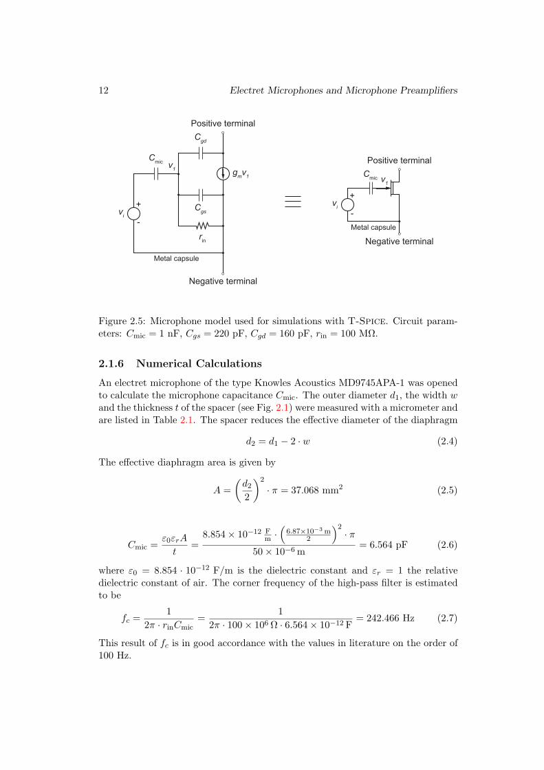
A complete microphone model (including the JFET) for use in T-Spice was pro-vided by Michael Baker, one of the authors of [3] and is shown in Fig. 2.5. Asdescribed in [8], the electrical representation of a capacitive sensor consists of anequivalent small-signal voltage source vi in series with a source capacitor Cmic (seeFig. 2.5). It is also pointed out that audio microphones need high-pass filteringwith a cut-off frequency around 100 Hz to attenuate large low-frequency signals.Reportedly, the input impedance rin of a typical JFET is around a few 100 MΩand results together with a typical gate-to-source capacitance Cgs in a high-passcorner frequency of a few 100 Hz. Calculations carried out in Subsection 2.1.6 showa rough estimation for the corner frequency fc on the order of 242.466 Hz for theKnowles Acoustics MD9745APA-1 microphone.
2.1.5 Interfacing the Electret Microphone
The metallized electret foil diaphragm is contacted through a metal contact ringto the microphone capsule and connected to the source of the JFET. The metalbackplate is connected to the gate of the JFET. For the microphone of the typeKnowles Acoustics MD9745APA-1, these facts are indicated in the data sheet [10].A resistor can be switched in between the source of the JFET and ground to limitthe bias current of the JFET. However, Kurt Heutschi, lecturer for acoustics atETH, pointed out that the membrane does not need to be directly connected to thesource of the JFET and that other JFET buffer principles exist in literature. Forinstance, [3] uses a microphone model with a JFET in a common-drain configurationand a source resistor of Rs = 20 kΩ to buffer the gate voltage.
12 Electret Microphones and Microphone Preamplifiers
Cgs
Cgd
rin
Cmic
vi
+
-
Negative terminal
Positive terminal
gmv1
v1
vi
Cmic
+
-
v1
Positive terminal
Negative terminal
Metal capsule
Metal capsule
Figure 2.5: Microphone model used for simulations with T-Spice. Circuit param-eters: Cmic = 1 nF, Cgs = 220 pF, Cgd = 160 pF, rin = 100 MΩ.
2.1.6 Numerical Calculations
An electret microphone of the type Knowles Acoustics MD9745APA-1 was openedto calculate the microphone capacitance Cmic. The outer diameter d1, the width wand the thickness t of the spacer (see Fig. 2.1) were measured with a micrometer andare listed in Table 2.1. The spacer reduces the effective diameter of the diaphragm
d2 = d1 − 2 · w (2.4)
The effective diaphragm area is given by
A =(d2
2
)2
· π = 37.068 mm2 (2.5)
Cmic =ε0εrA
t=
8.854× 10⁻¹² Fm ·(
6.87×10⁻³ m2
)2· π
50× 10−6 m= 6.564 pF (2.6)
where ε0 = 8.854 · 10−12 F/m is the dielectric constant and εr = 1 the relativedielectric constant of air. The corner frequency of the high-pass filter is estimatedto be
fc =1
2π · rinCmic=
12π · 100× 106 Ω · 6.564× 10−12 F
= 242.466 Hz (2.7)
This result of fc is in good accordance with the values in literature on the order of100 Hz.
2.2 Experiments 13
d1 8.87 mmw 1 mmd2 6.87 mmd 8 mmt 50 µmCmic 6.564 pFfc 242.466 Hz
Table 2.1: Measured dimensions and circuit parameters of the microphone (KnowlesAcoustics MD9745APA-1).
Part Producer NumberOperational amplifier National Semiconductor LMC6484INN-type JFET Fairchild Semiconductor BF244A/BP-type MOSFET Vishay Siliconix BS250Electret microphone Knowles Acoustics MD9745APA-1
Table 2.2: Discrete components used for the experiments on the proto board.
2.2 Experiments
The main results arising from experiments with the electret microphone, the JFETand the microphone preamplifier as described in [3] are presented. A microphoneof the type Knowles Acoustics MD9745APA-1 was used for the experiments (seeTable 2.2). Its typical sensitivity is −41 dB which corresponds to 8.913 mV/Pa(note that 0 dB = 1 V/Pa) [10].
2.2.1 Electret Microphone
In the first experiment, resistors Rs of different values were connected betweenthe negative terminal of the microphone and ground and the bias currents weremeasured. The plots are shown in Fig. 2.6. Qualitatively, the source resistor causesa voltage drop which in turn reduces the effective drain-to-source voltage Vds of theJFET and thus the bias current of the microphone.
It turns out that the linear (or triode) region of the JFET is further extendedfor higher drain-to-source voltages, which means that for the same drain-to-sourcevoltage the JFET is made to operate in the linear region when a source resistor isadded. In this way the bias current of the microphone is drastically reduced andmore linearity is achieved. It is important to note that switching in a source resistorhas no effect on the gate-to-source voltage Vgs of the JFET.
Access to internal nodes of the microphone was not possible because charge onthe gate of the JFET would leak away and noise might be coupled into the high-

14 Electret Microphones and Microphone Preamplifiers
0 0.5 1 1.5 2 2.5 3 3.50
50
100
150
200
250
Vds
(V)
I ds (μ
A)
Rs = 0 Ω
Rs = 2.2 kΩ Rs = 4.7 kΩ Rs = 8.2 kΩ
Rs = 22 kΩ
Figure 2.6: Plot of the microphone currents for different source resistors as a func-tion of the voltage between the microphone terminals. A comparison between thecurves shows that the linearity in the triode region is increased with higher sourceresistors.
impedance node. Also, the small-signal parameters of the JFET, like parasitic gate-to-source Cgs and gate-to-drain Cgd capacitance could not easily be characterized.
2.2.2 Microphone Preamplifier
A setup of the microphone preamplifier proposed in [3] was built of discrete circuitelements (see Table 2.2) on a proto board. Refer to Fig. 3.2 in Chapter 3 for aschematic of the circuit. The OTA for adaptation was replaced with an OpAmpand a high resistor in the order of 1 MΩ in series with the OpAmp output. Theamplification and the DC adaptation mechanism could be experimentally verified.However, it is not sure how reliable the results are because only high-voltage MOS-FETs were provided.
A slightly different value for the transconductance parameter β resulted fromthe experiments and was incorporated into the nJFET model in T-Spice. β wasdoubled and now is equal to 6× 10⁻⁵ A/V2.
2.3 Preamplifier with Controllable Feedback Resistor
In the context of a binaural silicon cochlea chip designed by Shih-Chii Liu, wealso designed and laid out a microphone preamplifier based on [3], which uses a

2.3 Preamplifier with Controllable Feedback Resistor 15
A
Gm
Imic,AC
Rf
Vo
vi
+
-
Cmic
M1
M2
Vref
+
-
+
-
+
-
Cad
Imic,DC
nOTA
OpAmp
Electret microphone
Vdd
Figure 2.7: Schematic of the microphone preamplifier with controllable feedbackresistor.
controllable feedback resistor. The schematic of the circuit is shown in Fig. 2.7.The working principle of the microphone preamplifier is discussed in Section 3.1 ofChapter 3 in detail. Since electret microphones come in a great variety with cheapand expensive types differing in their sensitivity, it was desirable to implement amicrophone preamplifier with a variable feedback resistor, and thus variable gainto adjust the amplitude of the AC voltage at the output. A sketch of the variableresistor is shown in Fig. 2.8.
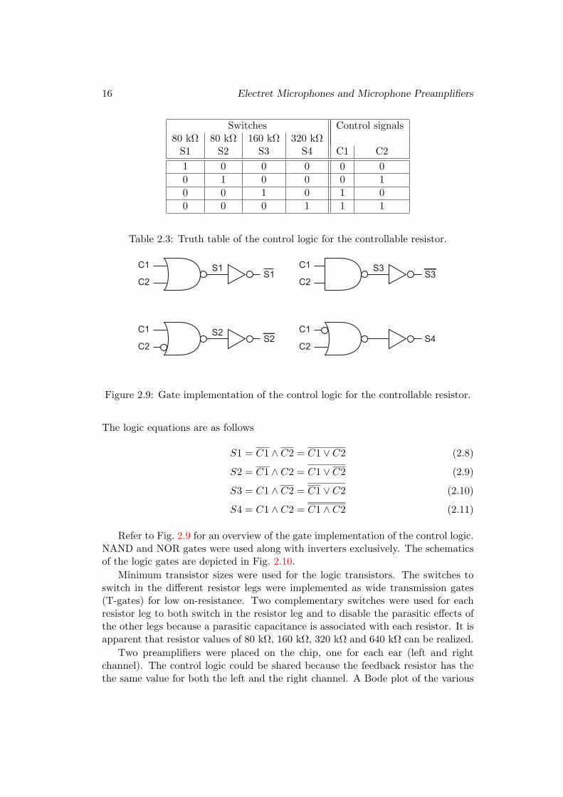
The control logic was implemented according to the truth table in Table 2.3.
R1 = 80 kΩ
S1 S2 S3 S4
S1 S2 S3
R2 = 80 kΩ R3 = 160 kΩ R4 = 320 kΩ
Rf
Figure 2.8: Schematic of the controllable resistor. S1 closed corresponds to 80 kΩ,S2 closed corresponds to a total 160 kΩ, S3 closed corresponds to a total 320 kΩ,S4 closed corresponds to a total 640 kΩ.
16 Electret Microphones and Microphone Preamplifiers
Switches Control signals80 kΩ 80 kΩ 160 kΩ 320 kΩ
S1 S2 S3 S4 C1 C21 0 0 0 0 00 1 0 0 0 10 0 1 0 1 00 0 0 1 1 1
Table 2.3: Truth table of the control logic for the controllable resistor.
C1
C2
C1
C2
C1
C2
C1
C2
S1
S2S2
S1S3
S4
S3
Figure 2.9: Gate implementation of the control logic for the controllable resistor.
The logic equations are as follows
S1 = C1 ∧ C2 = C1 ∨ C2 (2.8)
S2 = C1 ∧ C2 = C1 ∨ C2 (2.9)
S3 = C1 ∧ C2 = C1 ∨ C2 (2.10)
S4 = C1 ∧ C2 = C1 ∧ C2 (2.11)
Refer to Fig. 2.9 for an overview of the gate implementation of the control logic.NAND and NOR gates were used along with inverters exclusively. The schematicsof the logic gates are depicted in Fig. 2.10.
Minimum transistor sizes were used for the logic transistors. The switches toswitch in the different resistor legs were implemented as wide transmission gates(T-gates) for low on-resistance. Two complementary switches were used for eachresistor leg to both switch in the resistor leg and to disable the parasitic effects ofthe other legs because a parasitic capacitance is associated with each resistor. It isapparent that resistor values of 80 kΩ, 160 kΩ, 320 kΩ and 640 kΩ can be realized.
Two preamplifiers were placed on the chip, one for each ear (left and rightchannel). The control logic could be shared because the feedback resistor has thethe same value for both the left and the right channel. A Bode plot of the various

2.4 Novel Approaches for Low-Power Audio Amplifiers 17
Vdd
INP1
INP1
INP2
INP2
OUPOUP
Vdd
INP2
INP1
INP1 INP2
NAND gate NOR gate T-gate
INP OUP
Si
Si
Figure 2.10: Logic gates used in the control logic.
transfer functions for different values of the feedback resistor Rs with Cad = 6 pFand Rs = 0 Ω is shown in Fig. 2.11.
Fabrication will be done in the MOSIS 0.35 µm CMOS process where four metaland two poly silicon layers are available. The designed layout is shown in Fig. 2.12.
2.4 Novel Approaches for Low-Power Audio Amplifiers
The requirements for a microphone preamplifier can be summarized as follows:
• The drain-to-source voltage Vds of the JFET and the output voltage of thepreamplifier must be decoupled, i.e. both the voltage across the JFET and theDC level of the output voltage of the preamplifier can be set independently.
• High power-supply rejection ratio (PSRR) because the device will be batterypowered and devices such as motors can cause large transient supply drops.
• Low power consumption.
• Wide dynamic range.
• Current-mode adaptation with an adaptive element to separate the DC andAC components of the microphone current.
• Non-custom design, i.e. every electret microphone can be used.
• Amplification of the signal across a resistor for current-to-voltage conversion.An active circuit element in a feedback configuration is required for the am-plification.
• A stable operating point has to be reached after power-up within a fractionof a second.

18 Electret Microphones and Microphone Preamplifiers
100 101 102 103 104 105 106-40
-20
0
20
40
Frequency (Hz)
Mag
nitu
de (d
B)
100 101 102 103 104 105-200
-150
-100
-50
0
50
100
150
200
Frequency (Hz)
Pha
se (d
eg)
Rf = 640 kΩRf = 320 kΩRf = 160 kΩRf = 80 kΩ
Rf = 640 kΩRf = 320 kΩRf = 160 kΩRf = 80 kΩ
Figure 2.11: Bode plot of the transfer function of the preamplifier with controllablefeedback resistor showing the gain and phase from the equivalent microphone ACsignal voltage source to the preamplifier output. Circuit parameters: Cad = 6 pF,Rs = 0 Ω, Ib1,OA = 30 nA, Ib2,OA = 1 µA, Ib,OTA = 1 pA.

2.4 Novel Approaches for Low-Power Audio Amplifiers 19
Figure 2.12: Chip layout.

20 Electret Microphones and Microphone Preamplifiers
2.4.1 Architecture of the Microphone Preamplifier
Conventional microphone preamplifiers like [3] operate with a huge microphonebias current in the order of 220 µA at a 3.3 V power supply and consume too muchpower. A way to trade signal-to-noise ratio (SNR) versus power in the microphonepreamplifier based on [3] is to dynamically control a resistor between the negativeterminal of the microphone and ground. Because sound and speech correlate, it isconceivable to switch between two modes differing in the source resistance: An ultralow-power mode (huge source resistor) with reduced bias current and sensitivitywhich is capable of detecting sound and a normal low-power mode (ordinary sourceresistor) with standard circuit operation which amplifies the microphone signal forspeech processing.
Circuit operation after power-up starts in the ultra low-power mode. As soon assound is detected, the circuit switches to the high-sensitivity mode which is appro-priate to detect speech. After a time-out that is set by a leakage transistor in thesound detector, the high-sensitivity mode is left and the microphone preamplifierreturns into the low-sensitivity mode. Fig. 2.13 illustrates the basic architecture ofthe microphone preamplifier including the sound detector.
2.4.2 Sound Detector
An OpAmp in the sound detector first compares the voltage at the microphonepreamplifier output Vin with a threshold voltage Vth (see Fig. 2.14). If the signalvoltage exceeds the threshold voltage, the capacitor C is charged through the diode-connected transistor M1 which is forward biased. Note that capacitor C cannot bedischarged through M1. The capacitor voltage VC is shifted by the source follower,consisting of transistors M3 and M4. Once the capacitor voltage reaches a certainlevel the first inverter switches to the complementary state. Two more invertersfollow to make steeper edges and in order to generate the signals Ctrl and Ctrl tocontrol the transmission gates (T-gates) which in turn switch in resistor R1 or R2.
A time-out function is implemented by continuously discharging capacitor Cthrough the leakage transistor M2. When the capacitor voltage VC falls below acertain level, the first inverter switches back to the complementary state. The in-verters are implemented as starved inverters because otherwise the newly conservedpower is wasted due to high switching currents.
Even when the microphone preamplifier operates in the ordinary low-powermode, it takes the circuit after power-up on the order of three seconds to settleto the DC operating point. Each time sound is detected in the ultra low-powermode and the circuit switches to the high-sensitivity mode, however, it takes theadaptive element a couple of seconds to adapt to the new microphone bias currentbecause the capacitor Cad has to be charged by the low-transconductance nOTA.This problem has not been resolved yet. A workaround may consist of also switchingin a higher bias current source in the OTA.

2.4 Novel Approaches for Low-Power Audio Amplifiers 21
A
Gm
Imic,AC
Rf
Vo
vi
+
-
Cmic
M1
M2
Vref
+
-
+
-
Cad
v1
Imic,DC
nOTA
OpAmp
Electret microphone
Vdd
R1 R2
Sounddetector VthT1 T2
Figure 2.13: Schematic of the microphone preamplifier including the sound detector.
A+
-
OpAmp C
Vdd
M3
M4Vsf
Ctrl
Ctrl
M1
M2Vleak
Vth
Vin
Ileak
VC
Figure 2.14: Possible implementation of the sound detector.

22 Electret Microphones and Microphone Preamplifiers

Chapter 3
Design of the Speech Detector
In this chapter we discuss the implementation of the speech detector with sub-threshold analog circuits. The design aims at the MOSIS 1.6 µm process with apower supply of Vdd = 3.3 V. It should not use more area than a half of a MOSISTinyChip (2.2 × 2.2 mm2) because a face detection sensor will also be placed onthe chip. The key figure of merit is the power consumption. The chip should bepowered with an AA battery for about a year. The design must interface a mi-crophone at the input and provide a digital output to a microcontroller. It mustbe able to bias itself without external components on the board. The order of thesections follows the signal processing from the input to the output (see Fig. 3.1).An overview of the signal processing algorithm is given in Section 1.5 in Chapter1. Finally, the bias generator is addressed before concluding with the results of thechip-level simulation of the full speech detection circuit.
Speech bandpower
100 Hz-2 kHzSpeech band
V2 I3 I4I1
Low-powermicrophonepreamplifier
Antibumpcircuit
1st orderlog-domainband-pass
filter
Class-Bcurrent mirror
Have-waverectifier
2-16 Hzphoneme band
Neuron
Vs
I5
Microphone
Detectedspeech
Figure 3.1: Circuit architecture of the speech detector showing the individual build-ing blocks. The arrows at the interface of two blocks indicate whether it is a voltageor current input/output.

24 Design of the Speech Detector
3.1 Microphone Preamplifier
The preamplifier chosen for implementation (see Fig. 3.2) is based on Baker andSarpeshkar’s circuit [3] which shows advantages in power-supply rejection ratio(PSRR), a high gain and a relatively low power consumption. It separates theDC and AC components of the microphone current and converts the small-signalcurrent into a voltage across the feedback resistor.
Fig. 3.2 shows a schematic of the microphone preamplifier. The design containsa low-frequency feedback loop to adapt to the DC bias current Imic,DC of the mi-crophone. The DC bias current is sensed by the adaptive element and sourced bythe pFET, M2, whereas the AC current Imic,AC is fed through the feedback resistorRf . The AC current is sensed with a sense-amplifier configuration and convertedinto an AC voltage across the feedback resistor with the DC voltage componentdetermined by the reference voltage at the non-inverting input of the OpAmp. In-tuitively, subtracting the DC component of the total signal, combined with thefinite bandwidth of the circuit leads to a transfer characteristic with the shape ofa band-pass filter.
3.1.1 Operational Amplifier (OpAmp)
The p-type OpAmp is implemented as a simple Miller OpAmp. It should be capableof driving off-chip loads in the order of 1 pF or even more. The cutoff frequency canbe changed by varying the Miller capacitor CM . A higher CM moves the dominantpole to lower frequencies. In this design, a Miller capacitor of CM = 300 fF waschosen.
A large transistor length L in the OpAmp input stage improves matching andmakes a high Early voltage for high gain. The aspect ratios of the transistors inthe OpAmp were directly taken from the OpAmp presented in [3].
The OpAmp was simulated in a feedback configuration with a feedback resistorof 1 GΩ between the output and the inverting input and a load capacitor of CL =2 pF to explore pseudo-open loop characteristics. This configuration results in aextremely high time constant of the feedback path. The inverting input was coupledto ground through a 1 F capacitor. The DC voltage at the non-inverting input was1.3 V. The simulation results are illustrated in the Bode plot of Fig. 3.3.
A cutoff frequency of fp,OA = 400 mHz and a DC voltage gain of ADC,OA =116.68 dB were found. We assume that the gain function A(s) of the operationalamplifier contains a single pole
A(s) =ADC,OA
1− spOA
=ADC,OA
1 + s · τp,OA(3.1)
where ADC,OA is the low-frequency gain and τp,OA is the time constant of the poleof the OpAmp. The gain-bandwidth product of the OpAmp is given by
GBPOA = ADC,OA · |pOA| = ADC,OA · 2πfOA = 1.7149 MHz (3.2)

3.1 Microphone Preamplifier 25
Cmic
rin gm1v1vi
+
-
v1
vo=-A(s)v2
Rf
v2
Gm(v2-vo)gm2v3 Cad
v3
+
-
A(s)
Gm
Imic,AC
Rf
Vo
vi
+
-
Cmic
M1
M2
Vref
+
-
+
-
+
-
Cad
v2
v3
v1
Imic,DC
nOTA
OpAmp
Adaptive element
Electret microphone
Vdd
(a)
(b)
Figure 3.2: (a) Circuit topology of the microphone preamplifier including a p-typeOpAmp, an n-type OTA and an adaptive element. Note that a resistance Rs can beswitched in between the source of the JFET and ground to reduce the bias currentof the JFET and thus the power consumption. (b) Small-signal equivalent circuitas used for the derivation of the transfer function of the microphone preamplifier.

26 Design of the Speech Detector
10-1 100 101 102 103 104 105 106
0
20
40
60
80
100
120
Frequency (Hz)
Mag
nitu
de (d
B)
Simulation dataTheoretical form
10-1 100 101 102 103 104 105 106-300
-250
-200
-150
-100
-50
0
Frequency (Hz)
Pha
se (d
eg)
Simulation dataTheoretical form
Figure 3.3: Gain magnitude and phase versus frequency for the operational ampli-fier (OpAmp). The simulation shows that the assumption of a dominant pole atlow frequencies and the approximation of the gain function below 1 kHz are valid.

3.1 Microphone Preamplifier 27
For proper large-signal behavior it is important that the output stage of theMiller OpAmp can provide at least the AC signal current of the microphone. Oth-erwise, the differential input voltage cannot be balanced to be zero and the OpAmpstarts to slew causing clipping of the AC signal.
3.1.2 Operational Transconductance Amplifier (OTA)
A simple 5-transistor low-current n-type OTA (nOTA) with an aspect ratio ofW/L = 6λ/24λ was chosen for implementation. A large transistor length L in-creases the gain because it effects in a higher output resistance. As another benefit,transistor mismatch has less influence on the circuit behavior. The OTA is a differ-ential to single-ended transconductor and determines in the context of the adaptiveelement the pass-band in the transfer function of the microphone preamplifier.
3.1.3 Adaptive Element
The capacitor for adaptation is equal to Cad = 10 pF. AC analysis and detailedcalculations of the transfer function of the preamplifier in Appendix A have shownthat the pFET of the adaptive element, M2, affects the cutoff frequency of theband-pass characteristic. A wide and short transistor was chosen to set the cutofffrequency around 2 kHz. As a side effect, the parasitic capacitances Cgs and Cgbof M2 increase the effective capacitance Cad,tot of the adaptive element. Therefore,the total capacitance contributing to the adaptation is given by
Cad,tot = Cad + Cgs2 + Cgb2 = 11.225 pF (3.3)
3.1.4 Simplified Analysis of the Transfer Function
Here we analyze the small-signal transfer function of the microphone preamplifierfrom the equivalent microphone input voltage source vi to the preamplifier out-put vo. Second-order effects, such as channel-length modulation (or Early effect),which leads to finite output resistance, and parasistic node capacitance, are ne-glected. Furthermore, the impedance between the source of the microphone JFETand ground is not considered. The small-signal equivalent circuit is depicted inFig. 3.2.
Since Cmic and rin form a voltage divider across vi, the gate-to-source voltageof the JFET is given by
v1 = vi ·rin
1sCmic
+ rin(3.4)
The output voltage of the OpAmp is
vo = −A(s) · v2 (3.5)

28 Design of the Speech Detector
where A(s) is the gain of the OpAmp open-loop transfer function. Assuming thatthe OpAmp has a dominant pole, from Eq. (3.1) the OpAmp transfer function (orgain) is
A(s) =ADC,OA
1 + s · τp,OA(3.6)
where ADC,OA is the low-frequency voltage gain and τp,OA is the time constant ofthe pole of the OpAmp. From Kirchhoff’s current law (KCL) at node v2
−gm1v1 − gm2v3 −1 +A(s)Rf
v2 = 0 (3.7)
Kirchhoff’s voltage law (KVL) at node v3 gives
v3 = Gm(v2 − vo) ·1
sCad(3.8)
Solving Eq. (3.5) for v2 = −v0/A(s), substituting it together with Eq. (3.8) intoEq. (3.7) gives
− gm1rin1
sCmic+ rin
vi +Gmgm2
(1 + 1
A(s)
)sCad
vo +1 + 1
A(s)
Rfvo = 0 (3.9)
The transfer function from the equivalent microphone AC signal voltage source vito the preamplifier output vo is given by
H(s) =v0
vi=
gm1rin1
sCmic+rin
Gmgm2
“1+ 1
A(s)
”sCad
+1+ 1
A(s)
Rf
(3.10)
Rearranging and multiplying nominator and denominator by Rf/rin gives
H(s) =gm1Rf(
Gmgm2RfsCad
+ 1)(
1sCmicrin
+ 1)(
1 + 1A(s)
) (3.11)
Substituting the gain of the OpAmp A from Eq. (3.6) into the previous equationyields
H(s) =gm1Rf(
Gmgm2RfsCad
+ 1)(
1sCmicrin
+ 1)(
1 + 1+sτp,OA
ADC,OA
) (3.12)
The term (1 + 1/A(s)) can be rewritten as
1 +1
A(s)=ADC,OA + 1 + sτp,OA
ADC,OA=ADC,OA + 1ADC,OA
(1 + s
τp,OA
ADC,OA + 1
)(3.13)

3.1 Microphone Preamplifier 29
Hence, the transfer function from Eq. (3.12) simplifies to
H(s) =gm1Rf
ADC,OA
ADC,OA+1(Gmgm2RfsCad
+ 1)(
1sCmicrin
+ 1)(
1 + sτp,OA
ADC,OA+1
) (3.14)
=HPB(
1sτp1
+ 1)(
1sτp2
+ 1)
(1 + sτp3)(3.15)
where
HPB = gm1RfADC,OA
ADC,OA + 1(3.16)
τp1 = Cmicrin (3.17)
τp2 =Cad
Gmgm2Rf(3.18)
τp3 =τp,OA
ADC,OA + 1(3.19)
H(s) is the transfer function from the equivalent microphone AC signal voltagesource vi to the preamplifier output vo. HPB is the voltage gain in the pass-band(or in-band voltage gain). It is obvious that τp1 corresponds to the pole at lowfrequencies caused by the electret microphone capacitor Cmic and the huge inputresistance rin of the JFET as discussed in Subsection 2.1.4 of Chapter 2. The secondpole τp2 is due to the presence of the adaptive element, formed by the capacitor Cadand the transconductance Gm of the nOTA. Because of the feedback configuration,the pole of the OpAmp τp3 is moved to much higher frequencies. That is not asurprise because gain is traded for bandwidth.
However, the foregoing analysis is not accurate as far as the high-frequencybehavior of the circuit (i.e. the pole causing the rolloff) is concerned. It is shownin Appendix A that the bandwidth limiting factor is mainly capacitive couplingthrough the gate-to-drain capacitance Cgd2 of the pFET, M2, of the adaptive ele-ment. As a consequence, a small-signal current is generated by gm2 which causes afinite resistance, looking into the pFET. The equivalent resistance Req forms in con-junction with the feedback resistor Rf a voltage divider across the OpAmp whichdecreases the fraction of the voltage from the output of the OpAmp that is fedback to the inverting input of the OpAmp. This effect substantially reduces thebandwidth of the circuit. Thus, the pole causing the rolloff is given by
p3 = −ADC,OA(Cad,tot + Cgd2)
τp,OACgd2gm2Rf= −
GBPOA(Cad,tot + Cgd2)Cgd2gm2Rf
(3.20)
where Cad,tot is the effective capacitance of the adaptive element and GBPOA isthe gain-bandwidth product of the OpAmp. The simulation parameters can befound in Table 3.1. The simulations were done with a microphone model providedby Michael Baker, one of the authors of [3], including a microphone capacitor ofCmic = 1 nF.

30 Design of the Speech Detector
OpAmpIb1,OA = 46.8 nAIb2,OA = 11 µACM = 300 fF
ADC,OA = 116.68 dBfp,OA = 400 mHz
GBPOA = 1.7149 MHzVref = 1.3 V
OTAIb,OTA = 7.69 pA
κ = 0.7Gm = 105.96 pSRo = 9.0416× 10¹² Ω
JFETgm1 = 247µSgds1 = 15µSCgs1 = 220 pFCgs1 = 160 pF
pFETgm2 = 1.24 mSgds2 = 3µSCgs2 = 415 fFCgd2 = 6.57 pFCgb2 = 810 fF
Cmic = 1 nFrin = 100 MΩRf = 300 kΩCad = 10 pF
Cad,tot = 11.225 pF
Table 3.1: (Small-signal) circuit parameters of the microphone preamplifier ex-tracted from T-Spice.
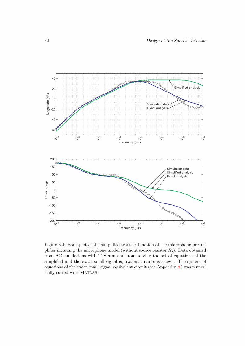
3.1.5 Numerical Calculations
Fig. 3.4 shows the Bode plot of the transfer characteristic of the microphone pream-plifier obtained from AC simulations with T-Spice together with the plots of theanalytically derived transfer functions. The small-signal parameters extracted fromT-Spice were used for the calculation of the pass-band gain and the pole frequen-cies of the analytical expression (see Table 3.1). Evaluation of Eqs. (3.16) to (3.19)gives
HPB = gm1RfADC,OA
ADC,OA + 1= 37.3964 dB (3.21)
fp1 =1
2πτp1=
12πCmicrin
= 1.5915 Hz (3.22)
fp2 =1
2πτp2=Gmgm2Rf
2πCad= 627.3429 Hz (3.23)
fp3 =1
2πτp3=
1 +ADC,OA
2πτp,OA= 272.94 kHz (3.24)
HPB is the pass-band gain of the preamplifier, fp1 is the frequency of the first polecaused by the microphone, fp2 is the frequency of the second pole caused by theadaptive element and fp3 is the frequency of the pole due to the finite bandwidthof the OpAmp. It can be seen that the calculations of the low-frequency poles arein good agreement with those derived from the simulation data. Note that second-order effects such as channel-length modulation and parasitic capacitance have notbeen considered.
A more elaborate analysis of the microphone preamplifier in Appendix A shows

3.2 Squaring Circuit 31
that from Eq. (A.31) the pole frequency of the third pole is given by
fp3 =|p3|2π
=ADC,OA(Cad,tot + Cgd2)
2πτp,OACgd2gm2Rf= 1.9872 kHz (3.25)
3.2 Squaring Circuit
The squaring circuit consists of an adaptive element to obtain the DC level of theinput voltage and an antibump circuit [12] which performs the actual squaringoperation. A circuit schematic of the squaring circuit is shown in Fig. 3.5.
3.2.1 Adaptive Element
The voltage of the speech signal at the preamplifier output has to be squared todetermine the power of the signal. Because the differential input of the squaringcircuit is squared, one input to the antibump circuit has to adapt to the DC level ofthe other input. Ideally, the DC level is equal to the reference voltage at the non-inverting input of the OpAmp, however, because of voltage offsets in the OpAmpand the OTA of the previous preamplifier stage, the DC level in the physical circuitmight slightly differ from the ideal value. That is the reason why an adaptiveelement is required. The ideal adaptive element has a characteristic of a low-passfilter with a high time constant to cause a cutoff frequency at least below the lowestfrequency of the speech band around 100 Hz.
The proposed adaptive element from [13] could not be used because the as-sociated RC time constant was too long. It led to an excessive settling time ofthe circuit after power-up that cannot be tolerated. It was replaced with a simplefollower integrator circuit consisting of an p-type OTA (pOTA) and a capacitor C.As described in [11] (p. 252), the equivalent transconductance is
G =κIb2UT
(3.26)
where κ is the subthreshold slope factor, Ib the bias current of the OTA and UT =kT/q = 25.4 mV the thermal voltage. The time constant is given by
τ =C
G(3.27)
The cutoff frequency is equal to
fc =1
2πτ=
G
2πC=
κIb4πUTC
(3.28)
With C = 1 pF and Ib = 1 pA, this yields a cutoff frequency of fc = 140 Hz.The cutoff frequency of the follower integrator has to be below 100 Hz in order tofunction as an adaptive element.
32 Design of the Speech Detector
10-1 100 101 102 103 104 105 106
-60
-40
-20
0
20
40
Frequency (Hz)
Mag
nitu
de (d
B)
10-1 100 101 102 103 104 105 106-200
-150
-100
-50
0
50
100
150
200
Frequency (Hz)
Pha
se (d
eg)
Simulation dataExact analysis
Simplified analysis
Simulation dataSimplified analysisExact analysis
Figure 3.4: Bode plot of the simplified transfer function of the microphone pream-plifier including the microphone model (without source resistor Rs). Data obtainedfrom AC simulations with T-Spice and from solving the set of equations of thesimplified and the exact small-signal equivalent circuits is shown. The system ofequations of the exact small-signal equivalent circuit (see Appendix A) was numer-ically solved with Matlab.

3.2 Squaring Circuit 33
Gm
+
-
pOTA V1
V2
V2
V1V2
Ib
C
V1=VDC
Vin=V2
Isum
mirror to next stage
Vdd
Adaptive element
Figure 3.5: Schematic of the squaring circuit including the adaptive element. Cir-cuit parameter: C = 1 pF.

34 Design of the Speech Detector
V1
V2V1
Ib
Isum
Vc
I1 I2
M1 M3
M4
Imid
M2
Middle legOuter leg
Vd1
Vdd
Figure 3.6: Schematic of the antibump circuit (simplified).
3.2.2 Antibump Circuit
A circuit capable of performing a squaring operation on the signal is needed todemodulate the speech signal back to the baseband and to compute its power.Antibump circuits as described in [12] are well-suited for that purpose because theyfeature an V –I input-to-output characteristic which is very similar to a parabola.In the following, the V –I characteristic is derived for a p-type antibump circuit.
The strength ratio is the ratio of the aspect ratio of the transistors in the middleleg, M3 and M4, to the aspect ratio in the outer legs, M1 and M2. This parameteris given by
S =(W/L)middle
(W/L)outer(3.29)
and is used for the derivation of the circuit equations. In the analysis of the circuit,it is assumed for the sake of simplicity that the transistors in the outer legs are unittransistors and that the transistors in the middle leg are scaled by a factor S.
Fig. 3.6 shows the simplified antibump cicuit. It has three outputs: I1, I2 andImid. For the squaring function we are solely interested in the antibump outputwhich is formed by combining the currents of the outer legs Isum = I1 + I2. Quali-tatively, we can understand the operation of the antibump circuit as follows: Dueto Kirchhoff’s current law (KCL), the three currents, I1, I2 and Imid, must sum tothe bias current Ib. Therefore, the voltage Vc follows the lower of V1 or V2.
As described in [11] (p. 170–175), current flows through all three legs of thecircuit, if no differential voltage is applied ∆V = 0. When |∆V | increases, thecommon-node voltage Vc follows the lower of V1 or V2 and cuts off Imid, becausethe transistor whose gate is connected to the higher of V1 or V2 shuts off. If bothV1 and V2 fall together, Imid does not increase, because the common-node voltageVc decreases along with V1 and V2.

3.2 Squaring Circuit 35
The general I–V equation for a pFET is [11] (p. 70)
I = I0 eκ(Vw−Vg)
(e−(Vw−Vs) − e−(Vw−Vd)
)(3.30)
where Vw is the bulk voltage of the MOSFET. To reduce common mode short andnarrow channel effects, all pFET bulks are connected to their sources.
The transistors of the outer leg, M1 and M2, operate in the subthreshold satu-ration region. Hence, the currents I1 and I2 are given by1
I1 = I0 eκ(Vc−V1), I2 = I0 e
κ(Vc−V2) (3.31)
Transistors M3 and M4 of the middle leg work in the subthreshold triode andsaturation region, respectively
I3 = S · I0 eκ(Vc−V1)
(1− e−(Vc−Vd1)
)= S · I0
(eκ(Vc−V1) − eκ(Vc−V1)−(Vc−Vd1)
)(3.32)
I4 = S · I0 eκ(Vc−V2)−(Vc−Vd1) = S · I0 e
κ(Vc−V2) · e−(Vc−Vd1) (3.33)
Assuming that the currents through transistors M3 and M4 are identical I3 = I4 =Imid, and solving Eqs. (3.32) and (3.33) for e−(Vc−Vd1) yields
e−(Vc−Vd1) =eκ(Vc−V1)
eκ(Vc−V1) + eκ(Vc−V2)(3.34)
Substituting the term from Eq. (3.34) into Eq. (3.33) and from Kirchhoff’s currentlaw (KCL)
Ib = I1 + I2 + Imid (3.35)
= I0 eκ(Vc−V1) + I0 e
κ(Vc−V2) + S · I0 eκ(Vc−V2) eκ(Vc−V1)
eκ(Vc−V1) + eκ(Vc−V2)(3.36)
⇒ eκVc =Ib
I0 · (e−κV1 + e−κV2) + S · I0e−κV1 ·e−κV2
e−κV1+e−κV2
(3.37)
The antibump outputs sum together to
Isum = I1 + I2 = Ib − Imid = I0 eκ(Vc−V1) + I0 e
κ(Vc−V2) (3.38)
=Ib
I0 + S · I0e−κV1 ·e−κV2
(e−κV1+e−κV2)2
(3.39)
Using V2=V1 −∆V , the term in the denominator of Eq. (3.39) can be simplified
e−κV1 · e−κV2
(e−κV1 + e−κV2)2 =eκ∆V
(1 + eκ∆V )2 (3.40)
1Note that the terminal voltages are given in units of the thermal voltage UT .

36 Design of the Speech Detector
Dividing the nominator and denominator of Eq. (3.40) by eκ∆V/2 yields
1(eκ∆V/2 + e−κ∆V/2
)2 =4
cosh2(κ∆V2 )
= 4 sech2
(κ∆V
2
)(3.41)
with cosh(x) =ex − e−x
2, sech(x) =
1cosh(x)
(3.42)
Using this relation, Eq. (3.39) can be simplified and we get
Isum =Ib
1 + S4 sech2
(κ∆V
2
) (3.43)
where the voltages are in UT units. UT = kT/q = 25.4 mV.When ∆V = 0, the cosh term is 1 and the antibump output sums to
Isum,DC = I1 + I2 =Ib
S4 + 1
(3.44)
This is the DC current component of the output signal of the squaring circuit andwill be removed in the subsequent band-pass stage.
The antibump output current ranges from the minimum value in Eq. (3.44) for∆V = 0 to the maximum value Ib when the middle branch is shut off. Hence,the dynamic range (the ratio of the maximum to the minimum current) is S
4 + 1(see Table 3.2). It is reported in [11] (p. 172) that for very large S, the bottomof the antibump output characteristic becomes very flat. This contrasts with therequirement of a characteristic of a parabolic curve and sets a ceiling on S.
Transient analysis in T-Spice has shown an AC signal amplitude at the pream-plifier output in the order of 250 mV. This sets the range of input voltages wherethe I–V characteristic should have a parabolic form and should not be saturated.Moreover, the DC current of the antibump circuit Isum,DC was minimized withoutlosing the quadratic shape. All these considerations led to the final strength ratioof S = 64. Fig. 3.7 shows the simulated sweep input-to-output characteristic of theantibump circuit. The theoretical form for Isum fits the data quite well.
Since the antibump circuit has a differential input, the circuit behavior is ap-proximately independent of the common-mode voltage or the DC level of the inputvoltage which is set by the reference voltage of the OpAmp of the preceding pream-plifier stage. In reality, the non-zero conductance of the bias transistor in thecurrent mirror causes a larger bias current with decreasing common-mode inputvoltage.
3.2.3 Practical Considerations
Because of short and narrow channel effects, doubling the length of a transistor isnot equal to putting two transistors in series. Therefore it is crucial to use unittransistors in series and parallel in the antibump circuit to implement a certain

3.2 Squaring Circuit 37
0.8 0.9 1 1.1 1.2 1.3 1.4 1.5 1.6 1.7 1.80
5
10
15
20
25
30
35
V2-V
1, V
1 held constant (V)
I sum
(nA
)
Simulation dataParabolic fitAntibump fit
Figure 3.7: Input-to-output I–V characteristic of the antibump circuit. The plotsshow data point from simulation with T-Spice together with a theoretical fit withthe antibump formula and a parabolic fit. V1 was held constant and V2 was sweptover a range from 0.8 V to 1.8 V. The theoretical fit with the antibump formula inEq. (3.43) was computed, using the parameters Ib = 29.5 nA, S = 64 and κ = 0.7.The parabolic fit is a result of computing the least-square fit of the simulation data.The theoretically fit curve of the antibump circuit and the simulation data arealmost a perfect match. Since the numerically fit parabola matches the simulationdata quite well, we conclude that the antibump circuit effectively approximates thesquaring function.

38 Design of the Speech Detector
Ib
M1
M2
I1
Vd1Vg
Vd2
I2
Vc Imid1
Vd1
Imid2
Vd2
V1
V1V2
V2
Ib
Vc
(a) (b)
VddVdd
Figure 3.8: Schematics of the middle and outer legs of the antibump circuit. (a)Multiple transistors of the outer leg in series. (b) Multiple middle legs in parallel.
strength ratio (here S = 64). Consequently, all unit transistors are affected bythese effects in the same way. The bulk is connected back to get rid of common-mode effects.
In the design of the antibump circuit, four transistors were put in series toincrease to overall transistor length L. The following analysis aims at showingqualitatively that connecting two transistors in series is equivalent to doubling thelength of a single transistor if the Early effect is neglected. Refer to Fig. 3.8 (a) fora sketch of the circuit topology under observation.
Obviously, the upper transistor, M1, operates in the subthreshold triode regionwhen the lower transistor, M2, is stacked on M1, and the equations for a transistorin the triode region apply. However, transistor M2 is in the saturation region asusual and its drain potential can be neglected in the equation2
I1 = I0 eκ(Vc−Vg)
(1− e−(Vc−Vd1)
), I2 = I0 e
κ(Vc−Vg)−(Vc−Vd1) (3.45)
Rearranging and substituting I2 into the equation for I1 in Eq. (3.45) gives
I1 = I0 eκ(Vc−Vg) − I2 (3.46)
Since the two transistors are stacked on each other, the drain currents must beidentical I1 = I2 = I and Kirchhoff’s current law (KCL) holds. This yields
I =I0
2eκ(Vc−Vg) (3.47)
2Note that the terminal voltages are given in units of the thermal voltage UT .

3.2 Squaring Circuit 39
Therefore, connecting two transistors in series is similar to doubling the length Lof a single transistor.
The following analysis examines the effect of multiple middle legs in the an-tibump circuit with interchanged gate voltages. Again, the result is of purely quali-tative nature because the Early effect is not taken into account. A major benefit ofthis circuit topology is the capability of balancing the Early effect and, especially,balancing it when the transistors are above threshold. The drain currents throughthe top and bottom transistors of the individual legs are given by3
Imid1 = S · I0 eκ(Vc−V1)
(1− e−(Vc−Vd1)
)= S · I0
(eκ(Vc−V1) − eκ(Vc−V1)−(Vc−Vd1)
)(3.48)
Imid1 = S · I0 eκ(Vc−V2)−(Vc−Vd1) (3.49)
Imid2 = S · I0 eκ(Vc−V2)
(1− e−(Vc−Vd2)
)= S · I0
(eκ(Vc−V2) − eκ(Vc−V2)−(Vc−Vd2)
)(3.50)
Imid2 = S · I0 eκ(Vc−V1)−(Vc−Vd2) (3.51)
The currents flowing through either leg must be equal according to KCL. Solvingfor e−(Vc−Vd1) and e−(Vc−Vd2) gives
e−(Vc−Vd1) =eκ(Vc−V1)
eκ(Vc−V1) + eκ(Vc−V2), e−(Vc−Vd2) =
eκ(Vc−V2)
eκ(Vc−V1) + eκ(Vc−V2)(3.52)
It is obvious by substituting the exponential terms in Eq. (3.52) into Eqs. (3.49)and (3.51) that Imid1 and Imid2 are identical
Imid1 = I0 · Seκ(Vc−V2)eκ(Vc−V1)
eκ(Vc−V1) + eκ(Vc−V2)(3.53)
Imid2 = I0 · Seκ(Vc−V1)eκ(Vc−V2)
eκ(Vc−V1) + eκ(Vc−V2)(3.54)
⇒ Imid1 = Imid2 (3.55)
Hence, doubling the number of middle legs is equal to doubling the width W of thetransistors of a single leg.
3.2.4 Calculation of the Circuit Parameters
The strength ratio of the bump-antibump circuit is
S =2 [legs] · 8 [M] · (24/6)[aspect ratio]
14 [stacked] · (24/6) [aspect ratio]
= 64 (3.56)
where M is the number of identical fingers of a transistor. Neglecting parasiticeffects, taking M fingers of the width W corresponds to an overall width of M ·W .
3Note that the terminal voltages are given in units of the thermal voltage UT .

40 Design of the Speech Detector
Ib = 32.768 nAS = 64
Isum,DC = 1.71 nADynamic range = 25.6491 dB
κ = 0.7UT = kT/q = 25.4 mV
Table 3.2: Circuit parameters of the antibump circuit.
A least-square fit of the simulation data with a second order polynomial wascomputed as depicted in Fig. 3.7. The antibump output can be approximated by
Isum(∆V ) = 1.7048× 10⁻⁹ + 0.7069× 10⁻³ · (∆V )2 A (3.57)
In fact, in the intermediate region, where the difference of the input voltages∆V = V1 − V2 is small, the antibump circuit computes an approximation of thesquare of the differential input voltage ∆V , plus a DC offset Isum,DC. The designparameters of the squaring circuit are summarized in Table 3.2.
3.3 Phoneme Band Filter
Current-mode circuits which can realize long time constants on the order of 1 s arerequired to filter the signal power in the phoneme band in the range of 2–16 Hz. Thebasic current-filtering topology examined here are first-order log-domain low-passfilters, as presented in [14], which are capable of fulfilling this requirement. Theoverall band-pass filtering function is achieved by consecutive low-pass and high-pass filters. As a matter of fact, the high-pass filter comprises of a circuit whichforms the high-pass filtered signal by building the difference between the originalinput signal and the low-pass filtered signal by means of current mirrors.
The low-pass filter must be followed by the high-pass filter (and not vice versa).In contrast to the high-pass filter, the low-pass filtered signal current comes witha DC component which is needed to add another filter stage. A pure AC signalcurrent, which results in the high-pass filter, could not be used for further process-ing. On the other hand, the input signal to the rectifier is ideally a pure AC signalwhich is either sourced or sunk by class-B current mirror.
3.3.1 Log-Domain Low-Pass Filter
The schematic of the selected first-order log-domain low-pass filter is shown inFig. 3.9. In the following, the theoretical analysis of a p-type circuit, consistingonly of pFETs, is shown, based on [14]. A p-type circuit topology has to be chosento respect the fact that the input current from the preceding stage is sunk by

3.3 Phoneme Band Filter 41
Ib1 Ib2
M1
M2 M3
M4
Iin
I3I2
I1 I4
Iout
ICCLPF
Vdd
Figure 3.9: Schematic of the first-order log-domain low-pass filter.
a simple n-type current mirror and to protect the low-current nodes from latercontamination from parasitic photocurrents [15] when this circuit is integrated withvision chips. As an advantage, the potentials of the n-wells can be set arbitrarily inthe single-tub target process to the respective source potential of the pFETs, thus,eliminating the κ-effect (backgate effect or body effect).
The lowpass filtering function is implemented by transistors M1–M4 and ca-pacitor CLPF. Additionally, cascode transistors could be used to keep the drainvoltages of M1 and M4 equal but were omitted in this design in order to reduce thecomplexity.
The basic assumption made is that the dynamics of the circuit are dominatedby the presence of the pole caused by CLPF. The poles originating from parasiticcapacitance at the input and output nodes are supposed to be at much higherfrequencies than the ones of interest. Assuming that all transistors, M1–M4, workin the subthreshold saturation region, the transistor equations are
I1 = I0 e−κVgs1/UT , I2= I0 e
−κVgs2/UT , (3.58)
I3 = I0 e−κVgs3/UT , I4 = I0 e
−κVgs4/UT (3.59)
where κ is the subthreshold slope factor (for a pFET), I0 is the transistor’s offcurrent (process dependent) and UT = kT/q = 25.4 mV is the thermal voltage [11].From Kirchhoff’s voltage law (KVL) around the loop Gnd, M1–M4, Gnd
Vgs1 + Vgs2 = Vgs3 + Vgs4 (3.60)
Multiplying the currents I1, I2 and I3, I4 gives the equations
I1 · I2 = I0 e−κ(Vgs1+Vgs2)/UT (3.61)
I3 · I4 = I0 e−κ(Vgs3+Vgs4)/UT (3.62)

42 Design of the Speech Detector
respectively. From Eq. (3.60), it is apparent that the two products in Eqs. (3.61)and (3.62) are equal, and the translinear equation for this circuit can be derived
I1 · I2 = I3 · I4 (3.63)
From Kirchhoff’s current law (KCL) at either the source or drain terminals ofthe transistors M1–M4,
I1 = Iin (3.64)I2 = Ib1 (3.65)I3 = Ib2 + IC (3.66)I4 = Iout (3.67)
and we find that the translinear equation (3.63) can be rewritten including thenewly found relations
Iout · (Ib2 + IC) = Iin · Ib1 (3.68)
The current through capacitor CLPF is
IC = CLPF · VC with (·) =ddt
(3.69)
Taking the first derivative with respect to time of I4 in Eq. (3.59), and substitutingI4 into the equation gives
I4 = I0 eκVC/UT ⇒ I4 =
I0κ
UTeκVC/UT · VC =
I4κ
UT· VC (3.70)
Solving Eq. (3.70) for VC and substituting it into Eq. (3.69) yields
VC =UTκ· I4
I4(3.71)
⇒ IC = CLPF ·UTκ· I4
I4(3.72)
As a consequence, substituting Eq. (3.72) into the translinear equation (3.68) andusing I4 = Iout results in the following time domain differential equation
Iout · Ib2 + IoutCLPF ·UTκ
= Iin · Ib1 (3.73)
Thus, the transfer function of the circuit in the Laplace domain is
HLPF(s) =Iout
Iin=
Ib1
Ib2 + sCLPFUTκ
=Ib1/Ib2
1 + sCLPFUTκIb2
(3.74)
=AI,dc
1 + sω0
with AI = Ib1/Ib2, ω0 = 2πf0 =1τ0
=κIb2
CLPFUT(3.75)

3.3 Phoneme Band Filter 43
Ib Ib
IinIout
CHPF
Vdd
Figure 3.10: Schematic of the first-order log-domain high-pass filter.
which describes a first-order low-pass filter with DC current gain AI,DC and 3-dBcutoff frequency ω0 = 1/τ0. It is evident that the DC current gain is given by theratio of the bias currents Ib1/Ib2 and that the time constant of the low-pass filteris governed by Ib2 only.
Solving Eq. (3.75) for the bias current Ib2, which determines the pole, gives
Ib2 =CLPFUTκτ0
=2πf0CLPFUT
κ(3.76)
Refer to Fig. 3.11 for a plot of the tranfer characteristic of the low-pass filter.
3.3.2 Log-Domain High-Pass Filter
The high-pass filter is implemented by taking the difference between the low-passfiltered input signal and the input signal itself (see Fig. 3.10). The filtered currentis ideally subtracted from a mirrored replica of the input current. As a side benefit,the carrier DC signal is removed by the subtraction and solely the AC signal is left.
Consequently, the transfer function of the low-pass filter has to be subtractedfrom one
HHPF(s) = 1−HLPF(s) (3.77)
Setting Ib1 = Ib2 = Ib in the transfer function of the low-pass filter HLPF(s),Eq. (3.74) results in the following Laplace domain transfer function
HHPF(s) =1−
(1 + s
ω0
)1 + s
ω0
= −sω0
1 + sω0
(3.78)
with ω0 = 2πf0 =1τ0
=κIb
CHPFUT(3.79)

44 Design of the Speech Detector
The zero corner frequency in the transfer function of the high-pass filter correspondsto the pole in the transfer function of the low-pass filter. Again, the bias currentIb is
Ib =CHPFUTκτ0
=2πf0CHPFUT
κ(3.80)
Refer to Fig. 3.11 for a Bode plot of the transfer characteristic of the high-passfilter.
Since the difference between a copy of the original signal and the output signalis built, it is crucial to obtain a unity DC current gain in the high-pass filter.Therefore, the two bias currents Ib1 and Ib2 must be equal. Transistor mismatchesand current inequalities might cause a deviation of the unity gain of the high-passfilter leading to DC offsets, which in turn can jeopardize the correct behavior of thefilter. As a remedy, a leakage transistor is incorporated in the neuron to eliminatethese offsets.
3.3.3 Log-Domain Band-Pass Filter
The first-order band-pass filter is built of a log-domain low-pass filter and a log-domain high-pass filter in series. Therefore, the overall band-pass filter frequencyresponse is determined by the product of the two transfer functions of the individualfilters
HBPF(s) = HLPF(s) ·HHPF(s) (3.81)
The bode plot of the tranfer function of the band-pass filter is depicted in Fig. 3.11.The bias currents of the band-pass filter and in general are powers of two of 1 pF.Independent of the accuracy of the size of the master bias current, the ratio ofthe corner frequencies of the band-pass filter and thus the bandwidth is preservedassuming that all the bias currents are off by the same amount.
3.3.4 Calculation of the Circuit Parameters
A trade-off between the capacitor area and the smallest current that the bias gen-erator can provide has to be made. The implication of Eqs. (3.75) and (3.79) isthat the larger we make the filter capacitor, the greater the bias current can be inorder to obtain the same cutoff frequency. Power constraints are not an issue thistime as these tiny currents scarcely contribute to the total power consumption.
Substituting the design parameters into Eq. (3.75), for a 16 Hz cutoff frequencywith CLPF = 10 pF, κ = 0.7, and UT = 25.4 mV, the bias current Ib2 should be
Ib2 =2πfcCLPFUT
κ= 36.5 pA (3.82)
The gain in the pass-band of the high-pass filter can be controlled by the ratio ofthe two bias currents Ib1/Ib2 in the low-pass stage. We opt for a gain of 2, thus the

3.4 Half-Wave Current Rectifier 45
CLPF = 10 pFfc = 16 HzIb2 = 36.5 pAIb1 = 73.0 pA
κ = 0.7UT = kT/q = 25.4 mV
CHPF = 10 pFfc = 2 Hz
Ib = 4.56 pAκ = 0.7
UT = kT/q = 25.4 mV
Table 3.3: Circuit parameters of the band-pass filter.
current Ib1 is given by
Ib1 = 2 · Ib2 = 73.0 pA (3.83)
For a 2 Hz corner frequency with CHPF = 10 pF, κ = 0.7, and UT = 25.4 mV, thebias current Ib should be
Ib =2πfcCHPFUT
κ= 4.56 pA (3.84)
Table 3.3 lists all design parameters required for the simulation and design of thefirst-order log-domain band-pass filter.
3.3.5 Simulation Results
Bode plots of all the transfer characteristics of the low-pass, high-pass and band-pass filters are depicted in Fig. 3.11. Taking the deviation of the bias currents fromthe ideal value caused by the finite resolution of the bias generator into account,good equivalence between the theoretically derived and simulated data is seen, atleast in these simulations.
3.4 Half-Wave Current Rectifier
The phoneme power must be rectified prior to averaging of the signal in the siliconneuron. A well-suited circuit for that purpose is a class-B current mirror with activefeedback as described in [16, 17], which provide a more elaborate analysis, especiallyabout dead-zone reduction in the rectifier. A class-B mirror is a current structurewhich operates to mirror either positive or negative current from a single node andthus performs half-wave rectification only. The circuit is depicted in Fig. 3.12. Therectifier output current is the negative half wave which corresponds to Iout = −Iin
and has ideally zero DC offset. An OTA for active feedback is required to evenrectify signals with a small amplitude and a short period. Otherwise the associatedcapactitance of the input node could not be charged fast enough and the inputdevices, either M1 or M2, would not turn on.

46 Design of the Speech Detector
10-1 100 101 102 103 104-50
-40
-30
-20
-10
0
10
Frequency (Hz)
Mag
nitu
de lo
w-p
ass
filte
r (dB
)
10-1 100 101 102 103 104-40
-30
-20
-10
0
10
20
Frequency (Hz)
Mag
nitu
de h
igh-
pass
filte
r (dB
)
10-1 100 101 102 103 104-50
-40
-30
-20
-10
0
10
Frequency (Hz)
Mag
nitu
de b
and-
pass
filte
r (dB
)
Simulation dataTheoretical form
Simulation dataTheoretical form
Simulation dataTheoretical form
Figure 3.11: Bode plots (magnitude) of the low-pass, high-pass and band-pass filters(from top to the bottom). It is confirmed that the calculated bias currents effectivelylead to the required band-pass characteristic. Deviations from the theoretical formcan be explained by the discrepancy between the bias current used in the derivationand the bias currents provided by the bias generator.

3.4 Half-Wave Current Rectifier 47
Gm
+
-
OTA
Vdd
Cp
Vout
M5M3
M1
M2
M4
Vin
Iin
Cnode
Vg,ref
Iout
Figure 3.12: Schematic of the class-B current mirror with active feedback.
3.4.1 Qualitative Analysis of the Class-B Current Mirror
A class-B current mirror is capable of sourcing and sinking current from the inputIin and mirroring it to the output Iout. The current Iin is considered to be positive,if it flows into the circuit. The input transistors, M1 and M2 in Fig. 3.12, areboth shut off, if no current is applied to the input node. Large input voltages arerequired to turn the input transistors, behaving like subthreshold diode-like devices,on. Hence, a voltage dead zone or turn-on region is present at the input, such thatlittle current is output by Iout until Iin has changed significantly. The voltage deadzone consists of the sum of the nFET and pFET diode drops of the input transistorsand is process-dependent. In [16] it is reported to be 2.2 Vpp peak-to-peak.
This dead zone might be a problem for low-current systems which cannot chargeany parasitic node capacitance quickly enough. As a result, the input transistorsfail to turn on, causing the rectification to fail. Active feedback attempts to reducethe turn-on voltages at the input node as shown in Fig. 3.12. The feedback amplifierwith gain A attempts to clamp Vin at Vg,ref by controlling the gate voltages of M1
and M2. Since the amplifier needs to drive only capacitive loads, i.e. the gatesof the transistors M1 and M2, an OTA was chosen. [16] shows that the minimumdetectable current amplitude Iin,min is given by
Iin,min = ω ·(Cp +
Cnode
A
)· VD
2≈ ω · Cp ·
VD2
(3.85)

48 Design of the Speech Detector
Ib = 100 pAVg,ref = 1.65 V
Table 3.4: Circuit parameters of the class-B current mirror.
where ω is the input frequency, Cp is the gate-to-source parasitic capacitance of M1
and M2, Cnode is due to the output filter capacitance and node parasitics, A is thevoltage gain of the feedback amplifier, and the dead-zone voltage VD is a constantpeak to peak. Reportedly, the effect of dead-zone reduction is limited by parasiticsif the gain of the amplifier is increased.
3.4.2 Circuit Parameters
The OTA for the active feedback in Fig. 3.12 was biased with 100 pA. The referencevoltage of the OTA was set half-rail at 1.65 V. The design parameters of the class-Bcurrent mirror are listed in Table 3.4.
3.5 Low-Power I&F Neuron
The leaky low-power neuron from [18] was redesigned and implemented becauseit converts the current signal into a voltage and is in agreement with the mainrequirement of low power. A schematic of the Integrate-and-Fire (I&F) neuron isshown in Fig. 3.13. The injection current to the neuron represents the signal powerin the phoneme modulation band. It is averaged over time and integrated on themembrane capacitor Cmem. At the same time, undesirable high-frequency signalsand noise are cancelled. When the membrane potential reaches a certain level, aspike is generated at the output. The output spiking signal Vs is a digital signalwhich acts as a wake-up signal for the following microcontroller.
An additional leakage transistor, M17, was added which attempts to compen-sate the DC mismatch caused by the preceding phoneme band-pass filter and therectifier. Therefore, input currents that do not exceed the leakage current do notaffect the membrane potential. In order to avoid coupling from the spiking neuronback to the rectifier through the Miller effect, a cascode transistor, M16, was addedto the input current mirror. All n-wells are tied to Vdd. The adaptation mechanismwas omitted.
3.5.1 Working Principle
[19] describes that the injection current Iinj is linearly integrated by Cmem ontoVmem. Because transistors M1–M2 form a source-follower, Vin increases along withVmem. As soon as Vin reaches the threshold of the first inverter, the first inverterstarts to switch and a positive feedback current Ifb charges the membrane capacitor

3.5 Low-Power I&F Neuron 49
Vdd
Vdd VddVdd
VddVdd
M3
M4
M5
M11Vref
M10
M9
M8
Vo2
M1
M2Vthr
M15
M16
M17
M6
M7
M12
Cmem
Vmem
Vcasc
Vleak
Vinp
Vo1
Ifb
IresetIleak
Iinj
Vin
Vs
M14
M13
Figure 3.13: Schematic of the low-power I&F neuron.
Vthr = 0.529 VVref = 0.47 VCmem = 1 pF
Table 3.5: Circuit parameters of the I&F neuron.
Cmem even more rapidly, thus reducing the switching time and the power consump-tion of the inverter.
When Vmem is large enough to make the first inverter switch, a spike is generatedand Vs and Vo2 are driven to Vdd. At the same time, the reset transistor, M12, isfully turned on, and Cmem is quickly discharged, forcing Vmem to go to ground.Vo1 goes back to Vdd and M10 is turned on. A current controlled by Vref thendischarges node Vo2 through the path M10–M11. In fact, this inverter is a starvedinverter because the maximum switching current is determined by the bias voltageof M11. As long as Vo2 is sufficiently high to turn on M12, the membrane potentialVmem is tied to ground. This time is called the “refractory” period and the neuroncannot spike. The design parameters of the I&F neuron are listed in Table 3.5.
Since the change in the current per time dI/dt is quite large when the neuronspikes, the affected transistors are connected to DigVdd and DigGnd and led toseparate pads.

50 Design of the Speech Detector
Name Ideal current (W/L)biasgen [λ] Eff. current (W/L)sd [λ], MIb1OpAmpPreamp 2.048 nA 12/16 1.85 nA 20/16, 10Ib2OpAmpPreamp 524.288 nA 12/16 548 nA 20/16, 10IbOTAPreamp 8 pA 6/24 7.62 pAIbOTASquaring 1 pA 6/24 1.05 pAIbSquaring 32.768 nA 24/24 29.5 nAIb1Lowpass 128 pA 24/6 119 pAIb2Lowpass 64 pA 24/6 59.5 pAIbHighpass 2 pA 24/6 1.98 pAIbOTARectifier 128 pA 6/24 119 pAVCascNeuron 8.192 nA 10/10 7.29 nAVLeakNeuron 1 pA 24/6 1.11 pAVThrNeuron 8.192 nA 10/10 7.3 nAVRefNeuron 2.048 nA 10/10 1.85 nA
Table 3.6: Bias generator currents. The ideal and effective currents measured inthe diode-connected mirror transistor in the bias generator during simulation arelisted. Circuit parameter: RX = 120 kΩ.
3.6 Bias Generator
A fixed bias generator from [20] is used on the chip. The entire speech detectioncircuit was simulated including the biasgen.
3.6.1 Bias Currents
The bias currents were made powers of two of 1 pA to avoid excessive resizing ofthe diode-connected transistor of the current mirror in the bias generator cell. Thetwo bias currents of the OpAmp were multiplied by means of mirror multiplicationby factors of 16. This cut-down of the current was necessary because the transistorsin the bias generator providing the master current did not work in the saturationregion with the targeted 3.3 V supply. Therefore, the master current had to belowered. This allows a lower master current and thus a lower power consumption.20 splitters and 1 termination cell were used. 13 bias currents were generated(max./min. bias currents 524.288 nA/1 pA (19 octaves, 5.7 decades)). The mastercurrent is 1.04858 µA. The resistor RX was modified to approximately match theeffective currents with those required and entered in the bias compiler. The currentsset in the biasgen compiler and the effective currents measured during simulationare listed in Table 3.6. A small discrepancy between the corresponding currents isapparent.
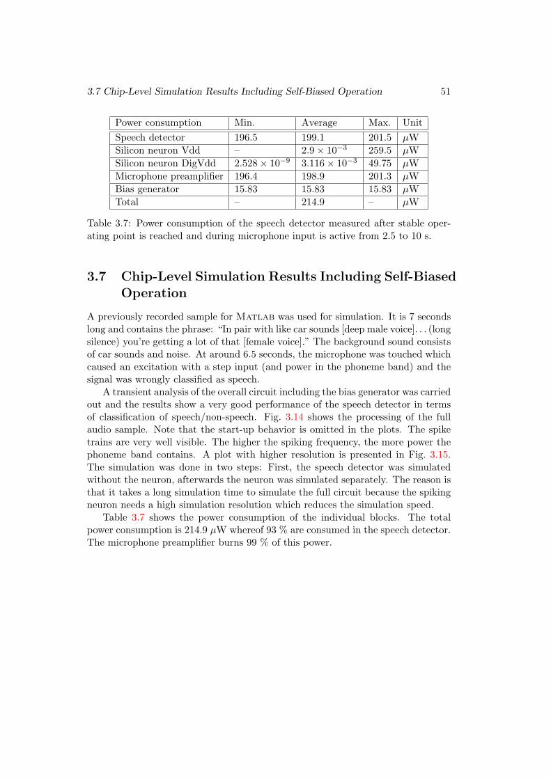
3.7 Chip-Level Simulation Results Including Self-Biased Operation 51
Power consumption Min. Average Max. UnitSpeech detector 196.5 199.1 201.5 µWSilicon neuron Vdd – 2.9× 10⁻³ 259.5 µWSilicon neuron DigVdd 2.528× 10⁻⁹ 3.116× 10⁻³ 49.75 µWMicrophone preamplifier 196.4 198.9 201.3 µWBias generator 15.83 15.83 15.83 µWTotal – 214.9 – µW
Table 3.7: Power consumption of the speech detector measured after stable oper-ating point is reached and during microphone input is active from 2.5 to 10 s.
3.7 Chip-Level Simulation Results Including Self-BiasedOperation
A previously recorded sample for Matlab was used for simulation. It is 7 secondslong and contains the phrase: “In pair with like car sounds [deep male voice]. . . (longsilence) you’re getting a lot of that [female voice].” The background sound consistsof car sounds and noise. At around 6.5 seconds, the microphone was touched whichcaused an excitation with a step input (and power in the phoneme band) and thesignal was wrongly classified as speech.
A transient analysis of the overall circuit including the bias generator was carriedout and the results show a very good performance of the speech detector in termsof classification of speech/non-speech. Fig. 3.14 shows the processing of the fullaudio sample. Note that the start-up behavior is omitted in the plots. The spiketrains are very well visible. The higher the spiking frequency, the more power thephoneme band contains. A plot with higher resolution is presented in Fig. 3.15.The simulation was done in two steps: First, the speech detector was simulatedwithout the neuron, afterwards the neuron was simulated separately. The reason isthat it takes a long simulation time to simulate the full circuit because the spikingneuron needs a high simulation resolution which reduces the simulation speed.
Table 3.7 shows the power consumption of the individual blocks. The totalpower consumption is 214.9 µW whereof 93 % are consumed in the speech detector.The microphone preamplifier burns 99 % of this power.
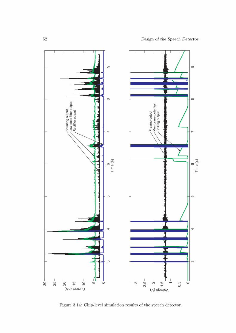
52 Design of the Speech Detector
34
56
78
9051015202530
Tim
e (s
)
Current (nA)
34
56
78
90
0.51
1.52
2.53
Tim
e (s
)
Voltage (V)
Squ
arin
g ou
tput
Low
-pas
s fil
ter o
utpu
tR
ectif
ier o
utpu
t
Pre
amp
outp
utM
embr
ane
pote
ntia
lS
piki
ng o
utpu
t
Figure 3.14: Chip-level simulation results of the speech detector.

3.7 Chip-Level Simulation Results Including Self-Biased Operation 53
3.2
3.21
3.22
3.23
3.24
3.25
3.26
3.27
3.28
3.29
3.3
051015202530
Tim
e (s
)
Current (nA)
3.2
3.21
3.22
3.23
3.24
3.25
3.26
3.27
3.28
3.29
3.3
0
0.51
1.52
2.53
Tim
e (s
)
Voltage (V)
Squ
arin
g ou
tput
Low
-pas
s fil
ter o
utpu
tR
ectif
ier o
utpu
t
Pre
amp
outp
utM
embr
ane
pote
ntia
lS
piki
ng o
utpu
t
Figure 3.15: Chip-level simulation results of the speech detector (high resolution).

54 Design of the Speech Detector

Chapter 4
Layout of the Speech Detector
In this chapter we give an overview of the layout of the speech detector. Layouttechniques as well as EDA related issues are treated. A pin map is included to easephysical characterization of the prototype silicon.
4.1 General Issues
The chip was laid out and will be fabricated in the MOSIS 1.6 µm process (SCGAtechnology) which aims at a 5 V power supply. However, the speech detector cir-cuitry was designed to work at 3.3 V only (Table 4.1).
A summary of project-specific guidelines which had to be respected is as follows:
• A metal2 shield is used which is the ground layer at the same time. We decidedto use a metal shield because photodiodes will be incorporated into the circuitlater on when the face and speech detection circuits will be combined. It isnot necessary for the sake of the speech detector to work properly.
• The power supply line Vdd was given the highest priority, i.e. all other wireshad to circumvent the Vdd wire by poly jumpers that were made 5 poly con-tacts (pcons) wide at maximum. Metal2 could not be used for that purpose asit forms the metal2 Gnd shield. Vdd carries high currents which would cause avoltage drop in the resistive poly layer. Correct circuit functionality could notbe guaranteed. It does not matter for the bias voltages of the gate because
ParameterProcess MOSIS 1.6 µm (SCGA technology)Power supply typ. 3.3 V, max. 5 VLayers 2 metal, 2 poly
Table 4.1: Process characteristics.

56 Layout of the Speech Detector
there are no currents once the gate has been charged. However, coupling ofnoise through the high-impedance node can alter the gate voltages.
• DigVdd and DigGnd lines were given the second priority.
• Gnd contacts were connected to the metal2 shield directly by means of vias,so hardly any Gnd wires can be found in the layout.
• Guard rings: 30λ (λ = 0.8 µm) wide n-well guard rings surrounds the speechdetector as well as the bias generator and are connected to Vdd. They absorbphoto-generated minority carriers.
• A fixed cell height was chosen (where possible) to ease connections to the Vddpower supply bus.
• A wide Vdd bus is placed above the speech detector to contact the Vdd of allcells.
The layout methodology is important to ensure good device matching and cir-cuit operation. This way, undesirable parasitic effects and coupling effects areminimized. Consequently, the physical characteristics will accord more closely withprediction from simulations. This is fundamental for the design of the speech de-tector where several arithmetic computations are successively carried out.
General considerations (partially taken from [11] (pp. 346–352) and [21]):
• Devices are placed in the same orientation to be subjected to the same pro-cessing variations. For example, the current propagation should be in thesame direction.
• Common-centroid structures were used where practical (OpAmp, antibumpcircuit). A common symmetry center for matched devices was arranged touniformly distribute the influences of gradients. However, the total area re-quired is mainly increased due to additional routing.
• Dummy segments are placed on the ends of transistor arrays. The surroundingcircuitry should be similar. Dummy transistors were connected in such a waythat they do not draw current.
• Metal1 is not routed across the active gate area unless there is no otherworkaround because there have been reports that metal crossing channelsincreases mismatch.
• If the active area of a current mirror (e.g. in an OTA) needs to be crossedit should be done in an equal and symmetrical way, thus avoiding differentialcoupling effects.
• Multiple contacts are used to connect two different layers in order to reduceinterlayer resistance (contact resistance Rvia = 0.06 Ω, Rpoly = 27.5 Ω).

4.2 Microphone Preamplifier 57
• To avoid problems such as latch-up and substrate coupling, the potential ofthe substrate and wells has to be properly set by contact rings.
• The capacitors were made of a bottom poly1 plate and a top poly2 plate withthe interpoly oxide as the insulator (sheet resistance R2 = 573 aF/µm2).Quadratic unit capacitor cells were used for a good matching of the filtertime constants.
• Devices to be matched (e.g. transistors in differential pair, current mirrortransistors) are placed close to one another because of the spatial variationsof the process parameters.
• The power supplies of analog and digital circuits are separated. The switchingof a digital signal can couple into an analog circuit and affect its operation.
4.2 Microphone Preamplifier
A common-centroid and compact solution was used for the layout of the differentialpair of the OpAmp because matching is important not to cause systematic offsets.For the same reason, shorted dummy transistors were placed around the currentmirrors in both types of OTAs in order to establish equal surroundings. To ensuregood matching, the transistors of the differential pair and the current mirror areplaced as close to one another as the design rules allow.
4.3 Squaring Circuit
Again, a common-centroid geometry was used for the layout of the antibump circuit(see Figs. 4.1 and 4.2). Since matched devices should have the same surroundings,dummy transistors were put on the edges of the common-centroid structure.
4.4 Silicon Neuron
The branches which carry high switching currents are connected to digital ground(DigGnd) and digital Vdd (DigVdd), respectively. The n-wells of the relevantpFETs are tied to DigVdd, too. Gnd and DigGnd as well as Vdd and DigVddare separate voltage nets in the layout. However, PadGnd and Gnd are shortedwhereas PadVdd is led to a pad and remains unconnected.
4.5 Padframe
The pad assignment was done according to the arrangement of the DollBrain (facedetector) board to reuse the same PCB. However, since 16 pads (14 pads available)are needed to control the bias or reference voltages with the bias DAC, two outputs

58 Layout of the Speech Detector
bM1 G
Dum
my
tQbM2tGtM2bQtM1bbM1tQbM2tGtM2bQtM1bG
Dum
my
bM1 G
Dum
my
tQbM2tGtM2bQtM1bbM1tQbM2tGtM2bQtM1bG
Dum
my
G
G
(a)
(b)
M1 M2
t
tb
b
Q
Dummy
M = 4
M = 8
M = 8
M = 8
M = 8G
Figure 4.1: (a) Schematic of the middle leg of the antibump circuit. M denotesthe number of parallel transistors. (b) Schematic view of the common-centroidstructure as used in the antibump circuit. The dotted lines indicate the axes ofsymmetry. The boxes represent gate fingers.
Figure 4.2: Layout of the antibump circuit. The common-centroid arrangement ofthe transistors of the middle leg is shown.

4.5 Padframe 59
Figure 4.3: Padframe of the speech detector.
(pin no. 18 and 24) to the micro controller are used. 10 pads which lead to thepin header are required (9 pads available). Once again, a microcontroller output isused (pin no. 3). Fig. 4.3 shows an overview of the padframe.
The pad n bias (follbias) supplies the bias voltages for the widepad unity-gainvoltage buffers and is usually about 0.7 V. This bias voltage is not generated bythe on-chip bias generator because it is only meant for debugging. It is not neededfor a functionally correct working chip. If a pad is unused an input pad (inorpad)with electro-static discharge (ESD) protection is used.
4.5.1 Pin Description
All bias voltages are connected to the DAC which is capable of generating therequired gate voltages in case the bias generator has to be overridden. Table 4.2gives an overview of the pin map. The pin number, the signal name, the type of pad,the function and the board connection are listed along with the external wiring withdiscrete elements such as resistors. We decided to use an off-chip feedback resistorRf in order to have more tolerance for debugging.

60 Layout of the Speech Detector
Pin no. Name Pad type Board connection Ext. connection1 preampIn barepad PH JP4/2 Mic and Rs to Gnd2 VRefPreamp barepad DAC3 Vdpfet barepad PH (former µC)4 unused inorpad µC5 n bias barepad DAC6 unused inorpad µCLS7 unused inorpad µC8 unused inorpad µC9 VSquaringOut widepad PH JP4/410 VLowpassOut widepad PH JP4/511 unused inorpad µC12 unused inorpad µC13 unused inorpad µC14 VSNeuron outpad µC, PH JP4/615 PadGnd barepad16 VRectifierOut widepad PH JP4/717 VMNeuron widepad PH JP4/818 VgRectifier barepad DAC (former µC)19 DigGnd barepad PH JP4/920 VRefNeuron barepad DAC21 VThrNeuron barepad DAC22 VCascNeuron barepad DAC23 Ib1Lowpass barepad DAC24 IbOTAPreamp barepad DAC (former µC)25 Vdd barepad26 IbOTASquaring barepad DAC27 IbSquaring barepad DAC28 Ib1OpAmpPreamp barepad DAC29 Ib2OpAmpPreamp barepad DAC30 VLeakNeuron barepad DAC31 IbHighpass barepad DAC32 Ib2Lowpass barepad DAC33 IbOTARectifier barepad DAC34 powerDown inorpad µCLS to Gnd35 PadVdd barepad36 rx barepad RX = 120 kΩ37 BiasGenNBias barepad 10 pF to Gnd38 DigVdd barepad39 Vdnfet barepad PH JP4/340 preampOut barepad PH JP4/1 Rf = 300 kΩ to pin 1
Table 4.2: Pin assignment of the speech detector chip. Notation: µC = microcon-troller, µCLS = microcontroller (level shifter), PH = pin header.

4.6 Bias Generator 61
Area λ unit mm2 unitSpeech detector 1725λ× 480λ 0.828 mm2
Bias generator 1913λ× 587λ 1.123 mm2
Total 1.951 mm2
Table 4.3: Area consumption of the speech detector (λ = 0.8 µm). The arearequired for routing between the speech detector and the bias generator and to thepads is not considered.
4.6 Bias Generator
The layout cell of the bias generator was automatically generated by a compiler [20]but for a slightly different technology. It was deliberately designed for a processwith n- and p-select masks to make the layout portable. Before linking it to thespeech detector, the parameter lambda per internal unit had to be rescaled from1:200 to 1:1000. When the bias generator is linked to the speech detector, the layersmust be mapped accordingly. However, the p-select layer was inherited but is notextracted for fabrication. Since the compiled bias generator was too wide, causedby the difference of bias current of several magnitudes, the master bias block andthe rest of the bias generator circuit had to be split and were stacked on top of eachother (see Fig. 4.4).
Moreover, a test structure consisting of a nFET and a pFET (W/L = 24λ/6λ)was included in the bias generator cell. The structure was placed in the vicinity ofthe master bias to take process variations into account and were covered by metal2to make it insensitive to illumination. The common gate voltage and drain voltagesof the transistors were brought off-chip to measure the individual bias currentsduring debugging. This circuitry allows to probe every bias current provided by thebias generator by connecting the bias voltage pad to the gate of the test transistors.
4.7 Design Rules
Active contacts must be surrounded by 1λ of select. To be on the safe side 2λ werechosen. This rule was not observed by the design-rule checker (DRC).
4.8 Layout Versus Schematic (LVS)
The layout speech detector was verified by a bottom-up approach. The layout ofthe chip is shown in Fig. 4.4. Table 4.3 gives an overview of the required chip area.It is almost ready for tape-out.

62 Layout of the Speech Detector
Figure 4.4: Chip layout.

Appendix A
Analysis of the TransferFunction of the MicrophonePreamplifier
In this chapter we derive the transfer function of the microphone preamplifier ingreat detail. We discuss qualitatively the relevant poles, which are obtained inthe analysis and determine the pass-band of the circuit, and indentify the circuitelements causing the poles.
A.1 Derivation of the Transfer Function
Until now, we have assumed that parasitic capacitances and output resistances arenegligible (refer to Subsection 3.1.4 in Chapter 3). In practice, however, the para-sitic capacitances have a significant effect on bandwidth. To recalculate the transferfunction, the capacitances Cgs1, Cgd1, Cgd2 and the output resistances ro1, ro2 areadded to the circuit as shown in Fig. A.1.
To find a relationship between the equivalent microphone input voltage vi andthe output voltage of the microphone preamplifier vo, Kirchhoff’s current law (KCL)and Kirchhoff’s voltage law (KVL) can be applied at the nodes v1, v2, v3 and aroundthe OpAmp loop, respectively
(vi − v1)sCmic + (v2 − v1)sCgd1 − v1
(1rin
+ sCgs1
)= 0 (A.1)
(v1 − v2)sCgd1 − gm1v1 − gm2v3 + (v3 − v2)sCgd2 +vo − v2
Rf− v2
ro= 0 (A.2)
−v3sCad,tot −v3
Ro+Gm(v2 − vo) + (v2 − v3)sCgd2 = 0 (A.3)
vo +A(s) · v2 = 0 (A.4)
where ro = ro1 ‖ ro2 is the output resistance of the JFET and the pFET of theadaptive element in parallel. This is a set of linear equations with four indepen-

64 Analysis of the Transfer Function of the Microphone Preamplifier
Cmic
rin Cgs1 gm1v1 ro1
Cgd1
vi
+
-
v1
vo=-A(s)v2
Rf
v2
Ro Gm(v2-vo)ro2 gm2v3
Cgd2
Cad,tot
v3Req2
Req1
+
-
Figure A.1: Small-signal equivalent circuit for the microphone preamplifier.
dent variables. Note that the effective capacitance of the adaptive element Cad,tot
comprises of the capacitance of the adaptive element Cad itself, the gate-to-sourcecapacitance Cgs2 and the gate-to-bulk capacitance Cgb2 of the pFET of the adaptiveelement
Cad,tot = Cad + Cgs2 + Cgb2 (A.5)
Solving Eq. (A.4) for v2 gives
v2 = − voA(s)
(A.6)
Substituting Eq. (A.6) into Eq. (A.1) and solving for v1 yields
v1
(s(Cmic + Cgd1 + Cgs1) +
1rin
)= vi · sCmic −
voAsCgd1 (A.7)
⇒ v1 =vi · sCmic − vo
A sCgd1
s(Cmic + Cgd1 + Cgs1) + 1rin
(A.8)
Solving for Eq. (A.3) for v3 gives
v3
(sCad,tot +
1Ro
+ sCgd2
)= −Gmvo
(1 +
1A(s)
)− voA(s)
sCgd2 (A.9)
⇒ v3 = vo−Gm
(1 + 1
A(s)
)− sCgd2
A(s)
s(Cad,tot + Cgd2) + 1Ro
(A.10)

A.1 Derivation of the Transfer Function 65
Rearranging Eq. (A.2) for the voltages gives
v1(sCgd1 − gm1) + v2
(−s(Cgd1 + Cgd2)− 1
Rf− 1ro
)+ v3(−gm2 + sCgd2) +
voRf
= 0
(A.11)
Substitution of Eq. (A.6) in Eq. (A.11) yields
v1(sCgd1 − gm1) + v3(−gm2 + sCgd2) + vo
(1Rf
+s(Cgd1 + Cgd2) + 1
Rf+ 1
ro
A(s)
)= 0
(A.12)
Substituting Eqs. (A.8) and (A.10) into the preceding equation gives
visCmic(sCgd1 − gm1)
s(Cmic + Cgd + Cgs) + 1rin
+ vo
−Gm(
1 + 1A(s)
)− sCgd2
A(s)
sCad,tot + 1Ro
+ sCgd2
(−gm2 + sCgd2) . . .
. . . −sCgd1A (sCgd1 − gm1)
s(Cmic + Cgd1 + Cgs1) + 1rin
+1Rf
+s(Cgd1 + Cgd2) + 1
Rf+ 1
ro
A(s)
)= 0
(A.13)
The transfer function of the circuit in the Laplace domain is given by
H(s) =vovi
=−sCmic(sCgd1 − gm1)(
s(Cmic + Cgd1 + Cgs1) + 1rin
)·
(−Gm
“1+ 1
A(s)
”−sCgd2A(s)
s(Cad,tot+Cgd2)+ 1Ro
(−gm2 + sCgd2) . . .
. . . − sCgd1A(s)(sCgd−gm1)
s(Cmic+Cgd1+Cgs1)+ 1rin
+ 1Rf
+s(Cgd1+Cgd2)+ 1
Rf+ 1ro
A(s)
)(A.14)
Simulations with Matlab have shown (see Fig. A.5) that in the frequency rangeof interest and for the circuit parameters extracted from T-Spice the denominatorcan be simplified to
H(s) =−sCmic(sCgd1 − gm1)(
s(Cmic + Cgd1 + Cgs1) + 1rin
)·
(−Gm
“1+ 1
A(s)
”−sCgd2A(s)
s(Cad,tot+Cgd2)+ 1Ro
(−gm2 + sCgd2) + 1Rf
)(A.15)
Substituting the gain function of the OpAmp which contains a single pole fromEq. (3.6) in Subsection 3.1.1 of Chapter 3
A(s) =ADC,OA
1− spOA
=ADC,OA
1 + s · τp,OA(A.16)

66 Analysis of the Transfer Function of the Microphone Preamplifier
into the second term of the denominator of Eq. (A.15)
T (s) =(−Gm
ADC,OA + 1ADC,OA
(1 +
τp,OA
τp,OA + 1
)−
sCgd2
ADC,OA(1 + sτp,OA)
)· · ·
· · · (−gm2 + sCgd2) +s(Cad,tot + Cgd2)
Rf+
1RoRf
(A.17)
Simplifying and rearranging gives
T (s) ≈(Gm +
s2Cgd2τp,OA
ADC,OA
)gm2 +
s(Cad,tot + Cgd2)Rf
(A.18)
= s2Cgd2τp,OAgm2
ADC,OA+ s
Cad,tot + Cgd2
Rf+ gm2Gm (A.19)
= gm2Gm
(s2 Cgd2τp,OA
ADC,OAGm+ s
Cad,tot + Cgd2
Rfgm2Gm+ 1)
(A.20)
The polynomial T (s) has two poles p2, p3. Assuming that p3 p2, the followingsimplification applies
T (s) = s2a+ sb+ 1 =(
1− s
p2
)(1− s
p3
)= s2 1
p2p3− s
(1p2
+1p3
)+ 1 (A.21)
p3p2≈ s2 1p2p3
− s 1p2
+ 1 (A.22)
Thus, the poles are given by
p2 = −1b
= −Rfgm2Gm
Cad,tot + Cgd2(A.23)
p3 = − ba
= −ADC,OA(Cad,tot + Cgd2)
Cgd2τp,OAgm2Rf(A.24)
The transfer function in the Laplace domain from the equivalent microphoneinput voltage vi to the microphone preamplifier output vo is
H(s) =gm1Cmicrin
gm2GmRo
s(s(Cad,tot + Cgd2)Ro + 1
) (1− sCgdgm1
)(1 + s(Cmic + Cgd1 + Cgs1)rin
) (1 + s
Cad,tot+Cgd2Rfgm2Gm
)· · ·
· · ·(
1 + sCgd2τp,OAgm2RfADC,OA(Cad+Cgd2)
)=gm1Cmicrin
gm2GmRo
s(
1− sz2
)(1 + s
z3
)(
1− sp1
)(1− s
p2
)(1− s
p3
)(A.25)
A.1 Derivation of the Transfer Function 67
where
z1 = 0 (A.26)
z2 =1
(Cad,tot + Cgd2)Ro(A.27)
z3 =gm1
Cgd(A.28)
p1 = − 1(Cmic + Cgd1 + Cgs1)rin
(A.29)
p2 = −Rfgm2Gm
Cad,tot + Cgd2(A.30)
p3 = −ADC,OA(Cad,tot + Cgd2)
τp,OACgd2gm2Rf= −
GBPOA(Cad,tot + Cgd2)Cgd2gm2Rf
(A.31)
where GBPOA is the gain-bandwidth product of the OpAmp. Because the transferfunction contains both three zeros and three poles and a term causing a high-frequency pole was neglected in Eq. (A.14), the magnitude of the frequency responseis flat for high frequencies. Otherwise the system would roll off for infinitely highfrequencies.
The pass-band (or in-band) gain is found to be
HPB =gm1Cmicrin
gm2GmRo
|p1| · |p2|z2
= gm1RfCmic
Cmic + Cgd1 + Cgs1(A.32)
The gain-bandwidth product GBP of the microphone preamplifier circuit is givenby
GBP = HPB · |p3| =ADC,OA(Cad,tot + Cgd2)gm1Cmic
τp,OACgd2gm2(Cmic + Cgd1 + Cgs1)(A.33)
=GBPOA(Cad,tot + Cgd2)gm1Cmic
Cgd2gm2(Cmic + Cgd1 + Cgs1)(A.34)
A.1.1 Numerical Calculations
The parameters of the circuit elements are extracted from T-Spice and are listedin Table A.1.
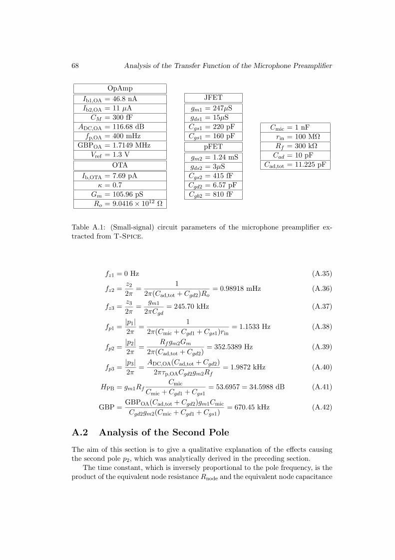
68 Analysis of the Transfer Function of the Microphone Preamplifier
OpAmpIb1,OA = 46.8 nAIb2,OA = 11 µACM = 300 fF
ADC,OA = 116.68 dBfp,OA = 400 mHz
GBPOA = 1.7149 MHzVref = 1.3 V
OTAIb,OTA = 7.69 pA
κ = 0.7Gm = 105.96 pSRo = 9.0416× 10¹² Ω
JFETgm1 = 247µSgds1 = 15µSCgs1 = 220 pFCgs1 = 160 pF
pFETgm2 = 1.24 mSgds2 = 3µSCgs2 = 415 fFCgd2 = 6.57 pFCgb2 = 810 fF
Cmic = 1 nFrin = 100 MΩRf = 300 kΩCad = 10 pF
Cad,tot = 11.225 pF
Table A.1: (Small-signal) circuit parameters of the microphone preamplifier ex-tracted from T-Spice.
fz1 = 0 Hz (A.35)
fz2 =z2
2π=
12π(Cad,tot + Cgd2)Ro
= 0.98918 mHz (A.36)
fz3 =z3
2π=
gm1
2πCgd= 245.70 kHz (A.37)
fp1 =|p1|2π
=1
2π(Cmic + Cgd1 + Cgs1)rin= 1.1533 Hz (A.38)
fp2 =|p2|2π
=Rfgm2Gm
2π(Cad,tot + Cgd2)= 352.5389 Hz (A.39)
fp3 =|p3|2π
=ADC,OA(Cad,tot + Cgd2)
2πτp,OACgd2gm2Rf= 1.9872 kHz (A.40)
HPB = gm1RfCmic
Cmic + Cgd1 + Cgs1= 53.6957 = 34.5988 dB (A.41)
GBP =GBPOA(Cad,tot + Cgd2)gm1Cmic
Cgd2gm2(Cmic + Cgd1 + Cgs1)= 670.45 kHz (A.42)
A.2 Analysis of the Second Pole
The aim of this section is to give a qualitative explanation of the effects causingthe second pole p2, which was analytically derived in the preceding section.
The time constant, which is inversely proportional to the pole frequency, is theproduct of the equivalent node resistance Rnode and the equivalent node capacitance

A.2 Analysis of the Second Pole 69
vo=-A(s)v2
Rf
v2
Ro Gm(v2-vo)ro2 gm2v3
Cgd2
Cad,tot
v3
+
-
vt
+
-
it
Figure A.2: Circuit for the calculation of the node resistance and capacitance ofthe adaptive element.
Cnode
τnode = Rnode · Cnode (A.43)
The equivalent node resistance of node v3 can be found by applying a testvoltage source vt at node v3 and measuring the test current without consideringthe capacitive effects as shown in Fig. A.2. This way the feedback loop is takeninto account. The ratio vt/it is equal to the equivalent resistance Req. Applyinga test voltage vt creates a small-signal current through the pFET which is equalto gm2 · vt. This current is amplified across the feedback resistor Rf and turnedinto a voltage vRf = Rfgm2 · vt. The voltage drop across the resistor is sensed bythe OTA and converted into the final small-signal test current it = GmRfgm2 · vt.Therefore, the associated resistance is given by
Req =vtit
=1
GmRfgm2(A.44)
The total node resistance is given by the equivalent resistance in parallel with theoutput resistance of the OTA, which simplifies to Req because Req is much smallerthan Ro
Rnode = Req ‖ RoReqRo≈ Req =
1GmRfgm2
(A.45)
Here, the elements of the microphone model are not considered for simplicity.Assuming that the OpAmp has infinite gain and is infinitely fast, it clamps theinput of the OpAmp v2 approximately at virtual ground. The associated nodecapacitance Cnode is the capacitance of the adaptive element Cad,tot in parallel withthe parasitic gate-to-drain capacitance Cgd2 of the pFET
Cnode = Cad,tot + Cgd2 (A.46)

70 Analysis of the Transfer Function of the Microphone Preamplifier
AOA(s)+
-
f
vi
vo
vfb
vε
Figure A.3: Operational amplifier in feedback configuration.
Hence, the associated time constant of node v3 is given by
τnode = RnodeCnode =Cad + Cgd2
GmRfgm2(A.47)
and the pole is given by
p2 =1
τnode=
GmRfgm2
Cad + Cgd2(A.48)
Thus, the results of the foregoing section are qualitatively explained and confirmed.
A.3 Analysis of the Third Pole
To explain the effects causing the third pole, the influence of feedback on bandwidthneeds to be discussed based on [22] (pp. 624–625).
A.3.1 Relation Between Gain and Bandwidth in Feedback Ampli-fiers
Consider first an OpAmp in feedback configuration as shown in Fig. A.3 with asimple basic amplifier whose gain function contains a single pole
AOA(s) =ADC,OA
1− spOA
=ADC,OA
1 + s · τp,OA(A.49)
where ADC,OA is the low-frequency gain of the OpAmp and pOA and τp,OA are thepole and the time constant, respectively. The feedback configuration minimizes theerror signal vε
vε = vi − vfb (A.50)
The output signal of the OpAmp is equal to
vo = AOA(s) · vε (A.51)

A.3 Analysis of the Third Pole 71
where AOA(s) is the open loop gain of the amplifier. The amount of the outputsignal which is fed back to the input of the amplifier is given by
vfb = f · vo (A.52)
where f is the feedback function. The feedback function f is a positive constantif we assume that the feedback path is purely resistive. This assumption is validfor the feedback configuration in the context of the microphone preamplifier. Theoverall gain is
vo = AOA(s) · vε = AOA(s) · (vi − vfb) = AOA(s)(vi − f · vo) (A.53)
⇒ vovi
=AOA(s)
1 +AOA(s) · f=
AOA(s)1 + T (s)
(A.54)
where T (s) = AOA(s) · f is the loop gain. Substitution of Eq. (A.49) in Eq. (A.54)gives
A(s) =
ADC,OA
1− spOA
1 + ADC,OAf1− s
pOA
=ADC,OA
1− spOA
+ADC,OAf(A.55)
=ADC,OA
1 +ADC,OAf
11− s
pOA
11+ADC,OAf
(A.56)
From Eq. (A.56) the low-frequency gain A0 is
A0 =ADC,OA
1 + T0(A.57)
where
T0 = ADC,OAf (A.58)
is the low-frequency loop gain. From Eq. (A.56) the cutoff frequency (i.e. the newpole magnitude) and the time constant of the feedback circuit are
p = (1 +ADC,OAf) · |pOA| =1 +ADC,OAf
τp,OA(A.59)
τ =1
1 +ADC,OAfτp,OA (A.60)
Thus the feedback has reduced the low-frequency gain by a factor (1 + T0) but thecutoff frequency has been increased by the same amount (1 + T0). Note that thegain-bandwidth product (GBP) is constant
GBP = ADC,OA · pOA =ADC,OA
τp,OA(A.61)
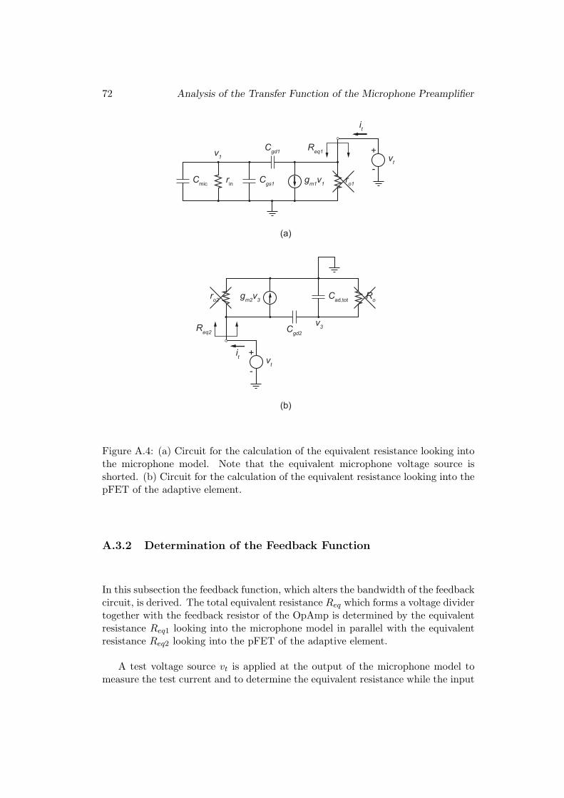
72 Analysis of the Transfer Function of the Microphone Preamplifier
Roro2 gm2v3
Cgd2
Cad,tot
v3Req2
it vt
+
-
rin Cgs1 gm1v1 ro1
Cgd1v1Req1
Cmic
it
vt
+
-
(a)
(b)
Figure A.4: (a) Circuit for the calculation of the equivalent resistance looking intothe microphone model. Note that the equivalent microphone voltage source isshorted. (b) Circuit for the calculation of the equivalent resistance looking into thepFET of the adaptive element.
A.3.2 Determination of the Feedback Function
In this subsection the feedback function, which alters the bandwidth of the feedbackcircuit, is derived. The total equivalent resistance Req which forms a voltage dividertogether with the feedback resistor of the OpAmp is determined by the equivalentresistance Req1 looking into the microphone model in parallel with the equivalentresistance Req2 looking into the pFET of the adaptive element.
A test voltage source vt is applied at the output of the microphone model tomeasure the test current and to determine the equivalent resistance while the input

A.3 Analysis of the Third Pole 73
voltage source vi is shorted as shown in Fig. A.4 (a)
v1 =
1s(Cmic+Cgs1)+ 1
rin
1sCgd1
+ 1s(Cmic+Cgs1)+ 1
rin
vt =sCgd1
s(Cmic + Cgs1 + Cgd1) + 1rin
vt (A.62)
≈Cgd1
Cmic + Cgs1 + Cgd1vt =
1
1 + Cmic+Cgs1Cgd1
≈ 18vt (A.63)
In both analyses the output resistances of the pFET and JFET are neglected be-cause they are much higher. Moreover, the currents through the capacitive dividersare not considered. The input test current is
it ≈ gm1v1 =gm1
1 + Cmic+Cgs1Cgd1
vt (A.64)
The equivalent resistance Req1 is given by
Req1 =vtit
=1 + Cmic+Cgs1
Cgd1
gm1= 34.919 kΩ (A.65)
Similarly, the equivalent resistance looking into the drain of the pFET of theadaptive element can be determined (see Fig. A.4 (b))
it = gm2Cgd2
Cad,tot + Cgd2vt +
sCad,totCgd2
Cad + Cgd2vt (A.66)
≈ gm2Cgd2
Cad,tot + Cgd2vt (A.67)
The equivalent resistance Req2 is
Req2 =vtit
=Cad,tot + Cgd2
gm2Cgd2= 2.1843 kΩ (A.68)
which is much smaller by a factor of 15 than the input resistance seen looking intothe pFET and the adaptive element. We assume that feedback through the OTAhas no effect because it forms a low-pass filter and high frequencies are attenuated.Therefore, the total resistance is found to be
Req = Req1 ‖ Req2Req1Req2≈ Req2 (A.69)
The voltage divider rule from the output of the OpAmp v0 to the invertinginput v2 yields
v2 =Req
Req +Rfv0
RfReq≈ Req
Rfv0 =
Cad,tot + Cgd2
Cgd2gm2Rfvo (A.70)

74 Analysis of the Transfer Function of the Microphone Preamplifier
The feedback function is given by
f =v2
v0=Cgd2 + Cad,tot
Cgd2gm2Rf(A.71)
From Eq. (A.59) the magnitude of the pole is
|p3| = (1 +ADC,OAf) · pOA
ADC,OAf1≈ ADC,OAf · pOA =
ADC,OAf
τp,OA(A.72)
=ADC,OA(Cad,tot + Cgd2)
τp,OACgd2gm2Rf=
GBPOA(Cad,tot + Cgd2)Cgd2gm2Rf
(A.73)
which is in accordance with the results obtained in Section A.1. It is apparent thatthe magnitude of the third pole |p3| is proportional to the gain-bandwidth productof the OpAmp GBPOA and inversely proportional to the capacitive divider ratio.
A.4 Discussion of the Results
It is shown that the pole causing the rolloff in the transfer function of the micro-phone preamplifier is caused by capacitive coupling from the OpAmp onto the gateof the pFET through Cgd2 and that the bandwidth is drastically reduced.
Theoretically, the gain-bandwidth product of the OpAmp GBPOA can be re-duced to move the third pole to lower frequencies by decreasing the bias current ofthe output stage of the OpAmp. However, this current cannot be further reduced inthe present design because the bias current should be capable of delivering at leastthe maximum signal current of the microphone in the order of 10 µA. Otherwisethe OpAmp slews and the signal is clipped.
Alternatively, the frequency of the third pole can be lowered by making thepFET of the adaptive element M2 wider which in turn increases its parasitic gate-to-drain capacitance Cgd2 or by deliberately connecting a capacitor between thegate and the drain of the pFET to increase the effective gate-to-drain capacitance.
For the simplified analysis in Subsection 3.1.4 of Chapter 3, the feedback func-tion f was equal to 1 because the parasitic capacitances and output resistancesof the pFET and the JFET were not considered and the equivalent resistanceReq →∞.
f =Req
Req +Rf
Req→∞→ 1 (A.74)
Therefore, the bandwidth of the circuit was maximum.

A.4 Discussion of the Results 75
10-1 100 101 102 103 104 105 106-60
-40
-20
0
20
40
Frequency (Hz)
Mag
nitu
de (d
B)
10-1 100 101 102 103 104 105 106-200
-150
-100
-50
0
50
100
150
200
Frequency (Hz)
Pha
se (d
eg)
Simulation data
Ideal form
Simplified form
Simulation dataSimplified form
Ideal form
Figure A.5: Transfer function of the microphone preamplifier including the micro-phone model from the microphone equivalent voltage source to the preamplifieroutput voltage. The ideal form includes the terms which are neglected in order toderive the poles determining the pass-band. It is apparent that the terms influ-ence the frequency response only for high frequencies and that the approximationis appropriate for the derivation of the poles p2 and p3.

76 Analysis of the Transfer Function of the Microphone Preamplifier

Appendix B
Details Required for ChipTesting
Cochlea subversion base URL:https://svn.ini.unizh.ch/repos/avlsi/common/projects/cochleaAMSBiasgenPreamp(password protected)
Dollbrain project subversion base URL:https://svn.ini.uzh.ch/repos/avlsi/db (password protected)

78 Details Required for Chip Testing

Bibliography
[1] DollBrain project: Micropower integrated face and voice detection. Available:http://dollbrain.ini.uzh.ch.
[2] M. C. Buchler. Algorithms for Sound Classification in Hearing Instruments.Diss. ETH no 14498, 2002.
[3] M. W. Baker and R. Sarpeshkar. “A low-power high-PSRR current-modemicrophone preamplifier,” IEEE Journal of Solid-State Circuits, Vol. 38, Issue10, pp. 1671–1678, October 2003.
[4] HandiWorks web page. Available: http://www.handiworks.com/pd_find.cfm.
[5] K. Heutschi. Skript Akustik II (227-0478-00). Institut fur Signal- und Infor-mationsverarbeitung, ETHZ, June 2006.
[6] J. Eargle. The microphone book. Elsevier, Amsterdam, 2004.
[7] G. M. Sessler. “Electrostatic Microphones with Electret Foil,” The Journal ofthe Acoustical Society of America, Vol. 35, Number 9, pp. 1354–1357, Septem-ber 1963.
[8] A. van Rhijn. “Integrated Circuits for High Performance Electret Micro-phones,” Audio Engineering Society Convention Paper, Amsterdam, March2003.
[9] Unpublished. Tanner EDA T-Spice 12 User Guide.
[10] Knowles Acoustics MD9745APA-1 data sheet. Available: http://www.farnell.com/datasheets/87224.pdf.
[11] S.-C. Liu, J. Kramer, G. Indivieri, T. Delbruck, and R. Douglas. Analog VLSI:Circuits and Principles. MIT Press, Cambridge, November 2002.
[12] T. Delbruck. ““Bump” circuits for computing similarity and dissimilarity ofanalog voltages,” Proceedings of International Joint Conference on NeuralNetworks, Seattle Washington, pp. I–475–479, July 1991.
80 BIBLIOGRAPHY
[13] T. Delbruck and D. Oberhof. “Self biased low power adaptive photorecep-tor”, 2004 International Symposium on Circuits and Systems (ISCAS 2004),Vancouver, pp. IV–844–847, May 2004.
[14] J. Mulder, W. A. Serdijn, A. C. Van der Woerd, and A. H. M. van Roer-mund. Dynamic Translinear and Log-Domain Circuits: Analysis and Synthe-sis. Kluwer, Boston, 1998.
[15] T. Delbruck and C. A. Mead. “Analog VLSI phototransduction by continuous-time, adaptive, logarithmic photoreceptor circuits,” Vision Chips: Implement-ing vision algorithms with analog VLSI circuits, C. Koch and H. Li editors,IEEE Computer Society Press, pp. 139–161, 1995.
[16] S. M. Zhak, M. W. Baker, and R. Sarpeshkar. “A low-power wide dynamicrange envelope detector,” IEEE Journal of Solid-State Circuits, Vol. 38, Issue10, pp. 1750–1753, October 2003.
[17] M. Baker, S. Zhak, and R. Sarpheshkar. “A micropower envelope detectorfor audio applications,” Proceedings of the 2003 International Symposium onCircuits and Systems (ISCAS 2003), Vol. 5, pp. V–1–4, May 2003.
[18] G. Indiveri, E. Chicca, and R. Douglas. “A VLSI array of low-power spikingneurons and bistable synapses with spiketiming dependent plasticity,” IEEETransactions on Neural Networks, Vol. 17, Issue 1, pp. 211–221, January 2006.
[19] D. D. Ben Dayan Rubin, E. Chicca, and G. Indiveri. “Characterizing the firingproprieties of an adaptive analog VLSI neuron,” Lecture Notes in ComputerScience, 3141, pp. 189–200, 2004.
[20] T. Delbruck and A. van Schaik. “Bias current generators with wide dynamicrange,” Analog Integrated Circuits and Signal Processing, Vol. 43, pp. 247–268,2005.
[21] Unpublished. Maher Kayal. EDATP Addendum: Guidelines to do an AnalogLayout, Analog IC Design Course, EPFL, 2007.
[22] P. R. Gray, P. J. Hurst, S. H. Lewis, and R. G. Meyer. Analysis and design ofanalog integrated circuits. Fourth edition, Wiley, New York, 2001.