PESD5V0F1BSF - Extremely Low Capacitance Bidirectional ESD Protection Diode - NXP
University of Central Florida University of Central Florida
STARS STARS
Electronic Theses and Dissertations
2018
Design of Low-Capacitance Electrostatic Discharge (ESD) Design of Low-Capacitance Electrostatic Discharge (ESD)
Protection Devices in Advanced Silicon Technologies. Protection Devices in Advanced Silicon Technologies.
Aihua Dong University of Central Florida
Part of the Electrical and Electronics Commons
Find similar works at: https://stars.library.ucf.edu/etd
University of Central Florida Libraries http://library.ucf.edu
This Doctoral Dissertation (Open Access) is brought to you for free and open access by STARS. It has been accepted
for inclusion in Electronic Theses and Dissertations by an authorized administrator of STARS. For more information,
please contact [email protected].
STARS Citation STARS Citation Dong, Aihua, "Design of Low-Capacitance Electrostatic Discharge (ESD) Protection Devices in Advanced Silicon Technologies." (2018). Electronic Theses and Dissertations. 5992. https://stars.library.ucf.edu/etd/5992

DESIGN OF LOW-CAPACITANCE ELECTROSTATIC DISCHARGE (ESD)
PROTECTION DEVICES IN ADVANCED SILICON TECHNOLOGIES
by
AIHUA DONG
B.S. University of Electronic Science and Technology of China, 2013
M.S. University of Central Florida, 2016
A dissertation submitted in partial fulfillment of the requirements
for the degree of Doctor of Philosophy
in the Department of Electrical and Computer Engineering
in the College of Engineering and Computer Science
at the University of Central Florida
Orlando, Florida
Summer Term
2018
Major Professor
Kalpathy B. Sundaram

ii
© 2018 Aihua Dong
iii
ABSTRACT
Electrostatic discharge (ESD) related failure is a major IC reliability concern and this is
particularly true as technology continues shrink to nano-metric dimensions. ESD design window
research shows that ESD robustness of victim devices keep decreasing from 350nm bulk
technology to 7nm FinFET technologies. In the meantime, parasitic capacitance of ESD diode
with same It2 in FinFET technologies is approximately 3X compared with that in planar
technologies. Thus transition from planar to FinFET technology requires more robust ESD
protection however the large parasitic capacitance of ESD protection cell is problematic in high-
speed interface design. To reduce the parasitic capacitance, a dual diode silicon controlled
rectifier (DD-SCR) is presented in this dissertation. This design can exhibit good trade-offs
between ESD robustness and parasitic capacitance characteristics. Besides, different bounding
materials lead to performance variations in DD-SCRs are compared. Radio frequency (RF)
technology is also demanded low capacitance ESD protection. To address this concern, a π-
network is presented, providing robust ESD protection for 10-60 GHz RF circuit. Like a low
pass π filter, the network can reflect high frequency RF signals and transmit low frequency ESD
pulses. Given proper inductor value, networks can work as robust ESD solutions at a certain
Giga Hertz frequency range, making this design suitable for broad band protection in RF
input/outputs (I/Os). To increase the holding voltage and reduce snapback, a resistor assist
triggering heterogeneous stacking structure is presented in this dissertation, which can increase
the holding voltage and also keep the trigger voltage nearly as same as a single SCR device.
Keywords: ESD, low capacitance, high speed, design window, TLP.

iv
To my parents Xilan Liu and Fu Dong
v
ACKNOWLEDGMENTS
The four-year Ph.D experience at UCF is one of the most precious memories in my life. I
met knowledgeable professors, experienced engineers and caring friends who give me great
support for my study, work, and life. I would like to show my greatest appreciation for their
supporting me to pursuit my Ph.D degree and go forward in my research.
Frist, I would like to specially thank Dr. Juin J. Liou for his support and supervision
during my Ph.D. study. Thanks him to establish the ESD lab in UCF, in which I finished most of
my research work during Ph.D time. He always gives me expert suggestions when I encounter
obstacles in my research and helps to keep my research on the right track. Dr. Liou also
encourages me and introduces me to work with industrial ESD professionals. Thanks for his trust,
I got involved in in the funded research projects with Analog Devices Inc. (ADI), in which, I
learned a lot and accomplished several publications which greatly contributed to the completion
of this dissertation.
I want to show my great gratitude to Dr. Kalpathy B. Sundaram (UCF) for for his
generous help and supervision to finish my Ph.D. study. I can’t say enough about what a great
person he is. He is always patient and kind and always give professional advices for my study.
His solid understanding in semiconductor device physics helps me a lot to make this dissertation
better.
I also want to thank the generous help from Dr. Jean-Jacques Hajjar, Dr. Javier Salcedo,
Srivatsan Parthasarathy, Dr. Yuanzhong Zhou, Dr. Sirui Luo and all the ESD team members in
ADI. I have a wonderful time in ADI-UCF project. Dr. Hajjar is an experienced and professional
manager, and he always give me professional advices and guidance on my research works. My

vi
mentor Javier Salcedo and Srivatsan Parthasarathy, they are both professional and productive.
Thanks them to inspire me a lot on my research and their trust to let me implement my ideas.
Also thank them always provide helpful comments and revisions on my paper writing. The
achievements from this project are the foundation of this dissertation.
I also would like to thank my wonderful manager Dr. Robert Gauthier Jr. and my
excellent colleagues for their generous help and supportive guidance during my internship at
GlobalFoundries, including Wei Liang, Da-Hsien Lin, Souvick Mitra, Alain Loiseau, Xuejiao
Yang, Meng Miao, Anindya Nath, You Li, Xiangxiang Lu, Tsung-Che Tsai, Harsh Shah, and etc.
I also want to thank all my doctoral committee members, Dr. Javier Salcedo (ADI), Dr.
Lei Wei (UCF), Dr. Xun Gong (UCF), and Dr. Deliang Fan (UCF), for their time spent for me
and their professional suggestions given to my dissertation.
I also want to special thanks to Sirui Luo (ADI), Zhixin Wang (Apple), Yunfeng Xi
(Silicon Labs), Meng Miao (GF), Wei Liang (GF), Linfeng He (UCF), Hang Li (UCF), for the
valuable time that we spent together in UCF.
Last but not least, I want to show my deeply gratitude to my parents, Xilan Liu and Fu
Dong. Their unconditional love and understanding is my greatest motivation to accomplish this
research work.

vii
TABLE OF CONTENTS
LIST OF FIGURES ........................................................................................................................ x
LIST OF TABLES ........................................................................................................................ xv
LIST OF ACRONYMS ............................................................................................................... xvi
CHAPTER 1 INTRODUCTION ................................................................................................. 1
1.1 ESD Event and Protection Methodology .............................................................. 1
1.2 ESD Models .......................................................................................................... 4
1.2.1 Human Body Model ........................................................................................ 5
1.2.2 Machine Model ............................................................................................... 6
1.2.3 Charged Device Model.................................................................................... 8
1.2.4 ESD Model Comparison ................................................................................. 9
1.2.5 Transmission Line Pulse Tester .................................................................... 10
1.3 ESD Protection Device........................................................................................ 12
1.3.1 Diode ............................................................................................................. 14
1.3.2 GGNMOS...................................................................................................... 15
1.3.3 SCR ............................................................................................................... 17
1.4 ESD Protection Circuit ........................................................................................ 18
1.5 Summary and Dissertation Outline ..................................................................... 21

viii
CHAPTER 2 STUDY OF ESD DESIGN WINDOW SCALING DOWN TO 7NM
TECHNOLOGY NODE ............................................................................................................... 23
2.1 Introduction ......................................................................................................... 23
2.2 Technology Background ..................................................................................... 25
2.3 Trend of Parameters ............................................................................................ 28
2.4 Design Window and ESD Protection Level ........................................................ 37
2.5 Conclusion ........................................................................................................... 40
CHAPTER 3 DUAL-DIODE SCR WITH REDUCED CAPACITANCE AND OVERSHOOT
VALTAGE FOR HIGH SPEED INTERFACE APPLICATIONS .............................................. 41
3.1 Introduction ......................................................................................................... 41
3.2 Device Structure .................................................................................................. 44
3.3 Experimental Result ............................................................................................ 47
3.4 Conclusion ........................................................................................................... 54
CHAPTER 4 A DISTRIBUTED SHUNT π–NETWORK FOR RF I/O ESD PROTECTION 56
4.1 Introduction ......................................................................................................... 56
4.2 Network Structure ............................................................................................... 57
4.3 Experimental Result ............................................................................................ 64
4.4 Conclusion ........................................................................................................... 72
CHAPTER 5 HIGH HOLDING VOLTAGE HETEROGENEOUS STACKING SCR........... 74
5.1 Introduction ......................................................................................................... 74

ix
5.2 Device Structure .................................................................................................. 75
5.3 Experimental Results........................................................................................... 77
5.4 Conclusion ........................................................................................................... 79
CHAPTER 6 SUMMARY AND CONCLUSION .................................................................... 80
LIST OF REFERENCES .............................................................................................................. 82

x
LIST OF FIGURES
Figure 1-1 Drain junction damage induced by ESD stress. ............................................................ 2
Figure 1-2 Metal melt damage by ESD stress. ............................................................................... 2
Figure 1-3 ESD protection design window. .................................................................................... 3
Figure 1-4 A simplified equivalent circuit of HBM. ...................................................................... 5
Figure 1-5 Current waveform of HBM when VHBM = 2KV. .......................................................... 5
Figure 1-6 A simplified equivalent circuit of MM. ........................................................................ 6
Figure 1-7 Current waveform of MM when VMM = 200V. ............................................................ 7
Figure 1-8 A simplified equivalent circuit of CDM. ...................................................................... 8
Figure 1-9 Current waveform of CDM when VCDM = 500V. ......................................................... 8
Figure 1-10 Current waveform comparison of HBM, MM and CDM model. ............................... 9
Figure 1-11 A simplified equivalent circuit of TLP tester. ........................................................... 11
Figure 1-12 TLP tester measures I and V at each voltage pulse. .................................................. 12
Figure 1-13 Cross section view of a P+/NW diode. ..................................................................... 14
Figure 1-14 Cross section view of a series diode. ........................................................................ 14
Figure 1-15 TLP characteristics of diode...................................................................................... 15
Figure 1-16 Equivalent circuit and cross section view with parasite NPN of a GGNMOS. ........ 16
Figure 1-17 Equivalent parasitic capacitance of GGNMOS......................................................... 16
Figure 1-18 Equivalent circuit and cross section view with parasite BJTs of a SCR. .................. 17
Figure 1-19 TLP characteristics of SCR. ...................................................................................... 18
Figure 1-20 Typical ESD protection circuit topology: (a) VDD-based (b) VSS-based protection
schemes. ........................................................................................................................................ 19
xi
Figure 1-21 Double diode ESD protection scheme. ..................................................................... 19
Figure 1-22 GGNMOS ESD protection scheme. .......................................................................... 20
Figure 1-23 SCR ESD protection scheme. ................................................................................... 20
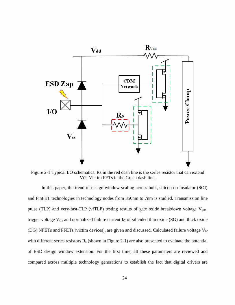
Figure 2-1 Typical I/O schematics. Rs in the red dash line is the series resistor that can extend
Vt2. Victim FETs in the Green dash line. ..................................................................................... 24
Figure 2-2 3-D structure of NFETs in bulk, SOI and FinFET technology. .................................. 25
Figure 2-3 Normalized SG gate oxide thickness in different technologies. Ratio against Tox of
350nm SG NFET. ......................................................................................................................... 27
Figure 2-4 Normalized DG gate oxide thickness in different technologies. Ratio against Tox of
350nm DG NFET. ......................................................................................................................... 27
Figure 2-5100ns TLP gate oxide breakdown voltage of SG NFET in different technologies. .... 28
Figure 2-6 100ns TLP gate oxide breakdown voltage of SG PFET in different technologies. .... 29
Figure 2-7 100ns TLP gate oxide breakdown voltage of DG NFET in different technologies. ... 29
Figure 2-8 100ns TLP trigger voltage of SG NFET in different technologies. ............................ 31
Figure 2-9 100ns TLP trigger voltage of SG PFET in different technologies. ............................. 31
Figure 2-10 100ns TLP trigger voltage of DG NFET in different technologies. ......................... 32
Figure 2-11 1ns TLP normalized It2 of SG NFET in different technologies. ............................... 33
Figure 2-12 1ns TLP normalized It2 of SG PFET in different technologies. ................................ 33
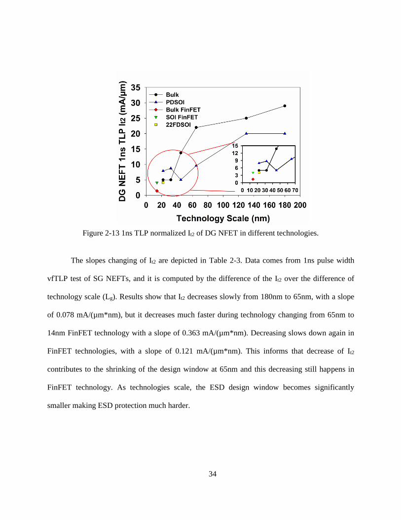
Figure 2-13 1ns TLP normalized It2 of DG NFET in different technologies. .............................. 34
Figure 2-14 1ns TLP calculated Vt2 of SG NFET in different bulk technologies. ....................... 35
Figure 2-15 1ns TLP calculated Vt2 of SG NFET in different SOI technologies. ........................ 36
Figure 2-16 1ns TLP calculated Vt2 of DG NFET in different bulk technologies. ....................... 36

xii
Figure 2-17 1ns TLP calculated Vt2 of DG NFET in different SOI technologies. ....................... 37
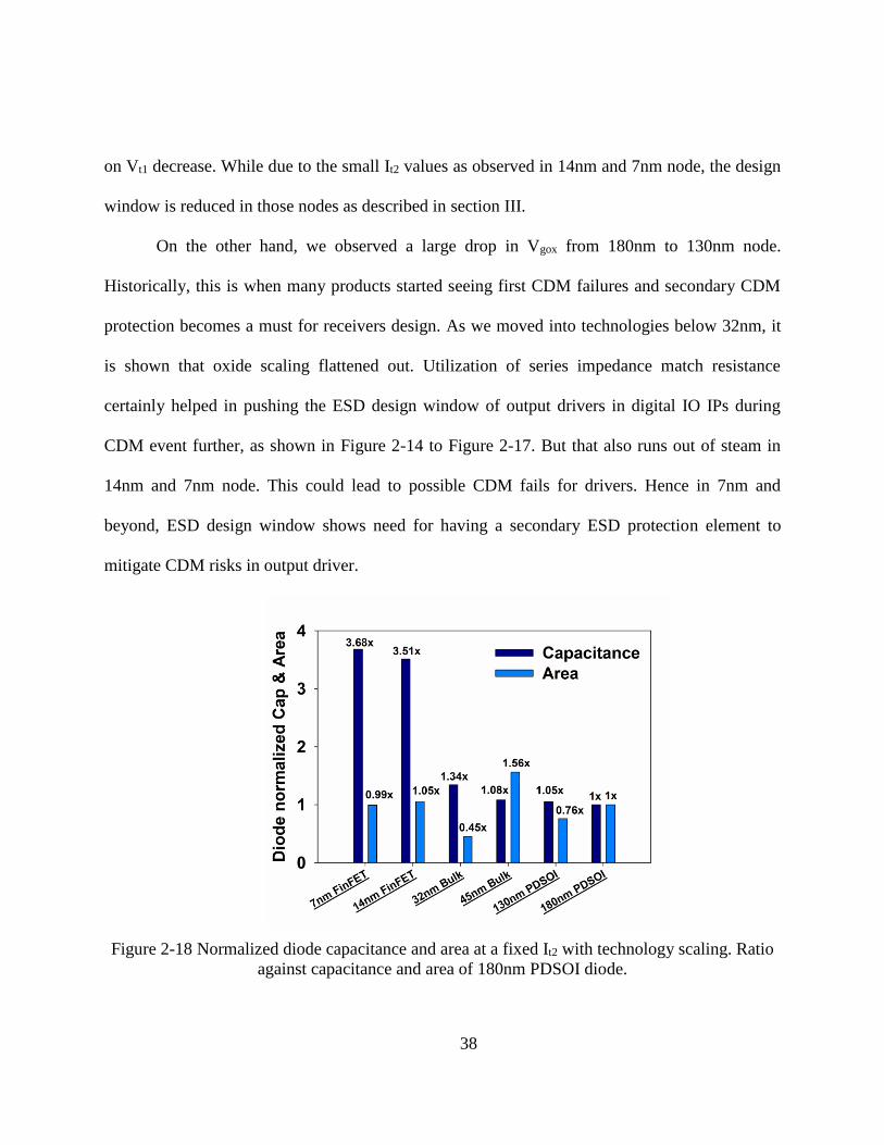
Figure 2-18 Normalized diode capacitance and area at a fixed It2 with technology scaling. Ratio
against capacitance and area of 180nm PDSOI diode. ................................................................. 38
Figure 2-19 Normalized current handling ability (current/width of the metal (A/µm)) of metal
line. Ratio against current handling ability of 32nm M1. ............................................................. 39
Figure 3-1 Stacked diodes used as ESD protection cell at I/O pads. ............................................ 41
Figure 3-2 Proposed DD-SCR integrated as part of an example of high data rate I/O ESD
protection cell................................................................................................................................ 42
Figure 3-3 Cross section views of (a) single diode (b) N+/ PW stacked diodes (c) P+/NW stack
diodes (d) STI-bounded DD-SCR (e) metal-bounded DD-SCR, and (f) junction-bounded DD-
SCR. The cells have eight fingers and a total width of 40 µm. .................................................... 46
Figure 3-4 (a) Capacitance vs. voltage characteristic of STI-bounded, metal-bounded, junction-
bounded DD-SCRs and single diode measured at 100 kHz. (b) Capacitance versus frequency of
STI bounded DD-SCR and Metal bounded DD-SCR. The devices capacitance shows little
variation over the frequency range of interest up to 60 GHz. ....................................................... 48
Figure 3-5 TLP I-V curves of STI-bounded, metal-bounded, junction-bounded DD-SCRs,
P+/NW stacked diodes, and N+/PW stacked diodes. TLP pulse width was 100ns and rise time
was 0.6ns. ...................................................................................................................................... 49
Figure 3-6 vfTLP I-V curves of STI-bounded, metal-bounded, junction-bounded DD-SCRs,
P+/NW stacked diodes, N+/PW stacked diodes and single diode. The vfTLP pulse width is 5ns
and rise time is 0.1ns. .................................................................................................................... 51

xiii
Figure 3-7 vfTLP voltage waveforms of STI-bounded, metal-bounded, junction-bounded DD-
SCRs, P+/NW stacked diodes, N+/PW stacked diodes and single diode. The vfTLP pulse width
is 5ns and rise time is 0.1ns. The overshoot is corresponding to a pulse current level of 1A. ..... 52
Figure 3-8 DC I-V curves measured at (a) 25 and (b) 125 of STI-bounded, metal-bounded,
junction-bounded DD-SCRs and P+/NW stacked diodes. ............................................................ 53
Figure 4-1 ESD protection cell connected in RF I/O. ................................................................... 56
Figure 4-2 Proposed distributed network and its mechanism. ...................................................... 57
Figure 4-3 A proposed network structure with dev I in the first stage and dev II in the following
stages. ............................................................................................................................................ 58
Figure 4-4 Protected circuit that needs low holding voltage protection cell. ............................... 59
Figure 4-5 Cross section view of Dev I (view in path A direction). ............................................. 60
Figure 4-6 Cross section view of Dev II (view in path A direction). ........................................... 60
Figure 4-7 CV measurement of Dev I and Dev II when frequency at 100 KHz. ......................... 61
Figure 4-8 Positive TLP 100-ns-wide 10-ns rise-time measurements of Dev I and Dev II. ........ 62
Figure 4-9 Test and simulation S11 results of Dev I and Dev II. ................................................. 63
Figure 4-10 (a) Layout of 0.5 nH inductor; (b) inductance simulation results. ............................ 64
Figure 4-11 Positive TLP 100-ns-wide 10-ns rise-time measurements of two-stage, three-stage
and four-stage network. ................................................................................................................ 65
Figure 4-12 Positive vfTLP 5-ns-wide 0.3-ns rise-time measurements of two-stage, three-stage
and four-stage network. ................................................................................................................ 65
Figure 4-13 Positive vfTLP 5-ns-wide 0.3-ns rise-time measurements of three-stage network
with L2 = 0.1 nH and L1 variation. .............................................................................................. 66

xiv
Figure 4-14 Waveform under positive vfTLP 5-ns-wide 0.3-ns rise-time measurements of three-
stage network with L2 = 0.1 nH and L1 variation. Current level = 1A. ....................................... 66
Figure 4-15 Simulation S11 versus L1 variation of three-stage network, with L2 fixed at 0.1nH.
....................................................................................................................................................... 67
Figure 4-16 Test S11 versus L1 variation of three-stage network, with L2 fixed at 0.1nH. ........ 68
Figure 4-17 Test S11 versus L2 variation of three-stage network, with L1 fixed at 0.5nH. ........ 70
Figure 4-18 Test S11 versus L1 variation of three-stage network, with L2 fixed at 1nH. ........... 70
Figure 4-19 Test S11 versus L1 variation of two-stage network. ................................................. 71
Figure 5-1 Cross section view of tradition stacking SCR-SCR (CS SCR-SCR). ......................... 75
Figure 5-2 Cross section view of proposed stacking SCR-LVTSCR (PS SCR-LVTSCR). ......... 75
Figure 5-3 Triggering methodology of conventional and proposed structure. ............................. 76
Figure 5-4 DC results of single SCR, CS SCR-SCR and PS SCR-LVTSCR. ............................. 77
Figure 5-5 TLP results of single SCR, CS SCR-SCR and PS SCR-LVTSCR. Test pulse is 100ns
width, and rise time is 2ns............................................................................................................. 78
Figure 5-6 TLP results of PS SCR-LVTSCR with 2, 3 and 4 stacking devices. Test pulse is
100ns width, and rise time is 2ns. ................................................................................................. 79
xv
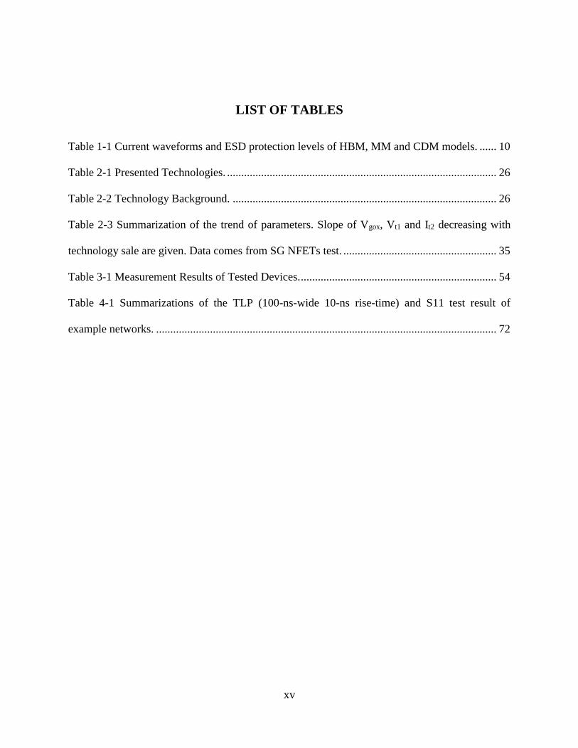
LIST OF TABLES
Table 1-1 Current waveforms and ESD protection levels of HBM, MM and CDM models. ...... 10
Table 2-1 Presented Technologies. ............................................................................................... 26
Table 2-2 Technology Background. ............................................................................................. 26
Table 2-3 Summarization of the trend of parameters. Slope of Vgox, Vt1 and It2 decreasing with
technology sale are given. Data comes from SG NFETs test. ...................................................... 35
Table 3-1 Measurement Results of Tested Devices. ..................................................................... 54
Table 4-1 Summarizations of the TLP (100-ns-wide 10-ns rise-time) and S11 test result of
example networks. ........................................................................................................................ 72

xvi
LIST OF ACRONYMS
ADC
BCD
BJT
Analog to Digital Converter
Bipolar-CMOS-DMOS
Bipolar Junction Transistor
CDM Charged Device Model
CMOS
DD-SCR
DTSCR
Complementary Metal-Oxide-Semiconductor
Dual-Diode Silicon Controlled Rectifier
Diode String Trigged SCR
DUT Device Under Test
ESD Electrostatic Discharge
FDSOI
FET
FICDM
Fully Depleted Silicon on Insulator
Field-Effect Transistor
Field-Induced Charged Device Model
GGNMOS Grounded-Gate N-type MOSFET
HBM
HPPI
HSS
Human Body Model
High Power Pulse Instruments
High Speed Serial
IC
I/O
JEDEC
Integrated Circuit
Input/Output
Joint Electron Device Engineering Council
LVTSCR Low Voltage Triggering Silicon Controlled Rectifier

xvii
MM
PDSOI
PIN
RF
Machine Model
Partially Depleted Silicon on Insulator
P-type/Intrinsic/N-type
Radio Frequency
SCR
SOI
SPICE
Silicon Controlled Rectifier
Silicon on Insulator
Simulation Program with Integrated Circuit Emphasis
TCAD Technology Computer Aided Design
TLP
vfTLP
Transmission Line Pulse
very-fast-TLP
1
CHAPTER 1 INTRODUCTION
1.1 ESD Event and Protection Methodology
Electrostatic discharge (ESD) is defined as the transfer of charge between objects at
different potentials in a quite short time. ESD events not only occur in the dry cold winter day
when someone reaches the metal handle of his or her house door, but also can occur throughout
the whole life of an integrated circuit (IC) product from the manufacturing, testing, shipping,
handing, to end user operating stages. Damages introduced by ESD events results in a loss of
millions dollars to the semiconductor industry each year. It has been reported that more than 35%
of the failures in integrated circuits are ESD induced. Therefore, the ESD related failure is a
major IC reliability concern and this is particularly true as microelectronics technology continues
shrink to nano-metric dimensions.
The duration of ESD stress is as short as nanosecond (ns) to millisecond (ms)[1], which is
one of its major characteristics. Besides, ESD stress has high energy, which could results in a
high voltage at the level of a few kilovolts (kV) and large current at the level of tens of amps (A).
Such a high voltage and large current induced by ESD could cause serious damages to
semiconductor device or circuits. The example of silicon and metal damages induced by ESD
stress are shown in Figure 1-1 [2] and Figure 1-2 [3] respectively.
Due to the concerns of ESD damages, ESD protection is very important and gradually get
more attentions with technology development. For example in 7nm FinFET technologies, the
FET device is much vulnerable to ESD stress and can barely handling any ESD current. Thus,
sufficient ESD protections in advanced technologies are extremely important and highly
demanded.

2
The basic idea of ESD protection design is during ESD event, it adds a path with a low
impedance to shunt the ESD current away from the internal core circuit as well as to clamp the
I/O and power pad voltage to a relative safe level, while during normal circuit operation, it is
transparent to internal circuit. Requirements for idea ESD protection design include zero on-
resistance, finite clamping voltage, small footprint, instantaneous turn-on time (~1ns), no leakage
current, no parasitic capacitance, and surviving the burn-in test etc.
Figure 1-1 Drain junction damage induced by ESD stress.
Figure 1-2 Metal melt damage by ESD stress.
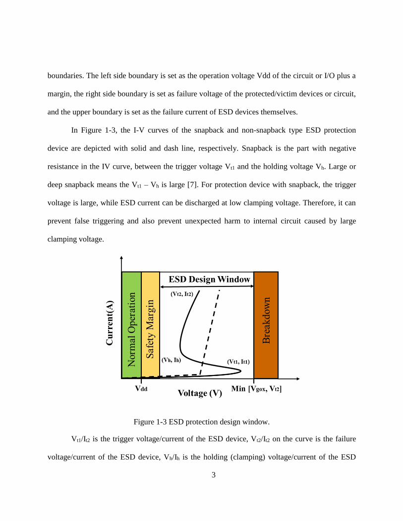
ESD protection design should fit in the ESD design window [4-6]. Figure 1-3 shows the
scheme of ESD design window. ESD design window defines the boundaries in which ESD
device and circuit have to operate for effective protection. To provide a successful ESD
protection, ESD device should turn on and clamp the voltage within the design window
3
boundaries. The left side boundary is set as the operation voltage Vdd of the circuit or I/O plus a
margin, the right side boundary is set as failure voltage of the protected/victim devices or circuit,
and the upper boundary is set as the failure current of ESD devices themselves.
In Figure 1-3, the I-V curves of the snapback and non-snapback type ESD protection
device are depicted with solid and dash line, respectively. Snapback is the part with negative
resistance in the IV curve, between the trigger voltage Vt1 and the holding voltage Vh. Large or
deep snapback means the Vt1 – Vh is large [7]. For protection device with snapback, the trigger
voltage is large, while ESD current can be discharged at low clamping voltage. Therefore, it can
prevent false triggering and also prevent unexpected harm to internal circuit caused by large
clamping voltage.
Figure 1-3 ESD protection design window.
Vt1/It2 is the trigger voltage/current of the ESD device, Vt2/It2 on the curve is the failure
voltage/current of the ESD device, Vh/Ih is the holding (clamping) voltage/current of the ESD

4
device, and Vgox/Vt2 on the x-axis is gate oxide breakdown voltage/failure voltage of the victim
device. In order to prevent latch-up, the holding voltage of protection device should be larger
than Vdd plus a safety margin voltage (typically 10% of Vdd). On the other hand, the ESD
protection device should be triggered before the damage of the victim device, thus the trigger
voltage of ESD device should be smaller than the Vgox or Vt2 of the victim device.
1.2 ESD Models
ESD event can happen in different occasions such as semiconductor manufacturing,
measurement and applications. In these procedures, static charges can accumulate in different
objects, such as human body, manufacturing machine or IC itself. Discharge happens when the
charged objects contact a grounded surface, and the discharge waveforms are different since the
corresponding equivalent capacitance and resistance can vary a lot in different discharging paths.
To standardize the designing and measurement process of ESD protection, semiconductor
manufacturers and ICs design house have derived several ESD stress models and test methods to
mimic the ESD events in real world. Typical ESD models include human body mode (HBM),
machine model (MM), and charged device model (CDM) [3]. Testing techniques such as
Transmission Line Pulse (TLP) Tester are also proposed. These ESD models and test methods
produce repeatable discharge pulses to evaluate the robustness of ESD protection structures
under different ESD stress. Standardization groups such as ESD Association (ESDA) and Joint
Electron Device Engineering Council (JEDEC) are continuously reviewing and re-edit these
models and providing corresponding protection levels to specify globally applied test standards.

5
1.2.1 Human Body Model
Figure 1-4 A simplified equivalent circuit of HBM.
Figure 1-5 Current waveform of HBM when VHBM = 2KV.

6
The HBM model is the most classical and commonly used discharge model in
semiconductor industry. HBM simulates the ESD event which occurs when a charged person
touches a device. Typically, it has a rise time of 2 to 10 ns, and a pulse duration of 130 to 170 ns
[8]. Figure 1-4 shows an equivalent circuit of the HBM, which has a simple RC network to
simulate the discharge from a human body. Two key elements including equivalent body
resistance and equivalent body to ground capacitance are 1500 Ω and 100pF, respectively. The
primary standards of HBM include JEDEC/ESDA JS-001-2017 [9] and JEDEC JEP155A.01
[10], etc. Current waveform of HBM when VHBM equals to 2KV is shown in Figure 1-5, the peak
current of this stress can be 1.33A. In HBM testing, IC failure modes typically show gate oxide,
contact spike, and junction damage.
1.2.2 Machine Model
Figure 1-6 A simplified equivalent circuit of MM.
7
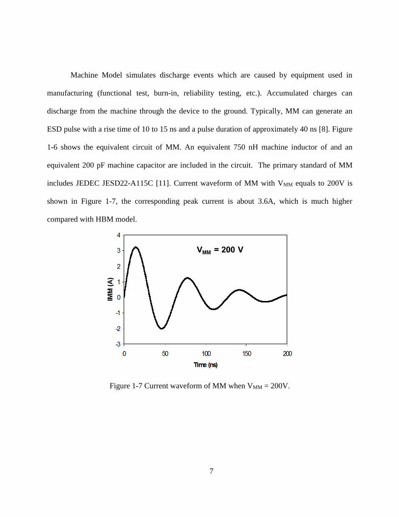
Machine Model simulates discharge events which are caused by equipment used in
manufacturing (functional test, burn-in, reliability testing, etc.). Accumulated charges can
discharge from the machine through the device to the ground. Typically, MM can generate an
ESD pulse with a rise time of 10 to 15 ns and a pulse duration of approximately 40 ns [8]. Figure
1-6 shows the equivalent circuit of MM. An equivalent 750 nH machine inductor of and an
equivalent 200 pF machine capacitor are included in the circuit. The primary standard of MM
includes JEDEC JESD22-A115C [11]. Current waveform of MM with VMM equals to 200V is
shown in Figure 1-7, the corresponding peak current is about 3.6A, which is much higher
compared with HBM model.
Figure 1-7 Current waveform of MM when VMM = 200V.

8
1.2.3 Charged Device Model
Figure 1-8 A simplified equivalent circuit of CDM.
Figure 1-9 Current waveform of CDM when VCDM = 500V.

9
CDM simulates the ESD event occurring when a charged device is discharged to a
metallic ground. The electrostatic discharge of CDM happens from the inside of IC to the outside
ground. CDM has a rise time of 100ps to 500ps and a pulse duration of under 1ns [8]. Figure 1-8
shows an equivalent circuit of CDM, and Figure 1-9 shows the typical current waveform of
CDM. The primary standard of CDM includes ESDA/JEDEC JS-002-2014 [12]. CDM currents
are higher than HBM currents because there is no current limiting resistor in the discharge path.
For a 500V test voltage, the peak current can goes to 6A.
1.2.4 ESD Model Comparison
Figure 1-10 Current waveform comparison of HBM, MM and CDM model.
Figure 1-10 and Table 1-1 compares the different current waveforms of HBM, MM, and
CDM models. As shown in Figure 1-10, the higher parasitic capacitance and lower overall
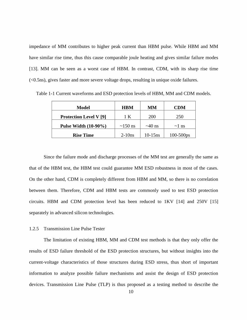
10
impedance of MM contributes to higher peak current than HBM pulse. While HBM and MM
have similar rise time, thus this cause comparable joule heating and gives similar failure modes
[13]. MM can be seen as a worst case of HBM. In contrast, CDM, with its sharp rise time
(<0.5ns), gives faster and more severe voltage drops, resulting in unique oxide failures.
Table 1-1 Current waveforms and ESD protection levels of HBM, MM and CDM models.
Model HBM MM CDM
Protection Level V [9] 1 K 200 250
Pulse Width (10-90%) ~150 ns ~40 ns ~1 ns
Rise Time 2-10ns 10-15ns 100-500ps
Since the failure mode and discharge processes of the MM test are generally the same as
that of the HBM test, the HBM test could guarantee MM ESD robustness in most of the cases.
On the other hand, CDM is completely different from HBM and MM, so there is no correlation
between them. Therefore, CDM and HBM tests are commonly used to test ESD protection
circuits. HBM and CDM protection level has been reduced to 1KV [14] and 250V [15]
separately in advanced silicon technologies.
1.2.5 Transmission Line Pulse Tester
The limitation of existing HBM, MM and CDM test methods is that they only offer the
results of ESD failure threshold of the ESD protection structures, but without insights into the
current-voltage characteristics of those structures during ESD stress, thus short of important
information to analyze possible failure mechanisms and assist the design of ESD protection
devices. Transmission Line Pulse (TLP) is thus proposed as a testing method to describe the

11
behaviors of device under ESD stress by characterizing current-voltage curves and leakage
current information. Figure 1-11 shows the simplified equivalent circuit of TLP. The principle
for TLP testing is to produce a stable square waveform to stress the device under test (DUT) and
record the respond curve across the DUT as shown in Figure 1-12. Typically, the TLP tester
begins with low voltage pulses and successively increases in amplitude with a certain voltage
step. The transmission line is firstly charged by a high voltage DC source first, and the charged
transmission line discharges through DUT. Key ESD parameters could be obtained from the TLP
measurement, including trigger voltage/current Vt1/It1, holding voltage/current Vh/Ih, failure
voltage/current Vt2/It2, DC leakage current, on-resistance RON and DC breakdown voltage
VBD.
Figure 1-11 A simplified equivalent circuit of TLP tester.

12
Figure 1-12 TLP tester measures I and V at each voltage pulse.
TLP could generate a ESD-like pulse with a rise time of 0.5 to 10 ns and a pulse width of
50 to 150 ns [8, 16]. A typical rise time of 10 ns and pulse width of 100 ns is usually used to
correlate the HBM. Another test method, named very fast TLP (vfTLP) testing, can describe the
transient behavior of ESD protection structures for CDM application [17]. In this work, some of
the measurements were performed by the Barth 4002 transmission line pulsing (TLP) and Barth
4012 very fast transmission line pulsing (vfTLP) testers, some were performed by high power
pulse instruments (HPPI) TLP/vfTLP test system.
1.3 ESD Protection Device
To avoid or reduce the ESD failure in ICs, two methods are widely used in
semiconductor industry. One is using static control and awareness programs to reduce the build-
up of static charges and the IC ESD exposure. It can be achieved by improving the
manufacturing working environments, such as wearing wrist strap, covering work surface by
conductive material, and neutralizing all insulator materials with ionizer [18, 19]. The other
method is implementing ESD protection devices and circuits to shunt high discharge current and

13
keep ESD strikes away from protected internal circuit during ESD event. ESD protection level
can be significantly increased by adding proper ESD protection structures, resulting in improved
reliability of the ICs and electronic systems.
This work is focusing on the second method: several improved on-chip ESD protection
structures are proposed to enhance the robustness of the IC. These structures are modified from
the basic ESD protection devices, including diode, Grounded Gate N-type MOSFET (GGNMOS)
and Silicon Controlled Rectifier (SCR) [8]. Basic ESD devices can be divided as non-snapback
device and snapback device. Among the three basic protection structures, diode is non-snapback
device, while GGNMOS and SCR are snapback devices.
ESD protection structures should fit in the design window shown in Figure 1-3, and an
ideal ESD protection devices prefer to have zero on-resistance, finite clamping voltage, small
footprint, instantaneous turn-on time (~1ns), no leakage current, no parasitic capacitance, and
surviving the burn-in test. In this section, we will introduce the structures of the basic ESD
protection devices and their operation and parasitic characteristics under ESD events.

14
1.3.1 Diode
Figure 1-13 Cross section view of a P+/NW diode.
Figure 1-14 Cross section view of a series diode.
Because of its simple structure and good performance, the junction diode is widely used
for ESD protection at I/O pins of integrated circuits. The cross section views of P+/NW and
series diode are shown in Figure 1-13 and Figure 1-14, respectively. The parasitic capacitance of
diode is the junction capacitance Cj [20, 21], which is determined by the area of the junction. By
stacking the diode in series, the capacitance can be greatly minimized [22]. Diodes especially
series diode (stacking) are popular in high frequency circuit protection due to its less capacitive
characteristic.

15
The TLP I-V curve of diode is shown in Figure 1-15. This diode is fabricated in 28nm
technology. Diode is no-snapback device. The trigger voltage of the forward biased junction
diode is about 0.7V. After triggering, the diode can conduct significant current with very low on-
state resistance.
Figure 1-15 TLP characteristics of diode.
1.3.2 GGNMOS
Due to GGNMOS has simple structure and it is compatible with CMOS technology, it is
also a popular device in ESD protection [23]. GGNMOS is modified from the normal NMOS
device. In GGNMOS, the drain of NMOS serves as the anode, and the shorted gate, source and
body contact are tied together to serve as the cathode. Figure 1-16 shows the equivalent circuit
and cross section view with of a GGNMOS. When ESD pulse stresses on the drain contact of
GGNMOS, drain voltage increases and leads to an increasing substrate current. The current

16
contribute to the increasing bias (VBE) at the PW/N+ junction. When VBE of the parasite
bipolar junction transistor (BJT) exceeds 0.7 V, the parasite NPN turns on to sink ESD current.
After trigger of GGNMOS, the GGNMOS goes into snapback operation region due to the bipolar
action in the device. With drain voltage further increases, it finally reaches the thermal failure.
The parasitic capacitance of GGNMOS comes from junction capacitance Cj and gate
capacitance Cg. Figure 1-17 shows the equivalent parasitic capacitance of GGNOMS. Cj and Cg
are connected in parallel, thus the total capacitance equals to Cj + Cg. Besides, Cg is much larger
than Cj. Under same condition, the parasitic capacitance of GGNOMS is much larger diode and
SCR. Therefore in high frequency circuit ICs, GGNMOS is seldom used.
Figure 1-16 Equivalent circuit and cross section view with parasite NPN of a GGNMOS.
Figure 1-17 Equivalent parasitic capacitance of GGNMOS.
17
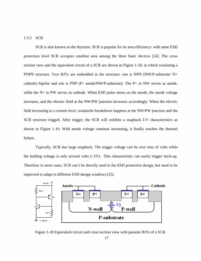
1.3.3 SCR
SCR is also known as the thyristor. SCR is popular for its area efficiency: with same ESD
protection level SCR occupies smallest area among the three basic devices [24]. The cross
section view and the equivalent circuit of a SCR are shown in Figure 1-18, in which consisting a
PNPN structure. Two BJTs are embedded in the structure: one is NPN (NW/P-substrate/ N+
cathode) bipolar and one is PNP (P+ anode/NW/P-substrate). The P+ in NW serves as anode,
while the N+ in PW serves as cathode. When ESD pulse stress on the anode, the anode voltage
increases, and the electric field at the NW/PW junction increases accordingly. When the electric
field increasing to a certain level, avalanche breakdown happens at the NW/PW junction and the
SCR structure trigged. After trigger, the SCR will exhibits a snapback I-V characteristics as
shown in Figure 1-19. With anode voltage continue increasing, it finally reaches the thermal
failure.
Typically, SCR has large snapback. The trigger voltage can be over tens of volts while
the holding voltage is only several volts (~2V). This characteristic can easily trigger latch-up.
Therefore in most cases, SCR can’t be directly used in the ESD protection design, but need to be
improved to adapt to different ESD design windows [25].
Figure 1-18 Equivalent circuit and cross section view with parasite BJTs of a SCR.

18
Figure 1-19 TLP characteristics of SCR.
Similar with diode, the parasitic capacitance of SCR is junction capacitance of PW/NW
Cj. Capacitance can be minimized by minimizing the junction area of PW/NW. SCR is also a
popular ESD protection in high frequency circuit application [26].
1.4 ESD Protection Circuit
ESD current will flow through the paths of least resistance, thus efficient low resistance
discharge devices that can carry high current should be properly placed for circuit level
protection. According to the ESD testing standards, to adequately protect the ICs from ESD
damage, an ESD protection network must provide the current discharge path between any two
pins. Typical ESD protection schemes can be divided to VDD-based and VSS-based protection
scheme, which is shown in Figure 1-20 [27-29]. Both of the schemes have placed proper clamp
between any combination of I/O, Vdd, Vss, such as I/O-to-VDD, I/O-to-VSS, I/O-to-I/O, and
VDD-to-VSS [30] to protect positive or negative ESD discharge between them.
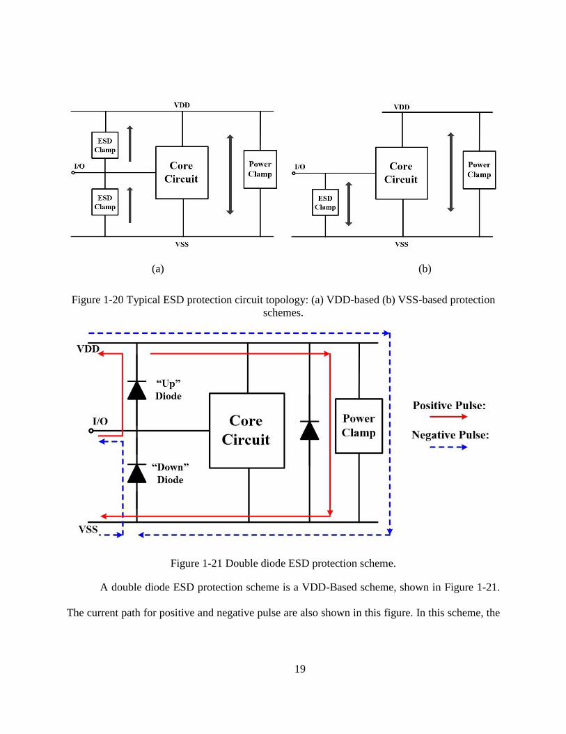
19
(a) (b)
Figure 1-20 Typical ESD protection circuit topology: (a) VDD-based (b) VSS-based protection
schemes.
Figure 1-21 Double diode ESD protection scheme.
A double diode ESD protection scheme is a VDD-Based scheme, shown in Figure 1-21.
The current path for positive and negative pulse are also shown in this figure. In this scheme, the

20
I/O voltage must remain between VDD + Vdiode and VSS – Vdiode, otherwise the protection
diode will forward biased (Vdiode is the diode forward biased voltage, ~0.7V).
Figure 1-22 GGNMOS ESD protection scheme.
Figure 1-23 SCR ESD protection scheme.

21
GGNMOS and SCR ESD protection schemes are shown in Figure 1-22 and Figure 1-23
respectively. These two schemes are VSS-Based protection scheme and share the similar current
discharge path. In these two protection scheme, the I/O voltage can rise above the power supply
without sinking DC current into the signal pin. For low voltage I/O protection, diode string
trigged SCR (DTSCR) is typically used in the SCR scheme, since DTSCR has a much lower
trigger voltage compared with SCR.
In applications, the choice of the protection schemes can vary according to the design
window and available protection devices.
1.5 Summary and Dissertation Outline
ESD related failure is a major IC reliability concern and this is particularly true as
microelectronics technology continues shrink to nano-metric dimensions. This chapter introduces
the ESD fundamentals: several ESD stress models and on-chip ESD protection structures are
discussed which are helpful to understand this dissertation. ESD models are developed by
semiconductor industry to simulate the real world ESD phenomenon and ESD protection
schemes are introduced to effectively protect the IC from ESD induced damage.
The organization of the dissertation is as follow. Chapter 2 starts with reviewing ESD
Design window across multiple technologies. The requirement to lower the HBM and CDM
level further for FinFET technologies is discussed in details. Chapter 3 presents a dual diode
SCR (DD-SCR) structure. It also compares DD-SCRs with different bounding materials. These
designs can exhibit good ESD performance and low parasitic capacitance characteristics. Chapter
4 investigates an inductor embedded π-network and its design methodology. The π-networks
22
work well for RF applications in the 7.5 GHz to 62 GHz frequency range. Chapter 5 present a
resistor-assist triggering heterogeneous stacking structure, which can minimize the snapback of
SCR device. Chapter 6 comes summary and conclusion of the dissertation.

23
CHAPTER 2 STUDY OF ESD DESIGN WINDOW SCALING DOWN
TO 7NM TECHNOLOGY NODE
2.1 Introduction
ESD design window defines the boundaries which ESD device and circuit have to
operate in for effective protection. To provide a successful ESD protection, ESD device should
turn on and clamp the voltage within the design window boundaries. Figure 1-3 shows the
illustration of the ESD design window. It is clearly shown that the left side boundary is set as the
operation voltage Vdd of the circuit or I/O plus a margin, the right side boundary is set as failure
voltage of the protected/victim devices or circuit, and the upper boundary is set as the failure
current of ESD devices themselves [4-6]. Since the left side boundary is fixed for a certain
technology, and the upper boundary depends on ESD cell itself, knowing the right side boundary
is critical to define the margin of the ESD design window.
Figure 2-1 shows typical I/O schematics protected by ESD cells [31, 32]. In Figure 2-1,
the gate oxide breakdown voltage Vgox of the victim FET that connects with CDM network
defines the right side boundary of design window. On the other hand, the ESD event may turn on
the victim FET that is connected with the I/O, therefore in this case the failure voltage Vt2 of the
victim FET defines the right side boundary. One challenge for ESD design is that Vgox and Vt2 of
FET keep decreasing with technology scaling. At the same time, normalized failure current (It2)
is degrading, thus causing ESD design window to shrink drastically.
24
Figure 2-1 Typical I/O schematics. Rs in the red dash line is the series resistor that can extend
Vt2. Victim FETs in the Green dash line.
In this paper, the trend of design window scaling across bulk, silicon on insulator (SOI)
and FinFET technologies in technology nodes from 350nm to 7nm is studied. Transmission line
pulse (TLP) and very-fast-TLP (vfTLP) testing results of gate oxide breakdown voltage Vgox,
trigger voltage Vt1, and normalized failure current It2 of silicided thin oxide (SG) and thick oxide
(DG) NFETs and PFETs (victim devices), are given and discussed. Calculated failure voltage Vt2
with different series resistors Rs (shown in Figure 2-1) are also presented to evaluate the potential
of ESD design window extension. For the first time, all these parameters are reviewed and
compared across multiple technology generations to establish the fact that digital drivers are

25
becoming vulnerable to CDM test and High-Speed Serial (HSS) designs may need a lower CDM
target level for FinFET and beyond technologies due to device capacitance increase as
technologies scale.
2.2 Technology Background
FETs of multiple generations of planar bulk, planar SOI and FinFETs are characterized in
this paper. Figure 2-2 shows representative 3-D structures of a FET in bulk, SOI and FinFET
technologies.
Bulk
SOI
Gate
N+
Psub
STI
Bulk FinFET
SOI FinFET
Figure 2-2 3-D structure of NFETs in bulk, SOI and FinFET technology.
Data presented in this work is based on GlobalFoundries’ developed process. Technology
nodes introduced are 350nm, 180nm, 130nm, 65nm, 45nm, 32nm, 22nm, 14nm, and 7nm. Planar
bulk and partially depleted silicon on insulator (PDSOI) are used in technologies from 180nm to
22nm. Besides, one bulk technology in 350nm and one FDSOI technology in 22nm are
considered. For FinFET technology, SOI FinFET technology in 14nm and bulk FinFET in both

26
14nm and 7nm are presented as well. The summary table is shown in Table 2-1 and Table 2-2
along with various process elements that are included in each node.
Table 2-1 Presented Technologies.
Technology
(nm)
350 180 130 65 45 32 22 14
(FinFET)
7
(FinFET)
Bulk × × × × × × × × ×
PDSOI × × × × × × ×
FDSOI ×
Table 2-2 Technology Background.
Nodes --> ≥45nm 32nm 22nm 14nm 7nm
Feature Bulk PDSOI Bulk PDSOI Bulk PDSOI FDSOI Bulk
FinFET
SOI
FinFET
Bulk
FinFET
Poly Gate x x x
Metal First
Metal Gate High
K Dielectric
x x
Thin BOX x
Replacement
Metal Gate High
K Dielectric
x x x x x
Trench Silicide x x
Epi S/D x x x x
Gate length (Lg) and gate thickness (Tox) are both scaling down with technology trend [33,
34]. Figure 2-3 and Figure 2-4 show the evolution of Tox in each technology (normalized) for SG
and DG respectively. Tox of SG and DG follows similar trend with technology scale: it is
observed that the oxide thickness scales down as we move from 350nm to smaller technology
node leading to a plateau around 65nm. After that it follows a less drastic slope, which can be
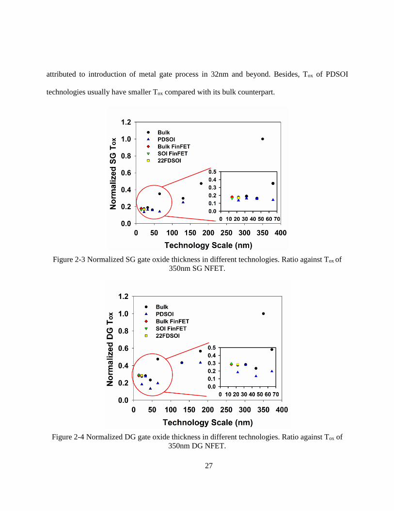
27
attributed to introduction of metal gate process in 32nm and beyond. Besides, Tox of PDSOI
technologies usually have smaller Tox compared with its bulk counterpart.
Figure 2-3 Normalized SG gate oxide thickness in different technologies. Ratio against Tox of
350nm SG NFET.
Figure 2-4 Normalized DG gate oxide thickness in different technologies. Ratio against Tox of
350nm DG NFET.

28
2.3 Trend of Parameters
Victim NFETs and PFETs with width ranging from 50µm to 200µm, and finger-number
ranging from 1 to 5 are measured and compared in this section. Several key parameters for ESD
design window are covered, including Vgox, Vt1, It2 and calculated Vt2 of both NFET and PFET.
100ns TLP and 1ns vfTLP measurements are used for characterization. The results are depicted
in Figure 2-5 to Figure 2-17. A summarization of Vgox, Vt1 and It2 decreasing slope across the
technology scale is given in Table 2-3.
Gate oxide breakdown voltage Vgox is critical when characterizing the right side boundary
of design window. In Vgox measurement, source and drain of FET are connected together as one
terminal and gate of FET is the other terminal. The trends of how Vgox vary under 100ns TLP
measurement for both SG NFET and SG PFET are presented in Figure 2-5 and Figure 2-6,
respectively. Besides, result of DG NFET is present in Figure 2-7.
Figure 2-5 100ns TLP gate oxide breakdown voltage of SG NFET in different technologies.

29
Figure 2-6 100ns TLP gate oxide breakdown voltage of SG PFET in different technologies.
Figure 2-7 100ns TLP gate oxide breakdown voltage of DG NFET in different technologies.
It is observed that there is almost an 8X reduction of oxide breakdown voltage from
350nm node to 7nm node in SG FET. Due to technology scaling and introduction of metal gates,
for advanced technology nodes between 22nm (FDSOI) to 7nm (FinFET), the gate oxide
breakdown voltage of SG reduces significantly but stays within 2.5V-3V range. Due to larger Tox,

30
Vgox of DG NEFT on the other hand, drops significantly before 65nm, while stay stable within
6V to 8V in advanced technology nodes. Considering the operation voltages of SG and DG are
typically 0.9V and 1.5V respectively, these low Vgox in advanced technologies drive a significant
reduction in the ESD design window.
The slopes of Vgox of SG NEFTs across the technology are depicted in Table 2-3. Data
comes from 100ns pulse width TLP test, and it is computed by the difference of the Vgox over the
difference of technology scale (Lg). Results show that Vgox decreases fast from 180nm to 65nm,
with a slope of 0.059 V/nm, and it continues decreasing with a slope of 0.031 V/nm during
technology changing from 65nm to 14nm FinFET technology. However, the decreasing stops in
FinFET technologies, with a negative slope of -0.014 V/nm, indicating Vgox slightly increase in
FinFET technologies.
Vt1 is defined by the voltage between drain and source, at which the parasitic NPN can be
triggered by an ESD event and go into avalanche breakdown mode. In the measurement, gate is
connected with source as one terminal and drain is the other terminal. The trends of 100ns TLP
trigger voltage Vt1 of SG NFET/PFET and DG NFET in different technologies are shown in
Figure 2-8, Figure 2-9 and Figure 2-10 respectively.
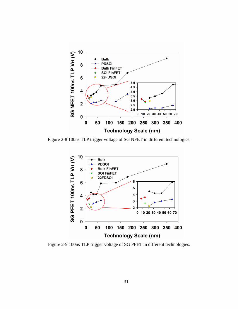
31
Figure 2-8 100ns TLP trigger voltage of SG NFET in different technologies.
Figure 2-9 100ns TLP trigger voltage of SG PFET in different technologies.

32
Figure 2-10 100ns TLP trigger voltage of DG NFET in different technologies.
The slopes of Vt1 of SG NEFTs across the technology are depicted in Table 2-3. Data
comes from 1ns pulse width vfTLP test, and it is computed by the difference of the Vt1 over the
difference of technology scale (Lg). Results show that Vt1 decreases slowly from 180nm to 65nm,
with a slope of 0.015 V/nm, but it decreases faster during technology changing from 65nm to
14nm FinFET technology with a slope of 0.035 V/nm. As Vgox, decreasing stop also happens in
Vt1 in FinFET technologies, with a negative slope of -0.043 V/nm. This confirms that Vt1 within
FinFET technologies stay stable and even slightly increase when changing from 14nm to 7nm.
Failure current It2 defines how much ESD current a victim FETs can handle after
triggering. Normalized It2 of silicided SG NFETs/PFETs and DG NFETs under 1ns vfTLP are
shown in Figure 2-11, Figure 2-12 and Figure 2-13 respectively. It2 of NFETs is higher than
PFETs in most of the technologies. It2 of NFETs is approximately 30mA/μm in bulk 180nm
technology, which keeps decreasing across various technology nodes leading to ~6X decrease at
20nm node (the last planar technology node). It2 for FinFETs showed an even further dip and a
33
reduction of another ~4X when compared against 20nm bulk/PDSOI technology. In bulk
technology, the slope of It2 decreasing in 65nm to 32nm segment is almost 9X compared with
180nm to 65nm segment, indicating failure current decreases more quickly in advanced
technologies.
Figure 2-11 1ns TLP normalized It2 of SG NFET in different technologies.
Figure 2-12 1ns TLP normalized It2 of SG PFET in different technologies.
34
Figure 2-13 1ns TLP normalized It2 of DG NFET in different technologies.
The slopes changing of It2 are depicted in Table 2-3. Data comes from 1ns pulse width
vfTLP test of SG NEFTs, and it is computed by the difference of the It2 over the difference of
technology scale (Lg). Results show that It2 decreases slowly from 180nm to 65nm, with a slope
of 0.078 mA/(µm*nm), but it decreases much faster during technology changing from 65nm to
14nm FinFET technology with a slope of 0.363 mA/(µm*nm). Decreasing slows down again in
FinFET technologies, with a slope of 0.121 mA/(µm*nm). This informs that decrease of It2
contributes to the shrinking of the design window at 65nm and this decreasing still happens in
FinFET technology. As technologies scale, the ESD design window becomes significantly
smaller making ESD protection much harder.
35
Table 2-3 Summarization of the trend of parameters. Slope of Vgox, Vt1 and It2 decreasing with
technology sale are given. Data comes from SG NFETs test.
Slope v.s. Tech 7nm-14nm 14nm-65nm 65nm-180nm
Vgox (100ns) -0.014 0.031 0.059
Vt1 (1ns) -0.043 0.035 0.015
It2 (1ns) 0.121 0.363 0.078
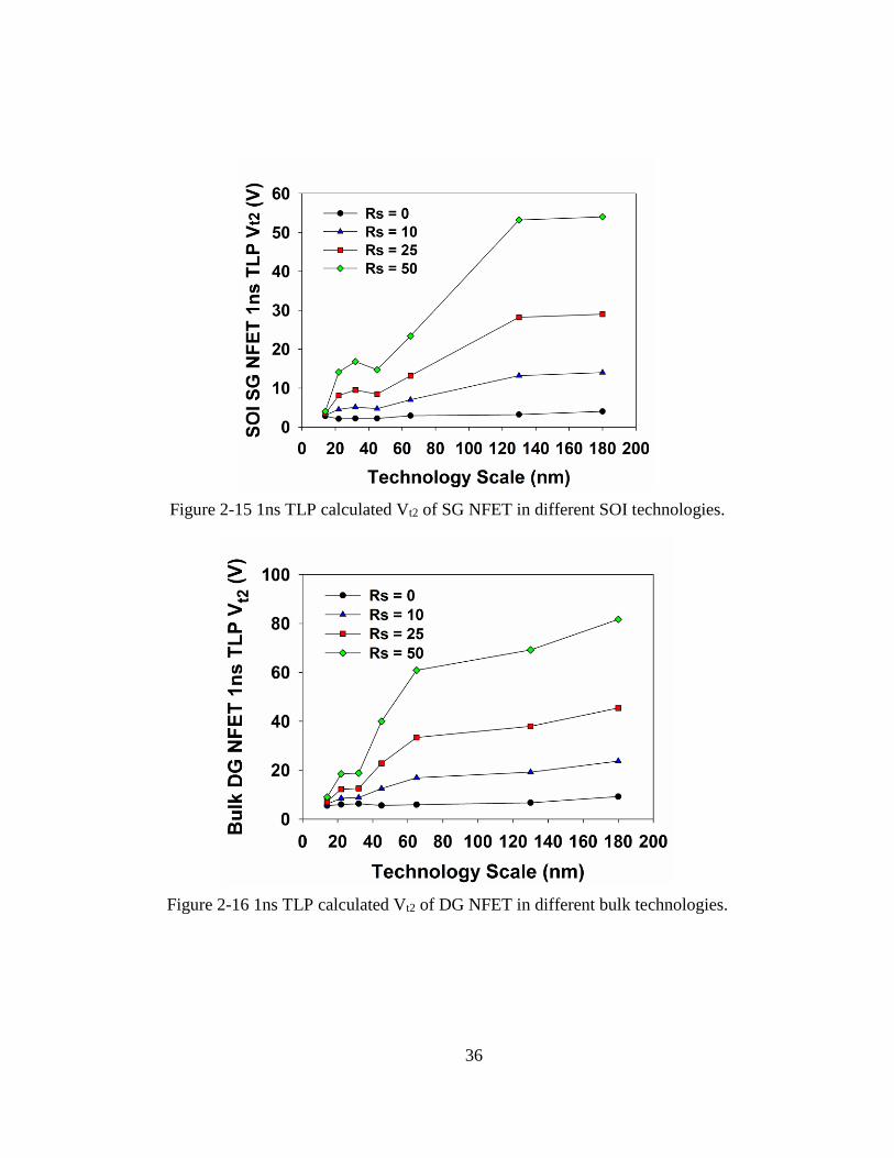
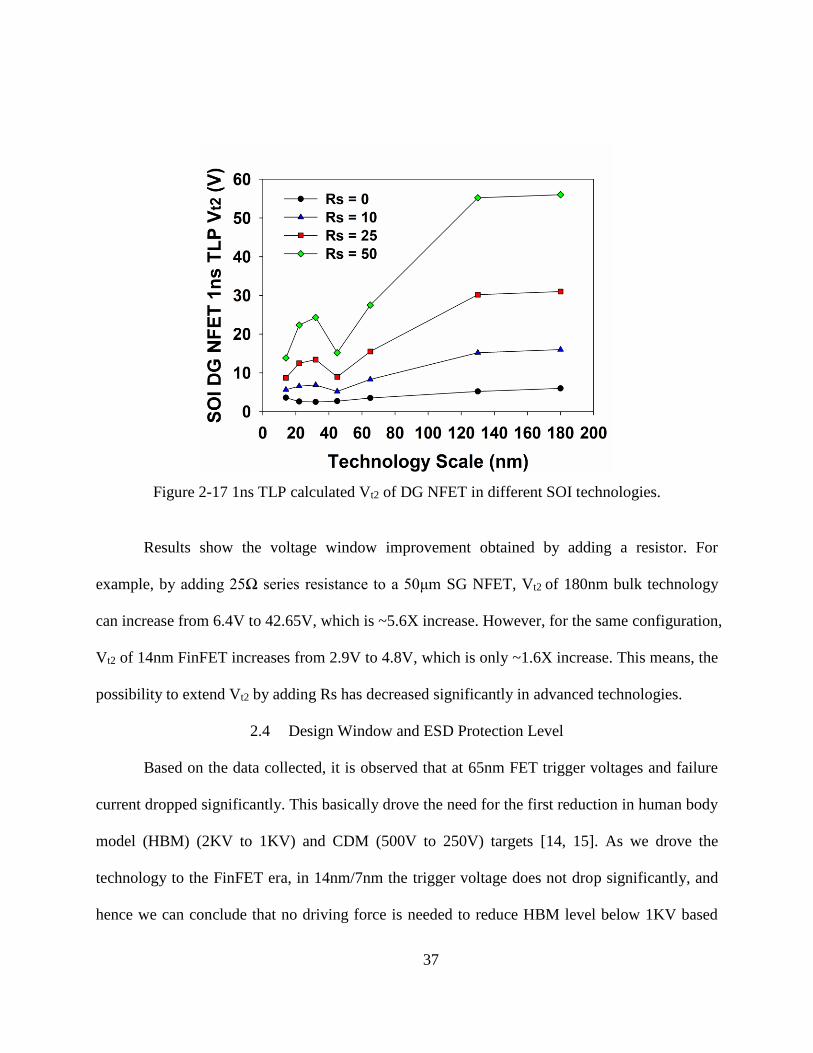
Final failure voltage (Vt2) of bulk and SOI technologies are shown in Figure 15 to Figure
18, to evaluate the potential of further extending ESD design window.
As shown in Figure 2-1, having a resistance (Rs) in series with the victim FET would
increase Vt2, which can be calculated as:
Vt2 = Vt1 + It2×W×Rs (1)
where It2 is normalized per µm width of the FET, W is the total gate width of the FET in
µm. In Figure 2-14 to Figure 2-17, calculated Vt2 for various Rs (0 Ω, 10 Ω, 25 Ω, 50 Ω) are
presented. The W used in the calculation is 50μm.
Figure 2-14 1ns TLP calculated Vt2 of SG NFET in different bulk technologies.
36
Figure 2-15 1ns TLP calculated Vt2 of SG NFET in different SOI technologies.
Figure 2-16 1ns TLP calculated Vt2 of DG NFET in different bulk technologies.
37
Figure 2-17 1ns TLP calculated Vt2 of DG NFET in different SOI technologies.
Results show the voltage window improvement obtained by adding a resistor. For
example, by adding 25Ω series resistance to a 50μm SG NFET, Vt2 of 180nm bulk technology
can increase from 6.4V to 42.65V, which is ~5.6X increase. However, for the same configuration,
Vt2 of 14nm FinFET increases from 2.9V to 4.8V, which is only ~1.6X increase. This means, the
possibility to extend Vt2 by adding Rs has decreased significantly in advanced technologies.
2.4 Design Window and ESD Protection Level
Based on the data collected, it is observed that at 65nm FET trigger voltages and failure
current dropped significantly. This basically drove the need for the first reduction in human body
model (HBM) (2KV to 1KV) and CDM (500V to 250V) targets [14, 15]. As we drove the
technology to the FinFET era, in 14nm/7nm the trigger voltage does not drop significantly, and
hence we can conclude that no driving force is needed to reduce HBM level below 1KV based
38
on Vt1 decrease. While due to the small It2 values as observed in 14nm and 7nm node, the design
window is reduced in those nodes as described in section III.
On the other hand, we observed a large drop in Vgox from 180nm to 130nm node.
Historically, this is when many products started seeing first CDM failures and secondary CDM
protection becomes a must for receivers design. As we moved into technologies below 32nm, it
is shown that oxide scaling flattened out. Utilization of series impedance match resistance
certainly helped in pushing the ESD design window of output drivers in digital IO IPs during
CDM event further, as shown in Figure 2-14 to Figure 2-17. But that also runs out of steam in
14nm and 7nm node. This could lead to possible CDM fails for drivers. Hence in 7nm and
beyond, ESD design window shows need for having a secondary ESD protection element to
mitigate CDM risks in output driver.
Figure 2-18 Normalized diode capacitance and area at a fixed It2 with technology scaling. Ratio
against capacitance and area of 180nm PDSOI diode.

39
Figure 2-19 Normalized current handling ability (current/width of the metal (A/µm)) of metal
line. Ratio against current handling ability of 32nm M1.
High-Speed Serial (HSS) interface design in advanced ASIC design drives very low
capacitance loading while meeting required ESD protection level. High data rates (>20Gb/s)
applications limits the ESD loading capacitance to be less than 100 fF [35, 36]. In addition, a
similar or even larger footprint of ESD diode is required due to transition from planar to FinFET
technology to achieve the same ESD level, shown in Figure 2-18. It requires ESD robustness to
an optimal level but drives the capacitance load to a higher value which is problematic for HSS
interface designs [21, 37]. A Figure of Merit (FOM) is used to describe this concern, as shown in
Figure 2-18. Based on the FOM (calculated as total capacitance for a given It2), it is observed
that ~3X increase of ESD component capacitance while transitioning from planer (45nm-32nm)
to FinFET (14nm-7nm) nodes. This clearly dictates a direction towards further lowering of the
HBM and CDM targets for HSS interface designed for 14nm and beyond technologies.
Another risk is the decreasing of metal current handling ability in FinFET technology. As
depicted in Figure 2-19, in 14nm FinFET node, current handling ability of first level metal has

40
decreased to ~60-70% compared with 32nm node. This leads to having larger metal width
requirement to meet the same ESD current handling limit, which in turn drives a larger
capacitance loading or higher Vdd/Vss resistance for the same metal width. This create
additional challenges for both digital and HSS interface design.
2.5 Conclusion
Vgox, Vt1, It2 and calculated Vt2 of FET were measured and reviewed across multiple
generations of technologies. Results indicated that ESD design window based on Vt1 and Vgox is
shrinking drastically with technology scaling. It is shown that for technologies where the
silicided victim FETs can handle ESD current, the design window can be expanded significantly
by using impedance matching resistances in series with the driver. There could be a need for
having secondary protection for drivers in 7nm and beyond to meet CDM protection level for
digital design. On the other hand, for high speed designs, one needs to consider lowering the
HBM and CDM level further for FinFET technologies as ESD device capacitance loading
becomes significantly higher while no improvement observed in Vt1 or It2 for FETs.

41
CHAPTER 3 DUAL-DIODE SCR WITH REDUCED CAPACITANCE
AND OVERSHOOT VALTAGE FOR HIGH SPEED INTERFACE
APPLICATIONS
3.1 Introduction
Along with the design of high speed data rate integrated circuits and the development of
advanced process technology, integrating ESD protection at high speed communication
Input/Output (I/O) pins draws increasing attentions in the literature [38-46]. Protection solutions
are often limited by a variety of design trade-offs for narrow- and wide- band I/Os applications
[39-46]. As an example, common design constraints include the inability to incorporate passive
devices as part of the interface circuit protection, the complexity to optimize the design of a
custom device in a new process, and the negative consequences of the protection components on
performance. This is because in addition to the requirement of ESD robustness, parasitic
capacitance, can be detrimental to the interface circuit signal processing integrity [42-47].
Figure 3-1 Stacked diodes used as ESD protection cell at I/O pads.

42
Figure 3-2 Proposed DD-SCR integrated as part of an example of high data rate I/O ESD
protection cell.
Figure 3-1 shows an ESD protection structure consisting of stacked diodes [48]. Under
normal operating conditions, the diodes are reverse biased and hence in the off-state. During an
ESD stress, the diodes forward bias and divert the ESD-induced current away from the internal
circuit. The drawbacks of such a structure include the relatively large on-state resistance and

43
added complexity in optimizing the interconnect metallization parasitic, in particular for
advanced CMOS process technologies [45].
An alternative to addressing the limitations of the conventional stacked diode protection
architecture consists of merging the stacked diodes into a single structure. Doing so can create a
parallel conduction path, improving the ESD performance and reducing the protection cell
capacitance [48-51]. However, the specific design trade-off in these structures can vary
substantially depending on process technology and application of concern.
Figure 3-2 shows the ESD protection scheme proposed for a data-communication
interface circuit. For instance, this can include an analog to digital (ADC) input buffer interface,
with a voltage swing in the range of ± 0.5 V, an input buffer power bias between -1V and 2.5 V,
and data rate up to 10 GBPS. Note that particularly critical for this application is the capacitance
linearity versus the voltage, as this affects the degree of distortion.
In this particular reference design, a new dual-diode silicon controlled rectifier (DD-SCR)
is included as protection element at the input pin. Notice that the input pin is directly connected
through an RC circuit to the input gate transistors.
Due to stringent distortion design constraint in high data rate applications, the value and
linearity in the input capacitance introduced by the protection elements in this broadband
functionality circuit is required to be under 40 fF, with an allowance of less than 2 fF capacitance
variation within the operating voltage range. As for the leakage current, it is specified to be less
than 10 nA. In addition, during the stress condition, the cell should have the ability to withstand a
stress of ~ 1000 V HBM [14]. Furthermore, for robustness under Field-Induced Charged Device

44
Model (FICDM), the protection devices are required to respond sufficiently fast to prevent a
large voltage overshoot at the interface pin [52].
This work present three optimized variations of an interface ESD protection structure
composed of dual diodes embedded with a silicon controlled rectifier (DD-SCR) and reviews the
design trade-offs for high data rate communication applications. Section II introduces the DD-
SCR structures, this is followed by a review of the experimental results in Section III. The latter
includes capacitance, DC, and transmission line pulse (TLP) measurements. The TLP
measurements emulate the response of the devices when subject to the human body model (HBM)
and charged device model (CDM), respectively. Section IV concludes with the discussion of the
design trade-offs between the different DD-SCR structures presented.
3.2 Device Structure
Figure 3-3 (a)-(f) show the cross-sectional views of single diode, stacked diodes, STI-
bounded DD-SCR, metal-bounded DD-SCR, and junction-bounded DD-SCR cells, respectively.
In stacked diodes and DD-SCRs, two diodes are connected in series between the terminals T1
and T2, and all the DD-SCRs have a SCR embedded in the structure (see the equivalent circuit
annotated in Figure 3-3(d) and (e)). When an ESD stress is applied to terminal T1, the diodes
conduct first due to the low forward-biased turn-on voltage of approximately 1.9V. Once the
diodes are triggered, the current flowing through the NW and PW regions turns on the SCR.
There is also a parasitic SCR structure (P+/NW/Psub/N+) in the P+/NW stacked diodes, which
can increase the overall capacitance and affect the turn-on performance of the devices. In the STI
DD-SCR, this parasitic phenomenon is less prominent.

45
The common features of the three DD-SCR cells are the following:
1) Terminal T1 connects to the lower-level metal (metal 2) and terminal T2 connects to
the upper-level metal (metal 8), a configuration that could minimize the capacitance between the
two terminals;
2) The two diodes are formed by P+/NW and N+/PW junctions; and
3) DNW is used to isolate the active region from the substrate.
The difference between the metal-bounded and STI-bounded cells is that the former uses
a metal layer as a spacer between the N+ and P+ regions instead of an STI. As will be shown
later, the different bounded structures give rise to different capacitance, overshoot voltage and
on-state resistance RON, characteristics [53]. On the other hand, the locations of the P+ and N+
regions of metal-bounded and STI-bounded cell are also different, thereby resulting in different
SCR current paths compared with the other two DD-SCRs and thus different trigger voltages and
ESD robustness.
For the junction-bounded cell, its main difference compared with STI-bounded cell is that
the N+ of the first diode and the P+ of the second diode are connected together, and the N+ is
placed across the NW and PW with a distance D (D = 0.2 µm is used in the measurements in
Section III). This will affect overshoot voltage and capacitance.
All the cell layouts are designed in similar dimensions in order to make useful
comparisons. The lengths of NW and PW regions are 1.5µm, and lengths of P+ and N+ regions
are 0.6µm for all the cells, except for the junction-bounded DD-SCR, whose N+ region has a
length of 0.78µm. For the single diode and the stacked diodes, a spacing of 0.8µm between the
NW regions is used as required by the process design rules. The P+ guard ring was not included
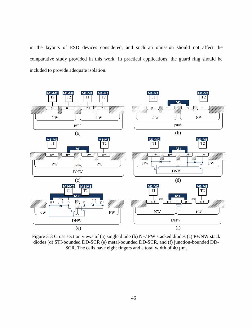
46
in the layouts of ESD devices considered, and such an omission should not affect the
comparative study provided in this work. In practical applications, the guard ring should be
included to provide adequate isolation.
(a)
(b)
(c)
(d)
(e)
(f)
Figure 3-3 Cross section views of (a) single diode (b) N+/ PW stacked diodes (c) P+/NW stack
diodes (d) STI-bounded DD-SCR (e) metal-bounded DD-SCR, and (f) junction-bounded DD-
SCR. The cells have eight fingers and a total width of 40 µm.
47
3.3 Experimental Result
The capacitance versus voltage measurement for each device is obtained between the
terminals T1 and T2 at 100KHz in Figure 3-4 (a). The extra capacitance associate with the bond-
pads and metallization outside the device is de-embedded during open calibration. Using a
network analyzer and de-embedding method, the capacitances of the STI bounded and metal
bounded DD-SCRs are also measured at frequencies up to 60GHz, as shown in Figure 3-4 (b).
For reference, the capacitances of all the three the DD-SCRs variations are about half of the
corresponding capacitance of a single diode, since there are two diode stacked together in the
DD-SCR structure, this effectively includes two diodes in series. As shown in Figure 3-4 (a),
among the three DD-SCRs, the STI-bounded cell has the lowest capacitance, followed by the
junction-bounded cell, with the metal-bounded cell having the largest capacitance. This trend
suggests that using the metal as a bounding material will give rise to a larger capacitance,
because such a cell results in a spherical junction and consequently a larger effective junction
area than the flat junction of the STI-bounded cell. In light of this, the capacitances of the metal-
bounded and junction-bounded DD-SCR are larger than that of the STI-bounded DD-SCR.
In addition, a small spacing between the neighboring terminal metal lines (lines
connected to the T1 and T2 terminals) can also contributes to an additional capacitance. This
phenomenon is observed in the metal-bounded cell. The relatively narrow spacing between the
two terminals of this cell leads to the largest capacitance among all of the three cells.
The capacitance of the STI-bounded DD-SCR is smaller than that of P+/NW stacked
diodes due to the fact that the parasitic SCR in the P+/NW stacked diodes introduce a relatively
large capacitance to the cell.

48
Voltage(V)
-4-3-2-10
Cap
acit
an
ce (
fF)
10
20
30
40STI-bounded
Metal-bounded
Junction-bounded
Single Diode
(a)
Frequency (Ghz)
10 20 30 40 50 60
Ca
pa
cit
an
ce
(fF
)
10
20
30
40
50
60
STI bounded DD-SCR
Metal bounded DD-SCR
(b)
Figure 3-4 (a) Capacitance vs. voltage characteristic of STI-bounded, metal-bounded, junction-
bounded DD-SCRs and single diode measured at 100 kHz. (b) Capacitance versus frequency of
STI bounded DD-SCR and Metal bounded DD-SCR. The devices capacitance shows little
variation over the frequency range of interest up to 60 GHz.
The capacitance of all three DD-SCRs is less than 25fF at 100KHz Capacitance versus
Voltage test. Among them, the STI-bounded DD-SCR has the lowest capacitance and can be the
most appropriate choice if a low parasitic capacitance is desired. A trade-off between the

49
capacitance and ESD performance exists, since the lower capacitance device also will have a
higher on-state resistance when subject to stress.
Figure 3-5 compares the transmission line pulsed (TLP) characterization for the different
devices. Based on the TLP testing results, the DD-SCRs depict a smaller RON and larger It2 than
the stacked diodes. The SCR embedded in the structures provides an alternative conduction path
deeper into the silicon. This enhances the device current handling capability. In addition, among
the three DD-SCRs, the STI-bounded SCR shows a much larger on-resistance than the metal-
bounded and junction-bounded devices.
Figure 3-5 TLP I-V curves of STI-bounded, metal-bounded, junction-bounded DD-SCRs,
P+/NW stacked diodes, and N+/PW stacked diodes. TLP pulse width was 100ns and rise time
was 0.6ns.
The STI increases the length of the current conduction path, which explains the larger
RON. For the metal-bounded cell, the distance between the P+ and N+ diffusions in the SCR path
is shorter, resulting in a larger It2 and smaller RON.

50
A large RON will negatively impact the ESD protection robustness, since it leads to a
higher voltage drop across the protection cell when conducting the same level of current. This
will make the protected pin more vulnerable to the ESD stress. Based on this consideration, the
metal-bounded cell and junction-bounded cells would be a better choice.
Generally speaking, the smaller the RON, the larger the It2. This is because a larger RON
can lead to a larger voltage drop, which increases the power dissipation in the ESD cell and
causes the protection cell to reach its thermal breakdown at a lower current level. Thus, the
metal-bounded and junction-bounded cells exhibit higher ESD robustness than the STI-bounded
cell and stacked diodes.
Figure 3-6 shows the vfTLP results. The trend of It2 is consistent with that obtained from
the TLP testing, with the metal-bounded DD-SCR shows the highest ESD robustness and the
stacked diodes having a lower It2 than the DD-SCRs. Results obtained from the single diode
subject to the vfTLP stress have also been added. The single diode possesses a slightly lower It2
and larger RON than the junction bounded DD-SCR and metal bounded DD-SCR.
The overshoot voltage is a key parameter for evaluating the effectiveness for CDM
protection. Achieving a low overshoot voltage is highly desired [41, 51, 52]. Overshoot voltages
of the three DD-SCR and stacked-diode cells, measured using the Barth Electronics TLP system,
are compared in Figure 3-7. Note that the stacked-diodes and STI-bounded DD-SCR cells have a
larger overshoot voltage than the metal-bounded and junction-bounded DD-SCR devices.
Besides, the single diode performs almost the same as the junction bounded DD-SCR and metal
bounded DD-SCR.

51
Figure 3-6 vfTLP I-V curves of STI-bounded, metal-bounded, junction-bounded DD-SCRs,
P+/NW stacked diodes, N+/PW stacked diodes and single diode. The vfTLP pulse width is 5ns
and rise time is 0.1ns.
To design an ESD device with a low overshoot voltage, an approach is to reduce the
length of the trigger current path, where STI bounding material shows its drawbacks compared
with metal bounding material. Among the proposed DD-SCRs, the STI bounded cell has the
longer current path due to its deep STIs, thus the higher overshoot voltage. On the other hand,
the junction-bounded cell lacks the STIs and hence provides the shortest current path among DD-
SCRs and also making its overshoot voltage comparable with single diode. Moreover, in the
junction-bounded DD-SCR cell, the N+ is overlapping the NW and PW diffusions, making the
embedded SCR triggers at a lower voltage with a reduced overshoot voltage.
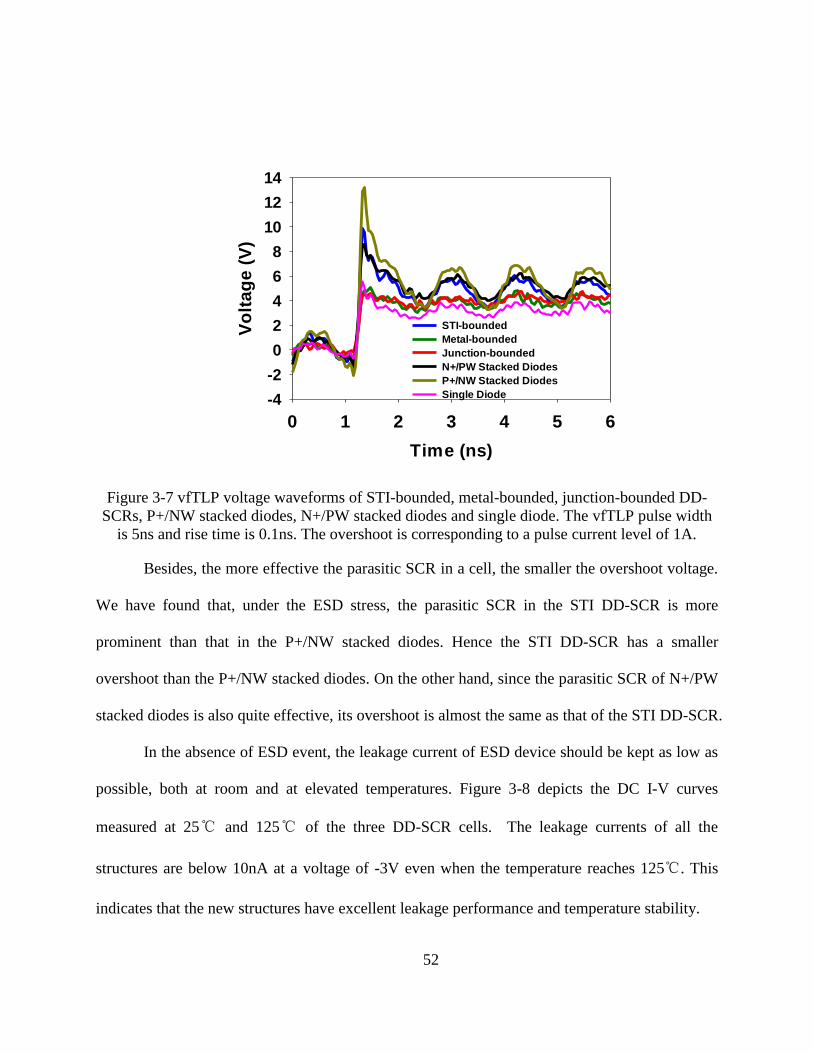
52
Time (ns)
0 1 2 3 4 5 6
Vo
lta
ge
(V
)
-4
-2
0
2
4
6
8
10
12
14
STI-bounded
Metal-bounded
Junction-bounded
N+/PW Stacked Diodes
P+/NW Stacked Diodes
Single Diode
Figure 3-7 vfTLP voltage waveforms of STI-bounded, metal-bounded, junction-bounded DD-
SCRs, P+/NW stacked diodes, N+/PW stacked diodes and single diode. The vfTLP pulse width
is 5ns and rise time is 0.1ns. The overshoot is corresponding to a pulse current level of 1A.
Besides, the more effective the parasitic SCR in a cell, the smaller the overshoot voltage.
We have found that, under the ESD stress, the parasitic SCR in the STI DD-SCR is more
prominent than that in the P+/NW stacked diodes. Hence the STI DD-SCR has a smaller
overshoot than the P+/NW stacked diodes. On the other hand, since the parasitic SCR of N+/PW
stacked diodes is also quite effective, its overshoot is almost the same as that of the STI DD-SCR.
In the absence of ESD event, the leakage current of ESD device should be kept as low as
possible, both at room and at elevated temperatures. Figure 3-8 depicts the DC I-V curves
measured at 25 and 125 of the three DD-SCR cells. The leakage currents of all the
structures are below 10nA at a voltage of -3V even when the temperature reaches 125. This
indicates that the new structures have excellent leakage performance and temperature stability.

53
Voltage (V)
-4 -3 -2 -1 0 1
Cu
rre
nt
(A)
1e-14
1e-13
1e-12
1e-11
1e-10
1e-9
1e-8
1e-7
1e-6
1e-5
1e-4
STI-bounded
Metal-bounded
Junction-bounded
P+/NW Stacked Diodes
(a)
Voltage (V)
-4 -3 -2 -1 0 1
Cu
rre
nt
(A)
1e-12
1e-11
1e-10
1e-9
1e-8
1e-7
1e-6
1e-5
1e-4
STI-bounded
Metal-bounded
Junction-bounded
P+/NW Stacked Diodes
(b)
Figure 3-8 DC I-V curves measured at (a) 25 and (b) 125 of STI-bounded, metal-bounded,
junction-bounded DD-SCRs and P+/NW stacked diodes.
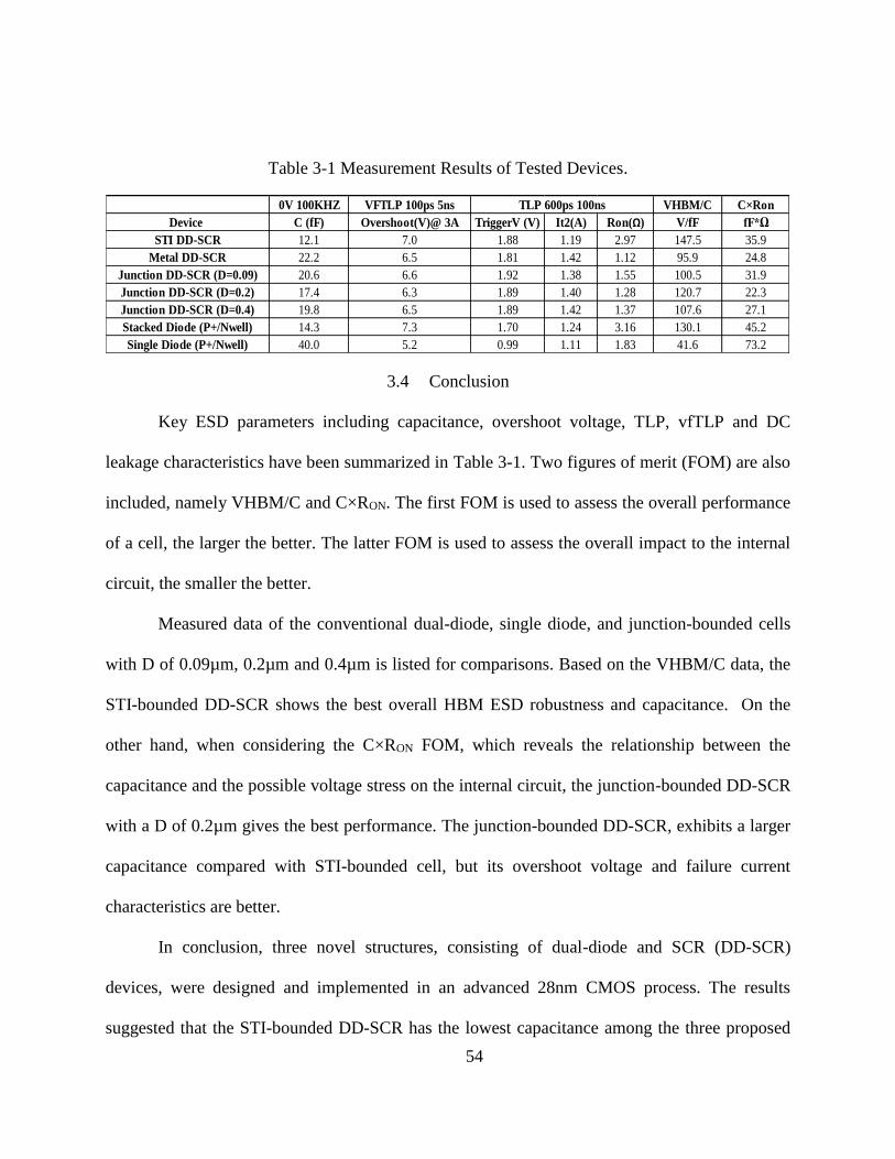
54
Table 3-1 Measurement Results of Tested Devices.
0V 100KHZ VFTLP 100ps 5ns VHBM/C C×Ron
Device C (fF) Overshoot(V)@ 3A TriggerV (V) It2(A) Ron(Ω) V/fF fF*Ω
STI DD-SCR 12.1 7.0 1.88 1.19 2.97 147.5 35.9
Metal DD-SCR 22.2 6.5 1.81 1.42 1.12 95.9 24.8
Junction DD-SCR (D=0.09) 20.6 6.6 1.92 1.38 1.55 100.5 31.9
Junction DD-SCR (D=0.2) 17.4 6.3 1.89 1.40 1.28 120.7 22.3
Junction DD-SCR (D=0.4) 19.8 6.5 1.89 1.42 1.37 107.6 27.1
Stacked Diode (P+/Nwell) 14.3 7.3 1.70 1.24 3.16 130.1 45.2
Single Diode (P+/Nwell) 40.0 5.2 0.99 1.11 1.83 41.6 73.2
TLP 600ps 100ns
3.4 Conclusion
Key ESD parameters including capacitance, overshoot voltage, TLP, vfTLP and DC
leakage characteristics have been summarized in Table 3-1. Two figures of merit (FOM) are also
included, namely VHBM/C and C×RON. The first FOM is used to assess the overall performance
of a cell, the larger the better. The latter FOM is used to assess the overall impact to the internal
circuit, the smaller the better.
Measured data of the conventional dual-diode, single diode, and junction-bounded cells
with D of 0.09µm, 0.2µm and 0.4µm is listed for comparisons. Based on the VHBM/C data, the
STI-bounded DD-SCR shows the best overall HBM ESD robustness and capacitance. On the
other hand, when considering the C×RON FOM, which reveals the relationship between the
capacitance and the possible voltage stress on the internal circuit, the junction-bounded DD-SCR
with a D of 0.2µm gives the best performance. The junction-bounded DD-SCR, exhibits a larger
capacitance compared with STI-bounded cell, but its overshoot voltage and failure current
characteristics are better.
In conclusion, three novel structures, consisting of dual-diode and SCR (DD-SCR)
devices, were designed and implemented in an advanced 28nm CMOS process. The results
suggested that the STI-bounded DD-SCR has the lowest capacitance among the three proposed

55
structures, and the metal-bounded and junction-bounded DD-SCRs show robust ESD
performance with a low on-resistance, RON, high failure current It2 and low overshoot voltage. In
real circuit applications, if the capacitance is of primary concern, then the STI-bounded DD-SCR
would be a good choice. On the other hand, if an improved ESD robustness is required and some
extra capacitance can be tolerated, then the junction-bounded DD-SCR should be considered.

56
CHAPTER 4 A DISTRIBUTED SHUNT π–NETWORK FOR RF I/O
ESD PROTECTION
4.1 Introduction
With the popularity of the high frequency IC technologies, electrostatic discharge (ESD)
issues in these technologies are significant [21, 38, 40, 54-60]. Challenges for ESD - RF design
and trade-offs between RF performance and ESD robustness are expected: The RF signal
integrity will be impacted by the ESD cells capacitance load, while robust ESD cells require
larger parasitic capacitance [21].
Figure 4-1 ESD protection cell connected in RF I/O.
ESD designs for high frequency I/Os are emerging to handle these challenges. For
example, T-coil [54] and stack diode with embedded silicon controlled rectifier (SCR) [21, 55]
for under 10 GHz applications, inductor-to-ground for 17.5 to 26 GHz applications [56], diode
and SCR combination structure for 24 GHz applications [57] and inductor-triggered SCR [58]
and inductor-assisted SCR [59] for 60 GHz applications have been proposed. Besides, generic
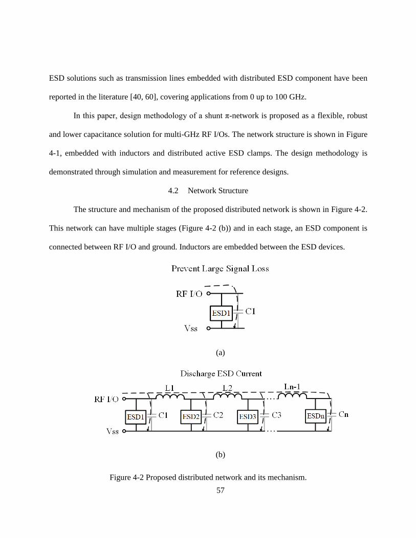
57
ESD solutions such as transmission lines embedded with distributed ESD component have been
reported in the literature [40, 60], covering applications from 0 up to 100 GHz.
In this paper, design methodology of a shunt π-network is proposed as a flexible, robust
and lower capacitance solution for multi-GHz RF I/Os. The network structure is shown in Figure
4-1, embedded with inductors and distributed active ESD clamps. The design methodology is
demonstrated through simulation and measurement for reference designs.
4.2 Network Structure
The structure and mechanism of the proposed distributed network is shown in Figure 4-2.
This network can have multiple stages (Figure 4-2 (b)) and in each stage, an ESD component is
connected between RF I/O and ground. Inductors are embedded between the ESD devices.
(a)
(b)
Figure 4-2 Proposed distributed network and its mechanism.
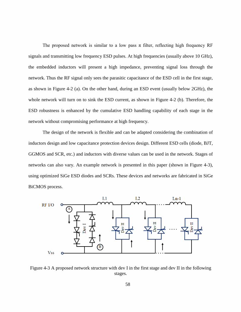
58
The proposed network is similar to a low pass π filter, reflecting high frequency RF
signals and transmitting low frequency ESD pulses. At high frequencies (usually above 10 GHz),
the embedded inductors will present a high impedance, preventing signal loss through the
network. Thus the RF signal only sees the parasitic capacitance of the ESD cell in the first stage,
as shown in Figure 4-2 (a). On the other hand, during an ESD event (usually below 2GHz), the
whole network will turn on to sink the ESD current, as shown in Figure 4-2 (b). Therefore, the
ESD robustness is enhanced by the cumulative ESD handling capability of each stage in the
network without compromising performance at high frequency.
The design of the network is flexible and can be adapted considering the combination of
inductors design and low capacitance protection devices design. Different ESD cells (diode, BJT,
GGMOS and SCR, etc.) and inductors with diverse values can be used in the network. Stages of
networks can also vary. An example network is presented in this paper (shown in Figure 4-3),
using optimized SiGe ESD diodes and SCRs. These devices and networks are fabricated in SiGe
BiCMOS process.
Figure 4-3 A proposed network structure with dev I in the first stage and dev II in the following
stages.
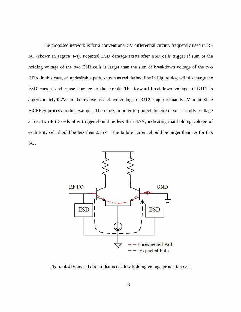
59
The proposed network is for a conventional 5V differential circuit, frequently used in RF
I/O (shown in Figure 4-4). Potential ESD damage exists after ESD cells trigger if sum of the
holding voltage of the two ESD cells is larger than the sum of breakdown voltage of the two
BJTs. In this case, an undesirable path, shown as red dashed line in Figure 4-4, will discharge the
ESD current and cause damage to the circuit. The forward breakdown voltage of BJT1 is
approximately 0.7V and the reverse breakdown voltage of BJT2 is approximately 4V in the SiGe
BiCMOS process in this example. Therefore, in order to protect the circuit successfully, voltage
across two ESD cells after trigger should be less than 4.7V, indicating that holding voltage of
each ESD cell should be less than 2.35V. The failure current should be larger than 1A for this
I/O.
Figure 4-4 Protected circuit that needs low holding voltage protection cell.

60
Figure 4-5 Cross section view of Dev I (view in path A direction).
Figure 4-6 Cross section view of Dev II (view in path A direction).
In this circuit, bidirectional ESD protection cells are needed between RF I/O and GND,
thus bi-directional ESD protection is implemented in the proposed network. As shown in Figure
4-3, Dev I and Dev II are both bidirectional, thus the network can discharge positive ESD pulses
in path A and negative ESD pulses in path B.
Cross section views of the device I (Dev I) and device II (Dev II) in the network are
shown in Figure 4-5 and Figure 4-6 separately. Figure 4-5 gives the cross section view of Dev I
(view in path A direction). In Dev I, an upper diode, an NPN triggered SCR and a lower diode
are connected in series. The complementary diode structure is used: upper diode connects RF I/O
and lower diode connects Vss, to eliminate substrate capacitance. Besides, due to the intrinsic

61
region, the diodes work like PIN diodes, thus the junction capacitance has been further
minimized. In the NPN triggered SCR, NPN with low trigger voltage and resistance R (= 250Ω)
are used to help the SCR triggering at a low voltage.
Dev II is simply an NPN triggered SCR. Figure 4-6 depicts its cross section view (view
in path A direction). This SCR has the same structure as the SCR used in Dev I, but the trigger
element is different: the trigger voltage of this NPN is higher than that in the SCR of Dev I.
Figure 4-7 CV measurement of Dev I and Dev II when frequency at 100 KHz.
Dev I is used in the first stage and Dev IIs are used in the following stages in the
proposed network. The devices arranged in this way for two reasons. First, Dev I is less
capacitive, thus placing it in the first stage will minimize the signal loss. As the CV measurement
result shown in Figure 4-7, the parasitic capacitance of Dev I is 15.2 fF at 0V compared with
122.9 fF of Dev II. Second, Dev II has smaller holding voltage (1.3V) as compared with 3.6V in
Dev I, as shown in Figure 4-8. Therefore, the total holding voltage can be reduced below the
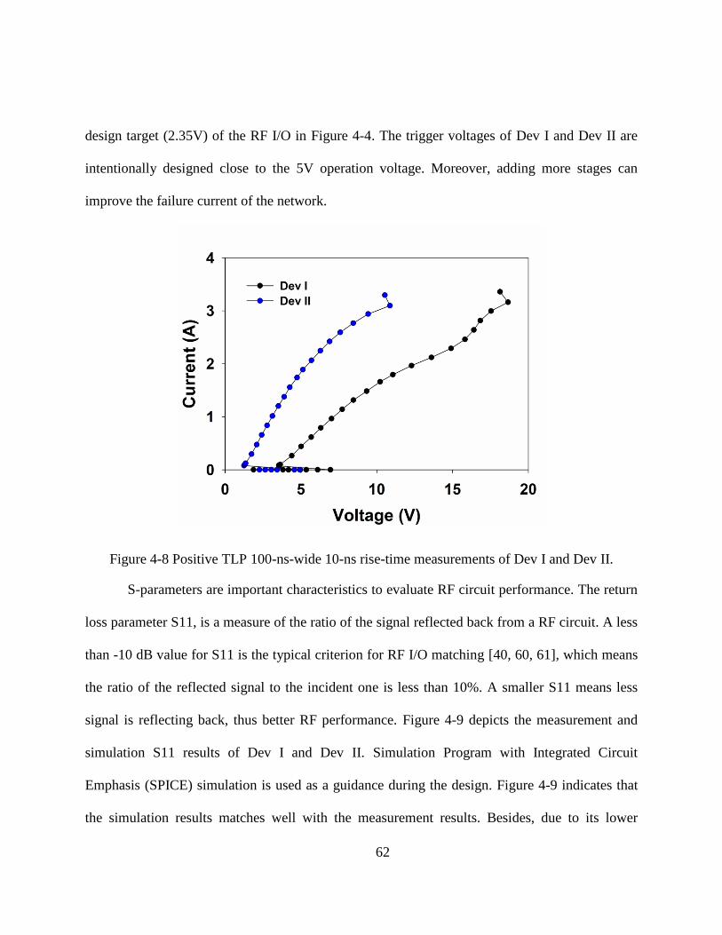
62
design target (2.35V) of the RF I/O in Figure 4-4. The trigger voltages of Dev I and Dev II are
intentionally designed close to the 5V operation voltage. Moreover, adding more stages can
improve the failure current of the network.
Figure 4-8 Positive TLP 100-ns-wide 10-ns rise-time measurements of Dev I and Dev II.
S-parameters are important characteristics to evaluate RF circuit performance. The return
loss parameter S11, is a measure of the ratio of the signal reflected back from a RF circuit. A less
than -10 dB value for S11 is the typical criterion for RF I/O matching [40, 60, 61], which means
the ratio of the reflected signal to the incident one is less than 10%. A smaller S11 means less
signal is reflecting back, thus better RF performance. Figure 4-9 depicts the measurement and
simulation S11 results of Dev I and Dev II. Simulation Program with Integrated Circuit
Emphasis (SPICE) simulation is used as a guidance during the design. Figure 4-9 indicates that
the simulation results matches well with the measurement results. Besides, due to its lower

63
parasitic capacitance, Dev I shows a less than -10 dB return loss (S11) in the range from 0 to 80
GHz, demonstrating that Dev I itself is well optimized.
Figure 4-9 Test and simulation S11 results of Dev I and Dev II.
Besides the ESD cell design mentioned above, inductor is another critical consideration,
whose value determines what frequencies can pass through the π-network. The inductors used in
the example network are square inductors. In this paper, the inductor is built to demonstrate the
mechanism network and inductor layout optimization will be presented in future work. Layout
top view of a 0.5 nH inductor is shown in Figure 4-10 (a). Simulation has been done after layout
to verify the value and the quality factor of the inductor. Figure 4-10 (b) shows the simulated
inductance as a function of frequency of three designed inductors, indicating that the inductors
are with good quality.

64
(a) (b)
Figure 4-10 (a) Layout of 0.5 nH inductor; (b) inductance simulation results.
4.3 Experimental Result
In this section, the example protection network introduced in section II are compared in
details. Figure 4-11 and Figure 4-12 show the TLP and vfTLP results of two-stage, three-stage
and four-stage network. These three networks have the same structure as the example network in
Figure 4-3. The holding voltages of the network have all been controlled to ~1.3V. Results show
that RON doesn’t vary a lot with the number of stages. RONs of the three networks are all close to
4.4Ω. This because that the resistance of the inductors will compensate the RON reduction
resulting from adding more stages. Besides, adding more ESD cells into the network indeed
increases It2, while not linearly. It2 of two-stage network is 4.5A, less than the sum of It2 of Dev I
and Dev II which is 5.6 A. The It2s of three-stage and four-stage network are both 5.9A, also
missing the linearity. This can be explained by the non-uniform turn-on and the metal line or

65
inductor burn-out of the π-network, reminding that having a deep network (> 4 stages) is not an
efficient way to enhance ESD robustness. Besides, more stages bring more design complexities,
thus limiting the stage number to be less than three is suggested.
Figure 4-11 Positive TLP 100-ns-wide 10-ns rise-time measurements of two-stage, three-stage
and four-stage network.
Figure 4-12 Positive vfTLP 5-ns-wide 0.3-ns rise-time measurements of two-stage, three-stage
and four-stage network.

66
Figure 4-13 Positive vfTLP 5-ns-wide 0.3-ns rise-time measurements of three-stage network
with L2 = 0.1 nH and L1 variation.
Figure 4-14 Waveform under positive vfTLP 5-ns-wide 0.3-ns rise-time measurements of three-
stage network with L2 = 0.1 nH and L1 variation. Current level = 1A.

67
Inductor values can affect turn on resistance (RON). Figure 4-13 and Figure 4-14 shows
the vfTLP results of the three-stage network with L1 equals to 0 nH, 0.5 nH, 1 nH and 3nH
separately. It2 doesn’t change a lot with inductor value variation, while RON is larger when larger
inductor embedded in the network. RON increase to 5.3 Ω at L1 = 3 nH, compared to 4.4 Ω at L1
= 0.5 nH. Detailed RON and It2 from TLP test results are summarized in Table 4-1. Besides,
larger inductor values also contribute to larger turn on time and larger holding voltage, as shown
in Figure 4-14.
Figure 4-15 Simulation S11 versus L1 variation of three-stage network, with L2 fixed at 0.1nH.
68
Figure 4-16 Test S11 versus L1 variation of three-stage network, with L2 fixed at 0.1nH.
Simulation and test results of S11 versus inductor variation of three-stage network are
shown in Figure 4-15 to Figure 4-18. To compared L1 variations are compared in Figure 4-15
and Figure 4-16 with L2 fixed as 0.1 nH. Figure 4-15 is circuit simulation results and Figure
4-16 is test results. Although simulation and test curves can’t perfectly overlap with each other,
simulation results is a good indicator of test results.
Results reveal that S11 curves have troughs at certain frequency and inductor values
affect the position of the trough. For example, when L1 equals to 0.6 nH and L2 equals to 0.1 nH,
network has the minimum S11 = -19 dB at 27 GHz, indicating that this network can be used in
27 GHz narrowband applications. Network with larger L1 has deeper trough in S11 curve and
the trough shifts to lower frequency. For example, when L1 equals to 5 nH, trough of S11 is -29
dB at 7.5 GHz, comparing with -19 dB at 27 GHz of a L1 = 0.6 nH network. Besides, S11 curve
69
of Dev I (dark red dash line) limits the troughs of S11 curves of networks. This demonstrates the
mechanism of the network mentioned in Figure 4-2. In the network, the first ESD cell always
contributes signal loss, thus it limits the network’s S11 performance. Therefore, minimizing the
capacitance of the first ESD cell is critical.
Figure 4-17 depicts the S11 versus L2 variation of a three-stage network and L1 fixes to
0.5 nH. S11 curves are very similar when L2 equals to 0 nH and 0.1 nH, while troughs of S11
curves become shallower when L2 increased from 0.1 nH to 0.5 nH. Conclusion can be made
that L2 can be set as a small value, such as 0 nH and 0.1 nH, which can save area and give the
better return loss.
On the other hand, during simulation, good return loss is detected when setting L2 equal
or greater than 1nH as shown in Figure 4-18. With L2 fixes to 1 nH and L1 changes from 0.2 nH
to 0.4 nH, troughs of S11 curves appear at frequency larger than 40 GHz, compensating the
shortage of designs that can cover > 40 GHz range as in Figure 4-16.
Two-stage network’s S11 versus inductance variation is also explored, shown in Figure
4-19. Two-stage networks give similar S11 results compared with three-stage networks with the
same L1 value, however they can provide with deeper S11 troughs at 40 GHz to 80 GHz range
when L1 is less than 0.5 nH. For example, when L1 equals to 0.15 nH, the trough of S11 equals
to -14 dB at 62 GHz.
70
Figure 4-17 Test S11 versus L2 variation of three-stage network, with L1 fixed at 0.5nH.
Figure 4-18 Test S11 versus L1 variation of three-stage network, with L2 fixed at 1nH.
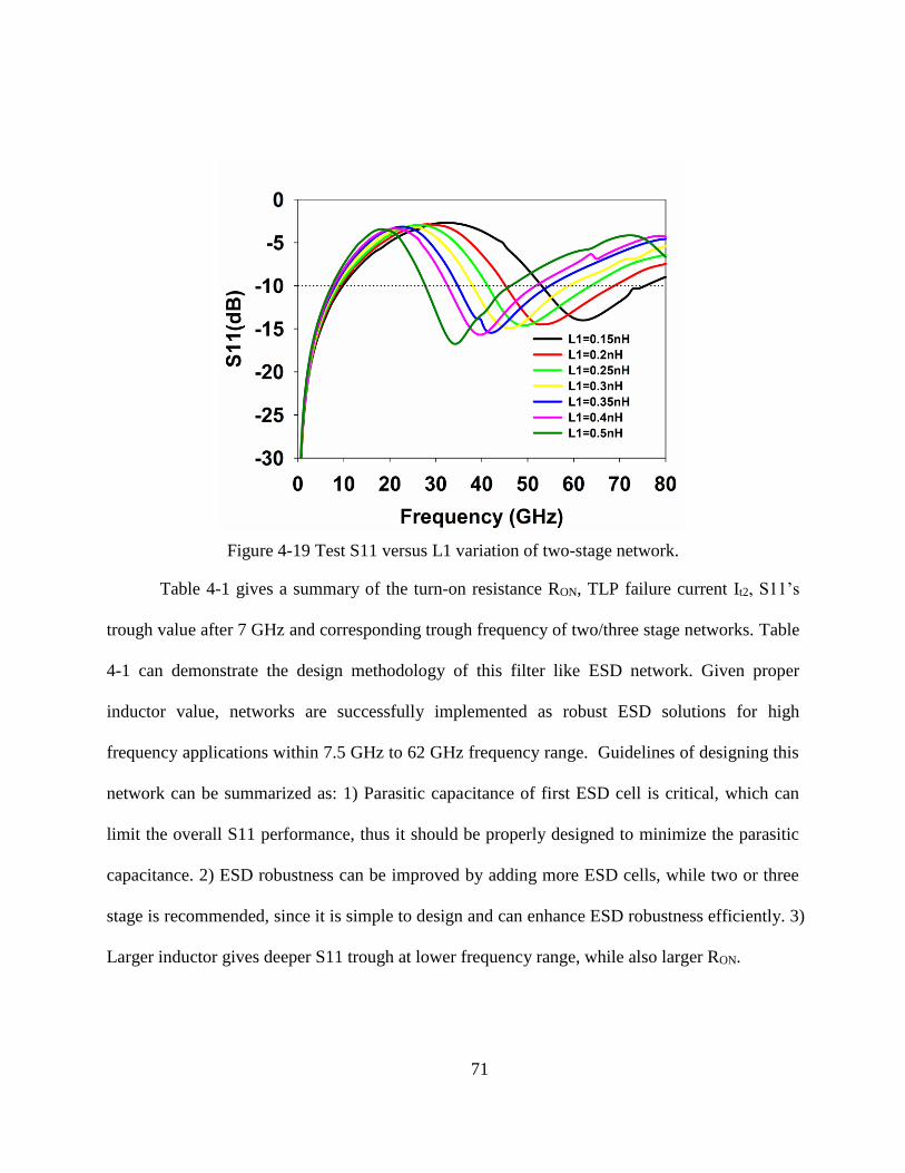
71
Figure 4-19 Test S11 versus L1 variation of two-stage network.
Table 4-1 gives a summary of the turn-on resistance RON, TLP failure current It2, S11’s
trough value after 7 GHz and corresponding trough frequency of two/three stage networks. Table
4-1 can demonstrate the design methodology of this filter like ESD network. Given proper
inductor value, networks are successfully implemented as robust ESD solutions for high
frequency applications within 7.5 GHz to 62 GHz frequency range. Guidelines of designing this
network can be summarized as: 1) Parasitic capacitance of first ESD cell is critical, which can
limit the overall S11 performance, thus it should be properly designed to minimize the parasitic
capacitance. 2) ESD robustness can be improved by adding more ESD cells, while two or three
stage is recommended, since it is simple to design and can enhance ESD robustness efficiently. 3)
Larger inductor gives deeper S11 trough at lower frequency range, while also larger RON.

72
Table 4-1 Summarizations of the TLP (100-ns-wide 10-ns rise-time) and S11 test result of
example networks.
Num
of
Stage
L1
(nH)
L2
(nH) RON(Ω)
TLP
It2 (A)
Trough
Frequency
(Ghz)
Trough
S11
(dB)
2 0.15 -- 3.5 4.3 62 -14
2 0.2 -- 3.5 4.3 52 -14
2 0.25 -- 3.6 4.3 49 -15
2 0.3 -- 3.6 4.3 46 -15
2 0.35 -- 3.7 4.4 42 -15
2 0.4 -- 3.7 4.4 40 -16
2 0.5 -- 3.6 4.5 37 -16
3 0.2 1 4.1 5.9 51 -15
3 0.25 1 4.1 5.9 46 -15
3 0.3 1 4.5 5.9 44 -15
3 0.4 1 4.4 5.9 37 -16
3 0.2 0.1 3.8 5.8 40 -14
3 0.3 0.1 4.3 5.9 37 -16
3 0.4 0.1 4.4 5.9 33 -17
3 0.5 0.1 4.4 5.9 30 -18
3 0.6 0.1 4.4 5.9 27 -19
3 0.7 0.1 4.4 5.8 25 -20
3 0.8 0.1 4.4 5.9 23 -20
3 0.9 0.1 4.4 5.9 22 -21
3 1 0.1 4.4 5.9 21 -21
3 1.5 0.1 4.7 5.9 16 -23
3 2 0.1 5.2 5.9 13 -25
3 3 0.1 5.3 5.9 10 -27
3 5 0.1 5.7 5.4 7.5 -29
4.4 Conclusion
An inductor embedded, filter like ESD network and its design methodology was
proposed and discussed in details. Example designs were given and the results of their S11, TLP
and vfTLP test were compared. Concluding from the data, the proposed ESD networks work

73
well for high frequency I/O protection within 7.5 GHz to 62 GHz frequency range. Guidelines
were provided for further design and optimization.

74
CHAPTER 5 HIGH HOLDING VOLTAGE HETEROGENEOUS
STACKING SCR
5.1 Introduction
Silicon controlled rectifier (SCR) is widely used in electrostatic discharge (ESD)
protection, for its high robustness and less silicon consumption [25, 62]. However, the holding
voltage of SCR device is low, only several volts in most widely used processes, contributing to
deep snapback. As a result, SCR is prone to latch up [25, 63, 64]. To increase the holding voltage,
there are two major approaches, the first is targeting for reducing the minority carrier injection
efficiency of parasitic BJT in single SCR, like adjusting the dimension of doping area between P-
well and N-well in SCR [65], enlarging the space between anode to cathode [66]. Another
approach is stacking the SCR [67], while conventional stacking method usually introducing
affections to triggering performance: increase the trigger voltage along with the holding voltage.
Hence, the depth of snapback has not been optimized in conventional stacking method. To solve
this issue, new stacking methodology is proposed in [68] and successfully reduce the depth of
snapback. While heterogeneous stacking optimization still involves important design tradeoffs.
In this paper, we proposed a heterogeneous stacking structure for latch-up free design, which can
increase the holding voltage and also keep the trigger voltage nearly as same as single SCR
device. DC and TLP characterizations are used to demonstrate the results.

75
5.2 Device Structure
Figure 5-2 show the cross section views of conventional stacking SCR-SCR (CS SCR-
SCR) and proposed stacking SCR-LVTSCR (PS SCR-LVTSCR). The triggering mechanism is
compared in Figure 5-3. In conventional stacking method, SCRs in the first and second stage are
connected in series, therefore the holding and triggering voltages of the structure will be equal to
the sum of holding and triggering voltages in each stage.
Figure 5-1 Cross section view of tradition stacking SCR-SCR (CS SCR-SCR).
Figure 5-2 Cross section view of proposed stacking SCR-LVTSCR (PS SCR-LVTSCR).

76
LVTS
-CR
SCR
Cathode
Anode
RSCR
SCR
Cathode
Anode
Re
sis
tor B
y_
pa
ss
ES
D P
ath
ES
D P
ath
CS SCR-SCR PS SCR-LVTSCR
Figure 5-3 Triggering methodology of conventional and proposed structure.
By contrast, proposed structures add a “resistor by pass” in parallel to second stage,
helping to trigger the entire structure. ESD pulse firstly triggers SCR in first stage, generating a
current on resistor by pass. When the current reach to a certain level, usually 0.1A, the overall
voltage on the resistor (60Ω in our case) will be large enough to trigger the second stage
LVTSCR. This turn on condition can be kept if voltage over anode to cathode are larger than
VHolding-first-stage + VTriggering-second-stage.
To be mentioned, a LVTSCR is used in the second stage in this heterogeneous stacking
structure can be trigger easier than stacking structures using identical SCRs in each stage, since
less effort will be taken to trigger the second stage LVTSCR.

77
5.3 Experimental Results
DC, TLP characterizations are conducted to demonstrate the effectiveness of the
proposed stacking structure. Results are shown in Figure 5-4 to Figure 5-6, separately.
Figure 5-4 DC results of single SCR, CS SCR-SCR and PS SCR-LVTSCR.
DC performance of single SCR, CS SCR-SCR and PS SCR-LVTSCR are compared in
Figure 5-4. The results show that the breakdown voltage of CS SCR-SCR increases to 58.1V,
while for PS SCR-LVTSCR (28.4V), the breakdown voltage is nearly as same as single SCR,
whose breakdown voltage is 27.8V.
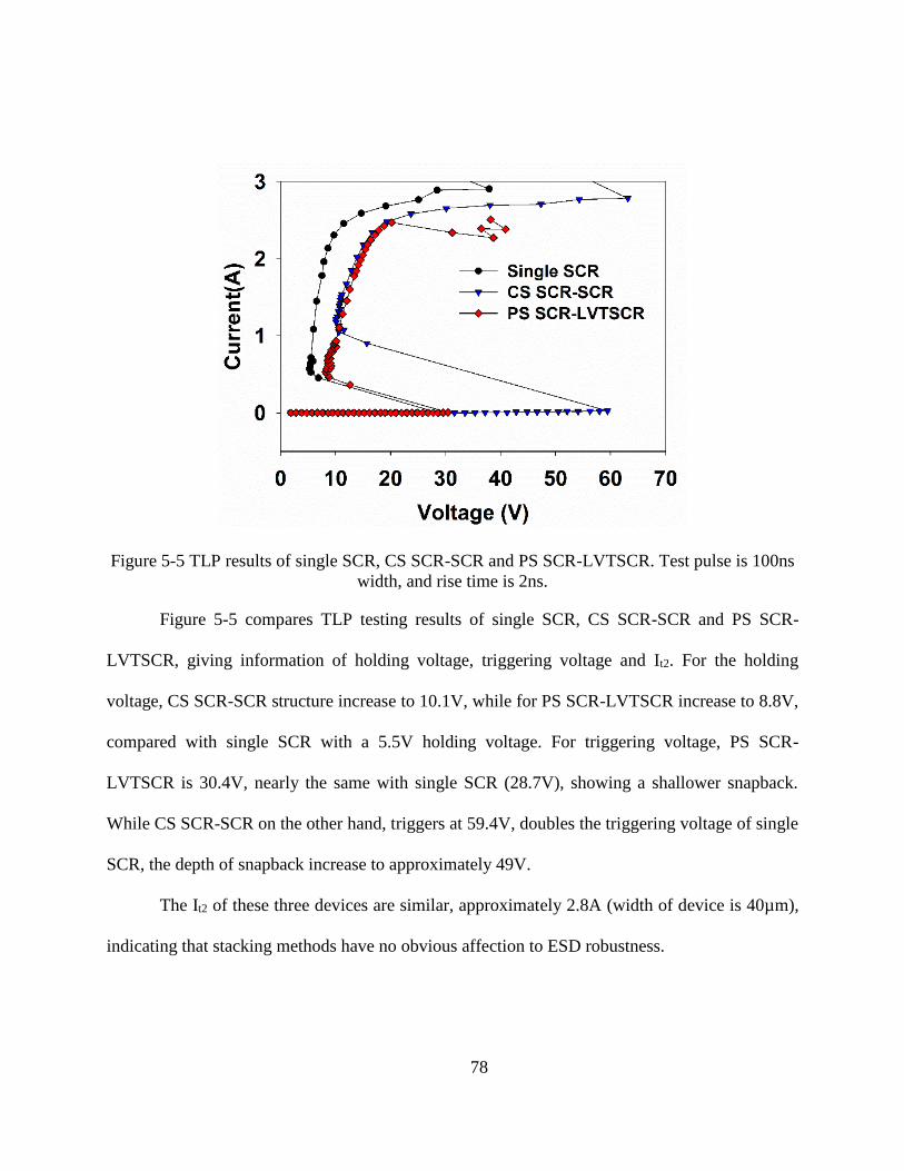
78
Figure 5-5 TLP results of single SCR, CS SCR-SCR and PS SCR-LVTSCR. Test pulse is 100ns
width, and rise time is 2ns.
Figure 5-5 compares TLP testing results of single SCR, CS SCR-SCR and PS SCR-
LVTSCR, giving information of holding voltage, triggering voltage and It2. For the holding
voltage, CS SCR-SCR structure increase to 10.1V, while for PS SCR-LVTSCR increase to 8.8V,
compared with single SCR with a 5.5V holding voltage. For triggering voltage, PS SCR-
LVTSCR is 30.4V, nearly the same with single SCR (28.7V), showing a shallower snapback.
While CS SCR-SCR on the other hand, triggers at 59.4V, doubles the triggering voltage of single
SCR, the depth of snapback increase to approximately 49V.
The It2 of these three devices are similar, approximately 2.8A (width of device is 40µm),
indicating that stacking methods have no obvious affection to ESD robustness.
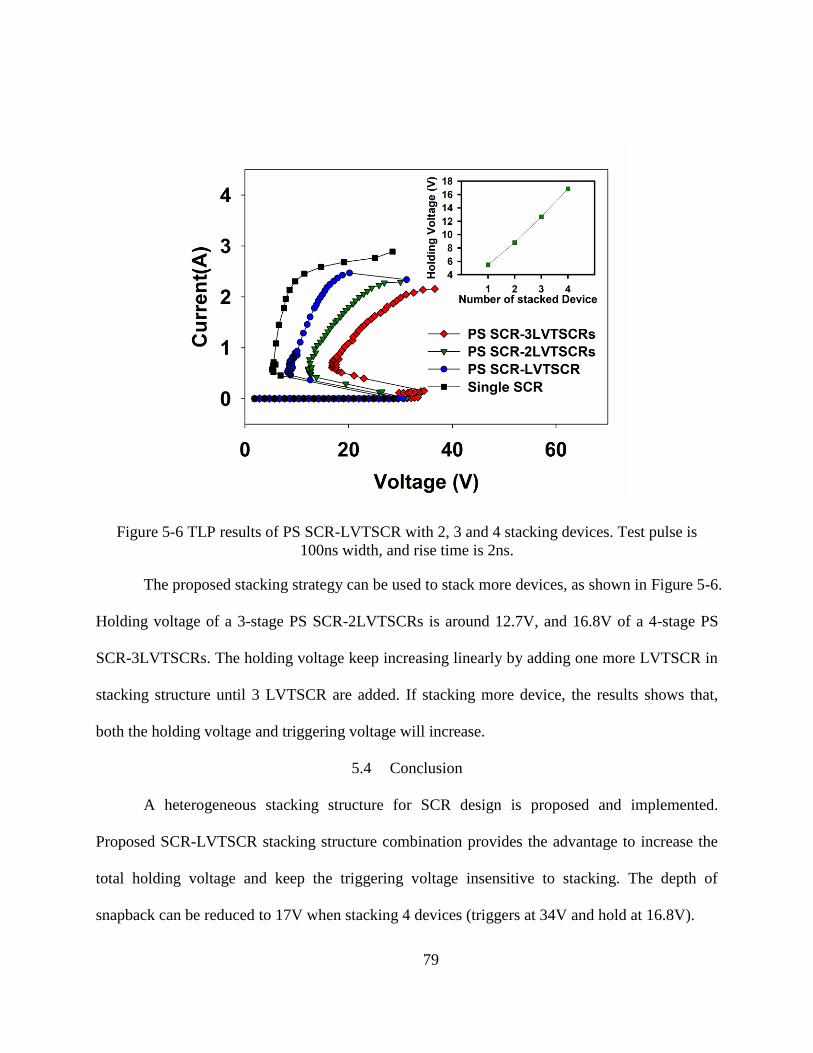
79
Figure 5-6 TLP results of PS SCR-LVTSCR with 2, 3 and 4 stacking devices. Test pulse is
100ns width, and rise time is 2ns.
The proposed stacking strategy can be used to stack more devices, as shown in Figure 5-6.
Holding voltage of a 3-stage PS SCR-2LVTSCRs is around 12.7V, and 16.8V of a 4-stage PS
SCR-3LVTSCRs. The holding voltage keep increasing linearly by adding one more LVTSCR in
stacking structure until 3 LVTSCR are added. If stacking more device, the results shows that,
both the holding voltage and triggering voltage will increase.
5.4 Conclusion
A heterogeneous stacking structure for SCR design is proposed and implemented.
Proposed SCR-LVTSCR stacking structure combination provides the advantage to increase the
total holding voltage and keep the triggering voltage insensitive to stacking. The depth of
snapback can be reduced to 17V when stacking 4 devices (triggers at 34V and hold at 16.8V).
80
CHAPTER 6 SUMMARY AND CONCLUSION
ESD related failure is always a major concern for IC reliability and this is particularly
true in advanced silicon technologies. Besides the concerns of ESD robustness, low parasitic
capacitance requirement is critical to ESD design of high-speed and RF I/Os. This dissertation
starts with the fundamentals of ESD phenomena and existing ESD stress models. Capacitance of
basic ESD devices is also investigated. The major contributions of this dissertation are analyzing
the ESD design window in advanced technologies also introduced multiple efficient ESD
solutions for advanced high-speed and RF I/Os.
ESD design window parameters across 350nm bulk technology to 7nm FinFET
technology were discussed in chapter 2. It is a good reference for ESD design in 14nm/7nm
FinFET technologies. This research indicated that ESD design window based on Vt1 and Vgox is
shrinking drastically with technology scaling down. It shown that the potential of extending ESD
design window by adding series resistance degraded significantly in advanced technology nodes,
since victim FETs can barely handle any ESD current in FinFET technologies. Besides, to meet
CDM protection level for digital design, secondary protection for drivers in 7nm and beyond is
needed as Vgox drops significantly. Moreover, for high-speed designs, one needs to consider
lowering the HBM and CDM level further for FinFET technologies as ESD device capacitance
loading becomes significantly higher while no improvement observed in Vt1 or It2 for FETs.
DD-SCR was proposed in this dissertation in chapter 3 as a solution for optimizing the
capacitance in advanced technologies. The designs have been implemented under 28nm CMOS
technology. By combining the advantages of stacked-diode and SCR, DD-SCR shown
outstanding characteristics, such as low parasitic capacitance, high failure current, low overshoot
81
voltage and small RON. These characteristics make DD-SCR an efficient solution for high speed
I/O protection.
An inductor embedded, filter like ESD network was proposed as a solution for RF I/O
protection in chapter 4. Its design methodology were demonstrated through TLP, vfTLP and S11
test in this dissertation. Given proper inductor value, networks were successfully implemented as
robust ESD solutions for high frequency I/O protection within 7.5 GHz to 62 GHz frequency
range.
A heterogeneous stacking methodology for SCR design was introduced and implemented
in this dissertation in chapter 5. This design provided new views for latch-up free SCR design.
Bypass resister was used in the design to help the triggering of the second and following stages
of the stacking structure. Results demonstrated that proposed design can successfully increase
the total holding voltage and also keep the triggering voltage insensitive to stacking. The depth
of snapback can be reduced to 17V when stacking four devices.
As a summary, a few research works on design and characterization of low capacitance
and robust ESD protection devices in advanced semiconductor technologies were introduced in
this dissertation. This dissertation could be a good reference for future ESD protection design.
82
LIST OF REFERENCES
[1] J. E. Vinson and J. J. Liou, "Electrostatic discharge in semiconductor devices: an
overview," Proceedings of the IEEE, vol. 86, no. 2, pp. 399-420, 1998.
[2] A. Wang, "On-chip ESD protection design: mixed-mode simulation and ESD for
RF/mixed-signal ICs," in BCTM 2003, 2003.
[3] M. Kelly, G. Servais, T. Diep, D. Lin, S. Twerefour, and G. Shah, "A comparison of
electrostatic discharge models and failure signatures for CMOS integrated circuit
devices," in Electrical Overstress/Electrostatic Discharge Symposium Proceedings, 1995,
pp. 175-185.
[4] F. Roger, W. Reinprecht, and R. Minixhofer, "Process variation aware ESD design
window considerations on a 0.18um analog, mixed-signal high voltage technology," in
EOS/ESD Symposium Proceedings, 2011, pp. 1-7.
[5] C. Russ, "ESD issues in advanced CMOS bulk and FinFET technologies: Processing,
protection devices and circuit strategies," Microelectronics Reliability, vol. 48, no. 8, pp.
1403-1411, 2008/08/01/ 2008.
[6] M. D. Ker and C. Y. Lin, "ESD protection consideration in nanoscale CMOS
technology," in 2011 11th IEEE International Conference on Nanotechnology, 2011, pp.
720-723.
[7] V. A. Vashchenko, Shibkov, Andrei, ESD Design for Analog Circuits. Springer Science
& Business Media, 2010.
[8] O. Semenov, H. Sarbishaei, and M. Sachdev, ESD protection device and circuit design
for advanced CMOS technologies. Springer Science & Business Media, 2008.
83
[9] Joint JEDEC/ESDA Standard for Electrostatic Discharge Sensitivity Test - Human Body
Model (HBM) - Component Level, JS-001-2017, 2017.
[10] JEDEC, Recommended ESD Target Levels For HBM/MM Qualification, JEP155A.01,
2012.
[11] "JEDEC, Electrostatic Discharge (ESD) Sensitivity Testing Machine Model (MM),
JESD22-A115C," 2010.
[12] "ESDA/JEDEC Joint Standard for Electrostatic Discharge Sensitivity Testing - Charged
Device Model (CDM) - Device Level, JS-002-2014," 2014.
[13] (2012). Industry Council on ESD Target Level - MM Qualification Issues.
[14] (2017). White Paper 1: A Case for Lowering Componont Level HBM/MM ESD
Specifications and Requirements.
[15] (2012). White Paper 2: A Case for Lowering Component Level CDM ESD Specifications
and Requiements.
[16] A. Z. Wang, On-chip ESD protection for integrated circuits: an IC design perspective.
Springer Science & Business Media, 2006.
[17] Y. Zhou and J. J. Hajjar, "CDM ESD failure modes and VFTLP testing for protection
evaluation," in 2008 9th International Conference on Solid-State and Integrated-Circuit
Technology, 2008, pp. 333-336.
[18] "ESDA, Fundamentals of Electrostatic Discharge - Part 3 - Basic ESD Control
Procedures and Materials," 2014.
[19] S. H. Voldman, ESD Basics From Semiconductor Manufacturing to Product Use. John
Wiley & Sons, 2012.

84
[20] A. Dong, M. Miao, J. J. Liou, J. A. Salcedo, and J. J. Hajjar, "Novel structure embedded
with dual-diodes and silicon controlled rectifier for high speed I/O applications," in 2016
IEEE International Nanoelectronics Conference (INEC), 2016, pp. 1-2.
[21] A. Dong et al., "ESD protection structure with reduced capacitance and overshoot voltage
for high speed interface applications," Microelectronics Reliability, vol. 79, pp. 201-205,
2017/12/01/ 2017.
[22] C. Guang et al., "Characterizing diodes for RF ESD protection," IEEE Electron Device
Letters, vol. 25, no. 5, pp. 323-325, 2004.
[23] W. Weihuai, D. Shurong, Z. Lei, Z. Jie, Y. Zhihui, and L. Zhiwei, "GGNMOS as ESD
protection in different nanometer CMOS process," in 2014 IEEE International
Conference on Electron Devices and Solid-State Circuits, 2014, pp. 1-2.
[24] V. A. Vashchenko, A. Concannon, M. t. Beek, and P. Hopper, "High holding voltage
cascoded LVTSCR structures for 5.5-V tolerant ESD protection clamps," IEEE
Transactions on Device and Materials Reliability, vol. 4, no. 2, pp. 273-280, 2004.
[25] M.-D. Ker and K.-C. Hsu, "Overview of on-chip electrostatic discharge protection design
with SCR-based devices in CMOS integrated circuits," IEEE Transactions on device and
materials reliability, vol. 5, no. 2, pp. 235-249, 2005.
[26] C. Y. Lin and M. D. Ker, "Dual SCR with low-and-constant parasitic capacitance for
ESD protection in 5-GHz RF integrated circuits," in 2010 10th IEEE International
Conference on Solid-State and Integrated Circuit Technology, 2010, pp. 707-709.

85
[27] K. Ming-Dou, "Whole-chip ESD protection design with efficient VDD-to-VSS ESD
clamp circuits for submicron CMOS VLSI," IEEE Transactions on Electron Devices, vol.
46, no. 1, pp. 173-183, 1999.
[28] K. Ming-Dou, W. Chung-Yu, C. Tao, M. J. N. Wu, T. L. Yu, and A. C. Wang, "Whole-
chip ESD protection for CMOS VLSI/ULSI with multiple power pins," in Proceedings of
1994 IEEE International Integrated Reliability Workshop (IRWS), 1994, pp. 124-128.
[29] K. Ming-Dou, "ESD (Electrostatic Discharge) Protection in CMOS Integrated Circuit."
[30] L. He, "Whole Chip ESD Design in CMOS Technology," University of Electronic
Science and Technology of China, 2015.
[31] S. Mitra et al., "I/O Architecture For Improved ESD Protection In Deep Sub-Micron SOI
Technologies," in 2006 IEEE international SOI Conferencee Proceedings, 2006, pp. 37-
38.
[32] G. Boselli, J. Rodriguez, C. Duvvury, and J. Smith, "Analysis of ESD protection
components in 65nm CMOS technology: Scaling perspective and impact on ESD design
window," in 2005 Electrical Overstress/Electrostatic Discharge Symposium, 2005, pp. 1-
10.
[33] J. Li, K. Chatty, R. Gauthier, R. Mishra, and C. Russ, "Technology scaling of advanced
bulk CMOS on-chip ESD protection down to the 32nm node," in 2009 31st EOS/ESD
Symposium, 2009, pp. 1-7.
[34] S. Mitra, R. Gauthier, S. Chang, J. Li, R. Halbach, and C. Seguin, "Maximizing ESD
design window by optimizing gate bias for cascoded drivers in 45nm and beyond SOI

86
technologies," in Electrical Overstress/Electrostatic Discharge Symposium Proceedings
2010, 2010, pp. 1-6.
[35] C. Duvvury, "Embedded Tutorial: Silicon Technology Impact on ESD Qualification," in
2013 26th International Conference on VLSI Design and 2013 12th International
Conference on Embedded Systems, 2013, pp. lxx-lxx.
[36] C. Duvvury, "ESD qualification changes for 45nm and beyond," in 2008 IEEE
International Electron Devices Meeting, 2008, pp. 1-4.
[37] M. P. J. Mergens et al., "Speed optimized diode-triggered SCR (DTSCR) for RF ESD
protection of ultra-sensitive IC nodes in advanced technologies," IEEE Transactions on
Device and Materials Reliability, vol. 5, no. 3, pp. 532-542, 2005.
[38] M. D. Ker, C. Y. Lin, and Y. W. Hsiao, "Overview on ESD Protection Designs of Low-
Parasitic Capacitance for RF ICs in CMOS Technologies," IEEE Transactions on Device
and Materials Reliability, vol. 11, no. 2, pp. 207-218, 2011.
[39] B. J. Huang et al., "Design and Analysis for a 60-GHz Low-Noise Amplifier With RF
ESD Protection," IEEE Transactions on Microwave Theory and Techniques, vol. 57, no.
2, pp. 298-305, 2009.
[40] T. Lim et al., "Generic Electrostatic Discharges Protection Solutions for RF and
Millimeter-Wave Applications," IEEE Transactions on Microwave Theory and
Techniques, vol. 63, no. 11, pp. 3747-3759, 2015.
[41] S. Parthasarathy, J. A. Salcedo, and J. J. Hajjar, "A low leakage poly-gated SCR device
for ESD protection in 65nm CMOS process," in 2013 IEEE International Reliability
Physics Symposium (IRPS), 2013, pp. EL.5.1-EL.5.5.

87
[42] A. Z. H. Wang et al., "A review on RF ESD protection design," IEEE Transactions on
Electron Devices, vol. 52, no. 7, pp. 1304-1311, 2005.
[43] E. Rosenbaum and S. Hyvonen, "On-chip ESD protection for RF I/Os: devices, circuits
and models," in 2005 IEEE International Symposium on Circuits and Systems, 2005, pp.
1202-1205 Vol. 2.
[44] S. Dong, M. Miao, J. Wu, J. Zeng, Z. Liu, and J. J. Liou, "Low-Capacitance SCR
Structure for RF I/O Application," IEEE Transactions on Electromagnetic Compatibility,
vol. 55, no. 2, pp. 241-247, 2013.
[45] J. A. Salcedo, S. Parthasarathy, and J. J. Hajjar, "Monolithic ESD protection for
distributed high speed applications in 28-nm CMOS technology," in 2014 IEEE
International Reliability Physics Symposium, 2014, pp. 4C.3.1-4C.3.4.
[46] Q. Cui, J. A. Salcedo, S. Parthasarathy, Y. Zhou, J. J. Liou, and J. J. Hajjar, "High-
Robustness and Low-Capacitance Silicon-Controlled Rectifier for High-Speed I/O ESD
Protection," IEEE Electron Device Letters, vol. 34, no. 2, pp. 178-180, 2013.
[47] S. Parthasarathy, J. A. Salcedo, and J. J. Hajjar, "Design of SCR devices for SiGe
BiCMOS applications," in 2011 IEEE Bipolar/BiCMOS Circuits and Technology
Meeting, 2011, pp. 235-238.
[48] C. Y. Lin and M. L. Fan, "Optimization on Layout Style of Diode Stackup for On-Chip
ESD Protection," IEEE Transactions on Device and Materials Reliability, vol. 14, no. 2,
pp. 775-777, 2014.

88
[49] F. Ma, Y. Han, S. Dong, L. Zhong, H. Liang, and F. Gao, "Improvement on diode string
structure for 65-nm RF ESD protection," Solid-State Electronics, vol. 89, pp. 142-145,
2013/11/01/ 2013.
[50] C. Y. Lin, M. L. Fan, M. D. Ker, L. W. Chu, J. C. Tseng, and M. H. Song, "Improving
ESD robustness of stacked diodes with embedded SCR for RF applications in 65-nm
CMOS," in 2014 IEEE International Reliability Physics Symposium, 2014, pp. EL.1.1-
EL.1.4.
[51] R. C. Sun, Z. Wang, M. Klebanov, W. Liang, J. J. Liou, and D. G. Liu, "Silicon-
Controlled Rectifier for Electrostatic Discharge Protection Solutions With Minimal
Snapback and Reduced Overshoot Voltage," IEEE Electron Device Letters, vol. 36, no. 5,
pp. 424-426, 2015.
[52] J. J. L. Y. Li, "Evaluation of Transient Behavior of Polysilicon-Bound Diode for Fast
ESD Applications," IEEE Transactions on Electron Devices, vol. 57, no. 10, pp. 2736-
2743, 2010.
[53] Y. Li, J. J. Liou, J. E. Vinson, and L. Zhang, "Investigation of LOCOS- and Polysilicon-
Bound Diodes for Robust Electrostatic Discharge (ESD) Applications," IEEE
Transactions on Electron Devices, vol. 57, no. 4, pp. 814-819, 2010.
[54] S. Galal and B. Razavi, "Broadband ESD protection circuits in CMOS technology," IEEE
Journal of Solid-State Circuits, vol. 38, no. 12, pp. 2334-2340, 2003.
[55] J. T. Chen, C. Y. Lin, and M. D. Ker, "On-Chip ESD Protection Device for High-Speed
I/O Applications in CMOS Technology," IEEE Transactions on Electron Devices, vol.
64, no. 10, pp. 3979-3985, 2017.
89
[56] M. H. Tsai, S. S. H. Hsu, F. L. Hsueh, C. P. Jou, and T. J. Yeh, "A 17.5–26 GHz Low-
Noise Amplifier With Over 8 kV ESD Protection in 65 nm CMOS," IEEE Microwave
and Wireless Components Letters, vol. 22, no. 9, pp. 483-485, 2012.
[57] S. Parthasarathy, R. Carrillo-Ramirez, J. Salcedo, and J. J. Hajjar, "Design of ESD
protection for large signal swing RF inputs operating to 24GHz in 0.18um SiGe BiCMOS
process," in 2015 IEEE Radio Frequency Integrated Circuits Symposium (RFIC), 2015,
pp. 413-416.
[58] C. Y. Lin, L. W. Chu, and M. D. Ker, "ESD Protection Design for 60-GHz LNA With
Inductor-Triggered SCR in 65-nm CMOS Process," IEEE Transactions on Microwave
Theory and Techniques, vol. 60, no. 3, pp. 714-723, 2012.
[59] C. Y. Lin and R. K. Chang, "Design of ESD Protection Device for K/Ka -Band
Applications in Nanoscale CMOS Process," IEEE Transactions on Electron Devices, vol.
62, no. 9, pp. 2824-2829, 2015.
[60] T. Lim, J. Jimenez, P. Benech, J. M. Fournier, and P. Galy, "Transmission line with
integrated symmetrical 1-kV HBM DC - 100 GHz ESD protection in advanced CMOS
technologies," in 2012 42nd European Microwave Conference, 2012, pp. 1162-1165.
[61] F. Farbiz, A. Appaswamy, A. A. Salman, and G. Boselli, "Overshoot-induced failures in
forward-biased diodes: A new challenge to high-speed ESD design," in 2013 IEEE
International Reliability Physics Symposium (IRPS), 2013, pp. 2B.1.1-2B.1.8.
[62] J. A. Salcedo, David Casey, and Graham McCorkell, "Apparatus and method for
protecting electronic circuits.," ed. U.S. Patent: ADI, Inc., 2013.
90
[63] C. T. Wang, T. H. Tang, and K. C. Su, "Latch-up free ESD protection design with SCR
structure in advanced CMOS technology," in 2011 International Reliability Physics
Symposium, 2011, pp. 4C.3.1-4C.3.4.
[64] M. P. J. Mergens, C. C. Russ, K. G. Verhaege, J. Armer, P. C. Jozwiak, and R. Mohn,
"High holding current SCRs (HHI-SCR) for ESD protection and latch-up immune IC
operation," Microelectronics Reliability, vol. 43, no. 7, pp. 993-1000, 2003/07/01/ 2003.
[65] S. Dong, J. Wu, M. Miao, J. Zeng, Y. Han, and J. J. Liou, "High-Holding-Voltage
Silicon-Controlled Rectifier for ESD Applications," IEEE Electron Device Letters, vol.
33, no. 10, pp. 1345-1347, 2012.
[66] A. Chatterjee, J. Seitchik, and P. Yang, "A Simple Holding Voltage Analysis for Latchup
in Epitaxial CMOS," in 1986 Symposium on VLSI Technology. Digest of Technical
Papers, 1986, pp. 25-26.
[67] Z. Liu, J. J. Liou, S. Dong, and Y. Han, "Silicon-Controlled Rectifier Stacking Structure
for High-Voltage ESD Protection Applications," IEEE Electron Device Letters, vol. 31,
no. 8, pp. 845-847, 2010.
[68] F. Ma et al., "High Holding Voltage SCR-LDMOS Stacking Structure With Ring-
Resistance-Triggered Technique," IEEE Electron Device Letters, vol. 34, no. 9, pp. 1178-
1180, 2013.