Design of High-Voltage Switch-Mode Power Amplifier Based on ...
10
Research Article Design of High-Voltage Switch-Mode Power Amplifier Based on Digital-Controlled Hybrid Multilevel Converter Yanbin Hou, Wanrong Sun, Aifeng Ren, and Shuming Liu School of Electronic Engineering, Xidian University, Xi’an 710071, China Correspondence should be addressed to Yanbin Hou; [email protected] Received 20 April 2016; Revised 18 August 2016; Accepted 25 August 2016 Academic Editor: Wei-Zen Chen Copyright © 2016 Yanbin Hou et al. is is an open access article distributed under the Creative Commons Attribution License, which permits unrestricted use, distribution, and reproduction in any medium, provided the original work is properly cited. Compared with conventional Class-A, Class-B, and Class-AB amplifiers, Class-D amplifier, also known as switching amplifier, employs pulse width modulation (PWM) technology and solid-state switching devices, capable of achieving much higher efficiency. However, PWM-based switching amplifier is usually designed for low-voltage application, offering a maximum output voltage of several hundred Volts. erefore, a step-up transformer is indispensably adopted in PWM-based Class-D amplifier to produce high- voltage output. In this paper, a switching amplifier without step-up transformer is developed based on digital pulse step modulation (PSM) and hybrid multilevel converter. Under the control of input signal, cascaded power converters with separate DC sources operate in PSM switch mode to directly generate high-voltage and high-power output. e relevant topological structure, operating principle, and design scheme are introduced. Finally, a prototype system is built, which can provide power up to 1400 Watts and peak voltage up to ±1700 Volts. And the performance, including efficiency, linearity, and distortion, is evaluated by experimental tests. 1. Introduction Class-A, Class-B, and Class-AB amplifiers are usually termed as linear amplifiers for their switching devices operate in linear mode, while Class-D amplifiers are also known as switching amplifiers, in which the switching devices are either fully turned on or completely turned off, operating in switch mode. is means that when the switch is conducting (turned on) there is virtually no voltage across the switch and that when the switch is not conducting (turned off) there is no current flowing through the switch. So the ideal efficiency of Class-D amplifier is 100% in theory [1]. In fact, the commonly used semiconductor switching devices, such as IGBT (Insulated Gate Bipolar Transistor) and MOSFET (Metal Oxide Semiconductor Field Effect Transistor), have saturation voltage drop or on-state resistance when they are turned on. Although part of power has been consumed as heat by switches, efficiencies over 85% can be achieved in most situations for Class-D amplifier. By comparison, linear amplifier has a theoretical efficiency of 78% at the utmost [2]. In a typical Class-D amplifier, input signal is converted into a series of pulses through pulse width modulation (PWM), which serve as control signals for driving power switches. e switching devices together with DC sources realize power and voltage amplification. At the output stage of Class-D amplifier, low-frequency amplified signal is retrieved across the load by filtering out high-frequency carrier wave. Due to its single half-bridge or full-bridge topology, PWM- based switching amplifier usually outputs a peak voltage of dozens or hundreds of Volts [3]. Step-up transformer seems to be a ready-made solution to boost up output voltage, since existing PWM-based switching amplifiers can provide enough output power. However, the noisy and heavy midfrequency step-up transformer will make the whole amplifier system bulky and expensive. What is worse, the insertion of step-up transformer between amplifier and load will introduce additional power loss, thus reducing the overall system efficiency. One of our outside partners is confronted with such a dilemma. ey built an analog PWM-based switching amplifier and used a bulky step-up transformer to produce the rated voltage of 1000 Volts and rated power of 1000 Watts across a 1000-Ohm resistor over the operating frequency range of 100–1000 Hertz. But the average system efficiency is about 70%, presenting a challenge to cool. What Hindawi Publishing Corporation Active and Passive Electronic Components Volume 2016, Article ID 3982594, 9 pages http://dx.doi.org/10.1155/2016/3982594
Transcript of Design of High-Voltage Switch-Mode Power Amplifier Based on ...
Research ArticleDesign of High-Voltage Switch-Mode Power Amplifier Based onDigital-Controlled Hybrid Multilevel Converter
Yanbin Hou Wanrong Sun Aifeng Ren and Shuming Liu
School of Electronic Engineering Xidian University Xirsquoan 710071 China
Correspondence should be addressed to Yanbin Hou ybhoumailxidianeducn
Received 20 April 2016 Revised 18 August 2016 Accepted 25 August 2016
Academic Editor Wei-Zen Chen
Copyright copy 2016 Yanbin Hou et al This is an open access article distributed under the Creative Commons Attribution Licensewhich permits unrestricted use distribution and reproduction in any medium provided the original work is properly cited
Compared with conventional Class-A Class-B and Class-AB amplifiers Class-D amplifier also known as switching amplifieremploys pulse widthmodulation (PWM) technology and solid-state switching devices capable of achievingmuch higher efficiencyHowever PWM-based switching amplifier is usually designed for low-voltage application offering a maximum output voltage ofseveral hundredVoltsTherefore a step-up transformer is indispensably adopted in PWM-basedClass-D amplifier to produce high-voltage output In this paper a switching amplifier without step-up transformer is developed based on digital pulse stepmodulation(PSM) and hybrid multilevel converter Under the control of input signal cascaded power converters with separate DC sourcesoperate in PSM switchmode to directly generate high-voltage and high-power outputThe relevant topological structure operatingprinciple and design scheme are introduced Finally a prototype system is built which can provide power up to 1400 Watts andpeak voltage up to plusmn1700 Volts And the performance including efficiency linearity and distortion is evaluated by experimentaltests
1 Introduction
Class-A Class-B and Class-AB amplifiers are usually termedas linear amplifiers for their switching devices operate inlinear mode while Class-D amplifiers are also known asswitching amplifiers in which the switching devices areeither fully turned on or completely turned off operating inswitch mode This means that when the switch is conducting(turned on) there is virtually no voltage across the switchand that when the switch is not conducting (turned off)there is no current flowing through the switch So the idealefficiency of Class-D amplifier is 100 in theory [1] In factthe commonly used semiconductor switching devices suchas IGBT (Insulated Gate Bipolar Transistor) and MOSFET(Metal Oxide Semiconductor Field Effect Transistor) havesaturation voltage drop or on-state resistance when they areturned on Although part of power has been consumed asheat by switches efficiencies over 85 can be achieved inmost situations for Class-D amplifier By comparison linearamplifier has a theoretical efficiency of 78 at the utmost [2]
In a typical Class-D amplifier input signal is convertedinto a series of pulses through pulse width modulation
(PWM) which serve as control signals for driving powerswitches The switching devices together with DC sourcesrealize power and voltage amplification At the output stage ofClass-D amplifier low-frequency amplified signal is retrievedacross the load by filtering out high-frequency carrier waveDue to its single half-bridge or full-bridge topology PWM-based switching amplifier usually outputs a peak voltageof dozens or hundreds of Volts [3] Step-up transformerseems to be a ready-made solution to boost up outputvoltage since existing PWM-based switching amplifiers canprovide enough output power However the noisy and heavymidfrequency step-up transformer will make the wholeamplifier system bulky and expensive What is worse theinsertion of step-up transformer between amplifier and loadwill introduce additional power loss thus reducing the overallsystem efficiency One of our outside partners is confrontedwith such a dilemma They built an analog PWM-basedswitching amplifier and used a bulky step-up transformer toproduce the rated voltage of 1000 Volts and rated power of1000 Watts across a 1000-Ohm resistor over the operatingfrequency range of 100ndash1000 Hertz But the average systemefficiency is about 70 presenting a challenge to cool What
Hindawi Publishing CorporationActive and Passive Electronic ComponentsVolume 2016 Article ID 3982594 9 pageshttpdxdoiorg10115520163982594
2 Active and Passive Electronic Components
Signalpreproc
PSMmodulator
Multilevelpower
converterFull
bridgeSwitching
signals
Control unit
LPF
Hybrid converter unit
Parameters setting
Status monitoring and control
Auxiliary unit
ADC
Power source unit
Electronic Electric
G(ain)
Ui Uo = GUi
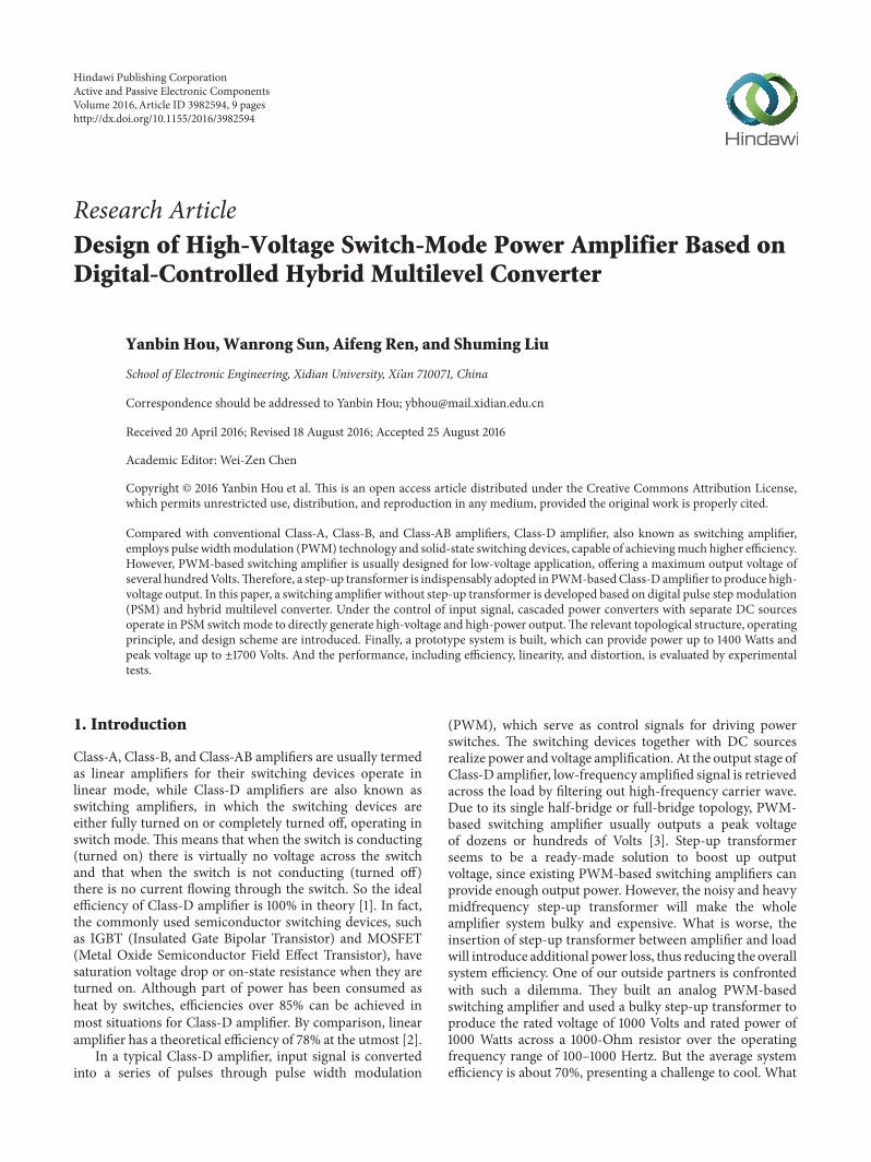
Figure 1 Block diagram of high-voltage switching amplifier
is more the bulky step-up transformer has a weight of over 50kilograms almost two-thirds of the gross weight Our targetis to rebuild a switching amplifier with main requirements asfollows
Output voltage up to 1000VrmsOutput power up to 1000WOverall efficiency above 85Output distortion below 25Gross weight less than 80Kg
The requirements about high efficiency and light weightexclude the possibility of using step-up transformer to boostup voltage From the view of power electronics the desiredswitching amplifier can be considered as a programmablehigh-voltage power supply operating in switch mode underthe control of input signal NPC- (neutral point clamped-)based and cascaded H-bridge (full-bridge) multilevel con-verters are two commonly used topologies to directly producehigh-voltage output [4 5] The former uses a single high-voltage DC source and multiple cascaded semiconductorswitches together with clamping diodes or flying capacitorsusually involving complicated voltage balancing measures[6ndash8] The latter adopts modular design of which eachconverter consists of a low-voltage DC source and four semi-conductor switches Thus it will demand a great number ofsemiconductor switches and control signals when employingmultiple cascaded full-bridge converters to generate high-voltage output
In order to directly generate high-voltage output andreduce power semiconductor switches as well a new circuitarchitecture called hybrid multilevel converter is proposedin this paper The corresponding control scheme is designedon the basis of pulse step modulation (PSM) by adoptingdigital signal processing technology Section 2 introduces thedesign scheme Section 3 gives the performance tests and
Section 4 is the conclusion Experimental results show thatthis new system can provide up to 1400Watts and plusmn1700Voltspeak voltage with high efficiency and low distortion asexpected
2 Design of High-Voltage Switching Amplifier
Figure 1 shows the functional block diagram of high-voltageswitch-mode power amplifier developed in this paper
As shown in Figure 1 this switching amplifier consistsof four units which are control unit hybrid converter unitpower source unit and auxiliary unit respectively Theworkflow is as follows
Small analog input signal is firstly preprocessed and thendigitalized by a 12-bit analog-to-digital converter (ADC)According to the ADC data and user settings PSM modu-lator generates a set of switching signals which are furtherisolated and driven before applying to hybrid converterunit Under the control of corresponding switching signalsmultilevel power converter transforms energy from separatelow-voltage DC sources to augment modulated switchingsignals and full bridge takes charge of the switchover betweenpositive and negative phase At the final output stage a low-pass filter is used to retrieve the expected amplified outputwaveform
For the sake of efficiency and reliability the whole systemwas developed utilizing digital signal processing technologyPSM modulator was implemented with a high-performancefloating-point digital signal processor (DSP) and a high-volume field programmable gate array (FPGA) Auxiliaryunit adopted digital technologies at the most extent likehuman-machine interface (HMI) for setting gain and otherparameters measuring output voltage and current monitor-ing temperatures and so on
The following sections introduce key points in detail todevelop a plusmn1700Vp1400W switch-mode power amplifier of
Active and Passive Electronic Components 3
+
+
+
+
+
L
RC
D2
D1
D3
D4
S1
S2
S3
S4
minus
minus
minus
minus
minusUs
Us
Us
Us
Uo
(a)t0
S3 lsquolsquoSMrsquorsquo
S2 lsquolsquoSMrsquorsquo
S1 lsquolsquoSMrsquorsquo
S4 lsquolsquoPWMrsquorsquo4
3
2
Us
Us
Us
Us
Uo
(b)
Figure 2 PSM-based HVPS (a) Schematic and (b) principle
which efficiency is expected to be no less than 85 with lowdistortion in the midfrequency range (100ndash1000Hz)
21 Pulse Step Modulation Brown Boveri Corporation pre-sented pulse step modulation (PSM) and applied it broadlyin short-wave transmitter and high-voltage power supply(HVPS) [9ndash11] Figure 2 illustrates the schematic circuit andwork principle of PSM-based HVPS to quadruple its outputvoltage of each converter
As shown in Figure 2(a) a PSM-based HVPS basicallyconsists of multiple (four in this example) power convertersconnected in series which work in switch mode underthe control of input reference signal (here taking semi-sinewave as an example) Each power converter has a separatelow-voltage DC source 119880s a semiconductor switch S anda free-wheeling diode D [12] The diode is to provide alow impedance path when the corresponding converter isswitched off allowing current from other working convertersto pass through Regardless of voltage drops across diodesand switches total output voltage 119880o is simply equal toseveral times of unit step voltage 119880s depending on thenumber of switched-on power inverters Obviously actualoutput voltage is just a roughly stepwise approximation to theexpected waveform which is referred to as step modulation(SM) To further refine output pulse width modulation(PWM) and LC components are adopted to smooth thetransition from one step to the other Taking Figure 2(a) asan example let switches S1simS3 operate in SM mode and letswitch S4 operate in PWM mode the filtered output voltage119880o across the load is plotted as a blue solid line in Figure 2(b)
As stated above PSM consists of coarse SM and finePWM Figure 2(b) shows that each SM operates at a ratherlow frequency the same as input reference signal It is alsonoticed that PWM need to switch much faster than SMto achieve an accurate representation of the input signalFollowing Nyquist theorem PWM need to run at least twicethe maximum input frequency but actual design generally
adopts a much higher ratio (typically 10 to 50) for reducingdistortion [13] In theory high-frequency PWM can improveoutput waveformHowever switch loss increases as switchingbecomes faster Generally PWM will take a compromisebetween output waveform and switch loss depending on thepractical application
22 Hybrid Converter Unit As illustrated in Figure 2 PSM-based HVPS can only produce unipolar voltage In order tooperate as an amplifier circuit needs to be further modifiedConventional method is that every converter adopts full-bridge architecture employing four switches and two groupsswitching signals to produce 0simplusmn119880s However it will increasesystem cost and control complexity if many full-bridgeconverters are used to produce high voltage
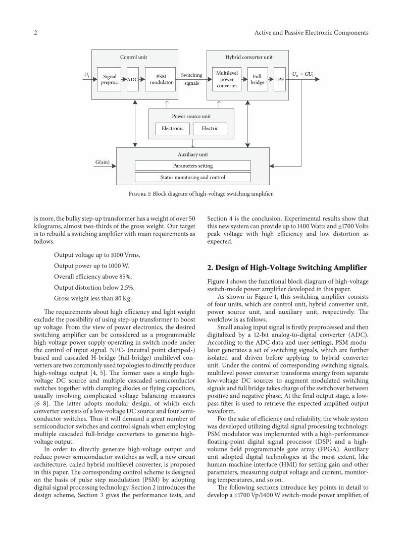
In this paper a hybrid multilevel converter was designedin which information on amplitude and phase of input signalis separately modulated As shown in Figure 3 eight cascadedpower converters (PC1simPC8) produce desired amplitudewhile full bridge (composed of Q1simQ4) controls phaseCompared with cascaded full-bridge converters this hybridarchitecture employs much fewer switches and control sig-nals
Power converters PC1simPC8 are identical except for cor-responding to different switching signals Each one consistsof separated 220V3A DC source 119880s semiconductor switchS and free-wheeling diode D In consideration of switchingspeed and power loss semiconductor switches S1simS8 all usepower MOSFETs which have small on-state resistance Free-wheeling diodes D1simD8 adopt fast recovery diodes Intensivesimulations and tests confirm that MOSFET and diode sufferthe maximum potential difference of 119880s in all situations somany powerMOSFETs available can be used such as IRF8402SK1507 and FMV11N60E 2SK1507 with a typical drain-source on-state resistance of 119877DS(on) = 085Ω was adoptedDiodes adopted MUR860 with a maximum instantaneousforward voltage drop 119881F = 15 V Switches S1simS7 and S8 are
4 Active and Passive Electronic Components
PC1
PC2
S1D1
asymp
S2D2
asymp
S8D8
R
PC8
Q1
Q3
Q2
Q4
+
L
C
+
minus
Phase
Phase
Phase
Phase
minus
a
b
c d
SM1
SM2
PWM
+minus
+minus
+minus
Us
Us
Us
Uo
Figure 3 Schematic of hybrid multilevel converter
under the control of switching signals SM1simSM7 and PWMrespectively
The full bridge is built with four discrete IGBTs Q1simQ4under the control of switching signals Phase+Phaseminus Whenthe input signal is nonnegative Q2 and Q3 are switchedoff simultaneously meanwhile Q1 and Q4 are switched onsimultaneously and vice versa Although ZVS (Zero VoltageSwitching) is applied dead time is also inserted betweencommutations to avoid potential shoot-through risk IGBTsadopted IXYS IXBH12N300 with a maximum saturationvoltage drop 119881CE(sat) = 32V
Inductor 119871 capacitor 119862 and resistive load 119877 make upa Butterworth low-pass filter (LPF) to recover the amplifiedoutput signal from high-voltage modulated waveform Givenload resistance and cut-off frequency inductance and capac-itance can be obtained by
119871 =119877
(radic2120587119891119862)
119862 =1
(2radic2120587119877119891119862)
(1)
where 119891119862 denotes the cut-off frequency 119891119862 in Hertz 119871 inHenrys 119862 in Faradays and 119877 in Ohms respectively
The LPF filter has a minus3 dB cut-off frequency of 5 kHzcorresponding to 119877 = 1 kΩ 119871 = 44mH and 119862 = 18 nF
23 Digital PSMModulator Unlike carrier-based PWM thatadopts analog modulation [14] we designed digital PSM
modulator to generate SM and PWM switching signals by thefollowing formula
119872(119899) = fix(1198661003816100381610038161003816119880i (119899)1003816100381610038161003816
119880s)
119889 (119899) = rem(1198661003816100381610038161003816119880i (119899)1003816100381610038161003816
119880s)
Phase+ = ON if 119880i (119899) ge 0OFF if 119880i (119899) lt 0
Phaseminus =
ON if 119880i (119899) lt 0
OFF if 119880i (119899) ge 0
119899 = 1199051 1199052 119905119899
(2)
where |119880i(119899)| is the absolute amplitude of sampled inputsignal at moment 119905119899 119866 is predefined voltage gain 119880s is DCsource voltage Function fix(sdot) rounds the data towards zeroresulting in an integer119872(119899) which is the number of powerconverters switched on between 119905119899 and 119905119899+1 Function rem(sdot)retrieves the remainder after division so 119889(119899) is a decimalrepresenting the ldquoonrdquo time of a power converter relative tosampling interval that is 119889(119899) determines the duty cycle ofPWMswitching signal (eg 050 is equal to 50) Phase+ andPhaseminus record the phase information about sampled inputsignal serving as the switching signals for full bridge
In other words during sampling interval between 119905119899 and119905119899+1 119872(119899) power converters work in SM mode and onepower converter operates in PWM mode with a duty cycleof 119889(119899) Obviously the switching frequency of PWM is equal
Active and Passive Electronic Components 5
to the sampling frequency of ADCHere we adopted unipolarcentre-aligned PWMwhose advantages and implementationcould be referred to [15]
24 Software Simulation The workflow of the above switch-ing amplifier is demonstrated through simulation For exam-ple a sine wave of 1 kHz and plusmn1 Vp needs to be amplifiedby a voltage gain of 119866 = 800 It is assumed that samplingfrequency of ADC is 40 kSas so that there will be 40 sampledpoints in a cycle as shown in Figure 4(a) According to (2)if 119880s = 220Vdc it needs that three converters work in SMmode and one converter operates in PWM mode DigitalPSM modulator generates switching signals as plotted inFigure 4(b) The unused converters are always switched offwhich are not plotted in Figure 4(b) Figure 4(c) gives themodulated amplitude after amplification measured betweenpoints a and b (marked in Figure 3) Figure 4(d) shows theoutput voltages after adding phase information and filteringmeasured between points c and d (marked in Figure 3) inwhich the blue solid line represents modulated waveformafter amplification and the red dotted line is the final outputvoltage across load after LPF demodulation
In this simulation zero-crossing points of input signal areall sampled by ADC However this may be not true in mostactual situations So ZVS will be applied to force all SM andPWM signals to be off at the moments of commutation forexample when 119905 = 05 10 15 and 20ms in Figure 4(b)
It is important to note that IGBTs usually take more timeto be switched on or off compared to MOSFETs due to finiteswitching speed In order to protect full bridge at themomentof voltage phase alternation proper dead time is added toensure that short circuit will not happen between points a andb (marked in Figure 3) which means that both phase controlsignals in Figure 4(b) are switched off during the dead time
3 Experimental Tests and Results
31 Prototype System Based on the above introduction ahigh-voltage switch-mode power amplifier is developed asshown in Figure 5
From top to down there are main distribution boxelectronic case for control unit and auxiliary unit electriccase for hybrid converter unit and two 4-channel AC-DC220V power sources in a 19-inch standard cabinet (600mmtimes 600mm times 1050mm W times D timesH) A resistor of 1000Ohmswith cooling equipment is used as dummy load laid outsidethe cabinet for facilitating heat dissipation
32 Total Harmonic Distortion Many factors in switchingamplifier can cause distortion such as power switchesnonlinearity of output LPF DC source voltage fluctuationsdead time and modulation technologies As one of the mostcommon and important features total harmonic distortion(THD) is usually used to evaluate system distortion Giventhat input signal is a sine wave THD is most commonlydefined as the ratio of the rms amplitude of a set of harmonic
0
1
0 05 10 15 20(ms)
minus1
sin (2120587ft)
Ui
(V)
(a)
SM1On
On
On
On
On
On
SM2
SM3
PWM
Phase+
Phaseminus
Off
Off
Off
Off
Off
Off0 05 10 15 20
(ms)
(b)
0 05 10 15 20(ms)
0220440660880
Uab
(V)
(c)
0 05 10 15 20(ms)
UnfilteredFiltered
minus880
minus440
0
440
880
Ucd
(V)
(d)
Figure 4 Simulation of switching power amplifier (a) Sampledinput signal (b) switching signals for power converters and fullbridge and ((c) and (d)) voltage waveforms measured between a-b and c-d points respectively (points a-d marked in Figure 3)
frequencies to that of fundamental frequency which can beformulated as follows [16]
THD =radic11988022+ 11988032+ sdot sdot sdot + 119880119899
2
1198801
(3)
where 1198801 denotes the rms voltage of fundamental frequencyand 119880119899 is the rms voltage of the 119899th harmonic frequency
Sine wave of 1 Vrms with frequency sweeping from 100 to1000Hz was used as input signal to investigate the prototypesystem Figure 6 shows the screenshots of output waveforms
6 Active and Passive Electronic Components
Table 1 THD values of power amplifier system
Freq (Hz) Output power (W)300 650 960 1300
100 152 147 106 104200 159 153 112 105300 165 152 115 104400 173 158 123 105500 168 158 126 109600 169 160 127 119800 171 166 133 1301000 177 176 140 134
Figure 5 Photo of power amplifier system
at frequencies of 100 500 and 1000Hz On the oscilloscopedisplay the upper channel shows output voltage and the lowerone is its corresponding fast Fourier transform (FFT) It isnoticed that the FFT spectrum is plotted as magnitude in dBrelative to 1 Vrms the corresponding rms voltage is retrievedby
119880119899 = 1011988911986111989920 (4)
where 119889119861119899 denotes the voltage gain relative to 1 Vrms at the119899th harmonic frequency and 119880119899 is the rms output voltage ofthe 119899th harmonic frequency
Table 1 lists THD valuesmeasured at four different outputpower values Without regard to individual measurementerrors it can be found that THD value increases as signal fre-quency rises and that THD value decreases as output powerincreases It is not difficult to explain this phenomenonWithinput signal sweeping from low frequency to high frequencythe sampled points in a single cycle reduce resulting inoutput waveform not so smooth as before When outputpower increases signal-to-noise ratio is improved to a certaindegree
It is noticed that measured output power in Table 1 is anaverage of output power valuesmeasured from 100 to 1000Hzwith a step size of 100Hz keeping input signal amplitude
Table 2 Efficiency of power amplifier system
119875c (W) 119875o (W) Efficiency350 300 857712 650 9131022 960 9391361 1300 955
constant Averaging is aimed at diminishing measurementerror for high voltage A typical example is shown in Figure 6With the same input signal and amplification gain peakand rms output voltages fluctuated irregularly at differentfrequencies
33TheMaximumOutput Tomeasure themaximumoutputpower sine wave of 1 kHz is used as input signal and itsamplitude increases until output distortion reaches THD =10 Figure 7 shows output voltage when amplifier outputsthe maximum power of about 1500W
As shown in Figure 7 waveform appears apparent clip-ping at the maximum output power value For the sakeof practicability the maximum output voltage is limited to3400Vpp (a critical point of appearing voltage clipping) andthe corresponding maximum output power is hence loweredto about 1400W estimated by
119875o =1
8119877
119880pp2=1
8 times 1000
times (3400V)2 = 1445Watts (5)
34 Efficiency and Linearity The efficiency corresponding tothe output power in Table 1 is listed in Table 2 119875c representsthe whole power consumed by entire amplifier system 119875o isthe output power measured on load It is noticed that 119875o is anaverage of output power valuesmeasured from 100 to 1000Hzwith a step size of 100Hz as the same reason explained inSection 32
As for an amplifier nonlinearity caused by gain variationwill affect the waveform shape of analog output with respectto the corresponding analog input Figure 8 plots three groupsof output versus input signal amplitude with a constantvoltage gain of 119866 = 1000
As shown in Figure 8 the output approximately followsa linear relationship relative to the input The average voltagegains measured at frequencies of 400 800 and 1000Hz are1027 1036 and 1021 respectively That is to say this newdeveloped high-voltage switch-mode power amplifier has astatistical linearity error less than 4
35 Automatic Protection The running status of poweramplifier system is under real-time surveillance includingoutput voltage output current output power and systemtemperature Once any alarm about overvoltage overcurrentor overtemperature is triggered amplifier system will beshut down within 1ms as illustrated in Figure 9 In theoscilloscope screenshot Channel 1 records alarm signal andChannel 2 is recording switching signal If a failure occursfalling edge of alarm signal is first detected and low level
Active and Passive Electronic Components 7
(a) (b)
(c)
Figure 6 Oscilloscope screenshots of output voltage at frequencies of (a) 100Hz (500Vdiv 2msdiv) (b) 500Hz (500Vdiv 500 usdiv)and (c) 1000Hz (500Vdiv 200 usdiv)
Figure 7 High-voltage output waveform of clipping with THD =10 (1 kVdiv 200 usdiv)
of alarm signal is then reconfirmed within about 600 us Iffailure does happen control unit will switch off all powerconverters one by one within 40 us
36 Overall Comparison Table 3 gives an overall comparisonbetween the new digital PSM-based switching amplifier andthe existing analog PWM-based switching amplifier The
400 Hz800 Hz1000 Hz
3500
3000
2500
2000
1500
1000
500
012 14 16 18 20 22 24 26 28 30 32 34
Input signal amplitude (Vpp)
Out
put v
olta
ge (V
pp)
fi =
fi =
fi =
Figure 8 Linearity of power amplifier system
specification and performance of the latter are providedby our partner off campus including modulation technol-ogy circuit topology output voltage and power distortion
8 Active and Passive Electronic Components
(a) (b)
Figure 9 Oscilloscope screenshots of automatic protection (a) CH1 failure alarm signal and CH2 first closed SM1 signal (b) CH1 failurealarm and CH2 last closed PWM signal (2Vdiv 200 usdiv)
efficiency and weight For convenience the two switchingamplifiers are labelled as PSM-based amplifier and PWM-based amplifier respectively
In PWM-based switching amplifier a high-speed analogcomparator compares a triangular carrier wave of 300KHzwith the input signal to generate PWMswitching signals Butin PSM-based switching amplifier as described in Section 24the corresponding PWM switching signal is 40KHz HighPWM switching frequency means that more sampled pointsare used to approximate the input signal thus yieldingsmooth waveform and low distortion Furthermore PWM-based switching amplifier only adopts fast power MOSFETsin the half-bridge stage while PSM-based switching amplifieradopts IGBTs with much higher blocking voltage in thefull-bridge stage But IGBT switches slower than MOSFETdue to tail-current effect at turn-off Therefore PWM-basedswitching amplifier can generate better output waveformHowever the dependence of PWM-based amplifier on step-up transformer lowers overall efficiency and increases grossweight
4 Conclusion
In this paper a switch-mode power amplifier based on digitalpulse step modulation and hybrid multilevel converter isdesigned to directly produce high-voltage output without theaid of step-up transformer
Compared with available PWM-based switching ampli-fier coupled with a step-up transformer this new developedsystem can provide output power up to 1400 Watts and peakvoltage up to plusmn1700 Volts with encouraging efficiency andportability The major advantages are its hybrid architectureand digital modulation When directly generating high-voltage output a lot of control signals and power switches arecut down by modulating the information on amplitude andphase of input signal separately
However there is further work to improve this design
Table 3 Comparisons of two power amplifier systems
Items PSM-based amplifier PWM-based amplifierModulation Digital PSM Analog PWMCircuit topology Multilevel Half bridgePower supplies DC 220V DC plusmn80VStep-up transformer No need Need
Maximum output plusmn1700Vp plusmn1500Vp1400W 1200W
THDlowast 138 085Efficiencylowast 942 825Gross weight 50Kg 80KgUser interface Touch LCD LED indicatorslowastThe test condition is outputting 1000Vrms sine at 1 KHz
Firstly switching frequency needs to be increased formore practical applications However MOSFETs in high-voltage converter cannot switch at a frequency as high(300 kHz or above) as they do in PWM-based audio amplifierbecause this will lead to serious overshoot and EMI problemsThus more elaborate modulation scheme needs to be consid-ered such as phase-shifting modulation technologies
Secondly more intelligent strategies should be adoptedFor example redundant power converters can timely replacethe failed ones without shutdown If there is no usable powerconverter amplifier will appropriately lower output voltage toprevent serious distortion
Competing Interests
The authors declare that there are no competing interestsregarding the publication of this paper
Acknowledgments
This research is supported by the Fundamental ResearchFunds for the Central Universities under Grant no JB140205
Active and Passive Electronic Components 9
References
[1] M Bloechl M Bataineh and D Harrell ldquoClass D switchingpower amplifiers theory design and performancerdquo in Proceed-ings of the IEEE SoutheastCon 2004 pp 123ndash146 GreensboroNC USA March 2004
[2] M Berkhout and L Dooper ldquoClass-D audio amplifiers inmobile applicationsrdquo IEEETransactions onCircuits and Systemsvol 57 no 5 pp 992ndash1002 2010
[3] D Self Audio Power Amplifier Design Handbook Focal PressBoston Mass USA 5th edition 2009
[4] F J Liu Modern Inverter Technology and Application Pub-lishing House of Electronics Industry Beijing China 2006(Chinese)
[5] V Sala R Salehi M Moreno-Eguilaz M Salehifar and LRomeral ldquoClamping diode caused distortion in multilevelNPC Full-Bridge audio power amplifiersrdquo in Proceedings of the38th Annual Conference on IEEE Industrial Electronics Society(IECON rsquo12) pp 4941ndash4948 IEEE Montreal Canada October2012
[6] W W He P Palmer X Q Zhang M Snook and Z H WangldquoIGBT series connection under active voltage controlrdquo in Pro-ceedings of the 14th European Conference on Power Electronicsand Applications (EPE rsquo11) pp 1ndash9 IEEE Birmingham UKSeptember 2011
[7] P Palmer W W He X Q Zhang J Zhang and M SnookldquoIGBT series connection under Active Voltage Control withtemporary clamprdquo in Proceedings of the 38th Annual Conferenceon IEEE Industrial Electronics Society (IECON rsquo12) pp 465ndash470Montreal Canada October 2012
[8] T Lu Z M Zhao S Q Ji et al ldquoDesign of voltage balancingcontrol circuit for series connected HV-IGBTsrdquo in Proceedingsof the 16th International Conference on Electrical Machines andSystems (ICEMS rsquo13) pp 515ndash518 IEEE Busan South KoreaOctober 2013
[9] W Schminke ldquoThe merits of modern technology for todayrsquoshigh power short-wave transmittersrdquo IEEE Transactions onBroadcasting vol 34 no 2 pp 126ndash133 1988
[10] J Alex and W Schminke ldquoA high voltage power supply fornegative ion NBI based on PSM technologyrdquo in Proceedings ofthe 17th IEEENPSS Symposium on Fusion Engineering (SOFErsquo97) vol 2 pp 1063ndash1066 IEEE SanDiego Calif USAOctober1997
[11] L Y Yao Y Q Wang X H Mao Y L Wang and Q Li ldquoAfully digital controller of high-voltage power supply for ECRHsystem on HL-2Ardquo IEEE Transactions on Plasma Science vol40 no 3 pp 793ndash797 2012
[12] J Alex andW Schminke ldquoFast switchingmodular high-voltageDCAC-power supplies for RF-amplifiers and other applica-tionsrdquo in Proceedings of the 16th IEEENPSS Symposium onFusion Engineering (SOFE rsquo95) pp 936ndash939 IEEE ChampaignIll USA October 1995
[13] M J Hawksford ldquoModulation and system techniques in PWMand SDMswitching amplifiersrdquo Journal of theAudio EngineeringSociety vol 54 no 3 pp 107ndash139 2006
[14] M H Rashid Power Electronics HandbookmdashDevices Cir-cuits andApplications Butterworth-Heinemann BostonMassUSA 3rd edition 2011
[15] B Lei G-C Xiao and X-L Wu ldquoComparison of performancebetween bipolar and unipolar double-frequency sinusoidalpulse width modulation in a digitally controlled H-bridge
inverter systemrdquo Chinese Physics B vol 22 no 6 Article ID060509 pp 281ndash288 2013
[16] D Shmilovitz ldquoOn the definition of total harmonic distortionand its effect on measurement interpretationrdquo IEEE Transac-tions on Power Delivery vol 20 no 1 pp 526ndash528 2005
International Journal of
AerospaceEngineeringHindawi Publishing Corporationhttpwwwhindawicom Volume 2014
RoboticsJournal of
Hindawi Publishing Corporationhttpwwwhindawicom Volume 2014
Hindawi Publishing Corporationhttpwwwhindawicom Volume 2014
Active and Passive Electronic Components
Control Scienceand Engineering
Journal of
Hindawi Publishing Corporationhttpwwwhindawicom Volume 2014
International Journal of
RotatingMachinery
Hindawi Publishing Corporationhttpwwwhindawicom Volume 2014
Hindawi Publishing Corporation httpwwwhindawicom
Journal ofEngineeringVolume 2014
Submit your manuscripts athttpwwwhindawicom
VLSI Design
Hindawi Publishing Corporationhttpwwwhindawicom Volume 2014
Hindawi Publishing Corporationhttpwwwhindawicom Volume 2014
Shock and Vibration
Hindawi Publishing Corporationhttpwwwhindawicom Volume 2014
Civil EngineeringAdvances in
Acoustics and VibrationAdvances in
Hindawi Publishing Corporationhttpwwwhindawicom Volume 2014
Hindawi Publishing Corporationhttpwwwhindawicom Volume 2014
Electrical and Computer Engineering
Journal of
Advances inOptoElectronics
Hindawi Publishing Corporation httpwwwhindawicom
Volume 2014
The Scientific World JournalHindawi Publishing Corporation httpwwwhindawicom Volume 2014
SensorsJournal of
Hindawi Publishing Corporationhttpwwwhindawicom Volume 2014
Modelling amp Simulation in EngineeringHindawi Publishing Corporation httpwwwhindawicom Volume 2014
Hindawi Publishing Corporationhttpwwwhindawicom Volume 2014
Chemical EngineeringInternational Journal of Antennas and
Propagation
International Journal of
Hindawi Publishing Corporationhttpwwwhindawicom Volume 2014
Hindawi Publishing Corporationhttpwwwhindawicom Volume 2014
Navigation and Observation
International Journal of
Hindawi Publishing Corporationhttpwwwhindawicom Volume 2014
DistributedSensor Networks
International Journal of
2 Active and Passive Electronic Components
Signalpreproc
PSMmodulator
Multilevelpower
converterFull
bridgeSwitching
signals
Control unit
LPF
Hybrid converter unit
Parameters setting
Status monitoring and control
Auxiliary unit
ADC
Power source unit
Electronic Electric
G(ain)
Ui Uo = GUi
Figure 1 Block diagram of high-voltage switching amplifier
is more the bulky step-up transformer has a weight of over 50kilograms almost two-thirds of the gross weight Our targetis to rebuild a switching amplifier with main requirements asfollows
Output voltage up to 1000VrmsOutput power up to 1000WOverall efficiency above 85Output distortion below 25Gross weight less than 80Kg
The requirements about high efficiency and light weightexclude the possibility of using step-up transformer to boostup voltage From the view of power electronics the desiredswitching amplifier can be considered as a programmablehigh-voltage power supply operating in switch mode underthe control of input signal NPC- (neutral point clamped-)based and cascaded H-bridge (full-bridge) multilevel con-verters are two commonly used topologies to directly producehigh-voltage output [4 5] The former uses a single high-voltage DC source and multiple cascaded semiconductorswitches together with clamping diodes or flying capacitorsusually involving complicated voltage balancing measures[6ndash8] The latter adopts modular design of which eachconverter consists of a low-voltage DC source and four semi-conductor switches Thus it will demand a great number ofsemiconductor switches and control signals when employingmultiple cascaded full-bridge converters to generate high-voltage output
In order to directly generate high-voltage output andreduce power semiconductor switches as well a new circuitarchitecture called hybrid multilevel converter is proposedin this paper The corresponding control scheme is designedon the basis of pulse step modulation (PSM) by adoptingdigital signal processing technology Section 2 introduces thedesign scheme Section 3 gives the performance tests and
Section 4 is the conclusion Experimental results show thatthis new system can provide up to 1400Watts and plusmn1700Voltspeak voltage with high efficiency and low distortion asexpected
2 Design of High-Voltage Switching Amplifier
Figure 1 shows the functional block diagram of high-voltageswitch-mode power amplifier developed in this paper
As shown in Figure 1 this switching amplifier consistsof four units which are control unit hybrid converter unitpower source unit and auxiliary unit respectively Theworkflow is as follows
Small analog input signal is firstly preprocessed and thendigitalized by a 12-bit analog-to-digital converter (ADC)According to the ADC data and user settings PSM modu-lator generates a set of switching signals which are furtherisolated and driven before applying to hybrid converterunit Under the control of corresponding switching signalsmultilevel power converter transforms energy from separatelow-voltage DC sources to augment modulated switchingsignals and full bridge takes charge of the switchover betweenpositive and negative phase At the final output stage a low-pass filter is used to retrieve the expected amplified outputwaveform
For the sake of efficiency and reliability the whole systemwas developed utilizing digital signal processing technologyPSM modulator was implemented with a high-performancefloating-point digital signal processor (DSP) and a high-volume field programmable gate array (FPGA) Auxiliaryunit adopted digital technologies at the most extent likehuman-machine interface (HMI) for setting gain and otherparameters measuring output voltage and current monitor-ing temperatures and so on
The following sections introduce key points in detail todevelop a plusmn1700Vp1400W switch-mode power amplifier of
Active and Passive Electronic Components 3
+
+
+
+
+
L
RC
D2
D1
D3
D4
S1
S2
S3
S4
minus
minus
minus
minus
minusUs
Us
Us
Us
Uo
(a)t0
S3 lsquolsquoSMrsquorsquo
S2 lsquolsquoSMrsquorsquo
S1 lsquolsquoSMrsquorsquo
S4 lsquolsquoPWMrsquorsquo4
3
2
Us
Us
Us
Us
Uo
(b)
Figure 2 PSM-based HVPS (a) Schematic and (b) principle
which efficiency is expected to be no less than 85 with lowdistortion in the midfrequency range (100ndash1000Hz)
21 Pulse Step Modulation Brown Boveri Corporation pre-sented pulse step modulation (PSM) and applied it broadlyin short-wave transmitter and high-voltage power supply(HVPS) [9ndash11] Figure 2 illustrates the schematic circuit andwork principle of PSM-based HVPS to quadruple its outputvoltage of each converter
As shown in Figure 2(a) a PSM-based HVPS basicallyconsists of multiple (four in this example) power convertersconnected in series which work in switch mode underthe control of input reference signal (here taking semi-sinewave as an example) Each power converter has a separatelow-voltage DC source 119880s a semiconductor switch S anda free-wheeling diode D [12] The diode is to provide alow impedance path when the corresponding converter isswitched off allowing current from other working convertersto pass through Regardless of voltage drops across diodesand switches total output voltage 119880o is simply equal toseveral times of unit step voltage 119880s depending on thenumber of switched-on power inverters Obviously actualoutput voltage is just a roughly stepwise approximation to theexpected waveform which is referred to as step modulation(SM) To further refine output pulse width modulation(PWM) and LC components are adopted to smooth thetransition from one step to the other Taking Figure 2(a) asan example let switches S1simS3 operate in SM mode and letswitch S4 operate in PWM mode the filtered output voltage119880o across the load is plotted as a blue solid line in Figure 2(b)
As stated above PSM consists of coarse SM and finePWM Figure 2(b) shows that each SM operates at a ratherlow frequency the same as input reference signal It is alsonoticed that PWM need to switch much faster than SMto achieve an accurate representation of the input signalFollowing Nyquist theorem PWM need to run at least twicethe maximum input frequency but actual design generally
adopts a much higher ratio (typically 10 to 50) for reducingdistortion [13] In theory high-frequency PWM can improveoutput waveformHowever switch loss increases as switchingbecomes faster Generally PWM will take a compromisebetween output waveform and switch loss depending on thepractical application
22 Hybrid Converter Unit As illustrated in Figure 2 PSM-based HVPS can only produce unipolar voltage In order tooperate as an amplifier circuit needs to be further modifiedConventional method is that every converter adopts full-bridge architecture employing four switches and two groupsswitching signals to produce 0simplusmn119880s However it will increasesystem cost and control complexity if many full-bridgeconverters are used to produce high voltage
In this paper a hybrid multilevel converter was designedin which information on amplitude and phase of input signalis separately modulated As shown in Figure 3 eight cascadedpower converters (PC1simPC8) produce desired amplitudewhile full bridge (composed of Q1simQ4) controls phaseCompared with cascaded full-bridge converters this hybridarchitecture employs much fewer switches and control sig-nals
Power converters PC1simPC8 are identical except for cor-responding to different switching signals Each one consistsof separated 220V3A DC source 119880s semiconductor switchS and free-wheeling diode D In consideration of switchingspeed and power loss semiconductor switches S1simS8 all usepower MOSFETs which have small on-state resistance Free-wheeling diodes D1simD8 adopt fast recovery diodes Intensivesimulations and tests confirm that MOSFET and diode sufferthe maximum potential difference of 119880s in all situations somany powerMOSFETs available can be used such as IRF8402SK1507 and FMV11N60E 2SK1507 with a typical drain-source on-state resistance of 119877DS(on) = 085Ω was adoptedDiodes adopted MUR860 with a maximum instantaneousforward voltage drop 119881F = 15 V Switches S1simS7 and S8 are
4 Active and Passive Electronic Components
PC1
PC2
S1D1
asymp
S2D2
asymp
S8D8
R
PC8
Q1
Q3
Q2
Q4
+
L
C
+
minus
Phase
Phase
Phase
Phase
minus
a
b
c d
SM1
SM2
PWM
+minus
+minus
+minus
Us
Us
Us
Uo
Figure 3 Schematic of hybrid multilevel converter
under the control of switching signals SM1simSM7 and PWMrespectively
The full bridge is built with four discrete IGBTs Q1simQ4under the control of switching signals Phase+Phaseminus Whenthe input signal is nonnegative Q2 and Q3 are switchedoff simultaneously meanwhile Q1 and Q4 are switched onsimultaneously and vice versa Although ZVS (Zero VoltageSwitching) is applied dead time is also inserted betweencommutations to avoid potential shoot-through risk IGBTsadopted IXYS IXBH12N300 with a maximum saturationvoltage drop 119881CE(sat) = 32V
Inductor 119871 capacitor 119862 and resistive load 119877 make upa Butterworth low-pass filter (LPF) to recover the amplifiedoutput signal from high-voltage modulated waveform Givenload resistance and cut-off frequency inductance and capac-itance can be obtained by
119871 =119877
(radic2120587119891119862)
119862 =1
(2radic2120587119877119891119862)
(1)
where 119891119862 denotes the cut-off frequency 119891119862 in Hertz 119871 inHenrys 119862 in Faradays and 119877 in Ohms respectively
The LPF filter has a minus3 dB cut-off frequency of 5 kHzcorresponding to 119877 = 1 kΩ 119871 = 44mH and 119862 = 18 nF
23 Digital PSMModulator Unlike carrier-based PWM thatadopts analog modulation [14] we designed digital PSM
modulator to generate SM and PWM switching signals by thefollowing formula
119872(119899) = fix(1198661003816100381610038161003816119880i (119899)1003816100381610038161003816
119880s)
119889 (119899) = rem(1198661003816100381610038161003816119880i (119899)1003816100381610038161003816
119880s)
Phase+ = ON if 119880i (119899) ge 0OFF if 119880i (119899) lt 0
Phaseminus =
ON if 119880i (119899) lt 0
OFF if 119880i (119899) ge 0
119899 = 1199051 1199052 119905119899
(2)
where |119880i(119899)| is the absolute amplitude of sampled inputsignal at moment 119905119899 119866 is predefined voltage gain 119880s is DCsource voltage Function fix(sdot) rounds the data towards zeroresulting in an integer119872(119899) which is the number of powerconverters switched on between 119905119899 and 119905119899+1 Function rem(sdot)retrieves the remainder after division so 119889(119899) is a decimalrepresenting the ldquoonrdquo time of a power converter relative tosampling interval that is 119889(119899) determines the duty cycle ofPWMswitching signal (eg 050 is equal to 50) Phase+ andPhaseminus record the phase information about sampled inputsignal serving as the switching signals for full bridge
In other words during sampling interval between 119905119899 and119905119899+1 119872(119899) power converters work in SM mode and onepower converter operates in PWM mode with a duty cycleof 119889(119899) Obviously the switching frequency of PWM is equal
Active and Passive Electronic Components 5
to the sampling frequency of ADCHere we adopted unipolarcentre-aligned PWMwhose advantages and implementationcould be referred to [15]
24 Software Simulation The workflow of the above switch-ing amplifier is demonstrated through simulation For exam-ple a sine wave of 1 kHz and plusmn1 Vp needs to be amplifiedby a voltage gain of 119866 = 800 It is assumed that samplingfrequency of ADC is 40 kSas so that there will be 40 sampledpoints in a cycle as shown in Figure 4(a) According to (2)if 119880s = 220Vdc it needs that three converters work in SMmode and one converter operates in PWM mode DigitalPSM modulator generates switching signals as plotted inFigure 4(b) The unused converters are always switched offwhich are not plotted in Figure 4(b) Figure 4(c) gives themodulated amplitude after amplification measured betweenpoints a and b (marked in Figure 3) Figure 4(d) shows theoutput voltages after adding phase information and filteringmeasured between points c and d (marked in Figure 3) inwhich the blue solid line represents modulated waveformafter amplification and the red dotted line is the final outputvoltage across load after LPF demodulation
In this simulation zero-crossing points of input signal areall sampled by ADC However this may be not true in mostactual situations So ZVS will be applied to force all SM andPWM signals to be off at the moments of commutation forexample when 119905 = 05 10 15 and 20ms in Figure 4(b)
It is important to note that IGBTs usually take more timeto be switched on or off compared to MOSFETs due to finiteswitching speed In order to protect full bridge at themomentof voltage phase alternation proper dead time is added toensure that short circuit will not happen between points a andb (marked in Figure 3) which means that both phase controlsignals in Figure 4(b) are switched off during the dead time
3 Experimental Tests and Results
31 Prototype System Based on the above introduction ahigh-voltage switch-mode power amplifier is developed asshown in Figure 5
From top to down there are main distribution boxelectronic case for control unit and auxiliary unit electriccase for hybrid converter unit and two 4-channel AC-DC220V power sources in a 19-inch standard cabinet (600mmtimes 600mm times 1050mm W times D timesH) A resistor of 1000Ohmswith cooling equipment is used as dummy load laid outsidethe cabinet for facilitating heat dissipation
32 Total Harmonic Distortion Many factors in switchingamplifier can cause distortion such as power switchesnonlinearity of output LPF DC source voltage fluctuationsdead time and modulation technologies As one of the mostcommon and important features total harmonic distortion(THD) is usually used to evaluate system distortion Giventhat input signal is a sine wave THD is most commonlydefined as the ratio of the rms amplitude of a set of harmonic
0
1
0 05 10 15 20(ms)
minus1
sin (2120587ft)
Ui
(V)
(a)
SM1On
On
On
On
On
On
SM2
SM3
PWM
Phase+
Phaseminus
Off
Off
Off
Off
Off
Off0 05 10 15 20
(ms)
(b)
0 05 10 15 20(ms)
0220440660880
Uab
(V)
(c)
0 05 10 15 20(ms)
UnfilteredFiltered
minus880
minus440
0
440
880
Ucd
(V)
(d)
Figure 4 Simulation of switching power amplifier (a) Sampledinput signal (b) switching signals for power converters and fullbridge and ((c) and (d)) voltage waveforms measured between a-b and c-d points respectively (points a-d marked in Figure 3)
frequencies to that of fundamental frequency which can beformulated as follows [16]
THD =radic11988022+ 11988032+ sdot sdot sdot + 119880119899
2
1198801
(3)
where 1198801 denotes the rms voltage of fundamental frequencyand 119880119899 is the rms voltage of the 119899th harmonic frequency
Sine wave of 1 Vrms with frequency sweeping from 100 to1000Hz was used as input signal to investigate the prototypesystem Figure 6 shows the screenshots of output waveforms
6 Active and Passive Electronic Components
Table 1 THD values of power amplifier system
Freq (Hz) Output power (W)300 650 960 1300
100 152 147 106 104200 159 153 112 105300 165 152 115 104400 173 158 123 105500 168 158 126 109600 169 160 127 119800 171 166 133 1301000 177 176 140 134
Figure 5 Photo of power amplifier system
at frequencies of 100 500 and 1000Hz On the oscilloscopedisplay the upper channel shows output voltage and the lowerone is its corresponding fast Fourier transform (FFT) It isnoticed that the FFT spectrum is plotted as magnitude in dBrelative to 1 Vrms the corresponding rms voltage is retrievedby
119880119899 = 1011988911986111989920 (4)
where 119889119861119899 denotes the voltage gain relative to 1 Vrms at the119899th harmonic frequency and 119880119899 is the rms output voltage ofthe 119899th harmonic frequency
Table 1 lists THD valuesmeasured at four different outputpower values Without regard to individual measurementerrors it can be found that THD value increases as signal fre-quency rises and that THD value decreases as output powerincreases It is not difficult to explain this phenomenonWithinput signal sweeping from low frequency to high frequencythe sampled points in a single cycle reduce resulting inoutput waveform not so smooth as before When outputpower increases signal-to-noise ratio is improved to a certaindegree
It is noticed that measured output power in Table 1 is anaverage of output power valuesmeasured from 100 to 1000Hzwith a step size of 100Hz keeping input signal amplitude
Table 2 Efficiency of power amplifier system
119875c (W) 119875o (W) Efficiency350 300 857712 650 9131022 960 9391361 1300 955
constant Averaging is aimed at diminishing measurementerror for high voltage A typical example is shown in Figure 6With the same input signal and amplification gain peakand rms output voltages fluctuated irregularly at differentfrequencies
33TheMaximumOutput Tomeasure themaximumoutputpower sine wave of 1 kHz is used as input signal and itsamplitude increases until output distortion reaches THD =10 Figure 7 shows output voltage when amplifier outputsthe maximum power of about 1500W
As shown in Figure 7 waveform appears apparent clip-ping at the maximum output power value For the sakeof practicability the maximum output voltage is limited to3400Vpp (a critical point of appearing voltage clipping) andthe corresponding maximum output power is hence loweredto about 1400W estimated by
119875o =1
8119877
119880pp2=1
8 times 1000
times (3400V)2 = 1445Watts (5)
34 Efficiency and Linearity The efficiency corresponding tothe output power in Table 1 is listed in Table 2 119875c representsthe whole power consumed by entire amplifier system 119875o isthe output power measured on load It is noticed that 119875o is anaverage of output power valuesmeasured from 100 to 1000Hzwith a step size of 100Hz as the same reason explained inSection 32
As for an amplifier nonlinearity caused by gain variationwill affect the waveform shape of analog output with respectto the corresponding analog input Figure 8 plots three groupsof output versus input signal amplitude with a constantvoltage gain of 119866 = 1000
As shown in Figure 8 the output approximately followsa linear relationship relative to the input The average voltagegains measured at frequencies of 400 800 and 1000Hz are1027 1036 and 1021 respectively That is to say this newdeveloped high-voltage switch-mode power amplifier has astatistical linearity error less than 4
35 Automatic Protection The running status of poweramplifier system is under real-time surveillance includingoutput voltage output current output power and systemtemperature Once any alarm about overvoltage overcurrentor overtemperature is triggered amplifier system will beshut down within 1ms as illustrated in Figure 9 In theoscilloscope screenshot Channel 1 records alarm signal andChannel 2 is recording switching signal If a failure occursfalling edge of alarm signal is first detected and low level
Active and Passive Electronic Components 7
(a) (b)
(c)
Figure 6 Oscilloscope screenshots of output voltage at frequencies of (a) 100Hz (500Vdiv 2msdiv) (b) 500Hz (500Vdiv 500 usdiv)and (c) 1000Hz (500Vdiv 200 usdiv)
Figure 7 High-voltage output waveform of clipping with THD =10 (1 kVdiv 200 usdiv)
of alarm signal is then reconfirmed within about 600 us Iffailure does happen control unit will switch off all powerconverters one by one within 40 us
36 Overall Comparison Table 3 gives an overall comparisonbetween the new digital PSM-based switching amplifier andthe existing analog PWM-based switching amplifier The
400 Hz800 Hz1000 Hz
3500
3000
2500
2000
1500
1000
500
012 14 16 18 20 22 24 26 28 30 32 34
Input signal amplitude (Vpp)
Out
put v
olta
ge (V
pp)
fi =
fi =
fi =
Figure 8 Linearity of power amplifier system
specification and performance of the latter are providedby our partner off campus including modulation technol-ogy circuit topology output voltage and power distortion
8 Active and Passive Electronic Components
(a) (b)
Figure 9 Oscilloscope screenshots of automatic protection (a) CH1 failure alarm signal and CH2 first closed SM1 signal (b) CH1 failurealarm and CH2 last closed PWM signal (2Vdiv 200 usdiv)
efficiency and weight For convenience the two switchingamplifiers are labelled as PSM-based amplifier and PWM-based amplifier respectively
In PWM-based switching amplifier a high-speed analogcomparator compares a triangular carrier wave of 300KHzwith the input signal to generate PWMswitching signals Butin PSM-based switching amplifier as described in Section 24the corresponding PWM switching signal is 40KHz HighPWM switching frequency means that more sampled pointsare used to approximate the input signal thus yieldingsmooth waveform and low distortion Furthermore PWM-based switching amplifier only adopts fast power MOSFETsin the half-bridge stage while PSM-based switching amplifieradopts IGBTs with much higher blocking voltage in thefull-bridge stage But IGBT switches slower than MOSFETdue to tail-current effect at turn-off Therefore PWM-basedswitching amplifier can generate better output waveformHowever the dependence of PWM-based amplifier on step-up transformer lowers overall efficiency and increases grossweight
4 Conclusion
In this paper a switch-mode power amplifier based on digitalpulse step modulation and hybrid multilevel converter isdesigned to directly produce high-voltage output without theaid of step-up transformer
Compared with available PWM-based switching ampli-fier coupled with a step-up transformer this new developedsystem can provide output power up to 1400 Watts and peakvoltage up to plusmn1700 Volts with encouraging efficiency andportability The major advantages are its hybrid architectureand digital modulation When directly generating high-voltage output a lot of control signals and power switches arecut down by modulating the information on amplitude andphase of input signal separately
However there is further work to improve this design
Table 3 Comparisons of two power amplifier systems
Items PSM-based amplifier PWM-based amplifierModulation Digital PSM Analog PWMCircuit topology Multilevel Half bridgePower supplies DC 220V DC plusmn80VStep-up transformer No need Need
Maximum output plusmn1700Vp plusmn1500Vp1400W 1200W
THDlowast 138 085Efficiencylowast 942 825Gross weight 50Kg 80KgUser interface Touch LCD LED indicatorslowastThe test condition is outputting 1000Vrms sine at 1 KHz
Firstly switching frequency needs to be increased formore practical applications However MOSFETs in high-voltage converter cannot switch at a frequency as high(300 kHz or above) as they do in PWM-based audio amplifierbecause this will lead to serious overshoot and EMI problemsThus more elaborate modulation scheme needs to be consid-ered such as phase-shifting modulation technologies
Secondly more intelligent strategies should be adoptedFor example redundant power converters can timely replacethe failed ones without shutdown If there is no usable powerconverter amplifier will appropriately lower output voltage toprevent serious distortion
Competing Interests
The authors declare that there are no competing interestsregarding the publication of this paper
Acknowledgments
This research is supported by the Fundamental ResearchFunds for the Central Universities under Grant no JB140205
Active and Passive Electronic Components 9
References
[1] M Bloechl M Bataineh and D Harrell ldquoClass D switchingpower amplifiers theory design and performancerdquo in Proceed-ings of the IEEE SoutheastCon 2004 pp 123ndash146 GreensboroNC USA March 2004
[2] M Berkhout and L Dooper ldquoClass-D audio amplifiers inmobile applicationsrdquo IEEETransactions onCircuits and Systemsvol 57 no 5 pp 992ndash1002 2010
[3] D Self Audio Power Amplifier Design Handbook Focal PressBoston Mass USA 5th edition 2009
[4] F J Liu Modern Inverter Technology and Application Pub-lishing House of Electronics Industry Beijing China 2006(Chinese)
[5] V Sala R Salehi M Moreno-Eguilaz M Salehifar and LRomeral ldquoClamping diode caused distortion in multilevelNPC Full-Bridge audio power amplifiersrdquo in Proceedings of the38th Annual Conference on IEEE Industrial Electronics Society(IECON rsquo12) pp 4941ndash4948 IEEE Montreal Canada October2012
[6] W W He P Palmer X Q Zhang M Snook and Z H WangldquoIGBT series connection under active voltage controlrdquo in Pro-ceedings of the 14th European Conference on Power Electronicsand Applications (EPE rsquo11) pp 1ndash9 IEEE Birmingham UKSeptember 2011
[7] P Palmer W W He X Q Zhang J Zhang and M SnookldquoIGBT series connection under Active Voltage Control withtemporary clamprdquo in Proceedings of the 38th Annual Conferenceon IEEE Industrial Electronics Society (IECON rsquo12) pp 465ndash470Montreal Canada October 2012
[8] T Lu Z M Zhao S Q Ji et al ldquoDesign of voltage balancingcontrol circuit for series connected HV-IGBTsrdquo in Proceedingsof the 16th International Conference on Electrical Machines andSystems (ICEMS rsquo13) pp 515ndash518 IEEE Busan South KoreaOctober 2013
[9] W Schminke ldquoThe merits of modern technology for todayrsquoshigh power short-wave transmittersrdquo IEEE Transactions onBroadcasting vol 34 no 2 pp 126ndash133 1988
[10] J Alex and W Schminke ldquoA high voltage power supply fornegative ion NBI based on PSM technologyrdquo in Proceedings ofthe 17th IEEENPSS Symposium on Fusion Engineering (SOFErsquo97) vol 2 pp 1063ndash1066 IEEE SanDiego Calif USAOctober1997
[11] L Y Yao Y Q Wang X H Mao Y L Wang and Q Li ldquoAfully digital controller of high-voltage power supply for ECRHsystem on HL-2Ardquo IEEE Transactions on Plasma Science vol40 no 3 pp 793ndash797 2012
[12] J Alex andW Schminke ldquoFast switchingmodular high-voltageDCAC-power supplies for RF-amplifiers and other applica-tionsrdquo in Proceedings of the 16th IEEENPSS Symposium onFusion Engineering (SOFE rsquo95) pp 936ndash939 IEEE ChampaignIll USA October 1995
[13] M J Hawksford ldquoModulation and system techniques in PWMand SDMswitching amplifiersrdquo Journal of theAudio EngineeringSociety vol 54 no 3 pp 107ndash139 2006
[14] M H Rashid Power Electronics HandbookmdashDevices Cir-cuits andApplications Butterworth-Heinemann BostonMassUSA 3rd edition 2011
[15] B Lei G-C Xiao and X-L Wu ldquoComparison of performancebetween bipolar and unipolar double-frequency sinusoidalpulse width modulation in a digitally controlled H-bridge
inverter systemrdquo Chinese Physics B vol 22 no 6 Article ID060509 pp 281ndash288 2013
[16] D Shmilovitz ldquoOn the definition of total harmonic distortionand its effect on measurement interpretationrdquo IEEE Transac-tions on Power Delivery vol 20 no 1 pp 526ndash528 2005
International Journal of
AerospaceEngineeringHindawi Publishing Corporationhttpwwwhindawicom Volume 2014
RoboticsJournal of
Hindawi Publishing Corporationhttpwwwhindawicom Volume 2014
Hindawi Publishing Corporationhttpwwwhindawicom Volume 2014
Active and Passive Electronic Components
Control Scienceand Engineering
Journal of
Hindawi Publishing Corporationhttpwwwhindawicom Volume 2014
International Journal of
RotatingMachinery
Hindawi Publishing Corporationhttpwwwhindawicom Volume 2014
Hindawi Publishing Corporation httpwwwhindawicom
Journal ofEngineeringVolume 2014
Submit your manuscripts athttpwwwhindawicom
VLSI Design
Hindawi Publishing Corporationhttpwwwhindawicom Volume 2014
Hindawi Publishing Corporationhttpwwwhindawicom Volume 2014
Shock and Vibration
Hindawi Publishing Corporationhttpwwwhindawicom Volume 2014
Civil EngineeringAdvances in
Acoustics and VibrationAdvances in
Hindawi Publishing Corporationhttpwwwhindawicom Volume 2014
Hindawi Publishing Corporationhttpwwwhindawicom Volume 2014
Electrical and Computer Engineering
Journal of
Advances inOptoElectronics
Hindawi Publishing Corporation httpwwwhindawicom
Volume 2014
The Scientific World JournalHindawi Publishing Corporation httpwwwhindawicom Volume 2014
SensorsJournal of
Hindawi Publishing Corporationhttpwwwhindawicom Volume 2014
Modelling amp Simulation in EngineeringHindawi Publishing Corporation httpwwwhindawicom Volume 2014
Hindawi Publishing Corporationhttpwwwhindawicom Volume 2014
Chemical EngineeringInternational Journal of Antennas and
Propagation
International Journal of
Hindawi Publishing Corporationhttpwwwhindawicom Volume 2014
Hindawi Publishing Corporationhttpwwwhindawicom Volume 2014
Navigation and Observation
International Journal of
Hindawi Publishing Corporationhttpwwwhindawicom Volume 2014
DistributedSensor Networks
International Journal of
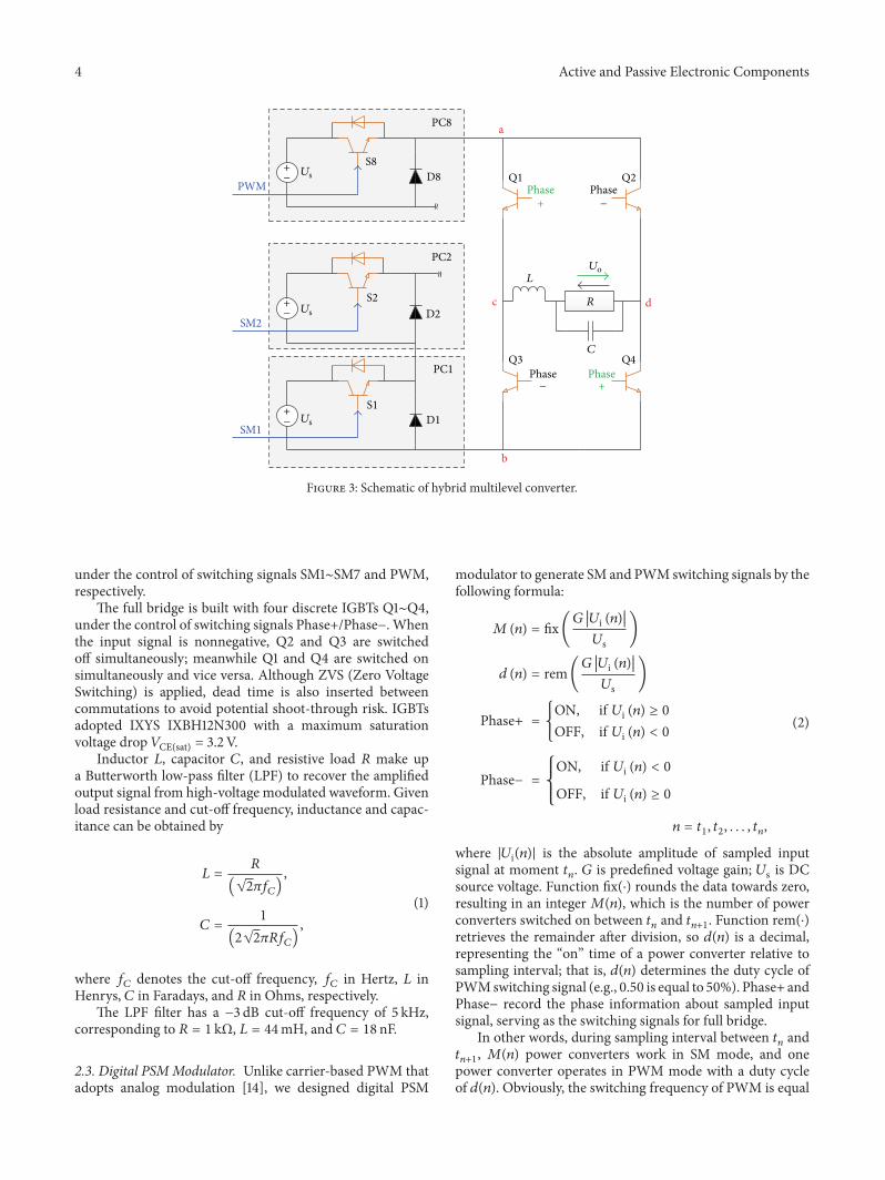
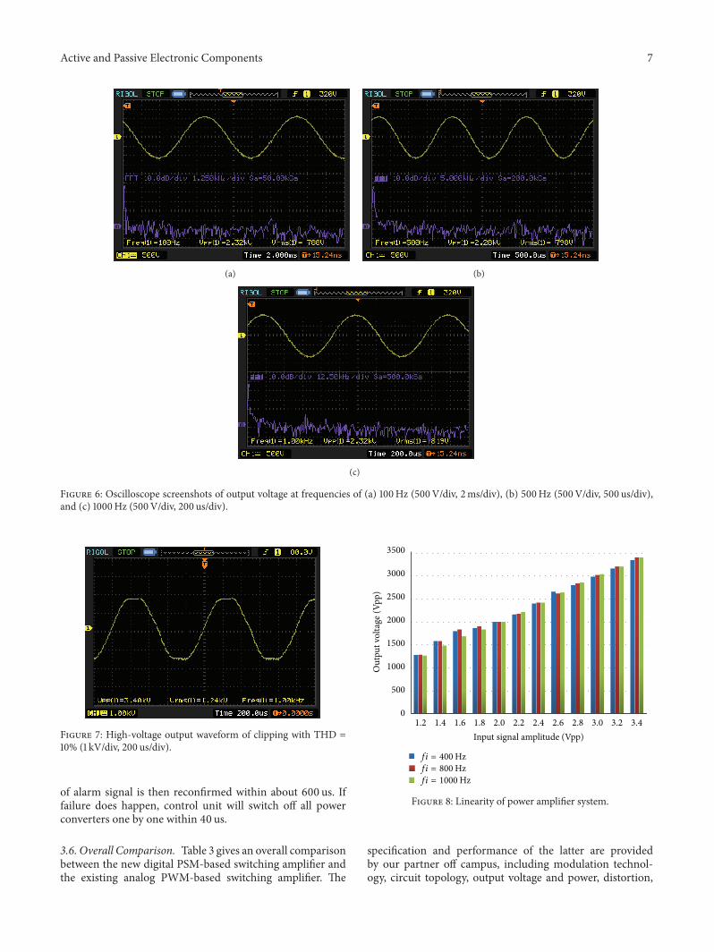
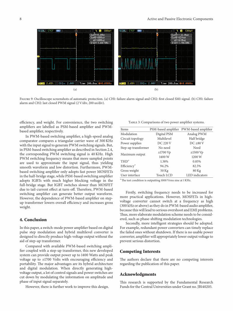

International Journal of
AerospaceEngineeringHindawi Publishing Corporationhttpwwwhindawicom Volume 2014
RoboticsJournal of
Hindawi Publishing Corporationhttpwwwhindawicom Volume 2014
Hindawi Publishing Corporationhttpwwwhindawicom Volume 2014
Active and Passive Electronic Components
Control Scienceand Engineering
Journal of
Hindawi Publishing Corporationhttpwwwhindawicom Volume 2014
International Journal of
RotatingMachinery
Hindawi Publishing Corporationhttpwwwhindawicom Volume 2014
Hindawi Publishing Corporation httpwwwhindawicom
Journal ofEngineeringVolume 2014
Submit your manuscripts athttpwwwhindawicom
VLSI Design
Hindawi Publishing Corporationhttpwwwhindawicom Volume 2014
Hindawi Publishing Corporationhttpwwwhindawicom Volume 2014
Shock and Vibration
Hindawi Publishing Corporationhttpwwwhindawicom Volume 2014
Civil EngineeringAdvances in
Acoustics and VibrationAdvances in
Hindawi Publishing Corporationhttpwwwhindawicom Volume 2014
Hindawi Publishing Corporationhttpwwwhindawicom Volume 2014
Electrical and Computer Engineering
Journal of
Advances inOptoElectronics
Hindawi Publishing Corporation httpwwwhindawicom
Volume 2014
The Scientific World JournalHindawi Publishing Corporation httpwwwhindawicom Volume 2014
SensorsJournal of
Hindawi Publishing Corporationhttpwwwhindawicom Volume 2014
Modelling amp Simulation in EngineeringHindawi Publishing Corporation httpwwwhindawicom Volume 2014
Hindawi Publishing Corporationhttpwwwhindawicom Volume 2014
Chemical EngineeringInternational Journal of Antennas and
Propagation
International Journal of
Hindawi Publishing Corporationhttpwwwhindawicom Volume 2014
Hindawi Publishing Corporationhttpwwwhindawicom Volume 2014
Navigation and Observation
International Journal of
Hindawi Publishing Corporationhttpwwwhindawicom Volume 2014
DistributedSensor Networks
International Journal of