Design of High Speed Hybrid Carry Select Adder - … Carry Select Adder is a particular way to...
6
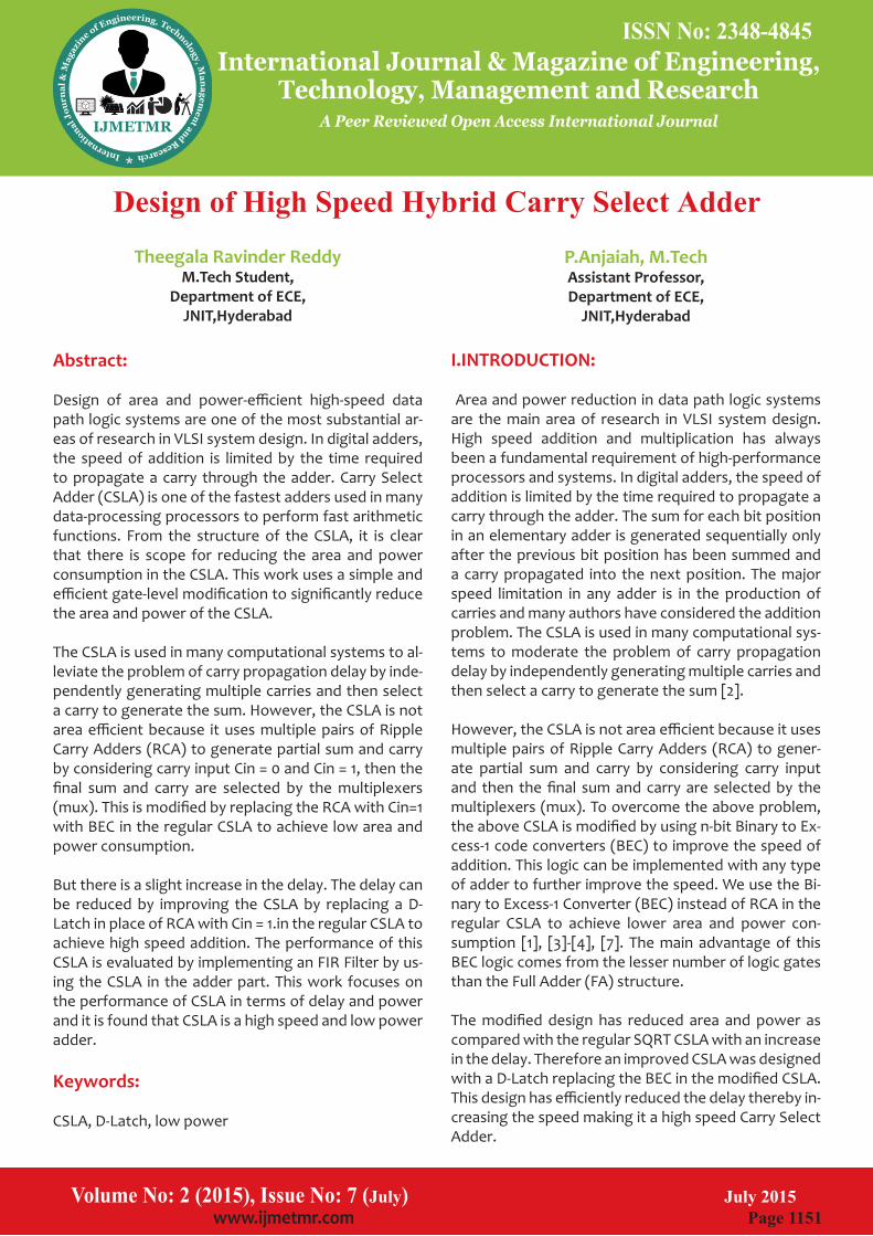
ISSN No: 2348-4845 Volume No: 2 (2015), Issue No: 7 (July) July 2015 www.ijmetmr.com Page 1151 International Journal & Magazine of Engineering, Technology, Management and Research A Peer Reviewed Open Access International Journal I.INTRODUCTION: Area and power reduction in data path logic systems are the main area of research in VLSI system design. High speed addition and multiplication has always been a fundamental requirement of high-performance processors and systems. In digital adders, the speed of addition is limited by the time required to propagate a carry through the adder. The sum for each bit position in an elementary adder is generated sequentially only after the previous bit position has been summed and a carry propagated into the next position. The major speed limitation in any adder is in the production of carries and many authors have considered the addition problem. The CSLA is used in many computational sys- tems to moderate the problem of carry propagation delay by independently generating multiple carries and then select a carry to generate the sum [2]. However, the CSLA is not area efficient because it uses multiple pairs of Ripple Carry Adders (RCA) to gener- ate partial sum and carry by considering carry input and then the final sum and carry are selected by the multiplexers (mux). To overcome the above problem, the above CSLA is modified by using n-bit Binary to Ex- cess-1 code converters (BEC) to improve the speed of addition. This logic can be implemented with any type of adder to further improve the speed. We use the Bi- nary to Excess-1 Converter (BEC) instead of RCA in the regular CSLA to achieve lower area and power con- sumption [1], [3]-[4], [7]. The main advantage of this BEC logic comes from the lesser number of logic gates than the Full Adder (FA) structure. The modified design has reduced area and power as compared with the regular SQRT CSLA with an increase in the delay. Therefore an improved CSLA was designed with a D-Latch replacing the BEC in the modified CSLA. This design has efficiently reduced the delay thereby in- creasing the speed making it a high speed Carry Select Adder. Abstract: Design of area and power-efficient high-speed data path logic systems are one of the most substantial ar- eas of research in VLSI system design. In digital adders, the speed of addition is limited by the time required to propagate a carry through the adder. Carry Select Adder (CSLA) is one of the fastest adders used in many data-processing processors to perform fast arithmetic functions. From the structure of the CSLA, it is clear that there is scope for reducing the area and power consumption in the CSLA. This work uses a simple and efficient gate-level modification to significantly reduce the area and power of the CSLA. The CSLA is used in many computational systems to al- leviate the problem of carry propagation delay by inde- pendently generating multiple carries and then select a carry to generate the sum. However, the CSLA is not area efficient because it uses multiple pairs of Ripple Carry Adders (RCA) to generate partial sum and carry by considering carry input Cin = 0 and Cin = 1, then the final sum and carry are selected by the multiplexers (mux). This is modified by replacing the RCA with Cin=1 with BEC in the regular CSLA to achieve low area and power consumption. But there is a slight increase in the delay. The delay can be reduced by improving the CSLA by replacing a D- Latch in place of RCA with Cin = 1.in the regular CSLA to achieve high speed addition. The performance of this CSLA is evaluated by implementing an FIR Filter by us- ing the CSLA in the adder part. This work focuses on the performance of CSLA in terms of delay and power and it is found that CSLA is a high speed and low power adder. Keywords: CSLA, D-Latch, low power Theegala Ravinder Reddy M.Tech Student, Department of ECE, JNIT,Hyderabad P.Anjaiah, M.Tech Assistant Professor, Department of ECE, JNIT,Hyderabad Design of High Speed Hybrid Carry Select Adder
Transcript of Design of High Speed Hybrid Carry Select Adder - … Carry Select Adder is a particular way to...
ISSN No: 2348-4845
Volume No: 2 (2015), Issue No: 7 (July) July 2015 www.ijmetmr.com Page 1151
International Journal & Magazine of Engineering, Technology, Management and Research
A Peer Reviewed Open Access International Journal
I.INTRODUCTION:
Area and power reduction in data path logic systems are the main area of research in VLSI system design. High speed addition and multiplication has always been a fundamental requirement of high-performance processors and systems. In digital adders, the speed of addition is limited by the time required to propagate a carry through the adder. The sum for each bit position in an elementary adder is generated sequentially only after the previous bit position has been summed and a carry propagated into the next position. The major speed limitation in any adder is in the production of carries and many authors have considered the addition problem. The CSLA is used in many computational sys-tems to moderate the problem of carry propagation delay by independently generating multiple carries and then select a carry to generate the sum [2].
However, the CSLA is not area efficient because it uses multiple pairs of Ripple Carry Adders (RCA) to gener-ate partial sum and carry by considering carry input and then the final sum and carry are selected by the multiplexers (mux). To overcome the above problem, the above CSLA is modified by using n-bit Binary to Ex-cess-1 code converters (BEC) to improve the speed of addition. This logic can be implemented with any type of adder to further improve the speed. We use the Bi-nary to Excess-1 Converter (BEC) instead of RCA in the regular CSLA to achieve lower area and power con-sumption [1], [3]-[4], [7]. The main advantage of this BEC logic comes from the lesser number of logic gates than the Full Adder (FA) structure.
The modified design has reduced area and power as compared with the regular SQRT CSLA with an increase in the delay. Therefore an improved CSLA was designed with a D-Latch replacing the BEC in the modified CSLA. This design has efficiently reduced the delay thereby in-creasing the speed making it a high speed Carry Select Adder.
Abstract:
Design of area and power-efficient high-speed data path logic systems are one of the most substantial ar-eas of research in VLSI system design. In digital adders, the speed of addition is limited by the time required to propagate a carry through the adder. Carry Select Adder (CSLA) is one of the fastest adders used in many data-processing processors to perform fast arithmetic functions. From the structure of the CSLA, it is clear that there is scope for reducing the area and power consumption in the CSLA. This work uses a simple and efficient gate-level modification to significantly reduce the area and power of the CSLA.
The CSLA is used in many computational systems to al-leviate the problem of carry propagation delay by inde-pendently generating multiple carries and then select a carry to generate the sum. However, the CSLA is not area efficient because it uses multiple pairs of Ripple Carry Adders (RCA) to generate partial sum and carry by considering carry input Cin = 0 and Cin = 1, then the final sum and carry are selected by the multiplexers (mux). This is modified by replacing the RCA with Cin=1 with BEC in the regular CSLA to achieve low area and power consumption.
But there is a slight increase in the delay. The delay can be reduced by improving the CSLA by replacing a D-Latch in place of RCA with Cin = 1.in the regular CSLA to achieve high speed addition. The performance of this CSLA is evaluated by implementing an FIR Filter by us-ing the CSLA in the adder part. This work focuses on the performance of CSLA in terms of delay and power and it is found that CSLA is a high speed and low power adder.
Keywords:
CSLA, D-Latch, low power
Theegala Ravinder ReddyM.Tech Student,
Department of ECE,JNIT,Hyderabad
P.Anjaiah, M.Tech Assistant Professor,Department of ECE,
JNIT,Hyderabad
Design of High Speed Hybrid Carry Select Adder
ISSN No: 2348-4845 ISSN No: 2348-4845
Volume No: 2 (2015), Issue No: 7 (July) July 2015 www.ijmetmr.com Page 1152
International Journal & Magazine of Engineering, Technology, Management and Research
A Peer Reviewed Open Access International Journal
A carry-select adder is divided into sectors, each of which, except for the least significant performs two additions in parallel, one assuming a carry-in of zero, the other a carry-in of one within the sector, there are two 4-bit ripple carry adders receiving the same data inputs but different Cin. The upper adder has a carry in of zero, the lower adder a carry-in of one. The actual Cin from the preceding sector selects one of the two adders. If the carry-in is zero, the sum and carry-out of the upper adder are selected. If the carry-in is one, the sum and carry-out of the lower adder are selected. Logically, the result is not different if a single ripple-carry adder were used.
First the coding for full adder and different multiplex-ers of 6:3, 8:4, 10:5, and 12:6 was done. Then 2, 3, 4, 5-bit ripple carry adder was done by calling the full adder. The regular 16- bit CSLA was created by call-ing the ripple carry adders and all multiplexers based on circuit. It has five groups of different size RCA. The delay and area of each group has to be evaluated. To do this, we first need to evaluate the delay and area of each of the basic adder blocks used in the structure of the CSLA. The source code is written for all the above adder blocks like xor gate, half adder, full adder, 2x1 mux, ripple carry adder and carry look ahead adder and finally the Regular carry select adder using VHDL. Simulation will be done to verify the functionality and synthesis will be done to get the NETLIST using Xilinx ISE 13.2i.
III. MODIFIED CARRY SELECT ADDER:
The regular CSLA is not area efficient because it uses multiple pairs of Ripple Carry Adders (RCA) to gener-ate partial sum and carry by considering carry input and then the final sum and carry are selected by the multiplexers (mux). To overcome the above problem, the regular CSLA is modified by using n-bit Binary to Ex-cess-1 code converters (BEC) to improve the speed of addition. This logic can be implemented with any type of adder to further improve the speed.
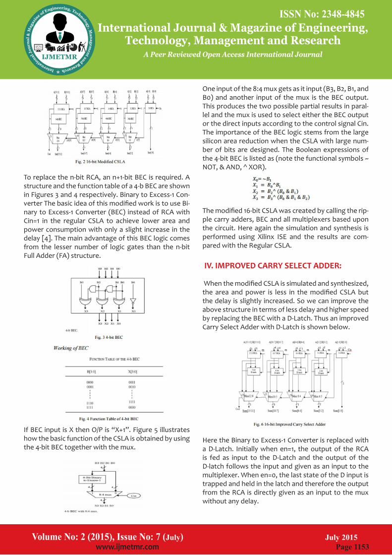
We use the Binary to Excess-1 Converter (BEC) instead of RCA with Cin=1 in the regular CSLA to achieve lower area and power consumption. The below Fig. 2 shows the structure of modified carry select adder.
Digital Signal Processing (DSP) deals with the manipu-lation of digital signals using complex signal process-ing systems built from basic building blocks like filters. The proposed work is implementation in the FIR filter in adder parts. This work evaluates the performance of the improved design in terms of delay and power. This is briefed as follows. First we deal with the delay, area and power evaluation methodology of the basic adder blocks. Next we present the detailed structure and the function of the BEC logic.
The CSLA has been chosen for comparison with the modified and improved design. The delay and power evaluation methodology of the regular, modified and improved SQRT CSLA are presented. Therefore the main aim of the project is to design and implement a high speed carry select adder to enhance the speed of addition and perform fast arithmetic functions. The proposed design is applied to the FIR filter structure in the adder part to evaluate the performance of the pro-posed design. This work estimates the performance of the proposed design in terms of delay and power.
II. 16-BIT REGULAR CARRY SELECT ADDER:
A Carry Select Adder is a particular way to implement an adder, which is a logic element that computes the (n+1) bit sum of two n-bit numbers. The carry-select adder is simple but rather fast. The carry-select adder generally consists of two ripple carry adders and a mul-tiplexer. Adding two n-bit numbers with a carry-select adder is done with two adders (therefore two ripple carry adders) in order to perform the calculation twice, one time with the assumption of the carry being zero and the other assuming one. After the two results are calculated, the correct sum, as well as the correct carry, is then selected with the multiplexer once the correct carry is known. The structure of a 16 bit CSLA is shown below
Volume No: 2 (2015), Issue No: 7 (July) July 2015 www.ijmetmr.com Page 1153
International Journal & Magazine of Engineering, Technology, Management and Research
A Peer Reviewed Open Access International Journal
One input of the 8:4 mux gets as it input (B3, B2, B1, and B0) and another input of the mux is the BEC output. This produces the two possible partial results in paral-lel and the mux is used to select either the BEC output or the direct inputs according to the control signal Cin. The importance of the BEC logic stems from the large silicon area reduction when the CSLA with large num-ber of bits are designed. The Boolean expressions of the 4-bit BEC is listed as (note the functional symbols ~ NOT, & AND, ^ XOR).
The modified 16-bit CSLA was created by calling the rip-ple carry adders, BEC and all multiplexers based upon the circuit. Here again the simulation and synthesis is performed using Xilinx ISE and the results are com-pared with the Regular CSLA.
IV. IMPROVED CARRY SELECT ADDER:
When the modified CSLA is simulated and synthesized, the area and power is less in the modified CSLA but the delay is slightly increased. So we can improve the above structure in terms of less delay and higher speed by replacing the BEC with a D-Latch. Thus an improved Carry Select Adder with D-Latch is shown below.
Here the Binary to Excess-1 Converter is replaced with a D-Latch. Initially when en=1, the output of the RCA is fed as input to the D-Latch and the output of the D-latch follows the input and given as an input to the multiplexer. When en=0, the last state of the D input is trapped and held in the latch and therefore the output from the RCA is directly given as an input to the mux without any delay.
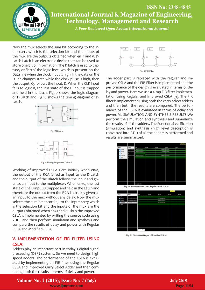
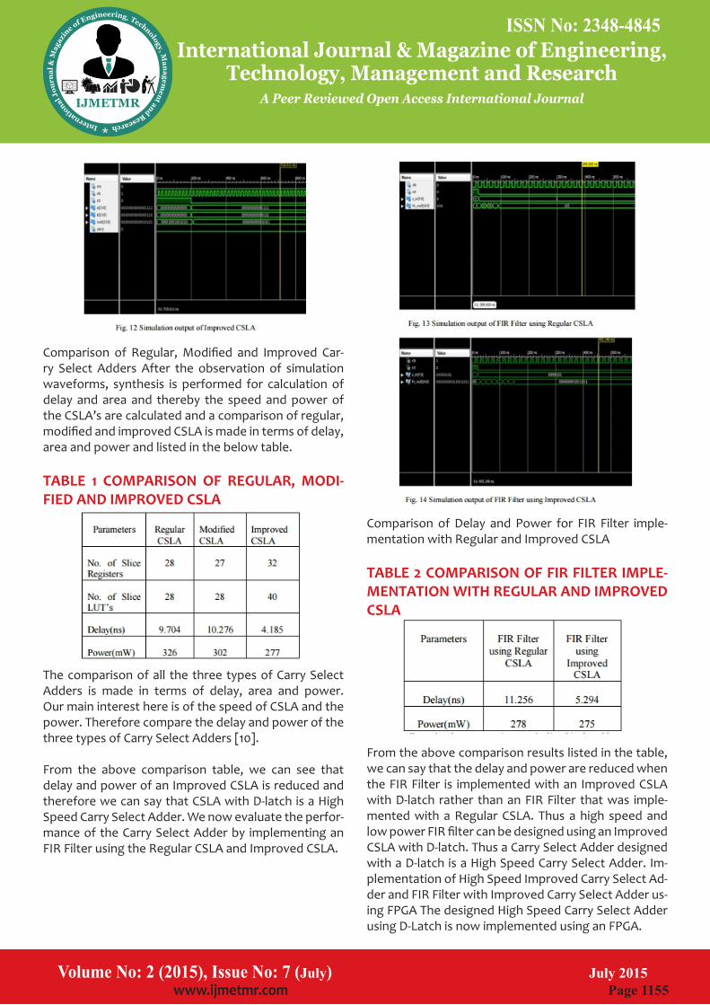
To replace the n-bit RCA, an n+1-bit BEC is required. A structure and the function table of a 4-b BEC are shown in Figures 3 and 4 respectively. Binary to Excess-1 Con-verter The basic idea of this modified work is to use Bi-nary to Excess-1 Converter (BEC) instead of RCA with Cin=1 in the regular CSLA to achieve lower area and power consumption with only a slight increase in the delay [4]. The main advantage of this BEC logic comes from the lesser number of logic gates than the n-bit Full Adder (FA) structure.
If BEC input is X then O/P is “X+1”. Figure 5 illustrates how the basic function of the CSLA is obtained by using the 4-bit BEC together with the mux.
ISSN No: 2348-4845 ISSN No: 2348-4845
Volume No: 2 (2015), Issue No: 7 (July) July 2015 www.ijmetmr.com Page 1152
International Journal & Magazine of Engineering, Technology, Management and Research
A Peer Reviewed Open Access International Journal
A carry-select adder is divided into sectors, each of which, except for the least significant performs two additions in parallel, one assuming a carry-in of zero, the other a carry-in of one within the sector, there are two 4-bit ripple carry adders receiving the same data inputs but different Cin. The upper adder has a carry in of zero, the lower adder a carry-in of one. The actual Cin from the preceding sector selects one of the two adders. If the carry-in is zero, the sum and carry-out of the upper adder are selected. If the carry-in is one, the sum and carry-out of the lower adder are selected. Logically, the result is not different if a single ripple-carry adder were used.
First the coding for full adder and different multiplex-ers of 6:3, 8:4, 10:5, and 12:6 was done. Then 2, 3, 4, 5-bit ripple carry adder was done by calling the full adder. The regular 16- bit CSLA was created by call-ing the ripple carry adders and all multiplexers based on circuit. It has five groups of different size RCA. The delay and area of each group has to be evaluated. To do this, we first need to evaluate the delay and area of each of the basic adder blocks used in the structure of the CSLA. The source code is written for all the above adder blocks like xor gate, half adder, full adder, 2x1 mux, ripple carry adder and carry look ahead adder and finally the Regular carry select adder using VHDL. Simulation will be done to verify the functionality and synthesis will be done to get the NETLIST using Xilinx ISE 13.2i.
III. MODIFIED CARRY SELECT ADDER:
The regular CSLA is not area efficient because it uses multiple pairs of Ripple Carry Adders (RCA) to gener-ate partial sum and carry by considering carry input and then the final sum and carry are selected by the multiplexers (mux). To overcome the above problem, the regular CSLA is modified by using n-bit Binary to Ex-cess-1 code converters (BEC) to improve the speed of addition. This logic can be implemented with any type of adder to further improve the speed.
We use the Binary to Excess-1 Converter (BEC) instead of RCA with Cin=1 in the regular CSLA to achieve lower area and power consumption. The below Fig. 2 shows the structure of modified carry select adder.
Digital Signal Processing (DSP) deals with the manipu-lation of digital signals using complex signal process-ing systems built from basic building blocks like filters. The proposed work is implementation in the FIR filter in adder parts. This work evaluates the performance of the improved design in terms of delay and power. This is briefed as follows. First we deal with the delay, area and power evaluation methodology of the basic adder blocks. Next we present the detailed structure and the function of the BEC logic.
The CSLA has been chosen for comparison with the modified and improved design. The delay and power evaluation methodology of the regular, modified and improved SQRT CSLA are presented. Therefore the main aim of the project is to design and implement a high speed carry select adder to enhance the speed of addition and perform fast arithmetic functions. The proposed design is applied to the FIR filter structure in the adder part to evaluate the performance of the pro-posed design. This work estimates the performance of the proposed design in terms of delay and power.
II. 16-BIT REGULAR CARRY SELECT ADDER:
A Carry Select Adder is a particular way to implement an adder, which is a logic element that computes the (n+1) bit sum of two n-bit numbers. The carry-select adder is simple but rather fast. The carry-select adder generally consists of two ripple carry adders and a mul-tiplexer. Adding two n-bit numbers with a carry-select adder is done with two adders (therefore two ripple carry adders) in order to perform the calculation twice, one time with the assumption of the carry being zero and the other assuming one. After the two results are calculated, the correct sum, as well as the correct carry, is then selected with the multiplexer once the correct carry is known. The structure of a 16 bit CSLA is shown below
Volume No: 2 (2015), Issue No: 7 (July) July 2015 www.ijmetmr.com Page 1153
International Journal & Magazine of Engineering, Technology, Management and Research
A Peer Reviewed Open Access International Journal
One input of the 8:4 mux gets as it input (B3, B2, B1, and B0) and another input of the mux is the BEC output. This produces the two possible partial results in paral-lel and the mux is used to select either the BEC output or the direct inputs according to the control signal Cin. The importance of the BEC logic stems from the large silicon area reduction when the CSLA with large num-ber of bits are designed. The Boolean expressions of the 4-bit BEC is listed as (note the functional symbols ~ NOT, & AND, ^ XOR).
The modified 16-bit CSLA was created by calling the rip-ple carry adders, BEC and all multiplexers based upon the circuit. Here again the simulation and synthesis is performed using Xilinx ISE and the results are com-pared with the Regular CSLA.
IV. IMPROVED CARRY SELECT ADDER:
When the modified CSLA is simulated and synthesized, the area and power is less in the modified CSLA but the delay is slightly increased. So we can improve the above structure in terms of less delay and higher speed by replacing the BEC with a D-Latch. Thus an improved Carry Select Adder with D-Latch is shown below.
Here the Binary to Excess-1 Converter is replaced with a D-Latch. Initially when en=1, the output of the RCA is fed as input to the D-Latch and the output of the D-latch follows the input and given as an input to the multiplexer. When en=0, the last state of the D input is trapped and held in the latch and therefore the output from the RCA is directly given as an input to the mux without any delay.
To replace the n-bit RCA, an n+1-bit BEC is required. A structure and the function table of a 4-b BEC are shown in Figures 3 and 4 respectively. Binary to Excess-1 Con-verter The basic idea of this modified work is to use Bi-nary to Excess-1 Converter (BEC) instead of RCA with Cin=1 in the regular CSLA to achieve lower area and power consumption with only a slight increase in the delay [4]. The main advantage of this BEC logic comes from the lesser number of logic gates than the n-bit Full Adder (FA) structure.
If BEC input is X then O/P is “X+1”. Figure 5 illustrates how the basic function of the CSLA is obtained by using the 4-bit BEC together with the mux.
ISSN No: 2348-4845 ISSN No: 2348-4845
Volume No: 2 (2015), Issue No: 7 (July) July 2015 www.ijmetmr.com Page 1154
International Journal & Magazine of Engineering, Technology, Management and Research
A Peer Reviewed Open Access International Journal
The adder part is replaced with the regular and im-proved CSLA and the FIR Filter is implemented and the performance of the design is evaluated in terms of de-lay and power. Here we use a 4-tap FIR filter implemen-tation using Regular and Improved CSLA [9]. The FIR filter is implemented using both the carry select adders and then both the results are compared. The perfor-mance of the CSLA is evaluated in terms of delay and power. VI. SIMULATION AND SYNTHESIS RESULTS We perform the simulation and synthesis and summarize the results of all the adders. The Functional verification (simulation) and synthesis (high level description is converted into RTL) of all the adders is performed and results are summarized.
Now the mux selects the sum bit according to the in-put carry which is the selection bit and the inputs of the mux are the outputs obtained when en=1 and 0. D-Latch Latch is an electronic device that can be used to store one bit of information. The D latch is used to cap-ture, or ‘latch’ the logic level which is present on the Data line when the clock input is high. If the data on the D line changes state while the clock pulse is high, then the output, Q, follows the input, D. When the CLK input falls to logic 0, the last state of the D input is trapped and held in the latch. Fig. 7 shows the logic diagram of D-Latch and Fig. 8 shows the timing diagram of D-Latch.
Working of Improved CSLA Here initially when en=1, the output of the RCA is fed as input to the D-Latch and the output of the Dlatch follows the input and giv-en as an input to the multiplexer. When en=0, the last state of the D input is trapped and held in the Latch and therefore the output from the RCA is directly given as an input to the mux without any delay. Now the mux selects the sum bit according to the input carry which is the selection bit and the inputs of the mux are the outputs obtained when en=1 and 0. Thus the Improved CSLA is implemented by writing the source code using VHDL and then perform simulation and synthesis and compare the results of delay and power with Regular CSLA and Modified CSLA.
V. IMPLEMENTATION OF FIR FILTER USING CSLA:Adders play an important part in today’s digital signal processing (DSP) systems. So we need to design high speed adders. The performance of the CSLA is evalu-ated by implementing an FIR filter using the Regular CSLA and Improved Carry Select Adder and then com-paring both the results in terms of delay and power.
Volume No: 2 (2015), Issue No: 7 (July) July 2015 www.ijmetmr.com Page 1155
International Journal & Magazine of Engineering, Technology, Management and Research
A Peer Reviewed Open Access International Journal
Comparison of Delay and Power for FIR Filter imple-mentation with Regular and Improved CSLA TABLE 2 COMPARISON OF FIR FILTER IMPLE-MENTATION WITH REGULAR AND IMPROVED CSLA
From the above comparison results listed in the table, we can say that the delay and power are reduced when the FIR Filter is implemented with an Improved CSLA with D-latch rather than an FIR Filter that was imple-mented with a Regular CSLA. Thus a high speed and low power FIR filter can be designed using an Improved CSLA with D-latch. Thus a Carry Select Adder designed with a D-latch is a High Speed Carry Select Adder. Im-plementation of High Speed Improved Carry Select Ad-der and FIR Filter with Improved Carry Select Adder us-ing FPGA The designed High Speed Carry Select Adder using D-Latch is now implemented using an FPGA.
Comparison of Regular, Modified and Improved Car-ry Select Adders After the observation of simulation waveforms, synthesis is performed for calculation of delay and area and thereby the speed and power of the CSLA’s are calculated and a comparison of regular, modified and improved CSLA is made in terms of delay, area and power and listed in the below table.
TABLE 1 COMPARISON OF REGULAR, MODI-FIED AND IMPROVED CSLA
The comparison of all the three types of Carry Select Adders is made in terms of delay, area and power. Our main interest here is of the speed of CSLA and the power. Therefore compare the delay and power of the three types of Carry Select Adders [10].
From the above comparison table, we can see that delay and power of an Improved CSLA is reduced and therefore we can say that CSLA with D-latch is a High Speed Carry Select Adder. We now evaluate the perfor-mance of the Carry Select Adder by implementing an FIR Filter using the Regular CSLA and Improved CSLA.
ISSN No: 2348-4845 ISSN No: 2348-4845
Volume No: 2 (2015), Issue No: 7 (July) July 2015 www.ijmetmr.com Page 1156
International Journal & Magazine of Engineering, Technology, Management and Research
A Peer Reviewed Open Access International Journal
REFERENCES:
[1] B. Ramkumar and Harish M Kittur, “Low Power and Area Efficient Carry Select Adder” IEEE TRANSACTIONS ON VERY LARGE SCALE INTEGRATION (VLSI) SYSTEMS-2011.
[2] Bedrij, O. J., (1962), “Carry-select adder,” IRE Trans. Electron. Comput., pp.340–344 .
[3] Ceiang ,T. Y. and Hsiao,M. J. ,(Oct. 1998 ),“Carry-select adder using single ripple carry adder,” Electron. Lett., vol. 34, no. 22, pp. 2101– 2103
[4] Ramkumar,B. , Kittur, H.M. and Kannan ,P. M. ,(2010 ),“ASIC implementation of modified faster carry save adder,” Eur. J. Sci. Res., vol. 42, no. 1,pp.53–58,2010.
[5] J. M. Rabaey, Digtal Integrated Circuits—A Design Perspective. Upper Saddle River, NJ: Prentice-Hall, 2001.
[6] E. Abu-Shama and M. Bayoumi, “A New cell for low power adders,” in Proc.Int. Midwest Symp. Circuits and Systems, 1995, pp. 1014–1017
[7] Y. Kim and L.-S. Kim, “64-bit carry-select adder with reduced area,”Electron. Lett., vol. 37, no. 10, pp. 614–615, May 2001.
[8] Y. He, C. H. Chang, and J. Gu, “An area efficient 64-bit square root carry-select adder for low power appli-cations,” in Proc. IEEE Int. Symp. Circuits Syst., 2005, vol 4, pp.4082-4085.
[9] Oklobdzija. V. G, “High Speed VLSI Arithmetic Units: Adders and Multipliers”, in “Design of High Per-formance Microprocessor Circuits”, Book edited by A.Chandrakasan, IEEE Press,2000.
[10] Kaushik Roy, Sharat C. Prasad (2000), “Low-Power CMOS VLSI Circuit Design”, John Wiley & Sons, Inc.
The source code is dumped into the FPGA and the re-sults are checked. The steps involved in the implemen-tation of the CSLA using the FPGA are: we first synthe-size the code, generate programming file, create user constraints file (UCF) file by configuring the input and output pins of FPGA, create a cdc file, run the cdc file, make pin connections including clock. Now switch on the Virtex 5 FPGA kit and configure the target device and finally analyze the design using Chipscope Pro Ana-lyzer. This way the high speed CSLA is implemented us-ing the FPGA.
VII. CONCLUSION: All the three models of CSLA are designed and are implemented in vhdl using Xilinx 13.2 ISE tool and the results are compared in terms of delay and power.The CSLA with D-Latch proves to be the High Speed and Low Power CSLA. It is also implemented with virtex 5 FPGA.
The performance of this CSLA in terms of delay and power is evaluated by implementing an FIR Filter by us-ing the CSLA in the adder part and again it proves to be the High Speed and Low Power CSLA.
Thus a high speed and low power FIR filter can be de-signed using an Improved CSLA with D-latch. The Im-proved CSLA architecture is therefore, high speed, low power and efficient for VLSI hardware implementa-tion.
ACKNOWLEDGEMENT: The authors would like to thank Dr. P.Chandra Sekhar, HOD, ECE Department, University College of Engineer-ing, Osmania University for his valuable suggestions for the implementation of this project.
Volume No: 2 (2015), Issue No: 7 (July) July 2015 www.ijmetmr.com Page 1157
International Journal & Magazine of Engineering, Technology, Management and Research
A Peer Reviewed Open Access International Journal