Design of Compact Active EMI Filters to Reduce the CM...
42
2018. 08. 03 Jingook Kim Ulsan National Institute of Science Technology (UNIST) http://icemclab.unist.ac.kr Design of Compact Active EMI Filters to Reduce the CM Conducted Emissions 1 FR-PM-5 - EMI/EMC for Power Electronics Systems
Transcript of Design of Compact Active EMI Filters to Reduce the CM...

2018. 08. 03
Jingook KimUlsan National Institute of Science Technology (UNIST)
http://icemclab.unist.ac.kr
Design of Compact Active EMI Filters to
Reduce the CM Conducted Emissions
1
FR-PM-5 - EMI/EMC for Power Electronics Systems

Outline
• Introduction
• Feed-Forward Voltage-sense Voltage-compensation
(FF-VSVC) AEF
• Voltage-sense Current-compensation (VSCC) AEF
• Other types AEFs
• Conclusion
2

A Passive EMI Filter for both CM and DM
● A typical passive EMI filter consists of a X-cap, CM choke, and Y-cap.● The leakage inductance of CM choke can be used as the DM inductance.● Each filter generates a large impedance mismatching.
X-cap Y-capCM choke
LISN EUT
3[ref] H. W. Ott, Electromagnetic Compatibility Engineering, 2009, Wiley
CM
DM
LISN EUT
LISN EUT
Low Z High Z
High Z Low Z

A good and large CM choke is bulky and costly.
Y-capacitor is limited by the safety regulation on leakage currents.
Limitation in a Passive CM EMI Filter
Attenuation of DM noise by using X-cap is relatively easier.
● For sufficient CM noise reduction, the passive EMI filter with a large CM choke, a large Y-capacitor, or multi-stage filters are necessary.
● Active EMI filters (AEFs) employing active circuit components are also proposed toreduce the low-frequency CM noise in a compact-size and low-cost.
4

Topologies of Active EMI Filter (AEF)
Voltage-sense Current-compensation
Current-sense Voltage-compensation
Voltage-sense Voltage-compensation
Current-sense Current-compensation
Voltage-sense Voltage-compensation Current-sense Current-compensation
[ref] Y. Son, S. Sul, "Generalization of active filters for EMI reduction and harmonics compensation," IEEE Trans. Ind. Appl., vol.42, no.2, pp.545-551, March./April 2006
Feed
-bac
kFe
ed-f
orw
ard
5
6
Current-sense Voltage-compensation
Voltage-sense Voltage-compensation
Voltage-sense Voltage-compensation
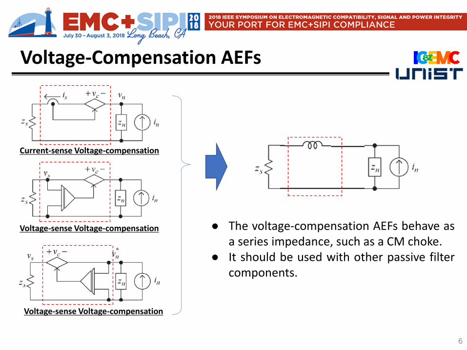
Voltage-Compensation AEFs
● The voltage-compensation AEFs behave asa series impedance, such as a CM choke.
● It should be used with other passive filtercomponents.

7
Voltage-sense Current-compensation
Current-sense Current-compensation
Current-sense Current-compensation
● The voltage-compensation AEFs behave asa shunt impedance, such as a Y-cap.
● It should be used with other filtercomponents.
Current-Compensation AEFs

8
● Immunity against high voltage transient (e.g. surge)– Protection circuits are required, but it should not affect the performance
● Power supply generation for AEF– A DC voltage for AEF can be separately made, but it increases cost and size.– A proper DC voltage is usually available from a gate switching control board.
● Stability in the target applications– Because AEF should be used with other filter components, the stability
condition depends on the condition of filter and EUT.
Critical Issues in applying AEF to AC lines

(AEF Type 1) : FF-VSVC AEF
● Dongil Shin, et al., and Jingook Kim, "Analysis and Design Guide of Active EMI Filter in a Compact Package for Reduction of Common-Mode Conducted Emissions", IEEE Trans on EMC, vol. 57, no. 4, pp. 660-671, Aug. 2015.
9
Voltage-sense Current-compensation
Current-sense Voltage-compensation
Voltage-sense Voltage-compensation
Current-sense Current-compensation
Voltage-sense Voltage-compensation Current-sense Current-compensation
Feed
-bac
kFe
ed-f
orw
ard

Input
Impedance
Impedance
Boosting
Noise
Attenuation
Two Types of VSVC AEF
A-
sLZZ in
1
+=
A-1
1
The attenuation performance ishighest at the unity gain. 1:1 turn ratio transformer unity gain amplifier
Input
Impedance
Impedance
Boosting
Noise
Attenuation
( )( )sLZAZ in ++1=
A+1
1n
n
Z A sL Z
Z sL Z
1
n
n
sL ZZ
A
Z sL Z
The attenuation performance increaseswith the voltage gain (A). High turn ratio transformer required High Gain amplifier required
Feed back type Feed forward type
10
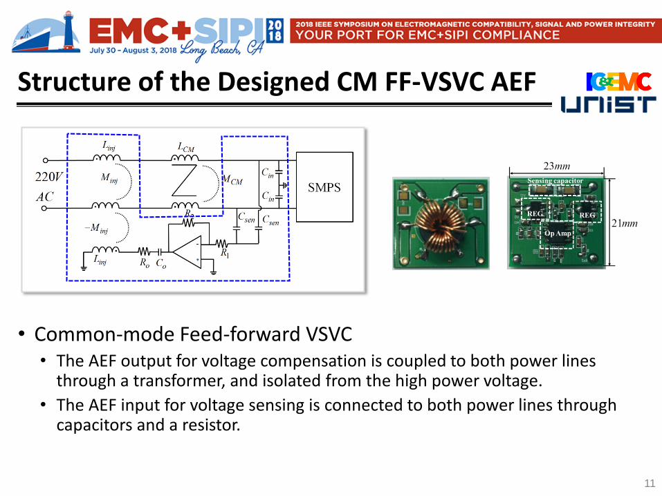
Structure of the Designed CM FF-VSVC AEF
• Common-mode Feed-forward VSVC• The AEF output for voltage compensation is coupled to both power lines
through a transformer, and isolated from the high power voltage.
• The AEF input for voltage sensing is connected to both power lines through capacitors and a resistor.
11

Feedback Loop Gain of the AEF
Stability(Gain margin)
Impedance boosting(Feedback input impedance)v
in
in
in
t
oc A
sCZZ
sCZ
V
VLoopGain
1||
1||
11
1
Disconnect
● Stability and noise attenuation can be analyzed from the feedback loop gain.
Loop Gain
o
oinj
opinj
v
sCRsL
AsMA
1*
LISNinjcmin ZZZZ
1
*
12

Noise Attenuation by Impedance Boosting
• The line impedance of the CM choke ( ) is amplified by .
• The closed-loop gain (Av) should be close to 1 for high impedance boosting.
• The noise attenuation performance of the AEF is achieved by impedance boosting.
LISNinjcmin ZZZZ 1
*
Impedance boostingwhen Av=1
v
in
in
v
in
in
v
in
in
disconininA
Z
sCZ
A
Z
sCZ
A
Z
sCZ
LoopGainZZ
1
||1
||
1
1||
1
1||
1
1 11
11
11
,
Impedance boostingwhen Av=1
1
11
11
AEFw/o,
AEFw/,
||1
||
||1
||1
ZZsC
ZZZZ
ZsC
ZA
Z
i
iNA
n
in
nsCLISNLcm
n
inv
in
CM
CM
in
- Input Impedance
- Noise Attenuation Factor
1inZvA1
1
o
oinj
opinj
v
sCRsL
AsMA
1*
13

Design of FF-VSVC AEF (1) - Cin and Csen
220VAC
injL
CML
CMR
CMC
CML
CMR
CMC
injLoR
injL
oC
2R
1RsenC senC
nZ nI
injM
injM
inC
inC
SMPS
CMM
injM 1Z
1 11
w/o Cin
1
1
|| 2 21 1
22
2
in inn n
v v
Lcm LISN nLcm LISN n
n
Z ZZ Z Z
A ANA
Z Z Z ZZ Z Z
Z Z
≈
1ZZ n
≈
in
LISNLcm
inv
in
n
in
nsCLISNLcm
n
inv
in
sCZZ
sCA
Z
ZZsC
ZZZZ
ZsC
ZA
Z
NA
in
1
1
1
||1
||
||1
||1
1
1
11
11
Cinw/
1
1( || )
n
in
Z ZsC
1
1 1( || )
n
in Y
Z ZsC sC
Ysen
sCsC
11
• A large impedance of CM noise source degrades the noise attenuation.• Cin is required to decrease the effective impedance of CM noise source.• Both Cin and Csen should be smaller than the Y-cap regulation standard.
14
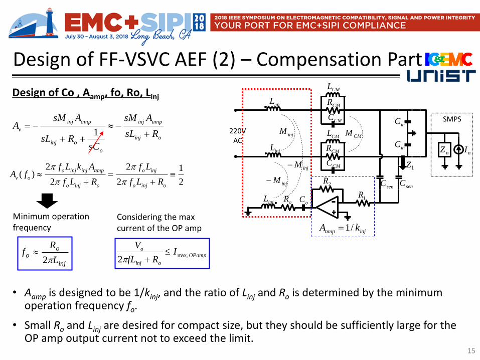
Design of FF-VSVC AEF (2) – Compensation Part
• Aamp is designed to be 1/kinj, and the ratio of Linj and Ro is determined by the minimum operation frequency fo.
• Small Ro and Linj are desired for compact size, but they should be sufficiently large for the OP amp output current not to exceed the limit.
oinj
ampinj
o
oinj
ampinj
vRsL
AsM
sCRsL
AsMA
1
2 2 1( )
2 2 2
o inj inj amp o inj
v o
o inj o o inj o
f L k A f LA f
f L R f L R
inj
oo
L
Rf
2
220VAC
injL
CML
CMR
CMC
CML
CMR
CMC
injLoR
injL
oC
2R
1RsenC senC
nZ nI
injM
injM
inC
inC
SMPS
CMM
injM 1Z
injamp kA /1
Design of Co , Aamp, fo, Ro, Linj
OPamp
oinj
o IRfL
Vmax,
2
Minimum operation frequency
Considering the max current of the OP amp
15
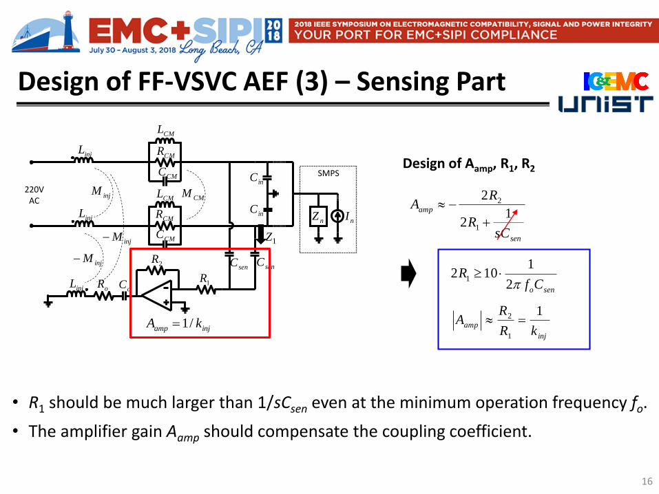
Design of FF-VSVC AEF (3) – Sensing Part
• R1 should be much larger than 1/sCsen even at the minimum operation frequency fo.
• The amplifier gain Aamp should compensate the coupling coefficient.
220VAC
injL
CML
CMR
CMC
CML
CMR
CMC
injLoR
injL
oC
2R
1RsenC senC
nZ nI
injM
injM
inC
inC
SMPS
CMM
injM 1Z
injamp kA /1
sen
amp
sCR
RA
12
2
1
2
1
12 10
2o sen
Rf C
Design of Aamp, R1, R2
inj
ampkR
RA
1
1
2
16

Design of FF-VSVC AEF (4) – Stability Check
• If the feedback system is unstable, the AEF does not work properly or even damaged.
• After the initial design, the stability should be confirmed by checking the gain margin.
• The gain margin increases, as R1 decrease and Ro increases.
2121)(
RC
CC
sen
senp
][2
1
)(
1||2
))((
1||2
12180
180
180180
1
180180
1
dBRMj
sCLjR
CjR
CCjR
ZZZGM
inj
o
injo
p
pin
LISNLinjLcm
2
1
1804
1
)(
11
RCMLMLC seninjinjcmcmin
Fine tune of Ro and R1 according to Gain Margin
17

VNA Measurement vs. Model
01
221
2
VV
VS
02
121
2
/1
VI
VY
18
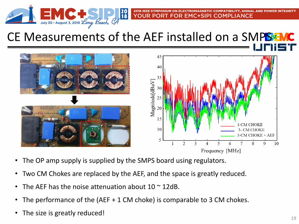
CE Measurements of the AEF installed on a SMPS
• The OP amp supply is supplied by the SMPS board using regulators.
• Two CM Chokes are replaced by the AEF, and the space is greatly reduced.
• The AEF has the noise attenuation about 10 ~ 12dB.
• The performance of the (AEF + 1 CM choke) is comparable to 3 CM chokes.
• The size is greatly reduced!19

Surge Inflow Path to VSVC AEF
The varistors and GDT arrestor cannot block surge under their operating voltage.
Mostly, the varistors and gas discharge tube (GDT) arrestors are installed to primarily suppress the surge voltage and current.
However, they usually operate only for very high surge voltages over several kV.
Surge protection circuits for the AEF should be separately prepared against the surge voltage or current that the varistors and arrestors cannot suppress.
220VAC
injL
CML
CMR
CMC
CML
CMR
CMC
injLoR
injL
oC
2R
1RsenC senC
nZ nI
Varistors
injM
injM
inC
inC
Surge
SMPS
CMMGDT
IsurgeVsurge,sen
injM
Compensation part Sensing part
[Ref] Sangyeong Jeong, Dongil Shin. Jongpil Kim and Seokjoon Kim, and Jingook Kim, “Design of Effective Surge Protection Circuits foran Active EMI filter”, 2017 Asia Pacific EMC conference, Seoul, Korea, June 2017. 20

Overcurrent path to the compensation part
Inducted voltage and current can be generated through the injection transformer.
The current flowing to R2 is almost negligible since R2 is usually much higher than output impedance of Op-amp.
The current injection into the op-amp output stage can be limited by a high value of Ro, but higher Ro degrades the noise attenuation performance at low frequency range.
2R
outopR ,
oRoC
- +injL
1oIoutopI ,
)0(2 RIinjM
injLIsurge
VLinj -
+
2, RR outop 1oosurgeLinj IsLsMIV Limits the inflowing current,but degrades performance of AEF.
21

Surge Protection Circuit for Compensation Part
When the diode is Turn-off :
When the diode is Turn-on :
Linj
popo
po
br VRR
RV
2,1,
2,
br
po
popo
Linj VR
RRV
2,
2,1,
2,2,1,
,
po
br
popo
Linj
outopR
V
RR
VI
,2,1,
2,
Linj
popo
po
br VRR
RV
2R
outopR ,
2, poR1, poR
oC
- +injL
1oIdI
2oIoutopI ,
)0(2 RIinjM
injLIsurge
VLinj -
+
2,1, popoo RRR 2, RR outop
,0dI ,21 oo II
2,
2,
po
Cooutop
R
VII
Vbr : Diode break down voltage
VC : Diode clamping voltage
1
1
o
CLOo
R
VVI
br
po
popo
Linj VR
RRV
2,
2,1,
A transient voltage suppression (TVS) diode is
installed to limit the current and maintain the
design freedom of Ro.
The diode limits the op-amp current as shown in
the right expressions.
The resistor of Ro,p1 should be sufficiently robust
against a large voltage pulse.
22

Overvoltage path to the Sensing part
The sensing part has basically a high input impedance from the AC line, the current is not critical issue but an overvoltage can be induced at the op-amp input, Rop,in.
Most commercial op-amps include internal diodes on each pin for electrostatic discharge (ESD) protection, but the on-chip ESD-diode is not suitable for preventing surges.
External TVS diodes are necessary for reliability from the surges.
senC
inopR , 1RinopV ,
ccV
ccV
Vsurge,sen
inopR ,
ESD-diode inside OP-amp
Break-down voltage of external TVS diodeshould be lower than that of internal ESD diode.
23

Surge Protection Circuit for Sensing Part
The TVS diode can be connected to the node ‘n1’ (option1) and ‘n2’ (option2).
The voltage at the node n2 is larger than the node n1 so the voltage can be more effectively limited in the option 2. However, the junction capacitance of the diode at the ‘option2’ position can degrade the noise attenuation performance of AEF
R1 or R1,p1 should be strong against the overvoltage surge pulse.
senC
inopR ,1,1 pR
2,1 pRinopV ,
ccV
ccV
option1 option2
n2n1
Vsurge,sen
e.g. Anti-surge resistor
21 nn VV
(not recommend this placement since overcurrent can flow to the diode.)
24

2kV Surge Test Set-up
2kV common mode (LINE-GND)surge tests had been performed,and the waveforms are measuredusing an oscilloscope.
The impedance of the CE noisesource is modeled as a capacitorof 40pF, which represents theparasitic capacitance betweenswitching transistors and heatsinks in SMPS.
3.6kV GDT arrestor
Designed AEF
SurgeGen.AC
2.2uFX-cap
420V Varistor
-
+
Currentprobe
AEF PCB
(DUT)
Load model(40pF)
SurgeGenerator
Oscilloscope VoltageSupply for AEF
SupplyProtection
GND
25

Measured Waveform of Compensation Part
About 200mA limited
br
o
ooLinj V
R
RRV
2
21
2
,
o
broutop
R
VI
2
,
o
Coutop
R
VI
br
o
ooLinj V
R
RRV
2
21
Ro,p1 and Ro,p2 are designed as 100 and 30 , respectively, and the clamping voltage of bidirectional TVS diode is around 6V.
The output current of op-amp is limited to about 200mA when large VLinj is induced as shown in the above figures.
When VLinj is small and diode is turn-off, current level is similar. (last peak of current)
2R
2, poR1, poR
oC- +
injL
injM
injL Isurge
VLinj-
+
2,1, popoo RRR
Iop,out
LinjVoutopI ,
Peak values of VLinj are similar
Id
2kV Surge
26

Measured Waveform of Sensing Part
The op-amp input voltage and current arecompared according to the diode position.
The internal ESD-diode are turned on ataround 6V, while the external TVS diode withthe break-down voltage of 3.5V wasimplemented
R1,p1 and R1,p2 are 3.6k and 2k, respectively.
senC
inopR ,1,1 pR
2,1 pR
ccV
ccV
option1 option2
n3n2n1Iop,in
Vop,in
+
-
The internal ESD-diode turn onand inrush current increases
inopI ,
Time (msec)
-0.3
-0.2
-0.1
0
0.05
0 10 20 30 40 50
No Protect.
Input Protect.(opt.1)
Input Protect.(opt.2)
inopV ,
0 0.5 1 1.5 2 2.5-15
-10
-5
0
5
10
15
Time (msec)V
olt
age
(V)
-0.5
Time (msec)0 10 20 30 40 50
-15
-10
-5
0
5
10
15
Vo
ltag
e (V
)
No Protect.
Input Protect.(opt.1)
Input Protect.(opt.2)
inopV ,
2kV Surge
27

Performance Degradation Effect of Diode
02
121
2
/1
VI
VY
104
105
104 105 106 107
Imp
edan
ce (
Oh
m)
w/o AEFw/AEF, no protect.w/AEF, Output protect.w/AEF, Output + input (opt.1) protect.w/AEF, Output + input (opt.2) protect.
Frequency (Hz)
101
102
103
104
105
10621/1 Y
• The 1/Y21 parameter measured by the vector network analyzer (VNA), which can demonstrate the boosting of the power line impedance by the AEF.
• Junction capacitance of 2.5pF can cause performance degradation at high frequency since the additional pole is added in the transfer function.
Results
Output + input (opt.2)protect.
Other cases.
Input protect.option1
Input protect.option2
Output protect.
Port1Port2
VNA Measurement Set-up
28

(AEF Type 2) : VSCC AEF
Voltage-sense Current-compensation
Current-sense Voltage-compensation
Voltage-sense Voltage-compensation
Current-sense Current-compensation
Feed
-bac
k
• Dongil Shin, Sangyeong Jeong, and Jingook Kim, "Quantified Design Guidelines of Compact Transformer -less Active EMI Filter for Performance, Stability, and High Voltage Immunity", IEEE Trans on Power Electronics, vol. 33, no. 8, pp. 6723-6737, Aug. 2018.
29
Voltage-sense Voltage-compensation Current-sense Current-compensation Feed
-fo
rwar
d
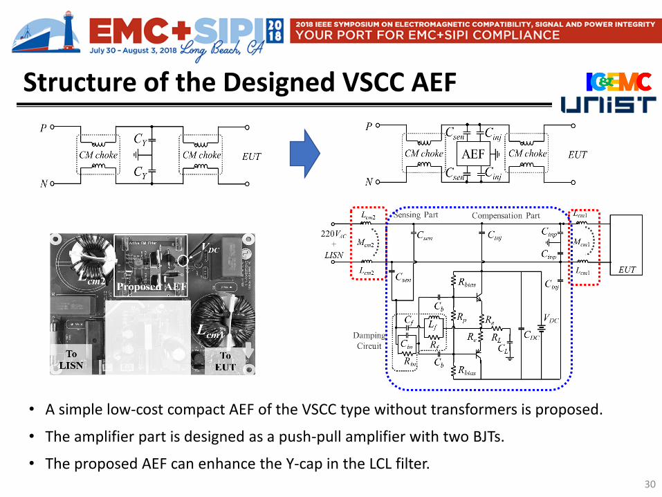
Structure of the Designed VSCC AEF
• A simple low-cost compact AEF of the VSCC type without transformers is proposed.
• The amplifier part is designed as a push-pull amplifier with two BJTs.
• The proposed AEF can enhance the Y-cap in the LCL filter. 30

Loop Gain and Impedance Analysis
,1
AEFin AEF
n t
V AZ
I A
||
A
A
LISNcminpAEF ZZZZ 2||||
LISNcminp
FBsen
f
BJT
mtZZZ
Z
Z
Z
Zg
ZZA
||1||
,
LISNcmn
FBsen
ZZZ
Z
||
,
3211
A
A
III
VZ
fob
AEF
AEF
Zg
ZZ
Z
ZZ
Z
m
BJT
BJTf
FBsen
||||
1
,
(Closed-loop transfer function) =
(Loop gain) =
(AEF impedance) =
31

Noise Attenuation by the AEF
• The effective Y-cap impedance, is much decreased compared to (Zsen||Zinj), which results in a large increase of the NA.
• However, ZAEF below 1kHz is rarely affected by the AEF, and the influence of the AEF on the safety requirements for the leakage current is very small.
inpAEF
inpAEFLISNcm
AEFwLISN
oAEFwLISN
AEFZZ
ZZZZ
I
INA
||
||2
/,
/,
inpinjsen
inpinjsenLISNcm
capYwLISN
capoYwLISN
CapYZZZ
ZZZZZ
I
INA
||||
||||2
/,
/,
32

Design Target of VSCC AEF
0 0
1 22sen
AEF e L
m m L
ZZ R R
Z g g sC
)(
1||,0
injsen
injsenlowAEFCCs
ZZZ
L
L
e
mbias
injsen
highAEF RsC
RgZ
ZZZ 2
21,0
ZAEF without the damping circuitsat the low frequency
at the high frequency
ZAEF0
biasinjsen
injsen
opRCC
CCf
2
• The values of ZAEF0,high and fop should be reduced as much as possible while maintaining the sum of Cinp, Csen, and Cinj to be under the safety limit.
• Cinp are used to screen out the noise source impedance, ZEUT .
No damping circuits
gm : current gain of the BJT
33

Design of Class AB Push-Pull Amplifier
• Re of 1~4 is necessary to stabilize the BJT bias and the thermal runaway of a BJT.• RL should be as small as possible while satisfying the BJT current limit. • Rbias can be determined from the target fop.• DC bias point of the BJT in the class AB amplifier is located slightly above the cutoff, and Rp can be
extracted by solving the KVL from the base to the emitter.
BJT emitter voltage at the sat. region
The amplifier maximum output current
the max limit of the BJT collector current
biasinjsen
injsen
opRCC
CCf
2
CM noise current In
nI,
2
2
DCce sat
e L
VV
R R
,maxc
I
eBCBE
p
biasB
DC
p
bias
p
RIIVR
RIV
RR
R
2
||2
2
2
DC bias analysis of the BJT
34

Damping Circuit Design for System Stability (1)
• In Case 1, after Cf and Rin are added, the filter becomes stable, but its NA performance is poor. • In Case 2, Lf and Cin are inserted at each damping branch to recover the filter performance, but the
resonance between Lf and Cf causes a risk of feedback instability.• In Case 3, Rf is also added to suppress the Q-factor of the resonance. Finally, both stability and
performance of the AEF are optimized.
• The resonance between the CM choke2 and AEF most likely causes the system instability.
• The damping circuits are essential for feedback stability of this AEF.
Resonance
35

Damping Circuit Design for System Stability (2)
• For the system to be stable, the phase of the loop gain, Abt, should remain below 180˚.• The damping circuits should make the filter stable, while maintaining the performance.
Unstable by the resonance
Cf
rf
LLL
f2
1||
4
1
fpres
fLf
C2
,
220
1
fsresffpres LfRLf ,, 2010
fpres
inCf
R,2
1
inpres
in
LL RfC
fCrf ,10
1
21||2
1
Design equations for Damping circuits
36
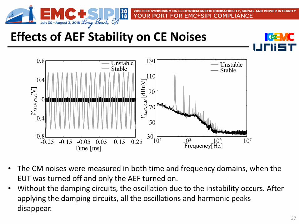
Effects of AEF Stability on CE Noises
• The CM noises were measured in both time and frequency domains, when the EUT was turned off and only the AEF turned on.
• Without the damping circuits, the oscillation due to the instability occurs. After applying the damping circuits, all the oscillations and harmonic peaks disappear.
37
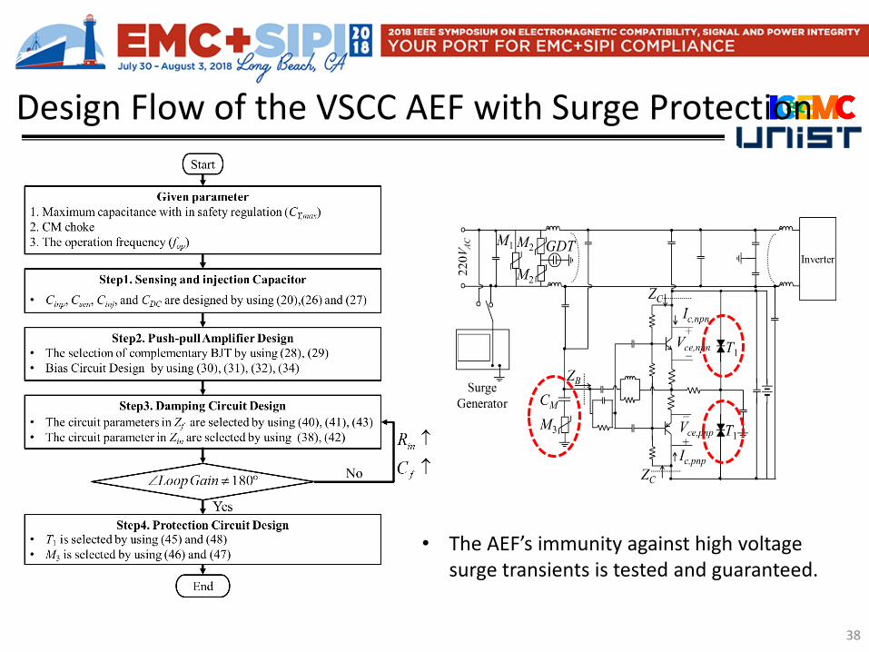
Design Flow of the VSCC AEF with Surge Protection
38
• The AEF’s immunity against high voltage surge transients is tested and guaranteed.

CE Measurements of the AEF installed on an Inverter
• For a fair comparison, the value of CY is set as the sum of Csen, Cinj, and Cinp, which are utilized in the filter with the AEF.
• The AEF is implemented into a real 2.2 kW current resonant inverter, and the CE are reduced by 5dB to 25 dB at a frequency range from 150 kHz to 6 MHz.
• The AEF can be embedded inside a real product without increasing the size and cost.
39

Other developed AEFs
40
• Sangyeong Jeong, et al, Jingook Kim, "A Transformer-Isolated Common-Mode Active EMI Filter without Additional Components on Power Lines", Early Access Articles, IEEE Transactions on Power Electronics, 2018.
• Dongil Shin, et al, Jingook Kim, “A Balanced Feedforward Current-Sense Current-Compensation Active EMI Filter for Common-Mode Noise Reduction”, under revision, IEEE Transactions on EMC, 2018.

41
• E-mail : [email protected]• Webpage : http://emcoretech.com
makes compact Active EMI Filter.
Most of the critical issues havebeen resolved now.(Reliability, immunity, power, stability)

Conclusion
• An EMI filter employing the AEF can be smaller, cheaper, and lighter than a passive-only filter.
• The design guidelines for two types of compact AEFs were derived for performance, stability, and high voltage immunity.
• More reliable other new AEFs are also being developed.• The AEFs are ready to be practically utilized in real home
appliance products.
42