Design of Cmos Receiver by Using Duel Power Linesijrpublisher.com/gallery/54-july-2018.pdf ·...
11
Design of Cmos Receiver by Using Duel Power Lines SHAIK ASMA 1 , K.CHANDRA SEKHAR 2 1 M.Tech (VLSID) in Sri Sai Institute of Technology and Science, Rayachoty, AP. 2 Associate professor in Sri Sai Institute of Technology and Science, Rayachoty, AP. ABSTRACT: The PLC is one in which the power pins and the power distribution networks of ICs are used for data communication as well as power delivery. PLC is used in order to reduce the number of input pins that an IC needs to couple the test data signals to each and every node. Hence to extract the test data signals from this power lines, so many receivers are in need at each and every nodes of the ICs or at places where we have to apply the test. For this purpose, PLC receivers are already designed. But all of them consume very high power. So, in this paper a power efficient CMOS PLC receiver for the same purpose in 180 nm CMOS technology under a supply voltage of 1.8 V is designed with the help of Cadence tool. To achieve this much extreme low power, so many CMOS low power technics are successfully employed like the stacking method, resistor less approach etc. It is found that the power consumption of this new CMOS PLC receiver is only 1.228mW, which is too less than even half power of the presently existing design. Also the receiver is good in keeping the required level of noise immunity and could reduce the area consumption, since the circuit do not have any resistive elements. KEYWORDS: Power Line Communication (PLC), power efficient CMOS PLC receiver, power consumption, stacking method. I. INTRODUCTION Today’s VLSI technology is advancing in such a way that the designers can incorporate a large number of functions inside a chip. Microprocessors are one of the best examples for this. Day by day the size of ICs reduces and the operations it can perform are increasing. So many challenges still exist such as, the need of proper provision for the thermally generated heat removal, the number of the input output pins that an IC needs, proper power supply injection etc., due to which there exists limits on incorporating functions inside ICs. Also routing inside the IC too has a major role in it. There should also be the provisions in ICs like sensors to detect what is happening inside each and every point and if anything happens wrongly, the normal state have to be recovered. Even though the increase in system complexity is an advantage in the sense that the size of ICs can be reduced, with that there should be new inventions for proper data passage inside the same. The power line communication aspect presented in this paper is one of such Methods. In power line communication, it efficiently uses the power distribution networks inside ICs since they are the only components that reach each and every node. So if there have a provision to pass the test data, which are used for fault diagnosis, scan design etc. to whichever areas we need to apply the test that will be an attractive way of communication in ICs, So that the routing overhead inside the ICs to pass these testing data can be intelligently avoided. International Journal of Research Volume 7, Issue VII, JULY/2018 ISSN NO : 2236-6124 Page No:421
Transcript of Design of Cmos Receiver by Using Duel Power Linesijrpublisher.com/gallery/54-july-2018.pdf ·...
Design of Cmos Receiver by Using Duel Power Lines
SHAIK ASMA1, K.CHANDRA SEKHAR2
1 M.Tech (VLSID) in Sri Sai Institute of Technology and Science, Rayachoty, AP.
2 Associate professor in Sri Sai Institute of Technology and Science, Rayachoty, AP.
ABSTRACT:
The PLC is one in which the power pins and
the power distribution networks of ICs are
used for data communication as well as power
delivery. PLC is used in order to reduce the
number of input pins that an IC needs to
couple the test data signals to each and every
node. Hence to extract the test data signals
from this power lines, so many receivers are in
need at each and every nodes of the ICs or at
places where we have to apply the test. For this
purpose, PLC receivers are already designed.
But all of them consume very high power. So,
in this paper a power efficient CMOS PLC
receiver for the same purpose in 180 nm
CMOS technology under a supply voltage of
1.8 V is designed with the help of Cadence
tool. To achieve this much extreme low power,
so many CMOS low power technics are
successfully employed like the stacking
method, resistor less approach etc. It is found
that the power consumption of this new CMOS
PLC receiver is only 1.228mW, which is too
less than even half power of the presently
existing design. Also the receiver is good in
keeping the required level of noise immunity
and could reduce the area consumption, since
the circuit do not have any resistive elements.
KEYWORDS: Power Line Communication
(PLC), power efficient CMOS PLC receiver,
power consumption, stacking method.
I. INTRODUCTION
Today’s VLSI technology is advancing in such
a way that the designers can incorporate a
large number of functions inside a chip.
Microprocessors are one of the best examples
for this. Day by day the size of ICs reduces
and the operations it can perform are
increasing. So many challenges still exist such
as, the need of proper provision for the
thermally generated heat removal, the number
of the input output pins that an IC needs,
proper power supply injection etc., due to
which there exists limits on incorporating
functions inside ICs. Also routing inside the IC
too has a major role in it. There should also be
the provisions in ICs like sensors to detect
what is happening inside each and every point
and if anything happens wrongly, the normal
state have to be recovered. Even though the
increase in system complexity is an advantage
in the sense that the size of ICs can be reduced,
with that there should be new inventions for
proper data passage inside the same. The
power line communication aspect presented in
this paper is one of such Methods. In power
line communication, it efficiently uses the
power distribution networks inside ICs since
they are the only components that reach each
and every node. So if there have a provision to
pass the test data, which are used for fault
diagnosis, scan design etc. to whichever areas
we need to apply the test that will be an
attractive way of communication in ICs, So
that the routing overhead inside the ICs to pass
these testing data can be intelligently avoided.
International Journal of Research
Volume 7, Issue VII, JULY/2018
ISSN NO : 2236-6124
Page No:421
So in PLC, the power distribution networks are
used for power delivery and also data
communication. The test data are
superimposed on the power signal and are
transmitted through the power distribution
networks of ICs rather than the separately
allotted routing paths. Also the number of
power pins can be reduced since there is no
need to carry the test data through the input
pins. Of course, adopting such a power line
communication always has to overcome the
extreme noise level at the power lines. So there
should be effective methods to overcome the
same. Essentially there is the need of receivers
at each and every node to extract these data
signals efficiently from the power lines. Many
variants of the same already exist, but a power
efficient design is not yet met. Why the
receiver should be power efficient is because,
otherwise if each unit of receiver consumes
such huge power, the overall power
consumption of the entire chip will increase by
a large value, which is hard to afford.
In this project, such a power efficient CMOS
PLC receiver is designed in 180nm CMOS
technology under the supply voltage of 1.8 V.
The methods that are incorporated to achieve
the power reduction are very simple to
understand and realize.
II. PREVIOUS WORKS
In PLC area, previous works are already
conducted to reduce the ICs smaller by
incorporating the PLC to reduce the pin
count, area and hence the cost of the chip. So
many such works at the base levels are
already carried out in this area. Works are
conducted in ICs to measure the data
propagation loss from the main power supply
to the internal nodes and also, communication
technologies are put forward such as the Ultra
Wide Band (UWB) and Direct Sequence
Code Division Multiple Access (DS CDMA)
for successful test data passage inside ICs
with reduced noise level.
At first, a data recovery block was designed
which can extract the test data signals from
the power line modulated with impulses in
which Ultra Wide Band communication
technology was adopted. The sensing
scheme inside the recovery block was
designed in such a way that it maintains very
small Power Supply Rejection Ratio(PSRR)
and it is found that the data recovery block
was able to extract the data with about the
amplitude of 90mV and with the period
of300pS. The design was implemented in
TSMC .18µm CMOS technology which had a
power consumption of 2.8mW.
Later, a work on the power distribution
networks of microprocessors is carried out by
using the UWB communication technology
for test data transmission by superimposing
UWB impulses on the power lines. Based on
the resultant characteristics of the PDNs, a
data recovery block design was proposed
and the work was implemented in TSMC
.18µm CMOS technology under a supply
voltage of 1.8 V with a pulse repetition rate of
200MHz and the resultant power consumption
was at about 4.42mW.
A robust receiver for PLC was proposed in
ICs which employs the differential Schmitt
trigger as the third stage of the receiver for
better noise immunity and also to tolerate
supply voltage variations and drops. Thus the
aim was on the robustness and the design
was proposed in .18µm CMOS technology
under a supply voltage of 1.8 V. The
measurement results showed that the receiver
can tolerate up to 22.2% of the supply voltage
International Journal of Research
Volume 7, Issue VII, JULY/2018
ISSN NO : 2236-6124
Page No:422
drop under the signal-to- noise ratio (SNR) of
16.3 dB. The power consumption was
2.4mW.
A PLC receiver was designed in .18µm
CMOS technology under a supply voltage of
1.8 V, which can be applicable to fault
diagnosis, scan design, system debugging like
low data rate communications. The receiver
was designed with three building blocks, the
level shifter, signal extractor, and the logic
restorer. The main aim of this work was not
the high data rate communication, but the
robust operation under variations of supply
voltage and droops. Amplitude Shift Keying
(ASK) approach was put forward for the
superimposition of the test data signals with
the power lines. Adopting binary ASK has
the advantage of less circuit complexity,
simple and easy implementation and hence
lower cost and area. But the main problem
was on the ability to withstand the noise level
that is present in the test data which couples
through the power lines. To overcome the
same, differential concepts are intelligently
employed in the receiver which could achieve
high level of noise rejection. Differential
Schmitt trigger was the key building block in
this design, since it was the major contributor
for the noise immunity. The measurement
results showed that the receiver can tolerate a
voltage drop of up to .423 V, which has a
power dissipation of 3.26mW and a core area
of 74.9 µm × 72.2 µm.
So in this paper, a power efficient CMOS
PLC receiver is designed to extract the test
data signals superimposed on the power lines.
The main aim was the power efficient
operation since power is one of the most
important criterions in the VLSI design. Also
in the PLC, we not only need one or two of
these receivers, but needs it in places
wherever necessary or most probably at each
and every nodes of the ICs. So, if each unit
consumes large power, the total power
consumption of the entire IC will increase
dramatically which is not affordable, and
should mind that these receivers are used only
for extracting the test data signals from the
power lines and there will be so many other
components
Inside the same IC for other operations. So
power efficient design has its own importance
in present VLSI design with increased
complexity especially in microprocessor like
ICs. This paper presents the design of such a
power efficient CMOS PLC receiver in 180
nm CMOS technology under the supply
voltage of 1.8V with the help of Tanner tool.
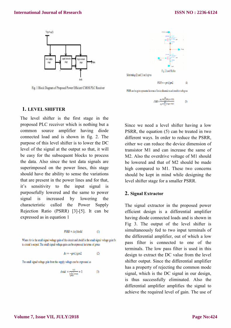
III. PROPOSED POWER EFFICIENT CMOS
PLC RECEIVER
The power efficient CMOS PLC receiver
designed in this paper under a supply voltage
of 1.8 V in 180 nm CMOS technology using
tanner tool consists of three major building
blocks, they are the level shifter, the signal
extractor and the logic restorer. The block
diagram of the proposed receiver is shown in
fig. 1. The test data is represented by Vdd (t)
and the main power signal by VDD. So VDD
+ Vdd (t) represents the test data
superimposed on the power lines. The input
signal is the power line signal in which the
test data is superimposed and it is supplied to
each of the building blocks. The clock signal
of amplitude 0-1.8V is supplied to the logic
restorer. The output of the level shifter is the
input of the signal extractor and the output of
it, which is a differential signal and is applied
to the logic restorer. The detailed operation
and design concepts of each of the building
blocks are described hereafter.
International Journal of Research
Volume 7, Issue VII, JULY/2018
ISSN NO : 2236-6124
Page No:423
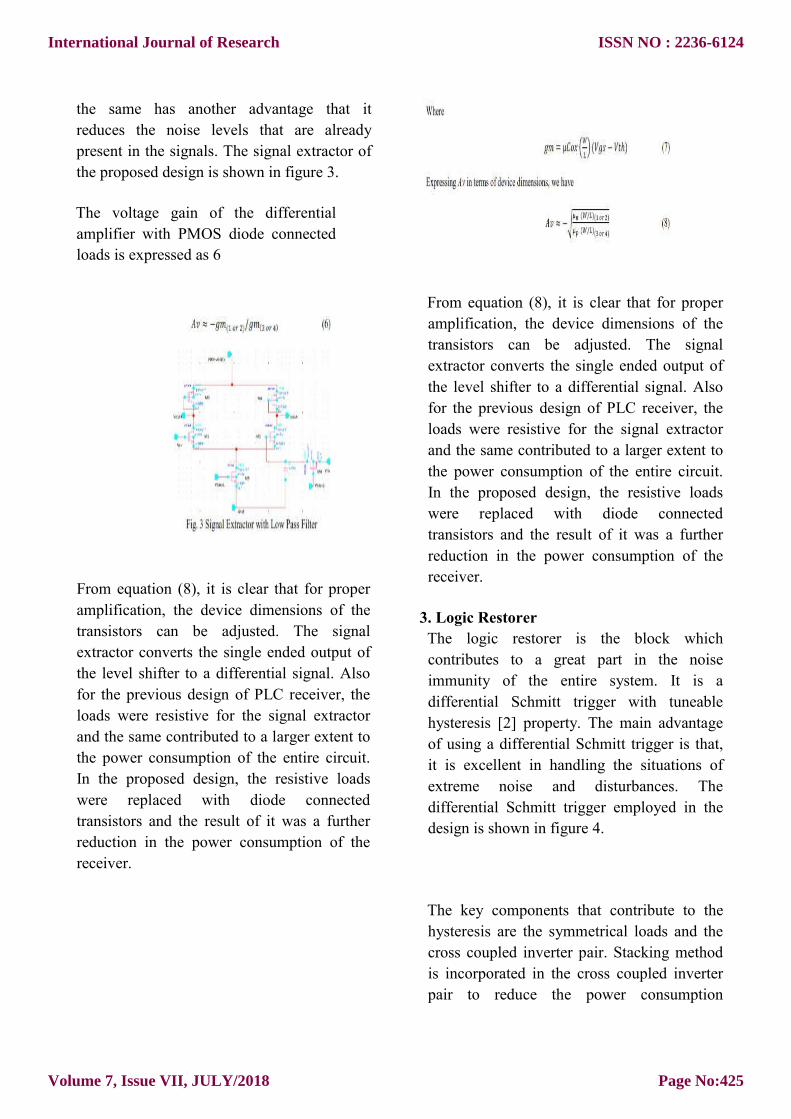
1. LEVEL SHIFTER
The level shifter is the first stage in the
proposed PLC receiver which is nothing but a
common source amplifier having diode
connected load and is shown in fig. 2. The
purpose of this level shifter is to lower the DC
level of the signal at the output so t
be easy for the subsequent blocks to process
the data. Also since the test data signals are
superimposed on the power lines, this stage
should have the ability to sense the variations
that are present in the power lines and for that,
it’s sensitivity to the input signal is
purposefully lowered and the same to power
signal is increased by lowering the
characteristic called the Power Supply
Rejection Ratio (PSRR) [3]-[5]. It can be
expressed as in equation 1
The level shifter is the first stage in the
proposed PLC receiver which is nothing but a
common source amplifier having diode
connected load and is shown in fig. 2. The
purpose of this level shifter is to lower the DC
level of the signal at the output so that, it will
be easy for the subsequent blocks to process
the data. Also since the test data signals are
superimposed on the power lines, this stage
should have the ability to sense the variations
that are present in the power lines and for that,
itivity to the input signal is
purposefully lowered and the same to power
signal is increased by lowering the
characteristic called the Power Supply
[5]. It can be
Since we need a level shifter ha
PSRR, the equation (5) can be treated in two
different ways. In order to reduce the PSRR,
either we can reduce the device dimension of
transistor M1 and can increase the same of
M2. Also the overdrive voltage of M1 should
be lowered and that of
high compared to M1. These two concerns
should be kept in mind while designing the
level shifter stage for a smaller PSRR.
2. Signal Extractor
The signal extractor in the proposed power
efficient design is a differential amplifier
having diode connected loads and is shown in
Fig 3. The output of the level shifter is
simultaneously fed to two input terminals of
the differential amplifier, out of w
pass filter is connected to one of the
terminals. The low pass filter is used in this
design to extract the DC value from the level
shifter output. Since the differential amplifier
has a property of rejecting the common mode
signal, which is the DC signal in our design,
is thus successfully eliminated. Also the
differential amplifier amplifies the signal to
achieve the required level of gain. The use of
Since we need a level shifter having a low
PSRR, the equation (5) can be treated in two
different ways. In order to reduce the PSRR,
either we can reduce the device dimension of
transistor M1 and can increase the same of
M2. Also the overdrive voltage of M1 should
be lowered and that of M2 should be made
high compared to M1. These two concerns
should be kept in mind while designing the
level shifter stage for a smaller PSRR.
The signal extractor in the proposed power
efficient design is a differential amplifier
having diode connected loads and is shown in
Fig 3. The output of the level shifter is
simultaneously fed to two input terminals of
the differential amplifier, out of which a low
pass filter is connected to one of the
terminals. The low pass filter is used in this
design to extract the DC value from the level
shifter output. Since the differential amplifier
has a property of rejecting the common mode
DC signal in our design,
is thus successfully eliminated. Also the
differential amplifier amplifies the signal to
achieve the required level of gain. The use of
International Journal of Research
Volume 7, Issue VII, JULY/2018
ISSN NO : 2236-6124
Page No:424
the same has another advantage that it
reduces the noise levels that are already
present in the signals. The signal extractor of
the proposed design is shown in figure 3.
The voltage gain of the differential
amplifier with PMOS diode connected
loads is expressed as 6
From equation (8), it is clear that for proper
amplification, the device dimensions of the
transistors can be adjusted. The signal
extractor converts the single ended output of
the level shifter to a differential signal. Also
for the previous design of PLC receiver, the
loads were resistive for the signal extractor
and the same contributed to a larger extent to
the power consumption of the entire circuit.
In the proposed design, the resistive loads
were replaced with diode connected
transistors and the result of it was a further
reduction in the power consumption of the
receiver.
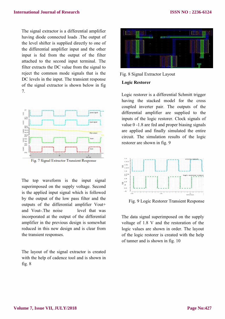
3. Logic Restorer
The logic restorer is the block which
contributes to a great part in the noise
immunity of the entire system. It is a
differential Schmitt trigger with tuneable
hysteresis [2] property. The main advantage
of using a differential Schmitt trigger is that,
it is excellent in handling the situations of
extreme noise and disturbances. The
differential Schmitt trigger employed in the
design is shown in figure 4.
The key components that contribute to the
hysteresis are the symmetrical loads and the
cross coupled inverter pair. Stacking method
is incorporated in the cross coupled inverter
pair to reduce the power consumption
International Journal of Research
Volume 7, Issue VII, JULY/2018
ISSN NO : 2236-6124
Page No:425
considerably. Each transistor in the normal
cross coupled inverter pair is replaced by four
transistors each having a width of W/4 and
due to which the leakage power reduces by a
greater extent. By adjusting the currents
through the symmetrical loads, the
regenerative feedback mechanism of the cross
coupled inverter pair can be adjusted to
control the hysteresis property. Symmetrical
loads are selected to achieve the linearity.
According to the application of the data
signals, the clock signals switches and thus
the currents to the differential amplifie
changes. It simply adjusts the gap between
the low and high threshold voltages and thus
improves the noise immunity of the receiver.
IV. MEASUREMENT RESULTS
The proposed PLC receiver was designed and
simulated in CMOS 0.18-μm technology with
a supply voltage of 1.8 V. The measurement
results followed are of the individual blocks
and after all that of the final PLC receiver.
Also the layouts of individual blocks are
generated. The total power consumption of
the PLC receiver is also calculated.
1. Level Shifter
considerably. Each transistor in the normal
ss coupled inverter pair is replaced by four
transistors each having a width of W/4 and
due to which the leakage power reduces by a
greater extent. By adjusting the currents
through the symmetrical loads, the
regenerative feedback mechanism of the cross
upled inverter pair can be adjusted to
control the hysteresis property. Symmetrical
loads are selected to achieve the linearity.
According to the application of the data
signals, the clock signals switches and thus
the currents to the differential amplifier also
changes. It simply adjusts the gap between
the low and high threshold voltages and thus
improves the noise immunity of the receiver.
The proposed PLC receiver was designed and
m technology with
a supply voltage of 1.8 V. The measurement
results followed are of the individual blocks
and after all that of the final PLC receiver.
Also the layouts of individual blocks are
generated. The total power consumption of
also calculated.
The level shifter that is the common
source amplifier with diode connected
load is simulated with the proper bias
voltage at the gates of the transistor
M2.The timing response obtained is
shown below in fig. 5.
The supply voltage is 1.8 V with the
superposition of the data signal. The top
waveform is the input signal superimposed on
the supply voltage, in which the voltage level
of 1.89 V represents logic 1 and 1.8 V
represents logic0. The bottom waveform
shows the output signal of the level shifter.
The output signal obtained is the level shifted
version of the test data signal which is
superimposed on the power lines.
The layout of the level shifter is created with
the help of cadence tool and is shown in
2. Signal Extractor
The level shifter that is the common
source amplifier with diode connected
load is simulated with the proper bias
voltage at the gates of the transistor
M2.The timing response obtained is
shown below in fig. 5.
supply voltage is 1.8 V with the
superposition of the data signal. The top
waveform is the input signal superimposed on
the supply voltage, in which the voltage level
of 1.89 V represents logic 1 and 1.8 V
represents logic0. The bottom waveform
hows the output signal of the level shifter.
The output signal obtained is the level shifted
version of the test data signal which is
superimposed on the power lines.
The layout of the level shifter is created with
the help of cadence tool and is shown in fig. 6
Signal Extractor
International Journal of Research
Volume 7, Issue VII, JULY/2018
ISSN NO : 2236-6124
Page No:426
The signal extractor is a differential amplifier
having diode connected loads .The output of
the level shifter is supplied directly to one of
the differential amplifier input and the other
input is fed from the output of the filt
attached to the second input terminal. The
filter extracts the DC value from the signal to
reject the common mode signals that is the
DC levels in the input. The transient response
of the signal extractor is shown below in fig
7.
The top waveform is the input signal
superimposed on the supply voltage. Second
is the applied input signal which is followed
by the output of the low pass filter and the
outputs of the differential amplifier Vout+
and Vout-.The noise level that was
incorporated at the output of the differential
amplifier in the previous design is somewhat
reduced in this new design and is clear from
the transient responses.
The layout of the signal extractor is created
with the help of cadence tool and is shown in
fig. 8
The signal extractor is a differential amplifier
having diode connected loads .The output of
the level shifter is supplied directly to one of
the differential amplifier input and the other
input is fed from the output of the filter
attached to the second input terminal. The
filter extracts the DC value from the signal to
reject the common mode signals that is the
DC levels in the input. The transient response
of the signal extractor is shown below in fig
The top waveform is the input signal
superimposed on the supply voltage. Second
is the applied input signal which is followed
by the output of the low pass filter and the
outputs of the differential amplifier Vout+
.The noise level that was
corporated at the output of the differential
amplifier in the previous design is somewhat
reduced in this new design and is clear from
The layout of the signal extractor is created
with the help of cadence tool and is shown in
Fig. 8 Signal Extractor Layout
Logic Restorer
Logic restorer is a differential Schmitt trigger
having the stacked model for the cross
coupled inverter pair. The outputs of the
differential amplifier are supplied to the
inputs of the logic restorer.
value 0 -1.8 are fed and proper biasing signals
are applied and finally simulated the entire
circuit. The simulation results of the logic
restorer are shown in fig. 9
Fig. 9 Logic Restorer Transient Response
The data signal superimposed on the supply
voltage of 1.8 V and the restoration of the
logic values are shown in order. The layout
of the logic restorer is create
of tanner and is shown in fig. 10
Fig. 8 Signal Extractor Layout
Logic restorer is a differential Schmitt trigger
having the stacked model for the cross
coupled inverter pair. The outputs of the
differential amplifier are supplied to the
inputs of the logic restorer. Clock signals of
1.8 are fed and proper biasing signals
are applied and finally simulated the entire
circuit. The simulation results of the logic
restorer are shown in fig. 9
Fig. 9 Logic Restorer Transient Response
superimposed on the supply
voltage of 1.8 V and the restoration of the
logic values are shown in order. The layout
of the logic restorer is created with the help
and is shown in fig. 10
International Journal of Research
Volume 7, Issue VII, JULY/2018
ISSN NO : 2236-6124
Page No:427
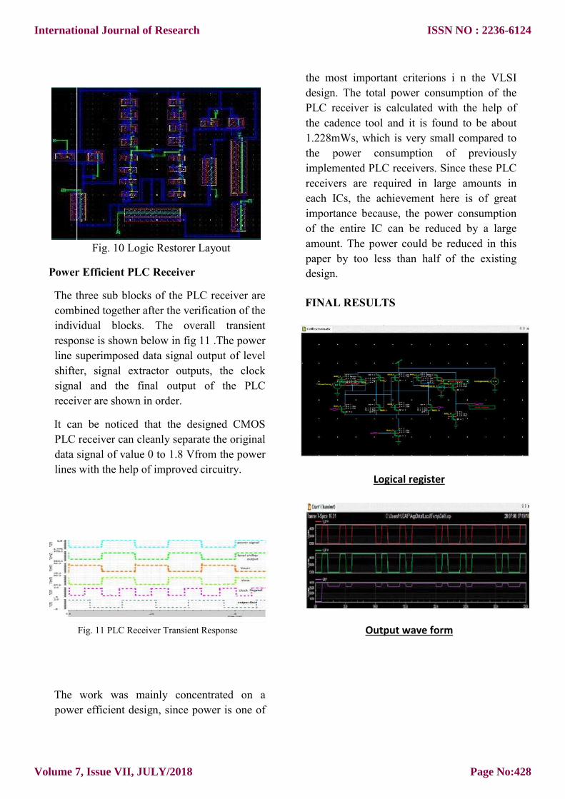
Fig. 10 Logic Restorer Layout
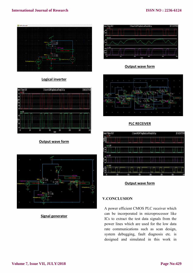
Power Efficient PLC Receiver
The three sub blocks of the PLC receiver are
combined together after the verification of the
individual blocks. The overall transient
response is shown below in fig 11 .The power
line superimposed data signal output of level
shifter, signal extractor outputs, the clock
signal and the final output of the PLC
receiver are shown in order.
It can be noticed that the designed CMOS
PLC receiver can cleanly separate the original
data signal of value 0 to 1.8 Vfrom the power
lines with the help of improved circuitry.
Fig. 11 PLC Receiver Transient Response
The work was mainly concentrated on a
power efficient design, since power is one of
Fig. 10 Logic Restorer Layout
The three sub blocks of the PLC receiver are
combined together after the verification of the
individual blocks. The overall transient
response is shown below in fig 11 .The power
line superimposed data signal output of level
signal extractor outputs, the clock
signal and the final output of the PLC
It can be noticed that the designed CMOS
PLC receiver can cleanly separate the original
data signal of value 0 to 1.8 Vfrom the power
lp of improved circuitry.
Fig. 11 PLC Receiver Transient Response
The work was mainly concentrated on a
power efficient design, since power is one of
the most important criterions i
design. The total power consumption of the
PLC receiver is calculated with the help of
the cadence tool and it is found to be about
1.228mWs, which is very small compared to
the power consumption of previously
implemented PLC receivers. Since t
receivers are required in large amounts in
each ICs, the achievement here is of great
importance because, the power consumption
of the entire IC can be reduced by a large
amount. The power could be reduced in this
paper by too less than half of th
design.
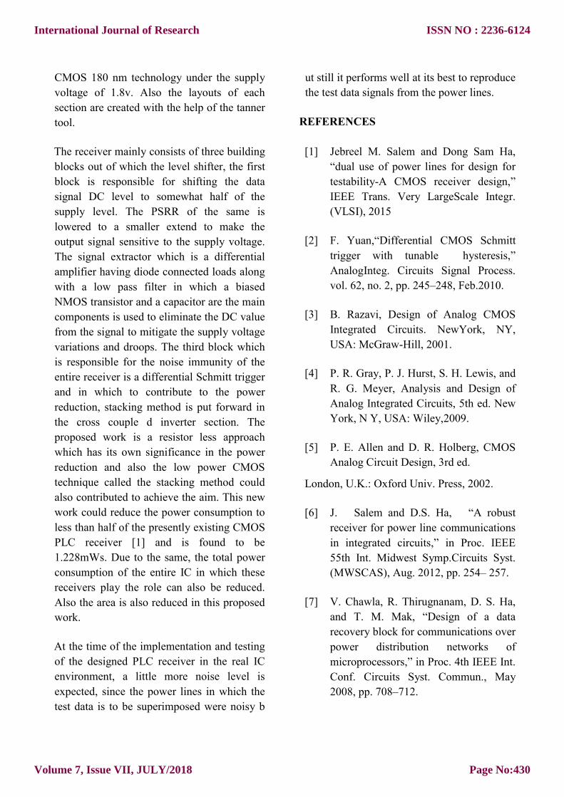
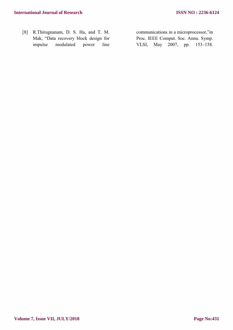
FINAL RESULTS
Logical register
Output wave form
the most important criterions i n the VLSI
design. The total power consumption of the
PLC receiver is calculated with the help of
the cadence tool and it is found to be about
1.228mWs, which is very small compared to
the power consumption of previously
implemented PLC receivers. Since these PLC
receivers are required in large amounts in
each ICs, the achievement here is of great
importance because, the power consumption
of the entire IC can be reduced by a large
amount. The power could be reduced in this
paper by too less than half of the existing
Logical register
Output wave form
International Journal of Research
Volume 7, Issue VII, JULY/2018
ISSN NO : 2236-6124
Page No:428
Logical inverter
Output wave form
Signal generator
Output wave form
PLC RECEIVER
Output wave form
V.CONCLUSION
A power efficient CMOS PLC receiver which
can be incorporated in microprocessor like
ICs to extract the test data signals from the
power lines which are used for the low data
rate communications such as scan design,
system debugging, fault diagnosis etc. is
designed and simulated in this work in
Output wave form
PLC RECEIVER
Output wave form
A power efficient CMOS PLC receiver which
incorporated in microprocessor like
ICs to extract the test data signals from the
power lines which are used for the low data
rate communications such as scan design,
system debugging, fault diagnosis etc. is
designed and simulated in this work in
International Journal of Research
Volume 7, Issue VII, JULY/2018
ISSN NO : 2236-6124
Page No:429
CMOS 180 nm technology under the supply
voltage of 1.8v. Also the layouts of each
section are created with the help of the tanner
tool.
The receiver mainly consists of three building
blocks out of which the level shifter, the first
block is responsible for shifting the data
signal DC level to somewhat half of the
supply level. The PSRR of the same is
lowered to a smaller extend to make the
output signal sensitive to the supply voltage.
The signal extractor which is a differential
amplifier having diode connected loads along
with a low pass filter in which a biased
NMOS transistor and a capacitor are the main
components is used to eliminate the DC value
from the signal to mitigate the supply voltage
variations and droops. The third block which
is responsible for the noise immunity of the
entire receiver is a differential Schmitt trigger
and in which to contribute to the power
reduction, stacking method is put forward in
the cross couple d inverter section. The
proposed work is a resistor less approach
which has its own significance in the power
reduction and also the low power CMOS
technique called the stacking method could
also contributed to achieve the aim. This new
work could reduce the power consumption to
less than half of the presently existing CMOS
PLC receiver [1] and is found to be
1.228mWs. Due to the same, the total power
consumption of the entire IC in which these
receivers play the role can also be reduced.
Also the area is also reduced in this proposed
work.
At the time of the implementation and testing
of the designed PLC receiver in the real IC
environment, a little more noise level is
expected, since the power lines in which the
test data is to be superimposed were noisy b
ut still it performs well at its best to reproduce
the test data signals from the power lines.
REFERENCES
[1] Jebreel M. Salem and Dong Sam Ha,
“dual use of power lines for design for
testability-A CMOS receiver design,”
IEEE Trans. Very LargeScale Integr.
(VLSI), 2015
[2] F. Yuan,“Differential CMOS Schmitt
trigger with tunable hysteresis,”
AnalogInteg. Circuits Signal Process.
vol. 62, no. 2, pp. 245–248, Feb.2010.
[3] B. Razavi, Design of Analog CMOS
Integrated Circuits. NewYork, NY,
USA: McGraw-Hill, 2001.
[4] P. R. Gray, P. J. Hurst, S. H. Lewis, and
R. G. Meyer, Analysis and Design of
Analog Integrated Circuits, 5th ed. New
York, N Y, USA: Wiley,2009.
[5] P. E. Allen and D. R. Holberg, CMOS
Analog Circuit Design, 3rd ed.
London, U.K.: Oxford Univ. Press, 2002.
[6] J. Salem and D.S. Ha, “A robust
receiver for power line communications
in integrated circuits,” in Proc. IEEE
55th Int. Midwest Symp.Circuits Syst.
(MWSCAS), Aug. 2012, pp. 254– 257.
[7] V. Chawla, R. Thirugnanam, D. S. Ha,
and T. M. Mak, “Design of a data
recovery block for communications over
power distribution networks of
microprocessors,” in Proc. 4th IEEE Int.
Conf. Circuits Syst. Commun., May
2008, pp. 708–712.
International Journal of Research
Volume 7, Issue VII, JULY/2018
ISSN NO : 2236-6124
Page No:430
[8] R.Thirugnanam, D. S. Ha, and T. M.
Mak, “Data recovery block design for
impulse modulated power line
communications in a microprocessor,”in
Proc. IEEE Comput. Soc. Annu. Symp.
VLSI, May 2007, pp. 153–158.
International Journal of Research
Volume 7, Issue VII, JULY/2018
ISSN NO : 2236-6124
Page No:431