Design of a Multiple Microcontroller Electronic Control...
84
Design of a Multiple Microcontroller Electronic Control System for Walking Robots A Design Project Report Presented to the Engineering Division of the Graduate School of Cornell University in Partial Fulfillment of the Requirements for the Degree of Masters of Engineering (Electrical) by Hsiang Wei Lee Project Advisor: Bruce R. Land Degree Date: May 2008
Transcript of Design of a Multiple Microcontroller Electronic Control...
Design of a Multiple Microcontroller Electronic Control System
for Walking Robots
A Design Project Report
Presented to the Engineering Division of the Graduate School
of Cornell University
in Partial Fulfillment of the Requirements for the Degree of
Masters of Engineering (Electrical)
by
Hsiang Wei Lee
Project Advisor: Bruce R. Land
Degree Date: May 2008
Abstract
Masters of Electrical Engineering Program
Cornell University
Design Project Report
Project Title:
Design of a Multiple Microcontroller Electronic Control System for Walking Robots
Author:
Hsiang Wei Lee
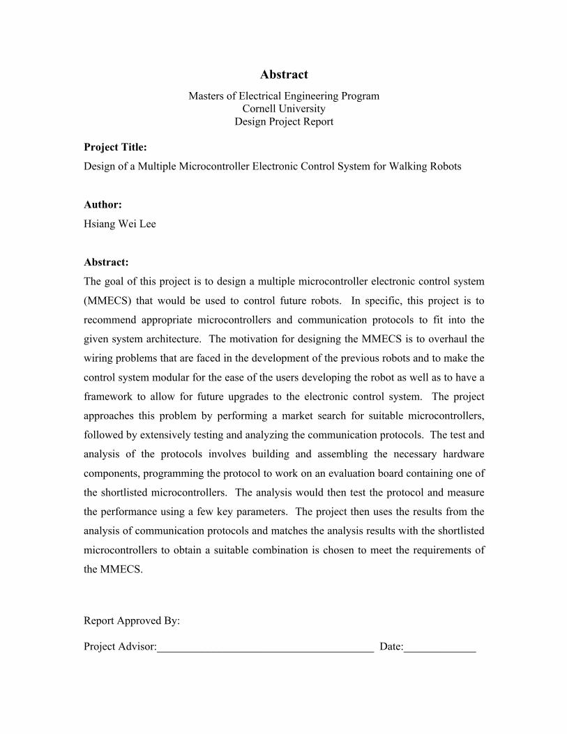
Abstract:
The goal of this project is to design a multiple microcontroller electronic control system
(MMECS) that would be used to control future robots. In specific, this project is to
recommend appropriate microcontrollers and communication protocols to fit into the
given system architecture. The motivation for designing the MMECS is to overhaul the
wiring problems that are faced in the development of the previous robots and to make the
control system modular for the ease of the users developing the robot as well as to have a
framework to allow for future upgrades to the electronic control system. The project
approaches this problem by performing a market search for suitable microcontrollers,
followed by extensively testing and analyzing the communication protocols. The test and
analysis of the protocols involves building and assembling the necessary hardware
components, programming the protocol to work on an evaluation board containing one of
the shortlisted microcontrollers. The analysis would then test the protocol and measure
the performance using a few key parameters. The project then uses the results from the
analysis of communication protocols and matches the analysis results with the shortlisted
microcontrollers to obtain a suitable combination is chosen to meet the requirements of
the MMECS.
Report Approved By:
Project Advisor:_______________________________________ Date:_____________
Executive Summary
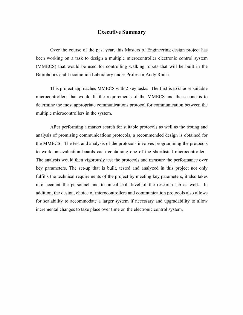
Over the course of the past year, this Masters of Engineering design project has
been working on a task to design a multiple microcontroller electronic control system
(MMECS) that would be used for controlling walking robots that will be built in the
Biorobotics and Locomotion Laboratory under Professor Andy Ruina.
This project approaches MMECS with 2 key tasks. The first is to choose suitable
microcontrollers that would fit the requirements of the MMECS and the second is to
determine the most appropriate communications protocol for communication between the
multiple microcontrollers in the system.
After performing a market search for suitable protocols as well as the testing and
analysis of promising communications protocols, a recommended design is obtained for
the MMECS. The test and analysis of the protocols involves programming the protocols
to work on evaluation boards each containing one of the shortlisted microcontrollers.
The analysis would then vigorously test the protocols and measure the performance over
key parameters. The set-up that is built, tested and analyzed in this project not only
fulfills the technical requirements of the project by meeting key parameters, it also takes
into account the personnel and technical skill level of the research lab as well. In
addition, the design, choice of microcontrollers and communication protocols also allows
for scalability to accommodate a larger system if necessary and upgradability to allow
incremental changes to take place over time on the electronic control system.
- ! -"
Contents
Contents i
List of Figures and Tables iii
1. Introduction 1
1.1. Motivation 1
1.2. Multiple Microcontroller Electronic Control System 3
1.2.1. High Level Portion 4
1.2.2. Communications Level Portion 5
1.2.3. Low Level Portion 5
1.3. Structure of Report 6
2. Design Problem 7
2.1. Problem Formulation 7
2.2. Design Requirements 7
2.3. Design Goal 8
3. Analysis of the Multiple Microcontroller Electronic Control System 8
4. Short-listing Microcontrollers 11
5. Evaluating Protocols 13
5.1. Controller Area Network (CAN-Bus) 14
5.1.1 Overview 14
5.1.2. Potential 16
5.1.3. Experimental Setup and Testing 17
5.1.4. Results 18
- !! -"
5.2. Universal Serial Bus (USB) 20
5.2.1 Overview 20
5.2.2. Potential 22
5.2.3. Experimental Setup and Testing 22
5.2.4. Results 24
5.3. Serial Peripheral Interface with Direct Memory Access 26
5.3.1a. Overview – SPI 26
5.3.1b. Overview – DMA 27
5.3.2. Potential 28
5.3.3. Experimental Setup and Testing 29
5.3.4. Results 30
6. Choosing Microcontrollers and Protocols 33
7. Initial Progress in Building the MMECS 36
7.1. Setting Up Initial Base Code 36
7.1.1. Details of Initial Base Code 36
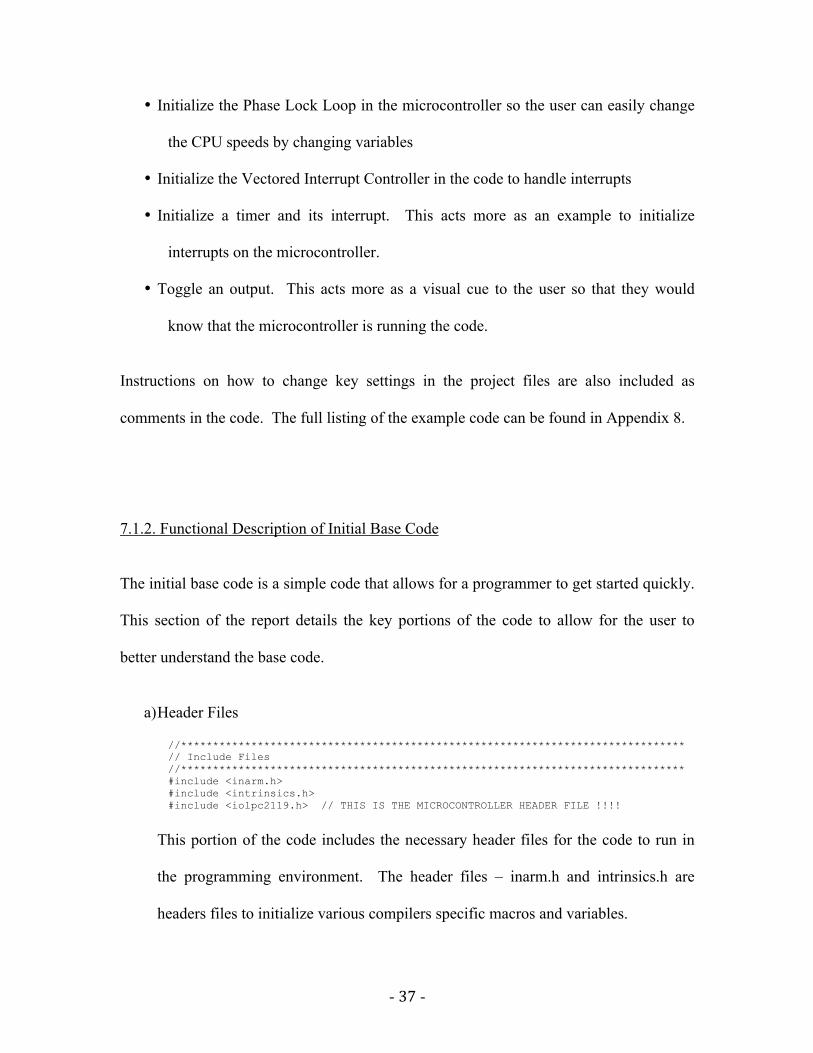
7.1.2. Functional Description of Initial Base Code 37
7.2. Designing the Communications Microcontroller 40
8. Conclusion 41
9. References 42
- !!! -"
List of Figures and Tables
Figure 1: Wiring Problems of MWB
Figure 2: Wiring Problems of Cornell Ranger
Figure 3: Overview of the Proposed Electronic System Architecture
Figure 4: High Level View of a Typical CAN-Bus network
Figure 5: MAC7111 Low Cost Evaluation Board
Figure 6: Concept of Endpoints in USB
Figure 7: Screen Capture of a USB data typical rate test
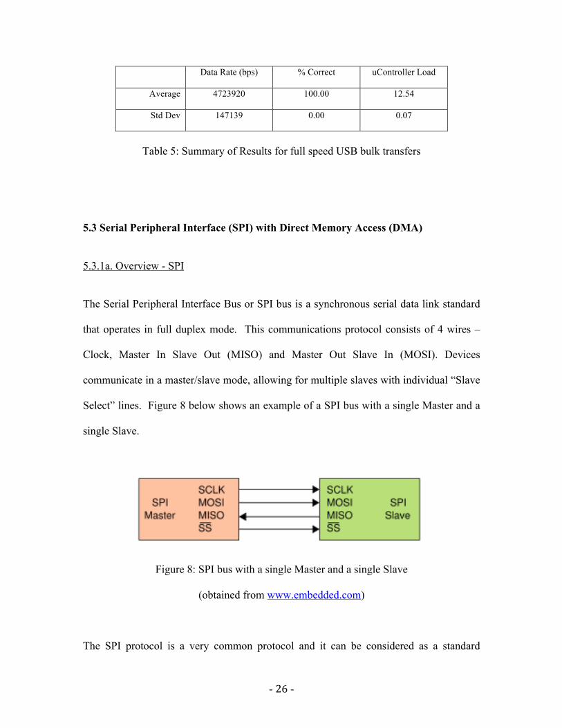
Figure 8: SPI bus with a single Master and a single Slave
Figure 9: Differences in Data Transfers for SPI using DMA and not using DMA
Table 1: Requirements and the bandwidth that is needed.
Table 2: CAN-Bus Maximum Bit Rate vs. Bus Length
Table 3a: CAN Bus Data rates in kbps
Table 3b: CAN Bus Data rates in percentage of the stated CAN Bus speed
Table 4: Parameters used in experiment
Table 5: Summary of Results for full speed USB bulk transfers
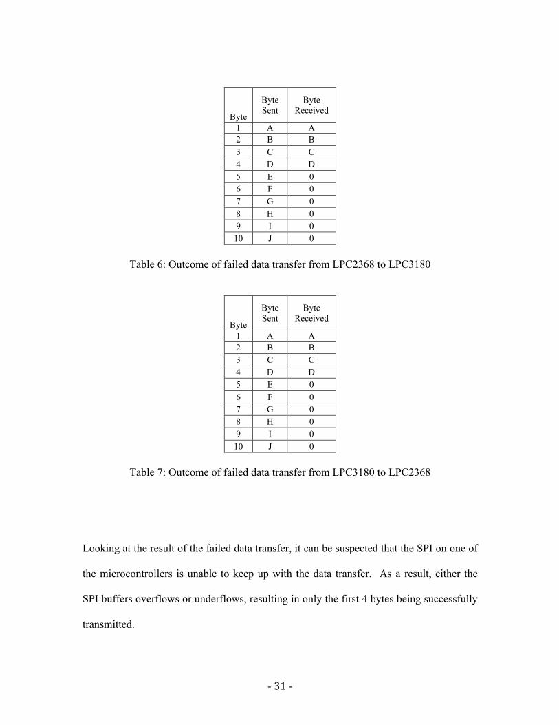
Table 6: Outcome of failed data transfer from LPC2368 to LPC3180
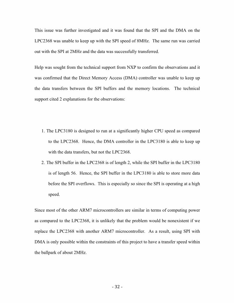
Table 7: Outcome of failed data transfer from LPC3180 to LPC2368
- # -"
1. Introduction
1.1. Motivation
The motivation for designing a new electronic control system is threefold. Firstly, we
hope to be able to implement a modular system of design for the electronic components.
From our previous experiences of designing the Cornell Ranger as well as the Marathon
Walker Bot (MWB), where the electronic components were integrated in a less modular
manner, the programmers often had difficulty finding bugs in the code when a
programming error was suspected. A less modular system also leads to a small group
doing most of the code due to the laborious process of integrating various portions of the
code. With a more modular system design, however, debugging code and testing
programs can be simplified as we are able to test individual components and more people
can participate in programming due to the very fact that it is more modular in nature. The
second motivation of studying this new system is that we hope to find a solution to the
massive wiring issues that plague not only the Cornell Ranger but also the MWB. Figure
1 and Figure 2 shows the wiring problem that has plagued the two robots. Referring to
the two figures below, it can be seen that the wires in the robot are mainly ribbon cables
and these ribbon cables tend to undergo repeated flexes. This set-up results in the wires
in the ribbon cables to break over time and the connection become intermittent and cause
problems for the robot. Another problem is that the wires are placed close to the
actuators. When the ribbon cables and the circuit board are placed into their respective
enclosures, the cables often needs to be “stuffed” into the enclosure and this ocassionally
results in the cables interfering with the moving parts of the actuator.

- $ -"
Figure 1 : Wiring Problems of MWB
Figure 2 : Wiring Problems of Cornell Ranger
The third motivation is to create an electronic control system that has the capacity to
handle the more demanding requirements of future walking robots. Since the process of
designing an electronic control system from the ground up is very time consuming, the
design of the electronic control system has to allow it to be upgradable.
!!
!
!"#$%&!'(!)"%"*#!+%,-.&/0!,1!23&!4)5!
!
!"#$%&!6(!)"%"*#!+%,-.&/0!,1!23&!7,%*&..!89*#&%!
)3&*! 9! %,-,2! "0! "*! "20! :&0"#*! ;390&<! "2! "0! $0$9..=! 23&! >90&! 2392!?&! :,! *,2! 1,%&0&&! 9..! 23&!
>,/;,*&*20!2392!9%&!*&&:&:!2,!/9@&!"2!?9.@A!!B0!0$>3<!?3&*!23&!;%"*2&:!>"%>$"2!-,9%:!C+75D!"0!
:&0"#*&:! 9*:! /9*$19>2$%&:<! "2! "0! %9%&.=! 0&.1! 0$11">"&*2! 9*:! 9::"2",*9.! >,/;,*&*20! 9./,02!
:&1"*"2&.=! 39E&! 2,! -&! 9::&:! ,*2,! 23&! &F"02"*#! >"%>$"2%=A! !)"23! 23&! 9::"2",*! ,1! >,/;,*&*20!
,$20":&!,1!23,0&!9.%&9:=!,*!23&!+75<!"2!"0!*&>&009%=!2,!>,**&>2!E,.29#&!9*:!#%,$*:!."*&0!90!?&..!
90!:929!>9-.&0!1%,/!23&!/">%,>,*2%,..&%!2,!23&!9::&:!,*!>,/;,*&*2A!!G3"0!%&0$.20!"*!*,2!,*.=!9*!
$*0"#32.=! *&02! ,1! ?"%&0<! -$2! 9.0,! 23&! $*>&%29"*2=! ,1! 39E"*#! 9! -9:! >,**&>2",*! ?3&*&E&%!
0,/&23"*#!19".0!2,!?,%@<!"*02&9:!,1!@*,?"*#!2392!"2!H!9!0,12?9%&!;%,-.&/A!
!
- % -"
When a robot is in its design phase, it is usually the case that we do not foresee all the
components that are needed to make it walk. As such, when the printed circuit board
(PCB) is designed and manufactured, it is rarely self sufficient and additional
components almost always have to be added onto the existing circuitry. With the addition
of components outside of those already on the PCB, it is necessary to connect voltage and
ground lines as well as data cables from the microcontroller to the added on component.
This results in not only an unsightly nest of wires, but also the uncertainty of having a
bad connection whenever something fails to work, instead of knowing that it is a software
problem.
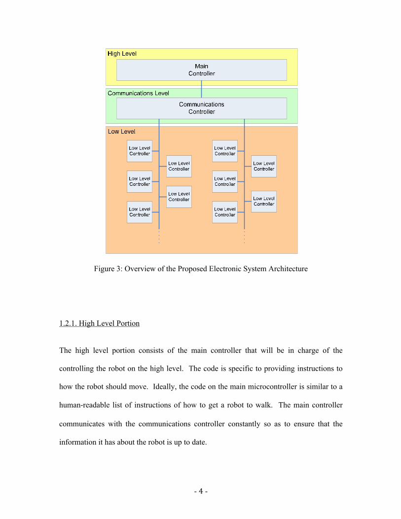
1.2. Multiple Microcontroller Electronic Control System
The multiple microcontroller model that is being studied for the next robot proposes
using multiple microcontrollers communicating with each other to control various parts
of the robot. The model consists of the high level portion, communications level portion
and the low level portion. The 3 main portions, as seen in Figure 3, are the High Level
portion, the Communications Level portion and the Low Level portion.
- & -"
Figure 3: Overview of the Proposed Electronic System Architecture
1.2.1. High Level Portion
The high level portion consists of the main controller that will be in charge of the
controlling the robot on the high level. The code is specific to providing instructions to
how the robot should move. Ideally, the code on the main microcontroller is similar to a
human!readable list of instructions of how to get a robot to walk. The main controller
communicates with the communications controller constantly so as to ensure that the
information it has about the robot is up to date.
!!
!"!#$%&'()"*+,$-!.'-$/!!
!"#! $#%&'()"*+,#-!.'-#/! %"+%! 0,! *#0$1! ,%2-0#-! 3'(! %"#! $#4%! ('*'%! 5('5',#,! 2,0$1!.2/%05/#!
.06('6'$%('//#(,! %'! 6'$%('/! 7+(0'2,!5+(%,!'3! %"#! ('*'%8! ! !"#!.'-#/! 6'$,0,%,!'3! %"#!"01"! /#7#/!
5'(%0'$9!6'..2$06+%0'$,!/#7#/!5'(%0'$!+$-!%"#!/'&!/#7#/!5'(%0'$8!!!"#!:!.+0$!5'(%0'$,9!+,!,##$!
0$!;012(#!:9!+(#! %"#!<01"!=#7#/!5'(%0'$9! %"#!>'..2$06+%0'$,!=#7#/!5'(%0'$!+$-! %"#!='&!=#7#/!
5'(%0'$8!!
!
;012(#!:?!@7#(70#&!'3!%"#!5('5',#-!#/#6%('$06!,A,%#.!+(6"0%#6%2(#!
:8B!<01"!=#7#/!C'(%0'$!
!"#!"01"!/#7#/!5'(%0'$!6'$,0,%,!'3!%"#!.+0$!6'$%('//#(!&"06"!&0//!*#!0$!6"+(1#!'3!%"#!6'$%('//0$1!
%"#! ('*'%!'$! %"#!"01"! /#7#/8! !!"#! 6'-#! 0,! ,5#60306! %'!5('70-0$1! 0$,%(26%0'$,! %'!"'&! %"#! ('*'%!
,"'2/-!.'7#8!!D-#+//A9!%"#!6'-#!'$!%"#!.+0$!.06('6'$%('//#(!0,!,0.0/+(!%'!+!"2.+$"(#+-+*/#!/0,%!
'3! 0$,%(26%0'$,! '3! "'&! %'! 1#%! +! ('*'%! %'!&+/)8! ! !"#!.+0$! 6'$%('//#(! 6'..2$06+%#,!&0%"! %"#!
- ' -"
1.2.2. Communications Level Portion
The main purpose of the communications level is to act as a bridge between the main
controller in the High Level and the low level microcontrollers in the Low Level. It is
responsible for the data flow between the two other levels. It acts very much like a
router, collecting, formatting and redistributing information between all the
microcontrollers in the system.
In an actual implementation, the high level portion and the communications level portion
may or may not be implemented on different microcontrollers. This would depend on the
final choice of communication protocol and microcontroller used.
1.2.3. Low Level Portion
In the low level portion, it consists of a number of low-level microcontrollers. Each of
these microcontrollers is be responsible for controlling a subset of the sensors and motors
based either on function or location. Connected via a network with the communications
controller, the multiple low level controllers send information collected via the sensors
and receive instructions of what to carry actions to execute, to and from the
communications microcontroller.
- ( -"
1.3. Structure of Report
This report would first seek, in the Design Problem section, to familiarize the reader with
the design goals and requirements associated with the project and how the design
problem is formulated. The following section would then analyze the structure of the
multiple microcontroller electronic control system to allow for better understanding ogf
the requirements by arriving at a set of performance indicators that the electronic control
system should be designed to meet.
The report would then proceed to shortlist suitable microcontroller from those available
on the market and compare their capabilities with a list of functionality that the MMECS
needs to have. It will also perform an in depth evaluation of 3 previously chosen
communication protocols to determine which is the most suitable. Based on the results
from the evaluation as well as the shortlisted microcontrollers, the details on the
implementation of the system would be decided upon.
This report documents the process of setting up the framework for future work to be
performed on setting up the multiple microcontroller electronic control system as well as
designing one of the components of the system.
- ) -"
2. Design Problem
2.1. Problem Formulation
This Masters of Engineering design project was part of the research team’s efforts to
design an electronic control system for robots built in the future based on the motivation
as described in the section above. This project serves as an initial foray into the
development of the MMECS to determine key components in the system. This design
process started off in an open-ended manner as a vague idea of the intended system
design and layout.
In order to formulate more specific design requirements and specifications for the robot,
various members of the research team were consulted to understand the inadequacies of
the electronic control system in the current robot. These findings where then matched
with the vision of the capabilities for future robots to obtain the design requirements and
specifications for this project.
2.2. Design Requirements
In designing the electronic control system for this project, concerns of the software,
hardware as well as the physical system developers have to be taken to account. The
following core design requirements are key to the usability and success of the electronic
control system:

- * -"
1. The electronic control system shall be modular
2. The electronic control system shall be easily upgradable
3. The electronic control system shall be easy to use
4. The electronic control system shall have a low power consumption
2.3. Design Goal
The goal of this design project can be divided up to 3 main groups of tasks
• Choosing suitable microcontrollers and components
• Evaluation and testing of various potential suitable communication protocols.
Subsequently choosing the most appropriate configuration.
• Deciding on the physical layout of the electronic control system. If time permits,
the hardware of the system would be designed, built and ready to use.
3. Analysis of the Multiple Microcontroller Electronic Control System
To design an electronic control system that would fit the design requirements, it is
necessary to analyze the attributes unique to the electronic control system before starting
on the design proper. This project performs an analysis of the Multiple Microcontroller
Electronic Control System by studying the possible implementations of the system on a
typical walking robot. By hypothesizing possible implementations of the system on the
robot, the capacity of the protocols that is needed to support the data flow throughout the
- + -"
system can be calculated.
The model that will be used to analysis the electronic control system will have the
following basic assumptions:
1.Each Microcontroller will have on average 5 sensors, corresponding to 5 data
points. This is a ball park estimate of what a microcontroller would be handling
when used in the walking robot. For example, if a microcontroller is assigned to a
physical joint on the robot, a typical setup that can be expected is that there would
be 1 actuator, 1 encoder and accelerometers for the 3 axes. Hence, an average of 5
data points can be assumed for each microcontroller
2.Each data point would have to be updated once every millisecond (1000 times a
second). For a walking robot, the period of each step would be on the order of
about 1 second. To be able to control the actuators effectively, there are some
events in the walk that has to be detected with a high level of accuracy, on the order
of 1/1000 of the walk cycle. Hence, this model would assume a worst case scenario
where every data point would be needed to be updated once every millisecond.
3.Each data point is a single precision floating point value (4 bytes). Having the data
points in single precision floating point allows for the various measurements to
have sufficient resolution and to remove the concern that the values would overflow
the maximum value of the data format.

- #, -"
4.Each data point has a corresponding address field which would take up to 4 bytes.
This is primarily for the reason for consistency for the data transferred as it would
be hard to manage when the data field and the address field are of different lengths.
Consequently, a run-off benefit is that there would be more than sufficient
addresses available for use on the robot.
Using these assumptions, the number of low-level microcontrollers can be varied to
obtain the necessary bandwidth of the communications protocols to support that
particular set up. Table 1 below shows the 3 requirements and the bandwidth that is
needed.
Units Values
# Low-level Microcontroller uControllers 10 16 20
# Datapoints per
Microcontroller
Datapoints/uController 5
Update Frequency times/Datapoint/sec 1000
Bits per data point bits 64
Total bits/sec bits per second 3,200,000 5,120,000 6,400,000
Table 1: Requirements and the bandwidth that is needed.
- ## -"
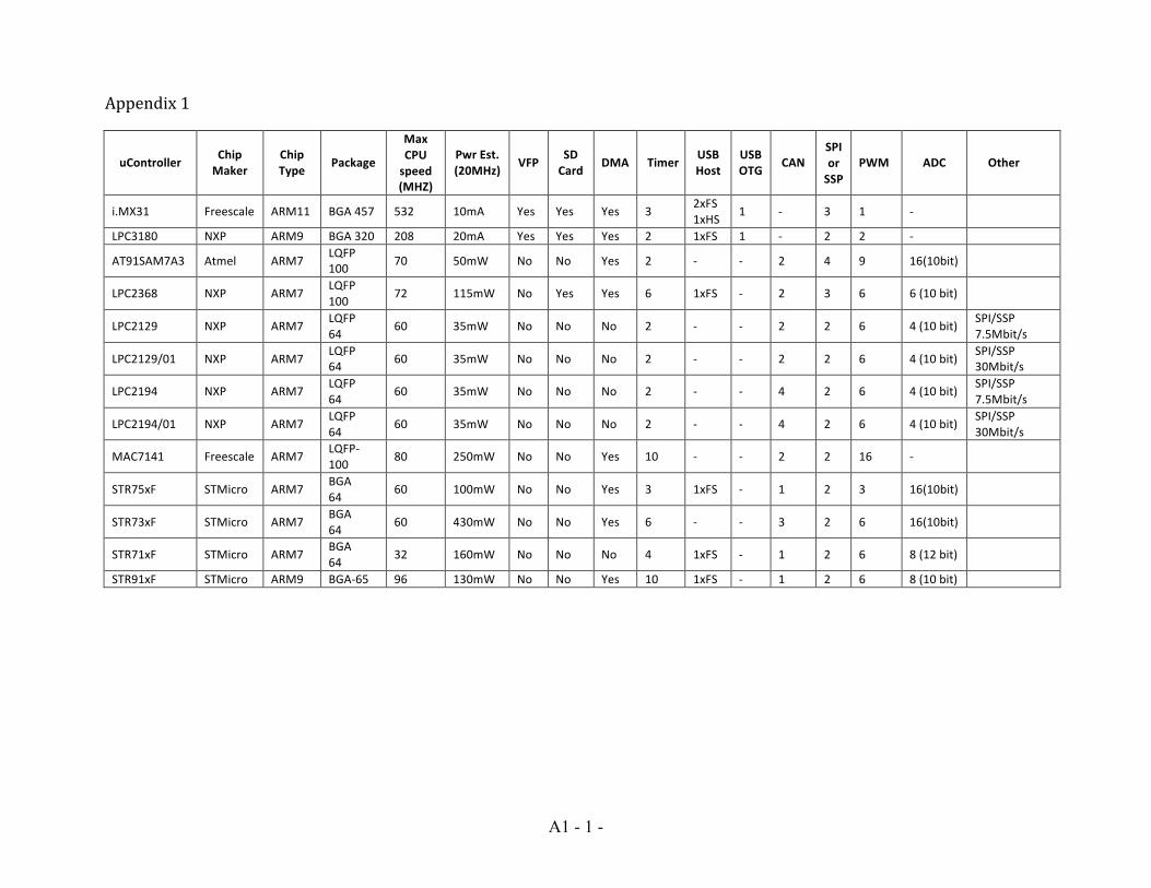
4. Short-listing Microcontrollers
There is a huge assortment of microcontrollers available in the market today with many
designed to suit different industries such as the automotive industry and the portable
electronics industry. Based on the requirements of the Multiple Microcontroller
Electronic Control System, we are able to shortlist a couple of potential microcontrollers
available on the market. This project will take the opportunity to test and use the
microcontrollers from the shortlist during the evaluation of protocols.
Due to the need to maintain low power consumption while maintaining the use of a 32bit
microcontroller with a wide array of tools and functionality, this project would focus on
using ARM microcontrollers. Moreover, with the wide support available for ARM
controllers, using ARM microcontrollers would be suitable for the research lab. The
ARM processor architecture is a 32-bit Reduced Instruction Set Computer (RISC)
processor developed by ARM Limited that is used widely in a number of embedded
designs. Due to their low power consumption, this processor architecture is very
dominant in the mobile electronics market. Currently, the ARM family of processors
accounts for approximately 75% of all embedded 32-bit CPUs, making one of the most
widely used computer architectures in the world.
The shortlisted microcontrollers are chosen based on the following rubric.
• The microcontroller would have the ARM architecture due to the need for low
power consumption as mentioned above.

- #$ -"
• Compute and compare the estimate of power consumption per unit cycle of the
microcontroller core. For this criterion, a simple approach would be finding the
hypothetical power consumption if the microcontroller speed is 20MHz.
• Compare the maximum microcontroller speed, to estimate its computing capability
• List support peripherals and functionality
o Vectored Floating Point (VFP) Unit: for fast floating point calculations
o SD Card interface: for information logging purposes
o Direct Memory Access: support for communication protocol
o Serial Peripheral Interface (SPI): support for communication protocol
o Universal Serial Bus (USB): support for communication protocol
o Controller Area Network (CAN): support for communication protocol
o Number of Timers
o Number of PWMs
o Number of Analog to Digital Converters (ADC)
The shortlisted microcontrollers are shown in Appendix 1.
- #% -"
5. Evaluating Protocols
Choosing the right protocols for use to communicate between the various
microcontrollers is important. The suitable protocols would need to not only have the
capacity to support the amount of data flow throughout the network, but also have
reasonable software overhead so as not to overwhelm the microcontroller that it is on.
This phase of evaluating different protocols for their suitability is aimed at choosing a
communications protocol for data transfer between the main microcontroller and
communications microcontroller, as well as a communications protocol for data transfer
between the communications microcontroller and the various low level microcontrollers.
The reason for dividing the protocol selection to two different parts is to allow for
flexibility. There is, however, a possibility that a single communications protocol is
suitable to handle the data flow between the main microcontroller and the various low
level microcontrollers.
It is also important to keep in mind that it is subject to the availability of the protocols on
viable microcontrollers. A particular protocol can potentially be evaluated to be optimal,
but if it were not implementable on a viable microcontroller, it would be unsuitable for
this project.
To evaluate the communication protocols, the testing and analysis would be carried out
by using evaluation boards containing one of the shortlisted microcontrollers which
would be used to build a test set up. The IAR Embedded Workbench KickStart Edition
from IAR systems is used to program the microcontrollers.

- #& -"
The evaluation process would comprise the following 3 communications protocol
1. Controller Area Network (CAN-bus)
2. Universal Serial Bus (USB)
3. Serial Peripheral Interface (SPI) with Direct Memory Access (DMA)
5.1. Controller Area Network (CAN-Bus)
5.1.1. Overview
CAN-Bus is a computer network protocol and a bus standard designed for devices to
communicate within the network without the need of a host computer. Intel Corporation
and Bosch jointly developed CAN-Bus in 1988 and it was specifically targeted for
automotive applications. Figure 4 shown below illustrates a high level view of a typical
CAN-Bus network.
Figure 4: High Level View of a Typical CAN-Bus network
The CAN-Bus protocol has the following characteristics:
- #' -"
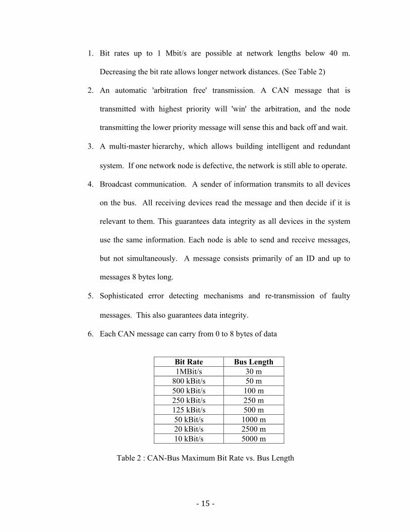
1. Bit rates up to 1 Mbit/s are possible at network lengths below 40 m.
Decreasing the bit rate allows longer network distances. (See Table 2)
2. An automatic 'arbitration free' transmission. A CAN message that is
transmitted with highest priority will 'win' the arbitration, and the node
transmitting the lower priority message will sense this and back off and wait.
3. A multi!master hierarchy, which allows building intelligent and redundant
system. If one network node is defective, the network is still able to operate.
4. Broadcast communication. A sender of information transmits to all devices
on the bus. All receiving devices read the message and then decide if it is
relevant to them. This guarantees data integrity as all devices in the system
use the same information. Each node is able to send and receive messages,
but not simultaneously. A message consists primarily of an ID and up to
messages 8 bytes long.
5. Sophisticated error detecting mechanisms and re!transmission of faulty
messages. This also guarantees data integrity.
6. Each CAN message can carry from 0 to 8 bytes of data
Bit Rate Bus Length
1MBit/s 30 m
800 kBit/s 50 m
500 kBit/s 100 m
250 kBit/s 250 m
125 kBit/s 500 m
50 kBit/s 1000 m
20 kBit/s 2500 m
10 kBit/s 5000 m
Table 2 : CAN-Bus Maximum Bit Rate vs. Bus Length
- #( -"
Although the CAN bus standard specifies that the maximum bit rate is 1Mbit per second,
there are CAN bus transceivers available on the market which support up to 2Mbit per
second. To be able to use them, however, the bus length has to be significantly shorter
then 30m. Although the rate of a single CAN bus does not meet the system
requirements, it is possible to set up a couple of CAN bus networks in parallel to obtain
the required bandwidth. This approach is possible as many microcontrollers have
multiple CAN bus ports on them. The automotive industry has also been using multiple
CAN bus networks in parallel to over come the lack of bandwidth of a single CAN bus
network.
5.1.2. Potential
It is easy to see that the potential use of this communications protocol would be in
facilitating the data flow between the communications microcontroller and the low level
microcontroller. As the protocol is that of broadcast communication, every
microcontroller in the CAN-Bus network would be able to listen in on what is being
transmitted. This can be crucial as the communications microcontroller would only need
to send information meant for multiple low level microcontrollers only once, rather than
sending the same data multiple times, wasting bandwidth.
- #) -"
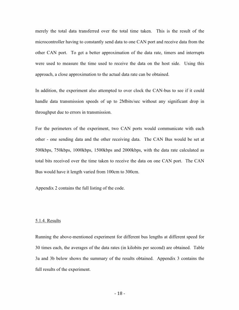
5.1.3. Experimental Setup and Testing
For evaluating the CAN-Bus protocol, the evaluation board for MAC7111
microcontroller was used. Figure 5 shows the picture of the MAC7111 evaluation board.
The MAC7111 microcontroller is from Freescale and it was chosen as it is an ARM7
with relatively low power consumption and it had 4 CAN-Bus ports.
Figure 5 : MAC7111 Low Cost Evaluation Board
(obtained from www.freescale.com)
To test the CAN-Bus protocol, 2 of the CAN-Bus ports were wired together and data was
sent through one port and received on the other. The received data was checked against
the data sent to check for errors. The speed of the data transmission and the length of the
CAN-bus were varied to obtain the throughput of the CAN-Bus under various conditions.
It is important to note that similar to the evaluation of the USB protocol, since the test is
performed on a single microcontroller, the rate at which the data is transferred is not
- #* -"
merely the total data transferred over the total time taken. This is the result of the
microcontroller having to constantly send data to one CAN port and receive data from the
other CAN port. To get a better approximation of the data rate, timers and interrupts
were used to measure the time used to receive the data on the host side. Using this
approach, a close approximation to the actual data rate can be obtained.
In addition, the experiment also attempted to over clock the CAN-bus to see if it could
handle data transmission speeds of up to 2Mbits/sec without any significant drop in
throughput due to errors in transmission.
For the perimeters of the experiment, two CAN ports would communicate with each
other - one sending data and the other receiving data. The CAN Bus would be set at
500kbps, 750kbps, 1000kbps, 1500kbps and 2000kbps, with the data rate calculated as
total bits received over the time taken to receive the data on one CAN port. The CAN
Bus would have it length varied from 100cm to 300cm.
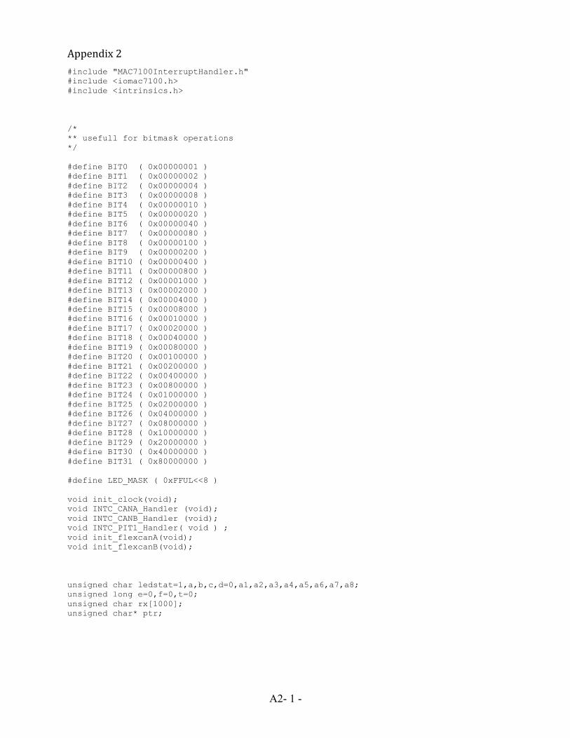
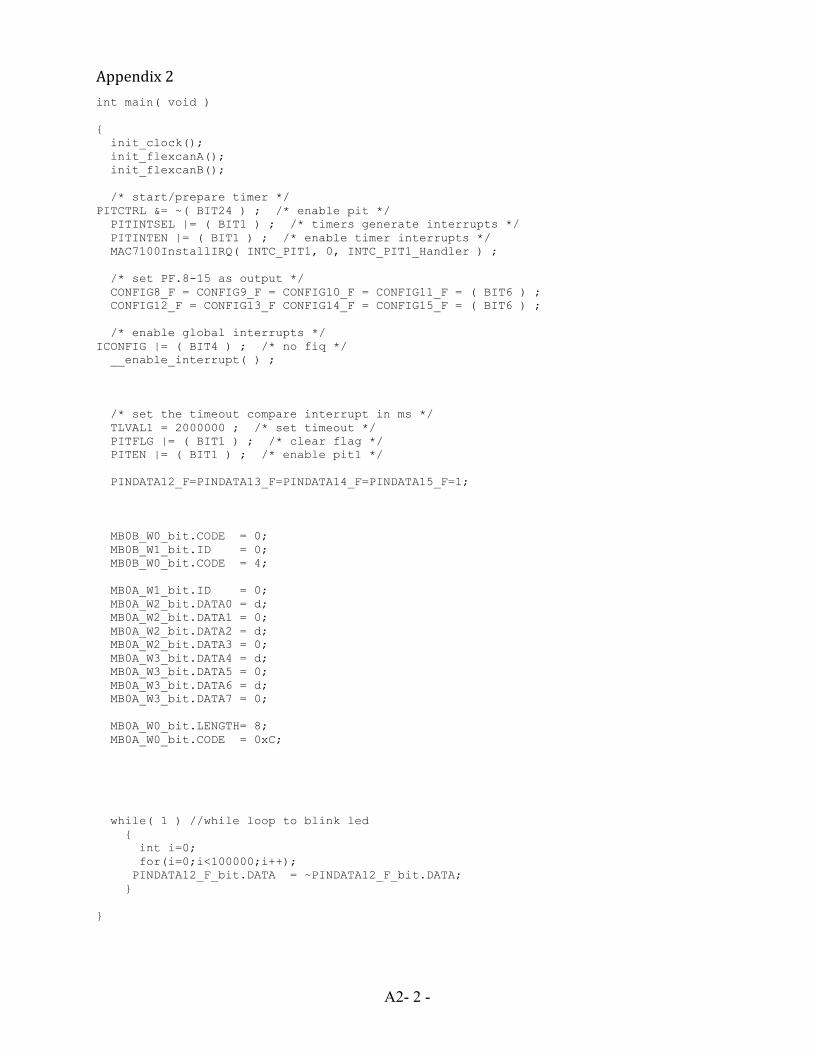
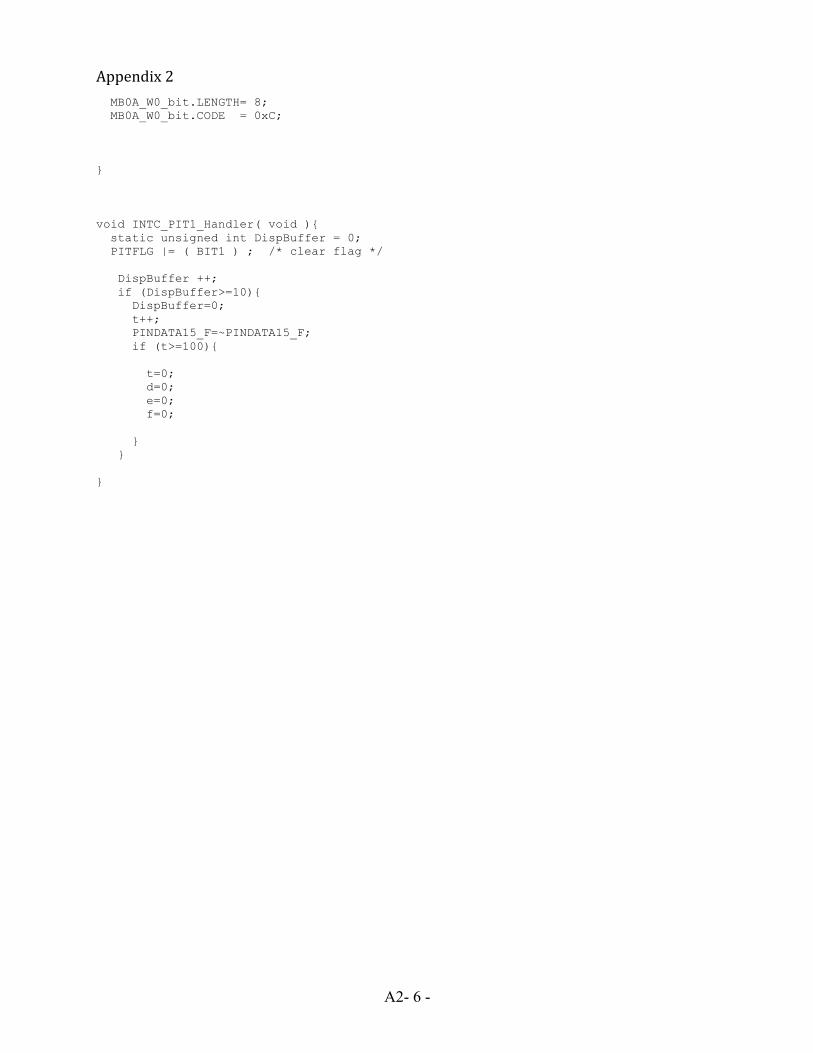
Appendix 2 contains the full listing of the code.
5.1.4. Results
Running the above-mentioned experiment for different bus lengths at different speed for
30 times each, the averages of the data rates (in kilobits per second) are obtained. Table
3a and 3b below shows the summary of the results obtained. Appendix 3 contains the
full results of the experiment.
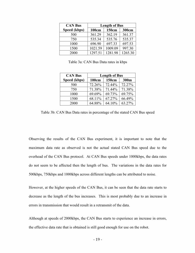
- #+ -"
Length of Bus CAN Bus
Speed (kbps) 100cm 150cm 300cm
500 361.29 362.19 361.37
750 535.34 535.76 535.37
1000 696.90 697.33 697.53
1500 1021.59 1009.09 997.30
2000 1297.51 1281.98 1265.30
Table 3a: CAN Bus Data rates in kbps
Length of Bus CAN Bus
Speed (kbps) 100cm 150cm 300m
500 72.26% 72.44% 72.27%
750 71.38% 71.44% 71.38%
1000 69.69% 69.73% 69.75%
1500 68.11% 67.27% 66.49%
2000 64.88% 64.10% 63.27%
Table 3b: CAN Bus Data rates in percentage of the stated CAN Bus speed
Observing the results of the CAN Bus experiment, it is important to note that the
maximum data rate as observed is not the actual stated CAN Bus speed due to the
overhead of the CAN Bus protocol. At CAN Bus speeds under 1000kbps, the data rates
do not seem to be affected then the length of bus. The variations in the data rates for
500kbps, 750kbps and 1000kbps across different lengths can be attributed to noise.
However, at the higher speeds of the CAN Bus, it can be seen that the data rate starts to
decrease as the length of the bus increases. This is most probably due to an increase in
errors in transmission that would result in a retransmit of the data.
Although at speeds of 2000kbps, the CAN Bus starts to experience an increase in errors,
the effective data rate that is obtained is still good enough for use on the robot.
- $, -"
5.2. Universal Serial Bus (USB)
5.2.1. Overview
The Universal Serial Bus (USB) is a widely used protocol, not only in personal
computers, but also in various different electronic gadgets. USB was designed to allow
many peripherals to be connected using a single standardized interface socket and to
improve the plug-and-play capabilities by allowing devices to be connected and
disconnected. The USB protocol has the following key features:
1. USB is a protocol that operates with a single host with multiple peripherals.
2. Up to 127 devices can connect to the host, either directly or by way of USB hubs.
3. Individual USB cables can run as long as 5 meters and with hubs, devices can be up
to 30 meters away from the host.
4. A USB cable has two wires for power and a twisted pair of wires to carry the data.
5. USB devices are hot-swappable.
6. The USB protocol is a widely supported with drivers available for most operating
systems.
In the analysis of the USB protocol, this part of the project will look at the
implementation of a full speed USB protocol in Bulk Mode.
The USB protocol is based on a system of endpoints that are established between the host
and the device during enumeration, with a maximum of 16 endpoints between the host
and each device. These endpoints can be viewed as “pipes” of data flow between the
host and the device. Figure 6 below illustrates the concept of endpoints in USB.

- $# -"
Figure 6: Concept of Endpoints in USB
(obtained from www.usb.org)
The USB full-speed protocol supports 3 different schemes for data transfers– Interrupt
transfers, Bulk transfers and Isochronous transfers. For interrupt transfers, the maximum
data rate is low as only 1 packet of information can be transferred at a time. As the name
suggests, interrupt transfers only occur when the data is received on the USB buffer and
an interrupt is asserted. As each USB frame is 1 millisecond in duration, the interrupt
that gets asserted is only be serviced once every millisecond. Since the maximum size of
a USB packet is 64 bytes, this implies that the maximum data rate of the USB interrupt
driven transfer is 512kbps. For Bulk transfers, the data rate is the highest among the
three schemes as it allows for multiple packets to be sent at a single time. The USB
protocol is capable of supporting up to 19 packets of 64 bytes for a bulk transfer,
allowing it to reach up to speeds close to the maximum of 12Mbps. For Isochronus
transfers, the data rate is unreliable as this scheme is meant for data streaming. It utilizes
- $$ -"
the remaining unused bandwidth to transfer data between the host and the device. Given
the above 3 schemes and time considerations, the analysis would only be performed using
the bulk transfers where the data rate is high.
5.2.2. Potential
There are 2 features of the USB protocol that makes it attractive as a protocol that this
project would use. Firstly, the data rate of the full speed USB is 12Mbps and it is
definitely high enough for the purposes of this project. Comparing with the analysis of
the MMECS model as discussed in the earlier section, the data rate more than satisfies the
needs of the model and it even provides capacity for further expansion. The second
feature is that the USB protocol is a widely supported protocol with drivers easily
available for most operating systems. This means that having a USB connection would
allow us to easily connect the robot up to a PC where testing and the development of the
robot itself would be greatly facilitated.
5.2.3. Experimental Setup and Testing
After some initial product and protocol research, the USB protocol is found to be rather
challenging to implement. Having to implement the whole USB state machine, together
with the error checking and timing issues would potentially occupy a significant amount
of time and set this project back for a considerable amount of time. In addition, a

- $% -"
significant number of the short listed microcontrollers as listed earlier in the report lack
USB functionality.
Given this situation, it was decided to perform the evaluation of the USB protocol using
an external USB controller that communicates with the microcontroller via the Serial
Peripheral Interface (SPI). This would be beneficial to the project as it would act as a
stepping stone to having a better understanding of USB as the USB controller takes care
of some of the lower level functions. Additionally, the interface between the
microcontroller and the USB controller is one that is rather easy to use.
The SPI-USB Controller that will be used for the evaluation of the USB protocol is the
MAX3421E from Maxim. The MAX3421E is a SPI-USB controller capable of Full
Speed USB transmissions. For testing purposes, the development board for the
MAX3421E as well as the MCB2130 development board from Keil was used. The
MCB2130 development board contains the LPC2138 microcontroller from NXP, while
the development board for the MAX3421E comes with both the MAX3421E and
MAX3420E (MAX3420E is the peripheral device version of the MAX3421E).
The approach to testing the USB protocol using the above-mentioned components is to
send data out through the peripheral side of the USB connection and receive data from
the host side of the connection.
It is important to note that since the test is performed on a single microcontroller, the rate
at which the data is transferred is not merely the total data transferred over the total time
taken. This is the result of the microcontroller having to constantly send data to the USB
- $& -"
device (MAX3420E) and receive data from the USB host (MAX3421E). To get a better
approximation of the data rate, timers and interrupts were used to measure the time used
to receive the data on the host side. Using this approach, the data rate on the full speed
USB connection can be measured.
Maxim provided an example base code to demonstrate the use of the development board
that they manufactured. The example code provided was originally for Keil MicroVision
software. The example code simulated the USB device as a Human Interface Device
(HID) in interrupt mode. The example code provide by Maxim can be found at Maxim’s
website
The code was ported over for use on IAR Embedded Workbench and modified for use to
evaluate the USB protocol and change it to bulk mode. All changes to the example code,
for ease of documentation purposes, were kept to the main code file – lpc2138.c, which
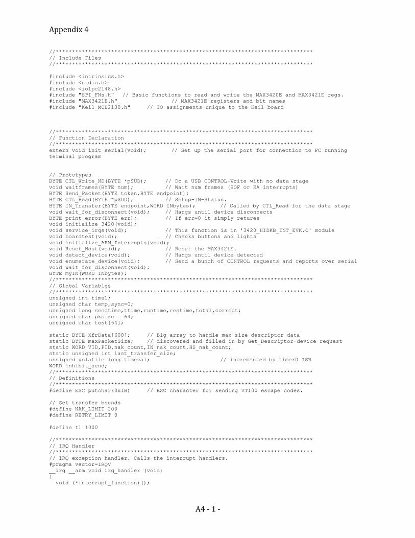
can be found in Appendix 4.
5.2.4. Results
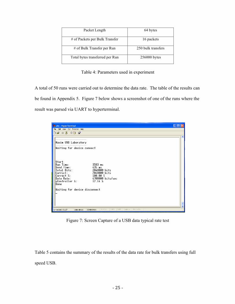
The data rate was measured for the bulk transfers over full speed USB. Table 4 contains
the parameters used to determine the data rate that can be achieved using the
MAX3241E.
- $' -"
Packet Length 64 bytes
# of Packets per Bulk Transfer 16 packets
# of Bulk Transfer per Run 250 bulk transfers
Total bytes transferred per Run 256000 bytes
Table 4: Parameters used in experiment
A total of 50 runs were carried out to determine the data rate. The table of the results can
be found in Appendix 5. Figure 7 below shows a screenshot of one of the runs where the
result was parsed via UART to hyperterminal.
Figure 7: Screen Capture of a USB data typical rate test
Table 5 contains the summary of the results of the data rate for bulk transfers using full
speed USB.
- $( -"
Data Rate (bps) % Correct uController Load
Average 4723920 100.00 12.54
Std Dev 147139 0.00 0.07
Table 5: Summary of Results for full speed USB bulk transfers
5.3 Serial Peripheral Interface (SPI) with Direct Memory Access (DMA)
5.3.1a. Overview - SPI
The Serial Peripheral Interface Bus or SPI bus is a synchronous serial data link standard
that operates in full duplex mode. This communications protocol consists of 4 wires –
Clock, Master In Slave Out (MISO) and Master Out Slave In (MOSI). Devices
communicate in a master/slave mode, allowing for multiple slaves with individual “Slave
Select” lines. Figure 8 below shows an example of a SPI bus with a single Master and a
single Slave.
Figure 8: SPI bus with a single Master and a single Slave
(obtained from www.embedded.com)
The SPI protocol is a very common protocol and it can be considered as a standard
- $) -"
feature in a wide range of microcontrollers. The maximum speeds of the SPI bus usually
vary between microcontrollers. The maximum speed is usually a factor of the CPU speed
of the SPI master microcontroller. For example, if a microcontroller has a CPU speed of
60Mhz, the possible SPI would be 60Mhz divided by a range of user definable values.
Hence, it is possible to have a fast SPI speed if a microcontroller with a fast CPU speed is
used.
5.3.1b. Overview - DMA
Direct memory access (DMA) is a feature that allows certain hardware subsystems within
the computer to access system memory for reading and writing independently of the main
core of the processor. DMA channels have the ability to transfer data to and from
devices with much less overhead than microcontrollers without a DMA channel.
Without DMA, the main core of the processor typically has to be occupied for the entire
time it's performing a transfer, while with DMA, the main core initiates the transfer, do
other operations while the transfer is in progress, and receive an interrupt from the DMA
controller once the operation has been done.
Figure 9 below shows the differences between data transfers that use DMA and those that
do not, for data that resides in Memory to the Serial Peripheral Interface (SPI). For the
purposes of this project, the data transfer between the main controller and the
communications controller will be using the Serial Peripheral Interface (SPI) protocol
and it will utilize DMA and implemented on the two respective controllers.

- $* -"
Figure 9: Differences in Data Transfers for SPI using DMA and not using DMA
5.3.2. Potential
The SPI with DMA implementation is especially useful for our purposes as it reduces the
load on the core of the main controller and free up more resources for the needs of the
robot. On the high level programming level, it would be straightforward as the process to
manage the dataflow would be setting the appropriate bits in the microcontroller to get
the Direct Memory Access re-started once every update interval. This also has an
additional benefit as it would reduce the processing load on the main microcontroller,
freeing up precious computing power.
!!
!"#$%&#!'()*!#$+!,-".!/%0+!%1!#$+!20%/+33%0!#42"/-554!$-3!#%!6+!%//&2"+7!1%0!#$+!+.#"0+!#",+!
"#83! 2+01%0,".9! -! #0-.31+0*! :$"5+! :"#$! '()*! #$+!,-".! /%0+! "."#"-#+3! #$+! #0-.31+0*! 7%! %#$+0!
%2+0-#"%.3!:$"5+!#$+!#0-.31+0! "3! ".!20%90+33*!-.7!0+/+";+!-.! ".#+00&2#!10%,!#$+!'()!/%.#0%55+0!
%./+!#$+!%2+0-#"%.!$-3!6++.!7%.+<!=$"3! "3!+32+/"-554!&3+1&5!1%0!%&0!2&02%3+3!-3! "#!0+7&/+3!#$+!
5%-7!%.!#$+!/%0+!%1!#$+!,-".!/%.#0%55+0!-.7!10++!&2!,%0+!0+3%&0/+3!1%0!#$+!.++73!%1!#$+!0%6%#<!!
>"9&0+!?!6+5%:!3$%:3!#$+!7"11+0+./+3!6+#:++.!7-#-!#0-.31+03!#$-#!&3+!'()!-.7!#$%3+!#$-#!7%!
.%#*!1%0!7-#-!#$-#!0+3"7+3!".!(+,%04!#%!#$+!@+0"-5!A+0"2$+0-5!B.#+01-/+!C@ABD!
>%0! #$+! 2&02%3+3! %1! #$"3! 0%6%#*! #$+! 7-#-! #0-.31+0! 6+#:++.! #$+! ,-".! /%.#0%55+0! -.7! #$+!
/%,,&."/-#"%.3!/%.#0%55+0!:"55!6+!&3".9!#$+!@+0"-5!A+0"2$+0-5!B.#+01-/+!C@ABD!20%#%/%5!-.7!"#!:"55!
&#"5"E+!'()!-.7!",25+,+.#+7!%.!#$+!#:%!0+32+/#";+!/%.#0%55+03<!!
!
>"9&0+!?F!'-#-!>5%:!6+#:++.!'()!+.-65+7!-.7!'()!7"3-65+7!#0-.31+03!
!
G<H!I%.#0%55+0!)0+-!J+#:%0K!L&3!CI)JD!
I)J! C-53%! 0+1+00+7! #%!-3!I)J6&3!%0!I)J!6&3D! "3!-!.+#:%0K!&3+7! ".!,-.4!+;+04"7-4!20%7&/#3!
/%.3"3#".9! %1! ,&5#"25+! ,"/0%/%.#0%55+03! #$-#! .++7! #%! /%,,&."/-#+! :"#$! +-/$! %#$+0<! ! =$+!
- $+ -"
5.3.3. Experimental Setup and Testing
The testing of SPI with DMA is carried out between the LPC3180 and the LPC2368, both
from NXP. The LPC3180 is an ARM9 microcontroller while the LPC2368 is an ARM7
microcontroller, both of which have Serial Peripheral Interface and are capable of
performing Direct Memory Access.
The reasons for using these 2 microcontrollers are two fold. Firstly, these two
microcontrollers as mentioned in the previous section, the ARM9 microcontrollers are a
class of more powerful microcontrollers as compared to ARM7 microcontrollers, using
the LPC3180 would allow us to gain experience in programming and working with
ARM9 microcontrollers. Secondly, using an ARM9 microcontroller as the SPI master
and the ARM7 microcontroller as the SPI slave closely parallels the potential use of this
communications protocol in the Multiple Microcontroller Electronic Control System. By
using a similar set up, possible problems or flaws that is currently unforeseen with the set
up can be uncovered.
The LPC3180 operates at a maximum of 208MHz and has a SPI capable of up to 52MHz,
while the LPC2368 operates at a maximum of 72MHz and has a SPI capable of up to
12MHz. To allow for a SPI speed that is implementable on both the microcontrollers, the
SPI for this analysis would be initially set at 8MHz.
The code for setting up the analysis on the LPC3180 and LPC2368 is found on Appendix
6 and 7 respectively.
- %, -"
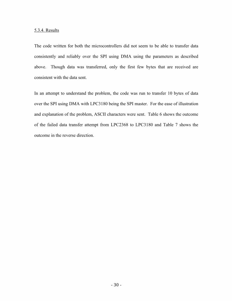
5.3.4. Results
The code written for both the microcontrollers did not seem to be able to transfer data
consistently and reliably over the SPI using DMA using the parameters as described
above. Though data was transferred, only the first few bytes that are received are
consistent with the data sent.
In an attempt to understand the problem, the code was run to transfer 10 bytes of data
over the SPI using DMA with LPC3180 being the SPI master. For the ease of illustration
and explanation of the problem, ASCII characters were sent. Table 6 shows the outcome
of the failed data transfer attempt from LPC2368 to LPC3180 and Table 7 shows the
outcome in the reverse direction.
- %# -"
Byte
Byte
Sent
Byte
Received
1 A A
2 B B
3 C C
4 D D
5 E 0
6 F 0
7 G 0
8 H 0
9 I 0
10 J 0
Table 6: Outcome of failed data transfer from LPC2368 to LPC3180
Byte
Byte
Sent
Byte
Received
1 A A
2 B B
3 C C
4 D D
5 E 0
6 F 0
7 G 0
8 H 0
9 I 0
10 J 0
Table 7: Outcome of failed data transfer from LPC3180 to LPC2368
Looking at the result of the failed data transfer, it can be suspected that the SPI on one of
the microcontrollers is unable to keep up with the data transfer. As a result, either the
SPI buffers overflows or underflows, resulting in only the first 4 bytes being successfully
transmitted.
- %$ -"
This issue was further investigated and it was found that the SPI and the DMA on the
LPC2368 was unable to keep up with the SPI speed of 8MHz. The same run was carried
out with the SPI at 2MHz and the data was successfully transferred.
Help was sought from the technical support from NXP to confirm the observations and it
was confirmed that the Direct Memory Access (DMA) controller was unable to keep up
the data transfers between the SPI buffers and the memory locations. The technical
support cited 2 explanations for the observations:
1. The LPC3180 is designed to run at a significantly higher CPU speed as compared
to the LPC2368. Hence, the DMA controller in the LPC3180 is able to keep up
with the data transfers, but not the LPC2368.
2. The SPI buffer in the LPC2368 is of length 2, while the SPI buffer in the LPC3180
is of length 56. Hence, the SPI buffer in the LPC3180 is able to store more data
before the SPI overflows. This is especially so since the SPI is operating at a high
speed.
Since most of the other ARM7 microcontrollers are similar in terms of computing power
as compared to the LPC2368, it is unlikely that the problem would be nonexistent if we
replace the LPC2368 with another ARM7 microcontroller. As a result, using SPI with
DMA is only possible within the constraints of this project to have a transfer speed within
the ballpark of about 2MHz.

- %% -"
Clearly, using SPI with DMA as a communications protocol does not meet the
requirements for this MMECS. Unlike the CAN Bus, although the SPI can operate in a
single master multiple slave setup, the master would have to poll each of the slave to send
or receive data that is associated each slave. This feature of the SPI places additional
load on the master and this would potentially be an issue for the microcontroller
6. Choosing Microcontrollers and Protocols
After short-listing the microcontrollers and evaluating the communications protocols, an
informed decision can be made with regards to choosing the appropriate microcontroller
and communication protocol.
For the communication protocols, the analysis revealed that using SPI with DMA does
not seem to be a viable option due to the inability of the DMA controller to keep up with
the speed of the data transmission.
The CAN Bus protocol seemed rather promising as the experiments showed that speeds
of up to 2000kbps were possible. Though the actual rate is slower due to the protocol
overhead, the extra bandwidth obtained by “overclocking” the CAN Bus would definitely
go a long way. Although the CAN Bus is comparatively slower in speeds as compared to
the other protocols analyzed, it is possible for the system to have multiple CAN Buses in
parallel to effectively have a higher data rate. This is possible as many microcontrollers,
- %& -"
as seen from the shortlist, have multiple CAN ports. It is important, however, to note that
the more powerful microcontrollers tend not to have CAN ports on them. As we can see
from the shortlist, the LPC3180 and i.MX31 microcontrollers do not have CAN ports, but
they are seemingly very attractive main microcontrollers for the project.
The full speed USB protocol that was analyzed is also very promising. From the results,
the analysis showed that it had sufficient bandwidth and it is possible for it to be
implemented using external controllers that interface with a host microcontroller via SPI.
Compared to the CAN bus, it would be almost equivalent in terms of data rate if 4 CAN
Buses were used in parallel. One downside to the USB protocol is the implementation of
the USB stack as well as its state machine. Just looking at the code used to setup the data
transfers between the host and device, it is clear that the computational power needed to
run the USB protocol is sizable. In addition, due to the complex nature of the USB
protocol, it might not be suitable to proceed with implementing a full scale USB protocol
along with the device drivers given the manpower and capability of the research lab at the
current point of time. Hence, USB might only suitable for implementation on a smaller
scale where it is possible to temporarily ignore some of the USB specifications.
Given the above analysis and results, the best implementation of the multiple
microcontroller electrical control system would be for the USB protocol to be used
between the main microcontroller and the communications controller and the CAN Bus
protocol over 4 separate but parallel networks would be used for communication between
the communications controller and the multiple low level controllers. The
communications controller would effectively act as a router to transmit data not only
- %' -"
between the low level microcontrollers and the main controller, but also between the low
level microcontrollers if the communicating low level microcontrollers are on separate
CAN Bus networks. As for the microcontrollers themselves, the following would be the
microcontrollers for the electronic control system.
• Main Microcontroller: i.MX31 from Freescale
• Communications Microcontroller: LPC2194/01 from NXP
• Low level Microcontroller: LPC2194/01 from NXP
In my opinion, this would be the most suitable implementation as it combines the
strengths of both the CAN Bus and USB protocols. Furthermore, the task of
implementing of the actual system would not be too overwhelming for the future student
researchers to continue work on.
One key reason for deciding on this implementation for the electronic control system is
also scalable. If there would be a future need to increase the capacity of the data
transmission between the microcontrollers, this implementation would easily allow for an
upgrade. Firstly, the i.MX31 supports both full speed USB as well as hi speed USB, if
the capacity for the full speed USB eventually becomes insufficient, a switch can be
made to the hi speed USB. By adding a hi-speed USB hub, the communications
microcontroller can be replicated to obtain multiple CAN Bus networks to support the
bandwidth as well. Although, the implementation of the USB protocol to communicate
from a singe host to multiple devices is not simple or trivial, there would be more time
between currently and the future for the USB protocol to be fully implemented.
- %( -"
7. Initial Progress in Building the MMECS
7.1. Setting Up Initial Base Code
As the microcontroller and the communication protocols have been chosen for the whole
system, the actual building of the system and programming of the microcontrollers to
support the communications protocols and their respective tasks would natural follow in
the design process. However, as mentioned in the introduction that the scope of this
project does not encompass the entirety of the process till the network-based electronic
communication system as ready as a “product” for use in the development of a robot,
other students researchers would have to continue on where this project left off.
In programming a microcontroller, especially if it is an unfamiliar microcontroller or a
new programming environment, there is always the initial set up of the project files,
linker files as well as other settings. This can possibly be a steep learning curve. Hence,
if students were provided with a sample project with straightforward no-frills code, they
would not have to worry about getting the settings correct and understanding the sample
code. The students would be able to begin the programming task almost immediately,
saving effort and time.
7.1.1. Details of Initial Base Code
The initial base code written consists of very basic elements to get a typical student
programmer started as soon as possible. The code accomplishes the following:
- %) -"
• Initialize the Phase Lock Loop in the microcontroller so the user can easily change
the CPU speeds by changing variables
• Initialize the Vectored Interrupt Controller in the code to handle interrupts
• Initialize a timer and its interrupt. This acts more as an example to initialize
interrupts on the microcontroller.
• Toggle an output. This acts more as a visual cue to the user so that they would
know that the microcontroller is running the code.
Instructions on how to change key settings in the project files are also included as
comments in the code. The full listing of the example code can be found in Appendix 8.
7.1.2. Functional Description of Initial Base Code
The initial base code is a simple code that allows for a programmer to get started quickly.
This section of the report details the key portions of the code to allow for the user to
better understand the base code.
a) Header Files
//******************************************************************************* // Include Files //******************************************************************************* #include <inarm.h> #include <intrinsics.h> #include <iolpc2119.h> // THIS IS THE MICROCONTROLLER HEADER FILE !!!!
This portion of the code includes the necessary header files for the code to run in
the programming environment. The header files – inarm.h and intrinsics.h are
headers files to initialize various compilers specific macros and variables.
- %* -"
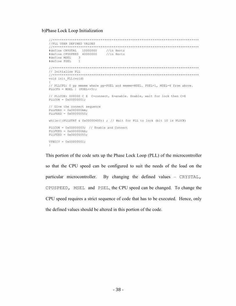
b) Phase Lock Loop Initialization
//******************************************************************************* //PLL USER DEFINED VALUES //******************************************************************************* #define CRYSTAL 10000000 //in Hertz #define CPUSPEED 40000000 //in Hertz #define MSEL 3 #define PSEL 1 //******************************************************************************* // Initialize PLL //******************************************************************************* void init_PLL(void) { // PLLCFG: 0 pp mmmmm where pp=PSEL and mmmmm=MSEL. PSEL=1, MSEL=4 from above. PLLCFG = MSEL | (PSEL<<5); // PLLCON: 000000 C E C=connect, E=enable. Enable, wait for lock then C+E PLLCON = 0x00000001; // Give the connect sequence PLLFEED = 0x000000AA; PLLFEED = 0x00000055; while(!(PLLSTAT & 0x00000400)) ; // Wait for PLL to lock (bit 10 is PLOCK) PLLCON = 0x00000003; // Enable and Connect PLLFEED = 0x000000AA; PLLFEED = 0x00000055; VPBDIV = 0x00000001; }
This portion of the code sets up the Phase Lock Loop (PLL) of the microcontroller
so that the CPU speed can be configured to suit the needs of the load on the
particular microcontroller. By changing the defined values – CRYSTAL,
CPUSPEED, MSEL and PSEL, the CPU speed can be changed. To change the
CPU speed requires a strict sequence of code that has to be executed. Hence, only
the defined values should be altered in this portion of the code.
- %+ -"
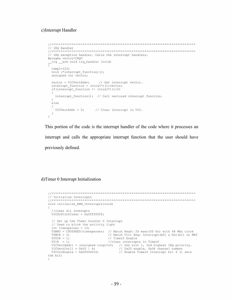
c) Interrupt Handler
//******************************************************************************* // IRQ Handler //******************************************************************************* // IRQ exception handler. Calls the interrupt handlers. #pragma vector=IRQV __irq __arm void irq_handler (void) { temp1=123; void (*interrupt_function)(); unsigned int vector; vector = VICVectAddr; // Get interrupt vector. interrupt_function = (void(*)())vector; if(interrupt_function != (void(*)())0) { interrupt_function(); // Call vectored interrupt function. } else { VICVectAddr = 0; // Clear interrupt in VIC. } }
This portion of the code is the interrupt handler of the code where it processes an
interrupt and calls the appropriate interrupt function that the user should have
previously defined.
d) Timer 0 Interrupt Initialization
//******************************************************************************* // Initialize Interrupts //******************************************************************************* void initialize_ARM_Interrupts(void) { //clear all interupts VICSoftIntClear = 0xffffffff; // Set up the Timer Counter 0 Interrupt // Used to blink the activity light int timespersec = 10; T0MR0 = CPUSPEED/timespersec; // Match Reg0: 20 msec(50 Hz) with 48 MHz clock T0MCR = 3; // Match Ctrl Reg: Interrupt(b0) & Rst(b1) on MR0 T0TCR = 1; // Timer0 Enable T0IR = 1; //clear interrupts in Timer0 VICVectAddr1 = (unsigned long)tc0; // Use slot 1, 2nd highest IRQ priority. VICVectCntl1 = 0x20 | 4; // 0x20 enable, 0x04 channel number VICIntEnable = 0x00000010; // Enable Timer0 Interrupt bit 4 (1 sets the bit) }
- !" -#
This portion of the code is the initialization of Timer0 as well as a compare match
interrupt. This would act as an example of a general approach for how to initialize
timers as well as how to set up interrupts.
7.2. Designing the Communications microcontroller
Based on the recommendations mentioned in the previous section, the communications
controller would essentially be a LPC2194/01 microcontroller that receives and transmits
data over USB and CAN Bus protocols. A printed circuit board (PCB) would be
designed to house the necessary components and circuits to function as a bridge between
the main microcontroller and the low level microcontrollers.
The following are the rough list key of parts needed for the design on the
communications circuit board:
• LPC2194/01 -microcontroller
• MAX3421E -SPI to USB controller
• CAN transceivers -to use the CAN bus protocol
• JTAG connection -for programming
• LEDS -as visual indicators
• Switching Power Regulators -to step down the power for use on the board
The schematic for the design of the communications circuit board is attached as
Appendix 9. However, as some of the actual components are currently still being tested
by other members of the trace layout of the communications board is placed on hold until
all testing of components are complete.
- &# -"
8. Conclusion
After performing the analysis of the MMECS, shortlisting microcontrollers, as well as the
evaluation of the various communications protocols, this project arrived at a
recommendation for the MMECS. The recommendation is a follows
• Microcontrollers
o Main Microcontroller: i.MX31 from Freescale
o Communications Microcontroller: LPC2194/01 from NXP
o Low Level Microcontroller: LPC2194/01 from NXP
• Communication Protocols
o Main to Communications Full Speed USB
o Communications to Low Level CAN Bus
The recommendation takes into account not only the technical requirements of the
project, but it also considers the number of personnel and expertise so that the multiple
microcontroller electronic control system can be reasonably completed in time for use in
the next walking robot built. In addition, the nature of the design also allows for
upgradability for incremental changes to be made to the electronic control system over
time.
Some initial work has also been done in building the MMECS. The initial base code was
written to allow for more individuals to participate in building of the MMECS and the
schematic of the communications microcontroller is also done.
- !" -#
9. References
Original CAN Specification http://ww.can.bosch.com/docu/can2spec.pdf
CAN Official Website http://www.canbus.us/
USB Official Website http://www.usb.org
Freescale Company Website http://www.freescale.com
NXP Company Website http://www.nxp.com
Keil Company Website http://www.keil.com
IAR Systems Company Website http://www.iar.com
IAR Emdedded Kickstart User Guide ftp://ftp.iar.se/WWWfiles/arm/Guides/ouarm_13.pdf
LPC2000 Discussion Forum http://www.embeddedrelated.com/groups/lpc2000/1.php

Appendices
!
!
"##$%&'(!)!
A1 - 1 -!
!"#$%&#''(&)"*+,)
-./(&)
"*+,)
01,()2.3/.4()
-.5)
"26)
7,((8)
9-:;<)
2=&)>7%?))
9@A-:B<)CD2)
EF)
".&8)F-G) 0+H(&)
6EI)
:#7%)
6EI)
J0K)"GL)
E2M)
#&)
EE2)
2N-) GF") J%*(&)
!"#$%&' ()**+,-.*' /0#&&' 12/'345' 4%6' &78/' 9*+' 9*+' 9*+' %'6:(;'
&:<;'&' =' %' &' =' ''
>?@%&A7' B$?' /0#C' 12/'%67'' 67A' 678/' 9*+' 9*+' 9*+' 6' &:(;' &' =' 6' 6' =' ''
/DC&;/#5/%' /E8*.' /0#5'>F(?'
&77'57' 478G' BH' BH' 9*+' 6' =' =' 6' 3' C' &IJ&7K!EL'' ''
>?@6%IA' B$?' /0#5'>F(?'
&77'56' &&48G' BH' 9*+' 9*+' I' &:(;' =' 6' %' I' I'J&7'K!EL' ''
>?@6&6C' B$?' /0#5'>F(?''''
I3'I7' %48G' BH' BH' BH' 6' =' =' 6' 6' I' 3'J&7'K!EL'
;?MN;;?'
5"4#K!EN+'
>?@6&6CN7&' B$?' /0#5'>F(?'''''
I3'I7' %48G' BH' BH' BH' 6' =' =' 6' 6' I' 3'J&7'K!EL'
;?MN;;?'
%7#K!EN+'
>?@6&C3' B$?' /0#5'>F(?'''''
I3'I7' %48G' BH' BH' BH' 6' =' =' 3' 6' I' 3'J&7'K!EL'
;?MN;;?'
5"4#K!EN+'
>?@6&C3N7&' B$?' /0#5'>F(?'''''
I3'I7' %48G' BH' BH' BH' 6' =' =' 3' 6' I' 3'J&7'K!EL'
;?MN;;?'
%7#K!EN+'
#/@5&3&' ()**+,-.*' /0#5'>F(?=
&77'A7' 6478G' BH' BH' 9*+' &7' =' =' 6' 6' &I' =' ''
;D054:(' ;D#!,)H' /0#5'12/'''''
I3'I7' &778G' BH' BH' 9*+' %' &:(;' =' &' 6' %' &IJ&7K!EL' ''
;D05%:(' ;D#!,)H' /0#5'12/'''''
I3'I7' 3%78G' BH' BH' 9*+' I' =' =' %' 6' I' &IJ&7K!EL' ''
;D05&:(' ;D#!,)H' /0#5'12/'''''
I3'%6' &I78G' BH' BH' BH' 3' &:(;' =' &' 6' I' A'J&6'K!EL' ''
;D0C&:(' ;D#!,)H' /0#C' 12/=I4' CI' &%78G' BH' BH' 9*+' &7' &:(;' =' &' 6' I' A'J&7'K!EL' ''
!
!
"##$%&'(!)!
A2- 1 -!
#include "MAC7100InterruptHandler.h" #include <iomac7100.h> #include <intrinsics.h> /* ** usefull for bitmask operations */ #define BIT0 ( 0x00000001 ) #define BIT1 ( 0x00000002 ) #define BIT2 ( 0x00000004 ) #define BIT3 ( 0x00000008 ) #define BIT4 ( 0x00000010 ) #define BIT5 ( 0x00000020 ) #define BIT6 ( 0x00000040 ) #define BIT7 ( 0x00000080 ) #define BIT8 ( 0x00000100 ) #define BIT9 ( 0x00000200 ) #define BIT10 ( 0x00000400 ) #define BIT11 ( 0x00000800 ) #define BIT12 ( 0x00001000 ) #define BIT13 ( 0x00002000 ) #define BIT14 ( 0x00004000 ) #define BIT15 ( 0x00008000 ) #define BIT16 ( 0x00010000 ) #define BIT17 ( 0x00020000 ) #define BIT18 ( 0x00040000 ) #define BIT19 ( 0x00080000 ) #define BIT20 ( 0x00100000 ) #define BIT21 ( 0x00200000 ) #define BIT22 ( 0x00400000 ) #define BIT23 ( 0x00800000 ) #define BIT24 ( 0x01000000 ) #define BIT25 ( 0x02000000 ) #define BIT26 ( 0x04000000 ) #define BIT27 ( 0x08000000 ) #define BIT28 ( 0x10000000 ) #define BIT29 ( 0x20000000 ) #define BIT30 ( 0x40000000 ) #define BIT31 ( 0x80000000 ) #define LED_MASK ( 0xFFUL<<8 ) void init_clock(void); void INTC_CANA_Handler (void); void INTC_CANB_Handler (void); void INTC_PIT1_Handler( void ) ; void init_flexcanA(void); void init_flexcanB(void); unsigned char ledstat=1,a,b,c,d=0,a1,a2,a3,a4,a5,a6,a7,a8; unsigned long e=0,f=0,t=0; unsigned char rx[1000]; unsigned char* ptr;
!
"##$%&'(!)!
A2- 2 -!
int main( void ) { init_clock(); init_flexcanA(); init_flexcanB(); /* start/prepare timer */ PITCTRL &= ~( BIT24 ) ; /* enable pit */ PITINTSEL |= ( BIT1 ) ; /* timers generate interrupts */ PITINTEN |= ( BIT1 ) ; /* enable timer interrupts */ MAC7100InstallIRQ( INTC_PIT1, 0, INTC_PIT1_Handler ) ; /* set PF.8-15 as output */ CONFIG8_F = CONFIG9_F = CONFIG10_F = CONFIG11_F = ( BIT6 ) ; CONFIG12_F = CONFIG13_F CONFIG14_F = CONFIG15_F = ( BIT6 ) ; /* enable global interrupts */ ICONFIG |= ( BIT4 ) ; /* no fiq */ __enable_interrupt( ) ; /* set the timeout compare interrupt in ms */ TLVAL1 = 2000000 ; /* set timeout */ PITFLG |= ( BIT1 ) ; /* clear flag */ PITEN |= ( BIT1 ) ; /* enable pit1 */ PINDATA12_F=PINDATA13_F=PINDATA14_F=PINDATA15_F=1; MB0B_W0_bit.CODE = 0; MB0B_W1_bit.ID = 0; MB0B_W0_bit.CODE = 4; MB0A_W1_bit.ID = 0; MB0A_W2_bit.DATA0 = d; MB0A_W2_bit.DATA1 = 0; MB0A_W2_bit.DATA2 = d; MB0A_W2_bit.DATA3 = 0; MB0A_W3_bit.DATA4 = d; MB0A_W3_bit.DATA5 = 0; MB0A_W3_bit.DATA6 = d; MB0A_W3_bit.DATA7 = 0; MB0A_W0_bit.LENGTH= 8; MB0A_W0_bit.CODE = 0xC; while( 1 ) //while loop to blink led { int i=0; for(i=0;i<100000;i++); PINDATA12_F_bit.DATA = ~PINDATA12_F_bit.DATA; } }

!
"##$%&'(!)!
A2- 3 -!
void init_clock(void){ /* Set PLL multiplication factor */ SYNR = 4; //40Mhz REFDV = 1; /* Configure PLL */ PLLCTL_bit.CME = 1; PLLCTL_bit.PLLON = 1; PLLCTL_bit.AUTO = 1; PLLCTL_bit.ACQ = 1; PLLCTL_bit.SCME = 1; /* Wait for PLL to achieve lock */ while( (CRGFLG & 0x08) == 0); /* Switch system clocks over to PLL */ CLKSEL_bit.PLLSEL = 1; /* Configure interrupts */ CRGINT = 0; /* Configure BDM control register */ BDMCTL = 0; } void init_flexcanA(void){ //Set Pins G4 and G5 as Peripheral Pins CONFIG4_G_bit.MODE = 1; CONFIG5_G_bit.MODE = 1; //Set Control Register CTRLA = 0; CTRLA_bit.RJW = 3; CTRLA_bit.PSEG1 = 2;// CTRLA_bit.PSEG2 = 2;// CTRLA_bit.PROPSEG = 2;// CTRLA_bit.TSYN = 1; CTRLA_bit.PRESDIV = 0; CTRLA_bit.LBUF = 0; CTRLA_bit.CLK_SRC = 1; //CTRLA_bit.LPB = 1; //Enable Loop back Mod //Initialize All Message Buffers - in Use MB0A_W0_bit.CODE =8; MB0A_W0_bit.IDE =0; //Initialize All Message Buffers - 1-31 Not in Use MB1A_W0 =0; MB2A_W0 =0; MB3A_W0 =0; MB4A_W0 =0; MB5A_W0 =0; MB6A_W0 =0; MB7A_W0 =0; MB8A_W0 =0; MB9A_W0 =0; MB10A_W0 =0; MB11A_W0 =0; MB12A_W0 =0; MB13A_W0 =0; MB14A_W0 =0; MB15A_W0 =0; MB16A_W0 =0; MB17A_W0 =0; MB18A_W0 =0; MB19A_W0 =0; MB20A_W0 =0; MB21A_W0 =0; MB22A_W0 =0; MB23A_W0 =0; MB24A_W0 =0; MB25A_W0 =0; MB26A_W0 =0; MB27A_W0 =0; MB28A_W0 =0; MB29A_W0 =0; MB30A_W0 =0; MB31A_W0 =0;

!
"##$%&'(!)!
A2- 4 -!
//Acceptance Mask Bit RXGMASKA_bit.MI = 0;//all 0 in the mask (dont care) //Interupt Set up IMASKA = 0x00000000; //Interupt Mask for MB0 IFLAGA = 0xffffffff; //clear interupt //Installing Interupts MAC7100InstallIRQ( INTC_CAN_A_MB, 0, INTC_CANA_Handler) ; //Configuration Register MCRA_bit.MAXMB = 0xf; MCRA_bit.SUPV = 1; MCRA_bit.MDIS = 0; MCRA_bit.HALT = 0; PINDATA13_F=0; } void init_flexcanB(void){ //RX MB0 //Set Pins G6 and G7 as Peripheral Pins CONFIG6_G_bit.MODE = 1; CONFIG7_G_bit.MODE = 1; //Set Control Register CTRLB = 0; CTRLB_bit.RJW = 3; CTRLB_bit.PSEG1 = 2;// CTRLB_bit.PSEG2 = 2;// CTRLB_bit.PROPSEG = 2;// CTRLB_bit.TSYN = 1; CTRLB_bit.PRESDIV = 0; CTRLB_bit.LBUF = 0; CTRLB_bit.CLK_SRC = 1; //CTRLB_bit.LPB = 1; //Enable Loop back Mod //Initialize All Message Buffers - in Use MB0B_W0_bit.CODE =0; MB0B_W0_bit.IDE =0; //Initialize All Message Buffers - 1-31 Not in Use MB1B_W0 =0; MB2B_W0 =0; MB3B_W0 =0; MB4B_W0 =0; MB5B_W0 =0; MB6B_W0 =0; MB7B_W0 =0; MB8B_W0 =0; MB9B_W0 =0; MB10B_W0 =0; MB11B_W0 =0; MB12B_W0 =0; MB13B_W0 =0; MB14B_W0 =0; MB15B_W0 =0; MB16B_W0 =0; MB17B_W0 =0; MB18B_W0 =0; MB19B_W0 =0; MB20B_W0 =0; MB21B_W0 =0; MB22B_W0 =0; MB23B_W0 =0; MB24B_W0 =0; MB25B_W0 =0; MB26B_W0 =0; MB27B_W0 =0; MB28B_W0 =0; MB29B_W0 =0; MB30B_W0 =0; MB31B_W0 =0; //Acceptance Mask Bit RXGMASKB_bit.MI = 0;//all 0 in the mask (dont care) //Interupt Set up IMASKB = 0x00000001; //Interupt Mask for MB0 IFLAGB = 0xffffffff; //clear interupt

!
"##$%&'(!)!
A2- 5 -!
//Installing Interupts MAC7100InstallIRQ( INTC_CAN_B_MB, 1, INTC_CANB_Handler) ; //Configuration Register MCRB_bit.MAXMB = 0xf; MCRB_bit.SUPV = 1; MCRB_bit.MDIS = 0; MCRB_bit.HALT = 0; PINDATA14_F=0; } void INTC_CANA_Handler (void){ IFLAGA = 0xffffffff; //clear interupt a = MB0A_W0_bit.CODE; b = MB0A_W2_bit.DATA0; c = MB0A_W0_bit.TIME_STAMP; d = MB0A_W2_bit.DATA1; e = MB0A_W2_bit.DATA2; } void INTC_CANB_Handler (void){ IFLAGB = 0xffffffff;; //clear interupt a = MB0B_W0_bit.CODE; b = MB0B_W0_bit.TIME_STAMP; a1= MB0B_W2_bit.DATA0; a2= MB0B_W2_bit.DATA1; a3= MB0B_W2_bit.DATA2; a4= MB0B_W2_bit.DATA3; a5= MB0B_W3_bit.DATA4; a6= MB0B_W3_bit.DATA5; a7= MB0B_W3_bit.DATA6; a8= MB0B_W3_bit.DATA7; if (a1 == d && a3==d&& a5==d && a7==d) e++; else{ c=1; } f++; d++; if(d>200)d=0; MB0B_W0_bit.CODE = 0; MB0B_W1_bit.ID = 0; MB0B_W0_bit.CODE = 4; MB0A_W1_bit.ID = 0; MB0A_W2_bit.DATA0 = d; MB0A_W2_bit.DATA1 = 0; MB0A_W2_bit.DATA2 = d; MB0A_W2_bit.DATA3 = 0; MB0A_W3_bit.DATA4 = d; MB0A_W3_bit.DATA5 = 0; MB0A_W3_bit.DATA6 = d; MB0A_W3_bit.DATA7 = 0;
!
"##$%&'(!)!
A2- 6 -!
MB0A_W0_bit.LENGTH= 8; MB0A_W0_bit.CODE = 0xC; } void INTC_PIT1_Handler( void ){ static unsigned int DispBuffer = 0; PITFLG |= ( BIT1 ) ; /* clear flag */ DispBuffer ++; if (DispBuffer>=10){ DispBuffer=0; t++; PINDATA15_F=~PINDATA15_F; if (t>=100){ t=0; d=0; e=0; f=0; } } }

!""#$%&'()
!)(*(+(*
!""#$ !%"#$ &""#$ !""#$ !%"#$ &""#$ !""#$ !%"#$ &""#$ !""#$ !%"#$ &""#$ !""#$ !%"#$ &""#$
! ),-.,+ )/0.+, )/).+1 ,),.-+ ,),.1+ ,)).-/ /1-.1- /1,.+- /12.1/ +303.1, +33-.33 112.,+ +01/.0) +02-.44 +0/,.-1
' ),2.,0 )/,.33 ),2.,3 ,),./4 ,)+.2- ,)-.0, /1/.+, /1).14 /1-.01 +30).,+ +332.), 111.-, +011.31 +0-).0/ +0/0.0)
& )/).1- ),2.40 )/).4/ ,)).3/ ,)0.-0 ,),.,+ /1,./0 233.+) /1/.14 +30+.13 +331.-, 11-.+/ +01,.3/ +0-).34 +0//.0+
( )/4.// )/).4+ )/0./+ ,)-.1, ,)/.2, ,)-.3- /14./2 /1/.1- /12.13 +304.+4 +3+).)- 11/.23 +)33.03 +0-4./3 +0//.-1
% ),-.// )/0.32 ),-.,2 ,)0.-0 ,)/.// ,),.,3 /12.)- /1,.,, /14./+ +3+-.-, +33-.+4 112.)3 +01/.// +0-).-2 +0//.+3
) )/+.3) )/3.-1 )/0./- ,),.+0 ,)2.0, ,)/.3/ /1-.1/ /12.11 233.)) +300.+, +33/.,/ 11/.40 +011.31 +021.)+ +0/2.+3
* ),1.41 )/0.)0 )/0.+/ ,)4.4/ ,)2.2+ ,)2.3, /1/.+) 233.+2 /1-.10 +3+1.,) +331.22 111.)3 +012.2) +0-0.)) +0//.21
+ )/0./+ )/)./- )/+.33 ,)-.)0 ,)).2+ ,)/.14 /12.12 /12.4+ /1,.2) +304.40 +332.,/ +33+.), +011.,0 +0-+.-) +0/2.+0
, ),-.1/ )/+.-1 )/).,- ,)/./- ,),.+, ,)4./+ /1,.0) /12.)/ /11.3) +3+-.)2 +331.+1 11/.24 +01/.2/ +0-0.3- +0//.-4
!" )/4.)) )/+.+0 ),1.1/ ,),.-4 ,)/.30 ,)-.4, /1/.// /12.44 /1-.0/ +300.04 +3+3.11 11,.2/ +011.14 +0-,.,4 +0/).21
!! )/0.+2 )/4.1+ )/3.+/ ,)2.// ,)-.04 ,)/.2/ /1,.-1 /1/.00 /1,.02 +300.-, +33-.41 112.0+ +01,.33 +0-)./) +0/4.)+
!' )/3.)/ )/).44 )/+.-+ ,)).43 ,)/.33 ,)/.0, /1-.31 /11.2, /1,.,2 +303.42 +3++.,) 112.2- +011./- +0-).+/ +0/4.,3
!& )/,.0) )/4.-3 ),2.1+ ,)).2- ,)/./4 ,)+.-+ /1/.4- /12.02 233.,1 +30).21 +3+0./- 11,.,1 +01/.41 +0-3.)1 +0/+.--
!( ),1.-1 ),-.22 )/+.+, ,)).-4 ,)-.4) ,),.4) /1/./+ /11.,/ /11.2, +3+1.,2 +33-.13 11,.,3 +01,./+ +021.-+ +0/).42
!% )/3.4, )/3./+ )/+.)1 ,),.0- ,)2.41 ,)4./0 /11.+0 /12.)+ /1/.0- +304.)0 +33-.-, 112./+ +01-.34 +0-)./+ +0/4.,+
!) )/4.3- )/).02 ),1.21 ,)1.-3 ,)+.-- ,),.1/ /1-.40 /1/.3+ /12.1, +300.+1 +332.+3 114.3- +01/.,) +0-4.+2 +0/).)0
!* )/0.,0 ),1.-, )/4.34 ,)/.3/ ,)/.// ,),.12 /11.42 /1,.43 /11./- +30+.,, +332.4- 11-.13 +01-.-/ +022./0 +0/,.)3
!+ ),1.1- )/+.)0 )/0.24 ,)4.03 ,)4.// ,)).2- /1/.1/ /12.,3 /1,.03 +30+.3/ +33/.4, 11,.4/ +012.,4 +0-0./+ +0/,.,0
!, )/).)3 )/).3- )/+.1, ,)4./3 ,)2.2/ ,)4./1 /14.+4 /1-.3+ /1/.)4 +300.30 +331.04 11/.4/ +011.10 +0-).3/ +0/).+,
'" )/0.)3 )/4.44 )/3.,) ,)/.2/ ,)2.10 ,)).-) /1,.)2 /14.+3 233.)1 +3+1.2, +332./, 111.,/ +012.03 +0-3.+2 +0/0.,1
'! )/0.13 )/,.,3 )/3.0, ,)2.,- ,)2.,3 ,)4.)2 /1).)0 /1/.44 233.), +303.1, +3++.1/ 111.+- +012.-1 +0-+.20 +0/1.)/
'' )/).-- )/).43 )/0.,, ,)4.44 ,)).,4 ,)0.,+ /1-./0 /1,.,/ /1-.32 +3+1.-- +331.-1 11,.24 +012.12 +0-4.)0 +0/0.4)
'& )/0.43 )/0.)4 )/0.// ,),.00 ,),.4, ,),.-2 /1-./- /1,.42 /12.-, +30+.24 +33-.4+ 112.,, +01-.4- +0-).3, +0/-.2,
'( )/3.,, )/+.4, ),1.-, ,)/.41 ,)4.1) ,)).+/ /1,.12 /1-.22 /1/.44 +3+1.-, +332.,, 114.3- +01,.,1 +0-3.+3 +0/2.-+
'% )/3.)1 )/).)0 ),1.+/ ,),.02 ,)).-2 ,)0.,, /1/.-) /14.1/ 233.,+ +30+.// +3++.)1 111.,- +01/.+- +021.4, +0/).,0
') ),1.00 )/+.22 ),1.-- ,)).+2 ,)4.11 ,)/.03 /14.+4 /1,.-3 /14.0/ +30+.4- +33-.-- 11-.)) +01/.3/ +0-3./3 +0//.04
'* ),-.1, )/3.14 )/4.1) ,)4.,1 ,),.-1 ,)4.01 /1/.4/ 233.10 /14.++ +30).)) +33-.41 114.+0 +012.32 +0-0.24 +0//.42
'+ )/3.33 )/).42 )/0.,- ,)).)- ,)0./0 ,))./0 /1/.+/ 233.4/ /1,.,- +303.,1 +3+3.20 114.1/ +01,.1+ +0-3.), +0/).12
', )/3.21 ),1.++ )/+./) ,),.2) ,)/.2- ,)-.-4 233.,- 233.3, /1,./) +3+1.,2 +3+3.)+ 11-.23 +01,.1+ +0-3.14 +0//.),
&" ),1.,4 ),1.1+ )/+.)4 ,)0.+) ,)2.10 ,)/.)) /12.10 /1-.+- /1-.32 +304.1- +33,.21 111.)1 +011.+1 +0-).42 +0//.2)
&)!-', &)'-!, &)!-&* %&%-&( %&%-*) %&%-&* ),)-," ),*-&& ),*-%& !"'!-%, !"",-", ,,*-&" !',*-%! !'+!-,+ !')%-&"
'-!! !-,* !-+! !-+* !-,& !-+' !-*) !-,* '-"' !-** !-," !-," !-%+ !-,+ !-,+
./01
2345.678
9/15:80;7<
=>?5?@A
'"""CDE1*%"CDE1%""CDE1 !"""CDE1 !%""CDE1
!""#$%&'()(
!)(*(+(*(
//******************************************************************************* // Include Files //******************************************************************************* #include <intrinsics.h> #include <stdio.h> #include <iolpc2148.h> #include "SPI_FNs.h" // Basic functions to read and write the MAX3420E and MAX3421E regs. #include "MAX3421E.h" // MAX3421E registers and bit names #include "Keil_MCB2130.h" // IO assignments unique to the Keil board //******************************************************************************* // Function Declaration //******************************************************************************* extern void init_serial(void); // Set up the serial port for connection to PC running terminal program // Prototypes BYTE CTL_Write_ND(BYTE *pSUD); // Do a USB CONTROL-Write with no data stage void waitframes(BYTE num); // Wait num frames (SOF or KA interrupts) BYTE Send_Packet(BYTE token,BYTE endpoint); BYTE CTL_Read(BYTE *pSUD); // Setup-IN-Status. BYTE IN_Transfer(BYTE endpoint,WORD INbytes); // Called by CTL_Read for the data stage void wait_for_disconnect(void); // Hangs until device disconnects BYTE print_error(BYTE err); // If err=0 it simply retures void initialize_3420(void); void service_irqs(void); // This function is in '3420_HIDKB_INT_EVK.C' module void boardtest(void); // Checks buttons and lights void initialize_ARM_Interrupts(void); void Reset_Host(void); // Reset the MAX3421E. void detect_device(void); // Hangs until device detected void enumerate_device(void); // Send a bunch of CONTROL requests and reports over serial void wait_for_disconnect(void); BYTE myIN(WORD INbytes); //******************************************************************************* // Global Variables //******************************************************************************* unsigned int time1; unsigned char temp,sync=0; unsigned long sendtime,ttime,runtime,restime,total,correct; unsigned char pksize = 64; unsigned char test[64]; static BYTE XfrData[600]; // Big array to handle max size descriptor data static BYTE maxPacketSize; // discovered and filled in by Get_Descriptor-device request static WORD VID,PID,nak_count,IN_nak_count,HS_nak_count; static unsigned int last_transfer_size; unsigned volatile long timeval; // incremented by timer0 ISR WORD inhibit_send; //******************************************************************************* // Definitions //******************************************************************************* #define ESC putchar(0x1B) // ESC character for sending VT100 escape codes. // Set transfer bounds #define NAK_LIMIT 200 #define RETRY_LIMIT 3 #define t1 1000 //******************************************************************************* // IRQ Handler //******************************************************************************* // IRQ exception handler. Calls the interrupt handlers. #pragma vector=IRQV __irq __arm void irq_handler (void) { void (*interrupt_function)();
!""#$%&'()(
!)(*(+(*(
unsigned int vector; vector = VICVectAddr; // Get interrupt vector. interrupt_function = (void(*)())vector; if(interrupt_function != NULL) { interrupt_function(); // Call vectored interrupt function. } else { VICVectAddr = 0; // Clear interrupt in VIC. } } //******************************************************************************* // Interrupt Handlers //******************************************************************************* //Dummy interrupt handler, called as default in irqHandler() if no other //vectored interrupt is called. static void DefDummyInterrupt() { } // Timer Counter 0 Interrupt executes each 20ms @ 48 MHz CPU Clock // Increment counters timeval for general program use. // void tc0 (void) { if(time1 > 0 ){ time1--; } sendtime++; runtime++; T0IR = 1; // Clear interrupt flag VICVectAddr = 0; // Dummy write to indicate end of interrupt service // L6_OFF // for the scope } // Timer Counter 1 Interrupt executes each 50ms @ 48 MHz CPU Clock // Checks the start/stop button, clears inhibit_send if pressed. // Also increments blinkcount and blinks the D4 led when at limit. // void tc1 (void) { T1IR = 1; // Clear interrupt flag VICVectAddr = 0; // Dummy write to indicate end of interrupt service // L7_OFF // for the scope } // EINT0 Interrupt handler--MAX3420E INT pin void INT3420 (void) { service_irqs(); EXTINT = 1; // Clear EINT0 interrupt flag (b0) VICVectAddr = 0; // Dummy write to indicate end of interrupt service } // EINT2 Interrupt Handler--MAX3421E INT pin (not used, just an example) void INT3421 (void) { EXTINT = 4; // Clear EINT2 interrupt flag (b0) VICVectAddr = 0; // Dummy write to indicate end of interrupt service } //******************************************************************************* // Initialize Interrupts //******************************************************************************* void initialize_ARM_Interrupts(void) { // Set up the Timer Counter 0 Interrupt // Used to blink the activity light
!""#$%&'()(
!)(*(+(*(
T0MR0 = 48000;//960000; // Match Register 0: 20 msec(50 Hz) with 48 MHz clock T0MCR = 3; // Match Control Reg: Interrupt(b0) and Reset(b1) on MR0 T0TCR = 1; // Timer0 Enable VICVectAddr1 = (unsigned long)tc0; // Use slot 1, second highest vectored IRQ priority. VICVectCntl1 = 0x20 | 4; // 0x20 interrupt enable bit, 0x04 TIMER0 channel number VICIntEnable = 0x00000010; // Enable Timer0 Interrupt bit 4 (1 sets the bit) // Set up the Timer Counter 1 Interrupt // Used to check the send/stop button PB5 T1MR0 = 4800000; // Match Register 0: 100 msec (10Hz) with 48 MHz clock T1MCR = 3; // Match Control Reg: Interrupt(b0) and Reset(b1) on MR0 T1TCR = 1; // Timer1 Enable VICVectAddr3 = (unsigned long)tc1; // Use slot 3, lowest vectored IRQ priority in this app VICVectCntl3 = 0x20 | 5; // 0x20 interrupt enable bit, 0x05 TIMER5 channel number VICIntEnable = 0x00000020; // Enable Timer1 Interrupt bit 5 (1 sets the bit) // Set up the EINT0 (P0.16) interrupt (MAX3420E Interrupt pin) // EXTMODE |= 0x01; // EINT0 is edge-sensitive EXTPOLAR |= 0x01; // positive edge EXTINT = 1; // clear the IRQ which may have been set VICVectAddr0 = (unsigned long)INT3420; // Use slot 0, highest vectored IRQ priority. VICVectCntl0 = 0x20 | 14; // 0x20 interrupt enable bit, 14(D) is EINT0 channel number VICIntEnable = 0x00004000; // Enable EINT0 interrupt bit 14 (1 sets the bit) // Set up the EINT2 (P0.15) interrupt (MAX3421E Interrupt pin)--not used, just an example. // Set for pos-edge Hwreg(rPINCTL,(bmFDUPSPI|bmPOSINT)); //INTLEVEL=0, POSINT=1 for pos edge interrupt pin EXTMODE |= 0x04; // EINT2 is edge-sensitive EXTPOLAR |= 0x04; // positive edge EXTINT = 4; // clear the IRQ which may have been set VICVectAddr2 = (unsigned long)INT3421; // Use slot 2 VICVectCntl2 = 0x20 | 16; // 0x20 interrupt enable bit, 16(D) EINT2 channel number VICIntEnable = 0x00010000; // Enable EINT2 interrupt bit 16 (1 sets the bit) } //******************************************************************************* // Task Functions //******************************************************************************* void task1(void){ time1=t1; if(temp){L1_ON;temp=0;} else{L1_OFF;temp=1;} } //******************************************************************************* // Main Function //******************************************************************************* void main (void) { init_PLL(); init_IO(); init_serial(); initialize_ARM_Interrupts(); initialize_3420(); time1=t1; __enable_interrupt(); // INITIALIZE MAX3421 // Hwreg(rPINCTL,(bmFDUPSPI|bmPOSINT)); // MAX3421E: Full duplex mode, INTLEVEL=0, POSINT=1 for pos edge interrupt pin Reset_Host(); // Jan07_2008: Moved Reset_Host after MAX3421 is put in full duplex mode Pwreg(rIOPINS1,0x00); // all LEDS off Hwreg(rIOPINS1,0x00); // seven-segs off Hwreg(rIOPINS2,0x00); // and Vbus OFF (in case something already plugged in)
!""#$%&'()(
!)(*()(*(
// // Cycle power. This section was added after observing that some USB thumb drives can get // into a locked-up state that a USB bus reset does not clear. This behavior was observed // by starting this program with a thumb drive already plugged in. // time1=t1; // timeval clicks every 20 msec while(time1 > 500) ; VBUS_ON // Vbus back ON //Pwreg(rEPIEN,Prreg(rEPIEN)| bmIN3BAVIE); int i=0,cc=0; int qq=0; while(1){ ESC; printf("[2J"); // clear the VT100 screen ESC; printf("[H"); // reset cursor printf("--------------------\n"); printf("Maxim USB Laboratory\n"); printf("--------------------\n"); detect_device(); waitframes(200); // Some devices require this enumerate_device(); for(i=0;i<pksize;i++){test[i]=i;} for(i=0;i<600;i++){ XfrData[i]=0;} printf("Start\r\n"); ttime=0; runtime=0; total=0; correct=0; Pwritebytes(rEP2INFIFO, pksize, test); Pwreg(rEP2INBC,pksize); Pwritebytes(rEP2INFIFO, pksize, test); Pwreg(rEP2INBC,pksize); for(cc=0;cc<500;cc++){ //sendtime=0; qq=IN_Transfer(2,512); //ttime=ttime+sendtime; total+=last_transfer_size; for(i=0;i<512;i++){ if(XfrData[i]==i%64) correct++; } } restime=runtime; printf("Run Time:\t\t%d ms\r\n",restime); printf("Send Time:\t\t%d ms\r\n",ttime); printf("Total Bits:\t\t%d bits\r\n",total*8); printf("Correct:\t\t%d bits\r\n",correct*8); printf("Correct %%:\t\t%3.2f %%\r\n",((float)correct)/((float)total)*100); printf("Data Rate:\t\t%d bits/sec\r\n",total*8/ttime*1000); printf("uController %%:\t\t%3.2f %%\r\n",((float)ttime)/((float)restime)*100); printf("Done\r\n"); wait_for_disconnect(); } }
!""#$%&'()(
!)(*(+(*(
//******************************************************************************* // Reset Host //******************************************************************************* void Reset_Host(void) { Hwreg(rUSBCTL,bmCHIPRES); // chip reset This stops the oscillator Hwreg(rUSBCTL,0x00); // remove the reset while(!(Hrreg(rUSBIRQ) & bmOSCOKIRQ)) ; // hang until the PLL stabilizes } //******************************************************************************* // Detect Device //******************************************************************************* void detect_device(void) { int busstate; // Activate HOST mode & turn on the 15K pulldown resistors on D+ and D- Hwreg(rMODE,(bmDPPULLDN|bmDMPULLDN|bmHOST)); // Note--initially set up as a FS host (LOWSPEED=0) Hwreg(rHIRQ,bmCONDETIRQ); // clear the connection detect IRQ HL2_OFF; HL3_OFF; printf("Waiting for device connect\n\n"); do // See if anything is plugged in. If not, hang until something plugs in { Hwreg(rHCTL,bmSAMPLEBUS); // update the JSTATUS and KSTATUS bits busstate = Hrreg(rHRSL); // read them busstate &= (bmJSTATUS|bmKSTATUS); // check for either of them high } while (busstate==0); if (busstate==bmJSTATUS) // since we're set to FS, J-state means D+ high { // make the MAX3421E a full speed host Hwreg(rMODE,(bmDPPULLDN|bmDMPULLDN|bmHOST|bmSOFKAENAB)); readout(0xf); } if (busstate==bmKSTATUS) // K-state means D- high { // make the MAX3421E a low speed host Hwreg(rMODE,(bmDPPULLDN|bmDMPULLDN|bmHOST|bmLOWSPEED|bmSOFKAENAB)); readout(0x5); } } //******************************************************************************* // Enum Dev //******************************************************************************* void enumerate_device(void) { static BYTE HR,iCONFIG,iMFG,iPROD,iSERIAL; static WORD TotalLen,ix; static BYTE len,type,adr,pktsize; // SETUP bytes for the requests we'll send to the device static BYTE Set_Address_to_7[8] = {0x00,0x05,0x07,0x00,0x00,0x00,0x00,0x00}; static BYTE Get_Descriptor_Device[8] = {0x80,0x06,0x00,0x01,0x00,0x00,0x00,0x00}; static BYTE Get_Descriptor_Config[8] = {0x80,0x06,0x00,0x02,0x00,0x00,0x00,0x00}; // Get_Descriptor-String template. Code fills in idx at str[2]. static BYTE str[8] = {0x80,0x06,0x00,0x03,0x00,0x00,0x40,0x00}; // Issue a USB bus reset ;//printf("Issuing USB bus reset\n"); Hwreg(rHCTL,bmBUSRST); // initiate the 50 msec bus reset while(Hrreg(rHCTL) & bmBUSRST); // Wait for the bus reset to complete // Wait some frames before programming any transfers. This allows the device to recover from // the bus reset. waitframes(200); // Get the device descriptor.
!""#$%&'()(
!)(*(+(*(
maxPacketSize = 8; // only safe value until we find out Hwreg(rPERADDR,0); // First request goes to address 0 Get_Descriptor_Device[6]=8; // wLengthL Get_Descriptor_Device[7]=0; // wLengthH ;//printf("First 8 bytes of Device Descriptor "); HR = CTL_Read(Get_Descriptor_Device); // Get device descriptor into XfrData[] if(print_error(HR)) return; // print_error() does nothing if HRSL=0, returns the 4-bit HRSL. ;//printf("(%u/%u NAKS)\n",IN_nak_count,HS_nak_count); // Show NAK count for data stage/status stage maxPacketSize = XfrData[7]; for (ix=0; ix<last_transfer_size;ix++) ;//printf("%02X ",(BYTE*)XfrData[ix]); ;//printf("\n"); ;//printf("EP0 maxPacketSize is %02u bytes\n",maxPacketSize); // Issue another USB bus reset ;//printf("Issuing USB bus reset\n"); Hwreg(rHCTL,bmBUSRST); // initiate the 50 msec bus reset while(Hrreg(rHCTL) & bmBUSRST); // Wait for the bus reset to complete waitframes(200); // Set_Address to 7 (Note: this request goes to address 0, already set in PERADDR register). ;//printf("Setting address to 0x07\n"); HR = CTL_Write_ND(Set_Address_to_7); // CTL-Write, no data stage if(print_error(HR)) return; waitframes(30); // Device gets 2 msec recovery time Hwreg(rPERADDR,7); // now all transfers go to addr 7 // Get the device descriptor at the assigned address. Get_Descriptor_Device[6]=0x12; // fill in the real device descriptor length ;//printf("\nDevice Descriptor "); HR = CTL_Read(Get_Descriptor_Device); // Get device descriptor into XfrData[] if(print_error(HR)) return; ;//printf("(%u/%u NAKS)\n",IN_nak_count,HS_nak_count); ;//printf ("-----------------\n"); VID = XfrData[8] + 256*XfrData[9]; PID = XfrData[10]+ 256*XfrData[11]; iMFG = XfrData[14]; iPROD = XfrData[15]; iSERIAL = XfrData[16]; for (ix=0; ix<last_transfer_size;ix++) ;//printf("%02X ",(BYTE*)XfrData[ix]); ;//printf("\n"); ;//printf("This device has %u configuration\n",XfrData[17]); ;//printf("Vendor ID is 0x%04X\n",VID); ;//printf("Product ID is 0x%04X\n",PID); // str[2]=0; // index 0 is language ID string str[4]=0; // lang ID is 0 str[5]=0; str[6]=4; // wLengthL str[7]=0; // wLengthH HR = CTL_Read(str); // Get lang ID string if (!HR) // Check for ACK (could be a STALL if the device has no strings) { ;//printf("\nLanguage ID String Descriptor is "); for (ix=0; ix<last_transfer_size;ix++) ;//printf("%02X ",(BYTE*)XfrData[ix]); str[4]=XfrData[2]; // LangID-L str[5]=XfrData[3]; // LangID-H str[6]=255; // now request a really big string } if(iMFG) { str[2]=iMFG; // fill in the string index from the device descriptor
!""#$%&'()(
!)(*(+(*(
HR = CTL_Read(str); // Get Manufacturer ID string ;//printf("\nManuf. string is \""); for (ix=2; ix<last_transfer_size;ix+=2) ;//printf("%c",(BYTE*)XfrData[ix]); ;//printf("\"\n"); } else ;//printf("There is no Manuf. string\n"); if(iPROD) { str[2]=iPROD; HR = CTL_Read(str); // Get Product ID string ;//printf("Product string is \""); for (ix=2; ix<last_transfer_size;ix+=2) ;//printf("%c",(BYTE*)XfrData[ix]); ;//printf("\"\n"); } else ;//printf("There is no Product string\n"); if(iSERIAL) { str[2]=iSERIAL; HR = CTL_Read(str); // Get Serial Number ID string ;//printf("S/N string is \""); for (ix=2; ix<last_transfer_size;ix+=2) ;//printf("%c",(BYTE*)XfrData[ix]); ;//printf("\"\n"); } else ;//printf("There is no Serial Number"); // Get the 9-byte configuration descriptor ;//printf("\n\nConfiguration Descriptor "); Get_Descriptor_Config[6]=9; // fill in the wLengthL field Get_Descriptor_Config[7]=0; // fill in the wLengthH field HR = CTL_Read(Get_Descriptor_Config); // Get config descriptor into XfrData[] if(print_error(HR)) return; ;//printf("(%u/%u NAKS)\n",IN_nak_count,HS_nak_count); ;//printf ("------------------------\n"); for (ix=0; ix<last_transfer_size;ix++) ;//printf("%02X ",(BYTE*)XfrData[ix]); // Now that the full length of all descriptors (Config, Interface, Endpoint, maybe Class) // is known we can fill in the correct length and ask for the full boat. Get_Descriptor_Config[6]=XfrData[2]; // LengthL Get_Descriptor_Config[7]=XfrData[3]; // LengthH HR = CTL_Read(Get_Descriptor_Config); // Get config descriptor into XfrData[] ;//printf("\nFull Configuration Data"); for (ix=0; ix<last_transfer_size;ix++) { if((ix&0x0F)==0) printf("\n"); // CR every 16 numbers ;//printf("%02X ",(BYTE*)XfrData[ix]); } iCONFIG = XfrData[6]; // optional configuration string ;//printf("\nConfiguration %01X has %01X interface",XfrData[5],XfrData[4]); if (XfrData[4]>1) printf("s"); ;//printf("\nThis device is "); if(XfrData[7] & 0x40) ;//printf("self-powered\n"); else ;//printf("bus powered and uses %03u milliamps\n",XfrData[8]*2); // // Parse the config+ data for interfaces and endpoints. Skip over everything but // interface and endpoint descriptors. // TotalLen=last_transfer_size;;//printf("%d\r\n",TotalLen); ix=0; // do
!""#$%&'()(
!)(*(+(*(
// { // len=XfrData[ix]; // length of first descriptor (the CONFIG descriptor) // type=XfrData[ix+1]; // adr=XfrData[ix+2]; // pktsize=XfrData[ix+4]; // // if(type==0x04) // Interface descriptor? // ;//printf("Interface %u, Alternate Setting %u has:\n",XfrData[ix+2],XfrData[ix+3]); // else if(type==0x05) // check for endpoint descriptor type // { // ;//printf("--Endpoint %u",(adr&0x0F)); // if (XfrData[ix+2]&0x80) ;//printf("-IN "); // else ;//printf("-OUT "); // ;//printf("(%02u) is type ",(BYTE)pktsize); // // switch(XfrData[ix+3]&0x03) // { // case 0x00: // ;//printf("CONTROL\n"); break; // case 0x01: // ;//printf("ISOCHRONOUS\n"); break; // case 0x02: // ;//printf("BULK\n"); break; // case 0x03: // ;//printf("INTERRUPT with a polling interval of %u msec.\n",XfrData[ix+6]); // } // } // ix += len; // point to next descriptor // ;//printf("%d\r\n",ix); // } // while (ix<TotalLen); // if(iCONFIG) { str[2]=iCONFIG; HR = CTL_Read(str); // Get Config string ;//printf("\nConfig string is \""); for (ix=2; ix<last_transfer_size;ix+=2) ;//printf("%c",(BYTE*)XfrData[ix]); ;//printf("\"\n"); } else;// printf("There is no Config string\n"); } //******************************************************************************* // Wait Frames //******************************************************************************* void waitframes(BYTE num) { BYTE k; Hwreg(rHIRQ,bmFRAMEIRQ); // clear any pending k=0; while(k!=num) // do this at least once { while(!(Hrreg(rHIRQ)& bmFRAMEIRQ)); Hwreg(rHIRQ,bmFRAMEIRQ); // clear the IRQ k++; } } //******************************************************************************* // Device Disconnect //******************************************************************************* void wait_for_disconnect(void) { printf("\nWaiting for device disconnect\n"); Hwreg(rHIRQ,bmCONDETIRQ); // clear the disconect IRQ while(!(Hrreg(rHIRQ) & bmCONDETIRQ)) ; // hang until this changes Hwreg(rMODE,bmDPPULLDN|bmDMPULLDN|bmHOST); // turn off frame markers
!""#$%&'()(
!)(*(+(*(
printf("\nDevice disconnected\n\n"); HL1_OFF HL4_OFF readout(0x00); } //******************************************************************************* // Print Error //******************************************************************************* BYTE print_error(BYTE err) { if(err) { printf(">>>>> Error >>>>> "); switch(err) { case 0x01: printf("MAX3421E SIE is busy "); break; case 0x02: printf("Bad value in HXFR register "); break; case 0x04: printf("Exceeded NAK limit"); break; case 0x0C: printf("LS Timeout "); break; case 0x0D: printf("FS Timeout "); break; case 0x0E: printf("Device did not respond in time "); break; case 0x0F: printf("Device babbled (sent too long) "); break; default: printf("Programming error %01X,",err); } } return(err); } // ----------------------------------------------------------------------------------- // Control-Write with no data stage. Assumes PERADDR is set and the SUDFIFO contains // the 8 setup bytes. Returns with result code = HRSLT[3:0] (HRSL register). // If there is an error, the 4 MSB's of the returned value indicate the stage 1 or 2. // ----------------------------------------------------------------------------------- BYTE CTL_Write_ND(BYTE *pSUD) { BYTE resultcode; Hwritebytes(rSUDFIFO,8,pSUD); // 1. Send the SETUP token and 8 setup bytes. Device should immediately ACK. resultcode=Send_Packet(tokSETUP,0); // SETUP packet to EP0 if (resultcode) return (resultcode); // should be 0, indicating ACK. // 2. No data stage, so the last operation is to send an IN token to the peripheral // as the STATUS (handshake) stage of this control transfer. We should get NAK or the // DATA1 PID. When we get the DATA1 PID the 3421 automatically sends the closing ACK. resultcode=Send_Packet(tokINHS,0); // This function takes care of NAK retries. if(resultcode) return (resultcode); // should be 0, indicating ACK. else return(0); } // ----------------------------------------------------------------------------------- // Send a packet. // ENTRY: PERADDR preset to the peripheral address. // EXIT: Result code. 0 indicates success. // 1. Launch the packet, wait for the host IRQ, reset the host IRQ. // 2. Examine the result code. // If NAK, re-send the packet up to NAK_LIMIT times. // If bus timeout (no response), re-send packet up to RETRY_LIMIT times. // Otherwise, return the result code: 0=success, nonzero=error condition. // ----------------------------------------------------------------------------------- BYTE Send_Packet(BYTE token,BYTE endpoint) { BYTE resultcode,retry_count; retry_count = 0; nak_count = 0; // while(1) // If the response is NAK or timeout, keep sending until either NAK_LIMIT or RETRY_LIMIT is reached. // Returns the HRSL code. { Hwreg(rHXFR,(token|endpoint)); // launch the transfer while(!(Hrreg(rHIRQ) & bmHXFRDNIRQ)); // wait for the completion IRQ Hwreg(rHIRQ,bmHXFRDNIRQ); // clear the IRQ
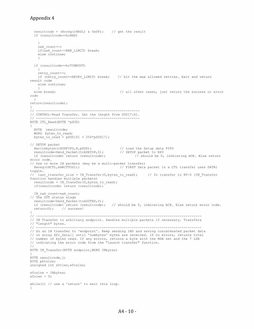
!""#$%&'()(
!)(*(+,(*(
resultcode = (Hrreg(rHRSL) & 0x0F); // get the result if (resultcode==hrNAK) { nak_count++; if(nak_count==NAK_LIMIT) break; else continue; } if (resultcode==hrTIMEOUT) { retry_count++; if (retry_count==RETRY_LIMIT) break; // hit the max allowed retries. Exit and return result code else continue; } else break; // all other cases, just return the success or error code } return(resultcode); } // ---------------------------------------------------- // CONTROL-Read Transfer. Get the length from SUD[7:6]. // ---------------------------------------------------- BYTE CTL_Read(BYTE *pSUD) { BYTE resultcode; WORD bytes_to_read; bytes_to_read = pSUD[6] + 256*pSUD[7]; // SETUP packet Hwritebytes(rSUDFIFO,8,pSUD); // Load the Setup data FIFO resultcode=Send_Packet(tokSETUP,0); // SETUP packet to EP0 if (resultcode) return (resultcode); // should be 0, indicating ACK. Else return error code. // One or more IN packets (may be a multi-packet transfer) Hwreg(rHCTL,bmRCVTOG1); // FIRST Data packet in a CTL transfer uses DATA1 toggle. // last_transfer_size = IN_Transfer(0,bytes_to_read); // In transfer to EP-0 (IN_Transfer function handles multiple packets) resultcode = IN_Transfer(0,bytes_to_read); if(resultcode) return (resultcode); IN_nak_count=nak_count; // The OUT status stage resultcode=Send_Packet(tokOUTHS,0); if (resultcode) return (resultcode); // should be 0, indicating ACK. Else return error code. return(0); // success! } // ----------------------------------------------------------------------------------- // IN Transfer to arbitrary endpoint. Handles multiple packets if necessary. Transfers // "length" bytes. // ----------------------------------------------------------------------------------- // Do an IN transfer to 'endpoint'. Keep sending INS and saving concatenated packet data // in array Xfr_Data[] until 'numbytes' bytes are received. If no errors, returns total // number of bytes read. If any errors, returns a byte with the MSB set and the 7 LSB // indicating the error code from the "launch transfer" function. // BYTE IN_Transfer(BYTE endpoint,WORD INbytes) { BYTE resultcode,j; BYTE pktsize; unsigned int xfrlen,xfrsize; xfrsize = INbytes; xfrlen = 0; while(1) // use a 'return' to exit this loop. {
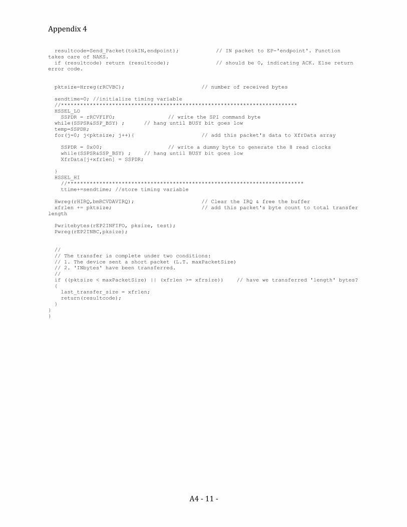
!""#$%&'()(
!)(*(++(*(
resultcode=Send_Packet(tokIN,endpoint); // IN packet to EP-'endpoint'. Function takes care of NAKS. if (resultcode) return (resultcode); // should be 0, indicating ACK. Else return error code. pktsize=Hrreg(rRCVBC); // number of received bytes sendtime=0; //initialize timing variable //************************************************************************** HSSEL_LO SSPDR = rRCVFIFO; // write the SPI command byte while(SSPSR&SSP_BSY) ; // hang until BUSY bit goes low temp=SSPDR; for(j=0; j<pktsize; j++){ // add this packet's data to XfrData array SSPDR = 0x00; // write a dummy byte to generate the 8 read clocks while(SSPSR&SSP_BSY) ; // hang until BUSY bit goes low XfrData[j+xfrlen] = SSPDR; } HSSEL_HI //************************************************************************** ttime+=sendtime; //store timing variable Hwreg(rHIRQ,bmRCVDAVIRQ); // Clear the IRQ & free the buffer xfrlen += pktsize; // add this packet's byte count to total transfer length Pwritebytes(rEP2INFIFO, pksize, test); Pwreg(rEP2INBC,pksize); // // The transfer is complete under two conditions: // 1. The device sent a short packet (L.T. maxPacketSize) // 2. 'INbytes' have been transferred. // if ((pktsize < maxPacketSize) || (xfrlen >= xfrsize)) // have we transferred 'length' bytes? { last_transfer_size = xfrlen; return(resultcode); } } }
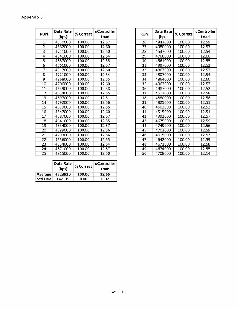
!""#$%&'()
A5 - 1 -
!"#$%&%'!%&('
)*+,-.'/011(2&
3/04&1055(1'
60%7!"#
$%&%'!%&('
)*+,-.'/011(2&
3/04&1055(1'
60%7
* +),---- *--.-- */.), /0 +1+2--- *--.-- */.)3/ +)0/--- *--.-- */.0- /, +31---- *--.-- */.),2 +,**--- *--.-- */.)- /1 +)2,--- *--.-- */.)++ +)+*--- *--.-- */.)+ /3 +,00--- *--.-- */.0-) +11,--- *--.-- */.)) 2- +)0*--- *--.-- */.))0 +)0*--- *--.-- */.), 2* +33,--- *--.-- */.)2, +)*,--- *--.-- */.0- 2/ +10,--- *--.-- */.),1 +,/*--- *--.-- */.)+ 22 +1-,--- *--.-- */.)+3 +101--- *--.-- */.)) 2+ +10+--- *--.-- */.0-*- +,-0--- *--.-- */.0- 2) +30/--- *--.-- */.)/** +0+3--- *--.-- */.)1 20 +31,--- *--.-- */.)/*/ +02+--- *--.-- */.)) 2, +0*/--- *--.-- */.)1*2 +13,--- *--.-- */.)* 21 +11---- *--.-- */.)1*+ +,3/--- *--.-- */.)0 23 +1/)--- *--.-- */.)**) +0,3--- *--.-- */.)) +- +0-/--- *--.-- */.)/*0 +)+,--- *--.-- */.0- +* +)*)--- *--.-- */.)**, +)1,--- *--.-- */.), +/ +33/--- *--.-- */.),*1 +0+*--- *--.-- */.)) +2 +0,)--- *--.-- */.)3*3 +12+--- *--.-- */.), ++ +,+3--- *--.-- */.)0/- +)13--- *--.-- */.)0 +) +,-2--- *--.-- */.)3/* +,32--- *--.-- */.)0 +0 +0*)--- *--.-- */.)2// +))0--- *--.-- */.)) +, +0+/--- *--.-- */.)3/2 +)2+--- *--.-- */.)+ +1 +0,*--- *--.-- */.)1/+ +1,*--- *--.-- */.), +3 +0,+--- *--.-- */.))/) +3*)--- *--.-- */.)- )- +,-1--- *--.-- */.*+
$%&%'!%&('
)*+,-.'/011(2&
3/04&1055(1'
60%7
89(1%:( ;<=>?=@ A@@B@@ A=BCCD&7'$(9 A;<A>? @B@@ @B@<
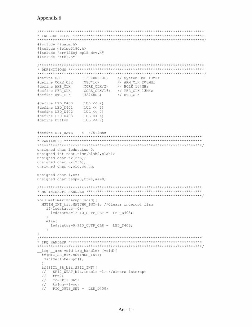
!""#$%&'()(
A6 - 1 -(
/************************************************************************** * INCLUDE FILES *********************************************************** ***************************************************************************/ #include <inarm.h> #include <iolpc3180.h> #include "arm926ej_cp15_drv.h" #include "ttbl.h" /************************************************************************** * DEFINITIONS ************************************************************* ***************************************************************************/ #define OSC (13000000UL) // System OSC 13MHz #define CORE_CLK (OSC*16) // ARM_CLK 208MHz #define AHB_CLK (CORE_CLK/2) // HCLK 104MHz #define PER_CLK (CORE_CLK/16) // PER_CLK 13MHz #define RTC_CLK (32768UL) // RTC_CLK #define LED_D400 (1UL << 2) #define LED_D401 (1UL << 3) #define LED_D402 (1UL << 7) #define LED_D403 (1UL << 6) #define button (1UL << 7) #define SPI_RATE 4 //5.2Mhz /************************************************************************* * VARIABLES ************************************************************** **************************************************************************/ unsigned char ledstatus=0; unsigned int test,time,blah0,blah1; unsigned char tx[256]; unsigned char rx[256]; unsigned char q,old,cc,qq; unsigned char i,zz; unsigned char temp=0,tt=0,aa=0; /************************************************************************* * MS INTERUPT HANDLER **************************************************** **************************************************************************/ void mstimerInterupt(void){ MSTIM_INT_bit.MATCH0_INT=1; //Clears interupt flag if(ledstatus==0){ ledstatus=1;PIO_OUTP_SET = LED_D403; } else{ ledstatus=0;PIO_OUTP_CLR = LED_D403; } } /************************************************************************* * IRQ HANDLER ************************************************************ **************************************************************************/ __irq __arm void irq_handler (void){ if(MIC_SR_bit.MSTIMER_INT){ mstimerInterupt(); } if(SIC1_SR_bit.SPI2_INT){ // SPI2_STAT_bit.intclr =1; //clears interupt // tt=2; // cc=SPI1_DAT; // tx[qq++]=cc; // PIO_OUTP_SET = LED_D400;
!""#$%&'()(
A6 - 2 -(
} } /************************************************************************* * CLOCK INITIALIZATION *************************************************** **************************************************************************/ void ClockInit (void) { // Set Clk dividers HCLKDIV_CTRL_bit.HCLK = 2-1; // 1/2 Pll_clk_out HCLKDIV_CTRL_bit.PERIPH_CLK = 16-1; // 1/16 Pll_clk_out // PLL Init - OSC * 16 = 208MHz HCLKPLL_CTRL_bit.BYPASS = 0; // OSC connected to PLL input HCLKPLL_CTRL_bit.DIRECT = 1; // CCO connected to PLL_Clk output HCLKPLL_CTRL_bit.FEEDBACK = 0; // CC0 connected to N divider input HCLKPLL_CTRL_bit.N = 0; // set divide HCLKPLL_CTRL_bit.M = 16-1; // set multiplier HCLKPLL_CTRL_bit.POWER_DOWN = 1; // Enable Pll // Wait until PLL lock while(!HCLKPLL_CTRL_bit.PLL_LOCK); // Connect Pll_clk_out PWR_CTRL_bit.RUN_MODE = 1; } /************************************************************************* * MSTIMER INITIALIZATION ************************************************* **************************************************************************/ void mstimerInit(void){ MSTIM_CTRL_bit.COUNT_ENAB = 0; // Stop counting MSTIM_CTRL_bit.PAUSE_EN = 0; //runs in debug mode //Match0 MSTIM_MCTRL_bit.MR0_INT = 1; //Enable Interupt Status Generation Match0 MSTIM_MCTRL_bit.RESET_COUNT0 = 1; //Enable Reset of Timer Counter on Match0 MSTIM_MCTRL_bit.STOP_COUNT0 = 0; //Disable Stop Functionality on Match0 MSTIM_CTRL_bit.RESET_COUNT = 1; // Reset the counter while(MSTIM_COUNTER); MSTIM_CTRL_bit.RESET_COUNT = 0; // release reset of the counter MSTIM_MATCH0 = 32768; //Match Value for Match0 MIC_ER_bit.MSTIMER_INT = 1; // Enable Milisecond timer interrupts } /************************************************************************* * SPI1 INITIALIZATION **************************************************** **************************************************************************/ void SPI1Init(void){ //------- TX START_ER_PIN_bit.SPI1_DATIN = 1; //Power up Pin //Set SPI Control Register SPI_CTRL_bit.SPI1_CLK_ENA = 1; SPI_CTRL_bit.SPI1_PIN_SEL = 1; SPI_CTRL_bit.SPI1_CLK_OUT = 1; SPI_CTRL_bit.SPI1_DATIO = 1; SPI1_GLOBAL = 0; // disable SPI1 SPI1_FRM = 1; //1 Frame per transmission //SPI Control Register SPI1_CON = 0; // reset SPI1_CON register SPI1_CON_bit.unidir = 1; // Unidirectional Pins

!""#$%&'()(
A6 - 3 -(
SPI1_CON_bit.thr = 0; // FIFO treshold disabled SPI1_CON_bit.bitnum = 7; // 8its to be tx or rx SPI1_CON_bit.rxtx = 1; // tx SPI1_CON_bit.shift_off = 0; // enable clock generation SPI1_CON_bit.ms = 1; // SPI operating as a master SPI1_CON_bit.mode = 0; SPI1_CON_bit.rate = SPI_RATE; // SPI transfer rate //SPI Interupt Enable Register SPI1_GLOBAL_bit.enable = 1; // Enable SPI2 while (!(SPI1_GLOBAL_bit.enable)); // SPI1_DAT=0; //dummy read } /************************************************************************* * SPI2 INITIALIZATION **************************************************** **************************************************************************/ void SPI2Init(void){ //------- RX START_ER_PIN_bit.SPI2_DATIN = 1; //Power up Pin //Set SPI Control Register SPI_CTRL_bit.SPI2_CLK_ENA = 1; SPI_CTRL_bit.SPI2_PIN_SEL = 1; SPI_CTRL_bit.SPI2_CLK_OUT = 1; SPI_CTRL_bit.SPI2_DATIO = 1; SPI2_GLOBAL = 0; // disable SPI2 SPI2_FRM = 1; //1 Frame per transmission //SPI Control Register SPI2_CON = 0; // reset SPI1_CON register SPI2_CON_bit.unidir = 1; // Unidirectional Pins SPI2_CON_bit.thr = 0; // FIFO treshold disabled SPI2_CON_bit.bitnum = 7; // 8its to be tx or rx SPI2_CON_bit.rxtx = 0; // rx SPI2_CON_bit.shift_off = 0; // disable clock generation SPI2_CON_bit.ms = 1; // SPI operating as a master SPI2_CON_bit.mode = 0; SPI2_CON_bit.rate = SPI_RATE; // SPI transfer rate SPI2_GLOBAL_bit.enable = 1; // Enable SPI2 while (!(SPI2_GLOBAL_bit.enable)); } /************************************************************************* * DMA INITIALIZATION ***************************************************** **************************************************************************/ void DMAInit(void){ DMACLK_CTRL_bit.DMA_CLK_ENA = 1; //All Clocks to DMA enabled
!""#$%&'()(
A6 - 4 -(
//Clear Channel Error Interrupts DMACIntErrClr_bit.DMA_CH0 = 1; DMACIntErrClr_bit.DMA_CH1 = 1; DMACIntTCClear_bit.DMA_CH0 = 1; DMACIntTCClear_bit.DMA_CH1 = 1; //Source and Destination Registers DMACC0SrcAddr = (long)&tx[0]; DMACC0DestAddr = (volatile)&SPI1_DAT; DMACC1SrcAddr = (volatile)&SPI2_DAT; DMACC1DestAddr = (long)&rx[0]; //Disable Linked List Item DMACC0LLI = 0; DMACC1LLI = 0; //DMA Ch0 Control Register DMACC0Control_bit.I = 1; //Terminal Count Interupt disabled DMACC0Control_bit.Prot3 = 1; //Access Cacheable DMACC0Control_bit.Prot2 = 1; //Access Bufferable DMACC0Control_bit.Prot1 = 1; //Access Privileged Mode DMACC0Control_bit.DI = 0; //Destination Address not incremented DMACC0Control_bit.SI = 1; //Source Address incremented DMACC0Control_bit.D = 0; //AHB Master 0 for destination tfr DMACC0Control_bit.S = 0; //AHB Master 0 for source tfr DMACC0Control_bit.DWidth = 0; //8bits DMACC0Control_bit.SWidth = 0; //8bits DMACC0Control_bit.DBSize = 0; //Burst Size 1 DMACC0Control_bit.SBSize = 0; //Burst Size 1 DMACC0Control_bit.TransferSize = 16; //TransferSize //DMA Ch1 Control Register DMACC1Control_bit.I = 0; //Terminal Count Interupt disabled DMACC1Control_bit.Prot3 = 1; //Access Cacheable DMACC1Control_bit.Prot2 = 1; //Access Bufferable DMACC1Control_bit.Prot1 = 1; //Access Privileged Mode DMACC1Control_bit.DI = 1; //Destination Address incremented DMACC1Control_bit.SI = 0; //Source Address not incremented DMACC1Control_bit.D = 0; //AHB Master 0 for destination tfr DMACC1Control_bit.S = 0; //AHB Master 0 for source tfr DMACC1Control_bit.DWidth = 0; //8bits DMACC1Control_bit.SWidth = 0; //8bits DMACC1Control_bit.DBSize = 0; //Burst Size 1 DMACC1Control_bit.SBSize = 0; //Burst Size 1 DMACC1Control_bit.TransferSize = 2; //TransferSize //DMA Ch0 Configuration Register DMACC0Config_bit.H = 0; //Enable DMA requests DMACC0Config_bit.ITC = 0; //Disable Terminal Count Int. DMACC0Config_bit.IE = 0; //Disable Error Int. DMACC0Config_bit.FlowCntrl = 1; //Memory to Peripheral DMACC0Config_bit.DestPeripheral= 11; //Destination Peropheral DMACC0Config_bit.SrcPeripheral = 1; //Source Peripheral DMACC0Config_bit.E = 1; //Enable Ch0 //DMA Ch1 Configuration Register DMACC1Config_bit.H = 0; //Enable DMA requests DMACC1Config_bit.ITC = 0; //Disable Terminal Count Int. DMACC1Config_bit.IE = 0; //Disable Error Int. DMACC1Config_bit.FlowCntrl = 2; //Peripheral to Memory DMACC1Config_bit.DestPeripheral= 1; //Destination Peropheral DMACC1Config_bit.SrcPeripheral = 3; //Source Peripheral

!""#$%&'()(
A6 - 5 -(
DMACC1Config_bit.E = 1; //Enable Ch1 DMACConfig_bit.E = 1; //DMA Controller Enable } /************************************************************************* * INITIALIZATION ROUTINE ************************************************* **************************************************************************/ void initialize(void){ unsigned char *ptrtx = &tx[0]; unsigned char *ptrrx = &rx[0]; char i=0; for(i=0;i<128;i++){ *ptrtx++ = 'A'+i; *ptrrx++ = 0; } // Disable all interrupts MIC_ER = 0; SIC1_ER = 0; SIC2_ER = 0; PIO_OUTP_CLR = LED_D400 | LED_D401 | LED_D402 | LED_D403; TIMCLK_CTRL_bit.WDT_CLK_ENA = 0; // disable watchdog ClockInit(); SPI1Init(); SPI2Init(); // DMAInit(); // PIO_OUTP_SET = LED_D400 | LED_D401 | LED_D402 | LED_D403; } /************************************************************************* * MAIN LOOP ************************************************************** **************************************************************************/ void main(void) { initialize(); __enable_interrupt(); PIO_OUTP_SET = (1UL<<12); a=0; zz=0; while(1) { //for (blah0=0;blah0<200;blah0++); /*Code for DMA Sending on SPI1 as Master********************************/ //************************************************************************ PIO_OUTP_CLR_bit.GPO_12 = 1; while(PIO_OUTP_STATE_bit.GPO_12 == 1); for (blah0=0;blah0<10;blah0++); DMAInit(); for (blah0=0;blah0<50;blah0++); PIO_OUTP_SET_bit.GPO_12 = 1;
!""#$%&'()(
A6 - 6 -(
while(PIO_OUTP_STATE_bit.GPO_12 == 0); //***********************************************************************/ /*Code for DMA Receving on SPI2 as Master********************************/ /*********************************************************************** PIO_OUTP_CLR_bit.GPO_12 = 1; while(PIO_OUTP_STATE_bit.GPO_12 == 1); DMAInit(); SPI2_DAT=0; zz+=2; for (blah0=0;blah0<10;blah0++); PIO_OUTP_SET_bit.GPO_12 = 1; while(PIO_OUTP_STATE_bit.GPO_12 == 0); //***********************************************************************/ /*Code for Polling Receiving on SPI2 as Master*************************/ /************************************************************************ PIO_OUTP_CLR_bit.GPO_12 = 1; while(PIO_OUTP_STATE_bit.GPO_12 == 1); // for (blah0=0;blah0<5;blah0++); if(SPI2_STAT_bit.be == 0){ //while FIFO not empty b=SPI2_DAT; rx[a++]=b; }else{ b=SPI2_DAT; } for (blah0=0;blah0<10;blah0++); PIO_OUTP_SET_bit.GPO_12 = 1; while(PIO_OUTP_STATE_bit.GPO_12 == 0); // for (blah0=0;blah0<5;blah0++); //***********************************************************************/ }; } // main(void)
!""#$%&'()(
A7 - 1 -(
/************************************************************************** * INCLUDE FILES *********************************************************** ***************************************************************************/ #include "inarm.h" #include "iolpc2368.h" /************************************************************************* * Variables ************************************************************** **************************************************************************/ //unsigned char rx[40],tx[40]; unsigned char test,i,a,b,Dummy; #define DMA_SRC 0x7FD00000 #define DMA_DST 0x7FD01000 char *rx ,*tx, *dest_addr, *src_addr; /************************************************************************* * Feed Sequence*********************************************************** **************************************************************************/ void feedseq(void){ PLLFEED = 0xaa; PLLFEED = 0x55; } /************************************************************************* * Initialize Clock******************************************************** **************************************************************************/ void Init_clock(void){ if(PLLSTAT_bit.PLLE){ //If PLL is enabled PLLCON_bit.PLLC = 0; //Disconnect PLL feedseq(); } PLLCON_bit.PLLE = 0; // Disables PLL feedseq(); SCS_bit.OSCEN = 1; // Enable main OSC while(SCS_bit.OSCSTAT == 0); // Wait until main OSC is usable CLKSRCSEL_bit.CLKSRC = 1; // Main Oscillator Selected PLLCFG_bit.MSEL = 11; // Mvalue = 11 +1 PLLCFG_bit.NSEL = 0; // Nvalue = 0 +1 feedseq(); PLLCON_bit.PLLE = 1; // Enables PLL feedseq(); CCLKCFG = 3; // CCLKSEL = 3 +1 while(PLLSTAT_bit.PLOCK==0); // Wait for PLOCK to be asserted //check to ensure M and N values are correct while ((PLLSTAT_bit.MSEL !=11 ) && (PLLSTAT_bit.NSEL != 0) ); PLLCON_bit.PLLC = 1; // Connects PLL feedseq(); } /************************************************************************* * Initialize SSP0 ******************************************************** **************************************************************************/ void Init_SSP0(void){ //Transmit TX
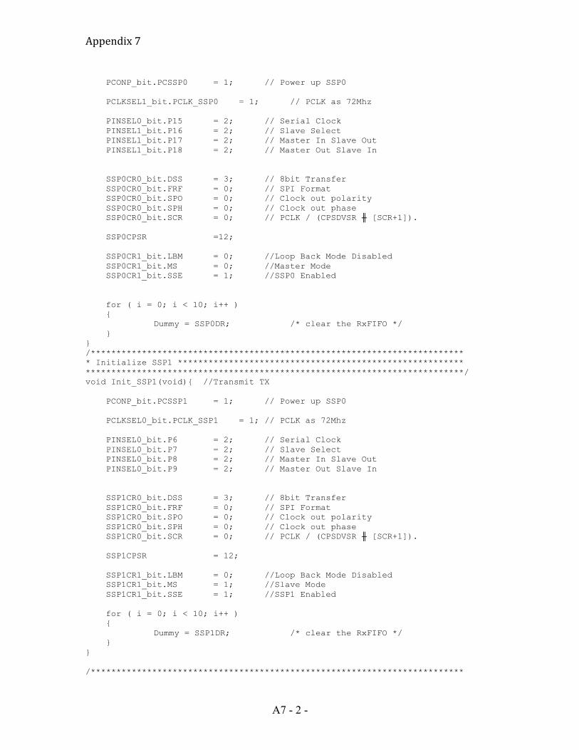
!""#$%&'()(
A7 - 2 -(
PCONP_bit.PCSSP0 = 1; // Power up SSP0 PCLKSEL1_bit.PCLK_SSP0 = 1; // PCLK as 72Mhz PINSEL0_bit.P15 = 2; // Serial Clock PINSEL1_bit.P16 = 2; // Slave Select PINSEL1_bit.P17 = 2; // Master In Slave Out PINSEL1_bit.P18 = 2; // Master Out Slave In SSP0CR0_bit.DSS = 3; // 8bit Transfer SSP0CR0_bit.FRF = 0; // SPI Format SSP0CR0_bit.SPO = 0; // Clock out polarity SSP0CR0_bit.SPH = 0; // Clock out phase SSP0CR0_bit.SCR = 0; // PCLK / (CPSDVSR ! [SCR+1]). SSP0CPSR =12; SSP0CR1_bit.LBM = 0; //Loop Back Mode Disabled SSP0CR1_bit.MS = 0; //Master Mode SSP0CR1_bit.SSE = 1; //SSP0 Enabled for ( i = 0; i < 10; i++ ) { Dummy = SSP0DR; /* clear the RxFIFO */ } } /************************************************************************* * Initialize SSP1 ******************************************************** **************************************************************************/ void Init_SSP1(void){ //Transmit TX PCONP_bit.PCSSP1 = 1; // Power up SSP0 PCLKSEL0_bit.PCLK_SSP1 = 1; // PCLK as 72Mhz PINSEL0_bit.P6 = 2; // Serial Clock PINSEL0_bit.P7 = 2; // Slave Select PINSEL0_bit.P8 = 2; // Master In Slave Out PINSEL0_bit.P9 = 2; // Master Out Slave In SSP1CR0_bit.DSS = 3; // 8bit Transfer SSP1CR0_bit.FRF = 0; // SPI Format SSP1CR0_bit.SPO = 0; // Clock out polarity SSP1CR0_bit.SPH = 0; // Clock out phase SSP1CR0_bit.SCR = 0; // PCLK / (CPSDVSR ! [SCR+1]). SSP1CPSR = 12; SSP1CR1_bit.LBM = 0; //Loop Back Mode Disabled SSP1CR1_bit.MS = 1; //Slave Mode SSP1CR1_bit.SSE = 1; //SSP1 Enabled for ( i = 0; i < 10; i++ ) { Dummy = SSP1DR; /* clear the RxFIFO */ } } /*************************************************************************
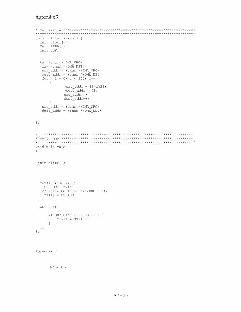
!""#$%&'()(
A7 - 3 -(
* Initialize ************************************************************** **************************************************************************/ void initialize(void){ Init_clock(); Init_SSP0(); Init_SSP1(); tx= (char *)DMA_SRC; rx= (char *)DMA_DST; src_addr = (char *)DMA_SRC; dest_addr = (char *)DMA_DST; for ( i = 0; i < 200; i++ ) { *src_addr = 65+i%26; *dest_addr = 48; src_addr++; dest_addr++; } src_addr = (char *)DMA_SRC; dest_addr = (char *)DMA_DST; }; /************************************************************************* * MAIN LOOP ************************************************************** **************************************************************************/ void main(void) { initialize(); for(i=0;i<26;i++){ SSP0DR= tx[i]; // while(SSP1STAT_bit.RNE ==1); rx[i] = SSP1DR; } while(1){ if(SSP1STAT_bit.RNE == 1){ *rx++ = SSP1DR; } }; }; Appendix 7 A7 - 1 -
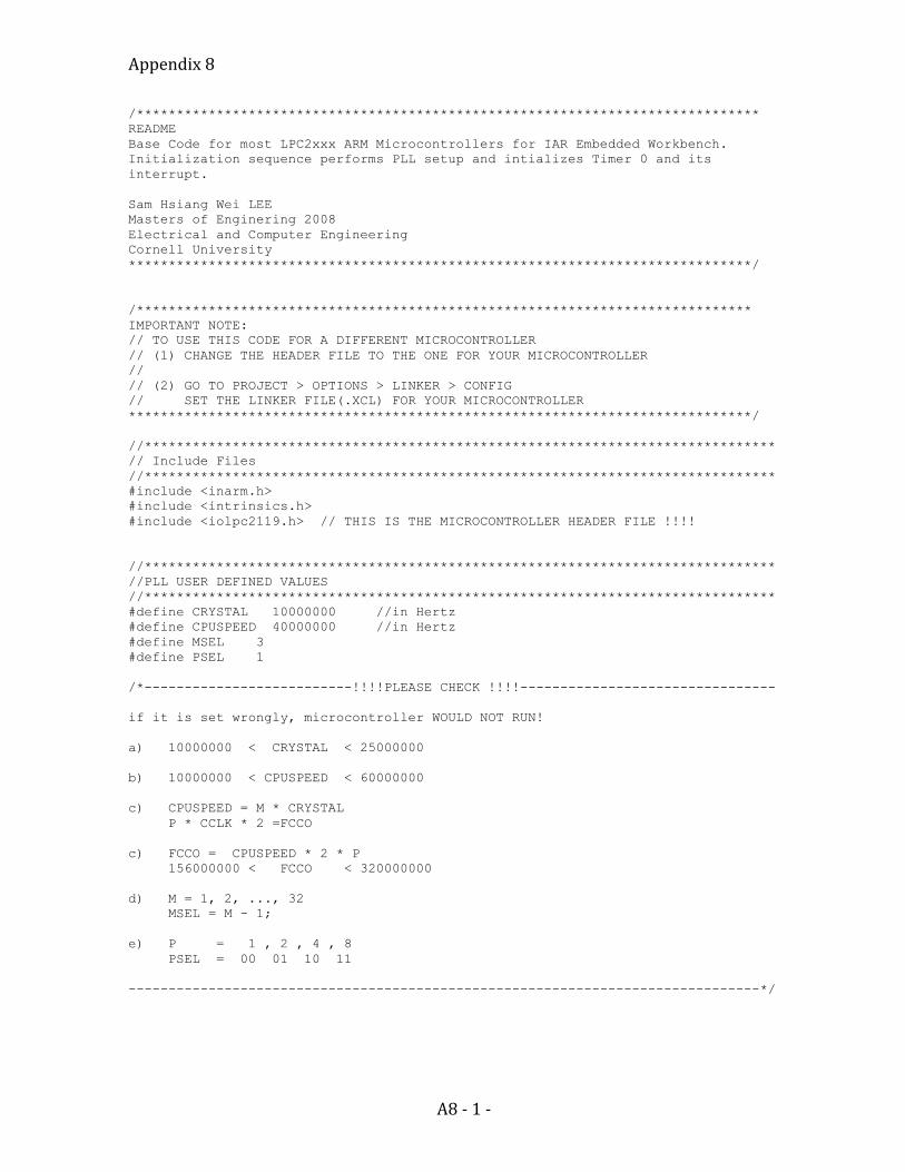
!""#$%&'()(
!)(*(+(*(
/******************************************************************************
README
Base Code for most LPC2xxx ARM Microcontrollers for IAR Embedded Workbench.
Initialization sequence performs PLL setup and intializes Timer 0 and its
interrupt.
Sam Hsiang Wei LEE
Masters of Enginering 2008
Electrical and Computer Engineering
Cornell University
******************************************************************************/
/*****************************************************************************
IMPORTANT NOTE:
// TO USE THIS CODE FOR A DIFFERENT MICROCONTROLLER
// (1) CHANGE THE HEADER FILE TO THE ONE FOR YOUR MICROCONTROLLER
//
// (2) GO TO PROJECT > OPTIONS > LINKER > CONFIG
// SET THE LINKER FILE(.XCL) FOR YOUR MICROCONTROLLER
******************************************************************************/
//*******************************************************************************
// Include Files
//*******************************************************************************
#include <inarm.h>
#include <intrinsics.h>
#include <iolpc2119.h> // THIS IS THE MICROCONTROLLER HEADER FILE !!!!
//*******************************************************************************
//PLL USER DEFINED VALUES
//*******************************************************************************
#define CRYSTAL 10000000 //in Hertz
#define CPUSPEED 40000000 //in Hertz
#define MSEL 3
#define PSEL 1
/*--------------------------!!!!PLEASE CHECK !!!!--------------------------------
if it is set wrongly, microcontroller WOULD NOT RUN!
a) 10000000 < CRYSTAL < 25000000
b) 10000000 < CPUSPEED < 60000000
c) CPUSPEED = M * CRYSTAL
P * CCLK * 2 =FCCO
c) FCCO = CPUSPEED * 2 * P
156000000 < FCCO < 320000000
d) M = 1, 2, ..., 32
MSEL = M - 1;
e) P = 1 , 2 , 4 , 8
PSEL = 00 01 10 11
-------------------------------------------------------------------------------*/
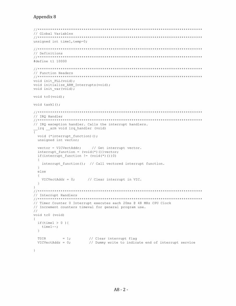
!""#$%&'()(
!)(*(+(*(
//******************************************************************************* // Global Variables //******************************************************************************* unsigned int time1,temp=0; //******************************************************************************* // Definitions //******************************************************************************* #define t1 10000 //******************************************************************************* // Function Headers //******************************************************************************* void init_PLL(void); void initialize_ARM_Interrupts(void); void init_var(void); void tc0(void); void task1(); //******************************************************************************* // IRQ Handler //******************************************************************************* // IRQ exception handler. Calls the interrupt handlers. __irq __arm void irq_handler (void) { void (*interrupt_function)(); unsigned int vector; vector = VICVectAddr; // Get interrupt vector. interrupt_function = (void(*)())vector; if(interrupt_function != (void(*)())0) { interrupt_function(); // Call vectored interrupt function. } else { VICVectAddr = 0; // Clear interrupt in VIC. } } //******************************************************************************* // Interrupt Handlers //******************************************************************************* // Timer Counter 0 Interrupt executes each 20ms @ 48 MHz CPU Clock // Increment counters timeval for general program use. // void tc0 (void) { if(time1 > 0 ){ time1--; } T0IR = 1; // Clear interrupt flag VICVectAddr = 0; // Dummy write to indicate end of interrupt service }
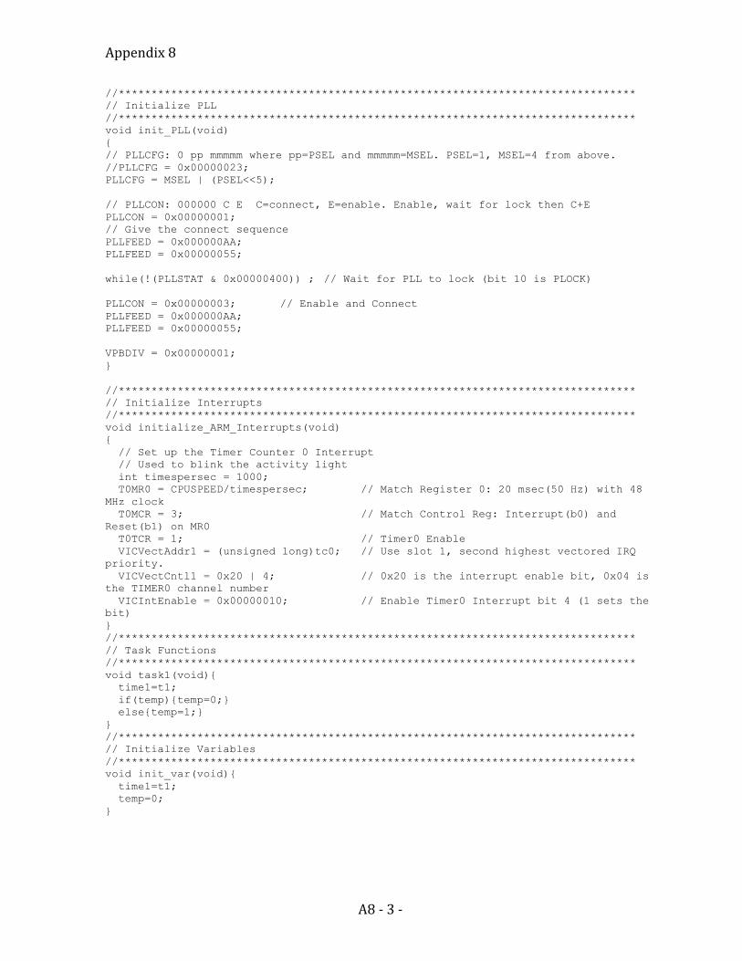
!""#$%&'()(
!)(*(+(*(
//******************************************************************************* // Initialize PLL //******************************************************************************* void init_PLL(void) { // PLLCFG: 0 pp mmmmm where pp=PSEL and mmmmm=MSEL. PSEL=1, MSEL=4 from above. //PLLCFG = 0x00000023; PLLCFG = MSEL | (PSEL<<5); // PLLCON: 000000 C E C=connect, E=enable. Enable, wait for lock then C+E PLLCON = 0x00000001; // Give the connect sequence PLLFEED = 0x000000AA; PLLFEED = 0x00000055; while(!(PLLSTAT & 0x00000400)) ; // Wait for PLL to lock (bit 10 is PLOCK) PLLCON = 0x00000003; // Enable and Connect PLLFEED = 0x000000AA; PLLFEED = 0x00000055; VPBDIV = 0x00000001; } //******************************************************************************* // Initialize Interrupts //******************************************************************************* void initialize_ARM_Interrupts(void) { // Set up the Timer Counter 0 Interrupt // Used to blink the activity light int timespersec = 1000; T0MR0 = CPUSPEED/timespersec; // Match Register 0: 20 msec(50 Hz) with 48 MHz clock T0MCR = 3; // Match Control Reg: Interrupt(b0) and Reset(b1) on MR0 T0TCR = 1; // Timer0 Enable VICVectAddr1 = (unsigned long)tc0; // Use slot 1, second highest vectored IRQ priority. VICVectCntl1 = 0x20 | 4; // 0x20 is the interrupt enable bit, 0x04 is the TIMER0 channel number VICIntEnable = 0x00000010; // Enable Timer0 Interrupt bit 4 (1 sets the bit) } //******************************************************************************* // Task Functions //******************************************************************************* void task1(void){ time1=t1; if(temp){temp=0;} else{temp=1;} } //******************************************************************************* // Initialize Variables //******************************************************************************* void init_var(void){ time1=t1; temp=0; }
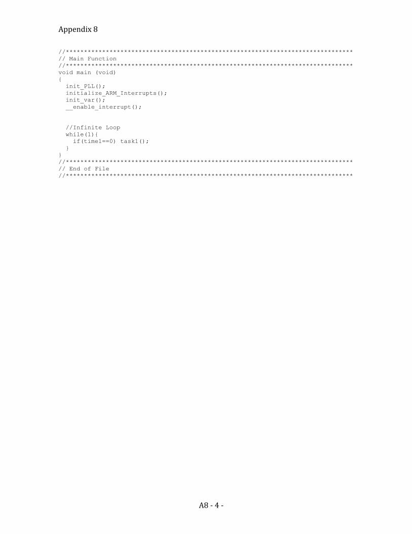
!""#$%&'()(
!)(*(+(*(
//******************************************************************************* // Main Function //******************************************************************************* void main (void) { init_PLL(); initialize_ARM_Interrupts(); init_var(); __enable_interrupt(); //Infinite Loop while(1){ if(time1==0) task1(); } } //******************************************************************************* // End of File //*******************************************************************************
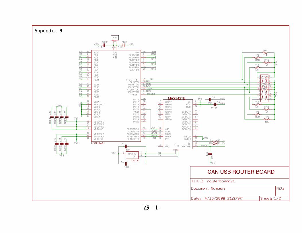
CAN USB ROUTER BOARD
MAX3421E
CSTCE
LPC2194/01
GPIN71
VL2
GND_03
GPOUT04
GPOUT15
GPOUT26
GPOUT37
GPOUT48
GPOUT59
GPOUT610
GPOUT711
~RES12
SCLK13
~SS14
MISO15
MOSI16
GPX17
INT18
GND_119
D-20
D+21
VBCOMP22
VCC23
XI
24
XO
25
GPIN026
GPIN127
GPIN228
GPIN329
GPIN430
GPIN531
GPIN632
X01
GND2
X13
C1
C2
C3
R1R2
C5
C4
P0.21/RD31
P0.22/TD32
P0.23/RD23
P1.194
P0.24/TD25
VSS_06
VDDA3V37
P1.188
P0.25/RD19
TD110
P0.2711
P1.1712
P0.2813
P0.2914
P0.3015
P1.1616
VDD1V8_017
VSS_118
P0.019
P1.31/~TRST20
P0.121
P0.222
VDD3V3_023
P1.26/RTCK24
VSS_225
P0.326
P0.427
P1.2528
P0.529
P0.630
P0.731
P1.2432
P0.833
P0.934
P0.1035
P1.2336
P0.1137
P0.12/RD438
P0.13/TD439
P1.2240
P0.1441
VSS_342
VDD3V3_143
P1.2144
P0.1545
P0.16/EINT046
P0.17/SCK147
P1.2048
VDD1V8_149
VSS_450
VDD3V3_251
P1.30/TMS52
P0.18/MISO153
P0.19/MOSI154
P0.20/SSEL155
P1.29/TCK56
~RESET57
VSSA_PLL58
VSSA59
P1.28/TDI60
XT
AL2
61
XT
AL1
62
VDDA1V863
P1.27/TDO64
1 23 45 67 89 10
11 1213 1415 1617 1819 20
JT
AG
1
GND
GND
GND
GND
GND
GND
GND
GND
GND
VTARGETVREF
NTRST
TDI
TMS
TCK
RTCK
TDO
RST
OBGRQ
OBGACK
R13
R14
R15
R16
R17
R18
R19
R20
11
33
C11C12C
13
C14
C15
C16
C17
C18
C19 VSS
VSS
VSS
VSS
VSS
VS
S
VSS
VS
S
VSS
VSS
VSS
1V8
3V
3
3V3
3V3
X0X1
SCLK~SS
MISO
D+D-
VBUS
UINT
RD3TD3
TD2RD2
TD1
TD4RD4
TDO
TDI
TCKTMS
RTCK
~TRST
~RESET
RD1
MOSI
1A1B1C2A2B2C3A3B3C4A4B4C
5A5B
6A6B6C
5C
18pF
18pF
0.1uF
3333
1.0
uF
1.0uF
10k
10k
10k
10k
10k
10k
10k10k
38pF38pF
100nF
100nF
100nF
100nF
100nF
100nF
100nF
Robots
Appendix 9
Robots
A9 -1-

CAN USB ROUTER BOARD
LM2937
LTC3419
MAX3050
MAX3050
MAX3050
MAX3050
TRI-COLOR LED
TRI-COLOR LED
TRI-COLOR LED
TRI-COLOR LED
TRI-COLOR LED
TRI-COLOR LED
INPUT1
OUTPUT3
GND02
GND14
VFB11
RUN12
MODE3
SW14
GND05
GND16
VIN7
SW28
RUN29
VFB210
C6
C7
L1
R3
R4
C8 C9
L2
R5
R6
C10
LED1 R12
TXD1
GND2
VCC3
RXD4
~SHDN5
CANL6
CANH7
RS8
TXD1
GND2
VCC3
RXD4
~SHDN5
CANL6
CANH7
RS8
TXD1
GND2
VCC3
RXD4
~SHDN5
CANL6
CANH7
RS8
TXD1
GND2
VCC3
RXD4
~SHDN5
CANL6
CANH7
RS8
C20
C21
C22
C23
C24
C25
C26
C27
C28
C29
C30
C31
C32
C33
C34
C35
R7
+1
R2
G3
B4
R8R9
R10
+1
R2
G3
B4
R11R21
R22
+1
R2
G3
B4
R23R24
R25
+1
R2
G3
B4
R26R27
R28
+1
R2
G3
B4
R29R30
R31
+1
R2
G3
B4
R32R33
VSSVSS
VS
S
VSS
VSS
VSSVSS
VSS
VSS
VSS
VSS
VSS
VSS
VS
SV
SS
VS
SV
SS
1V8 3V3
3V3
3V3
3V3
3V3
3V3
3V3
3V3
VIN
VIN
5V
5V
5V
5V
5V
SW1VFB1 VFB2
SW2
TD1
RD1
TD2
RD2
TD3
RD3
TD4
RD4
1A1B1C
2A2B2C
3A3B3C
4A4B4C
5A5B5C
6A6B6C
10uF
22pF
3.3uH
118k
59k
10uF 22pF
3.3uH
267k
59k
10uF
300
30pF
30pF
30pF
30pF
100nF
100nF
100nF
100nF
100pF
100pF
100pF
100pF
100pF
100pF
100pF
100pF
300300300
300300300
300300300
300300300
300300300
300300300
Robots
Appendix 9
Robots
A9 -2-