Design of a Multi-Channel Integrated Circuit Particle...
98
Design of a Multi-Channel Integrated Circuit for Use in Nuclear Physics Experiments Where Particle Identification is Required by Justin M. Proctor, Bachelor of Science A Thesis Submitted in Partial Fulfillment of the Requirements for the Master of Science Degree Department of Electrical and Computer Engineering in the Graduate School Southern Illinois University Edwardsville Edwardsville, Illinois December 13, 2007
Transcript of Design of a Multi-Channel Integrated Circuit Particle...

Design of a Multi-Channel Integrated Circuit
for Use in Nuclear Physics Experiments Where
Particle Identification is Required
by Justin M. Proctor, Bachelor of Science
A Thesis Submitted in Partial Fulfillment of the Requirements for the Master of Science Degree
Department of Electrical and Computer Engineering in the Graduate School
Southern Illinois University Edwardsville Edwardsville, Illinois
December 13, 2007

ABSTRACT
DESIGN OF A MULTI-CHANNEL INTEGRATED CIRCUIT
FOR USE IN NUCLEAR PHYSICS EXPERIMENTS WHERE
PARTICLE IDENTIFICATION IS REQUIRED
by
Justin Proctor
Advisor: Dr. George L Engel
The thesis presents the design, simulation, and layout of an eight channel
integrated circuit (IC) for use in nuclear physics experiments where particle
identification, total pulse height, and relative timing information is needed. The
design employs a technique known as pulse shape discrimination (PSD) to classify
the incident radiation. Each of the eight channels is composed of a time-to-voltage
converter (TVC) with two time ranges (0.5 μsec, 2 μsec) and three sub-channels.
Each of the sub-channels consists of a gated integrator with 8 programmable
charging rates and an externally programmable gate generator that defines the
start (with 4 time ranges) and width (with 4 time ranges) of the gate relative to an
external discriminator signal. The chip supports 3 triggering modes.
The IC produces four sparsified analog pulse trains (3 integrator outputs
and 1 TVC output) with synchronized addresses for off-chip digitization with a
pipelined ADC. The micro-chip, christened PSD8C, with two bias modes occupies
an area of approximately 2.8 mm x 5.7 mm and has an estimated power
dissipation of 135 mW in the high-bias mode. The chip is to be fabricated in the
AMIS 0.5-micron NWELL process (C5N) in early 2008. This work was initiated by
the heavy-ion nuclear chemistry and physics group at Washington University in
Saint Louis and is funded by NSF Grant #06118996.
ii

ACKNOWLEDGEMENTS
I would like to thank Dr. George Engel for his support and guidance as well
as the opportunity to participate in this research project. The advice and support
of Dr. Brad Noble in making the computer systems run smoothly was critical to our
research and much appreciated. I would also like to thank Dr. Scott Smith and
Dr. Robert LeAnder. They gave me the opportunity to complete course
requirements in such a way as to gain a deeper understanding of this project.
I would like to thank Dr. Lee Sobotka, Mr. Jon Elson, and Dr. Robert
Charity, Department of Chemistry, Washington University Saint Louis, who funded
the initial research. Their help was also instrumental in understanding the
purpose and requirements of the project.
I would also like to thank Michael Hall and other research assistants,
present and past, whose work has been instrumental in laying the ground work
and developing the PSD8C. Graduate assistants Dinesh Dasari and Nagendra
Valluru were responsible for the physical layout of the PSD8C IC. Without their
efforts, the completion of PSD8C would not have been possible. I have learned
much in my interactions with these fellow graduate students.
Finally, I wish to thank my family for being patient with me and encouraging
me throughout the entire of my college experience. In particular, I would like to
thank my wife Emelia Proctor, without whom I may not have finished.
iii

TABLE OF CONTENTS ABSTRACT ........................................................................................................... ii ACKNOWLEDGEMENTS ..................................................................................... iii LIST OF FIGURES ................................................................................................vi LIST OF TABLES ................................................................................................viii Chapter
1. INTRODUCTION .....................................................................................1
Background……………………………………………………………………….. 1 Need For Integrated Circuit……………………………………………………. 2 First Experiment to Use Integrated Circuit………………………………… 2 Previous Work…………………………………………………………………….. 5 Object and Scope of Thesis……………………………………………………..9
2. PSD8C ARCHITECTURE ..................................................................... 10
Overview of Chip .……………………………………………………………… 10 PSD8C Features………………………………………………………………… 11 Common Channel……………………………………………………………….12 Signal Processing Channel…………………………………………………… 13 Signal Processing Sub-Channel…………………………………………….. 17 Proof of Concept………………………………………………………………… 20
3. PSD8C CIRCUIT DESIGN.................................................................... 22
Common Channel .......................................................................... 22
Biasing circuits.................................................................... 23 Bandgap voltage reference ......................................... 23 Current sources......................................................... 24 Temperature-independent current sources................. 25
Readout electronics.............................................................. 27 Output buffers..................................................................... 27
Core amplifier ............................................................ 28 Single-ended-to-differential converter......................... 28
Channel ......................................................................................... 29 Time-to-voltage converter ..................................................... 29 Hit logic ............................................................................... 30 Triggering logic .................................................................... 30
Sub-Channel.................................................................................. 31 Gate generator ..................................................................... 31
Comparator ............................................................... 32 Ramp generator ......................................................... 32
Integrator ............................................................................ 32 Core op amp .............................................................. 32
iv
Resistor array ............................................................ 33 Integrating capacitor.................................................. 34 Offset-canceling DAC ................................................. 34
4. SIMULATED PERFORMANCE OF PSD8C .......................................... 36
Common Channel .......................................................................... 36 Bandgap .............................................................................. 36 Current references ............................................................... 37 Output buffer ..................................................................... 37
Frequency response ................................................... 37 Linearity .................................................................... 39
Signal Processing Channel ............................................................. 40 Integrator linearity ............................................................... 40 TVC linearity........................................................................ 42
Signal Processing Sub-Channel ...................................................... 44 DAC..................................................................................... 45
DAC range ................................................................. 45 DAC temperature dependence.................................... 46
VTC ..................................................................................... 46 VTC range and linearity ............................................. 47 VTC temperature dependence .................................... 51
Integrator op amp ................................................................ 52 Frequency response ................................................... 53 Output voltage swing ................................................. 54 Noise performance ..................................................... 54
Chip .............................................................................................. 54 Configuring chip .................................................................. 54 Acquiring data ..................................................................... 55
Power Dissipation .......................................................................... 56 Area Distribution ........................................................................... 57 Layout of Chip ............................................................................... 58
5. SUMMARY/FUTURE WORK ........................................................... 61
Summary....................................................................................... 61 Conclusions ................................................................................... 62 Future Work .................................................................................. 62
REFERENCES.......................................................................................... 64 APPENDICES
A. VerilogA Code......................................................................... 67 B. PSD8C Pin Descriptions ......................................................... 73 C. PSD8C Bonding Diagram........................................................ 90
v

LIST OF FIGURES
Figure Page
1.1 Proposed experimental setup................................................................. 3
1.2 HINP16C channel.................................................................................. 5
1.3 HINP16C layout .................................................................................... 8
2.1 Overview of analog pulse-shape discrimination integration scheme ...... 10
2.2 Architecture of a single channel........................................................... 14
2.3 Trigger logic ........................................................................................ 15
2.4 Sub-channel architecture.................................................................... 18
2.5 Delay before auto-reset versus control voltage ..................................... 20
2.6 Pulse-shape discrimination plots ......................................................... 21
3.1 PSD8C triggering logic......................................................................... 28
4.1 Frequency response of buffer’s core amplifier....................................... 38
4.2 Buffer linearity for negative outputs .................................................... 39
4.3 Buffer linearity positive outputs .......................................................... 40
4.4 Integrator linearity for low- and high-bias modes ................................. 41
4.5 Integrator linearity as function of process corner ................................. 42
4.6 TVC linearity in 500ns mode ............................................................... 43
4.7 TVC linearity in 2μs mode ................................................................... 44
4.8 DAC range .......................................................................................... 45
4.9 DAC temperature dependence ............................................................. 46
4.10 VTC transfer characteristic (Mode 0).................................................... 48
4.11 VTC transfer characteristic (Mode 1).................................................... 49
4.12 VTC transfer characteristic (Mode 2).................................................... 50
4.13 VTC transfer characteristic (Mode 3).................................................... 51
4.14 VTC temperature dependence (Mode 0)................................................ 52
vi

4.15 Frequency response of the integrating op amp ..................................... 53
4.16 PSD8C in process of acquiring data..................................................... 55
4.17 Breakdown of PSD8C power by circuit function (high-bias mode)......... 56
4.18 Breakdown of PSD8C power by circuit function (low-bias mode) .......... 57
4.19 Breakdown of PSD8C area by circuit function...................................... 58
4.20 Final layout of PSD8C ......................................................................... 59
vii

viii
LIST OF TABLES
Table Page
2.1 Configuration register ............................................................................ 13
2.2 Trigger modes ........................................................................................ 15
2.3 TVC timing ranges ................................................................................. 17
2.4 Resistor values that set charging rate..................................................... 17
2.5 Delay and integration width ranges........................................................ 19
3.1 PSD8C biasing voltages ......................................................................... 25
3.2 PSD8C temperature-independent biasing voltages.................................. 26
3.3 Resistor values ...................................................................................... 33
4.1 VTC conversion factor (Mode 0) .............................................................. 47
4.2 VTC conversion factor (Mode 1) .............................................................. 48
4.3 VTC conversion factor (Mode 2) .............................................................. 49
4.4 VTC conversion factor (Mode 3) .............................................................. 50
4.5 VTC temperature coefficient (Mode 0) ..................................................... 52
CHAPTER 1
INTRODUCTION
Background
This thesis will present the design of a custom integrated circuit (IC) for use
in nuclear physics experiments. The micro-chip will complement an existing
(shaped and peak-sensing) analog chip (HINP16C) designed by the SIUE IC Design
Research Laboratory in 2002. The chip described is capable of pulse-shape
discrimination (PSD). The work over the past 1½ years was made possible by a
generous grant from the National Science Foundation (NSF Grant#06118996).
While a pulse-shape capable CMOS chip has never been made, the
engineering effort required to design such a chip was modest as the high-gain/low
noise amplifier is not incorporated on the proposed chip, and we were able to re-
use many of the circuits that had been developed for the HINP16C chip. The PSD
IC described in this thesis will be suitable for use with both CsI(Tl) (used for
charge-particle discrimination) and liquid scintillator (used for neutron-gamma
discrimination) detectors. Furthermore, the IC can also be used with scintillators
without PSD capability in the wave form. In such cases the multiple integration
logic developed for PSD can be used as a pile-up rejector.
The IC Design Research Laboratory at Southern Illinois University
Edwardsville is part of an interuniversity collaboration with a broad program of
studies in low- and intermediate-energy nuclear physics. The experimental
program of this collaboration requires the use of large arrays of scintillators which
not only provide the pulse-height of the incoming ionizing radiation but can also
distinguish between charged particles, neutrons, and gamma rays.

2
Need For Integrated Circuit
The need for high density analog signal processing in the low- and
intermediate-energy nuclear physics community is widespread [Eng:06]. No
commercial microchip is currently available with the following requested features:
o Capable of particle identification (α particle, γ-ray, etc.)
o Able to support multiple radiation detectors
o Possess multiple (separate) integration regions with independent control
of charging rate in each region which can be used for high-quality pulse
shape discrimination (PSD).
o Built-in high-quality timing circuitry
o Multiple triggering modes
o Analog multiplicity output indicating number of detectors impacted by
radiation
o Able to be used with wide variety of detectors (CsI, photodiodes, liquid
scintillator)
o Able to provide data sparsification
First Experiment to Use Integrated Circuit
The integrated circuit (IC) (with the features listed above) will be suitable for
use in a wide variety of recently planned nuclear physics experiments. We will
describe [Eng:06] one such experiment, directed at the Density dependence of the
Equation of State (EOS) that has already been approved by the Program advisory
Committee (PAC) of the National Superconducting Cyclotron Laboratory (NSCL).
This EOS experiment will be performed in Fall 2008, in the newly configured S2
vault, and will be the first one to use the PSD chip described in this thesis.

3
Our approved experiment (see Figure 1.1) will use the approximately 200
CsI(Tl) scintillator detectors of the MINIBALL [Des:90], the MSU neutron walls
[Zec:97] (100 channels), and another 50 (approximately) discrete neutron detectors
[Sar:04], all of which require PSD analysis. An additional 100 element forward
array also must be instrumented with QDC’s and TDC’s. All of these detector
systems could be serviced by the proposed technology. Beyond this, our recently
completed HiRA array [Wal:07], with over 1000 Si channels, will be used for high
resolution charged-particle detection. Our HINP16C micro-chip will service these Si
channels [Eng:07].
HiRA
100
200 Multiplicity
(300)
Figure 1.1: Proposed experimental setup

4
The CsI(Tl) detectors at backward angles (see Figure 1.1) are used to
determine the reaction plane. The flow for neutrons and charged particles from the
reaction is extracted from the large n (Wall) detectors and the HiRA, respectively.
The forward array of fast scintillators provides a high quality event time (triggered
by protons), needed for the start time for the n time of flight (ToF). We will not
discuss the details of the forward array in this thesis. Despite the fact that such
detectors do not contain significant PSD information, we intend (for convenience) to
process the signals from this array using the IC described in this thesis.
The approved experiment could be done with conventional (off-the-shelf)
electronics, i.e., individually gated CAEN QDC’s. The “off the shelf” digitizer cost
would be in excess of $100,000 (in excess of $150,000 if one counts the crates and
interconnections.) On the other hand, by designing a custom IC to do PSD, we are
creating a new and flexible technology (at a roughly similar one-time cost), that can
be used by us or by others who need many channels of PSD, with a very modest
expenditure. This might allow programs to proceed which could not, under the
present budget climate, and to do so with dedicated electronics.
Moreover, we can envision uses for the IC beyond basic science laboratory
experiments. While circuits capable of particle identification are available in
discrete analog form (bulky!) and in digital form (power-hungry!), none are available
in a low-power, small, integrated form. As a result, mass production of PSD
technology (at a reasonable cost) is currently unavailable, but is actively being
sought by our government’s Department of Homeland Security. Our research has
the potential to greatly reduced false positives from detectors sensitive to different
types of radiation. Thus, our IC may someday play an important role in the
detection of nuclear attacks launched by terrorists against our nation!

5
Previous Work
The current goal of this research is to produce a micro-chip that will
complement our existing (shaped and peak-sensing) analog chip (called HINP16C)
with one capable of particle identification using pulse-shape discrimination (PSD).
A brief description of HINP16 is provided below [Eng:07]. A basic understanding of
the operation of HINP16C is helpful when trying to understand the work presented
in this thesis. Many sub-circuits used in HINP16C were re-used in the PSD chip
described in later chapters of this thesis. Also, by presenting an overview of
HINP16C we hope the reader will see how the new PSD IC complements the
existing chip.
A block diagram for the HINP16C chip is shown in Figure 1.2. The IC was
fabricated in the AMIS 0.5 μm n-well process (C5N) available through MOSIS (MOS
Implementation Services). This non-silicided CMOS process has 3 metal layers and
supports double poly capacitors (1 fF / μm2). It also provides to the designer a high
resistance (1 kΩ per square) poly layer.
Figure 1.2: HINP16C channel
6
Each of the 16 channels of the HINP16C consists of a charge sensitive
amplifier (CSA) with two gain modes: high-gain (15 mV/MeV or 0.4 mV/ fC) and
low-gain (3 mV/MeV or 0.08 mV / fC). The high-gain mode is linear up to
approximately 100 MeV while the low-gain mode is linear up to approximately 500
MeV. The CSA output is split to feed energy and timing branches, each of which
produce sparsified pulse trains with synchronized addresses for off-chip
digitization with a pipelined ADC.
The energy leg consists of a shaping filter with a fast return to baseline, <
20 μs. This slow-shaper is followed by a continuous-time peak sampling circuit.
Simulated and measured (using a pulser) energy resolution is 38 keV with an ideal
75 pF load in the high-gain (100 MeV) mode.
The timing leg consists of a Nowlin pseudo constant-fraction discriminator
(CFD) composed of a leading-edge and a zero-crossing discriminator. The zero-
crossing discriminator has its offsets dynamically nulled. A 6-bit DAC is used to
correct offsets associated with the leading-edge circuit as well as to set CFD
threshold levels.
When the CFD fires it starts a time-to-voltage converter (TVC). The TVC
circuit has two (selectable) measurement ranges: 250 ns and 1 μs. The charging
concludes with a common stop signal applied to all channels. The TVC circuit and
the peak sampling circuit are automatically reset after a user-controlled variable
delay time, referenced to when the CFD fires. To acquire the analog information,
the user must supply a pulse to veto the reset. This veto thus selects an event for
readout and digitization.
A fast logical ‘OR’ signal and an analog output proportional to the number of
channels that were hit, ‘MULT’, are available for off-chip high-level logical decisions

7
and to decide, for example, if the veto reset is to be sent. The logical ‘OR’ and
‘MULT’ are also automatically reset unless vetoed by the user.
A central common channel provides biasing for the 16 processing channels
and contains the readout electronics. A 48-bit configuration register allows the
user to select: CSA gain/input option, processing for either positive or negative
CSA pulses, TVC measurement range, a test mode (allowing CSA, Shaper and CFD
inspection of any channel) , to selectively disable CFD outputs on a channel-by-
channel basis, and to assign an 8-bit ID to the chip. The chip only responds when
an externally applied chip address matches the ID stored in the chip's
configuration register.
In October, 2008 a revised version of HINP16C was submitted for
fabrication. The “revised” HINP16C is expected to have performance superior to
that of the existing chip. The layout of the revised HINP16C chip is presented in
Figure 1.3. The biasing and circuits used for configuring the IC as well as for
readout are located in the center (“common” channel) of the chip. Eight channels
lie to the left of this “common” area, and eight channels lie to the right.
To date the HINP16C chip has been used in eight experiments. The
flexibility of this chip (the fact that it is not so ``application” specific) allows other Si
devices to be used and therefore experiments with intermediate channel counts
can benefit from the cost savings of chip analog processing coupled with modern
pipeline ADCs. HINP16C was capable of servicing sixteen 32 x 32 strip double-
sided Si 1.5 mm “E” detectors and sixteen 65 μm, 32 strip single-sided Si “dE”
detectors of HiRA [Wal:07]. These experiments made use of both the internal (for
the “E”’s) and external CSA’s (for the “dE”’s) and were run in both sparsified and all
channel dump modes.
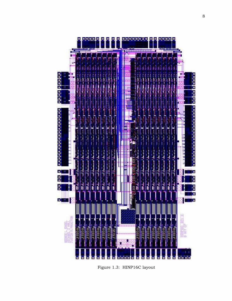
8
Figure 1.3: HINP16C layout

9
Object and Scope of Thesis
The object of this thesis work was to design an integrated circuit, which has
been christened PSD8C (Pulse Shape Discrimination – 8 Channels) that can be
used to classify the type of radiation striking the detectors by using a technique
known as “pulse shape discrimination” i.e. PSD. A detailed discussion of the PSD
technique can be found in a companion thesis [Hall:07] by another graduate
student (Michael J. Hall) working on the design of PSD8C.
This thesis consists of five chapters. A list of features and the architecture
of the PSD8C chip is described in Chapter 2. Chapter 3 describes the electronic
circuit design of the various sub-circuits that comprise PSD8C. Chapter 4
contains the simulation results and demonstrates that PSD8C functions correctly.
Chapter 5 provides a summary, conclusions, and the future direction of the
research.
While this thesis presents anticipated (i.e. simulated) performance for the
various analog circuits making up PSD8C in Chapter 4, no predictions regarding
the performance of systems employing the PSD8C chip are provided within this
thesis. The anticipated performance of several systems (that are expected to use
PSD8C) is presented in the Hall thesis. The parametric values used in [Hal:07] to
predict system performance is based on noise performance data presented in this
thesis.

10
CHAPTER 2
PSD8C ARCHITECTURE
Overview of Chip
The PSD8C design makes use of CMOS technology to provide a) integration
of several regions of the analog pulse generated by the detector, b) provide time-to-
voltage conversion and c) prepare each of the above as analog data streams for a
pipeline VME ADC. The proposed pulse-shape discrimination scheme with a 16-
channel chip, PSD16C, (we are currently working on an 8-channel version, PSD8C)
is illustrated in Figure 2.1 (Eng:06].
CFD
DELAY
WAWB
WC
DADB
DC
A B C T
External logic
OR
PSD Integrator Chip
Detector
Multiplexed with other chips and sent to 4 channels of one VME Pipeline ADC
Gate control
VME
Cable
A
V(t) [current through a load R]
BC
SampleIntegrationgates
Figure 2.1: Overview of analog pulse-shape discrimination integration scheme

11
In Figure 2.1, detector outputs are split for logic and linear branches.
Timing signals are generated by leading-edge or constant-fraction-discriminators
(CFDs). External VME CFDs will be used in the experiment which was described in
Chapter 1. A custom IC (containing only CFD circuits) that could be used in
conjunction with PSD8C has been contemplated for experiments in the future.
The individual timing signals and delayed linear signals are sent to the PSD
chip. The individual CFD logic signals, ANDed with a global enable signal, provide
channel enables. For each linear signal (accompanied by its logic), three different
integrations (called A, B and C) will be performed with start times referenced to the
individual discriminators. In addition, an amplitude T is produced which is
proportional to the difference in time between the individual discriminator firing
and an external common stop reference. The T amplitude eliminates the need for
conventional VME TDCs.
The delays in the integrators’ starting times (DA, DB, DC) and the widths (WA,
WB, WC) of the integration windows are controlled by the user on a chip-by-chip
basis. In Figure 2.1, the delays DA, DB, DC are voltages that are converted to times
on-chip as are the widths WA, WB, WC.
PSD8C Features
The PSD8C micro-chip possesses a wide variety of features that make it
useful for use in nuclear physics experiments where particle identification or total
pulse height information (where modest energy resolution suffices) is needed. In
this section we merely enumerate the features. In the sections that follow more
detailed descriptions of the various features will be provided.

12
Supports 8 detectors (input must be a voltage)
Supports both positive and negative polarity pulses
Each channel has a Time-to-Voltage Converter (TVC) to allow for relative
timing measurments
TVCs have two time ranges: 0.5µs, 2µs
Each channel has 3 gated integrators (A, B, C) with internal gate generators
o Internal gate generators have 4 time ranges
o Time within a given range is externally programmable using an
externally applied analog control voltage
Each integrator has 8 programmable charging rates
Each integrator has an offset canceling DAC
Supports 3 triggering modes
Supports four simultaneous sparsified analog pulse trains (A, B, C, T)
Each chip has a programmable ID
Can be placed in diagnostics mode
Possesses multiplicity output which is an analog voltage (available at a pin)
that is proportional to the number of channels on the IC whose CFDs have
fired
Chip supports two biasing modes for use with “slow” (CsI, for example) and
“fast” detectors (liquid scintillator, for example)
Common Channel
The common channel contains readout electronics, biasing circuits, and a
configuration register. Table 2.1 describes the configuration register and the
default settings of the PSD8C chip. The design of these modules will be briefly

13
described in Chapter 3, but an in-depth description of the readout electronics can
be found in the description of the HINP16C [Sad:02].
Bit Position
Function Default
0 – 7 0 = Enable Ch X (Bit 0 = Ch 0) 1 = Disable Ch X
Ch X enabled
8 – 15 Reserved (for 16 channel chip) 16 – 18 Gain setting A (Bit 18 MSB) 500 Ω 19 – 21 Gain setting B (Bit 21 MSB) 500 Ω 22 – 24 Gain setting C (Bit 24 MSB) 500 Ω 25 – 26 VTC delay range setting A (Bit 26 MSB) 50 ns range 27 – 28 VTC width range setting A (Bit 28
MSB) 50 ns range
29 – 30 VTC delay range setting B (Bit 30 MSB) 50 ns range 31 – 32 VTC width range setting B (Bit 32
MSB) 50 ns range
33 – 34 VTC delay range setting C (Bit 34 MSB) 50 ns range 35 – 36 VTC width range setting C (Bit 36
MSB) 50 ns range
37 VTC range setting 2 μs range 38 0 = high bias mode
1 = low bias mode (1/5th current) High bias mode
39 0 = test mode TAC OFF 1 = test mode TAC ON i.e. Start and stop signals for selected channel and sub-channel brought out to pins
Test mode VTC OFF
40-47 Chip ID # 0
Table 2.1: Configuration register
Signal Processing Channel
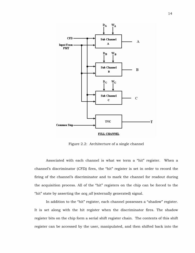
Each channel, illustrated in Figure 2.2, in this multi-channel IC is
composed of three sub-channels, a time-to-voltage converter (TVC), and read-out
related electronics. The three sub-channels are identical. The sub-channels
produce the three different integrations (A, B and C), and the TVC produces the
amplitude, T, that is proportional to the difference in time between the channel’s
discriminator firing and an external common stop reference.
14
Figure 2.2: Architecture of a single channel
Associated with each channel is what we term a “hit” register. When a
channel’s discriminator (CFDi) fires, the “hit” register is set in order to record the
firing of the channel’s discriminator and to mark the channel for readout during
the acquisition process. All of the “hit” registers on the chip can be forced to the
“hit” state by asserting the acq_all (externally generated) signal.
In addition to the “hit” register, each channel possesses a “shadow” register.
It is set along with the hit register when the discriminator fires. The shadow
register bits on the chip form a serial shift register chain. The contents of this shift
register can be accessed by the user, manipulated, and then shifted back into the

15
shadow register. By asserting an external signal, hit_transfer, it is possible to
transfer the contents of the shadow register to the hit register.
PSD8C supports three triggering modes. Figure 2.3 illustrates the triggering
logic located in the channel, and its operation is summarized in Table 2.2. The
Bypass (bypass the discriminator signal and use the EventEn to set timing) and
EventEn are externally generated signals. The CFDi signal is the discriminator
signal (externally generated) which is associated with the ith channel. The ChEni
signal is the channel enable for the ith channel. It is formed by ANDing the
GlobalEn signal with the appropriate channel enable bit in the configuration
register.
Figure 2.3: Trigger logic
Mode 1 Mode 2 Mode 3 Acq_All 1 (prior to readout) 0 0 Bypass 1 1 0 EventEn Timing signal for
start Timing signal for start
1
CFDi Ignore Sets the hit register Timing signal for start & sets the hit register
TVC Ignore Relative to CFDi Relative to CFDi
Table 2.2: Trigger modes

16
The trigger logic is designed to have considerable flexibility. The triggering
modes are described in detail below.
• MODE 1: The EventEn signal sets the timing for the start of the delay in the
sub-channels. In this mode all channels are then forced to be “hit” by
asserting the acq_all pin. The output of the TVC should be ignored since we
assume no need for a valid CFDi signal in this mode (acq_all sets hit
register). The Bypass signal should be HIGH in this mode.
• MODE 2: Then EventEn signal sets the timing for starting the delay in the
sub-channels. The CFDi signal for each channel sets the hit register for the
channel which was hit. TVC timing is relative to the CFDi signal. For Mode
2, EventEn needs to arrive prior to the CFDi signal for timing to be relative to
the CFDi signal. Note, the Bypass signal should be HIGH when using this
mode.
• MODE 3: CFDi sets the timing for starting the delay in the sub-channels. It
also sets the hit register for the channel that was hit. TVC timing is relative
to the CFDi signal. The Bypass signal should be held LOW in this mode.
For all modes, the TVC is always stopped by the “common stop” signal. In
addition to the three sub-channels, each channel contains a time-to-voltage
converter (TVC) as stated earlier. The TVC has two timing ranges, listed in Table
2.3.
17
Setting Range 0 2 μs default 1 500 ns
Table 2.3: TVC timing ranges
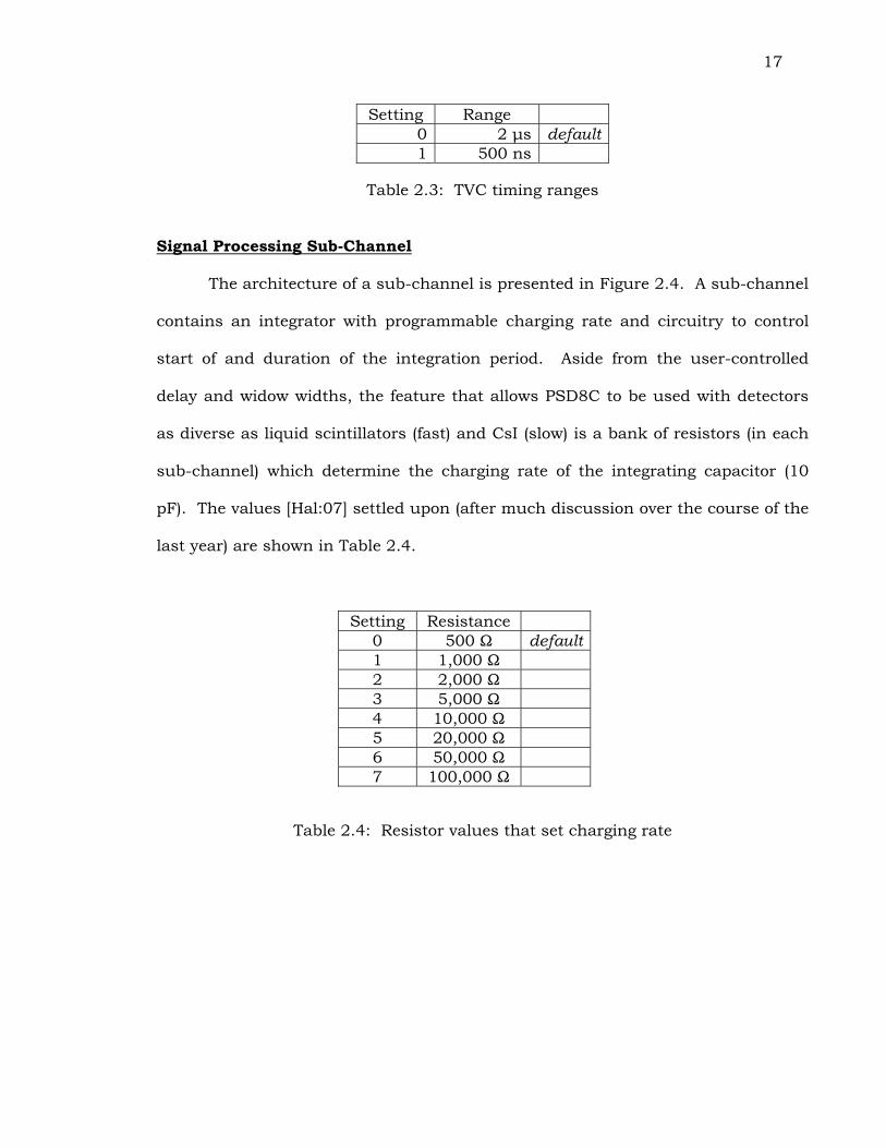
Signal Processing Sub-Channel
The architecture of a sub-channel is presented in Figure 2.4. A sub-channel
contains an integrator with programmable charging rate and circuitry to control
start of and duration of the integration period. Aside from the user-controlled
delay and widow widths, the feature that allows PSD8C to be used with detectors
as diverse as liquid scintillators (fast) and CsI (slow) is a bank of resistors (in each
sub-channel) which determine the charging rate of the integrating capacitor (10
pF). The values [Hal:07] settled upon (after much discussion over the course of the
last year) are shown in Table 2.4.
Setting Resistance 0 500 Ω default 1 1,000 Ω 2 2,000 Ω 3 5,000 Ω 4 10,000 Ω 5 20,000 Ω 6 50,000 Ω 7 100,000 Ω
Table 2.4: Resistor values that set charging rate

18
Figure 2.4: Sub-channel architecture
Initially, the integration capacitor is discharged (DUMP signal is active). The
firing of the channel’s CFD starts the delay generator on the left side of the figure.
The delay generator consists of a constant current source charging a capacitor
which produces a voltage linearly proportional to time. When this voltage equals
the externally applied control voltage, Dx (where x = A, B, or C), an analog
comparator fires and starts the second delay generator depicted in Figure 2.4.

19
The charging rate of the capacitor in the delay generators can be different for
each of the three sub-channels in keeping with our desire to have the three sub-
channels possess different ranges of delay and integration width. However, all A
sub-channels on a chip will have the same setting. The same is true of the B and
C sub-channels. While the delay within the range is controlled by an external
voltage, one of four ranges can be selected by the user. The time delay depends
upon both the range selected and the applied externally control voltage. The
ranges chosen (once again after much study over the past year) are presented in
Table 2.5 [Hal:07].
Setting Minimum Maximum 0 10 ns 50 ns default 1 30 ns 150 ns 2 120 ns 600 ns 3 2,000 ns 10,000 ns
Table 2.5: Delay and integration width ranges
When the delay generator on right-side of Figure 2.4 starts, the DUMP signal
is de-asserted. This starts the integrator. The integration period ends when the
output voltage of this second ramp equals the voltage, Wx, which determines the
width of the integration period for the sub-channel. The switch controlled by the
signal INTx in turn opens, disconnecting the charging resistor from the integrator
amplifier and forcing the integrator to “hold” its output voltage until it can be
sampled by an off-chip ADC. After the output voltage is read by the off-chip ADC,
both delay generators are reset and the integrating capacitor voltage dumped.
If the voltages are not read out within a user-specified window after the
event occurs, the channels are automatically reset. The duration of time before the

20
automatic reset occurs is determined by an externally supplied control voltage. It
can be set from a few hundred nanoseconds to many microseconds. See Figure 2.5.
0.1
1
10
100
1 2 3
Control Voltage (Volts)
Del
ay ( μ
sec)
4
Figure 2.5: Delay before auto-reset versus control voltage
Proof of Concept
The simulated responses of the chip (a) liquid scintillator (gamma - red,
neutron – blue) and (b) CsI (proton – red, alpha – blue) are shown in Figure 2.6.
The figure describes integrations in two different regions plotted against one
another as a function of deposited energy. The energies increase going up the
curves. These plots are for: (a) CsI(Tl) (proton – red, alpha – blue ) and (b) liquid
scintillator (gamma - red, neutron – blue). The B voltage (delayed gate) for the
liquid scintillator could be differentially amplified off chip before digitization. These
simulations model the time dependent detector outputs as the sums of
exponentials with particle dependent but energy independent parameters.
These crude simulations are at the symbolic math level and make use of
average (noiseless) signals deduced from devices built by the Washington
University group. In these simulations only the A and B sub-channels were needed

21
to clearly distinguish the waveforms (modeled by sums of exponential functions
with parameters determined from the real devices.) The interested reader is
referred to the Hall thesis [Hal:07] for additional details.
0 0.1 0.2 0.3 0.4 0.50
0.1
0.2
0.3
0.4
0.5
ProtonAlpha
B (V)
A(V
)a) CsI(Tl)
0 0.01 0.02 0.03 0.04 0.05 0.06 0.07 0.080
0.1
0.2
0.3
0.4
0.5
GammaNeutron
B (V)
A(V
)
b) Liquid Scintillator
Figure 2.6: Pulse-shape discrimination plots

22
CHAPTER 3
PSD8C CIRCUIT DESIGN
The PSD8C chip is composed of eight signal processing channels and a
“common” channel. The common channel provides support functions to the signal
processing channels. The IC is composed mostly of CMOS devices. Some of the
reference circuits, however, make use of a parasitic vertical PNP bipolar transistor.
The target technology is the AMIS 0.5 micron, NWELL process (C5N). The process
supports three metal layers, double-poly capacitors, and a high resistance poly
layer. The C5N process is a 5 Volt process.
The circuits described in this chapter were designed assuming the (nominal)
process parameters shown below:
VTN is threshold voltage of NFET = 0.75 Volts
VTP is threshold voltage of PFET = -1 Volts
KPN is transconductance parameter of NFET = 100 μA/V2
KPP is transconductance parameter of PFET = 32 μA/V2
KaN is 1/f noise parameter for NFET = 6.3 x 10⁻²⁶ A F
KaN is 1/f noise parameter for PFET = 3.8 x 10⁻³⁰ A F
Common Channel
The common channel consists of a bandgap voltage reference, biasing
circuits, buffer amplifiers (that permit us to drive off-chip electrical loads), readout
electronics, and a 48-bit configuration register. The functional blocks that make
up the common channel have been assembled, simulated, and physically layed
out.

23
The PSD8C’s 48-bit configuration register can be selectively loaded to
produce various control signals for the proper functioning of the IC. The output of
the configuration register can disable CFD outputs on a channel-by-channel basis,
select test modes, select processing for either positive or negative pulses, select
TVC measurement range, select a range for the on-chip gate generators, and assign
an 8-bit ID to the chip. The chip only responds when an externally applied chip
address matches the ID stored in the chip's configuration register. For additional
information on the logic design of the configuration register, see the thesis by
Sadasivam [Sad:02].
Biasing circuits
The biasing circuits are composed of a bandgap voltage reference and a
series of current sources. The current sources used to bias the various circuits on
the integrated circuit fall into two categories: PTAT and temperature-independent.
The PTAT (Proportional to Absolute Temperature) current sources are used for
biasing operational amplifiers, comparators, one-shot circuits, etc. Critical circuits
like the DACs (Digital-to-Analog Converters) used to correct offsets associated with
the integrators in the signal processing channels and the TVCs (Time-to-Voltage
Converters) used to make accurate relative timing measurements employ
temperature-independent current sources.
Bandgap voltage reference
A bandgap voltage reference provides both a temperature- and a supply-
independent 1.23 Volts [Gra:77]. The bandgap voltage is created by first
generating a current that is Proportional-To-Absolute-Temperature (PTAT) and then
passing the current (120 μA) through the series combination of a resistor and a
24
diode-connected parasitic, vertical PNP transistor [Raz:01]. This PTAT current
exhibits a positive temperature coefficient. The diode connected transistor base-
emitter voltage displays a negative temperature coefficient (-2mV/C).
When the output voltage is approximately 1.2 Volts, the output has near
zero temperature dependence. This bandgap voltage reference was also used in the
HINP16C integrated circuit (discussed in Chapter 1) and is well-tested. No
curvature correction is performed since a reference with modest performance is
sufficient for this application. Additional information regarding the design of the
bandgap circuit can be found in [Sad:02].
Current sources
By mirroring current from the PTAT current source in the bandgap
reference, six other PTAT currents were generated. One might ask why having
bias currents proportional to absolute temperature is beneficial? For weakly or
moderately inverted FETS, the device’s transconductance is linearly proportional to
bias current but inversely proportional to absolute temperature. By using PTAT
currents to bias a weakly or moderately inverted FET, the device transconductance,
gm, becomes independent of temperature [Raz:01]. Since op amp gain-bandwidth
products (GBW) depend on the gm of the input devices, the GBW of the op amp
displays little temperature dependence.
The mirrored currents were passed through diode-connected FETs and the
resulting bias voltages distributed throughout the IC. While distributing currents
is often preferred [Raz:01], distributing bias voltages requires less area. This is the
same technique that was employed in the HINP16C IC, and has worked well.
Table 3.1 summarizes the bias voltages distributed around the IC. The
name of the biasing node is given along with the current flowing through the diode-

25
connected FET. The size of the FET is also provided for easy reference (where m is
the number of parallel devices used). The name VB_INT appears twice. This is
because the value of the current is different depending upon the biasing mode the
user has selected in the chip’s configuration register. The HIGH bias mode is used
for fast detectors (Liquid scinitillator, for example) while the LOW bias mode is
more appropriate for use with slow detectors (CSI, for example).
Name Current Transistor size (W/L), μm
VB_INT 120 μA 4 / 5, m = 8
VBN_BUFFER 30 μA 19.2 / 19.2, m = 1
VBN_ONE_SHOT 30 μA 2.4 / 21.6, m = 6
VBN_CONST_I 30 μA 2.4 / 21.6, m = 6
VBN_CMP 30 μA 2.4 / 21.6, m = 5
Table 3.1: PSD8C biasing voltages
The VBN_BUFFER node is used to bias the op amps used in the buffers that
transmit analog voltages off chip. The VBN_ONE_SHOT node is used to bias the
various monostables employed in the signal processing channels. VBN_CONST_I is
used to bias the op amp that generates the temperature independent bias currents.
Finally, VB_CMP is used to bias the comparators that are used in the voltage-to-
time converters (VTCs).
Temperature-independent current sources
As stated above, some of the PSD8C circuits require bias currents that
display little or no temperature dependence. In order to produce temperature

26
independent currents, the 1.23 Volt output of the bandgap reference is applied to
the input of a transconductance amplifier built from an op amp and a temperature
independent resistor (123 kΩ). The temperature independent resistor was created
by placing two resistors in series. One resistor (85 kΩ), built using NY poly,
displays a positive temperature coefficient and the other resistor (38 kΩ), built
using HY poly, possesses a negative temperature coefficient. When combined in
the appropriate proportions, the resulting series connection exhibits a zero
temperature coefficient.
The resulting 10 μA (nominal) temperature-independent current is then
mirrored to create 4 bias currents. As with the PTAT currents, the currents are
passed through diode connected FETS to generate a bias voltage (see Table 3.2)
and these voltages are then distributed around the IC. In Table 3.2, the name of
the biasing node is given along with the current flowing through the diode-
connected FET. The size of the FET is also provided for easy reference.
Name Current Transistor size (W/L), μm
VB_TAC_10uA 10 μA 3.6 / 14.4, m = 2
VB_TAC_1uA 1 μA 3.6 / 14.4, m = 2
VBP_MULT 5 μA 19.2 / 2.4, m = 1
VBP_DAC 2 μA 2 / 4.6, m = 2
VB_TVC 10 μA 3.6 / 14.4, m = 2
Table 3.2: PSD8C temperature-independent biasing voltages

27
VB_TAC_1uA is used to bias the linear ramp generators used in the voltage-
to-time converters (VTCs). VBP_MULT is used to bias the “multiplicity” circuits in
each of the channels. The IC’s “multiplicity” output is an analog voltage which is
available at a pin. The voltage is proportional to the number of channels on the IC
whose CFDs have fired. The VB_TVC voltage is used to bias the time-to-voltage
circuits. Each of the eight channels contains a single TVC circuit.
VBP_DAC is used to bias the digital-to-analog converter (DAC) used to null
the integrator op amp offset voltage. Each sub-channel contains an integrator
whose offset is nulled by using a DAC. All of these DACs are biased using the
VBP_DAC voltage.
Readout electronics
The IC possesses readout circuits that present useful data to the outside
world. This includes the information on how many channels are hit, if any of the
channels are hit, an acknowledgement to indicate the completion of the acquisition
process, and the address of the channel currently being processed.
Output buffers
In order to transmit the analog voltages at the outputs of the A, B, and C
sub-channel integrators and the voltage at the output of the TVC (the T signal) off
chip, a buffer is required. The buffer was designed to drive a nominal load of 10 pF
and 10 KΩ. To improve performance and to make it easier to interface to a
differential input ADC, a decision was made perform the single-ended to differential
conversion on chip. Using a differential output to drive off chip will minimize
interference once the signal leaves PSD8C.

28
Core amplifier
The core amplifier is a two-stage design [Hog:94]. The first stage is a folded
cascade [Lak:94, Gre:86], and the second stage is a class-AB output stage. The
folded cascode has both a NFET and a PFET differential input pair. The use of
complementary differential input pairs provides the core amplifier with a near rail-
to-rail input common-mode range.
The class AB output stage is a complementary common-source amplifier
where the NFET serves as the load for the PFET and vice versa. To save area, the
class-AB driver circuit has been incorporated in the folded cascade summing
circuit. The floating architecture of the class-AB driver prevents it from
contributing to the noise and offset of the amplifier.
Single-ended-to-differential converter
The singled-ended-to-differential conversion circuit is comprised of two op
amps. One op amp connected as a unity-gain follower while the second as an
inverting gain amplifier with a gain of -1.
While the core amplifiers contain both a NFET and a PFET differential pair,
the polarity of the pulse is known. Bit 39 in the 48-bit configuration register sets
the desired polarity. This polarity bit is then used to select the desired input
differential pair. By only having one differential pair actually carrying signal, the
linearity of the buffer is dramatically improved. This is because the NFET
differential and PFET differential pairs will possess different DC offset voltages.
While a constant DC offset voltage does not present a problem, an offset voltage
that changes during the transient is undesirable and results in buffer non-
linearity. The unused input pair has its input shorted to analog signal ground

29
(AGND). In the case of the TVC buffer, the polarity is always positive so the NFET
differential pair is always selected.
Channel
Each channel is composed of a time-to-voltage converter (TVC) and three
sub-channels. All eight signal processing channels on the PSD8C chip are
identical.
Time-to-voltage converter
Associated with each channel on the IC is a discriminator signal that signals
the onset of the input pulse. The 8 discriminator signals are generated off chip,
typically by constant fraction discriminator (CFD) circuits [Sim:95, Sim:96, Sim:97]
built with off-the-shelf components. At some time in the future, these CFD circuits
could be incorporated on the PSD chip [Sad:02]. The CFD circuits were not
integrated on PSD8C because they would occupy a significant amount of area on
the IC, dissipate a lot of power, and reduce the flexibility of the IC [Sob:07]. The
CFD circuits are application specific. By leaving the CFD circuits off the chip, the
PSD8C micro-chip can be used by a larger group of experimenters.
In many experiments the relative timing between the arrival of the various
discriminator signals contains valuable information. The TVC circuit in each of the
channels permits us to measure the time between the arrival of the channel’s
discriminator signal and an externally generated common stop signal.
A constant current is used to charge a capacitor. The TVC is designed
[Sad:02] to operate in two different mode settings, the 250ns/Volt mode and the
2µs/Volt mode. The TVC can be switched between these two modes by changing

30
the bias voltage VB_TVC. The measurement is stored as an analog voltage across
a capacitor.
Hit logic
The hit logic [Sad:02] consists of two registers: the hit register and the active
register. The hit register gets set when the CFD fires, indicating that the channel
has been hit. This register is reset only when all the useful data from that
particular channel is readout or it can be forcibly reset by an external reset signal.
The data is readout from the channel only when a token is passed in to the
circuit and when the data is read this token is passed onto the next channel. This
token is passed channel-to-channel until it reaches the final channel in the chip.
This circuit consists of a pull-down transistor whose drain node is connected to the
same node in all channels and to a pull-up transistor, thus creating a pseudo-
NMOS type NOR gate.
The output from this node is an indication of at least one channel in the
chip being hit. It also houses a part of the total multiplicity circuit, from which one
can determine the number of channels that are hit. The multiplicity circuit
consists of just a current source that can be switched so as to source current into
a resistor connected to circuit ground. The multiplicity outputs from all of the
channels are connected in parallel.
Triggering logic
PSD8C supports 3 triggering modes. The triggering logic is illustrated in
Figure 3.1.

31
Figure 3.1: PSD8C triggering logic
Sub-Channel
Each sub-channel consists of a gated integrator and gate generator. The
gate generator is formed by a pair of externally programmable voltage-to-time
converters (VTC) that define the start and width of the integration period.
Gate generator
One VTC determines the start of the integration period relative to the
channel’s discriminator signal. The second VTC determines the duration of the
integration. As described in Chapter 2. Each channel consists of three sub-
channels, called A, B, and C. The start of the integration period for the A sub-
channel is set by an externally supplied voltage. Similarly, the period of integration
for all A sub-channels, is set by a second externally supplied voltage. The same
can be said for the B and C sub-channels.
The purpose of the VTC circuit is to produces a logic signal which is active
for a specified period of time. This period of time should be proportional to the
magnitude of the applied external voltage. The VTC consists of a ramp generator
and an analog comparator. When the VTC start signal is asserted, the ramp
generator output begins its linear rise. The output of the ramp generator is

32
continuously compared to the externally supplied voltage. When the comparator
output transitions high, the requested time has elapsed.
Comparator
A continuous-time comparator is merely an op amp running open-loop. A
folded-cascode OTA (operational transconductance amplifier) was chosen for the
core amplifier. It was designed to be fast and stable in the unity-gain
configuration. While stability is not generally a concern in comparator design, it
was in this application. Since the large input offset voltage of our core amplifier
cannot be tolerated, an auto-zeroing technique is used [All:03]. Initially the
comparator is placed in the unity gain configuration storing the offset on the auto-
zero capacitor, and then the comparator is switched into an open-loop
configuration with offset cancellation achieved at the non-inverting input.
Ramp generator
The ramp generator in the VTC is similar to the design used in the TVC
circuit. A current is used to charge a capacitor.
Integrator
The integrator in each of the sub-channels consists of three components: an
op amp, a resistor array, and the integrating capacitor.
Core op amp
The core amplifier is a two-stage design [Hog:94]. The first stage is a folded
cascade and the second stage is a class AB output stage. The class AB output

33
stage is a complementary common-source amplifier where the NFET serves as the
load for the PFET and vice versa.
The core op amp needed to meet the following specifications. The GBW
should be at least 50 MHZ. It should be able to supply several milli-amps of
output current and possess a near rail-to-rail output voltage swing. A slew rate of
at least 10 Volts/μsec was desired.
Resistor array
One of the features that permit the IC to be used with detectors as diverse
as liquid scintillators (fast) and CsI (slow) is a bank of resistors (in each sub-
channel) which determine the charging rate of the integrating capacitor. The
values settled upon (after much discussion over the course of the last year) are
shown in Table 3.3. The resistors are constructed from “HY” poly. HY poly is the
second layer poly that is doped so as to increase the sheet resistance. The HY
sheet resistance is typically 1 kΩ/square. All of the resistors in Table 3.3 are
constructed using a 1 kΩ unit resistor.
Setting Resistance 0 500 Ω default 1 1,000 Ω 2 2,000 Ω 3 5,000 Ω 4 10,000 Ω 5 20,000 Ω 6 50,000 Ω 7 100,000 Ω
Table 3.3: Resistor values

34
Integrating capacitor
Through extensive simulations [Hal:07], the optimum size for the integrating
capacitor was determined to be 10 pF. The total integrated noise, sqrt(kBT/C),
when C is 10 pF is 20 μV.
Offset-canceling DAC
As described above, the op amp used in the design of the integrator is
expected to have an input referred offset of approximately 10 mV (3 σ). Moreover,
mismatch between the signal ground and the input pulse DC baseline may
contribute an additional 5 mV. DC offsets are especially troublesome in integrator
applications because even a small DC input-referred offset can result in the output
of the integrator saturating if the integration time is long. In an attempt to
effectively reduce the magnitude of the input-referred offset, the non-inverting
terminal of the op amp used in the integrator is driven by the output of a 5-bit
DAC. The offset-canceling DAC uses a sign/magnitude data representation. The
most significant bit determines polarity while the lower 4 bits provide magnitude
information.
There are three architectures that Nyquist rate DACSs typically employ.
These three architectures are current scaling, voltage scaling, and charge scaling
[All:03]. A current scaling approach was adopted because for a small number of
bits (for example, 5, like in this application) current scaling DACs are generally the
most area efficient, consume very small amounts of power, and are simple to
design.
The current scaling DAC was realized using two binary weighted current
mirror arrays, one for positive polarity and the other for negative polarity outputs
[All:03]. With only 4 magnitude bits, matching requirements are modest and non-

35
monotonic behavior is not a problem if common-centroid layout techniques are
used in the layout of the DAC. The full-scale range of the DAC is typically 25 mV
with a step size of approximately 1.7 mV.
36
CHAPTER 4
SIMULATED PERFORMANCE OF PSD8C
Chapter 4 presents the results of simulations performed on the circuits
comprising PSD8C. Simulations which demonstrate that the entire chip functions
correctly are also included. The simulated performance represents a best-case
scenario as the simulations do not account for random offsets that will be present
when the IC is fabricated. However, analyses were performed to estimate the effects
of random offsets. The results of these analyses, when available, are also
presented.
Common Channel
The common channel contains the configuration register, the biasing
circuitry, and the output circuits. Testing of the configuration circuitry is reserved
for the full-chip simulations. The performance of the biasing circuits is dictated by
the quality of the bandgap and current references. The output buffers are used to
converter from a single-ended to a differential output.
Bandgap
The bandgap voltage produces a stable temperature-independent 1.2 Volts.
Since the bandgap reference was re-used, the interested reader is referred to
[Sad:02] for detailed simulations of the performance of the bandgap reference. The
circuit has been used in several integrated circuits designed in our research lab
over the past few years and functions well.

37
Current references
The current references are modified versions of those used in the HINP16C
design. The bias voltages generated can be classified into normal and temperature-
independent bias voltages. The performance of the various current references can
also be found in the HINP16C documentation [Sad:02].
Output buffer
The performance of the single-ended-to-differential output buffer used to
drive off-chip electrical loads is in large part determined by the performance of the
core amplifier used to implement the buffer. As discussed in Chapter 3, the output
buffer core amplifier possesses two input stages (an NFET and a PFET differential
pair). The “polarity” bit in the configuration register determines which input
differential pair is used. The NFET input stage is used for passing signals more
positive than AGND (2.5 Volts) while the PFET stage is use for passing signals
below AGND.
The total integrated noise of the buffer core amplifier is 142 µV when the
PFET input stage is used and 172 μV when the NFET input stage is used. The
buffer characteristics are very similar for the two polarities. The output load was
10 pF in parallel with 10 kΩ. The following sections discuss the frequency
response and linearity of the buffer.
Frequency response
The gain and phase plots for the output buffer (when using the PFET stage)
are presented in Figure 4.1. An additional 180° was added to the phase plot to
make it more readable. When the PFET input stage is used, the GBW of the core
amplifier used in the buffer is 3.5 MHz and the phase margin is 61°. The low-
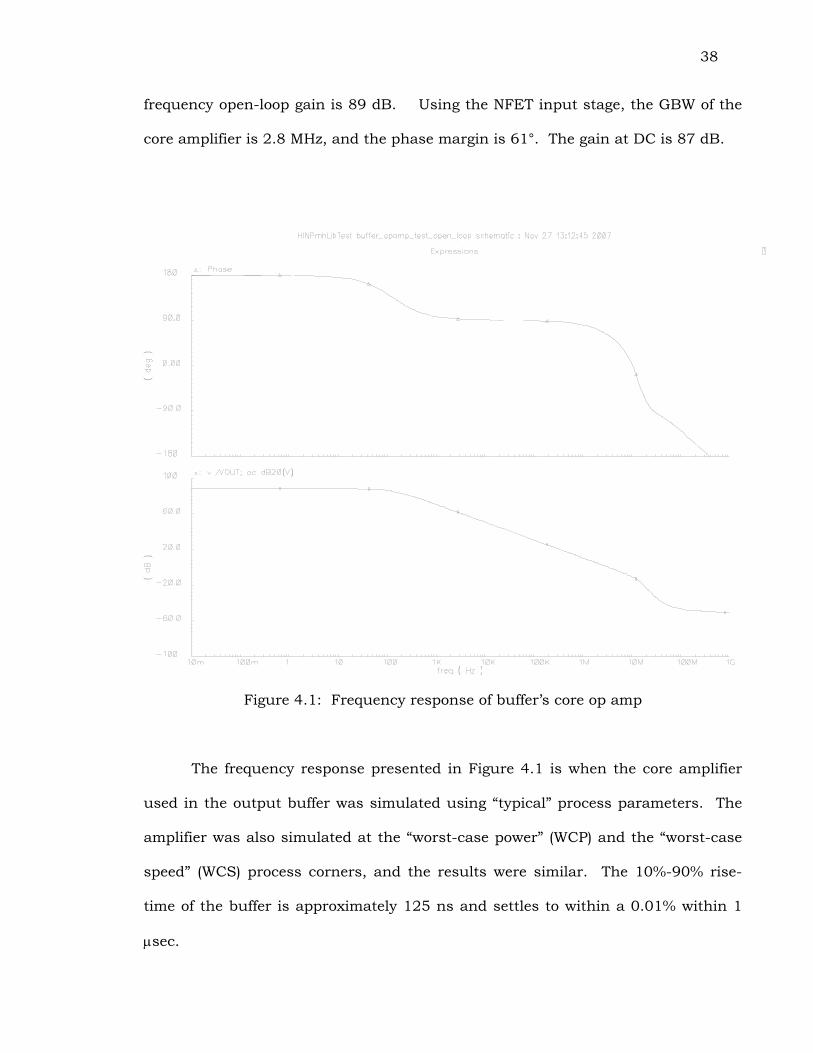
38
frequency open-loop gain is 89 dB. Using the NFET input stage, the GBW of the
core amplifier is 2.8 MHz, and the phase margin is 61°. The gain at DC is 87 dB.
Figure 4.1: Frequency response of buffer’s core op amp
The frequency response presented in Figure 4.1 is when the core amplifier
used in the output buffer was simulated using “typical” process parameters. The
amplifier was also simulated at the “worst-case power” (WCP) and the “worst-case
speed” (WCS) process corners, and the results were similar. The 10%-90% rise-
time of the buffer is approximately 125 ns and settles to within a 0.01% within 1
μsec.
39
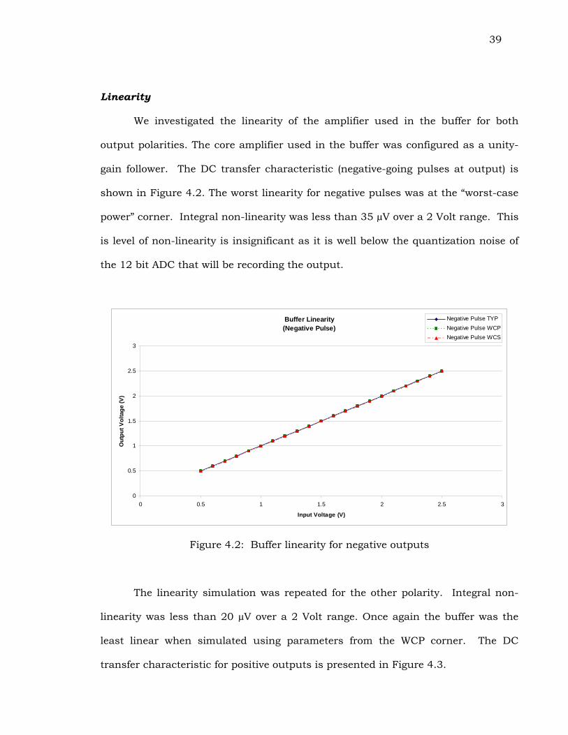
Linearity
We investigated the linearity of the amplifier used in the buffer for both
output polarities. The core amplifier used in the buffer was configured as a unity-
gain follower. The DC transfer characteristic (negative-going pulses at output) is
shown in Figure 4.2. The worst linearity for negative pulses was at the “worst-case
power” corner. Integral non-linearity was less than 35 µV over a 2 Volt range. This
is level of non-linearity is insignificant as it is well below the quantization noise of
the 12 bit ADC that will be recording the output.
Buffer Linearity(Negative Pulse)
0
0.5
1
1.5
2
2.5
3
0 0.5 1 1.5 2 2.5
Input Voltage (V)
Out
put V
olta
ge (V
)
3
Negative Pulse TYPNegative Pulse WCPNegative Pulse WCS
Figure 4.2: Buffer linearity for negative outputs
The linearity simulation was repeated for the other polarity. Integral non-
linearity was less than 20 µV over a 2 Volt range. Once again the buffer was the
least linear when simulated using parameters from the WCP corner. The DC
transfer characteristic for positive outputs is presented in Figure 4.3.

40
Buffer Linearity(Positive Pulse)
2
2.5
3
3.5
4
4.5
5
2 2.5 3 3.5 4 4.5 5
Input Voltage (V)
Out
put V
olta
ge (V
)
Positive Pulse TYPPositive Pulse WCPPositive Pulse WCS
Figure 4.3: Buffer linearity for positive outputs
Signal Processing Channel
The two items at the channel level that were evaluated were the linearity of
the integrator and the linearity of the TVC circuit used for relative timing
measurements.
Integrator linearity
Integrator linearity was investigated by generating pulse waveforms
representative of proton particles with known energy levels at the input of the
channel and recording the resulting integrator outputs. Linear regressions were
run on each dataset and the datasets were compared to the regression to
determine linearity. The channel was setup to integrate over common regions. The
integration regions were consistent with those that one might used if the chip were
to be used with CsI(Tl) detectors.

41
Recall that PSD8C can be used in one of two biasing modes: low-bias or
high-bias. The simulated data points differed from the best-fit line by no more
than 14μV in low bias mode and by no more than 11 μV in high-bias mode for the
3 process corners that were investigated. The transfer characteristic is presented
in Figure 4.4.
Particle Energy vs Channel Output Voltage
1.7
1.8
1.9
2
2.1
2.2
2.3
2.4
2.5
0 20 40 60 80 100
Energy (MeV)
Cha
nnel
Out
put V
olta
ge (V
)
120
Typical CsI Low BiasTypical CsI High Bias
Figure 4.4: Integrator linearity for low- and high-bias modes
The linearity of the channel was also investigated to see how sensitive the
characteristic was to process variations. The effect that process variations have on
linearity is illustrated in Figure 4.5. While the transfer characteristic (slope and
intercept) is a function of the process corner, this is not important since the
channels can be calibrated if total pulse-height information is desired using a
source of known energy. The slopes are different largely because of the process
variations in the sheet resistance of the material used to implement the integrating
resistor and variations in the capacitance per unit area of the integrating capacitor.

42
Particle Energy vs Channel Output Voltage
1.25
1.45
1.65
1.85
2.05
2.25
2.45
2.65
0 20 40 60 80 100 120
Energy (MeV)
Cha
nnel
Out
put V
olta
ge (V
)
Typical CsIWCP CsIWCS CsI
Figure 4.5: Integrator linearity as function of process corner
Moreover, in many of the applications (for example, particle identification
using PSD) the ratio of integrator outputs will be used. One would expect much
less channel-to-channel variation where matching of components is expected to be
quite good.
TVC linearity
The TVC’s linearity was also investigated. Recall that the TVC circuit was
designed to have two time ranges: 500 ns and 2 μs. The transfer characteristic for
the TVC circuit in the 500 ns mode is presented in Figure 4.6. Differences in the
slope (due to variations in process parameters) can be calibrated out for this circuit
as well.

43
TVC Linearity
1
1.2
1.4
1.6
1.8
2
2.2
2.4
2.6
0 100 200 300 400 500 600
Time (ns)
TVC
Out
put V
olta
ge (V
)
500ns TYP
500ns WCP
500ns WCS
Figure 4.6: TVC linearity in 500ns mode
Precision timing is very important in the applications where the PSD8C chip
will be used. Thus, the TVC circuit needs to be both monotonic and very linear.
Under “typical” (TYP) and WCS corners, linearity over the entire desired range is
not a problem. However, with the WCP corner, the circuit is highly linear to only
340 ns. Using this specification, the maximum deviation is 34 μV, which
corresponds to about 20ps. The TVC output starts to go nonlinear above an
output voltage just short of 2 Volts.
In the 2 μs mode (see Figure 4.7) the circuit is linear over its entire intended
range for both the TYP and WCS corners. However, the WCP corner once again
causes problems. A maximum deviation corresponding to 58 ps can be attained if
the TVC is limited to 1.2 μs (short of the desired 2 μs) at the WCP corner.
44
TVC Linearity
1
1.2
1.4
1.6
1.8
2
2.2
2.4
2.6
0 500 1000 1500 2000
Time (ns)
TVC
Out
put V
olta
ge (V
)
2us TYP
2us WCP
2us WCS
Figure 4.7: TVC linearity in 2 μs mode
Signal-Processing Sub-Channel
The sub-channel contains three major components: the DAC, the gate
generator, and the integrating op amp. The DAC is needed to compensate for
random DC offsets associated with integrator op amp and to deal with small errors
in the input waveform baseline if the inputs are DC-coupled. In many applications
the inputs to the chip will be AC-coupled. The random DC offset of the integrator
op amp is estimated not to exceed 10 mV. Hence, a nominal range of +/- 20 mV
was sought for the DAC. The gate generator is used to create the integrations
regions. It consists of pair of voltage-to-time converters (VTCs).

45
DAC
The DAC has a positive and a negative range corresponding to inputs of 0 to
15 and -0 to -15 respectively. Zero and negative zero both give identical outputs of
0V.
DAC range
The full range of the DAC was simulated over the “typical”, “worst-case-
power”, and “worst-case-speed” process corners. The transfer characteristic for the
DAC is shown in Figure 4.8. Under the worst-case conditions the range will still
exceed +/- 15 mV.
DAC Range
-0.025
-0.020
-0.015
-0.010
-0.005
0.000
0.005
0.010
0.015
0.020
0.025
-16 -12 -8 -4 0 4 8 12 16
Input
Out
put (
V)
DAC TYP DAC WCPDAC WCS TYP TrendWCP Trend WCS Trend
Figure 4.8: DAC range
The integral nonlinearity error was less than 1/4 of a least significant bit
(LSB) across process corners. The differential nonlinearity error was less than

46
1/10 LSB. Analyses predict that the error due to random offsets will be less than
¼ LSB.
DAC Temperature Dependence
The DAC was tested over a temperature range of 0 C to 80 C. The
temperature dependence of the DAC is illustrated in Figure 4.9. The DAC’s output
voltage exhibits a temperature coefficient of -8 µV per degree Celsius.
DAC Temperature Dependence
0.01900
0.01910
0.01920
0.01930
0.01940
0.01950
0.01960
0.01970
0.01980
-10.00 0.00 10.00 20.00 30.00 40.00 50.00 60.00 70.00 80.00 90.00
DAC Input
DAC
Out
put (
V)
DAC(15) TYP
Figure 4.9: DAC temperature dependence
VTC
The gate generator in each sub-channel is constructed from a pair of VTCs.
The VTC circuit has four modes or ranges. Recall, PSD8C requires 6 (DA, DB, DC,
WA, WB, WC) externally generated TVC control voltages. These voltages determine
the delay. Linearity is less important than in the TVC, since the controlling

47
voltages are external to the chip so they can be adjusted to get the desired regions.
A signal that is high while the integrator is integrating the input signal is available
at one the PSD8Cs pins (see Appendix B). These sub-channel signals are
multiplexed so this integration signal for each of the sub-channels on the chip can
be inspected.
VTC range and linearity
The VTC was simulated for each mode with control voltages in the range of
0V to 2.5V at a temperature of 20 C. Table 4.1 shows the time range that can be
attained in Mode 0 (as a function of process corner) for control voltages of 0.5 Volts
and 2.5 Volts. The table also provides the conversion factor between elapsed time
and applied voltage (Dx or Wx).
Delay (ns)
Vc (V) TYP WCP WCS 0.5 31.49 24.24 40.22 2.5 68.14 55.13 82.63
ns/V 5 5 5 18.32 15.44 21.20
Table 4.1: VTC conversion factor (Mode 0)
The VTC is linear in Mode 0 for control voltages between 0.5 V and 2.5 V. The
transfer characteristic for the VTC (Mode 0) is presented in Figure 4.10.
48
Reference Voltage vs Delay Time
0
10
20
30
40
50
60
70
80
90
-0.25 0 0.25 0.5 0.75 1 1.25 1.5 1.75 2 2.25 2.5 2.75
Control Voltage (V)
Tim
e (n
s)
Typical
Worst Case Power
Worst Case Speed
Figure 4.10: VTC transfer characteristic (Mode 0)
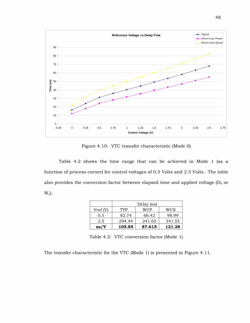
Table 4.2 shows the time range that can be achieved in Mode 1 (as a
function of process corner) for control voltages of 0.5 Volts and 2.5 Volts. The table
also provides the conversion factor between elapsed time and applied voltage (Dx or
Wx).
Delay (ns) Vref (V) TYP WCP WCS
0.5 82.74 66.42 98.99 2.5 294.44 241.65 341.55
ns/V 105.85 87.615 121.28
Table 4.2: VTC conversion factor (Mode 1) The transfer characteristic for the VTC (Mode 1) is presented in Figure 4.11.

49
Reference Voltage vs Delay Time
0
50
100
150
200
250
300
350
400
-0.25 0 0.25 0.5 0.75 1 1.25 1.5 1.75 2 2.25 2.5 2.75
Control Voltage (V)
Tim
e (n
s)
Typical
Worst Case Power
Worst Case Speed
Figure 4.11: VTC transfer characteristic (Mode 1)
Table 4.3 shows the time range that can be attained in mode 2 (as a
function of process corner) for control voltages of 0.5 Volts and 2.5 Volts. The table
also provides the conversion factor between elapsed time and applied voltage (Dx or
Wx). The transfer characteristic for the VTC (Mode 2) is presented in Figure 4.12.
Delay (ns) Vref (V) TYP WCP WCS
0.5 351.43 284.97 410.64 2.5 1570.22 1293.87 1807.53
ns/V 609.40 504.45 698.45
Table 4.3: VTC conversion factor (Mode 2)

50
Reference Voltage vs Delay Time
0
200
400
600
800
1000
1200
1400
1600
1800
2000
-0.25 0 0.25 0.5 0.75 1 1.25 1.5 1.75 2 2.25 2.5 2.75
Control Voltage (V)
Tim
e (n
s)
Typical
Worst Case Power
Worst Case Speed
Figure 4.12: VTC transfer characteristic (Mode 2)
Table 4.4 shows the time range that can be attained in mode 3 (as a
function of process corner) for control voltages of 0.5 Volts and 2.5 Volts. The table
also provides the conversion factor between elapsed time and applied voltage (Dx or
Wx). The transfer characteristic for the VTC (Mode 3) is presented in Figure 4.13.
Delay (ns)
Vref (V) TYP WCP WCS 0.5 2198.78 1793.27 2536.97 2.5 10648.14 8728.68 12226.97
ns/V 4224.7 3467.7 4845.0
Table 4.4: VTC conversion factor (Mode 3)
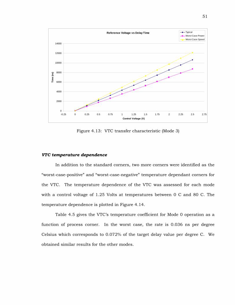
51
Reference Voltage vs Delay Time
0
2000
4000
6000
8000
10000
12000
14000
-0.25 0 0.25 0.5 0.75 1 1.25 1.5 1.75 2 2.25 2.5 2.75
Control Voltage (V)
Tim
e (n
s)
TypicalWorst Case Power
Worst Case Speed
Figure 4.13: VTC transfer characteristic (Mode 3)
VTC temperature dependence
In addition to the standard corners, two more corners were identified as the
“worst-case-positive” and “worst-case-negative” temperature dependant corners for
the VTC. The temperature dependence of the VTC was assessed for each mode
with a control voltage of 1.25 Volts at temperatures between 0 C and 80 C. The
temperature dependence is plotted in Figure 4.14.
Table 4.5 gives the VTC’s temperature coefficient for Mode 0 operation as a
function of process corner. In the worst case, the rate is 0.036 ns per degree
Celsius which corresponds to 0.072% of the target delay value per degree C. We
obtained similar results for the other modes.
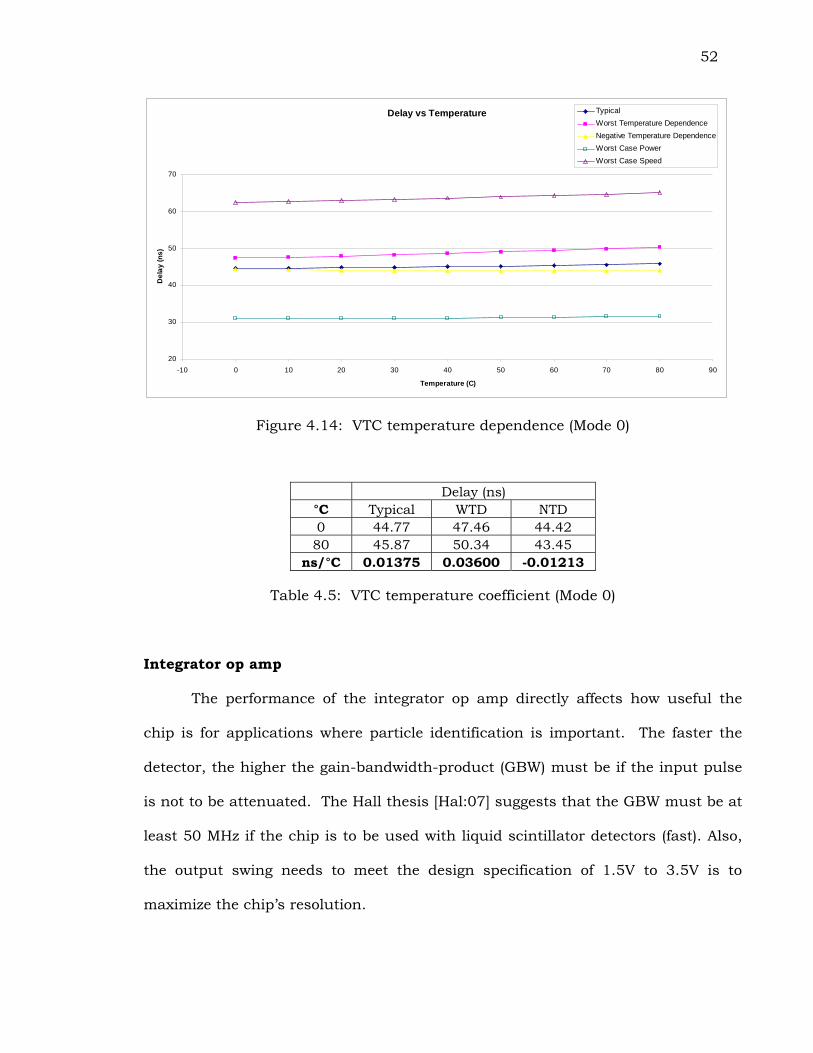
52
Delay vs Temperature
20
30
40
50
60
70
-10 0 10 20 30 40 50 60 70 80 90
Temperature (C)
Del
ay (n
s)
TypicalWorst Temperature DependenceNegative Temperature DependenceWorst Case PowerWorst Case Speed
Figure 4.14: VTC temperature dependence (Mode 0)
Delay (ns)
°C Typical WTD NTD 0 44.77 47.46 44.42 80 45.87 50.34 43.45
ns/°C 0.01375 0.03600 -0.01213
Table 4.5: VTC temperature coefficient (Mode 0)
Integrator op amp
The performance of the integrator op amp directly affects how useful the
chip is for applications where particle identification is important. The faster the
detector, the higher the gain-bandwidth-product (GBW) must be if the input pulse
is not to be attenuated. The Hall thesis [Hal:07] suggests that the GBW must be at
least 50 MHz if the chip is to be used with liquid scintillator detectors (fast). Also,
the output swing needs to meet the design specification of 1.5V to 3.5V is to
maximize the chip’s resolution.

53
Frequency response
The frequency response of the op amp is plotted under typical corner
parameters (TYP) in Figure 4.15. In low bias mode, the GBW is about 18MHz, and
the phase margin is 70 degrees (5 pf capacitive load). The low-frequency
differential mode gain exceeds 90 dB. As we demonstrate in the channel
simulations later in this chapter, this is sufficient to discriminate slower particles
and can be used with CsI detectors. In high bias mode, the GBW is 50 MHz, while
the phase margin remains around 70 degrees. The differential mode gain drops to
about 80dB, which is sufficiently high (> 50 dB) [Hall:07] for this application.
Figure 4.15: Frequency response of the integrating op amp

54
Output voltage swing
The output swing, of the integrating op amp, under typical corner
parameters is 0.5 Volts to 4.5 Volts. Regardless of process corner, the output
range is never smaller than 0.7 Volts to 4.3 Volts. This exceeds our 1.5 Volts to
3.5 Volts specification.
Noise performance
The total integrated thermal noise of the integrating op amp remains below
90µV in the worst case. The total integrated 1/f noise between 0 and 1 GHz is 116
µV. Since uncorrelated noise sources add in quadrature, the total integrated noise
op the op amp is 145 µV.
Chip
The PSD8C chip inherited much of the read-in and read-out electronics from
the HINP16C chip. Because of this, scripts were made for both chips that required
minimal modification to work on either. The PSD8C chip is smaller, but similarly
shaped to the HINP16C. A 16 channel version of the chip would end up in a
roughly square configuration.
Configuring chip
The configuration registers were checked by simulating several configuration
scenarios. We then checked the configuration register to make sure the correct
settings were stored. Since most of the circuitry is identical to the HINP16C’s
circuitry, only a few simulations were performed
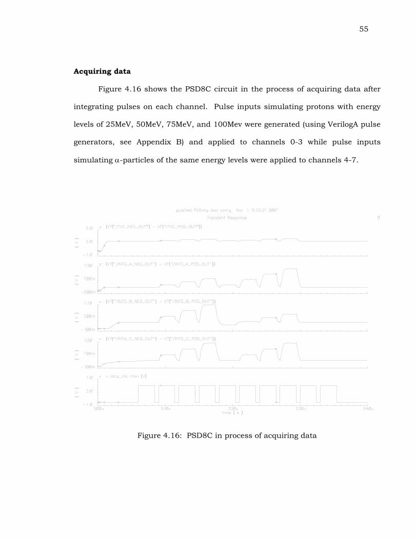
55
Acquiring data
Figure 4.16 shows the PSD8C circuit in the process of acquiring data after
integrating pulses on each channel. Pulse inputs simulating protons with energy
levels of 25MeV, 50MeV, 75MeV, and 100Mev were generated (using VerilogA pulse
generators, see Appendix B) and applied to channels 0-3 while pulse inputs
simulating α-particles of the same energy levels were applied to channels 4-7.
Figure 4.16: PSD8C in process of acquiring data
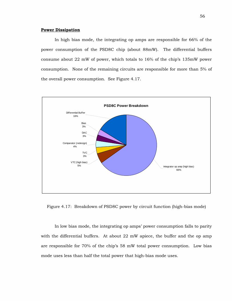
56
Power Dissipation
In high bias mode, the integrating op amps are responsible for 66% of the
power consumption of the PSD8C chip (about 88mW). The differential buffers
consume about 22 mW of power, which totals to 16% of the chip’s 135mW power
consumption. None of the remaining circuits are responsible for more than 5% of
the overall power consumption. See Figure 4.17.
Integrator op amp (high bias)66%
Differential Buffer16%
Bias3%
DAC3%
TVC3%
Comparator (redesign)4%
VTC (high bias) 5%
PSD8C Power Breakdown
Figure 4.17: Breakdown of PSD8C power by circuit function (high-bias mode)
In low bias mode, the integrating op amps’ power consumption falls to parity
with the differential buffers. At about 22 mW apiece, the buffer and the op amp
are responsible for 70% of the chip’s 58 mW total power consumption. Low bias
mode uses less than half the total power that high-bias mode uses.

57
Integrator op amp (low bias)35%
Differential Buffer35%
Bias7%
DAC7%
TVC7%
Comparator (redesign)8%
VTC (low bias) 1%
PSD8C Power Breakdown
Figure 4.18: Breakdown of PSD8C power by circuit function (low-bias mode)
Area Distribution
The total area of PSD8C is 15.5 mm2. The common circuitry, which
contains the configuration, biasing and output circuitry, takes up about 19% of
this area. The eight channels account for the remaining 81% of the area. Each
channel consists of a TVC, hit logic, and three sub-channels.
The area breakdown for a single channel is shown in the left pie graph of
Figure 4.19. The largest portion of the channel is made up of the three sub-
channels (as one might expect!). The right pie graph in of Figure 4.22 shows the
breakdown of the sub-channel into its major components. These components in
order of size are the VTC, DAC, integrating op amp, integrating resistors, and
integrating capacitor.

58
Integrating Op Amp13%
DAC22%
VTC31%
Integrating Resistors7%
Integrating Capacitor8%
TVC11%
Hit Logic8%
Subchannel81%
PSD8C Channel Area Breakdown
Figure 4.19: Breakdown of PSD8C area by circuit function
Layout of Chip
The layout of the PSD8C chip (2748 μm x 5659 μm) is presented in Figure
4.20. The physical layout of the IC was performed by graduate students Danesh
Dasari and Nagendra Valluru. The biasing and circuits used for configuring the IC,
as well as for readout, are located in the center (“common” channel) of the chip.
The signal processing channels are arranged in four quadrants. Each quadrant
contains two channels but can be easily extended to four channels to
accommodate PSD16C at some time in the future. Channels 0 and 1 occupy the
lower-left quadrant while channels 1 and 2 occupy the lower-right quadrant.
Channels 3 and 4 occupy the upper-right quadrant and channels 6 and 7 occupy
the upper-left quadrant.

59
Figure 4.20: Final layout of PSD8C

60
The IC will be fabricated through MOSIS (MOS Implementation Services) at a
cost of approximately $10,000 (40 packaged parts). The parts will be packaged in
a LQFP128A plastic package, which is a 14 x 14 mm, 128 lead
thin quad flat pack. The pin-out for PSD8C is in Appendic B and the bonding
diagram is included in Appendix C.

61
CHAPTER 5
SUMMARY/FUTURE WORK
Summary
The PSD8C was designed to complement an existing shaped and peak-
sensing analog chip, called HINP16C (also, designed by this research laboratory).
PSD8C will be used in experiments where particle identification using pulse-shape
discrimination (PSD) is needed. The IC can provide total pulse-height information
as well so it is will be useful in a wide variety of experiments where modest energy
information is needed and particle identification is not required. The analog
approach the PSD8C has taken offers many benefits over current digital and
discrete analog approaches including:
Lower power
Smaller size
Lower cost (per channel)
High level of integration providing an increased level of reliability
Efficient data sparsification
Built-in high quality timing circuitry
Each of the eight channels is composed of a time-to-voltage converter (TVC) with
two time ranges (0.5 μsec, 2 μsec) and three sub-channels. Each of the sub-
channels consists of a gated integrator with 8 programmable charging rates and a
pair of externally programmable gate generators that define the start (with 4 time
ranges) and width (with 4 time ranges) of the gate relative to an external
discriminator signal. The chip supports 3 triggering modes.

62
The IC produces four sparsified analog pulse trains (3 integrator outputs
and 1 TVC output) with synchronized addresses for off-chip digitization with a
pipelined ADC. PSD8C, with two bias modes occupies an area of approximately
2.8 mm x 5.7 mm and has an estimated power dissipation of 135 mW in the high-
bias mode. The chip is to be fabricated in the AMIS 0.5-micron NWELL process
(C5N).
Conclusions
Simulations demonstrate that the PSD8C should work very will when used
with CsI (slow) and liquid scintillator (fast) detectors. The IC layout is complete,
and the design is ready for an early 2008 submission!
Future Work
The PSD8C will be sent out for fabrication in early 2008. Before the IC is
submitted to MOSIS (MOS Implementation Services), there are still a small set of
simulations that need to be performed. While the op amp used in the integrator
simulates correctly at the typical process corner, cascode devices in the first stage
enter the resistive region at the “worst-case-power” and the “worst-case-speed”
process corners. When these devices enter the resistive region, the op performance
is compromised. Small design changes will need to be made so that these devices
remain saturated. Simulations must still be performed that confirm correct
operation of the 3 triggering modes.
When the chip returns, it must be tested to make sure everything works as
simulated. New simulations will need to be done to understand any discrepancies.
Such simulations, could also give an idea as to what corner parameters the chip

63
most closely resembles, and thus what settings will provide the best results. Once
any deficiencies are addressed, the chip may be re-fabricated in 16 channel form.
Matlab code exists to help the user of the chip choose optimal integration regions.
Further work could be done on this code to increase flexibility, accuracy, or ease of
use. Another variation of the chip will be designed to support more integration
regions for use in handheld radiation detectors.
64
REFERENCES
[All:03] Phillip E. Allen and Douglas R. Holberg, CMOS Analog Circuit Design,
Second Edition, Oxford University Press, (2003). [Che:05] Lie-Wen Chen, Che Ming Ko, and Bao-An Li, Phys. Rev. Lett. 94,
032701 (2005). [Des:90] R. DeSouza, et al., Nucl. Instr. and Meth. A 295, 109 (1990). [Eng:06] G. Engel, L. Sobotka, and M. Famiano, NSF-MRI proposal (Jan.
2006). Available online at www.ee.siue.edu/~gengel/PSD.htm. [Eng:07] G. Engel, M. Sadasivam, M. Nethi, J. M. Elson, L.G. Sobotka and R.
J. Charity, “Multi-Channel Integrated Circuit for Use in Low and Intermediate Energy Nuclear Physics - HINP16C” in Nucl. Instru. Meth. A573, 418-426, (2007).
[Gra:77] Paul R. Gray and Robert G. Meyer, Analysis and Design of Analog
Integrated Circuits, John Wiley & Sons, Inc. (1977). [Gre:86] Roubik Gregorian and Gabor C. Temes, Analog MOS Integrated
Circuits for Signal Processing, Wiley-Interscience Publication. (1986.) [Hal:07] M. Hall, “Design Considerations in Systems Employing Multiple
Charge Integration for the Detection of Ionizing Radiation” SIUE EE M.S. Thesis, (2007).
[Hog:94] Ron Hogervorst, John P. Tero, Ruud G. H. Eschauzier, and Johan H.
Huijsing, “A Compact Power-Efficient 3-V CMOS Rail-to-Rail Input/Output Operational Amplifier for VLSI Cell Libraries”, IEEE Journal of Solid State Circuits, Vol.29, No.12, December 1994.
[Hor:01] C.J. Horowitz and J. Piekarewicz, Phys. Rev. Lett. 86, 5647 (2001). [Lak:94] Kenneth R. Laker and Willy M. C. Sansen, Design of Analog Integrated
Circuits and Systems, McGraw-Hill, Inc. 1994. [Lat:04] J. M. Lattimer and M. Prakash, Science 304, 536 (2004). [Lee:02] T. H. Lee, G. Cho, S.W. Lee, W. Lee, and S. H. Han, “Analysis of 1/f
Noise in CMOS Preamplifier with CDS Circuit”, IEEE Transactions on Nuclear Science, Vol.49, No.4, August 2002.
[OCo:99] P. O’Connor and G. De Geronimo, Brookhaven National Laboratory,
“Prospects for Charge Sensitive Amplifiers in Scaled CMOS”, Nuclear Science Symposium, 1999, Vol.1 , 24-30, October 1999, pages 88-93.
[Pon :02] J. Pons, et al., Applied Journal of Physics, 564, 981 (2002).

65
[Raz:92] B. Razavi, B.A. Wooley, “A 12 b 5Msample/s Two-Step CMOS A/D Converter”, JSSC, Vol. 27, No. 12, 1667-1678 (1992).
[Raz:01] B. Razavi, Design of Analog CMOS Integrated Circuits, McGraw Hill, (2001).
[Sae:96] Trond Saether, Chung-Chih Hung, Zheng Qi, Mohammed Ismail, and
Oddavar Aaserud, “High Speed, High Linearity CMOS Buffer Amplifier”, IEEE Journal of Solid-State Circuits, Vol.31, No.2, February 1996.
[Sad:02] M. Sadasivam, “A Multi-channel Integrated Circuit For Use With
Silicon Strip Detectors In Experiments In Low and Intermediate Physics,” SIUE EE M.S. Thesis, (2002).
[Sar:90] D. W. Stracener, et al., Nucl. Instr. and Meth. A 294, 485 (1990). [Sar:96] D.G. Sarantites, et al., Nucl. Instr. and Meth. A 381, 418 (1996). [Sar:04] D.G. Sarantites, et al., Nucl. Instr. and Meth., A530, 473 (2004). [Sha:64] I.I. Shapiro, Phys. Rev. Lett. 26, 789 (1964). [Sim:95] M.L. Simpson, C.L.Britton, A.l. Wintenberg and G.R. Young, Oak
Ridge National Laboratory, “An Integrated, CMOS, Constant-Fraction Timing Discriminator for Multichannel Detector Systems”, IEEE Transactions on Nuclear Science, Vol.42, No.4, August 1995.
[Sim:96] M.L. Simpson and G.R. Young, Oak Ridge National Laboratory, R.G.
Jackson and M.Xu, University of Tennessee, Knoxville, “A Monolithic, Constant-Fraction Discriminator Using Distributed R-C Delay Line Shaping”, IEEE Transactions on Nuclear Science, Vol.43, No.3, June 1996.
[Sim:97] Michael L. Simpson, Charles L. Britton, Alan L.Wintenberg, and
Glenn R.Young, “An Integrated CMOS Time Interval Measurement System with Sub nanosecond Resolution for the WA-98 Calorimeter”, IEEE Journal of Solid- State Circuits, Vol.32, No.2, February 1997.
[Sob:07] Personal communication with Dr. Lee Sobotka, Professor, Chemistry
Department, Washington University, Saint Louis. [Spi:05] Helmut Spieler, Semiconductor Detector Systems, Oxford University
Press, (2005). [Ste:89] A.E. Stevens, R.P. Van Berg, J. V. Van Der Spiegel, and H.H.
Williams, “A Time-to-Voltage Converter and Analog Memory for Colliding Beam Detectors”, IEEE Journal of Solid State Circuits, Vol. 24, No. 6, December 1989.

66
[Wal:07] M.S. Wallace, M.A. Famiano, M.J. van Goethem, A. Rogers, W.G. Lynch, J. Lee, S. Labostov, M. Macko, L. Morris, B.E. Nett, D.J. Oostdyk, R. Krishnasamy, M.B. Tsang, R.D. deSouza, S. Hudan, L.G. Sobotka, R.J. Charity, J. Elson, and G.L. Engel, “The High Resolution Array (HiRA) for rare isotope beam experiments”, in Nucl. Instru. Meth. Reference: NIMA47826, Vol 583/2-3, pp 302-312, 29 August 2007.
[Zec:97] P. Zecher, et al., Nucl. Instr. and Meth. A 401, 329 (1997).

67
APPENDIX A
VerilogA Code
PULSEGEN2 // VerilogA for jpLibTest, pulsegen2, veriloga `include "constants.vams" `include "disciplines.vams" module pulsegen2(NORM_OUT, V_NORM_OUT, V_2V_OUT, PULSE_OUT, SCALED_OUT); inout NORM_OUT; inout V_NORM_OUT; inout V_2V_OUT; inout PULSE_OUT; inout SCALED_OUT; electrical A_GND; electrical NORM_OUT; electrical V_NORM_OUT; electrical V_2V_OUT; electrical PULSE_OUT; electrical SCALED_OUT; electrical NORM_OUT_CSIA; electrical V_NORM_OUT_CSIA; electrical V_2V_OUT_CSIA; electrical PULSE_OUT_CSIA; electrical SCALED_OUT_CSIA; electrical NORM_OUT_CSIP; electrical V_NORM_OUT_CSIP; electrical V_2V_OUT_CSIP; electrical PULSE_OUT_CSIP; electrical SCALED_OUT_CSIP; electrical NORM_OUT_LSG; electrical V_NORM_OUT_LSG; electrical V_2V_OUT_LSG; electrical PULSE_OUT_LSG; electrical SCALED_OUT_LSG; electrical NORM_OUT_LSN; electrical V_NORM_OUT_LSN; electrical V_2V_OUT_LSN; electrical PULSE_OUT_LSN; electrical SCALED_OUT_LSN; parameter real AGND = 2.5 from (0:5); parameter integer DETECTOR = 1 from [0:1]; parameter integer PARTICLE = 1 from [0:1]; parameter real dly = 0; parameter real scale_normal = 1 from(0:1]; parameter real energy = 10 from (0:100]; parameter integer polarity = 1 from [-1:1] exclude (-1:1); //(Positive: >= 0, Negative: < 0) // CSI parameter real argain_CSI = 4598239; // LS

68
parameter real argain_LS = 4359072; pulsegen_csi_alpha #(.td(dly), .argain(argain_CSI), .energy(energy), .scale_normal(scale_normal), .polarity(polarity)) CSIA(A_GND, NORM_OUT_CSIA, V_NORM_OUT_CSIA, V_2V_OUT_CSIA, PULSE_OUT_CSIA, SCALED_OUT_CSIA); pulsegen_csi_proton #(.td(dly), .argain(argain_CSI), .energy(energy), .scale_normal(scale_normal), .polarity(polarity)) CSIP(A_GND, NORM_OUT_CSIP, V_NORM_OUT_CSIP, V_2V_OUT_CSIP, PULSE_OUT_CSIP, SCALED_OUT_CSIP); pulsegen_ls_gamma #(.td(dly), .argain(argain_LS), .energy(energy), .scale_normal(scale_normal), .polarity(polarity)) LSG(A_GND, NORM_OUT_LSG, V_NORM_OUT_LSG, V_2V_OUT_LSG, PULSE_OUT_LSG, SCALED_OUT_LSG); pulsegen_ls_neutron #(.td(dly), .argain(argain_LS), .energy(energy), .scale_normal(scale_normal), .polarity(polarity)) LSN(A_GND, NORM_OUT_LSN, V_NORM_OUT_LSN, V_2V_OUT_LSN, PULSE_OUT_LSN, SCALED_OUT_LSN); analog begin V(A_GND) <+ AGND; if(DETECTOR)begin if(PARTICLE)begin // Set outputs to CSI Alpha V(PULSE_OUT) <+ V(PULSE_OUT_CSIA); V(SCALED_OUT) <+ V(SCALED_OUT_CSIA); V(NORM_OUT) <+ V(NORM_OUT_CSIA); V(V_NORM_OUT) <+ V(V_NORM_OUT_CSIA); V(V_2V_OUT) <+ V(V_2V_OUT_CSIA); end else begin // Set outputs to CSI Proton V(PULSE_OUT) <+ V(PULSE_OUT_CSIP); V(SCALED_OUT) <+ V(SCALED_OUT_CSIP); V(NORM_OUT) <+ V(NORM_OUT_CSIP); V(V_NORM_OUT) <+ V(V_NORM_OUT_CSIP); V(V_2V_OUT) <+ V(V_2V_OUT_CSIP); end end else begin if(PARTICLE)begin // Set outputs to LS Gamma V(PULSE_OUT) <+ V(PULSE_OUT_LSG); V(SCALED_OUT) <+ V(SCALED_OUT_LSG); V(NORM_OUT) <+ V(NORM_OUT_LSG); V(V_NORM_OUT) <+ V(V_NORM_OUT_LSG); V(V_2V_OUT) <+ V(V_2V_OUT_LSG); end else begin // Set outputs to LS Neutron V(PULSE_OUT) <+ V(PULSE_OUT_LSN); V(SCALED_OUT) <+ V(SCALED_OUT_LSN); V(NORM_OUT) <+ V(NORM_OUT_LSN); V(V_NORM_OUT) <+ V(V_NORM_OUT_LSN); V(V_2V_OUT) <+ V(V_2V_OUT_LSN); end end @(timer(dly));//discontinuity(0); end endmodule

69
Appendix A.2 PULSEGEN
// VerilogA for jpLibTest, pulsegen, veriloga `include "constants.vams" `include "disciplines.vams" module pulsegen(AGND, NORM_OUT, V_NORM_OUT, V_2V_OUT, PULSE_OUT, SCALED_OUT, PARTICLE, DETECTOR); inout AGND; inout NORM_OUT; inout V_NORM_OUT; inout V_2V_OUT; inout PULSE_OUT; inout SCALED_OUT; inout PARTICLE; inout DETECTOR; electrical AGND; electrical NORM_OUT; electrical V_NORM_OUT; electrical V_2V_OUT; electrical PULSE_OUT; electrical SCALED_OUT; electrical PARTICLE; electrical DETECTOR; electrical NORM_OUT_CSIA; electrical V_NORM_OUT_CSIA; electrical V_2V_OUT_CSIA; electrical PULSE_OUT_CSIA; electrical SCALED_OUT_CSIA; electrical NORM_OUT_CSIP; electrical V_NORM_OUT_CSIP; electrical V_2V_OUT_CSIP; electrical PULSE_OUT_CSIP; electrical SCALED_OUT_CSIP; electrical NORM_OUT_LSG; electrical V_NORM_OUT_LSG; electrical V_2V_OUT_LSG; electrical PULSE_OUT_LSG; electrical SCALED_OUT_LSG; electrical NORM_OUT_LSN; electrical V_NORM_OUT_LSN; electrical V_2V_OUT_LSN; electrical PULSE_OUT_LSN; electrical SCALED_OUT_LSN; parameter real Vth = 2.5 from (0:5); parameter real td = 0; parameter real scale_normal = 1 from(0:1]; parameter real energy = 10 from (0:100]; parameter integer polarity = 1 from [-1:1] exclude (-1:1); //(Positive: >= 0, Negative: < 0) // CSI parameter real argain_CSI = 4598239; // LS parameter real argain_LS = 4359072;

70
pulsegen_csi_alpha #(.td(td), .argain(argain_CSI), .energy(energy), .scale_normal(scale_normal), .polarity(polarity)) CSIA(AGND, NORM_OUT_CSIA, V_NORM_OUT_CSIA, V_2V_OUT_CSIA, PULSE_OUT_CSIA, SCALED_OUT_CSIA); pulsegen_csi_proton #(.td(td), .argain(argain_CSI), .energy(energy), .scale_normal(scale_normal), .polarity(polarity)) CSIP(AGND, NORM_OUT_CSIP, V_NORM_OUT_CSIP, V_2V_OUT_CSIP, PULSE_OUT_CSIP, SCALED_OUT_CSIP); pulsegen_ls_gamma #(.td(td), .argain(argain_LS), .energy(energy), .scale_normal(scale_normal), .polarity(polarity)) LSG(AGND, NORM_OUT_LSG, V_NORM_OUT_LSG, V_2V_OUT_LSG, PULSE_OUT_LSG, SCALED_OUT_LSG); pulsegen_ls_neutron #(.td(td), .argain(argain_LS), .energy(energy), .scale_normal(scale_normal), .polarity(polarity)) LSN(AGND, NORM_OUT_LSN, V_NORM_OUT_LSN, V_2V_OUT_LSN, PULSE_OUT_LSN, SCALED_OUT_LSN); analog begin if(V(DETECTOR) > Vth)begin if(V(PARTICLE) > Vth)begin // Set outputs to CSI Alpha V(PULSE_OUT) <+ V(PULSE_OUT_CSIA); V(SCALED_OUT) <+ V(SCALED_OUT_CSIA); V(NORM_OUT) <+ V(NORM_OUT_CSIA); V(V_NORM_OUT) <+ V(V_NORM_OUT_CSIA); V(V_2V_OUT) <+ V(V_2V_OUT_CSIA); end else begin // Set outputs to CSI Proton V(PULSE_OUT) <+ V(PULSE_OUT_CSIP); V(SCALED_OUT) <+ V(SCALED_OUT_CSIP); V(NORM_OUT) <+ V(NORM_OUT_CSIP); V(V_NORM_OUT) <+ V(V_NORM_OUT_CSIP); V(V_2V_OUT) <+ V(V_2V_OUT_CSIP); end end else begin if(V(PARTICLE) > Vth)begin // Set outputs to LS Gamma V(PULSE_OUT) <+ V(PULSE_OUT_LSG); V(SCALED_OUT) <+ V(SCALED_OUT_LSG); V(NORM_OUT) <+ V(NORM_OUT_LSG); V(V_NORM_OUT) <+ V(V_NORM_OUT_LSG); V(V_2V_OUT) <+ V(V_2V_OUT_LSG); end else begin // Set outputs to LS Neutron V(PULSE_OUT) <+ V(PULSE_OUT_LSN); V(SCALED_OUT) <+ V(SCALED_OUT_LSN); V(NORM_OUT) <+ V(NORM_OUT_LSN); V(V_NORM_OUT) <+ V(V_NORM_OUT_LSN); V(V_2V_OUT) <+ V(V_2V_OUT_LSN); end end end endmodule
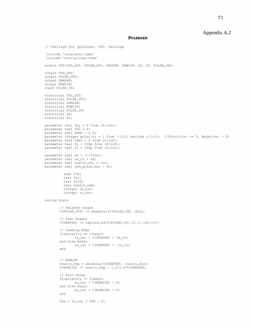
71
Appendix A.2 PULSEGEN
// VerilogA for jpLibTest, CFD, veriloga `include "constants.vams" `include "disciplines.vams" module CFD(CFD_OUT, PULSE_OUT, SHAPER, NOWLIN, LE, ZC, PULSE_IN); output CFD_OUT; output PULSE_OUT; output SHAPER; output NOWLIN; input PULSE_IN; electrical CFD_OUT; electrical PULSE_OUT; electrical SHAPER; electrical NOWLIN; electrical PULSE_IN; electrical LE; electrical ZC; parameter real dly = 0 from [0:inf); parameter real VDD = 5; parameter real AGND = 2.5; parameter integer polarity = 1 from [-1:1] exclude (-1:1); //(Positive: >= 0, Negative: < 0) parameter real tdel = 0 from [0:inf); parameter real tr = 100p from (0:inf); parameter real tf = 100p from (0:inf); parameter real w0 = 1/(750n); parameter real le_th = 1m; parameter real nowlin_dly = 16n; parameter real cfd_pulse_dly = 9n; real Vle; real Vzc; real Vcfd; real nowlin_tmp; integer le_out; integer zc_out; analog begin // Delayed output V(PULSE_OUT) <+ absdelay(V(PULSE_IN), dly); // Fast Shaper V(SHAPER) <+ laplace_nd(V(PULSE_IN),{0,1},{w0,1}); // Leading Edge if(polarity == 1)begin le_out = V(SHAPER) > le_th; end else begin le_out = V(SHAPER) < -le_th; end // NOWLIN nowlin_tmp = absdelay(V(SHAPER), nowlin_dly); V(NOWLIN) <+ nowlin_tmp - 1.0/2.0*V(SHAPER); // Zero Cross if(polarity == 1)begin zc_out = V(NOWLIN) > 0; end else begin zc_out = V(NOWLIN) < 0; end Vle = le_out ? VDD : 0;
72
Vzc = zc_out ? VDD : 0; Vcfd = (le_out && zc_out) ? VDD : 0; // Catch every thresshold cross @(cross(V(SHAPER) - (AGND + le_th), 0)); @(cross(V(NOWLIN), 0)); //@(timer(500u,1n)); @(cross(V(PULSE_OUT)-(AGND+polarity*10u),0)); // Leading Edge and Zero Cross outputs for debugging V(LE) <+ transition( Vle, tdel, tr, tf); V(ZC) <+ transition( Vzc, tdel, tr, tf); // CFD out V(CFD_OUT) <+ transition( Vcfd, tdel, tr, tf); end endmodule

73
APPENDIX B
PSD8C Pin Descriptions Pin number: 1 Pin name: acq_all Pin type: digital input Description: A positive going pulse will set the "hit" register in each of the
channels. This can be useful if one wants to force the acquisition of all channels on the chip.
Pin number: 2 Pin name: id1 Pin type: bi-directional Description: Bit 1 of the chip identification code. When "sel_ext_addr" is HIGH,
id1 is an input. Pin number: 3 Pin name: id3 Pin type: bi-directional Description: Bit 3 of the chip identification code. When "sel_ext_addr" is HIGH,
id3 is an input. Pin number: 4 Pin name: id5 Pin type: bi-directional Description: Bit 5 of the chip identification code. When "sel_ext_addr" is HIGH,
id5 is an input. Pin number: 5 Pin name: id7 Pin type: bi-directional Description: Bit 7 of the chip identification code. When "sel_ext_addr" is HIGH,
id5 is an input. Pin number: 6 Pin name: or_out Pin type: digital output Description: The "or_out" pin will be HIGH if any hit register on the chip is set. A
LOW on this pin indicates that NONE of the "hit" registers are set. Pin number: 7 Pin name: CFD_IN_6 Pin type: digital input Description: CFD input for channel 6 Pin number: 8 Pin name: CFD_IN_7 Pin type: digital input Description: CFD input for channel 7

74
Pin number: 9 Pin name: N/A Pin type: N/A Description: UNUSED (Will be used for CFD input if we expand to 16 channels.) Pin number: 10 Pin name: N/A Pin type: N/A Description: UNUSED (Will be used for CFD input if we expand to 16 channels.) Pin number: 11 Pin name: acq_clk Pin type: digital input Description: This is the clock signal used for acquisition. The rising edge of
"ack_clk" causes the active register to be set in a channel whose "hit" register is set AND whose "token_in" is active i.e. LOW. The falling edge of "acq_clk" in turn causes the "hit" register to be cleared. This in turn will potentially allow the "token_out" of the channel to be active i.e. LOW; thereby, enabling the next channel in the chain. The next rising edge of "acq_clk" will clear the active register.
Pin number: 12 Pin name: hit_sin Pin type: digital input Description: Serial input to the shadow register. Data on "hit_sin" pin must be
valid on rising edge of "hit_sclk". Pin number: 13 Pin name: hit_sclk Pin type: digital input Description: Serial clock for the shadow register. Data on "hit_sin" pin must be
valid on rising edge of "hit_sclk". Pin number: 14 Pin name: hit_transfer Pin type: digital input Description: Shadow register transfer signal. A rising edge on this pin will cause
the contents of the shadow register to be transferred into the hit register.
Pin number: 15 Pin name: event_en Pin type: digital input Description: This is externally generated timing signal. For triggering mode 1 and
2, timing is relative to the EventEn signal. For triggering mode 3, timing is relative to the CFDi signal.
75
Pin number: 16 Pin name: cfd_bypass Pin type: digital input Description: CFD bypass signal. This pin allows the CFD hit signals to be
bypassed, allowing the externally generated EventEn signal to determine the timing of the sub-channel integrators.
Pin number: 17 Pin name: common_stop Pin type: digital input Description: When HIGH, halts the time-to-voltage converter in every channel.
The time-to-voltage conversions will STOP even if the start conversion signal is still asserted.
Pin number: 18 Pin name: rst Pin type: digital input Description: Master reset. Resets all of the digital logic. All bits of the
configuration register are cleared. All of the DAC registers on chip are also cleared.
Pin number: 19 Pin name: CFD_IN_0 Pin type: digital input Description: CFD input for channel 0 Pin number: 20 Pin name: CFD_IN_1 Pin type: digital input Description: CFD input for channel 1 Pin number: 21 Pin name: N/A Pin type: N/A Description: UNUSED (Will be used for CFD input if we expand to 16 channels.) Pin number: 22 Pin name: N/A Pin type: N/A Description: UNUSED (Will be used for CFD input if we expand to 16 channels.) Pin number: 23 Pin name: DIG_LEFT_VDD Pin type: 5 Volt power pin Description: Connect to +5 volts. This pin supplies power only to the digital pads
on the left side of the chip.

76
Pin number: 24 Pin name: DIG_LEFT_GND Pin type: Ground pin Description: Connect to gnd. This pin supplies gnd only to the digital pads on the
left side of the chip. Pin number: 25 Pin name: TVC_CAP_GND_LEFT Pin type: analog Description: This is the return line for the capacitors in the TVC circuits on left
side of the chip (channels 0, 1, 6, and 7). Pin number: 26 Pin name: AGND_DELAY_GEN_LEFT Pin type: analog Description: This is the AGND signal that is used by the gate generators on left
side of the IC i.e. channels 0, 1, 6, and 7. Pin number: 27 Pin name: DLY_VC_CTL Pin type: analog Description: Control voltage that determines the time delay between a channel
being hit and the automatic reset of the time-to-voltage converter, integrators, and the active and hit registers in that channel. This signal is common to all channels on the IC.
Pin number: 28 Pin name: INTG_C_POS_OUT Pin type: analog Description: The C integrator outputs from the 8 channels are multiplexed to this
pin. The integrator output is brought off chip differentially. This is the (+) output.
Pin number: 29 Pin name: INTG_C_NEG_OUT Pin type: analog Description: The C integrator outputs from the 8 channels are multiplexed to this
pin. The integrator output is brought off chip differentially. This is the (-) output.
Pin number: 30 Pin name: TVC_POS_OUT Pin type: analog Description: The TVC outputs from the 8 channels are multiplexed to this pin.
The TVC output is brought off chip differentially. This is the (+) output.

77
Pin number: 31 Pin name: TVC_NEG_OUT Pin type: analog Description: The TVC outputs from the 8 channels are multiplexed to this pin.
The TVC output is brought off chip differentially. This is the (-) output.
Pin number: 32 Pin name: AVDD_PAD_LEFT Pin type: 5 Volt power pin Description: Connect to +5V. This pin supplies power to just the analog pads
located in lower left of pad frame. Pin number: 33 Pin name: AVSS_PAD_LEFT Pin type: Ground pin Description: Connect to gnd. This pin supplies gnd to just the analog pads located
in lower left of pad frame. Pin number: 34 Pin name: N/A Pin type: N/A Description: UNUSED Pin number: 35 Pin name: WA_CTL Pin type: analog Description: Control voltage for width of integration for the A integrators for all
channels on the chip. Pin number: 36 Pin name: WB_CTL Pin type: analog Description: Control voltage for width of integration for the B integrators for all
channels on the chip. Pin number: 37 Pin name: WC_CTL Pin type: analog Description: Control voltage for width of integration for the C integrators for all
channels on the chip. Pin number: 38 Pin name: AVDD_CH_LEFT_BOT Pin type: 5 Volt power pin Description: Connect to +5 Volt. This supplies power to channels 0 and 1.

78
Pin number: 39 Pin name: AVSS_CH_LEFT_BOT Pin type: Ground pin Description: Connect to gnd. This supplies gnd to channels 0 and 1. Pin number: 40 Pin name: AGND_CH_LEFT_BOT Pin type: analog Description: This is the AGND return line for the DACs in channel 0 and channel
1. There are 6 separate lines from sub-channels and they only connect at the pad. This was done to minimize cross-talk.
Pin number: 41 Pin name: CH_IN_0 Pin type: analog Description: Channel 0 detector input Pin number: 42 Pin name: CH_IN_1 Pin type: analog Description: Channel 1 detector input Pin number: 43 Pin name: N/A Pin type: N/A Description: UNUSED Pin number: 44 Pin name: N/A Pin type: N/A Description: UNUSED Pin number: 45 Pin name: TEMPERATURE Pin type: analog Description: This output can be used to infer die temperature. There is vertical
parasitic PNP transistor that is diode connected on the chip. The user should supply a temperature–independent (10 - 100 μA) constant current to this pin. The voltage at this pin may then be measured prior to applying power to the chip. The voltage will display a temperature coefficient of -2 mV/C. For example, if after some time the voltage on this pin decreased by 20 mV, then one could infer that the die was at a temperature of 10 degrees celsius above ambient.
Pin number: 46 Pin name: SUBSTRATE Pin type: analog Description: This is our connection to the top-side of the global substrate.
Connect the pin to gnd.

79
Pin number: 47 Pin name: MULTIPLICITY Pin type: analog Description: Analog output voltage proportional to the number of channels in
which the hit registers are set. Pin number: 48 Pin name: AGND_HI Pin type: analog Description: This is a high-impedance AGND line (no currents flow in it). Since the
output buffers have both an NFET and a PFET input stage, the stage NOT used (as determined by the polarity bit in the configuration register) has its inputs connected to this AGND pin.
Pin number: 49 Pin name: AVSS_COMMON Pin type: Ground pin Description: Connect to gnd. This pin supplies gnd to the analog circuits in the
“common” channel. Pin number: 50 Pin name: AVDD_COMMON Pin type: 5 Volt power pin Description: Connect to +5 Volts. This pin powers the analog circuits in the
“common” channel. Pin number: 51 Pin name: N/A Pin type: N/A Description: Currently unused. This pin is reserved for future expansion. Pin number: 52 Pin name: N/A Pin type: N/A Description: Current unused. This pin is reserved for future expansion. Pin number: 53 Pin name: CH_IN_2 Pin type: analog Description: Channel 2 detector input. Pin number: 54 Pin name: CH_IN_3 Pin type: analog Description: Channel 3 detector input.

80
Pin number: 55 Pin name: AGND_CH_RIGHT_BOT Pin type: analog Description: This is the AGND return line for the DACs in channel 2 and channel
3. There are 6 separate lines from the sub-channels and they only connect at this pad. This was done to minimize cross-talk.
Pin number: 56 Pin name: AVSS_CH_RIGHT_BOT Pin type: Ground pin Description: Connect to gnd. This supplies gnd to channels 2 and 3. Pin number: 57 Pin name: AVDD_CH_RIGHT_BOT Pin type: +5 Volt supply pin Description: Connect to +5 Volts. This supplies power to channels 2 and 3. Pin number: 58 Pin name: DC_CTL Pin type: analog Description: Control voltage for delay of subchannel C. For triggering mode 1 and
2, this is relative to the EventEn signal. For triggering mode 3, this is relative to the CFD hit signal.
Pin number: 59 Pin name: DB_CTL Pin type: analog Description: Control voltage for delay of subchannel B. For triggering mode 1 and
2, this is relative to the EventEn signal. For triggering mode 3, this is relative to the CFD hit signal.
Pin number: 60 Pin name: DA_CTL Pin type: analog Description: Control voltage for delay of subchannel A. For triggering mode 1 and
2, this is relative to the EventEn signal. For triggering mode 3, this is relative to the CFD hit signal.
Pin number: 61 Pin name: N/A Pin type: N/A Description: UNUSED Pin number: 62 Pin name: No pad. Pin type: No pad. Description: SUBSTRATE DOWNBOND. Connect to gnd.

81
Pin number: 63 Pin name: N/A Pin type: N/A Description: UNUSED Pin number: 64 Pin name: N/A Pin type: N/A Description: UNUSED Pin number: 65 Pin name: AVSS_PAD_RIGHT Pin type: Ground Pin Description: Connect to gnd. This pin supplies gnd to just the analog pads located
in lower right of pad frame. Pin number: 66 Pin name: AVDD_PAD_RIGHT Pin type: 5 Volt power pin Description: Connect to +5V. This pin supplies power to just the analog pads
located in lower right of pad frame. Pin number: 67 Pin name: INTG_A_POS_OUT Pin type: analog Description: The A integrator outputs from the 8 channels are multiplexed to this
pin. The integrator output is brought off chip differentially. This is the (+) output.
Pin number: 68 Pin name: INTG_A_NEG_OUT Pin type: analog Description: The A integrator outputs from the 8 channels are multiplexed to this
pin. The integrator output is brought off chip differentially. This is the (-) output.
Pin number: 69 Pin name: INTG_B_POS_OUT Pin type: analog Description: The B integrator outputs from the 8 channels are multiplexed to this
pin. The integrator output is brought off chip differentially. This is the (+) output.
Pin number: 70 Pin name: INTG_B_NEG_OUT Pin type: analog Description: The B integrator outputs from the 8 channels are multiplexed to this
pin. The integrator output is brought off chip differentially. This is the (-) output.

82
Pin number: 71 Pin name: AGND_DELAY_GEN_RIGHT Pin type: analog Description: This is the AGND signal that is used by the gate generators on right
side of the IC i.e. channels 2, 3, 4, and 5. Pin number: 72 Pin name: TVC_CAP_GND_RIGHT Pin type: analog Description: This is the return line for the capacitors in the TVC circuits on right
side of the chip (channels 2, 3, 4, and 5). Pin number: 73 Pin name: DIG_RIGHT_GND Pin type: Ground Pin Description: Connect to gnd. This is the gnd connection for the digital pads on the
right-side of the chip. Pin number: 74 Pin name: DIG_RIGHT_VDD Pin type: 5 Volt power pin Description: Connect to +5 Volts. This is the power connection for the digital pads
on the right-side of the chip Pin number: 75 Pin name: N/A Pin type: N/A Description: UNUSED Pin number: 76 Pin name: N/A Pin type: N/A Description: UNUSED Pin number: 77 Pin name: CFD_IN_2 Pin type: digital input Description: CFD input for channel 2 Pin number: 78 Pin name: CFD_IN_3 Pin type: digital input Description: CFD input for channel 3

83
Pin number: 79 Pin name: cfd_out Pin type: digital output Description: This is the output (for the selected channel) of the 100 ns one-shot
that is triggered by the narrow output pulse from the CFD. The CFD outputs from all 8 channels are multiplexed. This is the output of the multiplexer.
Pin number: 80 Pin name: intx_out Pin type: digital output Description: When test_mode_int (pin 128) is HIGH the integration region of the
channel/sub-channel currently selected is routed to this pin. The user should trigger their oscilloscope using either the EventEn or CFDi signal (applied to channel 1 of the scope) and then observe the intx_out signal on channel 2.
Pin number: 81 Pin name: force_rst Pin type: digital input Description: A positive going pulse on this line will reset the time-to-voltage and
integrators as well as the hit and active registers in ALL channels. Pin number: 82 Pin name: veto_rst Pin type: digital input Description: After a channel has been hit, the time-to-voltage and integrators as
well as the hit and active registers will automatically be reset UNLESS "veto_rst" is asserted (HIGH). The "veto_rst" signal must continue to be asserted until the time when the automatic reset would have taken place.
Pin number: 83 Pin name: hit_sout Pin type: digital output Description: Serial output of the shadow register. Pin number: 84 Pin name: N/A Pin type: N/A Description: UNUSED (Will be used for CFD input if we expand to 16 channels.) Pin number: 85 Pin name: N/A Pin type: N/A Description: UNUSED (Will be used for CFD input if we expand to 16 channels.) Pin number: 86 Pin name: CFD_IN_4 Pin type: digital input Description: CFD input for channel 4

84
Pin number: 87 Pin name: CFD_IN_5 Pin type: digital input Description: CFD input for channel 5 Pin number: 88 Pin name: dac_stb Pin type: digital input Description: Data on the address pins (a0-a5) are latched into an internal address
latch on the rising edge of dac_stb. When dac_stb is high, data on the ext_addr lines will alter the DAC output whose channel is selected by the address stored in the internal address latch. On the falling edge the data on the address pins will be latched into the DAC register. IMPORTANT NOTE: Data on address lines a0-a5 must be stable and valid on both rising and falling edge of "dac_stb".
Pin number: 89 Pin name: id6 Pin type: bidirectional Description: Bit 6 of the chip identification code. When "sel_ext_addr" is HIGH,
id6 is an input. Pin number: 90 Pin name: id4 Pin type: bidirectional Description: Bit 4 of the chip identification code. When "sel_ext_addr" is HIGH,
id4 is an input. Pin number: 91 Pin name: id2 Pin type: bidirectional Description: Bit 2 of the chip identification code. When "sel_ext_addr" is HIGH,
id2 is an input. Pin number: 92 Pin name: id0 Pin type: bidirectional Description: Bit 0 of the chip identification code. When "sel_ext_addr" is HIGH,
id0 is an input. Pin number: 93 Pin name: sin Pin type: digital input Description: Serial input to 48-bit configuration register. Data on "sin" pin must
be valid on rising edge of "sclk".

85
Pin number: 94 Pin name: sclk Pin type: digital input Description: Serial clock for 48-bit configuration register. Data on "sin" pin must
be valid on rising edge of "sclk". Pin number: 95 Pin name: sout Pin type: digital output Description: Serial output from 48-bit configuration register. Pin number: 96 Pin name: acq_ack Pin type: digital output Description: The "acq_ack" pin will be HIGH during the acquisition process and
will go LOW once all channels have been acquired. Pin number: 97 Pin name: N/A Pin type: N/A Description: UNUSED Pin number: 98 Pin name: N/A Pin type: N/A Description: UNUSED Pin number: 99 Pin name: N/A Pin type: N/A Description: UNUSED Pin number: 100 Pin name: AVDD_CH_RIGHT_TOP Pin type: +5 V supply pin Description: Connect to +5 Volts. This supplies power to channels 4 and 5. Pin number: 101 Pin name: AVSS_CH_RIGHT_TOP Pin type: Ground pin Description: Connect to gnd. This supplies gnd to channels 4 and 5. Pin number: 102 Pin name: AGND_CH_RIGHT_TOP Pin type: analog Description: This is the AGND return line for the DACs in channel 4 and channel
5. There are 6 separate lines from the sub-channels and they only connect at this pad. This was done to minimize cross-talk.

86
Pin number: 103 Pin name: N/A Pin type: analog Description: UNUSED (Will be used for a channel input if we expand to 16
channels.) Pin number: 104 Pin name: N/A Pin type: analog Description: UNUSED (Will be used for a channel input if we expand to 16
channels.) Pin number: 105 Pin name: CH_IN_4 Pin type: analog input Description: Channel 4 detector input Pin number: 106 Pin name: CH_IN_5 Pin type: analog input Description: Channel 5 detector input Pin number: 107 Pin name: DIG_COMMON_AVDD Pin type: +5 Volt power Description: Connect to +5 Volts. This pin is used to power all digital circuits in
the “common” channel. Pin number: 108 Pin name: DIG_COMMON_GND Pin type: Ground Description: Connect to gnd. This pin is used to supply gnd to all digital circuits
in the “common” channel. Pin number: 109 Pin name: token_out Pin type: digital output Description: This is the token out of the chip. It is active LOW. When the line is
high, an acquisition is in progress. Pin number: 110 Pin name: token_in Pin type: digital input Description: This is the token into the chip. It is active LOW.
87
Pin number: 111 Pin name: sel_ext_addr Pin type: digital input Description: When HIGH, this signal selects the external address as input to the
decoder used for selecting one of the 8 channels. When HIGH, makes a0-a4 lines as well as id0-id7 lines inputs.
Pin number: 112 Pin name: sc1 Pin type: digital input Description: This is external address line sc0. This is the most significant bit of
the address of the subchannel which the user wishes to select. Pin number: 113 Pin name: sc0 Pin type: digital input Description: This is external address line sc0. This is the least significant bit of
the address of the subchannel which the user wishes to select. Sub-channel address 00 selects the A integrator, 01 selects the B integrator, and 10 selects the C integrator. The code 11 is currently unused.
Pin number: 114 Pin name: a4 Pin type: bidirectional Description: This is external address line a4. See description for address line a0. Pin number: 115 Pin name: a3 Pin type: bidirectional Description: This is external address line a3. See description for address line a0. Pin number: 116 Pin name: a2 Pin type: bidirectional Description: This is external address line a2. See description for address line a0. Pin number: 117 Pin name: a1 Pin type: bidirectional Description: This is external address line a1. See description for address line a0. Pin number: 118 Pin name: a0 Pin type: bidirectional Description: This is external address line a0. When the "sel_ext_addr" pin is
HIGH, this line will be a DIGITAL INPUT and is the least significant bit of the address of the channel the user wishes to select. When the "sel_ext_addr" pin is LOW, this line will be a DIGITAL OUTPUT and will be the least significant bit of the address of the channel that is currently in need of attention.

88
Pin number: 119 Pin name: CH_IN_6 Pin type: analog input Description: Channel 6 detector input Pin number: 120 Pin name: CH_IN_7 Pin type: analog input Description: Channel 7 detector input Pin number: 121 Pin name: N/A Pin type: N/A Description: UNUSED. Pin number: 122 Pin name: N/A Pin type: N/A Description: UNUSED Pin number: 123 Pin name: AGND_CH_LEFT_TOP Pin type: analog Description: This is the AGND return line for the DACs in channel 6 and channel
7. There are 6 separate lines from the sub-channels and they only connect at this pad. This was done to minimize cross-talk.
Pin number: 124 Pin name: AVSS_CH_LEFT_TOP Pin type: Ground pin Description: Connect to gnd. This supplies gnd to channels 6 and 7. Pin number: 125 Pin name: AVDD_CH_LEFT_TOP Pin type: +5 Volt supply pin Description: Connect to +5 Volts. This supplies power to channels 6 and 7. Pin number: 126 Pin name: N/A Pin type: N/A Description: UNUSED Pin number: 127 Pin name: N/A Pin type: N/A Description: UNUSED

89
Pin number: 128 Pin name: test_mode_int Pin type: digital input Description: When test_mode_int (pin 128) is HIGH the integration region of the
channel/sub-channel currently selected is routed to this pin. The user should trigger their oscilloscope using either the EventEn or CFDi signal (applied to channel 1 of the scope) and then observe the intx_out signal on channel 2.

90
APPENDIX C
PSD8C Bonding Diagram