designing an efficient approach for jk and t flip-flop with power ...
Upload
nguyenkhuongCategory
view
214download
0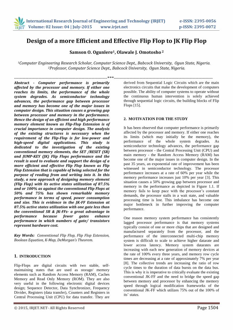
International Research Journal of Engineering and Technology (IRJET) e-ISSN: 2395-0056
Volume: 02 Issue: 04 | July-2015 www.irjet.net p-ISSN: 2395-0072
© 2015, IRJET.NET- All Rights Reserved Page 1504
Design of a more Efficient and Effective Flip Flop to JK Flip Flop
Samson O. Ogunlere1, Olawale J. Omotosho 2
1Computer Engineering Research Scholar, Computer Science Dept., Babcock University, Ogun State, Nigeria. 2Professor, Computer Science Dept., Babcock University, Ogun State, Nigeria.
-----------------------------------------------------------------***--------------------------------------------------------------------- Abstract - Computer performance is primarily affected by the processor and memory. If either one reaches its limits, the performance of the whole system degrades. As semiconductor technology advances, the performance gap between processor and memory has become one of the major issues in computer design. This situation causes a growing gap between processor and memory in the performance. Hence the design of an efficient and high performance memory element known as Flip-Flop Extension is of crucial importance in computer design. The analysis of the existing structures is necessary when the requirement of the Flip-Flop is for low-power and high-speed digital applications. This study is dedicated to the investigation of the existing conventional memory elements, the SET /RESET (SR) and JUMP-KEY (JK) Flip Flops performance and the result is used to evaluate and support the design of a more efficient and effective Flip Flop known as Flip Flop Extension that is capable of being selected for the purpose of reading from and writing into it. In this study, a new approach of designing memory element (Flip Flop) with its active states utilization of 87.5% and or 100% as against the conventional Flip Flops at 50% and 75% has shown remarkable memory performance in terms of speed, power consumption and size. This is evidence in the JK-FF Extension at 87.5% active states utilization with one gate less than the conventional SR & JK-FFs- a great advantage in performance because fewer gates enhance performance in which numbers of gate/ transistors represent hardware cost.
Key Words: Conventional Flip Flop, Flip Flop Extension, Boolean Equation, K-Map, DeMorgan’s Theorem.
1. INTRODUCTION
Flip-Flops are digital circuits with two stable, self-
maintaining states that are used as storage/ memory
elements such as Random Access Memory (RAM), Caches
Memory and Read Only Memory (ROM). They are also
very useful in the following electronic digital devices
design; Sequence Detector, Data Synchronizer, Frequency
Divider, Registers (data transfer), Counters and Registers in
Central Processing Unit (CPU) for data transfer. They are
derived from Sequential Logic Circuits which are the main
electronics circuits that make the development of computers
possible. The ability of computer systems to operate without
the continuous human intervention is solely achieved
through sequential logic circuits, the building blocks of Flip
Flops [15].
2. MOTIVATION FOR THE STUDY
It has been observed that computer performance is primarily
affected by the processor and memory. If either one reaches
its limits (which may initially be the memory), the
performance of the whole system degrades. As
semiconductor technology advances, the performance gap
between processor - the Central Processing Unit (CPU) and
main memory - the Random Access Memory (RAM) has
become one of the major issues in computer design. In the
past 35 years, an exponential rate of improvement has been
witnessed in semiconductor technology. The processor
performance increases at a rate of 60% per year while the
memory performance increases just 10% per year [3]. This
situation causes a 50% growing gap between processor and
memory in the performance as depicted in Figure 1.1. If
memory fails to keep pace with the processor’s constant
demands, the processor stalls in a wait state, and valuable
processing time is lost. This imbalance has become one
major bottleneck in further improving the computer
performance.
One reason memory system performance has consistently
lagged processor performance is that memory systems
typically consist of one or more chips that are designed and
manufactured separately from the processor, and the
performance of the interconnected multi-chip memory
system is difficult to scale to achieve higher datarate and
lower access latency. Memory system datarates are
increasing with each new generation of memory devices at
the rate of 100% every three years, and memory row cycle
times are decreasing at a rate of approximately 7% per year
[8]. The collective trends are increasing the ratio of row
cycle times to the duration of data bursts on the data bus.
This is why it is imperative to critically evaluate the existing
conventional JK-FF and the need to bridge the speed gap
between memory and processor by enhancing the memory
speed through logical modification frameworks of the
conventional JK-FF which utilizes 75% out of the 100% of
its’ states.
International Research Journal of Engineering and Technology (IRJET) e-ISSN: 2395-0056
Volume: 02 Issue: 04 | July-2015 www.irjet.net p-ISSN: 2395-0072
© 2015, IRJET.NET- All Rights Reserved Page 1505
Figure 1.1: Processor and DRAM Memory Gap showing
growing trend of increasing Processor Performance over
DRAM Performance over Time, (Inouye et al.., 2012)
3. DESIGNING SR AND JK-FLIP FLOPS
We start by designing JK-FF from first principle Set and
Reset Flip Flop (SR-FF) using NOR and NAND gate
Configurations. When the ‘forbidden states’ of an SR-Flip
Flop (as shown in Table 1.1) are converted to toggling
states, a JK-Flip Flop is so obtained. Hence, such a JK-Flip
Flop retains the rest features of an SR-Flip Flop, such as its
resting and active states; thus making a JK-Flip Flop to
attain 75% active states utilization as against 50% active
states utilization of an SR-Flip Flop on conversion of SR-FF
to JK-FF. The remaining 25% rest state of SR-FF is being
examined in this study.
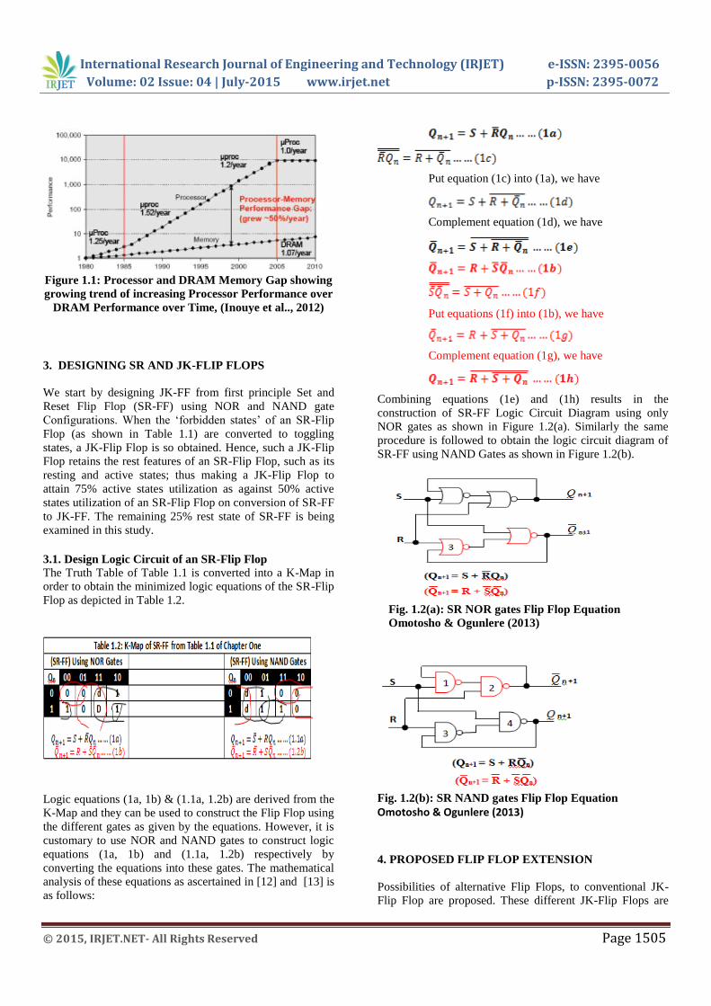
3.1. Design Logic Circuit of an SR-Flip Flop
The Truth Table of Table 1.1 is converted into a K-Map in
order to obtain the minimized logic equations of the SR-Flip
Flop as depicted in Table 1.2.
Logic equations (1a, 1b) & (1.1a, 1.2b) are derived from the
K-Map and they can be used to construct the Flip Flop using
the different gates as given by the equations. However, it is
customary to use NOR and NAND gates to construct logic
equations (1a, 1b) and (1.1a, 1.2b) respectively by
converting the equations into these gates. The mathematical
analysis of these equations as ascertained in [12] and [13] is
as follows:
Put equation (1c) into (1a), we have
Complement equation (1d), we have
Put equations (1f) into (1b), we have
Complement equation (1g), we have
Combining equations (1e) and (1h) results in the
construction of SR-FF Logic Circuit Diagram using only
NOR gates as shown in Figure 1.2(a). Similarly the same
procedure is followed to obtain the logic circuit diagram of
SR-FF using NAND Gates as shown in Figure 1.2(b).
Fig. 1.2(a): SR NOR gates Flip Flop Equation
Omotosho & Ogunlere (2013)
Fig. 1.2(b): SR NAND gates Flip Flop Equation
Omotosho & Ogunlere (2013)
4. PROPOSED FLIP FLOP EXTENSION
Possibilities of alternative Flip Flops, to conventional JK-
Flip Flop are proposed. These different JK-Flip Flops are
4
Q n +1
Q n+1
International Research Journal of Engineering and Technology (IRJET) e-ISSN: 2395-0056
Volume: 02 Issue: 04 | July-2015 www.irjet.net p-ISSN: 2395-0072
© 2015, IRJET.NET- All Rights Reserved Page 1506
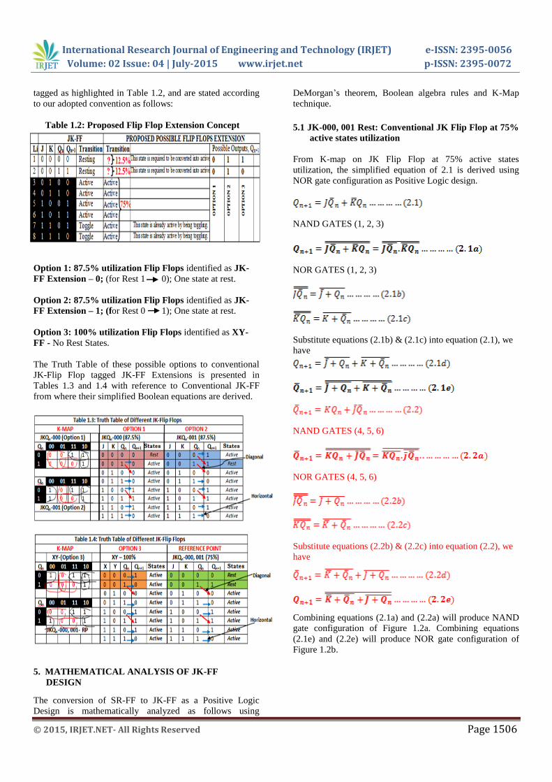
tagged as highlighted in Table 1.2, and are stated according
to our adopted convention as follows:
Table 1.2: Proposed Flip Flop Extension Concept
Option 1: 87.5% utilization Flip Flops identified as JK-
FF Extension – 0; (for Rest 1 0); One state at rest.
Option 2: 87.5% utilization Flip Flops identified as JK-
FF Extension – 1; (for Rest 0 1); One state at rest.
Option 3: 100% utilization Flip Flops identified as XY-
FF - No Rest States.
The Truth Table of these possible options to conventional
JK-Flip Flop tagged JK-FF Extensions is presented in
Tables 1.3 and 1.4 with reference to Conventional JK-FF
from where their simplified Boolean equations are derived.
5. MATHEMATICAL ANALYSIS OF JK-FF
DESIGN
The conversion of SR-FF to JK-FF as a Positive Logic
Design is mathematically analyzed as follows using
DeMorgan’s theorem, Boolean algebra rules and K-Map
technique.
5.1 JK-000, 001 Rest: Conventional JK Flip Flop at 75%
active states utilization
From K-map on JK Flip Flop at 75% active states
utilization, the simplified equation of 2.1 is derived using
NOR gate configuration as Positive Logic design.
NAND GATES (1, 2, 3)
NOR GATES (1, 2, 3)
Substitute equations (2.1b) & (2.1c) into equation (2.1), we
have
NAND GATES (4, 5, 6)
NOR GATES (4, 5, 6)
Substitute equations (2.2b) & (2.2c) into equation (2.2), we
have
Combining equations (2.1a) and (2.2a) will produce NAND
gate configuration of Figure 1.2a. Combining equations
(2.1e) and (2.2e) will produce NOR gate configuration of
Figure 1.2b.
International Research Journal of Engineering and Technology (IRJET) e-ISSN: 2395-0056
Volume: 02 Issue: 04 | July-2015 www.irjet.net p-ISSN: 2395-0072
© 2015, IRJET.NET- All Rights Reserved Page 1507
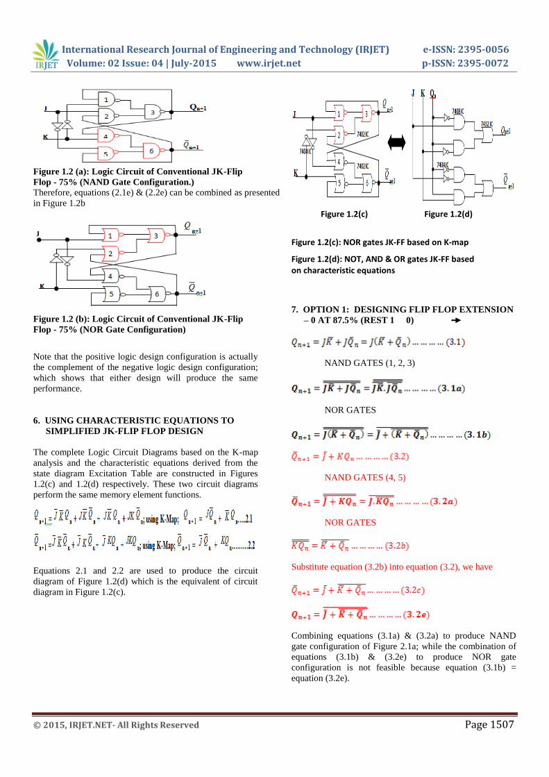
Figure 1.2 (a): Logic Circuit of Conventional JK-Flip
Flop - 75% (NAND Gate Configuration.)
Therefore, equations (2.1e) & (2.2e) can be combined as presented
in Figure 1.2b
Figure 1.2 (b): Logic Circuit of Conventional JK-Flip
Flop - 75% (NOR Gate Configuration)
Note that the positive logic design configuration is actually
the complement of the negative logic design configuration;
which shows that either design will produce the same
performance.
6. USING CHARACTERISTIC EQUATIONS TO
SIMPLIFIED JK-FLIP FLOP DESIGN
The complete Logic Circuit Diagrams based on the K-map
analysis and the characteristic equations derived from the
state diagram Excitation Table are constructed in Figures
1.2(c) and 1.2(d) respectively. These two circuit diagrams
perform the same memory element functions.
Equations 2.1 and 2.2 are used to produce the circuit
diagram of Figure 1.2(d) which is the equivalent of circuit
diagram in Figure 1.2(c).
Figure 1.2(c) Figure 1.2(d)
Figure 1.2(c): NOR gates JK-FF based on K-map
Figure 1.2(d): NOT, AND & OR gates JK-FF based on characteristic equations
7. OPTION 1: DESIGNING FLIP FLOP EXTENSION
– 0 AT 87.5% (REST 1 0)
NAND GATES (1, 2, 3)
NOR GATES
NAND GATES (4, 5)
NOR GATES
Substitute equation (3.2b) into equation (3.2), we have
Combining equations (3.1a) & (3.2a) to produce NAND
gate configuration of Figure 2.1a; while the combination of
equations (3.1b) & (3.2e) to produce NOR gate
configuration is not feasible because equation (3.1b) =
equation (3.2e).
International Research Journal of Engineering and Technology (IRJET) e-ISSN: 2395-0056
Volume: 02 Issue: 04 | July-2015 www.irjet.net p-ISSN: 2395-0072
© 2015, IRJET.NET- All Rights Reserved Page 1508
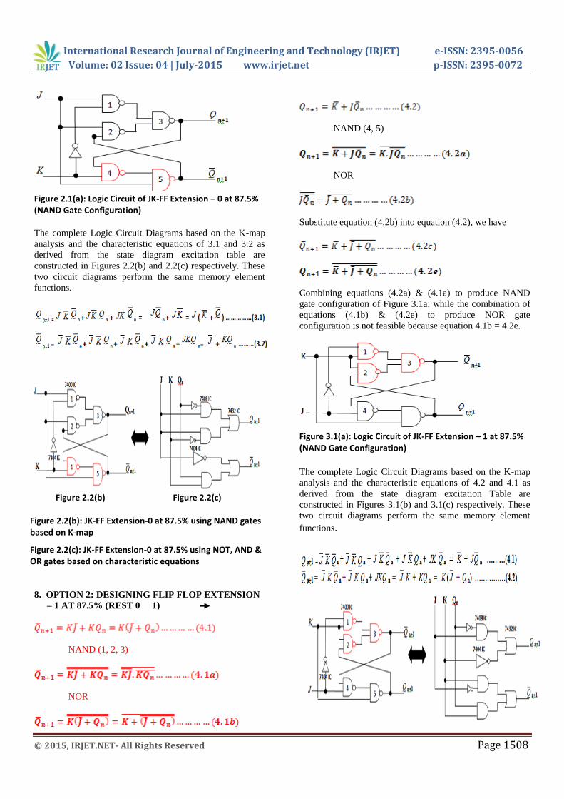
Figure 2.1(a): Logic Circuit of JK-FF Extension – 0 at 87.5% (NAND Gate Configuration) The complete Logic Circuit Diagrams based on the K-map
analysis and the characteristic equations of 3.1 and 3.2 as
derived from the state diagram excitation table are
constructed in Figures 2.2(b) and 2.2(c) respectively. These
two circuit diagrams perform the same memory element
functions.
Figure 2.2(b) Figure 2.2(c)
Figure 2.2(b): JK-FF Extension-0 at 87.5% using NAND gates based on K-map
Figure 2.2(c): JK-FF Extension-0 at 87.5% using NOT, AND & OR gates based on characteristic equations
8. OPTION 2: DESIGNING FLIP FLOP EXTENSION
– 1 AT 87.5% (REST 0 1)
NAND (1, 2, 3)
NOR
NAND (4, 5)
NOR
Substitute equation (4.2b) into equation (4.2), we have
Combining equations (4.2a) & (4.1a) to produce NAND
gate configuration of Figure 3.1a; while the combination of
equations (4.1b) & (4.2e) to produce NOR gate
configuration is not feasible because equation 4.1b = 4.2e.
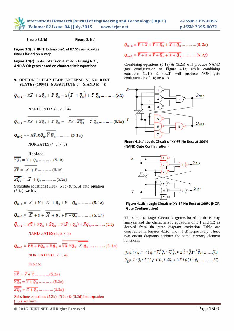
Figure 3.1(a): Logic Circuit of JK-FF Extension – 1 at 87.5% (NAND Gate Configuration)
The complete Logic Circuit Diagrams based on the K-map
analysis and the characteristic equations of 4.2 and 4.1 as
derived from the state diagram excitation Table are
constructed in Figures 3.1(b) and 3.1(c) respectively. These
two circuit diagrams perform the same memory element
functions.
International Research Journal of Engineering and Technology (IRJET) e-ISSN: 2395-0056
Volume: 02 Issue: 04 | July-2015 www.irjet.net p-ISSN: 2395-0072
© 2015, IRJET.NET- All Rights Reserved Page 1509
Figure 3.1(b) Figure 3.1(c)
Figure 3.1(b): JK-FF Extension-1 at 87.5% using gates NAND based on K-map
Figure 3.1(c): JK-FF Extension-1 at 87.5% using NOT, AND & OR gates based on characteristic equations
9. OPTION 3: FLIP FLOP EXTENSION; NO REST
STATES (100%)– SUBSTITUTE J = X AND K = Y
NAND GATES (1, 2, 3, 4)
NORGATES (4, 6, 7, 8)
Replace
Substitute equations (5.1b), (5.1c) & (5.1d) into equation
(5.1a), we have
NAND GATES (5, 6, 7, 8)
NOR GATES (1, 2, 3, 4)
Replace
Substitute equations (5.2b), (5.2c) & (5.2d) into equation
(5.2), we have
Combining equations (5.1a) & (5.2a) will produce NAND
gate configuration of Figure 4.1a; while combining
equations (5.1f) & (5.2f) will produce NOR gate
configuration of Figure 4.1b
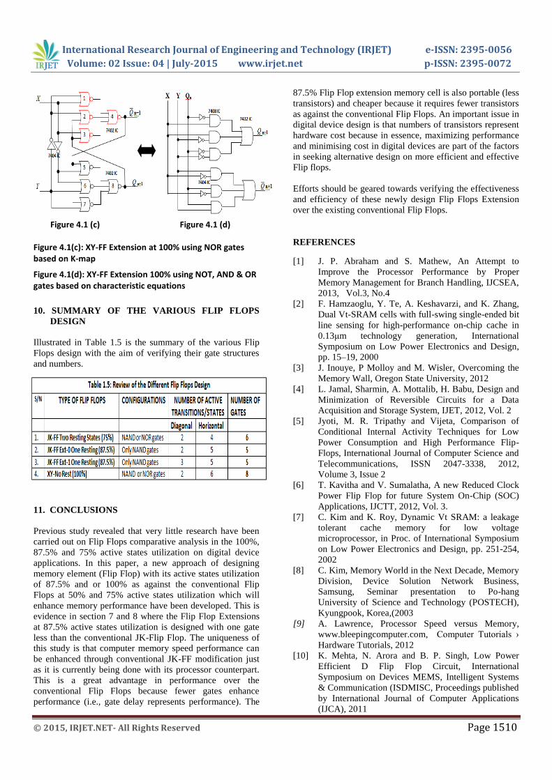
Figure 4.1(a): Logic Circuit of XY-FF No Rest at 100% (NAND Gate Configuration)
Figure 4.1(b): Logic Circuit of XY-FF No Rest at 100% (NOR Gate Configuration)
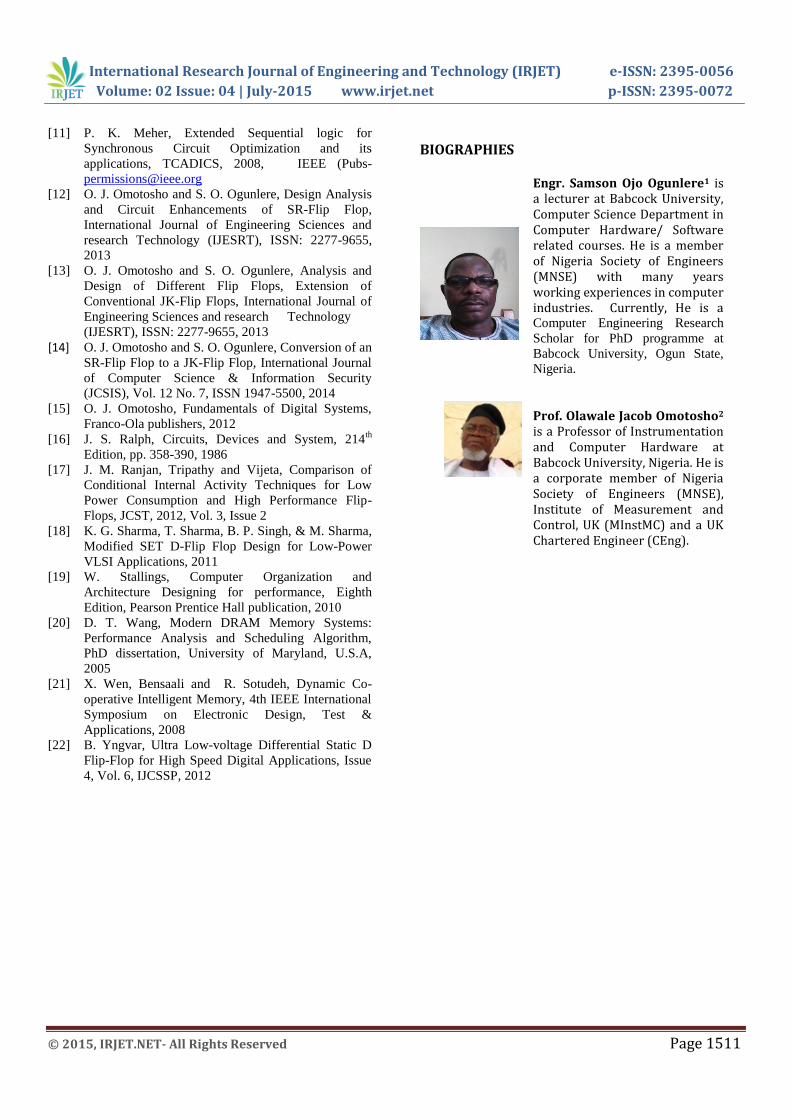
The complete Logic Circuit Diagrams based on the K-map
analysis and the characteristic equations of 5.1 and 5.2 as
derived from the state diagram excitation Table are
constructed in Figures 4.1(c) and 4.1(d) respectively. These
two circuit diagrams perform the same memory element
functions.
International Research Journal of Engineering and Technology (IRJET) e-ISSN: 2395-0056
Volume: 02 Issue: 04 | July-2015 www.irjet.net p-ISSN: 2395-0072
© 2015, IRJET.NET- All Rights Reserved Page 1510
Figure 4.1 (c) Figure 4.1 (d) Figure 4.1(c): XY-FF Extension at 100% using NOR gates based on K-map
Figure 4.1(d): XY-FF Extension 100% using NOT, AND & OR gates based on characteristic equations
10. SUMMARY OF THE VARIOUS FLIP FLOPS
DESIGN
Illustrated in Table 1.5 is the summary of the various Flip
Flops design with the aim of verifying their gate structures
and numbers.
11. CONCLUSIONS
Previous study revealed that very little research have been
carried out on Flip Flops comparative analysis in the 100%,
87.5% and 75% active states utilization on digital device
applications. In this paper, a new approach of designing
memory element (Flip Flop) with its active states utilization
of 87.5% and or 100% as against the conventional Flip
Flops at 50% and 75% active states utilization which will
enhance memory performance have been developed. This is
evidence in section 7 and 8 where the Flip Flop Extensions
at 87.5% active states utilization is designed with one gate
less than the conventional JK-Flip Flop. The uniqueness of
this study is that computer memory speed performance can
be enhanced through conventional JK-FF modification just
as it is currently being done with its processor counterpart.
This is a great advantage in performance over the
conventional Flip Flops because fewer gates enhance
performance (i.e., gate delay represents performance). The
87.5% Flip Flop extension memory cell is also portable (less
transistors) and cheaper because it requires fewer transistors
as against the conventional Flip Flops. An important issue in
digital device design is that numbers of transistors represent
hardware cost because in essence, maximizing performance
and minimising cost in digital devices are part of the factors
in seeking alternative design on more efficient and effective
Flip flops.
Efforts should be geared towards verifying the effectiveness
and efficiency of these newly design Flip Flops Extension
over the existing conventional Flip Flops.
REFERENCES
[1] J. P. Abraham and S. Mathew, An Attempt to
Improve the Processor Performance by Proper
Memory Management for Branch Handling, IJCSEA,
2013, Vol.3, No.4
[2] F. Hamzaoglu, Y. Te, A. Keshavarzi, and K. Zhang,
Dual Vt-SRAM cells with full-swing single-ended bit
line sensing for high-performance on-chip cache in
0.13μm technology generation, International
Symposium on Low Power Electronics and Design,
pp. 15–19, 2000
[3] J. Inouye, P Molloy and M. Wisler, Overcoming the
Memory Wall, Oregon State University, 2012
[4] L. Jamal, Sharmin, A. Mottalib, H. Babu, Design and
Minimization of Reversible Circuits for a Data
Acquisition and Storage System, IJET, 2012, Vol. 2
[5] Jyoti, M. R. Tripathy and Vijeta, Comparison of
Conditional Internal Activity Techniques for Low
Power Consumption and High Performance Flip-
Flops, International Journal of Computer Science and
Telecommunications, ISSN 2047-3338, 2012,
Volume 3, Issue 2
[6] T. Kavitha and V. Sumalatha, A new Reduced Clock
Power Flip Flop for future System On-Chip (SOC)
Applications, IJCTT, 2012, Vol. 3.
[7] C. Kim and K. Roy, Dynamic Vt SRAM: a leakage
tolerant cache memory for low voltage
microprocessor, in Proc. of International Symposium
on Low Power Electronics and Design, pp. 251-254,
2002
[8] C. Kim, Memory World in the Next Decade, Memory
Division, Device Solution Network Business,
Samsung, Seminar presentation to Po-hang
University of Science and Technology (POSTECH),
Kyungpook, Korea,(2003
[9] A. Lawrence, Processor Speed versus Memory,
www.bleepingcomputer.com, Computer Tutorials ›
Hardware Tutorials, 2012
[10] K. Mehta, N. Arora and B. P. Singh, Low Power
Efficient D Flip Flop Circuit, International
Symposium on Devices MEMS, Intelligent Systems
& Communication (ISDMISC, Proceedings published
by International Journal of Computer Applications
(IJCA), 2011
International Research Journal of Engineering and Technology (IRJET) e-ISSN: 2395-0056
Volume: 02 Issue: 04 | July-2015 www.irjet.net p-ISSN: 2395-0072
© 2015, IRJET.NET- All Rights Reserved Page 1511
[11] P. K. Meher, Extended Sequential logic for
Synchronous Circuit Optimization and its
applications, TCADICS, 2008, IEEE (Pubs-
[12] O. J. Omotosho and S. O. Ogunlere, Design Analysis
and Circuit Enhancements of SR-Flip Flop,
International Journal of Engineering Sciences and
research Technology (IJESRT), ISSN: 2277-9655,
2013
[13] O. J. Omotosho and S. O. Ogunlere, Analysis and
Design of Different Flip Flops, Extension of
Conventional JK-Flip Flops, International Journal of
Engineering Sciences and research Technology
(IJESRT), ISSN: 2277-9655, 2013
[14] O. J. Omotosho and S. O. Ogunlere, Conversion of an
SR-Flip Flop to a JK-Flip Flop, International Journal
of Computer Science & Information Security
(JCSIS), Vol. 12 No. 7, ISSN 1947-5500, 2014 [15] O. J. Omotosho, Fundamentals of Digital Systems,
Franco-Ola publishers, 2012
[16] J. S. Ralph, Circuits, Devices and System, 214th
Edition, pp. 358-390, 1986
[17] J. M. Ranjan, Tripathy and Vijeta, Comparison of
Conditional Internal Activity Techniques for Low
Power Consumption and High Performance Flip-
Flops, JCST, 2012, Vol. 3, Issue 2
[18] K. G. Sharma, T. Sharma, B. P. Singh, & M. Sharma,
Modified SET D-Flip Flop Design for Low-Power
VLSI Applications, 2011
[19] W. Stallings, Computer Organization and
Architecture Designing for performance, Eighth
Edition, Pearson Prentice Hall publication, 2010
[20] D. T. Wang, Modern DRAM Memory Systems:
Performance Analysis and Scheduling Algorithm,
PhD dissertation, University of Maryland, U.S.A,
2005
[21] X. Wen, Bensaali and R. Sotudeh, Dynamic Co-
operative Intelligent Memory, 4th IEEE International
Symposium on Electronic Design, Test &
Applications, 2008
[22] B. Yngvar, Ultra Low-voltage Differential Static D
Flip-Flop for High Speed Digital Applications, Issue
4, Vol. 6, IJCSSP, 2012
BIOGRAPHIES
Engr. Samson Ojo Ogunlere1 is a lecturer at Babcock University, Computer Science Department in Computer Hardware/ Software related courses. He is a member of Nigeria Society of Engineers (MNSE) with many years working experiences in computer industries. Currently, He is a Computer Engineering Research
Scholar for PhD programme at
Babcock University, Ogun State,
Nigeria.
Prof. Olawale Jacob Omotosho2 is a Professor of Instrumentation and Computer Hardware at Babcock University, Nigeria. He is a corporate member of Nigeria Society of Engineers (MNSE), Institute of Measurement and Control, UK (MInstMC) and a UK Chartered Engineer (CEng).