Design of a Linear FMCW Radar Synthesizer with … · • Theoretical study of phase noise in phase...
166
Master of Science in Electronics February 2012 Egil Eide, IET Harald Rosshaug, Kongsberg Seatex AS Submission date: Supervisor: Co-supervisor: Norwegian University of Science and Technology Department of Electronics and Telecommunications Design of a Linear FMCW Radar Synthesizer with Focus on Phase Noise Ruben Undheim
Transcript of Design of a Linear FMCW Radar Synthesizer with … · • Theoretical study of phase noise in phase...
Master of Science in ElectronicsFebruary 2012Egil Eide, IETHarald Rosshaug, Kongsberg Seatex AS
Submission date:Supervisor:Co-supervisor:
Norwegian University of Science and TechnologyDepartment of Electronics and Telecommunications
Design of a Linear FMCW RadarSynthesizer with Focus on Phase Noise
Ruben Undheim

i
Problem Description
Student: Ruben Undheim
Title: Design of a Linear FMCW Radar Synthesizer With Focus on Phase Noise
Text:Phase noise is the most important performance parameter in phase locked synthesiz-ers and local oscillators of communication equipment and radars. In this exercise, asynthesizer will be constructed which will be used in a range/bearing measurementsystem based on FMCW radar principles.
Tasks:
• Theoretical study of phase noise in phase locked loops
• Analysis of the importance of the phase noise for the performance of a FMCWbased range/bearing measurement system
• A survey of alternative topologies for the synthesizer of an FMCW-basedrange/bearing measurement system. Possible frequency bands are: 5.46 GHz- 5.64 GHz and 9.2 GHz - 9.3GHz
• Construction of synthesizer based on chosen topology
External supervisor: Harald Rosshaug, Kongsberg Seatex AS
Internal supervisor: Egil Eide


iii
Abstract
The linear FMCW radar has become more and more popular in recent years mainlydue to advances in digital signal processing and the good performance of the radar atclose ranges. What puts limits to the performance is mainly phase noise. Becausetransmission and reception happen simultaneously, the phase noise will limit themaximum power that should be used and hence also the ability to detect weaktargets. By ensuring during the design process that the phase noise is low, theradar’s performance will thus get better. This thesis describes the construction of aFMCW radar frequency synthesizer where the focus is mainly on phase noise. Thefunctionality of the circuit is shown to be successful, but there is more phase noisethan what is predicted. Several causes for this are discussed. Important backgroundtheory about radars, phase noise and phase-locked loops is presented and severalsimulations are performed in order to get a better understanding. The conclusionof the work is that it is not very hard to build a synthesizer, but in order to tweakthe phase noise performance to be as good as the linear theory tells it to be, carefulattention must be paid during all stages of the design.
iv
Preface
This thesis concludes my Master Degree in Electronics Engineering at the NorwegianUniversity of Science and Technology (NTNU). It was carried out during the Winterof 2011/2012 and submitted to NTNU, Trondheim February 20th, 2012. The focus ismainly on how a synthesizer for an FMCW radar can be built, what its performanceissues may be, and then getting a thoroughly understanding of phase noise, the PLLand radar systems in general. It involves general circuit design, RF circuit design,PCB layout, microcontroller programming, simulations, soldering, measurementsetc.
I would like to thank Kongsberg Seatex AS for letting me work there and for fundingthe project, and especially my supervisor, Harald Rosshaug, for the assistance I havereceived during the work with the thesis.
I would also like to thank Egil Eide at NTNU for the questions he has helped meclear out.
Trondheim, February 20th, 2012Ruben Undheim
Contents
1 Introduction 1
2 Radars 32.1 Pulse Radar . . . . . . . . . . . . . . . . . . . . . . . . . . . . . . . . 4
2.1.1 Pulse-Doppler signal processing . . . . . . . . . . . . . . . . . 72.2 CW Radar . . . . . . . . . . . . . . . . . . . . . . . . . . . . . . . . . 82.3 FMCW Radar . . . . . . . . . . . . . . . . . . . . . . . . . . . . . . . 8
2.3.1 Ambiguity . . . . . . . . . . . . . . . . . . . . . . . . . . . . . 122.3.2 Target ID . . . . . . . . . . . . . . . . . . . . . . . . . . . . . 13
2.4 Frequencies . . . . . . . . . . . . . . . . . . . . . . . . . . . . . . . . 14
3 Phase Noise 173.1 Internally Generated Noise . . . . . . . . . . . . . . . . . . . . . . . . 17
3.1.1 Thermal noise . . . . . . . . . . . . . . . . . . . . . . . . . . . 173.1.2 Flicker noise . . . . . . . . . . . . . . . . . . . . . . . . . . . . 18
3.2 External Noise . . . . . . . . . . . . . . . . . . . . . . . . . . . . . . 183.3 What is Phase Noise? . . . . . . . . . . . . . . . . . . . . . . . . . . . 193.4 Why Phase Noise? . . . . . . . . . . . . . . . . . . . . . . . . . . . . 24
3.4.1 Leeson’s equation . . . . . . . . . . . . . . . . . . . . . . . . . 243.4.2 LTV model . . . . . . . . . . . . . . . . . . . . . . . . . . . . 263.4.3 Nonlinear models . . . . . . . . . . . . . . . . . . . . . . . . . 28
3.5 Propagation in Devices . . . . . . . . . . . . . . . . . . . . . . . . . . 293.5.1 Mixers . . . . . . . . . . . . . . . . . . . . . . . . . . . . . . . 293.5.2 Frequency multipliers . . . . . . . . . . . . . . . . . . . . . . . 30
3.6 Measurement Techniques . . . . . . . . . . . . . . . . . . . . . . . . . 303.6.1 Down-conversion and filtering of carrier . . . . . . . . . . . . . 313.6.2 Quadrature method . . . . . . . . . . . . . . . . . . . . . . . . 313.6.3 Delay line discriminator . . . . . . . . . . . . . . . . . . . . . 32
3.7 Jitter . . . . . . . . . . . . . . . . . . . . . . . . . . . . . . . . . . . . 32
4 Phase Locked Loops 354.1 Phase Detectors . . . . . . . . . . . . . . . . . . . . . . . . . . . . . . 37
4.1.1 PFD . . . . . . . . . . . . . . . . . . . . . . . . . . . . . . . . 374.2 Filter . . . . . . . . . . . . . . . . . . . . . . . . . . . . . . . . . . . . 384.3 Full Transfer Function . . . . . . . . . . . . . . . . . . . . . . . . . . 404.4 Tracking . . . . . . . . . . . . . . . . . . . . . . . . . . . . . . . . . . 414.5 Phase Noise in Phase Locked Loops . . . . . . . . . . . . . . . . . . . 43
v
vi CONTENTS
5 Degradation Effects in FMCW Radars 455.1 Phase Noise . . . . . . . . . . . . . . . . . . . . . . . . . . . . . . . . 45
5.1.1 Contribution to the unaccuracy of the distance estimation . . 475.2 Linearity and Quantization of Sweep . . . . . . . . . . . . . . . . . . 48
6 Topology 536.1 Possible Solutions . . . . . . . . . . . . . . . . . . . . . . . . . . . . . 53
6.1.1 Open loop . . . . . . . . . . . . . . . . . . . . . . . . . . . . . 536.1.2 PLL with variable prescaler . . . . . . . . . . . . . . . . . . . 546.1.3 DDS as the reference oscillator for the PLL . . . . . . . . . . 556.1.4 DDS output mixed directly with fixed oscillator . . . . . . . . 60
6.2 Chosen Topology . . . . . . . . . . . . . . . . . . . . . . . . . . . . . 606.2.1 Phase noise predictions . . . . . . . . . . . . . . . . . . . . . . 636.2.2 Bode diagram . . . . . . . . . . . . . . . . . . . . . . . . . . . 65
7 Circuit Design 677.1 Components . . . . . . . . . . . . . . . . . . . . . . . . . . . . . . . . 67
7.1.1 VCO . . . . . . . . . . . . . . . . . . . . . . . . . . . . . . . . 677.1.2 DDS . . . . . . . . . . . . . . . . . . . . . . . . . . . . . . . . 687.1.3 Low-pass filter . . . . . . . . . . . . . . . . . . . . . . . . . . . 727.1.4 Microcontroller . . . . . . . . . . . . . . . . . . . . . . . . . . 727.1.5 Phase detector . . . . . . . . . . . . . . . . . . . . . . . . . . 747.1.6 Loop filter . . . . . . . . . . . . . . . . . . . . . . . . . . . . . 757.1.7 Frequency reference . . . . . . . . . . . . . . . . . . . . . . . . 777.1.8 Voltage regulator . . . . . . . . . . . . . . . . . . . . . . . . . 78
7.2 Schematic . . . . . . . . . . . . . . . . . . . . . . . . . . . . . . . . . 787.3 PCB . . . . . . . . . . . . . . . . . . . . . . . . . . . . . . . . . . . . 78
7.3.1 Finished design . . . . . . . . . . . . . . . . . . . . . . . . . . 817.4 Verification of Board . . . . . . . . . . . . . . . . . . . . . . . . . . . 85
8 Measurements 898.1 Equipment . . . . . . . . . . . . . . . . . . . . . . . . . . . . . . . . . 898.2 Procedure . . . . . . . . . . . . . . . . . . . . . . . . . . . . . . . . . 89
8.2.1 Phase Noise . . . . . . . . . . . . . . . . . . . . . . . . . . . . 898.2.2 Step Response . . . . . . . . . . . . . . . . . . . . . . . . . . . 918.2.3 Sweep . . . . . . . . . . . . . . . . . . . . . . . . . . . . . . . 91
9 Results 939.1 Phase Noise . . . . . . . . . . . . . . . . . . . . . . . . . . . . . . . . 949.2 Frequency Step . . . . . . . . . . . . . . . . . . . . . . . . . . . . . . 989.3 Sweep . . . . . . . . . . . . . . . . . . . . . . . . . . . . . . . . . . . 100
10 Discussion 10310.1 Frequency Step Measurements . . . . . . . . . . . . . . . . . . . . . . 10310.2 Phase Noise Measurements . . . . . . . . . . . . . . . . . . . . . . . . 10610.3 Frequency Sweep Measurements . . . . . . . . . . . . . . . . . . . . . 10910.4 Overall Design . . . . . . . . . . . . . . . . . . . . . . . . . . . . . . . 110
CONTENTS vii
11 Conclusion 11311.1 Future Work . . . . . . . . . . . . . . . . . . . . . . . . . . . . . . . . 113
A Source Code ATtiny2313 123A.1 ad9858control.h . . . . . . . . . . . . . . . . . . . . . . . . . . . . . . 123A.2 ad9858control.c . . . . . . . . . . . . . . . . . . . . . . . . . . . . . . 124A.3 main-fixedfrequency.c . . . . . . . . . . . . . . . . . . . . . . . . . . . 127A.4 main-switchfreq.c . . . . . . . . . . . . . . . . . . . . . . . . . . . . . 128A.5 main-sweeper.c . . . . . . . . . . . . . . . . . . . . . . . . . . . . . . 128A.6 main-symsweeper.c . . . . . . . . . . . . . . . . . . . . . . . . . . . . 129
B In-System Programming (ISP) of AVR 131
C Source Code Octave 133C.1 phasenoise-doall.m . . . . . . . . . . . . . . . . . . . . . . . . . . . . 133C.2 phasenoise1.m . . . . . . . . . . . . . . . . . . . . . . . . . . . . . . . 135C.3 phasenoise2.m . . . . . . . . . . . . . . . . . . . . . . . . . . . . . . . 137C.4 sweep.m . . . . . . . . . . . . . . . . . . . . . . . . . . . . . . . . . . 138C.5 tracking-step.m . . . . . . . . . . . . . . . . . . . . . . . . . . . . . . 139C.6 cancellation.m . . . . . . . . . . . . . . . . . . . . . . . . . . . . . . . 142
D Direct Digital Synthesis (DDS) 145
E Datasheets 147E.1 HMC510LP5 . . . . . . . . . . . . . . . . . . . . . . . . . . . . . . . 147E.2 HMC698LP5 . . . . . . . . . . . . . . . . . . . . . . . . . . . . . . . 149E.3 AD9858 . . . . . . . . . . . . . . . . . . . . . . . . . . . . . . . . . . 152E.4 VFTX210 . . . . . . . . . . . . . . . . . . . . . . . . . . . . . . . . . 155E.5 ATtiny2313 . . . . . . . . . . . . . . . . . . . . . . . . . . . . . . . . 156

viii CONTENTS
Glossary
AM: Amplitude Modulation
CW: Continuous Wave
DAC: Digital to Analogue Converter
DDS: Direct Digital Synthesis
DUT: Device Under Test
FFT: Fast Fourier Transform
FM: Frequency Modulation
FMCW: Frequency Modulated Continuous Wave
IF: Intermediate Frequency
ISF: Impulse Sensitivity Function
LO: Local Oscillator
LTV: Linear, Time-Variant
MCU: Microcontroller Unit
OCXO: Oven-Controlled Crystal Oscillator
PCB: Printed Circuit Board
PD: Phase Detector
PFD: Phase/Frequency Detector
PI: Proportional-Integral (A regulator)
PLL: Phase Locked Loop
PRF: Pulse Repetition Frequency
PRI: Pulse Repetition Interval
RBW: Resolution Bandwidth
RPC: Reflected Power Canceller
SFDR: Spurious-free Dynamic Range
SMA: SubMiniature version A (coaxial connector)
SSB: Single Sideband
STC: Sensitivity Time Control
TCXO: Temperature-Compensated Crystal Oscillator
VBW: Video Bandwidth
VCO: Voltage Controlled Oscillator

Chapter 1
Introduction
In recent years, there has been a growing interest in the linear FMCW radar [1]. Ithas some properties that are not seen with the traditional pulse radar or its variety,the pulse-Doppler radar - the main advantage being higher performance at closeranges. This is very useful for radio navigation systems that are used to navigatenear obstacles. A typical example is marine vessels. They are often relatively big,and the captain will often struggle to keep every part of the vessel under observationwhen navigating in narrow areas or in bad weather.
As in other fields of electronics and signal engineering, noise is an important issue.For the FMCW radar, the main worry is more specifically phase noise. This categoryof noise appears in all systems which employ oscillators. Because transmission andreception happen simultaneously in an FMCW radar, the phase noise will limit themaximum power that it makes sense to use and hence also the ability to detect weaktargets. The fascinating and disturbing thing with phase noise is that it is very hardto get rid of when it first has appeared. Therefore it is of high importance to ensurethat the oscillators in the circuit are stable and show good phase noise performanceat many offset frequencies. Phase noise is not only important in radar systems butalso in communication systems. It is the major contributor to undesired phenomenasuch as interchannel interference, leading to increased bit error rates. In radar- andcommunication technology, phase noise is regarded in the frequency domain, but inother fields, like digital design, it is regarded in the time domain where it is calledjitter. Even here it may be of critical importance.
The aim of the thesis is to get an understanding of radar systems, investigate howthey can be implemented and what put limits to their capability. Furthermore, afrequency synthesizer will be implemented which will be used in a linear FMCWradar in the frequency band of 9.2-9.3 GHz. It must provide a very clean sweepin this frequency range and therefore phase noise will be one main consideration.Different theories have appeared during the last decades which attempt to explainwhat phase noise is and how it appears [2, 3, 4]. There is still not complete agreementon these issues, and it therefore remains somewhat a mystery.
To be able to design a synthesizer for the FMCW radar, knowledge of many kindsof circuits and devices is required. Two circuits that are particularly much used
1

CHAPTER 1. INTRODUCTION
nowadays are the Phase-locked loop (PLL) and the Direct Digital Synthesizer (DDS).The PLL can be considered a linear control theory system when it is in lock, so thatthe analysis can be simplified. It consists of several important parts that need to bewell understood. The DDS on the other hand, is mostly a digital circuit connectedto the world with an on-chip DAC.
The following three chapters present radars, phase noise and phase-locked loops.Further Chapter 5 presents a discussion and some simulations of the degradationeffects that appear in FMCW radars. Chapter 6 discusses different topologies thatcan be used for the design, while Chapter 7 presents the actual design. The thesissums up with the measurement results of the radar synthesizer and a discussion.
2 Ruben Undheim

Chapter 2
Radars
Radars use radio waves to estimate the distance, bearing and velocity of something.Something can either be one target, multiple targets or all targets in view as forimaging radars.
There are two main-types - the pulse radar and the continuous wave (CW) radar.They both have their advantages. In the beginning of the days of radio technology,the CW radar was the only one that was successfully made. [5] A single oscillatorrunning at a constant frequency could be used to transmit a carrier and the reflectedsignal from a moving target would then result in a received Doppler shift1. Thiswould then be proportional to the velocity of the target. It was first discoveredaccidentally when big ships near receivers caused changes to the received signalfrom a distant transmitter. This was a bistatic2 radar, but later the concept wasemployed on purpose and the first real radar appeared. With this technology, it wasnot possible to measure the distance to the target, but moving targets could moreor less easily be detected.
Figure 2.1: How marine vessels can use radars. In this case a pulse radar.
Later, when the technology allowed it, the pulse radar was made. Its principle iseasy to understand, but at that time, it was not that easy to implement. It wasnecessary to transmit very short pulses of a clean radio signal, and then be completelysilent for a while in order to receive the echo. The development of the pulse radar
1This is a change in frequency ∆f = 2v/λ for targets moving with a relative speed v2Bistatic means that the transmitter and the receiver are at different locations as opposed to
the normal monostatic radar.
3

CHAPTER 2. RADARS
advanced rapidly when the magnetron was invented in 1940 [6]. Much of the majordevelopment happened during World War II, when the different countries realizedthe benefit of detecting airplanes. The pulse radar was able to measure the distanceto the targets where the CW radar failed. As time went on, and electronics becamemore advanced, good pulse radars were developed with very high performance andthe continuous wave radars were almost forgotten. With the arrival of the pulse-Doppler radar, it was possible to measure both range and velocity with one singleradar.
Radars can be used for two main applications, namely target detection and imaging.Imaging radars try to make an image of the observed area, and they take all echosinto consideration. A prime example of this is the Synthetic Aperture Radar. It ismainly used from space to make a mapping of the earth’s surface. A target detectionradar tries to find the location of a certain or several objects.
This chapter will first present the traditional pulse radar and then the simple CWDoppler radar before proceeding with the explanation of the FMCW radar whichthe rest of the text will be about.
2.1 Pulse Radar
t
Transmitted waveform
Received echos
Figure 2.2: Principle of basic pulse radar
The basic pulse radar is intuitive to understand. A pulse is transmitted at regularintervals and the received echoes of this pulse define the targets. When we say apulse, it is actually a sine-wave of very short duration, even though most texts forgetto mention and illustrate this. We see that in order to detect and decide the distanceto a target far away, the length between the pulses, T (also called PRI ), needs to belong enough. The pulse flies at the speed of light, and it has to go back and forth,so the minimum time between each pulse in order to have no ambiguous ranges3 isgiven by:
T =2Rmax
c(2.1)
3Ambiguous range means that a certain reading on the radar screen can be caused by targetsat two different distances quite far apart from each other.
4 Ruben Undheim

2.1. PULSE RADAR
Rmax is the maximum range of the radar. Note that in Figure 2.2, the length of τ isoveremphasized. In traditional pulse radars, τ is very much smaller than T .
The inverse of T is called the pulse repetition frequency (PRF).
PRF =1
T=
c
2Rmax
(2.2)
Another fact that can be observed is that the length of each pulse, τ , defines howclose targets can be to each other and still distinguish them as two separate targets,and not a big one. This is known as the resolution. It is important to remember thatthe accuracy of a system is something else than the resolution. The accuracy can begood even though the resolution is bad. The accuracy is mainly degraded by noise.However, the resolution normally influences negatively the way noise degrades theaccuracy. So indirectly, bad resolution often causes worse accuracy.
f
Figure 2.3: One pulse in frequency domain
In the frequency domain, a pulse of a sine wave at a certain frequency looks like asinc-function centered at that frequency. The width of the main-lobe of the sinc-function is defined by the length of the pulse. A longer pulse will have a narrowermain-lobe of the sinc-function in frequency domain and will therefore use less band-width. There is therefore a relationship between the bandwidth of the pulse and theresolution of the radar.
xr =c
2B(2.3)
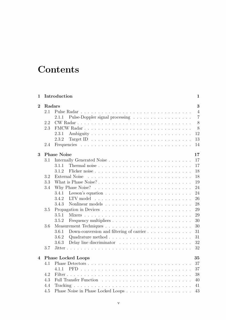
The spectrum with a single sinc-function is just applicable for the ideal case whenonly one single pulse is sent. However, when many pulses are sent after each other atregular intervals, the frequency specter will consist of many discrete lines which havean envelope of the sinc-function of the single-pulse case (Figure 2.4). The distancebetween these discrete lines is given by the PRF. The higher the PRF, the longerdistance between every discrete line. More advanced pulse radars, called pulse-Doppler Radars, take advantage of the frequency spacing between these discretelines in order to measure the Doppler shift of the returned pulses. The Doppler shiftappears when the target moves relatively to the radar. It is therefore an indicator ofvelocity. A moving target will shift the entire spectrum either up or down (depending
Design of a Linear FMCW Radar Synthesizer 5
CHAPTER 2. RADARS
on whether the target is approaching or not) and the velocity will be measured. Inorder to measure the velocity it is very important that the radar signal is coherent.That basically means that only the amplifier is turned off between the pulses and notthe oscillator. This is hard to do with a magnetron but easy to do with a klystronamplifier. Since the PRF defines the distance between the discrete lines, it willalso define how fast targets can be detected without getting an ambiguous velocityreading.
f
Figure 2.4: Many pulses in frequency domain
We therefore have a dilemma, increasing the PRF, improves the velocity ambiguities,while decreasing the PRF, improves the range ambiguities. Because the Doppler shiftgets higher if higher carrier frequencies are used, the problem also becomes bigger athigher frequencies. The pulse-Doppler Radar actually often ignores what was saidabove about that the distance between the pulses must be long enough to achieve noambiguous range. It makes a compromise between ambiguous range and ambiguousvelocity.
There are three different main-types of the pulse-Doppler Radar depending on howhigh the PRF is [7].
Low PRF: The PRF is kept so low that there will be no range ambiguities butmany velocity ambiguities.
Medium PRF: The PRF is kept higher so that there will be both range ambiguitiesand velocity ambiguities, but not so many of each.
High PRF: The PRF is kept so high that there will be no velocity ambiguities.However, there will be many range ambiguities.
The exact values of the PRFs for the different types above, depend on over whichregion in range and velocity the radar is supposed to operate.
Many methods have been made to cope with this problem of ambiguities. Onesolution is to use a variable PRF, often called staggering. It is quite commonlyused for high PRF-radars and will solve out the range ambiguities since they will bedifferent for the different PRFs that are used. Normally, at least 3 different PRFsare needed in order to solve all the ambiguities.
6 Ruben Undheim

2.1. PULSE RADAR
t
1 2 3 4 5 6 7 8 9 101112131415 1 2 3 4 5 6 7 8 9 101112131415
10
9
8
7
6
5
4
3
2
1
N
Quiescent phase Quiescent phase
N-FFTN-FFT N-FFT N-FFT
15 N-FFTs are performed
TX pulses
Figure 2.5: How Pulse-Doppler signal processing can be performed
2.1.1 Pulse-Doppler signal processing
Pulse-Doppler signal processing is nowadays used for most pulse radars. Here followsa short explanation of how it can be performed [8]. After the radar pulse has beenemitted, the receiver monitors the received echoes. The received signal during thetime between the pulses is called the quiescent phase. This time is divided intoM equally long bins corresponding to the desired range resolution - often calledrange gating in the literature. The received signal is mixed down to an intermediatefrequency with a local oscillator whose frequency is derived from the transmittedsignal. Following some filters at the IF frequency, the signal is mixed down inquadrature to baseband. One complex sample is thereby taken for each bin andsaved in a matrix in memory (see Figure 2.5). All the complex samples for thesucceeding bins are saved in the same row in the matrix. When then the next pulseis emitted, the following samples are saved in a new row. After N pulses a full matrixof M × N complex values are found. An N-FFT is taken for each column in thematrix. The result is multiple Doppler spectra. Each of them correspond to a timebin after one pulse and hence one ambiguous range. If a high PRF is used, each bincorresponds to several distances. The Doppler spectra will reveal the speed of themoving targets in each bin. Before the advent of FFT processors, the processing wasperformed with analogue filters and the structure was therefore slightly different.
Design of a Linear FMCW Radar Synthesizer 7
CHAPTER 2. RADARS
2.2 CW Radar
The CW radar uses a single oscillator running at a constant frequency. By takingadvantage of the Doppler shift, moving targets can be detected. The received signalis mixed with the transmitted signal and the beat signal4 will contain the Dopplershifts of the targets. The processing is much simpler than for the pulse-Dopplerprocessing. An FFT can be performed continuosly for the received signal. Themain problem is however that since the signal is stationary at a single frequency, thedistance to targets can not be found. The radar has been used, and is still used inmany different applications. A prime example is the police speed radar. Since therange is not interesting in this case, the basic CW radar does its job well.
One difficulty with the CW radar compared to the pulse radar is that it is receivingat the same time as it is transmitting. This will cause some of the transmitted signalto propagate or leak directly to the receiver. This is certainly the case if the sameantenna is used. Two different antennas (quasi-bistatic) are often used but still inthis case the leakage of the transmitted signal can be severe. As we will see, thisproblem is actually the biggest disadvantage of the CW radar, and its relative, theFMCW radar, which will be presented now.
2.3 FMCW Radar
The main problem of the CW radar above is that it is unable to measure the distanceto the target. In many cases this is exactly what we want. To be able to determinethe distance, the signal cannot be stationary. It must change somehow. It is possibleto either change the amplitude or the frequency. When the signal then returns fromthe target the distance can be calculated since it is known how the transmittedsignal looks like at all times. Changes of the amplitude are indeed very hard tomeasure because they are easily overloaded by the transmitted signal, and there isno way to filter out the returned signal. In addition, the amplitude of the returnedsignal is very variable depending on the exact angle in which the wave hits the targetand so on. There are few implementations of an amplitude modulated CW radar.An example is found in [9]. On the contrary, changing the frequency of the carrierhas proved to be a successfull thing to do. By frequency modulating the signal,the returned signal can more easily be filtered from the transmitted signal and thevariations depending on the illumination angle are much lower. This principle iscalled Frequency Modulated Continuous Wave Radar (FMCW). There have beenattempts to modulate the carrier with different wave forms. The first used wereprobably sine waves because of its simple implementation. Now, the most popularform is a linear sweep. This kind of radar is referred to as a linear FMCW radar.
The sweep may be from lower to higher frequencies, from higher to lower frequenciesor do both successively. The first two are referred to as asymmetrical linear FMCW
4The beat signal is the transmitted signal mixed with the received signal. Also called theconversion product.
8 Ruben Undheim

2.3. FMCW RADAR
Frequency
Time
Figure 2.6: How an asymmetrical linear sweep FMCW radar sweeps
radars (Figure 2.6), while the third is called a symmetrical linear FMCW radar(Figure 2.7). It has been discovered that the linear waveform has many advantagescompared to other waveforms [1]. The most obvious thing is probably that duringthe sweep, if the transmitted signal is mixed with the received signal, the beat signalwill be a signal containing a wave with a frequency that is exactly proportional tothe distance to the target. In Figure 2.6 and 2.7 the received signal is also indicatedin green. It should be noticed that the frequency of the received signal differs fromthe transmitted signal at a certain time instant.
Frequency
Time
Figure 2.7: How a symmetrical linear sweep FMCW radar sweeps
Let us do an analysis of a single sweep - here an up-sweep. If the instantaneousfrequency is given by [1]
ft = f0 + αt
where α is the sweep rate, the phase is:
φ = 2π
∫ t
0
ftdt = 2π
(
f0t+αt2
2
)
The transmitted signal can then written
s(t) = A0 sin 2π
(
f0t+αt2
2
)
(2.4)
If the signal is delayed by τ from the target, the received signal is:
sreceived(t) = B0 sin 2π
[
f0(t− τ) +α(t− τ)2
2
]
(2.5)
Design of a Linear FMCW Radar Synthesizer 9

CHAPTER 2. RADARS
Where B0 represents the loss in energy. Because of
2 sinx sin y = cos(x− y)− cos(x+ y)
the beat signal is:
c(t) = C0 cos 2π
[
f0τ + αtτ − ατ 2
2
]
(2.6)
Here the second component at twice the transmission frequency has been removed(filtered). The delay τ is
τ =2r
c
and therefore the beat signal can be written:
c(t) = C0 cos 2π
[
2f0r
c+
2αtr
c− α(2r/c)2
2
]
(2.7)
The only time-varying term is the middle one, 2αtr/c (for a non-moving target),and thus the only term leading to oscillation. The main frequency component of thebeat signal will hence be
fconversion =2αr
c(2.8)
Compared to the pulse radar, the FMCW radar has a number of advantages and itis almost surprising that it has not been used more before. Since the FMCW radartransmits continuously, the average power (energy) will be the same as the maximumpower. The pulse radar, on the other hand, outputs all its energy in a very shorttime period, so its average power will be low. The ability to detect targets is relatedto the average power, so in order to have the same detection ability, the pulse radarneeds a very high maximum power. It requires typically expensive amplifiers likeklystron amplifiers. An FMCW radar can use solid-state amplifiers which today aremuch cheaper to produce and can be highly integrated into the design of the radar.The low maximum power provides an advantage in another way too. It is harder todetect - the radar has a low probability of interception. For military use, this is veryvaluable, because it makes it harder for the enemy to manipulate the radar signal.
These are not the only advantages. Since the radar is receiving at all times, it doesnot have to wait for the pulse to be transmitted before it starts analyzing the receivedsignal. This causes a remarkable improvement of the minimum distance that canbe measured [10]. Furthermore, the range resolution is no longer dependent on howshort the pulse can be made, but on the total frequency sweep range that is employed.Since the processing then does not have to sample a very short pulse which requiresa high sample rate, its range resolution can easily be made considerably better.
The main issue, however, is the leakage from the transmitter to the receiver thatappears from the fact that it is receiving at the same time as it is transmitting. Itputs an upper limit to how strong the transmitted signal can be, and therefore also
10 Ruben Undheim
2.3. FMCW RADAR
the maximum range. Apart from this thing, it seems like the FMCW radar almosthas only advantages. It is implied that the digital revolution has happened and thatthe more complicated processing power needed can be satisfied. First of all thisconcerns an efficient FFT processor, but perhaps also the DDS.
One can conclude that the FMCW radar is very good for detection at near ranges,and the industry has started to discover this by now using it in several commercialproducts. Some examples are collision detection radars for cars, altitude measure-ment and near obstacle ship navigation.
Modulator Transmitter
×Receiver
Delay
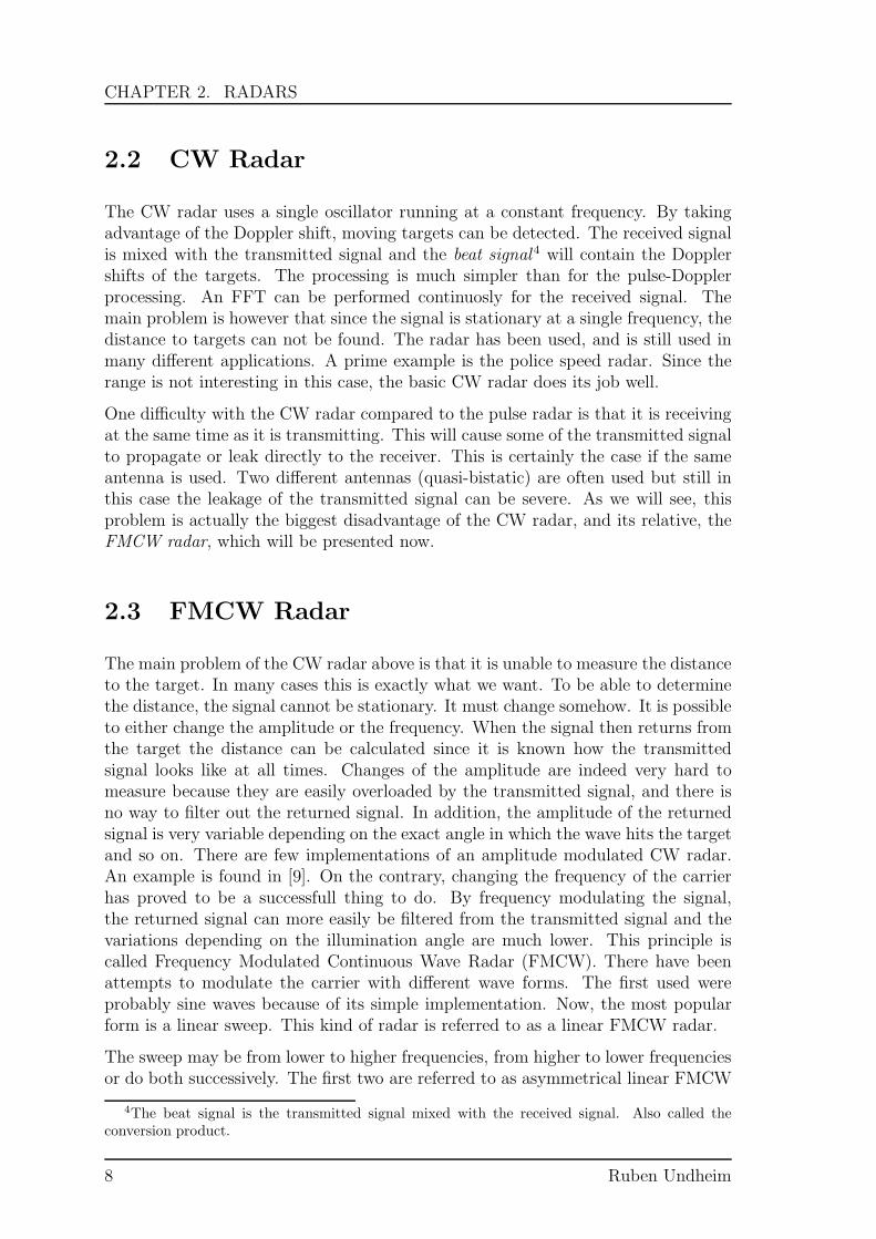
Figure 2.8: Conceptual diagram of an FMCW Radar. The transmitter leakage isindicated with the red line
Figure 2.8 is a simple diagram showing how an FMCW radar may be implemented.The modulator generates a sweep, which is transmitted by the transmitter. Thesame signal is taken to the receiver in order to mix with the reflected signal. Ahomodyne configuration is used. This means that the signal is mixed directly tobaseband (not via an intermediate frequency). The leakage from the transmitter tothe receiver is also illustrated in red. In the receiver, there can be an FFT processorwhich calculates the frequency spectrum of the beat signal. It is of course alsopossible to use a collection of filters. The receiver is in fact quite the same as for anormal CW radar.
The beat signal is sampled during the sweep. One FFT is normally calculated foreach sweep. The number of samples taken during one sweep therefore decides howbig the FFT must be. The sample rate defines the maximum beat signal frequencythat can be detected. By increasing the sample rate, the FFT must be made bigger,but that will only make it able to represent higher frequencies. Its resolution willnot get any better. If the sweep time is increased and the swept bandwidth iskept constant, the frequency sweep rate will decrease. Such a decrease causes thefrequency in the beat signal to be lower. The resolution will not get any better inthis case either. The only way to improve the resolution is therefore to increase thespan of the sweep and it can be shown that the resolution is given by (2.3) for theFMCW radar too.
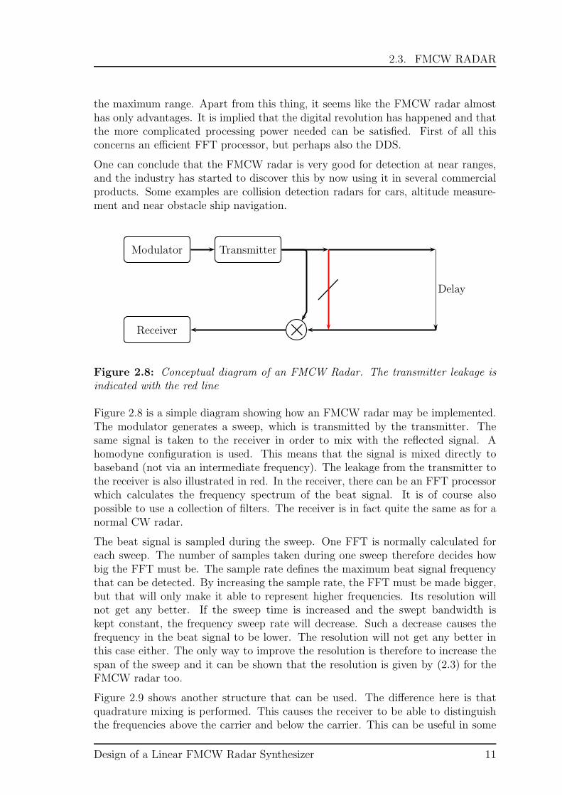
Figure 2.9 shows another structure that can be used. The difference here is thatquadrature mixing is performed. This causes the receiver to be able to distinguishthe frequencies above the carrier and below the carrier. This can be useful in some
Design of a Linear FMCW Radar Synthesizer 11
CHAPTER 2. RADARS
Modulator Transmitter
90
××
Receiver
Delay
I
Q
Figure 2.9: Conceptual diagram of FMCW Radar with complex processing
radar systems when for example the targets have IDs which are modulated ontothe carrier. In order to do the quadrature mixing, the transmitted signal must besplitted in two and one of the signals must be phase-shifted 90.
2.3.1 Ambiguity
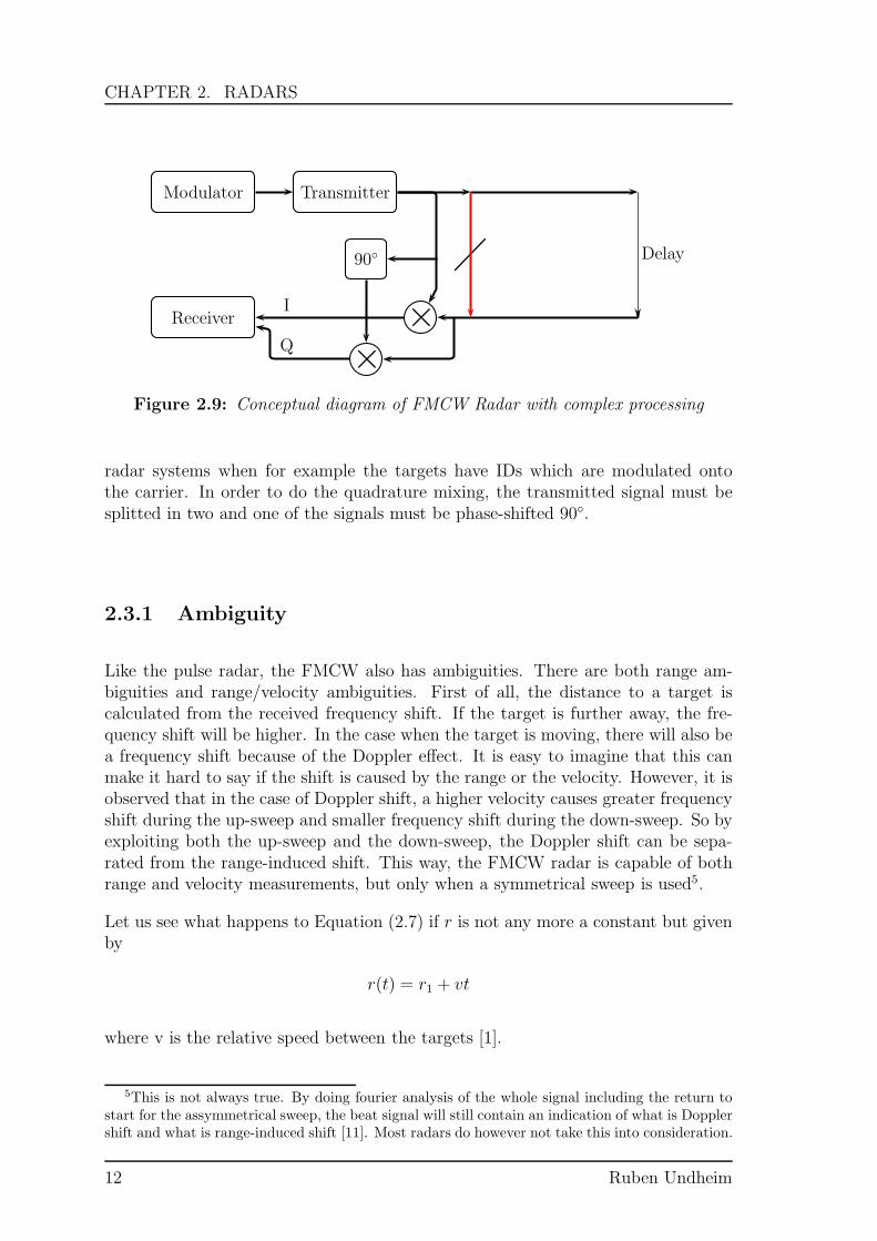
Like the pulse radar, the FMCW also has ambiguities. There are both range am-biguities and range/velocity ambiguities. First of all, the distance to a target iscalculated from the received frequency shift. If the target is further away, the fre-quency shift will be higher. In the case when the target is moving, there will also bea frequency shift because of the Doppler effect. It is easy to imagine that this canmake it hard to say if the shift is caused by the range or the velocity. However, it isobserved that in the case of Doppler shift, a higher velocity causes greater frequencyshift during the up-sweep and smaller frequency shift during the down-sweep. So byexploiting both the up-sweep and the down-sweep, the Doppler shift can be sepa-rated from the range-induced shift. This way, the FMCW radar is capable of bothrange and velocity measurements, but only when a symmetrical sweep is used5.
Let us see what happens to Equation (2.7) if r is not any more a constant but givenby
r(t) = r1 + vt
where v is the relative speed between the targets [1].
5This is not always true. By doing fourier analysis of the whole signal including the return tostart for the assymmetrical sweep, the beat signal will still contain an indication of what is Dopplershift and what is range-induced shift [11]. Most radars do however not take this into consideration.
12 Ruben Undheim

2.3. FMCW RADAR
c(t) = C0 cos 2π
[
f0 · 2(r1 + vt)
c+
αt · 2(r1 + vt)
c− α(2(r1 + vt)/c)2
2
]
(2.9)
= C0 cos 2π
[
2f0r1c
+2f0vt
c+
2αtr1c
+2αvt2
c− 2αr21
c2− 4αr1vt
c2− 2αv2t2
c2
]
= C0 cos 2π
[
2αr1t
c
(
1− 2v
c
)
+2f0vt
c+
2αvt2
c
(
1− v
c
)
+2r1c
(
f0 −αr1c
)
]
Thus, the contribution from the range and the velocity can now be seperated. Thefirst term belongs to the range and the second to the velocity:
fdue to range =2αr1c
(
1− 2v
c
)
(2.10)
fdue to velocity =2f0v
c= Doppler effect (2.11)
The third term:2αvt2
c
(
1− v
c
)
is also affected by the change of distance. As [1] states: It may either be interpretedas chirp on the range beat, due to the changing rate, or as chirp on the Doppler, dueto the changing transmitter frequency. The last term in (2.9) is a constant phaseterm and will hence not influence the frequency of the beat signal.
One thing that should be noted is that the frequency offset due to the range (2.10)is no longer equal (2.8). A factor (1− 2v/c) is added. It will of course not affect theresult much as long as the velocity is much lower than the speed of light.
Now let us take a look at the range ambiguities. In the extreme case, the sweepmay be so fast, or the target so far away, that when the reflected signal eventuallyreturns, the radar has already started on a new sweep. The returned signal can thenbe mistaken for being very much closer than it really is. For most practical purposesthis is however not the problem. The implementation of the sampling plays a biggerrole. Because the further away the target is, the higher the frequency shift will be,the sampling frequency sets the upper limit of the range, and according to Nyquistthis is Fs/2. If the low-pass filter in front of the AD converter is not good enough,there will be aliasing and targets further away than the maximum Nyquist rangecan be mistaken for being nearer.
2.3.2 Target ID
The returned signal from non-moving targets will as we have seen be a frequencyshifted ∆f = 2αr/c Hz. If there are many visible targets, it might be hard todistinguish the desired targets. When only a certain set of known targets are tobe tracked, it is possible to equip them with onboard oscillators and mixers so thatthe returned signal will be shifted in frequency. This makes it possible to easier
Design of a Linear FMCW Radar Synthesizer 13

CHAPTER 2. RADARS
recognize the known targets. Each of them may also be identified if different mixingfrequencies are used. The returned signal will contain two carriers, one on both sidesof the original returned signal at a frequency offset equal to the local oscillator ofthe targets. If the radar signal is given by:
s0(t) = sin 2π
(
f0t+1
2αt2)
And the local oscillator at a target j is given by:
sj(t) = sin(2πfjt)
The returned signal will be:
s(t) = s0(t) · sj(t) (2.12)
= sin 2π
(
f0(t− τ)− 1
2α(t− τ)2
)
· sin(2πfjt) (2.13)
=1
2cos 2π
(
(f0 − fj)t− f0τ +1
2α(t− τ)2
)
− 1
2cos 2π
(
(f0 + fj)t− f0τ +1
2α(t− τ)2
)
(2.14)
Thus, two carriers shifted with a frequency fj.
One other advantage of having such an oscillator at the targets, is that the returnedsignal will be shifted away from the worst phase noise of the transmitted signal.Hence, the sensitivity can be made better. Letting the targets have such an ID isone additonal thing that makes the FMCW radar attractive compared to a pulseradar.
2.4 Frequencies
For radars, a general rule is that the range resolution obtained is given by the band-width used by the transmitted signal. This attracts the use of high frequencies,because at these frequencies, a high bandwidth is not high proportional to the op-erating frequency, and the components of the radar won’t show big variations overthe band. Furthermore, there are more available bands at higher frequencies. Athird reason is that the waves do not propagate further than the horizon at thesefrequencies but more in a straight line. At last, the resolution in bearing can bemade better.
There are reasons for using lower frequencies too. First of all, the components usedat low frequencies are cheaper and easier to produce. Secondly, the higher frequencyused, the greater the Doppler shift will be and the sampling in Doppler domainneeds to be higher which implies a higher pulse repetition frequency (PRF) in the
14 Ruben Undheim

2.4. FREQUENCIES
case of a pulse radar. This reduces the maximum unambiguous range. For FMCWradars, this last argument is not applicable. At low frequencies, it is also easier toachieve low phase noise. In this thesis, a synthesizer at 9.2-9.3 GHz is built. Thisis part of the X-band which is defined as being from 8.0 to 12 GHz. It is a ratherhigh frequency band, but it is chosen because it is among other things reserved formaritime radionavigation [12].
Design of a Linear FMCW Radar Synthesizer 15

16
Chapter 3
Phase Noise
Noise is often considered a problem in the design of electronic circuits. It is normallydesired to achieve the minimum amount of noise possible. However, one often tendsto forget that it is actually the noise that makes it possible to communicate at alocation without disturbances from the other side of the globe. Since most noiseis gaussian random and often also has a white spectrum, it can be averaged out inmany cases. The noise also makes it possible to do remote sensing of objects becauseof their thermal radiation. In this text, however, noise will be regarded as a problemjust as in nearly all texts. In particular it will focus on phase noise, which can bevery tricky and most likely never has been considered a positive thing. In order tounderstand phase noise, a short summary of the types of noise that lead to phasenoise is appropriate.
3.1 Internally Generated Noise
3.1.1 Thermal noise
The best known type of noise is thermal noise. It is radiated by all material thathas a temperature above 0K, and it is therefore hard to prevent. For the frequenciesemployed by radio, the thermal noise power is given by:
Pn = kTB (3.1)
where k is the Boltzmanns’ constant. This noise depends only on the temperatureand the bandwidth so that in order to reduce it, either of them can be reduced. Formany applications, however, it is not possible to reduce the temperature, and we areleft with the bandwidth as the only way to reduce the noise.
The noise voltage variance provided by a certain resistor R, is given by:
vn =√4kTBR (3.2)
Thermal noise often sets the lower limit of the performance of a radio system.
17
CHAPTER 3. PHASE NOISE
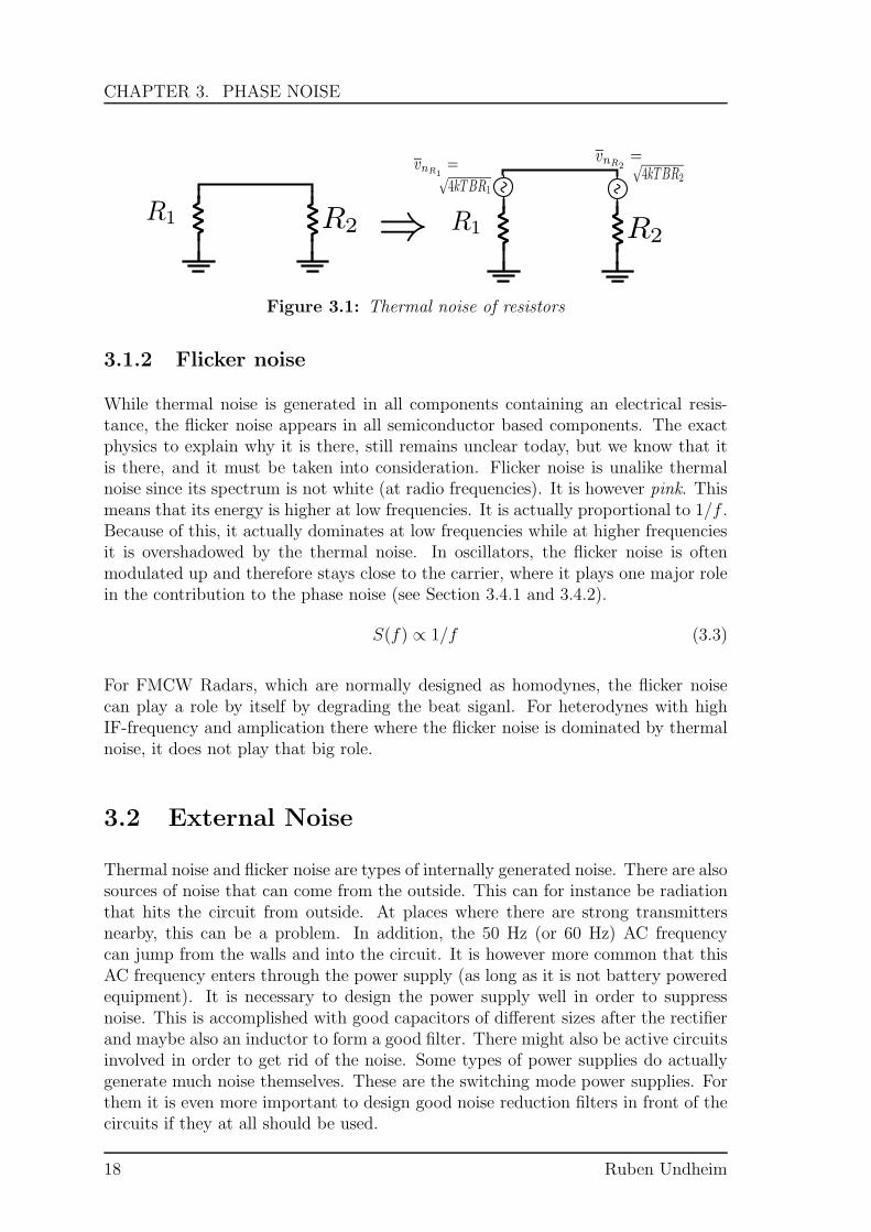
Figure 3.1: Thermal noise of resistors
3.1.2 Flicker noise
While thermal noise is generated in all components containing an electrical resis-tance, the flicker noise appears in all semiconductor based components. The exactphysics to explain why it is there, still remains unclear today, but we know that itis there, and it must be taken into consideration. Flicker noise is unalike thermalnoise since its spectrum is not white (at radio frequencies). It is however pink. Thismeans that its energy is higher at low frequencies. It is actually proportional to 1/f .Because of this, it actually dominates at low frequencies while at higher frequenciesit is overshadowed by the thermal noise. In oscillators, the flicker noise is oftenmodulated up and therefore stays close to the carrier, where it plays one major rolein the contribution to the phase noise (see Section 3.4.1 and 3.4.2).
S(f) ∝ 1/f (3.3)
For FMCW Radars, which are normally designed as homodynes, the flicker noisecan play a role by itself by degrading the beat siganl. For heterodynes with highIF-frequency and amplication there where the flicker noise is dominated by thermalnoise, it does not play that big role.
3.2 External Noise
Thermal noise and flicker noise are types of internally generated noise. There are alsosources of noise that can come from the outside. This can for instance be radiationthat hits the circuit from outside. At places where there are strong transmittersnearby, this can be a problem. In addition, the 50 Hz (or 60 Hz) AC frequencycan jump from the walls and into the circuit. It is however more common that thisAC frequency enters through the power supply (as long as it is not battery poweredequipment). It is necessary to design the power supply well in order to suppressnoise. This is accomplished with good capacitors of different sizes after the rectifierand maybe also an inductor to form a good filter. There might also be active circuitsinvolved in order to get rid of the noise. Some types of power supplies do actuallygenerate much noise themselves. These are the switching mode power supplies. Forthem it is even more important to design good noise reduction filters in front of thecircuits if they at all should be used.
18 Ruben Undheim

3.3. WHAT IS PHASE NOISE?
Besides bypassing capacitors in the power supply, it is important to have bypasscapacitors on the circuit board also preferably very close to the power supply pinsof IC’s when such are used.
3.3 What is Phase Noise?
The output of an ideal oscillator is given by:
s(t) = A0 sin(2πft) (3.4)
In the real world, however, this is an impossible signal. A more correct representationof the output of a real oscillator is given by:
s(t) = A0(1 + ε(t)) sin(2πft+ φ(t)) (3.5)
Frequency (Hz)
Pow
er
Figure 3.2: Simple illustration of phase noise in the frequency plane. The peaksillustrate spurious signals
Here we see two things that were not present in 3.4, ε(t) and φ(t). The first isthe amplitude noise, while the latter is the phase noise. The amplitude noise is thedisturbance of the amplitude of the signal, while phase noise is the disturbance of thephase of the signal. It is also possible to consider the phase noise as frequency noise,since a variation in phase always will be accompagnied by a variation in frequency.1
A typical spectrum of the output of a real oscillator is given in Figure 3.2. On bothsides of the carrier, there is a skirt of noise. In addition to this, there are some peakscaused by spurs. The noise that we see, is actually composed of both the phase noiseand the amplitude noise. In a normal situation with additive noise, the phase noisewill be equal to the amplitude noise in magnitude. This is given by the equiparitiontheorem of thermodynamics [14, p.65]. However, the two categories of noise reactto changes in different ways. An imporant example is in a signal limiter. A perfectlimiter will remove the amplitude noise completely, but not influence the phase noise
1If the phase noise is given by Sφ(f), the frequency noise is given by Sy(f) = f2/f0 ·Sφ(f) [13].
Design of a Linear FMCW Radar Synthesizer 19

CHAPTER 3. PHASE NOISE
at all. In many circuits, there is unvoluntarily a limiting-effect and we are then leftwith the phase noise. For instance a frequency multiplier will amplify phase noise,but keep the amplitude noise unchanged or even remove it. Also, an oscillator itselfwill have a limiting effect and remove the amplitude noise so that the output of anoscillator is dominated by the phase noise. Because of this, we do in most cases onlycare about the phase noise. The amplitude noise is simply already taken care of.The expression for s(t) then looks like:
s(t) = A0 sin(2πft+ φ(t)) (3.6)
Often it is believed that the skirt around the carrier in Figure 3.2 is the phase noiseitself. However, the phase noise is formally defined by IEEE as one half of thespectrum of φ(t) [13].
L(f) = Sφ(f)
2(3.7)
L(f) is often given in dBc/Hz. This spectrum will not be equal to what we see inFigure 3.2, but it is possible to find a relation between the two for frequencies a bitaway from the carrier. In the phase spectrum, the power of the noise will approach∞ as the frequency goes towards 0. In the signal spectrum, on the other hand, thepower will approach the magnitude of the carrier as we approach 0 offset frequency.
It might be confusing to read about phase noise since it can be defined in two ways.The power of the noise in a 1 Hz bandwidth at a certain offset frequency in the signalspectrum divided by the power of the entire signal is one definition. It is measuredin dBc/Hz and here the symbol SRF(∆f) is used for it. The c in dBc means thatit is relative to the carrier. This was actually the former official definition by IEEEfor phase noise before it was changed to the definition above (3.7) in 1997 [13].
SRF(∆f) =power density in one phase noise modulation sideband per Hz
total signal power(3.8)
The power density of φ for a certain frequency offset is measured in rad2/Hz, andnormally referred to 1 rad2/Hz. Its symbol is Sφ(f). It can be shown that for offsetfrequencies not too close to the carrier, the value of Sφ(f) is two times the value ofSRF(∆f). This is the reason for that the definition above (3.7) contains a divisionof 2. When the formal definition was changed they wanted it to remain as similar asbefore. For all cases when we have no amplitude noise and the frequency offset is nottoo small, the value of L(f) might be found just by observing the signal spectrum.L is in the literature usually referred to as the Single Sideband (SSB) phase noise.
To show the relation between the two definitions, we take advantage of Bessel func-tions. Let’s consider φ(t) given as a sine with angular frequency p. This is the same
20 Ruben Undheim

3.3. WHAT IS PHASE NOISE?
Figure 3.3: How the signal spectrum is related to the phase spectrum for the casewith no amplitude noise.a
aThat K is equal to 1 is not ecactly true, but it is what is observed with spectrum analyzers.In theory, it is the entier integrated spectral density that is equal to 1. The exact value of K isonly known for some specific cases like in Equation (3.23)
as saying that the carrier is phase-modulated. The oscillator output of a carrier withthe amplitude equal to 1 can then be written [15, p.10].
s(t) = sin (2πft+ θ sin pt) (3.9)
This may also be written:
s(t) = sin (2πft) cos (θ sin pt) + cos (2πft) sin (θ sin pt) (3.10)
There are two Bessel function properties [16]:
ejx sinφ =∞∑
n=−∞
Jn(x)ejnφ (3.11)
J−n(z) = (−1)nJn(z) (3.12)
Using these, we find two expressions:
cos (x sin φ) = J0(x) + 2[J2(x) cos 2φ+ J4(x) cos 4φ · · · ] (3.13)
sin (x sin φ) = 2[J1(x) sinφ+ J3(x) sin 3φ+ · · · ] (3.14)
With them, we can get a new expression for s(t):
Design of a Linear FMCW Radar Synthesizer 21
CHAPTER 3. PHASE NOISE
s(t) = sin (2πft)[J0(θ) + 2J2(θ) cos(2pt) + 2J4(θ) cos(4pt) + · · · ] (3.15)
+ cos(2πft)[2J1(θ) sin(pt) + 2J3(θ) sin(3pt) + · · · ]
Simplifying this and we get:
s(t) = J0(θ) sin(2πft) + J1(θ) sin((2πf + p)t)− J1(θ) sin((2πf − p)t) (3.16)
+J2(θ) sin((2πf + 2p)t) + J2(θ) sin((2πf − 2p)t) + · · · ]
The Jα(θ)-values are given by:
Jα(θ) =∞∑
m=0
(−1)m
m!Γ(m+ α + 1)
(
1
2θ
)2m+α
(3.17)
When θ is very small which is normally the case for random noise (at least at greateroffsets), this can be simplified to:
J0(θ) ≃ 1
J1(θ) ≃θ
2(3.18)
J2(θ) ≃ J3(θ) ≃ J4(θ) · · · ≃ 0
Now (3.16) can be written
s(t) ≃ J0(θ) sin(2πft) + J1(θ) sin((2πf + p)t)− J1(θ) sin((2πf − p)t) (3.19)
≃ sin(2πft) +θ
2sin((2πf + p)t)− θ
2sin((2πf − p)t) (3.20)
For real noise, we get an infinite number of such sine waves next to each other. Ifthe total phase deviation is small enough, it can be shown based on this that thenoise density has the following relationship:
SRF(∆f) ≈ Sφ(f)
2= L(f) (3.21)
for big enough ∆f .
What we can recognize above is that the phase noise causes sidebands of equalmagnitude at each side of the carrier. Their sign differ however. The spectrum willalways be antisymmetrical around the carrier as long as there is only phase noise.For amplitude noise it can be shown that the spectrum always will be symmetrical
22 Ruben Undheim

3.3. WHAT IS PHASE NOISE?
f_c
f_c+p
f
Figure 3.4: Carrier with added noise in a 1 Hz bandwidth
around the carrier. So in the case when there is noise only at one of the sides, weknow that there must be a combination of phase noise and amplitude noise.
Consider Figure 3.4. There is noise only at one side of the carrier. This implies thatthere is both amplitude noise and phase noise. One can say that the amplitude noisecancels the phase noise at the lower side. Let’s say that we then let the signal gothrough a limiter so that the amplitude noise disappears. What will happen is thatwe suddenly get noise on both sides of the carrier. So by introducing additive noiseat one of the sidebands, we have suddenly created noise on both sides of the carrierby putting it through a limiter [15, p.20-24].
At small frequency offsets, the approximation shown earlier (3.21) does not hold.This is caused by the fact that Sφ(f) gets very big as the offset gets smaller (infact it approaches infinity in a normal oscillator). It has been shown [4] that ifL(f) = h2/f
2, the relation is the following :
L(f) = Sφ(f)
2=
h2
f 2⇒
SRF(f) =h2
(πh2)2 +∆f 2(3.22)
This is the Lorentzian shape - the shape of the squared magnitude of a one-polelowpass filter. It ensures that the carrier does not get infinite power even though thephase noise at 0 frequency offset in the phase spectrum is infinite. It has a value of
SRF (0) =1
h2π2(3.23)
at zero offset. Some other properties of this shape is that the total power of SRF isequal to 1 and that it approaches (3.21) as the frequency offset gets big.
Typical phase noise of an oscillator
An oscillator will typically have a phase noise spectrum that consists of several terms:
L(f) ≈ h4
f 4+
h3
f 3+
h2
f 2+
h1
f+ h0 (3.24)
Design of a Linear FMCW Radar Synthesizer 23

CHAPTER 3. PHASE NOISE
The most important is the h2/f2 term. Nearly all oscillators will have such a slope at
some important offsets, and many approximations of the phase noise are calculatedbased on an ”ideal” oscillator with such a phase noise spectrum. The h4/f
4 term isoften ignored. It appears mainly in the spectra of precision frequency standards atvery low frequencies (below 1 Hz) [17].
When plotting dB-values, the terms in equation 3.24 are correspondingly slopes of-40 dB/decade, -30 dB/decade, -20 dB/decade, -10 dB/decade and constant.
3.4 Why Phase Noise?
Phase noise is the consequence of the contribution from all the different noise com-ponents in the oscillator. The resistors generate thermal noise, the transistors boththermal noise and flicker noise, the power supply provides ripple. These can allcontribute noise which will be transformed into phase noise at the output.
At first we will look into how phase noise appears in a simple LC oscillator. Leesonwas one of the first that tried to make a theory about this in 1966 [2]. His theoryhas been referred to a lot in the literature afterwards. However, as we will see, thetheory has its limitations, and therefore during the last decades there have beenattempts to make even better foundation theories for understanding the phase noisein simple oscillators.
3.4.1 Leeson’s equation
Leesons’s equation is an expression which can be used to estimate the phase noiseof an LC oscillator. [14, p.64-67]
Consider an LC tank in parallel with a resistor and a perfect noiseless energy restor-ing element. The resistor will provide a noise current density of
i2n∆f
= 4kTG =4kT
R(3.25)
If this current is multiplied with the impedance, the voltage is given. The perfectnoiseless energy restoring element will cancel the resistance in the resistor, and hencethe impedance is just the impedance of the LC tank. At a small offset frequency∆ω, from the center frequency, ω0, the impedance may be approximated by
Z(ω0 +∆ω) ≈ jω0L
2∆ωω0
(3.26)
The Q factor is given by
Q =R
ω0L
24 Ruben Undheim
3.4. WHY PHASE NOISE?
and hence the impedance may be written:
|Z(ω0 +∆ω)| ≈ Rω0
2Q|∆ω| (3.27)
The squared mean noise voltage density is therefore given by:
v2n∆f
=i2n∆f
|Z|2 = 4kTR
(
ω0
2Q∆ω
)2
(3.28)
The estimated phase noise in dB is hence given by
L(∆ω) = 10 log
(
v2n2PsigR∆f
)
= 10 log
[
2kT
Psig
(
ω0
2Q∆ω
)2]
(3.29)
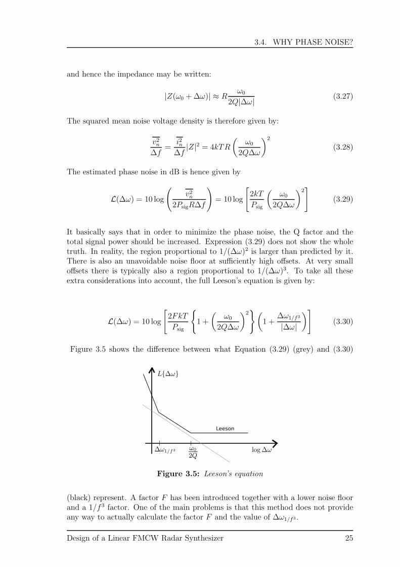
It basically says that in order to minimize the phase noise, the Q factor and thetotal signal power should be increased. Expression (3.29) does not show the wholetruth. In reality, the region proportional to 1/(∆ω)2 is larger than predicted by it.There is also an unavoidable noise floor at sufficiently high offsets. At very smalloffsets there is typically also a region proportional to 1/(∆ω)3. To take all theseextra considerations into account, the full Leeson’s equation is given by:
L(∆ω) = 10 log
[
2FkT
Psig
1 +
(
ω0
2Q∆ω
)2
(
1 +∆ω1/f3
|∆ω|
)
]
(3.30)
Figure 3.5 shows the difference between what Equation (3.29) (grey) and (3.30)
Leeson
Figure 3.5: Leeson’s equation
(black) represent. A factor F has been introduced together with a lower noise floorand a 1/f 3 factor. One of the main problems is that this method does not provideany way to actually calculate the factor F and the value of ∆ω1/f3 .
Design of a Linear FMCW Radar Synthesizer 25

CHAPTER 3. PHASE NOISE
3.4.2 LTV model
Since Leeson’s model contains empirical parameters without showing where theycome from, Lee and Hajmiri developed a new model in 1998 [3]. It considers anoscillator as a time-varying system, and by doing this, much higher insight is achievedinto how the phase noise appears. Earlier texts claimed that to explain differenteffects of the phase noise development in oscillators, it was necessary to considerthe system as nonlinear and they therefore normally skipped any explanation sinceit would become quite complicated. This new model, however, shows that it is notstrictly necessary to consider it as a nonlinear system. The time-variant model,goes far in showing that up-mixing of flicker noise to near-carrier phase noise andthat down-mixing of near-harmonics noise contributes to the 1/f 2 phase noise, isfully possible even when the oscillator is considered a linear system as long as thetime-variation is taken into consideration.
Figure 3.6: Evolution of circuit noise into phase noise (Borrowed from [18, p.331])
Figure 3.6 shows how noise from different frequency bands adds to the phase noise.The flicker-noise (upper Figure to the left) becomes 1/f 3 phase noise in the phasespectrum. The noise near every harmonic of the carrier frequency moves near thecarrier and adds to the 1/f 2 noise. How can it be explained that the noise shiftsfrequency if nonlinearity is not taken into consideration?
The key to understanding this can be found in Figure 3.7. This is the response ofa current impulse in an LC tank that is already oscillating. What can be observedis that the response of the impulse is different depending on where in the cycle itappears. If it appears when the amplitude is maximum (upper), it will not influencethe phase anything. However, when it appears at the same time as the sine is at thezero-crossing (lower), the phase will be shifted. This basically says that the systemis time variant and theories not including time-invariance will fail to explain much
26 Ruben Undheim

3.4. WHY PHASE NOISE?
(like Leeson). It means that in order to minimize the phase noise, it will be good toadd the lost energy (in the oscillator) when the amplitude is at its maximum.
Figure 3.7: Impulse response of LC tank [18, p.329]
The impulse response to the phase of one such pulse can be written:
hφ(t, τ) =Γ(ω0τ)
qmax
u(t− τ) (3.31)
(3.32)
so that the phase response is equal too:
φ(t) =
∫
∞
−∞
hφ(t, τ)i(τ)dτ (3.33)
We see that hφ has two arguments. The τ actually means at what time the pulse isinserted and takes care of the time-invariance. The Γ is a function that will definewhen the impulse makes the biggest influence to the phase. It is called the impulsesensitivity function (ISF). It will be periodic. Since it is periodic it can be expressedas a Fourier series:
Γ(ω0τ) =c02+
∞∑
n=1
cn cos(nω0τ + θn) (3.34)
Setting in for (3.33), we get:
φ(t) =
∫
∞
−∞
hφ(t, τ)i(τ)dτ =1
qmax
∫ t
−∞
Γ(ω0τ)i(τ)dτ
=1
qmax
[
c02
∫ t
−∞
i(τ)dτ +∞∑
n=1
cn
∫ t
−∞
i(τ) cos(nω0τ)dτ
]
(3.35)
If then a sinusoidal current is added which is near an integer multiple m of theoscillation frequency,
i(t) = Im cos[(mω0 +∆ω)t] (3.36)
Design of a Linear FMCW Radar Synthesizer 27

CHAPTER 3. PHASE NOISE
it is found that only the terms where n = m contribute considerably and (3.35) canbe written
φ(t) ≈ Imcm sin(∆ωt)
2qmax∆ω(3.37)
This is interesting because it says that injected noise at frequencies near harmonics ofthe oscillator frequency, ω0, also contribute to the near-carrier phase noise. This wasearlier claimed to be because of nonlinearities, but we see that the time invariancecan cause this behaviour. We see that the influence is scaled by the cm factor. The mis the number of the harmonic, so that if we know all the cm factors for 2 ≤ m < ∞,we will be able to say how much each of the near-harmonics noise bands influence thephase spectrum. Another quite interesting thing is that c0 actually says how muchof the near-0Hz noise that will be upmixed, and this is mainly the flicker noise. Atlast the c1 says how much of the near carrier noise that will be added to the carrierphase noise. Figure 3.6 shows how the noise becomes phase noise. Just one problemremains, how do we find the cm values - or in other words, how do we find the ISF(Γ(ω0τ)). In [3] some methods are explained. It is possible to measure the ISF byinjecting pulses and see the response or one may calculate it. It is referred to [3] fordetails.
3.4.3 Nonlinear models
Even though the LTV method is able to explain how the noise from different fre-quencies adds the phase noise, it is a matter of fact that the oscillator behaviour isnonlinear by nature. So it can be expected that the results obtained will not takeeverything into account and hence not be completely correct. Some approximationsemployed in the LTV method has been shown to be false [19], but still may providegood design intuition. There have been several attempts to analyze the phase noisein a nonlinear system too, and perhaps the most acknowledged of these is presentedby Demir, Mehrotra and Roychowdhury in [4].
The noise is in their work modelled rather differently. If the periodic response of anunperturbed oscillator is given by xs(t), the signal with noise (both amplitude andphase) is described as:
xs(t + α(t)) + y(t) (3.38)
α(t) contains the time shift (phase shift) experienced after time t. It was statedabove that Sφ(f) approaches ∞ as f → 0. That implies that after a certain time,most likely (in practice always) the signal will have a constant phase shift relativeto the beginning. This means that α(t) will in general keep increasing with time.y(t) will on the other hand always remain small because it represents the orbitaldeviation. Nonlinear differential equations are solved and some important resultsare derived. One of them is that the spectrum is Lorentzian near the carrier as
28 Ruben Undheim
3.5. PROPAGATION IN DEVICES
given in (3.22). Another thing is that the oscillator behaviour with noise is shown tobe stationary despite being intuitively hard to understand. It also points out thatwhat is done in the LTV method is in general false.
The article only considers noise appearing from white noise sources, hence only phasenoise with a 1/f 2 characteristic, and it is therefore not straightforward to use theirresult in practical desisgn. It mainly attemps to establish a foundation theory forthe description of phase noise in nonlinear systems, which has been lacking earlier.Based on the huge number of newer articles citing their work, it may be concludedthat they have kind of succeeded with the last thing.
3.5 Propagation in Devices
3.5.1 Mixers
The mixer will preserve the phase noise. It will be added or subtracted dependingon which mixing product that is wanted.
Two perturbed carriers are given by:
s1(t) = sin(2πf1t+ φ1(t))
s2(t) = sin(2πf2t+ φ2(t))
Their product is:
s(t) = s1(t) · s2(t)= sin(2πf1t+ φ1(t)) · sin(2πf2t+ φ2(t))
=1
2cos[2πf1t+ φ1(t)− 2πf2t− φ2(t)]
− 1
2cos[2πf1t+ φ1(t) + 2πf2t+ φ2(t)]
s(t) =1
2cos[2π(f1 − f2)t+ φdifference(t)]
− 1
2cos[2π(f1 + f2)t+ φsum(t)] (3.39)
One of these two terms is then typically selected by a filter since they are at com-pletely different frequencies. For the sum frequency, the phase noise is given by:
φsum(t) = φ1(t) + φ2(t) (3.40)
For the difference frequency:
φdifference(t) = φ1(t)− φ2(t) (3.41)
In FMCW radars, the interest is almost always in the difference frequency, because itis how the beat signal is made. The phase noise will therefore be given by φ1(t)−φ2(t)and as we will see in Chapter 5, this can be made an advantage.
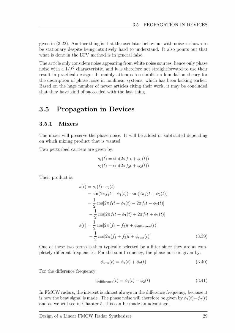
Design of a Linear FMCW Radar Synthesizer 29

CHAPTER 3. PHASE NOISE
3.5.2 Frequency multipliers
The effect of frequency multiplication is also considered [15, p.76]. If a perturbedcarrier is given as:
s1(t) = sin(2πf1t+ θ sin pt) (3.42)
the phase and the instantaneous frequency of the signal is
θsig = 2πf1t+ θ sin pt (3.43)
f1(t) =1
2π
dθsigdt
= f1 +1
2π(pθ cos pt) (3.44)
If the frequency is multiplied by n
f2(t) = nf1(t) = nf1 +1
2π(npθ cos pt) (3.45)
= f2 +1
2π(npθ cos pt)
The phase of this is:
θsig =
∫
2π
(
f2 +npθ
2πcos pt
)
dt
= (2πf2t + nθ sin pt) + C (3.46)
Neglecting the constant C and the new signal is given by:
s2(t) = sin(2πf2t+ nθ sin pt) (3.47)
Hence, the phase noise has been scaled by the frequency multiplication factor n.
φ2 = nφ1 (3.48)
In dB, the relation is
Lout(f) = Lin(f) + 20 logn = Lin(f) + 20 logfoutfin
(3.49)
- an expression which may be very useful.
3.6 Measurement Techniques
The most obvious way to measure phase noise is to use a spectrum analyzer directlyon the signal. The noise observed will have to be scaled according to the bandwidthused when measuring with the formula:
Phase noise in 1 Hz = Noise in RBW− 10 logRBW (3.50)
30 Ruben Undheim

3.6. MEASUREMENT TECHNIQUES
where RBW is the resolution bandwidth used while measuring. In addition, a correc-tion factor which takes into account the implementation of the RBW, the logarithmicdisplay mode and the detector characteristic should be added [20]. Many spectrumanalyzers are capable of doing this scaling automatically. The noise will then begiven in noise power per Hz. By dividing this by the total carrier power, an estimateof L(f) is found. This corresponds to the old definition, SRF, in Equation (3.8)which is measured in dBc/Hz.
However, using a spectrum analyzer directly on the signal has its limitations. Firstof all, as stated above, the skirt around the carrier is composed of both the phasenoise and the amplitude noise. We therefore need to make sure that the amplitudenoise is eliminated. In some cases it can also be assumed that the phase noise andamplitude noise are equally strong and half of the observed power can be attributedto each of them. Another problem is that if the phase noise is low, the spectrumanalyzer needs a very high dynamic range in order to see the phase noise. This iscaused by the fact that the carrier itself is observed at the same time. The carrierfurthermore makes it harder to measure near-carrier phase noise. Because of all this,it is natural that other methods have been developed in order to measure the phasenoise [21].
3.6.1 Down-conversion and filtering of carrier
One possibility is to down-convert the signal to an IF and pass it through a sharpIF filter which removes the carrier while keeping the noise around it. The signalcan then be measured with a spectrum analyzer with the carrier removed and theconstraints on the dynamic range are reduced a lot. Also the noise introduced bythe mixing with the spectrum analyzer’s local oscillator is reduced. The quality ofthe oscillator used for the down-conversion must of course be very good, preferablybetter than the oscillator under test (DUT).
One drawback is that because of the IF filter, it is hard to measure noise closer to thecarrier than 10 kHz. Compared to the previous method it is also slightly harder tocalibrate the measurement. This is because the carrier has been removed. At first,the down-conversion oscillator (LO) must be tuned to a frequency so that the carrierfalls into the passband of the filter and then measure the level of it. Afterwards,the LO must be tuned so that the carrier is removed and then the noise can bemeasured.
3.6.2 Quadrature method
A different method can measure Sφ(f) directly. In order to do this, another stableoscillator with exactly the same frequency is needed. If the two oscillators are mixed,the result after a low-pass filter will be the phase spectrum. It is compulsary thatthe two oscillators are in quadrature - 90 degrees phase shifted to each other. Itmight be quite hard to achieve this, and in cases with a drifting oscillator it ispractically impossible. However, if the two oscillators are very stable and controlled
Design of a Linear FMCW Radar Synthesizer 31

CHAPTER 3. PHASE NOISE
by a synthesizer, it is possible to adjust them exactly to get them in quadrature. Inother cases it is possible to use a Phase-locked loop in order to lock the phase of thesecond oscillator to the first.
This method can measure phase noise really well. It is therefore used to measurehigh performance oscillators, like for instance crystal oscillators. One problem withthis method is that it requires a more complicated calibration than the previousmethods.
3.6.3 Delay line discriminator
A third method measures the frequency noise. It is performed by splitting theoscillator signal in two and then delay one of them 90 and mix them together.After a low-pass filter we have frequency demodulated the signal. It is only possibleto measure noise up to a certain offset frequency, because the discriminator has abandwidth of sinc(πTfm) where the T is the delay of the delay line. This methodworks well for drifting oscillators and it eliminates the amplitude noise just like thequadrature method. However it is not so useful for high-offset noise and for noisevery close to the carrier.
It is also possible to design such an FM detector at an IF frequency. Then thediscriminator can be made better since it is designed for only one frequency. Thesignal must first be mixed down to the IF frequency.
3.7 Jitter
The jitter is the perturbation of the phase seen in time domain. There are severaldefinitions of jitter, but the most common are absolute jitter and period jitter [17].
The absolute jitter is defined as the total time deviation from where a clock transitionwere supposed to be without jitter after time nT0 where T0 is the nominal periodT0 = 1/f0. The standard deviation of the absolute jitter is:
σj abs(T0) ≈1
2πf0
√
∫
∞
0
Sφ(f)df =1
πf0
√
1
2
∫
∞
0
L(f)df (3.51)
The period jitter is the time difference of a single clock period and the ideal clockperiod. It is often more useful than absolute jitter - at least in digital circuits withhigh clock speeds. The period jitter is often also referred to as cycle jitter. Thestandard deviation of the period jitter is:
σj(T0) ≈1
πf0
√
∫
∞
0
2 sin2(πfT0)L(f)df (3.52)
In most cases it does not converge. Then other integration limits can be set, f1 andf2. The lower limit f1 is often given as 10 Hz because everything below 10 Hz is
32 Ruben Undheim

3.7. JITTER
regarded as wandering, and everything above is considered jitter. The upper limitmust be chosen depending on the application and actual phase spectrum. In somecases when f1 is chosen as 10 Hz and f2 kept at ∞, it converges.
A special case is when the phase noise displays a -20 dBc/Hz slope (it is proportionalto 1/f 2). Then the period jitter can be related to the phase noise by:
σj =
√
f 2L(f)f 30
(3.53)
If L(f) = h2/f2, this is the same as:
σj =
√
h2
f 30
(3.54)
The unit of σj is seconds.
In the case with real phase noise which displays a characteristic of -30 dBc/Hz slopeat low offsets, Equation (3.53) is only approximate. It is kind of paradoxal becauseEquation (3.52) in theory diverges when a -30 dBc/Hz slope is present, but stillcrystal oscillators are specified with a small period jitter [17]. This is probablybecause the -30 dBc/Hz slope component causes such a slow variation that it willnot be observed in a short time, and hence the lower integration limit is set to afinite value above 0 in order to find a more practical value of the period jitter.
Design of a Linear FMCW Radar Synthesizer 33

34

Chapter 4
Phase Locked Loops
The Phase Locked Loop is an important part of most of modern day radio equipment.It enables oscillators which are capable of frequency changes (typically VCOs) to bestable and to be easily controlled digitally. The concept consists of using an oscillatorwith a control input which will tune the frequency and a phase detector which willcompare the phase of a reference signal and try to adjust the tunable oscillator sothat its phase is synchronized to the phase of the reference signal. When it is, we saythat the phase is locked to the reference oscillator, thereby the name Phase-LockedLoop.
∼
Ref. Osc.
× ≁≁∼ ∼
VCO
: N
9.2− 9.3GHz
Figure 4.1: Block diagram of PLL
It is also possible to let the VCO be locked to a reference oscillator running atanother frequency if a divider is used before the phase detector. In Figure 4.1, thisis included with the block : N . In addition, a divider can be placed after the referenceoscillator in order to get a fractional relation between the two oscillator frequencies.
When the PLL is in lock, it can be considered a linear control theory system wherethe variable through the loop is phase [17]. In this case, it is possible to use commonlinear control theory techniques in order to analyse the system. The reason for thatwe need to use phase and not amplitude as the variable, is that it is the difference ofthe phases that is compared in the feedback. The phase varies more or less linearlywhile the amplitude follows a sine curve in this part of the loop. Using the amplitudeas the variable would therefore make little sense.
A linearized model of the PLL in lock is presented in Figure 4.2. By looking at this,
35
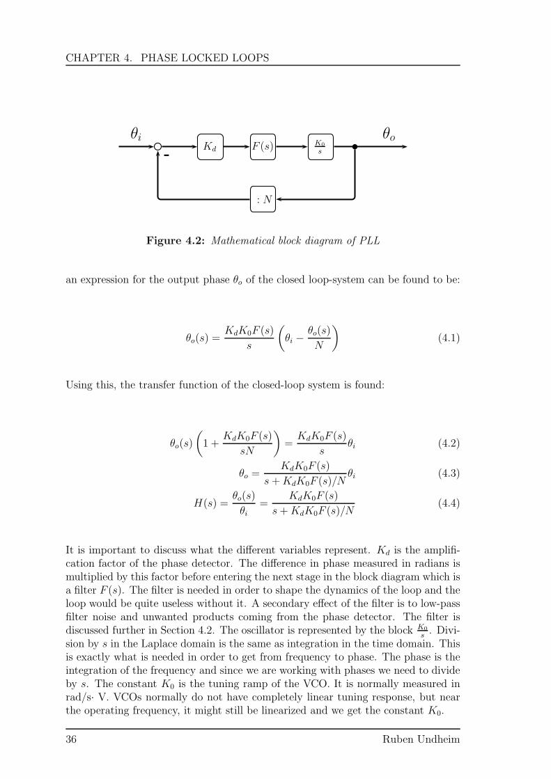
CHAPTER 4. PHASE LOCKED LOOPS
Kd F (s) K0
s
: N
θi θo-
Figure 4.2: Mathematical block diagram of PLL
an expression for the output phase θo of the closed loop-system can be found to be:
θo(s) =KdK0F (s)
s
(
θi −θo(s)
N
)
(4.1)
Using this, the transfer function of the closed-loop system is found:
θo(s)
(
1 +KdK0F (s)
sN
)
=KdK0F (s)
sθi (4.2)
θo =KdK0F (s)
s+KdK0F (s)/Nθi (4.3)
H(s) =θo(s)
θi=
KdK0F (s)
s+KdK0F (s)/N(4.4)
It is important to discuss what the different variables represent. Kd is the amplifi-cation factor of the phase detector. The difference in phase measured in radians ismultiplied by this factor before entering the next stage in the block diagram which isa filter F (s). The filter is needed in order to shape the dynamics of the loop and theloop would be quite useless without it. A secondary effect of the filter is to low-passfilter noise and unwanted products coming from the phase detector. The filter isdiscussed further in Section 4.2. The oscillator is represented by the block K0
s. Divi-
sion by s in the Laplace domain is the same as integration in the time domain. Thisis exactly what is needed in order to get from frequency to phase. The phase is theintegration of the frequency and since we are working with phases we need to divideby s. The constant K0 is the tuning ramp of the VCO. It is normally measured inrad/s· V. VCOs normally do not have completely linear tuning response, but nearthe operating frequency, it might still be linearized and we get the constant K0.
36 Ruben Undheim

4.1. PHASE DETECTORS
4.1 Phase Detectors
There are different types of phase detectors (PD). The most basic is the mixer. Itperforms a multiplication of the two inputs, and one of the products (after low-passfiltering) is the sine of the phase difference. We therefore have a sinusoidal responseof the phase difference, but as long as the difference is small, the sine is a goodapproximation of a linear function.
If the reference oscillator signal vr(t) and the oscillator signal vo(t) are given by,
vr(t) = A1 sin(ωt+ θr) (4.5)
vo(t) = A2 cos(ωt+ θo) (4.6)
the output of the mixer with gain Km is given by
vd(t) = Kmvi(t)vo(t)
=1
2KmA1A2 sin(θr − θo) +
1
2KmA1A2 sin(2ωt+ θr + θo) (4.7)
It can be observed that after lowpass-filtering, the output is the sine of the phasedifference scaled with
Kd =KmA1A2
2(4.8)
For small phase errors, the sine will be very much like a linear function. Note thatfor this phase detector, the PLL locks when the inputs are near 90 phase shiftedto each other. In many cases it is desired to have the phase shift equal to 0. Thiscan be accomplished by adding a delay even though it will not be perfect for allfrequencies.
This mixer phase detector only detects phase difference. If the two oscillators operateat two different frequencies, it will not necessarily be able to lock them to each other.As long as the frequency difference is not too big, it will handle it because of pull-ineffects, but the speed that the pull-in effect works at does not get higher when thefrequency difference is higher. It will therefore not be good when a big tuning rangeis wanted. It may need some time to get in lock if it actually gets in lock at all.What is necessary, is some way to also measure the frequency difference and use thisin order to lock the oscillators quickly to each other. The most popular method fordoing this is with a Phase-Frequency Detector (PFD).
4.1.1 PFD
The Phase-Frequency Detector was most likely first presented in 1971 by BrownJ.I [22], and since then it has become very popular and it is used in most frequencysynthesizers nowadays. The PFD is a sequential detector. That implies that it is de-pendent on zero-transitions of the signal in order to track the phase (and frequency)difference. Because of this, it is not good when there is very much noise involved.
Design of a Linear FMCW Radar Synthesizer 37

CHAPTER 4. PHASE LOCKED LOOPS
R
L
UP
DOWN
"1"
"1"
Delay
D Q
CLR
D Q
CLR
Figure 4.3: A basic PFD
However, it works very well when the signals are clean. Figure 4.3 explains how itcan be made.
The output of the PFD are an UP-signal and a DOWN-signal. They indicate thedirection of the frequency change that is needed. Every time they both are active atthe same time, they will both after a very short delay turn off again. When they areoff, the state that the PD is in is called a zero-state and it means that no changes ofthe tuning voltage are needed. It is this third state which enables it to also indicatethe direction and magnitude of a frequency difference.
The two digital outputs, UP and DOWN, must be transformed into a voltage sincethe VCO is controlled by a voltage. This can be accomplished in several ways. Onemethod is to use a charge pump [23]. It is a circuit that lets each of the two outputscontrol each their current sources. If UP is active, current is sinked to the output,if DOWN is active, current is drawn from the output. If then there is a capacitorattached to the output, there will be a varying voltage over it. Instead of usinga charge pump it is possible to let the two outputs be attached to a differentialintegrator implemented with an op-amp.
4.2 Filter
For all the different implementations of a phase detector above it is absolutely nec-essary to have a filter after them in order to control the dynamics of the loop. Thisfilter is referred to as the loop filter. It will also low-pass filter the tuning signal inorder to remove noise, but that is just a secondary effect which we will not be soconcerned about. PLLs are classified depending on how many integrators they havein the loop. There is always one integrator in the VCO because it changes a phasedifference into a frequency. Therefore all PLLs are at least of Type 1. Possibly otherintegrators must be built into the filter. It can be shown that in order to have nostatic phase difference between the two oscillators, the PLL must at least be of type2.
The filter may be either passive or active. What is best to use depends on the PD
38 Ruben Undheim

4.2. FILTER
(a) An active filter
R1
C1
C2
(b) A filter for a charge pumpPFD
(c) An active differential filter
Figure 4.4: Showing 3 common types of loop filters
type, the VCO tuning voltage range, and the need for extra integrators in the filter.For example will the charge pump based PD not need an active filter in order to getan extra integrator (see Figure 4.4(b)), while other PD types always will need anactive filter in that case. Furthermore, if the tuning voltage of the VCO exceeds themaximum output of the phase detector voltage, there will be a need for an activefilter.
Transfer function of an active integrator filter
Consider Figure 4.4(a). The transfer function of this filter is given by:
F (s) =R2 +
1sC1
R1
=sR2C1 + 1
sR1C1
(4.9)
Transfer function of a charge pump filter
For the case with a charge pump, the circumstances are a bit different. Since thecharge pump provides a constant current, Ip, over a certain time equal to the phaseshift in each cycle, it is necessary to consider the case when the oscillator frequencyis much higher than the loop bandwidth. Then the average current supplied to theloop filter is given by [17]:
Design of a Linear FMCW Radar Synthesizer 39
CHAPTER 4. PHASE LOCKED LOOPS
id =Ipθe2π
(4.10)
The PD gain is hence Kd = Ip/2π. The transfer function of the entire PLL is givenby
H(s) =K0IpZF (s)/2π
s+K0IpZF (s)/2π(4.11)
where ZF (s) is the impedance of the loop filter. By looking at Figure 4.4(b), theimpedance can be found to be:
ZF (s) =sC2
+ 1C1C2R1
s2 + sC1R1
+ sC2R1
(4.12)
In fact, the capacitor C2 is not strictly needed in order to have the desired integratoreffect of the loop filter, but it is good to have since it prevents big spikes reachingthe loop filter.
4.3 Full Transfer Function
If the filter with an active integrator is used, the transfer function of the filter isgiven as:
F (s) =sR2C + 1
sR1C(4.13)
By putting this into the expression for H(s), we get:
H(s) =KdK0
(
sR2C+1sR1C
)
s + KdK0
N
(
sR2C+1SR1C
)
=KdK0
R2
R1
s+ KdK0
R1C
s2 + s(
KdK0R2
NR1
)
+ KdK0
NR1C
(4.14)
This is an expression for the closed-loop response of a Type-2 second-order PLL. Bynoting that a general expression for a second order transfer function can be givenas:
Hgeneral(s) =N (2ζωns+ ω2
n)
s2 + 2ζωns+ ω2n
(4.15)
Expressions for the natural frequency, ωn, and the damping factor, ζ , are found tobe:
40 Ruben Undheim
4.4. TRACKING
ωn =
√
KdK0
NR1Cζ =
R2
2
√
CKdK0
NR1
(4.16)
The natural frequency in Hz, fn, later also referred to as the loop bandwidth is givenby:
fn =ωn
2π=
1
2π
√
KdK0
NR1C(4.17)
These can be used to predict the behaviour of the PLL.
4.4 Tracking
When the PLL is in lock, changes of the reference oscillation frequency will betracked by the VCO. As long as the changes are not too abrupt, the PLL will stayin lock and track the changes smoothly.
For a type 2 PLL, the phase error after a frequency step is given by [17]
θe(t) =∆ω
ωn
(
1√
1− ζ2sin√
1− ζ2ωnt
)
e−ζωnt (4.18)
for ζ < 1 and
θe(t) =∆ω
ωn
(
1√
ζ2 − 1sinh
√
ζ2 − 1ωnt
)
e−ζωnt (4.19)
for ζ > 1.
What needs to be ensured in order to keep the PLL locked, is that the phase errorgiven by the expression above always stays much smaller than 2π. Exactly how muchsmaller, depends on what kind of phase detector that is used. By differentation of(4.18) and (4.19), we get the frequency error.
ωe(t) = ∆ω cos(√
1− ζ2ωnt)e−ζωnt −∆ω
(
1√
1− ζ2sin√
1− ζ2ωnt
)
ζe−ζωnt
(4.20)
for ζ < 1. And for ζ > 1:
ωe(t) = ∆ω cosh(√
ζ2 − 1ωnt)e−ζωnt −∆ω
(
1√
ζ2 − 1sinh
√
ζ2 − 1ωnt
)
ζe−ζωnt
(4.21)
Figure 4.5 and 4.6 are plots of (∆ω − ωe(t))/2π for different values of ωn. It showshow the VCO will track a frequency step in the reference. The higher the value ofωn, the faster the VCO will settle at the desired frequency.
Design of a Linear FMCW Radar Synthesizer 41
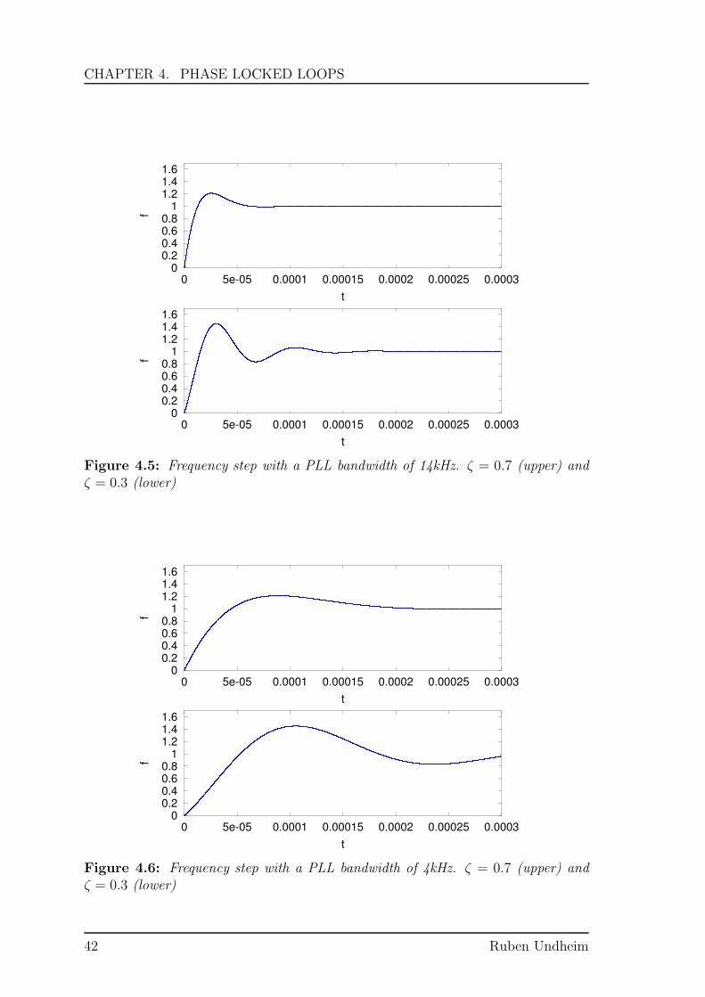
CHAPTER 4. PHASE LOCKED LOOPS
00.20.40.60.8
11.21.41.6
0 5e-05 0.0001 0.00015 0.0002 0.00025 0.0003
f
t
00.20.40.60.8
11.21.41.6
0 5e-05 0.0001 0.00015 0.0002 0.00025 0.0003
f
t
Figure 4.5: Frequency step with a PLL bandwidth of 14kHz. ζ = 0.7 (upper) andζ = 0.3 (lower)
00.20.40.60.8
11.21.41.6
0 5e-05 0.0001 0.00015 0.0002 0.00025 0.0003
f
t
00.20.40.60.8
11.21.41.6
0 5e-05 0.0001 0.00015 0.0002 0.00025 0.0003
f
t
Figure 4.6: Frequency step with a PLL bandwidth of 4kHz. ζ = 0.7 (upper) andζ = 0.3 (lower)
42 Ruben Undheim
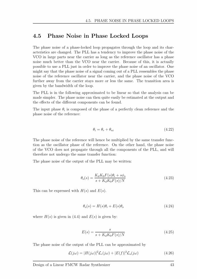
4.5. PHASE NOISE IN PHASE LOCKED LOOPS
4.5 Phase Noise in Phase Locked Loops
The phase noise of a phase-locked loop propagates through the loop and its char-acteristics are changed. The PLL has a tendency to improve the phase noise of theVCO in large parts near the carrier as long as the reference oscillator has a phasenoise much better than the VCO near the carrier. Because of this, it is actuallypossible to use a PLL just in order to improve the phase noise of an oscillator. Onemight say that the phase noise of a signal coming out of a PLL ressembles the phasenoise of the reference oscillator near the carrier, and the phase noise of the VCOfurther away from the carrier stays more or less the same. The transition area isgiven by the bandwidth of the loop.
The PLL is in the following approximated to be linear so that the analysis can bemade simpler. The phase noise can then quite easily be estimated at the output andthe effects of the different components can be found.
The input phase θi is composed of the phase of a perfectly clean reference and thephase noise of the reference:
θi = θr + θni (4.22)
The phase noise of the reference will hence be multiplied by the same transfer func-tion as the oscillator phase of the reference. On the other hand, the phase noiseof the VCO does not propagate through all the components of the PLL, and willtherefore not undergo the same transfer function:
The phase noise of the output of the PLL may be written:
θo(s) =KdK0F (s)θi + sφo
s+KdK0F (s)/N(4.23)
This can be expressed with H(s) and E(s).
θo(s) = H(s)θi + E(s)θo (4.24)
where H(s) is given in (4.4) and E(s) is given by:
E(s) =s
s +KdK0F (s)/N(4.25)
The phase noise of the output of the PLL can be approximated by
L(jω) = |H(jω)|2Lc(jω) + |E(f)|2Lo(jω) (4.26)
Design of a Linear FMCW Radar Synthesizer 43
CHAPTER 4. PHASE LOCKED LOOPS
where Lc(jω) is the phase noise of the reference and Lo(jω) is the phase noise ofthe open-loop VCO. The noise that appear in the divider and the phase detectorwill add to the phase noise of the reference signal and hence also be multiplied by|H(jω)|. When working with dB, these expressions can be used:
Ldue-to-reference(f) = Lref(f) + 20 log |H(f)| (4.27)
Ldue-to-open-loop-vco(f) = Lvco(f) + 20 log |E(f)| (4.28)
The loop filter noise will add to the phase noise like this [17]:
Ldue to loop filter =|E(f)|2K2
0Sn filter
(2πf)2(4.29)
where Sn filter is the one-sided spectrum of the loop filter noise1.
-140
-120
-100
-80
-60
-40
-20
0
101
102
103
104
105
106
Phase n
ois
e d
Bc/H
z
Offset frequency Hz
PLL Bandwidth 30kHz, PD Freq 121MHz
Free running VCOPhase-locked VCO
Figure 4.7: How the PLL will modify the phase noise of a VCO
Figure 4.7 presents how the phase noise of the output of a PLL typically will changewhen the reference oscillator is very much cleaner than the VCO near the carrier.The open-loop VCO is in blue, and the closed-loop VCO in green.
1This is noise and not phase noise
44 Ruben Undheim

Chapter 5
Degradation Effects in FMCWRadars
5.1 Phase Noise
The phase noise is the most important degradation effect for FMCW Radars andit plays a much bigger role than for pulse radars. It influences the performance inseveral ways. The main issue is that the radar transmits and receives simultaneously.The signal will therefore leak from the transmitter directly to the receiver. This willhappen through space, and perhaps even more severely if the transmitter and thereceiver share the same circuit board, through the substrate. The leakage signal1
may be so strong that it may saturate either the low-noise amplifier or the mixer.However, a more common problem is that the phase noise that also leaks will havea tendency to mask out targets since the targets are detected at frequency offsets ofthe carrier. The same is the case for strong nearby clutter.
Frequency
Targets
Convers
ion p
roduct
Figure 5.1: How targets can be masked by the phase noise
In the mixer of the receiver, the transmit signal is injected so that it can be mixedwith the received signal. It can be seen that the phase noise of the transmitted signaland the received signal are to some degree correlated, and that this effect can beexploited in order to improve the performance. This is especially true for the direct
1The leakage signal is sometimes called spillover.
45
CHAPTER 5. DEGRADATION EFFECTS IN FMCW RADARS
leakage at the radar site. In fact, most radars based on FMCW principles would notbe very sensitive if this correlation were not exploited.
The correlation can be found by setting up an expression for the phase noise differ-ence ∆φ(t) [24]. td is the time back and forth to the target:
∆φ(t) = φ(t− td)− φ(t) (5.1)
The autocorrelation is then:
R∆φ(τ) = E[φ(t+ τ − td)− φ(t+ τ)][φ(t− td)− φ(t)]= E[φ(t+ τ − td)φ(t− td)]−E[φ(t + τ)φ(t− td)]
−E[φ(t+ τ − td)φ(t)] + E[φ(t+ τ)φ(t)]
= Rφ(τ)− Rφ(td + τ)− Rφ(τ − td) +Rφ(τ)
= 2Rφ(τ)−Rφ(td + τ)− Rφ(τ − td) (5.2)
By taking the fourier transform of the autocorrelation, the spectrum density is found.
S∆φ(f) = FR∆φ(f) = 2Sφ(f)− Sφ(f)e−j2πftd − Sφ(f)e
j2πftd (5.3)
= 2Sφ(f)(1− cos(2πftd))
= 2Sφ(f)(1− cos(2πlf/c))
S∆φ(f) = 4Sφ(f)sin2(πlf/c) (5.4)
As can be seen, the spectrum density of the phase noise difference is given as4 sin2(πlf/c) times the spectrum density of the phase noise of the transmitted signal.The factor l is the path length between the two signals. It is only the phase noisedifference that plays a role because the receiver mixes the transmitted signal withthe received signal, and if the phase noise difference between the two signals is zero,the beat signal will contain no phase noise. If for example the path length l is zero,the phase noise will cancel completely. This can be exploited by making the delayof the transmitter leakage exactly as long as the delay from the transmitter to themixer. It should also be noted that the effect is greater at low frequency offsets, f .From Equation (5.4) a cancellation factor, C, can be defined as is done in [1].
C = 4 sin2(πlf/c) (5.5)
Note that this cancellation will only affect the phase noise - not the amplitudenoise. In addition, even if there were complete cancellation (C = 0), there wouldbe nonlinear elements that transform amplitude noise into phase noise [1] and hencethe phase noise will not be completely eliminated. It should also be noted that thefactor is periodical along the frequency offset axis. At some offsets it will reduce thephase noise, while at others it will make it higher because of the 4.
If there are targets with strong reflection, the phase noise that is also reflected willhave a tendency to mask out weaker targets. This could also cause problems. Itis therefore very important to make the phase noise of the transmitter as low aspossible.
46 Ruben Undheim

5.1. PHASE NOISE
-200
-180
-160
-140
-120
-100
-80
-60
-40
-20
102
103
104
105
106
107
108
dB
c/H
z
Offset frequency Hz
Original VCO phase noisePath difference 0.1 m
0.5 m20 m
200 m1000 m
Figure 5.2: Cancellation effect of phase noise because of correlation. The oscillatoris the open-loop VCO used in the design (Table 6.2 page 61).
Figure 5.2 presents the cancellation effect for different path length differences. Itcan be seen that the periodicity of the cancellation factor is first really having aneffect for targets far away. If the path length error in the transmitter is 10 cm, thephase noise is very much cancelled as indicated by the green line and it may even beso good that the noise spectrum will be dominated by thermal noise (not indicatedin the figure).
5.1.1 Contribution to the unaccuracy of the distance esti-mation
In addition to having a tendency to mask out the signal, the phase noise will alsocontribute to the unaccuracy of the signals that are detected. This will lead toa uncertainty in the range and bearing measurements that can be expressed as avariance. The frequency estimation error of an FFT when there is a systematicphase error has been shown to be [25]:
δω ∼=
N−1∑
n=0
δϕ[n] · (∆t · n− t0)w(δt · n− t0)∆t
∞∫
−∞
t2w(t)dt
(5.6)
This is based on a deterministic phase error, and must hence be adapted to thestochastic case with noise variance. The FFT window function is represented by the
Design of a Linear FMCW Radar Synthesizer 47

CHAPTER 5. DEGRADATION EFFECTS IN FMCW RADARS
w(t). It is expected that the same cancellation effect, C, will play a role also for theaccuracy. That means, that at closer ranges, the phase error will not be that big asexpected from the phase noise spectrum.Clearly, there are many factors influencingthe measurement accuracy and not just phase noise. The receiver noise performanceis also among them.
When the target is not moving, the distance error due to phase error can be foundfrom (5.6) and (2.8) to be:
δr ∼=cN−1∑
n=0
δϕ[n] · (∆t · n− t0)w(δt · n− t0)∆t
2α∞∫
−∞
t2w(t)dt
(5.7)
where α is the sweep rate and c the speed of light.
5.2 Linearity and Quantization of Sweep
The sweep that is generated should be very linear and clean. If it does not followa linear curve, the range resolution will be reduced as pointed out in [26]. When aDDS is employed to generate the sweep, the main issue is however not nonlinearity,but quantization. The sweep consists of many small steps. These will in somecases influence the capability of the radar, but as we will see, if everything is donecorrectly, they will play no big role. [11, p. 42-45]
05000
10000150002000025000300003500040000
-60000 -40000 -20000 0 20000 40000 60000
am
plit
ude
frequency offset (Hz)
0
200000
400000
600000
800000
1e+06
1.2e+06
1.4e+06
0 0.0001 0.0002 0.0003 0.0004 0.0005 0.0006
tranm
it fre
quency (
Hz)
time (s)
Figure 5.3: Beat signal when using unquantized sweep
48 Ruben Undheim
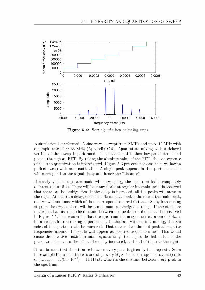
5.2. LINEARITY AND QUANTIZATION OF SWEEP
0
5000
10000
15000
20000
25000
-60000 -40000 -20000 0 20000 40000 60000
am
plit
ude
frequency offset (Hz)
0
200000
400000
600000
800000
1e+06
1.2e+06
1.4e+06
0 0.0001 0.0002 0.0003 0.0004 0.0005 0.0006
tranm
it fre
quency (
Hz)
time (s)
Figure 5.4: Beat signal when using big steps
A simulation is performed. A sine wave is swept from 2 MHz and up to 12 MHz witha sample rate of 33.33 MHz (Appendix C.4). Quadrature mixing with a delayedversion of the sweep is performed. The beat signal is then low-pass filtered andpassed through an FFT. By taking the absolute value of the FFT, the consequenceof the step quantization is investigated. Figure 5.3 presents the case then we have aperfect sweep with no quantization. A single peak appears in the spectrum and itwill correspond to the signal delay and hence the ”distance”.
If clearly visible steps are made while sweeping, the spectrum looks completelydifferent (figure 5.4). There will be many peaks at regular intervals and it is observedthat there can be ambiguities. If the delay is increased, all the peaks will move tothe right. At a certain delay, one of the ”false”peaks takes the role of the main peak,and we will not know which of them correspond to a real distance. So by introducingsteps in the sweep, there will be a maximum unambiguous range. If the steps aremade just half as long, the distance between the peaks doubles as can be observedin Figure 5.5. The reason for that the spectrum is non-symmetrical around 0 Hz, isbecause quadrature mixing is performed. In the case with normal mixing, the twosides of the spectrum will be mirrored. That means that the first peak at negativefrequencies around -16000 Hz will appear at positive frequencies too. This wouldcause the effective maximum unambiguous range to be just the half. Half of thepeaks would move to the left as the delay increased, and half of them to the right.
It can be seen that the distance between every peak is given by the step rate. So infor example Figure 5.4 there is one step every 90µs. This corresponds to a step rateof fstep rate = 1/(90 · 10−6) = 11.11kHz which is the distance between every peak inthe spectrum.
Design of a Linear FMCW Radar Synthesizer 49
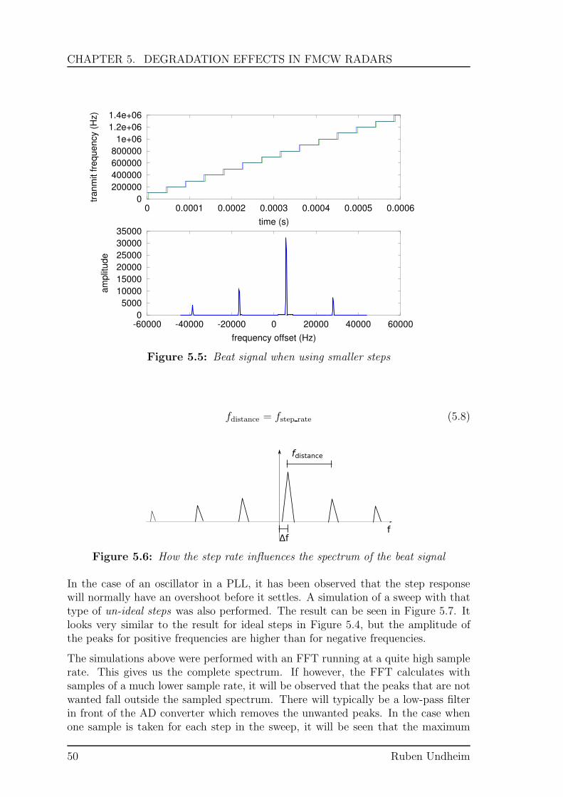
CHAPTER 5. DEGRADATION EFFECTS IN FMCW RADARS
0
5000
10000
15000
20000
25000
30000
35000
-60000 -40000 -20000 0 20000 40000 60000
am
plit
ude
frequency offset (Hz)
0
200000
400000
600000
800000
1e+06
1.2e+06
1.4e+06
0 0.0001 0.0002 0.0003 0.0004 0.0005 0.0006
tranm
it fre
quency (
Hz)
time (s)
Figure 5.5: Beat signal when using smaller steps
fdistance = fstep rate (5.8)
fdistance
Δff
Figure 5.6: How the step rate influences the spectrum of the beat signal
In the case of an oscillator in a PLL, it has been observed that the step responsewill normally have an overshoot before it settles. A simulation of a sweep with thattype of un-ideal steps was also performed. The result can be seen in Figure 5.7. Itlooks very similar to the result for ideal steps in Figure 5.4, but the amplitude ofthe peaks for positive frequencies are higher than for negative frequencies.
The simulations above were performed with an FFT running at a quite high samplerate. This gives us the complete spectrum. If however, the FFT calculates withsamples of a much lower sample rate, it will be observed that the peaks that are notwanted fall outside the sampled spectrum. There will typically be a low-pass filterin front of the AD converter which removes the unwanted peaks. In the case whenone sample is taken for each step in the sweep, it will be seen that the maximum
50 Ruben Undheim

5.2. LINEARITY AND QUANTIZATION OF SWEEP
0
5000
10000
15000
20000
-60000 -40000 -20000 0 20000 40000 60000
am
plit
ude
frequency offset (Hz)
0
200000
400000
600000
800000
1e+06
1.2e+06
1.4e+06
0 0.0001 0.0002 0.0003 0.0004 0.0005 0.0006
tranm
it fre
quency (
Hz)
time (s)
Figure 5.7: Beat signal when using practical steps
unambiguous range as a consequence of the low-pass filter before the sampling is thesame as the maximum unambiguous range because of the stepping. So the conclusionwill be that the steps play no big role as long as not more samples are taken thanthe number of steps.
However, there is one thing that should be noticed. The not-wanted peaks stealsome of the energy from the ideal peak. In Figure 5.3, the amplitude is about 35000,while it is just 23000 in Figure 5.4. It basically says that the radar sensitivity canbe a bit reduced if this is not taken into consideration.
Design of a Linear FMCW Radar Synthesizer 51

52
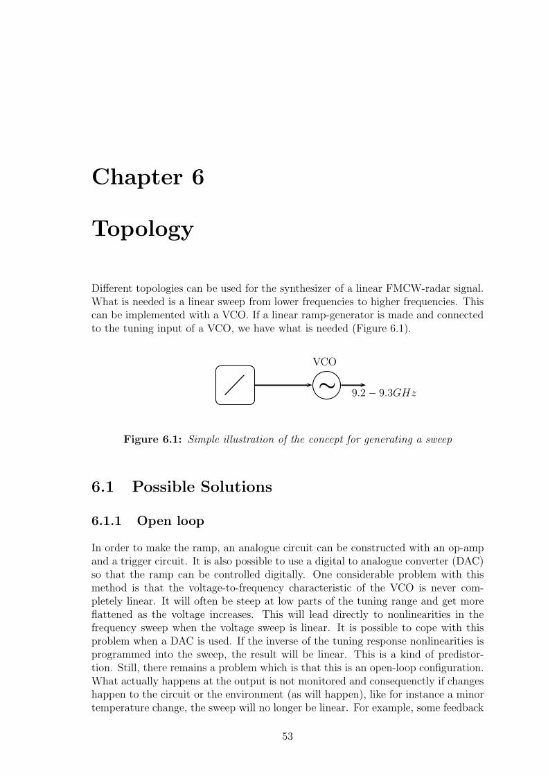
Chapter 6
Topology
Different topologies can be used for the synthesizer of a linear FMCW-radar signal.What is needed is a linear sweep from lower frequencies to higher frequencies. Thiscan be implemented with a VCO. If a linear ramp-generator is made and connectedto the tuning input of a VCO, we have what is needed (Figure 6.1).
∼
VCO
9.2− 9.3GHz
Figure 6.1: Simple illustration of the concept for generating a sweep
6.1 Possible Solutions
6.1.1 Open loop
In order to make the ramp, an analogue circuit can be constructed with an op-ampand a trigger circuit. It is also possible to use a digital to analogue converter (DAC)so that the ramp can be controlled digitally. One considerable problem with thismethod is that the voltage-to-frequency characteristic of the VCO is never com-pletely linear. It will often be steep at low parts of the tuning range and get moreflattened as the voltage increases. This will lead directly to nonlinearities in thefrequency sweep when the voltage sweep is linear. It is possible to cope with thisproblem when a DAC is used. If the inverse of the tuning response nonlinearities isprogrammed into the sweep, the result will be linear. This is a kind of predistor-tion. Still, there remains a problem which is that this is an open-loop configuration.What actually happens at the output is not monitored and consequenctly if changeshappen to the circuit or the environment (as will happen), like for instance a minortemperature change, the sweep will no longer be linear. For example, some feedback
53
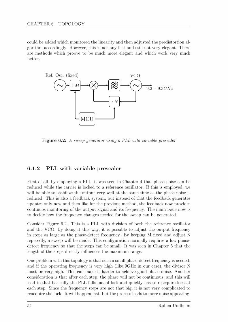
CHAPTER 6. TOPOLOGY
could be added which monitored the linearity and then adjusted the predistortion al-gorithm accordingly. However, this is not any fast and still not very elegant. Thereare methods which proove to be much more elegant and which work very muchbetter.
∼
Ref. Osc. (fixed)
: M × ≁≁∼ ∼
VCO
: N
9.2− 9.3GHz
MCU
Figure 6.2: A sweep generator using a PLL with variable prescaler
6.1.2 PLL with variable prescaler
First of all, by employing a PLL, it was seen in Chapter 4 that phase noise can bereduced while the carrier is locked to a reference oscillator. If this is employed, wewill be able to stabilize the output very well at the same time as the phase noise isreduced. This is also a feedback system, but instead of that the feedback generatesupdates only now and then like for the previous method, the feedback now providescontinuos monitoring of the output signal and its frequency. The main issue now isto decide how the frequency changes needed for the sweep can be generated.
Consider Figure 6.2. This is a PLL with division of both the reference oscillatorand the VCO. By doing it this way, it is possible to adjust the output frequencyin steps as large as the phase-detect frequency. By keeping M fixed and adjust Nrepetedly, a sweep will be made. This configuration normally requires a low phase-detect frequency so that the steps can be small. It was seen in Chapter 5 that thelength of the steps directly influences the maximum range.
One problem with this topology is that such a small phase-detect frequency is needed,and if the operating frequency is very high (like 9GHz in our case), the divisor Nmust be very high. This can make it harder to achieve good phase noise. Anotherconsideration is that after each step, the phase will not be continuous, and this willlead to that basically the PLL falls out of lock and quickly has to reacquire lock ateach step. Since the frequency steps are not that big, it is not very complicated toreacquire the lock. It will happen fast, but the process leads to more noise appearing.
54 Ruben Undheim

6.1. POSSIBLE SOLUTIONS
∼
TCXO 1GHz
DDS × ≁≁∼ ∼
VCO
: N
9.2− 9.3GHz
MCU
≁≁∼
Figure 6.3: Using a DDS as the reference to the PLL. The frequency of the VCOoutput is divided while the DDS output is only filtered.
6.1.3 DDS as the reference oscillator for the PLL
Figure 6.3 shows another very interesting configuration. Here a DDS (Direct DigitalSynthesis, see Appendix D) circuit is employed. The need for a very linear sweepis very often nowadays accomodated with the use of a DDS. It lets us output allthe frequencies we want up to a frequency of about 40% of the frequency of itsreference oscillator, and it can be controlled directly digitally. An MCU will set theconfiguration parameters of the DDS, and the output signal will then be used as thereference of the PLL. This provides a number of advantages. DDS circuits normallyhave continuous phase which implies that the frequency steps can be accepted bythe PLL without loosing lock. The step response will be more or less exactly ascalculated with the Equations in Section 4.4. Furthermore, it is possible to makethe DDS produce very small steps and adjust them precisely.
The output frequency will be given by N times the DDS generated frequency. Thesize of the steps at the output of the DDS will correspondingly be scaled by N. Stillthe steps at the VCO can be made remarkably small as the DDS steps may be setas small as a fraction of a Hz!
The transfer function of the PLL in this configuration is the same as in Chapter 4because only the VCO frequency is followed by a divider.
H(s) =θo(s)
θi=
KdK0F (s)
s+KdK0F (s)/N(6.1)
As we saw in that same chapter, the phase noise near the carrier will mainly begiven by the frequency of the reference oscillator scaled by N , and that the phasenoise further away will be given by the VCO itself. The near-carrier phase noise willtherefore normally be made better than when the VCO runs freely. The focus onchoosing a VCO with low near-carrier phase noise, is therefore not that important,but the phase noise further away from the carrier must be good (the two normallyfollow each other though). At the same time, the output of the DDS must be
Design of a Linear FMCW Radar Synthesizer 55

CHAPTER 6. TOPOLOGY
provided with very low near-carrier phase noise. This is often the main issue. Thenoise will be scaled by N which makes it even harder. All in all, this configurationis a very much employed one.
∼
TCXO 1GHz
DDS × ≁≁∼ ∼
VCO(4.60− 4.65GHz)
: N
9.2− 9.3GHzMCU
≁≁∼
x2
Figure 6.4: Equal to the previous one just with a frequency doubler at the output.
With frequency doubler
Figure 6.4 shows another topology that can be used. It is different because it uses anadditional frequency doubler after the VCO. The topology is not very much different.Some VCOs are even implemented with a frequency doubler internally. It must beused if the operating frequency is so high that good oscillators cannot be found.When a frequency doubler is used afterwards, it must be ensured that the doublerdoes not add much more noise. The phase noise will, as we have seen earlier, bescaled by the factor N for frequency multiplication, and since here N is 2, the phasenoise will be scaled by 2, or 20 log 2 dB.
∼
TCXO 1GHz
DDS × ≁≁∼ ∼
VCO
×∼ Osc. 9GHz
9.2− 9.3GHz
MCU
≁≁∼
≁≁∼200− 300MHz
Figure 6.5: PLL having frequency conversion in the loop.
56 Ruben Undheim

6.1. POSSIBLE SOLUTIONS
PLL with frequency conversion within the loop
Let us have a look at some other topologies too. Figure 6.5 is a variation of theformer topology in that it uses down-conversion in the loop [15]. Yet another fixedfrequency oscillator is needed for this. The result of frequency-conversion is differentfrom the prescaler. The phase noise will not be scaled down, but it will be addedjust as if nothing happened to it.
-140
-130
-120
-110
-100
-90
-80
-70
101
102
103
104
105
106
Phase n
ois
e d
Bc/H
z
Offset frequency Hz
PLL Bandwidth 30kHz, PD Freq 121MHz
No frequency conversionfLO = 2 GHz
4 GHz6 GHz9 GHz
Figure 6.6: Predicted phase noise for the topology with frequency conversion in theloop and an ideal oscillator
A Laplace expression can be made for this case to see how it differs. To make thecase more general, a prescaling factor, N , is included between the mixer and thephase detector.
θo(s) =KdK0F (s)
s
(
θi −θo(s) + θLO
N
)
(6.2)
θo(s)
(
1 +KdK0F (s)
sN
)
=KdK0F (s)
sθi −
KdK0F (s)
sNθLO (6.3)
θo =KdK0F (s)
s+KdK0F (s)/N(θi −
θLON
) (6.4)
The transfer function for the two different sources of noise will be given by
H(s) =θo(s)
θi=
KdK0F (s)
s+KdK0F (s)/N(6.5)
HLO(s) =θo(s)
θLO=
KdK0F (s)/N
s+KdK0F (s)/N(6.6)
Design of a Linear FMCW Radar Synthesizer 57

CHAPTER 6. TOPOLOGY
-140
-130
-120
-110
-100
-90
-80
-70
101
102
103
104
105
106
Phase n
ois
e d
Bc/H
z
Offset frequency Hz
PLL Bandwidth 30kHz, PD Freq 121MHz
No frequency conversionfLO = 2 GHz
4 GHz6 GHz9 GHz
Figure 6.7: Predicted phase noise for the topology with frequency conversion in theloop with an oscillator with equal phase noise performance as the TCXO
-140
-120
-100
-80
-60
-40
101
102
103
104
105
106
Phase n
ois
e d
Bc/H
z
Offset frequency Hz
PLL Bandwidth 30kHz, PD Freq 121MHz
No frequency conversionfLO = 2 GHz
4 GHz6 GHz9 GHz
Figure 6.8: Predicted phase noise for the topology with frequency conversion in theloop with an oscillator 20 dB worse than the TCXO
58 Ruben Undheim

6.1. POSSIBLE SOLUTIONS
This means that the the noise from the second oscillator will add directly to theoutput. It will not be scaled by the N factor as the reference signal will. On theother hand, since the N factor will be much lower than for the previous topology,the noise from the reference will no longer be scaled as much up. This will be anadvantage. It has to be weighed against the contribution of the noise from thesecond oscillator. All in all, this topology can be very good. The main disadvantageis probably that another high quality oscillator is needed along with a good mixerand a low-pass filter. This makes it quite a bit more expensive. Furthermore, theDDS must be swept over a larger bandwidth since its steps are not scaled by a bigN, and consequently it might be harder to eliminate spurs from it.
Figure 6.6 presents a comparison between the topology with frequency conversionin the loop and without (for code see Appendix C.1). Equation (6.5) and (6.6) areused in the calculation. In this case, the local oscillator has been considered ideal,thus not contributing any noise. It can be seen that the total phase noise of the PLLdecreases as the frequency conversion frequency gets higher. It is observed that thereis definitely something to be gained by using frequency conversion. If the oscillator isno longer considered ideal, as in figure 6.7 , the phase noise reduction becomes muchlower. In this case, a local oscillator with the same phase noise performance as theTCXO (which is very good) scaled by fLO/fTCXO (see Section 3.5) has been used. Inthe case when the local oscillator, or the combination of the local oscillator and themixer, have 20 dB more phase noise than the TCXO for all offset frequencies, thephase noise of the output becomes much worse when frequency conversion is added(Figure 6.8).
All in all it may be concluded that the gain achieved with frequency conversiondepends heavily on the performance of the oscaillator, and it must be judged if it isworth the cost.
∼
TCXO 1GHz
DDS ≁≁∼
MCU
×∼
Osc. 9GHz
∼≁≁9.2− 9.3GHz
Figure 6.9: Direct mixing of the DDS signal with a fixed frequency oscillator.
Design of a Linear FMCW Radar Synthesizer 59

CHAPTER 6. TOPOLOGY
6.1.4 DDS output mixed directly with fixed oscillator
The topology seen in Figure 6.9 is different from the previous because it does notnecessarily use a PLL. The output of the DDS is mixed directly with the outputof a fixed frequency oscillator. In this case, the phase noise of the output will begiven as the sum of the phase noise of the two oscillators. Since they both can bemade very good, the total phase noise can be made very good. A very importantconsideration for this topology is that the bandpass filter following the mixer mustbe made very good. If it is not, the image frequency will also propagate through.That is, if a 9 GHz fixed oscillator is used and the DDS outputs at 200MHz, therewill be an output at both 8.8 GHz and 9.2 GHz. The filter must have a very highattenuation at 8.8 GHz if the desired output is at 9.2 GHz. The mixer must also bemade good so that it does not add much phase noise.
Another thing to mention with this topology is that the sweep from the DDS mustbe made much wider. It will not be scaled anything as in the previous configurations.To get a sweep from 9.2 to 9.3 GHz, the DDS must sweep from 200 MHz to 300MHz. For the topology in Figure 6.3 using a division factor of for instance 100, thesweep would be only from 92 MHz to 93 MHz.
To get a very good phase noise performance of the last configuration, the fixedfrequency oscillator should be phase locked to an external reference. A TCXO hasa very good near-carrier phase noise, but it is often worse than a VCO at offsetsfurther away from the carrier. By locking the VCO to an external TCXO, we willget the best from the two devices as we have seen in the previous chapter. It canfor example be locked to the same TCXO as is used as the reference of the DDS inorder to save money. This implies that the VCO should run at an integer-multiplyfrequency of the DDS reference.
6.2 Chosen Topology
It was decided to implement the topology with a DDS as a reference and withoutfrequency conversion (Figure 6.3). This was done because it has many good prop-erties and still the design is pretty straight forward. No expensive filters or mixersare needed. The phase noise performance is quite good, but it will depend on thefrequency conversion frequency that is used.
The VCO must by itself provide low phase noise. This is especially true for offsetsfar away from the carrier since there the noise will not be attenuated by the PLL. Itis also important that the VCO has the desired tuning range, and that the tuningrange is not too large for the application. If it is, the noise coming in through thetuning input will play a bigger role. The VCO should also have a reasonable strongoutput so that not too much amplification is needed afterwards which will furtherdegrade the phase noise. Table 6.1 presents different VCOs capable of outputting9.2 GHz directly. Their performance were compared, and the oscillator HMC510from Hittite Microwave Technologies was chosen. Its phase noise performance ispresented in Table 6.2.
60 Ruben Undheim

6.2. CHOSEN TOPOLOGY
Company Name Freq V Vtune dBm 10kHz 100kHzHittite HMC734LP5 8600-10200 5.0 1-13 18 -70 -100Hittite HMC510LP5 8450-9550 5.0 0-15 13 -92 -116Hittite HMC511LP5 9050-10150 5.0 2-13 13 -88 -115Hittite HMC587LC4B 5000-10000 5.0 0-18 5 -65 -95RFMD RFVC1834 9000-10200 5.0 2-12 8 -90RFMD RFVC1833 8300-9700 5.0 2-12 8 -90RFMD RFVC1800 8000-12000 5.0 0-13 4 -66RFMD RFVC1801 5000-10000 5.0 0-18 4 -72RFMD RFVC1800C 8000-12000 5.5 0-13 4 -66Synergy DXO900965-5 9000-9650 5.0 0-12 -3 -80 -100
Table 6.1: Comparison of different VCOs capable of 9.2-9.3 GHz
Frequency offset dBc/Hz100Hz -221kHz -5510kHz -92100kHz -1151MHz -135
Table 6.2: SSB Phase noise of the HMC510 from Hittite Microwaves [27]
Frequency offset dBc/Hz100Hz -921kHz -12110kHz -141100kHz -1471MHz -150
Table 6.3: SSB Phase noise of the VFTX210 from Valpey Fisher [28]
Frequency offset dBc/Hz1kHz -14710kHz -150100kHz -152
Table 6.4: SSB Phase noise of the AD9858 DDS at fout = 103 MHz [29]
Design of a Linear FMCW Radar Synthesizer 61
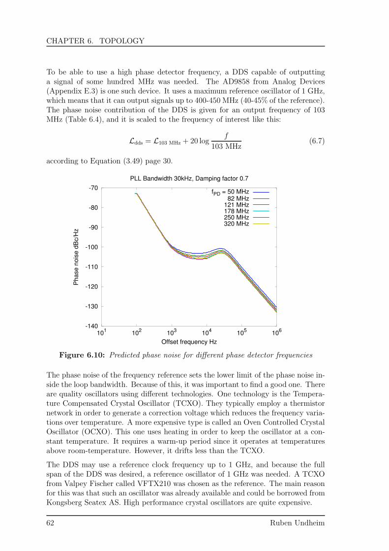
CHAPTER 6. TOPOLOGY
To be able to use a high phase detector frequency, a DDS capable of outputtinga signal of some hundred MHz was needed. The AD9858 from Analog Devices(Appendix E.3) is one such device. It uses a maximum reference oscillator of 1 GHz,which means that it can output signals up to 400-450 MHz (40-45% of the reference).The phase noise contribution of the DDS is given for an output frequency of 103MHz (Table 6.4), and it is scaled to the frequency of interest like this:
Ldds = L103 MHz + 20 logf
103 MHz(6.7)
according to Equation (3.49) page 30.
-140
-130
-120
-110
-100
-90
-80
-70
101
102
103
104
105
106
Phase n
ois
e d
Bc/H
z
Offset frequency Hz
PLL Bandwidth 30kHz, Damping factor 0.7
fPD = 50 MHz82 MHz
121 MHz178 MHz250 MHz320 MHz
Figure 6.10: Predicted phase noise for different phase detector frequencies
The phase noise of the frequency reference sets the lower limit of the phase noise in-side the loop bandwidth. Because of this, it was important to find a good one. Thereare quality oscillators using different technologies. One technology is the Tempera-ture Compensated Crystal Oscillator (TCXO). They typically employ a thermistornetwork in order to generate a correction voltage which reduces the frequency varia-tions over temperature. A more expensive type is called an Oven Controlled CrystalOscillator (OCXO). This one uses heating in order to keep the oscillator at a con-stant temperature. It requires a warm-up period since it operates at temperaturesabove room-temperature. However, it drifts less than the TCXO.
The DDS may use a reference clock frequency up to 1 GHz, and because the fullspan of the DDS was desired, a reference oscillator of 1 GHz was needed. A TCXOfrom Valpey Fischer called VFTX210 was chosen as the reference. The main reasonfor this was that such an oscillator was already available and could be borrowed fromKongsberg Seatex AS. High performance crystal oscillators are quite expensive.
62 Ruben Undheim

6.2. CHOSEN TOPOLOGY
-140
-120
-100
-80
-60
-40
-20
0
101
102
103
104
105
106
Phase n
ois
e d
Bc/H
z
Offset frequency Hz
PLL Damping factor constant 0.7, PD Freq 121MHz
fn = 0 kHz5 kHz
15 kHz30 kHz50 kHz80 kHz
100 kHz
Figure 6.11: Predicted phase noise for different loop bandwidths
6.2.1 Phase noise predictions
Using the equations in Section 4.5 and the data for the phase noise of the differentcomponents, the phase noise was plotted for different situations. All the plots includephase noise effects from the VCO, the TCXO, the DDS, the phase detector, and theloop filter.
First figure 6.10 presents different phase detector frequencies. It is observed that thetotal phase noise is reduced as the frequency gets higher, or N lower. There is a greatimprovement from 50 MHz to 100 MHz, so lower frequencies should not be used.It was decided to use a divisor of 76, giving an output of 121.053 MHz to 122.368MHz. The images and harmonic spurs of the DDS for these output frequencies aregiven in Table 6.5.
Number MHz1 877.6 - 878.92 755.3 - 757.93 632.9 - 636.84 510.5 - 515.85 388.2 - 394.76 265.8 - 273.77 143.4 - 152.68 21.0 - 31.6
Table 6.5: Main image frequencies and harmonic spurs of the DDS with an outputat 121 MHz. (see Appendix D)
Design of a Linear FMCW Radar Synthesizer 63

CHAPTER 6. TOPOLOGY
-140
-130
-120
-110
-100
-90
-80
-70
101
102
103
104
105
106
Phase n
ois
e d
Bc/H
z
Offset frequency Hz
PLL Bandwidth 30kHz, PD Freq 121MHz
ζ = 0.70.10.41.02.05.0
10.0
Figure 6.12: Predicted phase noise for different damping factors
Figure 6.11 present the effect of changing the loop bandwidth. It is observed thatit influences the phase noise spectrum quite much. The damping constant is keptconstant, while the loop bandwidth is changed from 0 to 100 kHz. When it is 0, thephase noise spectrum is only affected by the VCO, and hence the spectrum is thesame as for the VCO in an open-loop condition (Table 6.2). It is observed that forvery high loop bandwidths, the phase noise inside the loop bandwidth is lower, butit decreases more slowly at higher offsets. The point where the phase noise of thereference scaled by N is equal to the phase noise of the VCO, all the curves almostpass through. By choosing the loop bandwidth as a frequency near this point, boththe phase noise inside the loop bandwidth and outside the bandwidth can be madelow. A loop bandwidth of about 20 - 30 kHz seems to be a good choice for a totallow phase noise.
For the case when the bandwidth is kept constant and the damping factor is adjusted,the phase noise influence can be seen in Figure 6.12. The lower the damping factor,the higher peak there will be near the loop bandwidth frequency. This is not desired,so the damping factor must be chosen high enough. When the damping is veryhigh, the phase noise outside the loop bandwidth decreases much more slowly. It isconcluded that there is a lot to be gained from the inside bandwidth phase noise bygoing from ζ = 0.1 to ζ = 1.0, but at increasing values of ζ , there is not much of adecrease. The ideal choice seems to be between 0.7 and 1.5.
64 Ruben Undheim
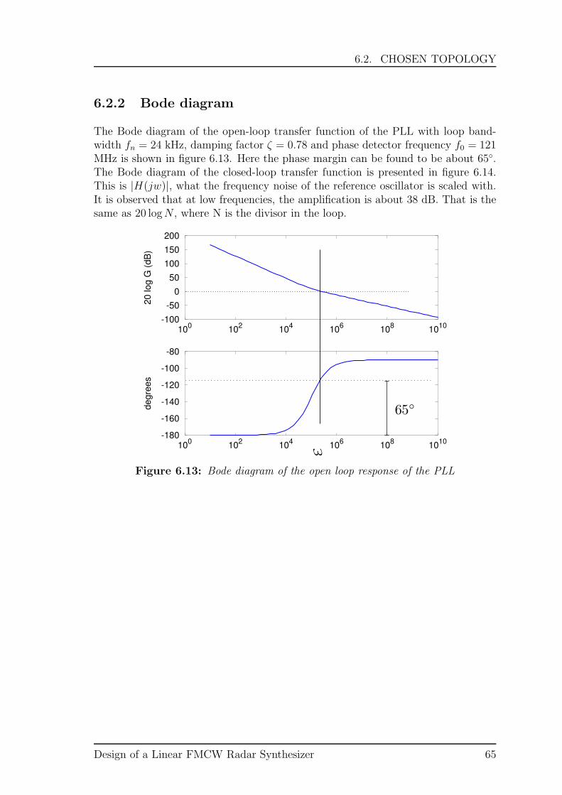
6.2. CHOSEN TOPOLOGY
6.2.2 Bode diagram
The Bode diagram of the open-loop transfer function of the PLL with loop band-width fn = 24 kHz, damping factor ζ = 0.78 and phase detector frequency f0 = 121MHz is shown in figure 6.13. Here the phase margin can be found to be about 65.The Bode diagram of the closed-loop transfer function is presented in figure 6.14.This is |H(jw)|, what the frequency noise of the reference oscillator is scaled with.It is observed that at low frequencies, the amplification is about 38 dB. That is thesame as 20 logN , where N is the divisor in the loop.
-180
-160
-140
-120
-100
-80
100
102
104
106
108
1010
degre
es
-100
-50
0
50
100
150
200
100
102
104
106
108
1010
20 log G
(dB
)
Figure 6.13: Bode diagram of the open loop response of the PLL
Design of a Linear FMCW Radar Synthesizer 65

CHAPTER 6. TOPOLOGY
-80
-60
-40
-20
0
20
40
100
102
104
106
108
1010
20 log H
(dB
)
f
Figure 6.14: Bode diagram of the closed loop response of the PLL
66 Ruben Undheim

Chapter 7
Circuit Design
A synthesizer for a linear FMCW radar in the 9.2-9.3 GHz band was to be designedand built. The requirements were mainly low phase noise and the capability of alinear sweep. Figure 7.1 presents the chosen topology - now with component namesincluded. The choice of the VCO, the DDS and the VCO was presented in theprevious chapter. This chapter presents the other components and how the wholecircuit was designed.
∼
VFTX210
AD9858 ×HMC698
≁≁∼ ∼
HMC510
: N
9.2− 9.3GHz
ATtiny2313
≁≁∼
Figure 7.1: Block diagram of the design
7.1 Components
7.1.1 VCO
The VCO (HMC510) comes in a 32 lead 5x5 mm SMT package [27]. It is poweredwith 5 V and draws nominally 315 mA. The power output is claimed to be between+10 and +15 dBm at the operating frequency 8.45 - 9.55 GHz. There are alsoa divide-by-2 and divide-by-4 output. Only the divide-by-4 was used to provide
67
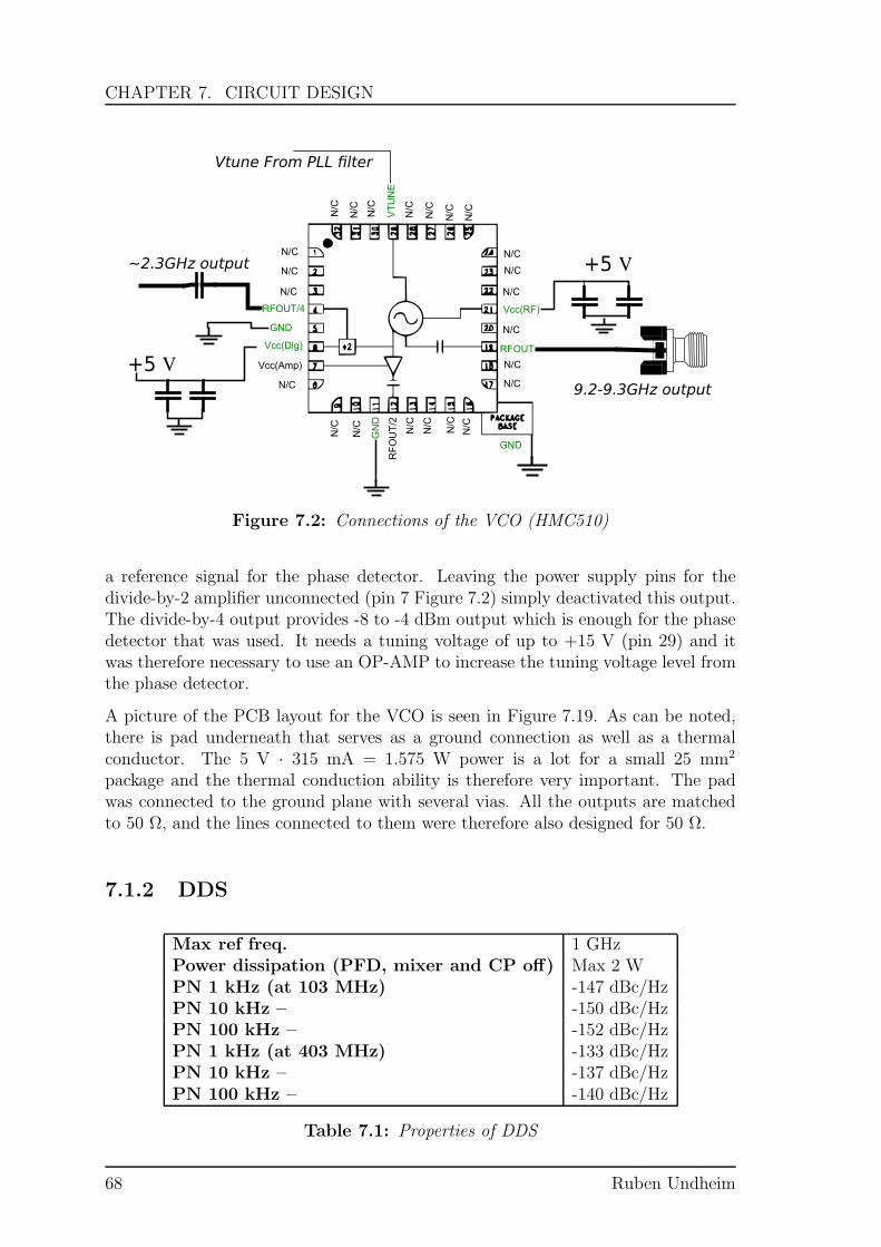
CHAPTER 7. CIRCUIT DESIGN
N/C
RFOUT/4
GND
Vcc(Dlg)
Vcc(Amp)
Vcc(RF)
RFOUT
RFOUT/2
N/C
N/C
N/C
N/C
N/C
N/C
GND
N/C
N/C
N/C
N/C
N/C
N/C
N/C
N/C
N/CVTUNE
N/C
N/C
N/C
N/C
N/C
N/C
N/C
GND
+5 V
+5 V
9.2-9.3GHz output
~2.3GHz output
Vtune From PLL filter
Figure 7.2: Connections of the VCO (HMC510)
a reference signal for the phase detector. Leaving the power supply pins for thedivide-by-2 amplifier unconnected (pin 7 Figure 7.2) simply deactivated this output.The divide-by-4 output provides -8 to -4 dBm output which is enough for the phasedetector that was used. It needs a tuning voltage of up to +15 V (pin 29) and itwas therefore necessary to use an OP-AMP to increase the tuning voltage level fromthe phase detector.
A picture of the PCB layout for the VCO is seen in Figure 7.19. As can be noted,there is pad underneath that serves as a ground connection as well as a thermalconductor. The 5 V · 315 mA = 1.575 W power is a lot for a small 25 mm2
package and the thermal conduction ability is therefore very important. The padwas connected to the ground plane with several vias. All the outputs are matchedto 50 Ω, and the lines connected to them were therefore also designed for 50 Ω.
7.1.2 DDS
Max ref freq. 1 GHzPower dissipation (PFD, mixer and CP off) Max 2 WPN 1 kHz (at 103 MHz) -147 dBc/HzPN 10 kHz – -150 dBc/HzPN 100 kHz – -152 dBc/HzPN 1 kHz (at 403 MHz) -133 dBc/HzPN 10 kHz – -137 dBc/HzPN 100 kHz – -140 dBc/Hz
Table 7.1: Properties of DDS
68 Ruben Undheim

7.1. COMPONENTS
The DDS comes in a 100 pin TQFP EP package (See Figure 7.3). This is one ofthe reasons for that a proper PCB was needed. Most of the pins are actually powersupply and grounding. The digital and analogue parts of the chip are separated sodifferent grounds and supplies can be connected. In this design, a common groundwas used, but the power supplies were separated so that bypassing could be donefor each of them separately.
Figure 7.3: Picture of the DDS
The steering can be performed either with a parallel interface or a serial interface.This is selected by setting the pin SPSELECT either high or low. The parallelinterface uses 8 data pins and 5 address pins together with some handshaking pins.This requires a big microcontroller or an FPGA. However, the serial interface canbe used with only 3 wires (Chip select included). It permits using a much smallermicrocontroller. The maximum speed that can be used to control is given by SYN-CLK which is the reference oscillator divided by 8. It is obvious that the parallelinterface allows higher speed controlling than the serial interface since whole bytescan be clocked at the rate of the SYNCLK instead of just single bits. When theserial interface is used, the register address must be sent separately before the datainstead of parallely with its own pins. A last complication is that the serial interfaceonly allows changing whole 32-bit words at a time, while the parallel interface canchange the value of 8-bit parts of these words at a time. However, since the parallelinterface needs so many more control wires, it was decided to use the serial interfaceto accommodate the use of a small MCU.
There is also an internal phase detector and mixer in the AD9858. However, eventhough a phase detector was needed in the design, this one was not used since itsspecification was not good enough. This caused even more pins of the DDS to remainunconnected.
Design of a Linear FMCW Radar Synthesizer 69
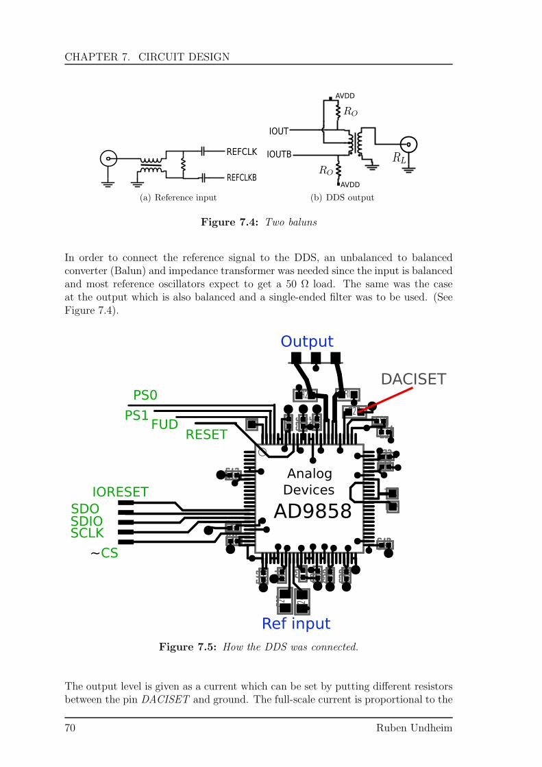
CHAPTER 7. CIRCUIT DESIGN
REFCLK
REFCLKB
(a) Reference input
IOUT
IOUTB
AVDD
AVDD
(b) DDS output
Figure 7.4: Two baluns
In order to connect the reference signal to the DDS, an unbalanced to balancedconverter (Balun) and impedance transformer was needed since the input is balancedand most reference oscillators expect to get a 50 Ω load. The same was the caseat the output which is also balanced and a single-ended filter was to be used. (SeeFigure 7.4).
Ref input
Output
DACISETPS0
PS1FUD
RESET
IORESET
SDOSDIOSCLK
~CS
Analog
Devices
AD9858
Figure 7.5: How the DDS was connected.
The output level is given as a current which can be set by putting different resistorsbetween the pin DACISET and ground. The full-scale current is proportional to the
70 Ruben Undheim
7.1. COMPONENTS
resistor value as [29]:
RSET = 39.19/IMAX (7.1)
A resistor of 1.96 kΩ was used. 1.96 kΩ yields IMAX = 20 mA as the maximumcurrent. The DDS is capable of 40 mA output at maximum, but because of reducednoise and spuriosity at lower currents, 20 mA was chosen. [29] states that the bestspurious-free dynamic range (SFDR) is given at this value.
In order to match to 50 Ω, the resistors RO and the winding ratio N of the trans-former at the output had to be scaled accordingly. N defines the output power likethis [30]:
PL =RL
2
(
IMAX
4N
)2
(7.2)
where RL is the desired output impedance, in this case 50 Ω. For N = 1/2, this is:
PL =50
2
(
20 mA
4 · 1/2
)2
= 2.5 mW ≈ +4 dBm (7.3)
It seems like the output power from the DDS can be made infinitely high by choosingN very small, but in addition to having a maximal current output, it also has amaximum peak voltage of 0.5 V. The reference input of the phase detector acceptsinputs of -5 to +5 dBm, so more output power than +4 dBm is not needed. Tomatch, the resistors RO were given values according to [30]:
RO =RL
2N2=
50
2 · (1/2)2 = 100 Ω (7.4)
They were connected from IOUT and IOUTB to AVDD as indicated in the datasheet[29].
To avoid mistakes and to get inspiration, the official evaluation board [31] was studiedintensively. Among other things, the same input and output transformers were used.The layout of the power plane (Figure 7.16(c)) was also heavily inspired by thedesign.
The registers in the DDS had to be set to the desired values (see Appendix E.3).First of all, the 2 GHz divider had to be disabled by setting bit 6 in the controlregister 0x00. For fixed frequency output the frequency is set with the register FTWand given by:
fOUT =(FTW × SY SCLK)
232(7.5)
where SYSCLK in our case is 1 GHz. The value of FTW can thus be calculatedlike this:
FTW =fOUT × 232
SY SCLK(7.6)
Design of a Linear FMCW Radar Synthesizer 71

CHAPTER 7. CIRCUIT DESIGN
t
f
Figure 7.6: How the registers in the DDS controls the automatic sweep
When using the automatic sweep function, the frequency steps are set by
∆f =DFTW × SY SCLK
232(7.7)
and the time between every step by
∆t =8×DFRRW
SY SCLK(7.8)
Consider also figure 7.6 for the registers used when sweeping. In order to start thesweep, bit 15 of the control register is set. See Appendix A for details on how theAD9858 was controlled.
Many power supply pins are present on the AD9858. All of them were individuallybypassed with capacitors directly to the ground plane. Figure 7.5 shows them to-gether with all the output and inputs used. The digital connections are green whilethe RF connections are blue.
7.1.3 Low-pass filter
The phase detector frequency was 121 MHz, and because of the Nyquist imagesgenerated (Appendix D), a low-pass filter was needed at the DDS output. Thecutoff frequency was set to about 200 MHz. This would then also allow the testingof other phase detector frequencies up to about 200 MHz. A 5-pole Chebyshev0.1 dB ripple filter referred to 50 Ω was constructed as figure Figure 7.7 presents.This was found using an Internet low-pass filter calculator [32]. It would also bepossible to use prototype tables with standard values and adapt to the correct cutofffrequency and circuit impedance.
The frequency response of the filter is plotted in figure 7.8. To make the filter, chipinductors and capacitors were used.
7.1.4 Microcontroller
The microcontroller AVR ATtiny2313 from Atmel was chosen because of its smallsize and easy programming. It was programmed using an Atmel AVR ISP mkII
72 Ruben Undheim
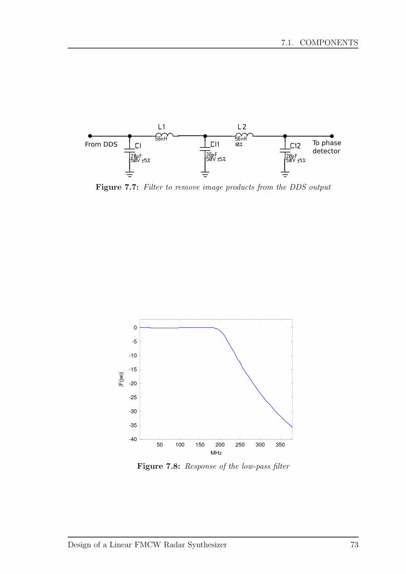
7.1. COMPONENTS
From DDS To phase
detector
Figure 7.7: Filter to remove image products from the DDS output
-40
-35
-30
-25
-20
-15
-10
-5
0
50 100 150 200 250 300 350
|F(jw
)|
MHz
Figure 7.8: Response of the low-pass filter
Design of a Linear FMCW Radar Synthesizer 73

CHAPTER 7. CIRCUIT DESIGN
Programmer connected to the computer with USB. The controller code was writtenin C and compiled using gcc-avr and avr-libc (Refer to Appendix A for the sourcecode). It was transferred to the circuit using avrdude. All of the three are availableas open source software in the Ubuntu package repository. The connections thatwere needed to program the MCU are presented in Appendix B.
The MCU has a built-in clock oscillator at 8 MHz which is divided by 8 inside thechip by default so that the effective clock rate is 1 MHz. It was decided to use serialprogramming of the DDS and hence not so many pins of the MCU were used.
A file ad9858control.c was developed (see Appendix A.1) with many functions forthe serial communication It was desired to let the synthesizer be controlled with a
Figure 7.9: Pinout of AVR ATtiny2313 [33]
computer. Since the computer can cause much noise to be transferred to the board, itwas decided to use an optocoupler for the communication. By using an optocoupler,galvanic isolation can be achieved and the noise from a connected computer can beeliminated to some degree.
+3.3VTo RS232 Board
TXD
GND
RXDPin 2 - PD0\RXD
Pin 3 - PD1\TXD
To ATtiny2313
Figure 7.10: How the galvanic isolation was achieved with an optocoupler
7.1.5 Phase detector
Max ref freq. 1.3 GHzPN 10 kHz square wave clock 100MHz -153 dBc/HzPN 10 kHz sine wave clock 100MHz -148 dBc/HzTotal current 310 mA
Table 7.2: Properties of phase detector [34]
74 Ruben Undheim

7.1. COMPONENTS
The phase detector from Hittite, HMC698, was chosen because of its high perfor-mance. It is a PFD without a charge pump. The output is however a differentialvoltage. There is a divider inside and the division factor can be set with externaljumpers from 12 to 159.
The phase noise floor of the phase detector is given both for sinusoidal reference inputand square wave reference input. The square wave is definitely better. However,in our case, the input will be sinusoidal, and hence the phase noise floor is at -148dBc/Hz at most offset frequencies. This can be converted to the frequency of interest[35] by using the formula:
Lfrom PLL = LPLL at 100MHz + 10 log
(
f
100 MHz
)
(7.9)
To choose the divisor, there are 8 pins that must be set either high or low. In orderto allow experimentation, a place was made for jumpers on the board. In addition,a LED was connected to the lock-detect output of the phase detector to indicatewhen the PLL is in lock. This can be very useful.
7.1.6 Loop filter
NU
ND
+15V
Figure 7.11: Schematic of the loop-filter
The filter used was a differential integrator. To the left in Figure 7.11 are capacitorsfor jump suppression (C4 and C5) [23]. To the right is a filter with a pole far outsidethe bandwidth of the loop. If these are ignored for now, the output voltage of theop-amp is given by.
Vout = Av(V+ − V −) (7.10)
where V + is:
V + = VND
(
R4 +1
sC2
R4 +1
sC2+ R3
)
(7.11)
Design of a Linear FMCW Radar Synthesizer 75
CHAPTER 7. CIRCUIT DESIGN
and:
V − = VNU
(
R2 +1
sC1
R2 +1
sC1+R1
)
+ Vout
(
R1
R2 +1
sC1+R1
)
(7.12)
If Av ≫ 1, the output of the op-amp can be found to be:
Vout = VND
(
R4 +1
sC2
R1
)(
R1 +R2 +1
sC1
R3 +R4 +1
sC2
)
− VNU
(
R2 +1
sC1
R1
)
(7.13)
In the case when R1 = R3, R2 = R4 and C1 = C2, the equation can be written:
Vout = VND
(
R4 +1
sC2
R1
)
− VNU
(
R2 +1
sC1
R1
)
Vout = (VND − VNU)
(
R2 +1
sC1
R1
)
(7.14)
and the transfer function from the differential input to the output of the op-amp isgiven by:
F (s) =Vout
VND − VNU
=R2 +
1sC1
R1
=sR2C1 + 1
sR1C1
=R2
R1
+1
sR1C1
(7.15)
Thus, in the case when R1 = R3, R2 = R4 and C1 = C2, the transfer function is thesame as for a normal integrator (figure 4.4(a) page 39). From here on, the resistorsR2 and R3 are referred to as R2 and assumed to be of equal value. The same is thecase with C1 and C2, which are referred to as C1. If the values are not equal, ithas been shown [36] that the output will not be constant for zero differential inputvoltage, which it should be for an integrator.
Op-amp
Whatever op-amp could be chosen. Because the loop filter also will contribute noisethat adds to the output phase noise, it was decided to use a low-noise op-amp. TheADA4898 from Analog Devices is such an op-amp which claims to have ultralownoise. It is specified with 0.9 nV/
√Hz as voltage noise, and 2.4 pA/
√Hz as current
noise.
76 Ruben Undheim
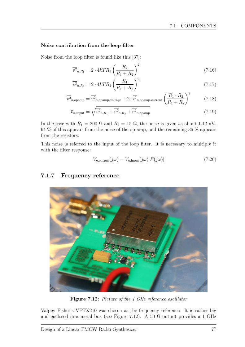
7.1. COMPONENTS
Noise contribution from the loop filter
Noise from the loop filter is found like this [37]:
v2n,R1= 2 · 4kTR1
(
R2
R1 +R2
)2
(7.16)
v2n,R2= 2 · 4kTR2
(
R1
R1 +R2
)2
(7.17)
v2n,opamp = v2n,opamp-voltage + 2 · i2n,opamp-current
(
R1 · R2
R1 +R2
)2
(7.18)
vn,input =
√
v2n,R1+ v2n,R2
+ v2n,opamp (7.19)
In the case with R1 = 200 Ω and R2 = 15 Ω, the noise is given as about 1.12 nV.64 % of this appears from the noise of the op-amp, and the remaining 36 % appearsfrom the resistors.
This noise is referred to the input of the loop filter. It is necessary to multiply itwith the filter response:
Vn,output(jω) = Vn,input(jω)|F (jω)| (7.20)
7.1.7 Frequency reference
Figure 7.12: Picture of the 1 GHz reference oscillator
Valpey Fisher’s VFTX210 was chosen as the frequency reference. It is rather bigand enclosed in a metal box (see Figure 7.12). A 50 Ω output provides a 1 GHz
Design of a Linear FMCW Radar Synthesizer 77

CHAPTER 7. CIRCUIT DESIGN
signal at a level of about +8 dBm. The DDS accepts an input of -20 to +5 dBm,so a simple T attenuator made of 3 resistors was placed between them. The PCBwas accomodated with a place for the frequency reference, but because of its highcost, it was later decided to not mount it on the board, but provide the signal via acoaxial cable from a board where it was already mounted (Figure 7.12).
7.1.8 Voltage regulator
A voltage regulator LT1963AEST-3.3 was used to provide 3.3 V to the DDS, theTCXO and the microcontroller.
7.2 Schematic
The schematic of the entire synthesizer can be seen in Figure 7.13. It was designedwith CADSTAR 12.1.
7.3 PCB
Because of the high operating frequency and the surface-mounted components, aproper PCB was needed. The design of the PCB was an important part of theconstruction. There are different materials used for PCBs. The choice was mainlybetween the Rogers laminates (RO4003 and RO4350) which are often used at higherfrequencies and the much cheaper FR-4 alternative which is used for most othertypes of circuits. Since this was a design of a 9.2 GHz frequency synthesizer, itwould probably sound smart to use a Rogers laminate. However, since a dedicatedVCO chip was used, the 9.2 GHz part of the circuit could be confined to a smallarea of the circuit board. All the critical parts were inside the VCO and only a shortline from the VCO to the output at 9.2 GHz was needed. The divide-by-4 output ofthe VCO was used to connect the VCO to the phase detector and this line carriesa signal at 2.3 GHz. The FR-4 laminate was chosen because it is cheaper and stillsuitable.
Since the AD9858 has so many pins and many of them must be connected to thepower supply, it is very useful, and pretty much compulsary, to design a multi-layerPCB. A 4-layer board was chosen. The top layer was used for the main componentsand connections. Layer 2 was used as a ground plane, layer 3 as a power plane.Different voltages were needed for the different parts of the board so by having aproper layer for the power, the voltages could neatly be distributed. The bottomlayer (layer 4) was also used as a ground plane. At places where other signals hadto cross each other, they were simply routed via either layer 3 or the bottom layerat places where the ground plane and the power plane were removed.
The entire vertical structure of the PCB is shown below.
78 Ruben Undheim

7.3. PCB
680nF
15
15
680nF
Figure 7.13: The complete schematic exported from Cadstar
Design of a Linear FMCW Radar Synthesizer 79

CHAPTER 7. CIRCUIT DESIGN
0
20
40
60
80
100
0 0.0005 0.001 0.0015 0.002 0.0025 0.003
Z0
mm
Figure 7.14: Characteristic impedance for εr = 4.2 and different widths
Blind Plated
Pri-L2 Pri-Sec
No Silkscreen
~~~~~~~~~~~~~~~~~~~~~ 20um Solder Mask
Pri ======|=======|====== 35um Copper Foil: Resistivity=1.75
XXXXX | XXXXX | XXXXX 508um FR4: Er=4.50
L2 ======|====== | ===== 35um Copper Foil: Resistivity=1.75, Embeds DOWNWARDS
XXXXXXXXXXXXX | XXXXX 483um FR4 Prepreg: Er=4.20
L3 ============= | ===== 35um Copper Foil: Resistivity=1.75, Embeds UPWARDS
XXXXXXXXXXXXX | XXXXX 508um FR4: Er=4.50
Sec ==============|====== 35um Copper Foil: Resistivity=1.75
~~~~~~~~~~~~~~~~~~~~~ 20um Solder Mask
No Silkscreen
As can be seen, two different types of vias were used. The permittivity of the FR4is 4.5 - a number that is needed when calculating line widths.
The layout was also designed with CADSTAR 12.1. For the high frequency lines -4 lines in total, the line widths must correspond to the correct line impedance. Allof them were referred to 50Ω and the engineering formula (7.22) was therefore usedto find their widths. A plot of the formula is shown in Figure 7.14 and it can beobserved that a narrower line causes a higher impedance. For this 4-layer board, theh in the formula was the distance between the top layer and layer 2, thus 508um.
εeff =εr + 1
2+
εr − 1
2√
1 + (10h/W )(7.21)
Zc =120π
√εeff(
Wh+ 1.393 + 0.667 ln
(
Wh+ 1.444
)) (7.22)
The width was found to be about 0.95 mm. An impedance calculator found on the
80 Ruben Undheim

7.3. PCB
Internet [38] was used to adjust this for the exact frequencies employed. This gave0.97 mm for the 121 MHz part, and 0.95 mm for the 9.2 GHz part.
Figure 7.15: Picture of the VCO and the output SMA connector
The SMA connectors were of the edge-mounted type (see Figure 7.15). They weredesigned for a board thickness of 1.57 mm. This was a deciding factor for that thetotal board thickness was set to this. However, the connectors are also designed forbeing attached to a microstrip line designed for this board thickness, but in thisdesign the microstrip lines are dimensioned according to the spacing between thetop layer and layer 2 (0.508 mm). A trick was done. Just at the point where thecentre conductor of the SMA connector touches the board, the microstrip was madewider (consider Figure 7.15). In addition, the copper on layer 2 and layer 3 wasremoved exactly underneath the wide part of the microstrip. By doing this, theconnector was supposed to be matched to the board. At frequencies as high as 9.2GHz, it is expected that by doing this wrongly, there will rapidly be a big loss atthe connection.
7.3.1 Finished design
The PCB layout was finished and fiducial marks were placed on the board (5 in totaleven though only 3 are stricly needed). Then the design files were exported fromCadstar. The design files consist mostly of Gerber files, but two NC drill files for thedifferent via holes and one readme file were also exported. The readme file containsimportant data about how the board was desired to be, including PCB stack-up1,board dimensions and via sizes.
1The stack-up contains the type, thickness and spacing of the different layers.
Design of a Linear FMCW Radar Synthesizer 81

CHAPTER 7. CIRCUIT DESIGN
(a) Top layer (b) Layer 2
(c) Layer 3 (d) Bottom layer
Figure 7.16: Showing the 4 different layers of the FR-4 PCB
82 Ruben Undheim
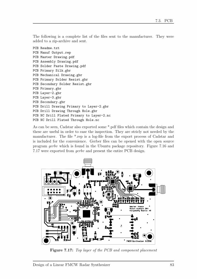
7.3. PCB
The following is a complete list of the files sent to the manufacturer. They wereadded to a zip-archive and sent.
PCB Readme.txt
PCB Manuf Output.rep
PCB Master Drawing.pdf
PCB Assembly Drawing.pdf
PCB Solder Paste Drawing.pdf
PCB Primary Silk.gbr
PCB Mechanical Drawing.gbr
PCB Primary Solder Resist.gbr
PCB Secondary Solder Resist.gbr
PCB Primary.gbr
PCB Layer-2.gbr
PCB Layer-3.gbr
PCB Secondary.gbr
PCB Drill Drawing Primary to Layer-2.gbr
PCB Drill Drawing Through Hole.gbr
PCB NC Drill Plated Primary to Layer-2.nc
PCB NC Drill Plated Through Hole.nc
As can be seen, Cadstar also exported some *.pdf files which contain the design andthese are useful in order to ease the inspection. They are stricly not needed by themanufacturer. The file *.rep is a log-file from the export process of Cadstar andis included for the convenience. Gerber files can be opened with the open sourceprogram gerbv which is found in the Ubuntu package repository. Figure 7.16 and7.17 were exported from gerbv and present the entire PCB design.
Figure 7.17: Top layer of the PCB and component placement
Design of a Linear FMCW Radar Synthesizer 83

CHAPTER 7. CIRCUIT DESIGN
Figure 7.18: Picture of the PCB without components
Figure 7.19: Close-up picture of the pads for the VCO
84 Ruben Undheim
7.4. VERIFICATION OF BOARD
7.4 Verification of Board
When the PCB arrived from the manufacturer (figure 7.18), the excitement wasgreat. All the traces were checked in order to see if they were correctly connectedinside the board. Luckily, no errors were found. Because of the components fromHittite which have soldering pads underneath, it would not be easy to solder theboard by hand. Thanks to Kongsberg Seatex, the board was sent to Simpro, Løkken,in order to be mounted. The files needed for the mounting were:
PCB Primary Assembly.gbr
PCB Primary Paste.gbr
PCB Primary Pick and Place.txt
PCB Secondary Paste.gbr
PCB BOM.xls
After a couple of days, when the board was ready, the excitement was even greater.Was it going to work?
At first, the DDS was to be checked. The board was powered up with one powersupply at 5 V. The power to the VCO and phase detector was not connected at thistime. No short-circuits were discovered, and the board was drawing the expectedcurrent of about 0.45 A. The MCU was still not programmed, so the board was notdoing anything reasonable. The AVR ISP mkII programmer was then connected be-tween the computer and the board and the code for a fixed frequency (see AppendixA.3) was used to program the microcontroller. An Agilent infiniium 54832B DSOoscilloscope was connected to the output of the DDS, and after some time fiddlingaround, the expected result appeared on the oscilloscope screen! The output was asine wave at 121.7 MHz. The DDS and MCU part of the board was thus verified,and everything worked perfectly.
Now, the next stage was to check the VCO. The output of the board was connectedto the R&S FSP spectrum analyzer and the board was powered with one supplyfor the phase detector and the VCO. What was observed on the spectrum analyzerafter carefully adjusting the frequency span and amplitude controls, was a carrierat some frequency near 8 GHz. The output signal was not very stable. Next, thepower to the op-amp was connected, 17 V. Then it was observed that the outputfrequency was changed when the op-amp voltage was adjusted.
The next stage was to be a bit more tricky. During the design, just some randomvalues for the capacitor and the resistor in the loop filter were selected. This wasdone in order to find out how important the choice is. The board was thereforenot necessarily expected to work before these components were replaced. Still, thecomplete board was powered with two different power supplies. One at 5 V for theDDS, MCU, VCO and phase detector and one at 17 V for the op-amp. The divisorof the phase detector was configured (using jumpers) to be at 19. Together with thedivision of 4 at the reference output of the VCO, the total division factor was 76.With the DDS reference frequency programmed above, the output was expected tobe 121.7 · 106 · 76 = 9.25 GHz. This was not observed. The output was not fixedat a certain frequency. It jumped around over a frequency band corresponding toa GHz or so. It was back to the calculation board. Based on the components that
Design of a Linear FMCW Radar Synthesizer 85

CHAPTER 7. CIRCUIT DESIGN
Figure 7.20: Picture of the PCB showing PLL loop and DDS
Figure 7.21: Picture of the complete circuit
86 Ruben Undheim

7.4. VERIFICATION OF BOARD
were on the board, the natural frequency of the board was found to be 630 kHz andthe damping factor 1.8. These values were consequently not good. According to thesimulations performed earlier, the best natural frequency should be about 30 kHz,and the best damping factor about 1.0 (see Figure 6.11 and 6.12 page 63). Newcomponents values were calculated to be C1 = 470nF and R2 = 22 Ω. However,these exact values were not selected because they were not available at the moment.The capacitors were changed to 100 nF and the resistors to 15 Ω. After they werereplaced, the board was once again powered. The expected natural frequency was tobe 63 kHz, and the expected damping factor, ζ , was to be 1.11. These values weremuch closer to the calculated ideal values, and the board was this time thereforeexpected to work.
And it was working! By tuning the spectrum analyzer to 9.25 GHz, it was observedthat the output was remarkably stable. The lock had been achieved. It was kind ofa surprise. There had not been so much trouble getting it to work than feared, andall the worries could be abandonded.
Design of a Linear FMCW Radar Synthesizer 87

88
Chapter 8
Measurements
8.1 Equipment
These are all the instruments that were used for the measurements.
• Tektronix RSA6114A Real-Time Spectrum Analyzer
• Rohde & Schwarz FSP Spectrum Analyzer 9 kHz .. 13.6 Ghz
• Rohde & Schwarz FSQ 40 Signal Analyzer 20 Hz .. 40 GHz
• Anritsu MS2724C Spectrum Analyzer 9 kHz .. 20 GHz
• Agilent infiniium 54832B DSO 1 GHz 1GSa/s Oscilloscope
• Anritsu MG3691B Signal Generator 10GHz
• Topward Dual-Tracking DC Power Supply 6303D
• Rohde & Schwarz NRP-Z21 AVG Power Sensor
8.2 Procedure
At first, the frequency and level of the output signal were measured since all theother measurements depend on them. The level was measured using the NRP-Z21power sensor. With the loop filter components set to C1 = 100 nF, and R2 = 15 Ω,the output spectrum was measured with the R&S FSP spectrum analyzer using aspan of 800 kHz and a resolution bandwidth (RBW) of 3 kHz. Then C1 was changedto 680 nF in order to get nearer the good values calculated in Section 7.4. R2 waskept at 15 Ω and the output was once again measured.
8.2.1 Phase Noise
Then the phase noise measurements were performed. The spectrum analyzer fromAnritsu was used most of the time, but a few tests were also done with the R&S
89

CHAPTER 8. MEASUREMENTS
FSQ40 which has a built-in phase-noise measurement option. By using this option,the other measurements could be verified. The Anritsu spectrum analyzer is portableand does not have a very good phase noise performance itself which may be limiting.
Figure 8.1: The capacitors and resistors of the loop filter that were changed (How itlooked like after about 30 changes). Note that the two capacitors have the same valueand are referred to as C1 while the resistors have the same value and are referred toas R2
The span of the spectrum analyzer was set to 200 kHz in order to see the mostimportant part of the phase noise spectrum. Both of the sidebands were observedeven though they are expected to be equal to each other (when there is no amplitudenoise). Thus, the phase noise was measured from zero to 100 kHz offset. After everymeasurement, R2 was changed and a new measurement was performed. C1 was keptat 680 nF. The measurements were performed with the RBW set to 10 Hz and theVBW set to 3 Hz.
Afterwards, the effect of different capacitor values was tested. C1 was changed from680 nF to 470 nF with R2 equal 22 Ω. Then, R2 was set to 10 Ω and the samecapacitor change was done once again (figure 9.5).
Since it was not certain if the measurements performed were correct because ofpossibly wrong scaling and related issues, the dedicated phase noise option of theFSQ spectrum analyzer was used to do a control check. The phase noise performanceof this instrument is much better and it will therefore not obscure the measurements.It also measures at higher offset frequencies and plots with a logarithmic frequencyaxis. The loop filter values used in this case were C1 = 680 nF and R2 = 33 Ω.Because of this, it is possible to compare the result directly with the calculatedphase noise in Section 6.2. The phase noise measurement option is pretty muchautomatic, only the carrier frequency and level must be entered before pushing theRUN-button.
90 Ruben Undheim

8.2. PROCEDURE
Figure 8.2: Picture of the board during testing. Notice the green LED in the centerwhich indicates that the PLL is in lock.
8.2.2 Step Response
Because of the access to a real-time spectrum analyzer, some really interesting mea-surements could be performed. This type of spectrum analyzer works differentlyfrom other spectrum analyzers by first sampling the signal and then calculating thespectrum from the samples. It is therefore capable of showing frequency changessuch as a plot of frequency vs time. This can then be used in order to find thebandwidth and the damping factor of the PLL.
The microcontroller was for the step-response measurements programmed with theswitch-frequency program (Section A.4). The frequency is switched rapidly between9.200 GHz and 9.208 GHz. This is accomplished by programming the DDS with twodifferent profiles and then switching between them with the set profile() function.The spectrum analyzer was set to trigger at a frequency of about 9.204 GHz andthe frequency span was set to ±10 MHz.
Figure 8.3 is a screenshot from the instrument. Time is on the x-axis, and frequencyis on the y-axis. It shows how a typical frequency step looks like.
8.2.3 Sweep
The last thing tested was sweeping. The code for the sweep (Appendix A.5) was pro-grammed into the microcontroller, and the real-time spectrum analyzer was config-ured for a frequency span of ±20 MHz. Since the spectrum analyzer performs better
Design of a Linear FMCW Radar Synthesizer 91

CHAPTER 8. MEASUREMENTS
Figure 8.3: Typical response of a frequency step observed on a real-time spectrumanalyzer. Note that time is along the x-axis, and frequency is along the y-axis.
with narrower spans, it was decided to just let the synthesizer sweep a bandwidthof 25 MHz and not 100 MHz which the operative radar will. It was programmed tosweep from 9.250 to 9.275 GHz. The DFTW register in the DDS was set to 1000which from equation (7.7) corresponds to a step size of
∆f =DFTW × SY SCLK
232= 233Hz
at the reference frequency, or 17.7 kHz at the operating frequency. The time betweenevery step was set to 8 µs by setting DFRRW also to 1000 (7.8). About
25 MHz
17.7 kHz· 8µs = 12 ms
was then needed to sweep 25 MHz. The sweep rate was 2.21 GHz per second - fairlyhigh.
A symmetrical sweep was also tested. The sweep rate was doubled (DFTW = 2000)to get both the up-sweep and the down-sweep on the same screen using the samescaling as for the asymmetrical sweep. The delay of the microcontroller had tobe decreased correspondingly. In order to make a symmetrical sweep, the sweepdirection manually had to be changed when the output had reached its maximumfrequency. The microcontroller therefore had to time exactly how long the sweepneeded. To make the sweep always start from the same frequency for the up-sweep,and another frequency for the down-sweep, the frequency incrementer was reset andthe start frequency manually configured after each sweep.
92 Ruben Undheim

Chapter 9
Results
-70
-60
-50
-40
-30
-20
-10
0
10
20
9.2496 9.2497 9.2498 9.2499 9.25 9.2501 9.2502 9.2503
dB
m
GHz
Figure 9.1: The signal observed scaled in dBm. C1 = 100 nF, R2 = 56 Ω, RBW:3 kHz, VBW: 100 Hz
The initial results were of the frequency and the level. The frequency was found tobe 9.249963 GHz - very close to 9.25 GHz as expected from the DDS settings. Usingthe power sensor, the level was found to be about +11 dBm. By varying the VCOvoltage from 4.5 V to 5.5 V, the output level varied from +9.95 dBm to +11.75dBm. According to the datasheet (Appendix E.1), it was supposed to be between+10 and +15 dBm so it seemed to be fine. The spectrum of the signal is presentedin Figure 9.1 and 9.2 with a span 800 kHz, a resolution bandwidth 3 kHz and a videobandwidth 100 Hz. It should be noted that because of the resolution bandwidth,the noise seen will not correspond to noise power per Hz. If this is desired, it mustfirst be scaled by a factor as explained in Section 3.6. Also, the noise floor is caused
93

CHAPTER 9. RESULTS
-70
-60
-50
-40
-30
-20
-10
0
10
20
9.2496 9.2497 9.2498 9.2499 9.25 9.2501 9.2502 9.2503
dB
m
GHz
Figure 9.2: The signal observed scaled in dBm. C1 = 680 nF, R2 = 15 Ω, RBW:3 kHz, VBW: 100 Hz
by thermal noise in the instrument and is therefore not part of the signal. Figure 9.1presents the measurement with a bandwidth, fn, of 63kHz and a damping factor,ζ , of 1.11. fn is much higher than what was predicted to be the best. The skirt ofphase noise is therefore clearly visible and quite bad. It can be noted that the noisepower increases somewhat at increasing offsets near the carrier before decreasingagain. Some peaks are visible at about 100 kHz offset, and obviously the main peak(the carrier) is visible in the center. The level of the carrier can be observed atabout +11 dBm which is the same as what was measured with the power meter.Figure 9.2 presents the same output when the loop filter components are changed.It should correspond to a bandwidth of 24 MHz and a damping factor of 0.7. Theskirt of phase noise has been reduced a lot. It may still be seen that the amplitudeincreases somewhat at increasing offsets, before decreasing again.
9.1 Phase Noise
Different resistance values R2 in the loop filter
The first phase noise measurements are presented in Figure 9.3. It shows the phasenoise for offset frequencies between 0 and 100 kHz on both sides of the carrier. Thecapacitor values in the loop filter are fixed at 680 nF which should correspond to abandwidth of 24 kHz. The resistor values have been varied from 10 Ω to 62 Ω whichshould correspond to a damping factor from 0.15 to 3.2. All the plots for phasenoise are scaled according to the noise bandwidth and the signal level and therefore
94 Ruben Undheim

9.1. PHASE NOISE
-110
-105
-100
-95
-90
-85
-80
-75
9.24988 9.24992 9.24996 9.25 9.25004
dB
c/H
z
GHz
R = 10
18
22
33
47
62
Figure 9.3: Phase noise with different damping factors. Span 200 kHz.
present the results in dBc/Hz.
It is noted that when the resistor value is small, there is a visible increase of phasenoise at offsets a bit away from the carrier. The maximum is seen at about 19 kHzfor the 10 Ω resistor value and at about 35 kHz for the 33 Ω resistor. For resistancevalues of 47 Ω and higher, there is no such clear increase of phase noise.
The phase noise is in general lower near the carrier for the higher resistor values.At higher offsets, which are near the edge of the plot, the opposite is the case. Thehigher the resistance is, the more constant the phase noise spectrum seems to be.Undesired spikes are observed at 62 kHz for all of them and at 32 kHz offset for the18 Ω case. These are most likely caused by spurs.
Different capacitor values in the loop filter
The spectra for different capacitor values with a fixed resistor value of 22 Ω arepresented in Figure 9.4. The two capacitor values used are 470 nF and 680 nF.470nF should give the bandwidth 29 kHz and 680 nF, 24 kHz. The span is in thiscase also 200 kHz so that it allows the phase noise for offset frequencies up to 100kHz to be seen. An increase of the phase noise at higher offsets is observed whichwould be expected as the previous measurement also indicates such an increase withresistor values below 47 Ω. The noise decreases again at offsets higher than 32 kHz.Maximum noise is about -90 dBc/Hz at 32 kHz offset for both of them. It is slightlyhigher for 680 nF. The spikes at 62 kHz are seen in both cases.
With 470 nF, lower phase noise at offsets below 50 kHz is observed. At greateroffsets, the phase noise is more or less the same.
Design of a Linear FMCW Radar Synthesizer 95
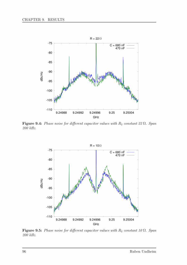
CHAPTER 9. RESULTS
-110
-105
-100
-95
-90
-85
-80
-75
9.24988 9.24992 9.24996 9.25 9.25004
dB
c/H
z
GHz
R = 22
C = 680 nF
470 nF
Figure 9.4: Phase noise for different capacitor values with R2 constant 22 Ω. Span200 kHz.
-110
-105
-100
-95
-90
-85
-80
-75
9.24988 9.24992 9.24996 9.25 9.25004
dB
c/H
z
GHz
R = 10
C = 680 nF
470 nF
Figure 9.5: Phase noise for different capacitor values with R2 constant 10 Ω. Span200 kHz.
96 Ruben Undheim

9.1. PHASE NOISE
In Figure 9.5, the result from the measurement with R2 = 10 Ω is presented. Thecapacitor is also in this case varied between 470 nF and 680 nF. It can be observedthat for offsets below 19 kHz, the noise is lower with C1 = 470 nF, while for offsetsbetween 19 kHz and 62 kHz, the noise is lower with C1 = 680 nF. There is a clearpeaking of about -84 dBc/Hz at 23.5 kHz for C1 = 470 nF and of about -87 dBc/Hz at20.5 kHz for C1 = 680 nF. This is much higher than for the previous measurements.The spurs at 62 kHz are still there.
Phase noise option in the R&S FSQ spectrum analyzer
The measurements performed with the phase noise option (Figure 9.6) reveils thatthe phase noise found and scaled earlier is correct. The expected bandwidth is 24kHz and the expected damping factor 1.7. It also includes the phase noise at offsetsup to 1 MHz. The results are presented with a logarithmic frequency axis and theplot can therefore more or less be compared directly with the predictions in Section6.2.
It can be noted that the noise remains quite constant from 1 kHz offset to 20-30kHz offset, before it starts decreasing at a relatively constant rate (logaritmically)from 30 kHz to the edge of the plot. There is a little peak at about 230 kHz, butthe spike observed earlier at 62 kHz is gone.
Many more measurements of the phase noise were performed, but only some wereselected to be presented here.
-140
-130
-120
-110
-100
-90
103
104
105
106
dB
c/H
z
Hz
Figure 9.6: Phase noise measured with phase noise option on FSQ. The capacitorvalues are here 680 nF and the resistor values 33 Ω.
Design of a Linear FMCW Radar Synthesizer 97

CHAPTER 9. RESULTS
9.2 Frequency Step
Figure 9.7: Response of a frequency step observed on a real-time spectrum analyzer,R2 = 10 Ω, C1 = 470 nF. Frequency vs time
Capacitance Resistance Bandwidth Damping470 nF 10 Ω 23 kHz 0.22470 nF 22 Ω 24 kHz 0.55470 nF 33 Ω 24 kHz 0.8680 nF 10 Ω 19.5 kHz 0.31680 nF 22 Ω 19.5 kHz 0.67680 nF 33 Ω 19.5 kHz 1.01
Table 9.1: Measured bandwidth and damping factors for different values of C andR
A screenshot of the frequency step response measurement is shown in Figure 9.7.Thereis clearly a ringing response which indicates that the damping factor is somewhattoo low. For this measurement, the bandwidth was expected to be 29 kHz and thedamping factor 0.43.
Plots of the measurements with different resistor values are presented in Figure 9.8.It can be observed that with a higher resistor value, the ringing disappears. At 22Ω there is still a small tendency to ringing, while at 33 Ω there is just one singleovershoot before the frequency settles.
The same measurements with another capacitor value are presented in Figure 9.9.What is observed, is more or less the same as in the previous figure, but the response
98 Ruben Undheim

9.2. FREQUENCY STEP
-4e+06
-2e+06
0
2e+06
4e+06
6e+06
0.00010.000150.00020.000250.00030.000350.00040.000450.00050.000550.0006
time (s)
-4e+06
-2e+06
0
2e+06
4e+06
6e+06
0.00010.000150.00020.000250.00030.000350.00040.000450.00050.000550.0006
time (s)
-4e+06
-2e+06
0
2e+06
4e+06
6e+06
0.00010.000150.00020.000250.00030.000350.00040.000450.00050.000550.0006
time (s)
Figure 9.8: Responses of frequency steps observed on a real-time spectrum analyzer.C1 = 470 nF. For three different values of R2 - 10 Ω, 22 Ω and 33 Ω
Design of a Linear FMCW Radar Synthesizer 99

CHAPTER 9. RESULTS
is slightly more damped. In addition, it is noticed that the ringing is slower - thefrequency is lower.
From all these responses, the bandwidth and damping factor could be found. Itwas done by fitting curves from the expressions in Section 4.4 page 41 with themeasurements. The result is presented in table 9.1
-4e+06
-2e+06
0
2e+06
4e+06
6e+06
0.00010.000150.00020.000250.00030.000350.00040.000450.00050.000550.0006
time (s)
-4e+06
-2e+06
0
2e+06
4e+06
6e+06
0.00010.000150.00020.000250.00030.000350.00040.000450.00050.000550.0006
time (s)
-4e+06
-2e+06
0
2e+06
4e+06
6e+06
0.00010.000150.00020.000250.00030.000350.00040.000450.00050.000550.0006
time (s)
Figure 9.9: Responses of frequency steps observed on a real-time spectrum analyzer,C1 = 680 nF. For three different values of R2 - 10 Ω, 22 Ω and 33 Ω
9.3 Sweep
Asymmetrical sweep
The result of the asymmetrical sweep can be seen in Figure 9.10. Note the littledelay after each return-to-start before it starts sweeping again. The delay lasts for1.7 ms. The sweep all in all lasts for 11.88 ms. Also note the overshoot when thefrequency switches back to the start frequency. The sweep bandwidth is 26.9 MHzand the overshoot when returning is 3.2 MHz, 12 % of the total sweep bandwidth.The capacitor value C1 used here was 680 nF and the resistor R2, 33 Ω.
100 Ruben Undheim
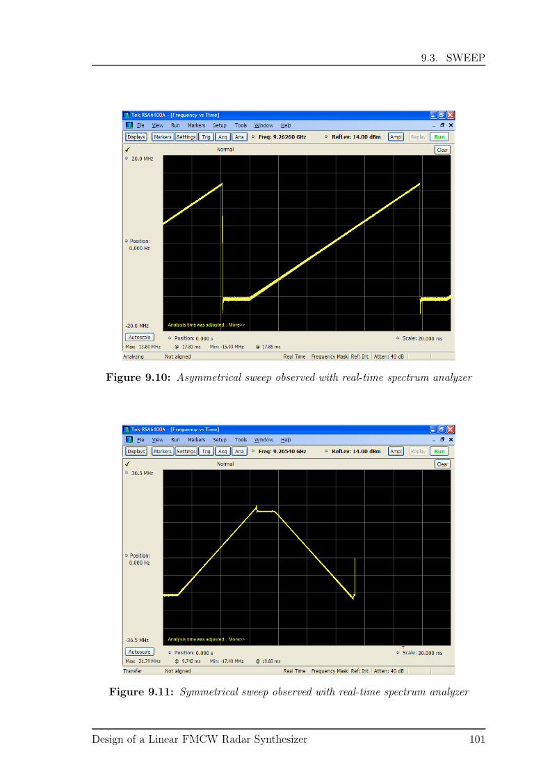
9.3. SWEEP
Figure 9.10: Asymmetrical sweep observed with real-time spectrum analyzer
Figure 9.11: Symmetrical sweep observed with real-time spectrum analyzer
Design of a Linear FMCW Radar Synthesizer 101

CHAPTER 9. RESULTS
Symmetrical sweep
Since the return rate and start frequency have to be set manually by the MCU,the first attempt to make a symmetrical sweep ended up like Figure 9.11 presents.The up-sweep reaches a higher frequency than the one set for the beginning of thedown-sweep. It therefore looks a bit ugly. The new frequency was adjusted slightlyand new tests were performed. In Figure 9.12, the problem is gone. The maximumfrequency is however slightly higher than for the previous case.
Figure 9.12: Symmetrical sweep observed with real-time spectrum analyzer
102 Ruben Undheim
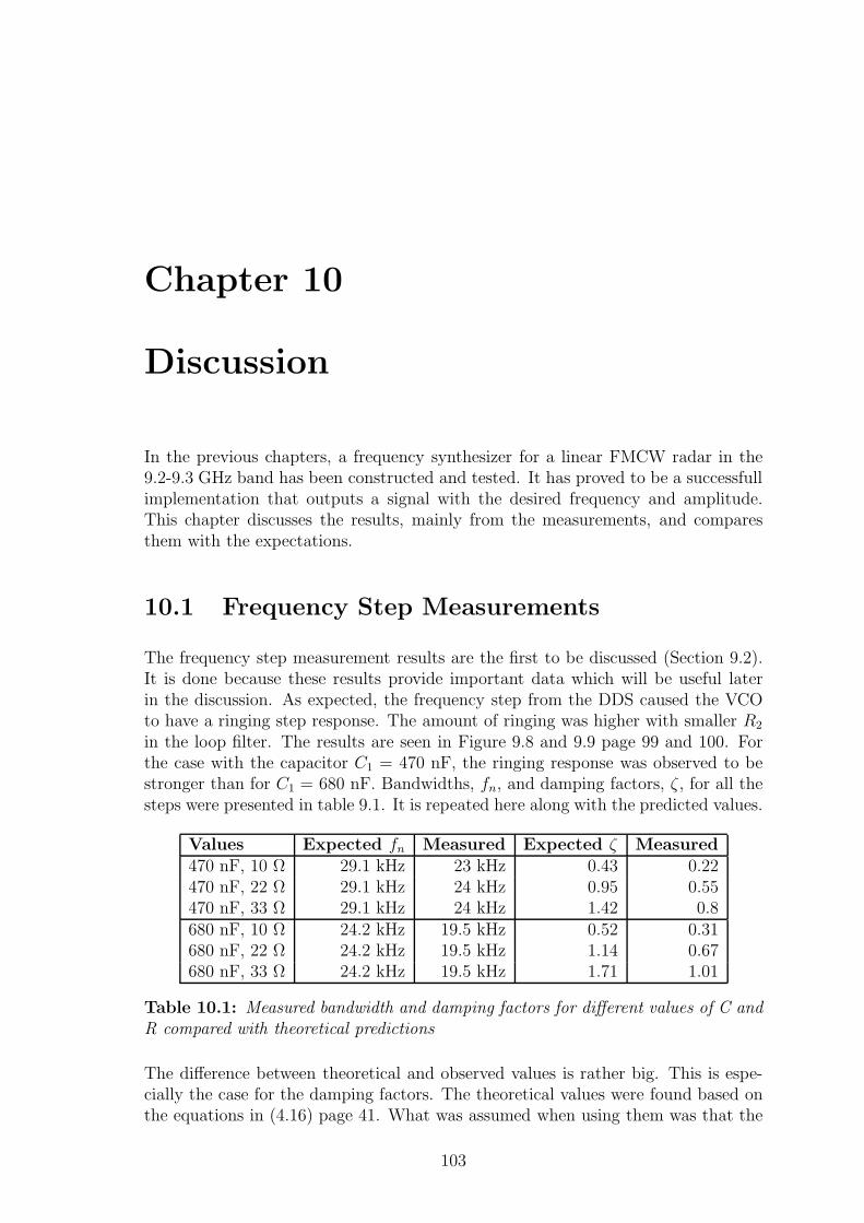
Chapter 10
Discussion
In the previous chapters, a frequency synthesizer for a linear FMCW radar in the9.2-9.3 GHz band has been constructed and tested. It has proved to be a successfullimplementation that outputs a signal with the desired frequency and amplitude.This chapter discusses the results, mainly from the measurements, and comparesthem with the expectations.
10.1 Frequency Step Measurements
The frequency step measurement results are the first to be discussed (Section 9.2).It is done because these results provide important data which will be useful laterin the discussion. As expected, the frequency step from the DDS caused the VCOto have a ringing step response. The amount of ringing was higher with smaller R2
in the loop filter. The results are seen in Figure 9.8 and 9.9 page 99 and 100. Forthe case with the capacitor C1 = 470 nF, the ringing response was observed to bestronger than for C1 = 680 nF. Bandwidths, fn, and damping factors, ζ , for all thesteps were presented in table 9.1. It is repeated here along with the predicted values.
Values Expected fn Measured Expected ζ Measured470 nF, 10 Ω 29.1 kHz 23 kHz 0.43 0.22470 nF, 22 Ω 29.1 kHz 24 kHz 0.95 0.55470 nF, 33 Ω 29.1 kHz 24 kHz 1.42 0.8680 nF, 10 Ω 24.2 kHz 19.5 kHz 0.52 0.31680 nF, 22 Ω 24.2 kHz 19.5 kHz 1.14 0.67680 nF, 33 Ω 24.2 kHz 19.5 kHz 1.71 1.01
Table 10.1: Measured bandwidth and damping factors for different values of C andR compared with theoretical predictions
The difference between theoretical and observed values is rather big. This is espe-cially the case for the damping factors. The theoretical values were found based onthe equations in (4.16) page 41. What was assumed when using them was that the
103
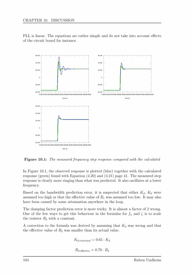
CHAPTER 10. DISCUSSION
PLL is linear. The equations are rather simple and do not take into account effectsof the circuit board for instance.
-4e+06
-2e+06
0
2e+06
4e+06
6e+06
0.00010.000150.00020.000250.00030.000350.00040.000450.00050.000550.0006
time (s)
-4e+06
-2e+06
0
2e+06
4e+06
6e+06
0.00010.000150.00020.000250.00030.000350.00040.000450.00050.000550.0006
time (s)
-4e+06
-2e+06
0
2e+06
4e+06
6e+06
0.00010.000150.00020.000250.00030.000350.00040.000450.00050.000550.0006
time (s)
Figure 10.1: The measured frequency step response compared with the calculated
In Figure 10.1, the observed response is plotted (blue) together with the calculatedresponse (green) found with Equation (4.20) and (4.21) page 41. The measured stepresponse is clearly more ringing than what was predicted. It also oscillates at a lowerfrequency.
Based on the bandwidth prediction error, it is suspected that either Kd, K0 wereassumed too high or that the effective value of R1 was assumed too low. It may alsohave been caused by some attenuation anywhere in the loop.
The damping factor prediction error is more tricky. It is almost a factor of 2 wrong.One of the few ways to get this behaviour in the formulas for fn and ζ is to scalethe resistor R2 with a constant.
A correction to the formula was derived by assuming that Kd was wrong and thatthe effective value of R2 was smaller than its actual value.
Kd-corrected = 0.65 ·Kd
R2-effective = 0.70 · R2
104 Ruben Undheim

10.1. FREQUENCY STEP MEASUREMENTS
fn =1
2π
√
Kd-correctedK0
NR1Cζ =
R2-effective
2
√
CKd-correctedK0
NR1
(10.1)
That R2-effective is smaller than R2 can be caused by multiple factors. First of all,the loop filter is not perfect. The loop filter receives pulses at a rate of 121 MHz,and the actual design may create capacitors that reduce the effective resistance(impedance). It is also possible that the configuration is not symmetric enoughand hence the asymmetry will play a role. The op-amp has been powered with asingle voltage supply and not a double-voltage which it usually is. This in itself maylead to changes in the behaviour. The PLL is considered linear in the calculations.Perhaps its nonlinearities play such a big role that they cause big deviations. Thisshould however not cause a systematic error like here for multiple values of ζ . Thefrequency step is quite small (8 MHz at the operating frequency, 91 kHz at the phasedetector frequency), and it should be expected that the PLL operates in its linearregion. Note that all this is speculation. It is also possible, under doubt, that theprediction error simply is caused by calculation errors.
-4e+06
-2e+06
0
2e+06
4e+06
6e+06
0.00010.000150.00020.000250.00030.000350.00040.000450.00050.000550.0006
time (s)
-4e+06
-2e+06
0
2e+06
4e+06
6e+06
0.00010.000150.00020.000250.00030.000350.00040.000450.00050.000550.0006
time (s)
-4e+06
-2e+06
0
2e+06
4e+06
6e+06
0.00010.000150.00020.000250.00030.000350.00040.000450.00050.000550.0006
time (s)
-4e+06
-2e+06
0
2e+06
4e+06
6e+06
0.00010.000150.00020.000250.00030.000350.00040.000450.00050.000550.0006
time (s)
Figure 10.2: The measured frequency step response compared with predictions withcorrected formula for C = 470 nF (upper two) and C = 680 nF (lower two)
However, even though the absolute values of fn and ζ do not correspond directly tothe calculated values, the trend certainly matches the theory. It is clearly observed
Design of a Linear FMCW Radar Synthesizer 105

CHAPTER 10. DISCUSSION
that by increasing the resistance, the response becomes more damped, while increas-ing the capacitance gives a lower ringing frequency. By employing the correctionformula developed above, the measured values are again compared with calculatedvalues for several different values of C1 and R2. The results are plotted in Figure10.2. It can be observed that the formula fits very well. The trend has thereforebeen verified.
10.2 Phase Noise Measurements
The effect on the phase noise of changing the resistor value (Figure 9.3 page 95)corresponds well to theory. When the resistor value R2 increases, and hence also ζ ,the phase noise spectrum becomes more and more flat. It corresponds well with thepredictions made in Chapter 6.
What is not so good, is that the absolute level of the phase noise is considerablyhigher than predicted. It was expected to see it around -105 dBc/Hz at its best,but instead it is at about -97 dBc/Hz. One thing that should be noted is that theAnritsu Spectrum analyzer has such a high phase noise, that for the measurementswith the highest resistor values, the measurements are most likely influenced by theinstrument phase noise. In addition, the bandwidth and damping factors used whenpredicting the phase noise were in the previous section shown to be wrong.
-140
-130
-120
-110
-100
-90
103
104
105
106
dB
c/H
z
Hz
Measured phase noiseCalculated phase noise
Calculated phase noise with wrong fn and ζ
Figure 10.3: The measured phase noise compared with the expected
The result from the phase noise option in the FSQ spectrum analyzer is not so easilyobscured by instrumentation phase noise. It is compared with calculated values in
106 Ruben Undheim

10.2. PHASE NOISE MEASUREMENTS
Offset Estimated Measured Difference(dBc/Hz) (dBc/Hz) (dBc/Hz)
1 kHz −99.6 −93.5 +6.110 kHz −102.4 −93.0 +9.4100 kHz −112.3 −107.3 +5.11 MHz −132.3 −135.8 −3.5
Table 10.2: The measured phase noise compared with the estimation
-140
-130
-120
-110
-100
-90
103
104
105
106
dB
c/H
z
Hz
Figure 10.4: Excessive noise in the loop filter will cause such a behaviour
Design of a Linear FMCW Radar Synthesizer 107

CHAPTER 10. DISCUSSION
Figure 10.3. Two different predictions are plotted. Here the reward of first findingthe real PLL bandwidth using frequency step testing is seen (Section 10.1). Thered curve is based on fn and ζ first predicted, while the green curve is based on thenew values for fn and ζ found by analyzing the step response. It can be seen thatthere is quite a lot more phase noise than calculated. It is however readily seen thatthe green curve fits the measured phase noise better than the red curve. It startsdecreasing at about the same offset.
Table 10.2 summarizes the deviation between predicted values (with correct band-with and damping factor) and the measured value. It is observed that at low offsets,the prediction is better than achieved, but at offsets approaching 1 MHz, the mea-surements are slightly better. It is not good that there is so much more phase noisethan expected. It should be noted however, that the calculated phase noise mostlycorresponds to the best obtainable phase noise. This may seem strange since thephase noise at high offsets got better. The last may be caused by the fact that thelow-pass filter following the loop filter (Figure 7.11 page 75) was not included whenthe predictions of the phase noise were made.
In order to try to find out what could cause the additional phase noise, new calcu-lations were done. By adding 14 dB to the phase noise of the loop filter at offset upto 500 kHz, decreasing the noise slightly at 1 MHz and above, as well as adding 10dB to the noise from the reference, a new plot was made.
The result is seen in Figure 10.4. The curve seems to fit well. Based on thisdiscovery, it might be suspected that the main problem is noise from the loop filter.By holding a screwdriver against a metal point in the loop filter, it was observedthat the phase noise could easily be increased 20-30 dB more. It is therefore obviousthat what happens regarding noise in the loop filter can be extremely devastatingfor the performance.
Different things were attempted in order to find the cause. It was suspected that thepower supply could play a role. Figure 10.5 shows what happened when differentparts of the board were powered with independent power supplies and also whenthe power to the op-amp was powered by a battery with short cables. Only onesideband is shown. The result shows that there was not much to be gained by usingbatteries for the op-amp, but by separating the supply for the VCO from the DDS,the phase noise was actually improved quite much. This just illustrates the factthat the noise may come via the supply voltage or more likely propagate via thesupply voltage wiring. One error had probably been made during the design. Everysubsection of the board should have had its own low noise voltage regulator withseveral capacitors of different sizes. Apparently, a power plane and some capacitorsdid not suffice. Unfortunately, there was not any time left to try this out. There wasonly time for one attempt of making a synthesizer. It should however be appreciatedthat it at least worked - in spite of the phase noise not being optimal.
108 Ruben Undheim

10.3. FREQUENCY SWEEP MEASUREMENTS
-110
-105
-100
-95
-90
-85
-80
-75
-70
9.25 9.25005 9.2501 9.25015
dB
c/H
z
GHz
With Power SupplyOn battery
Separate VCO/DDS SupplyBetter Supply Cables
Figure 10.5: Testing the effect of changing power supplies
10.3 Frequency Sweep Measurements
The frequency sweep measurements did not reveal so many surprises. The outputswept where it was told to sweep. One thing that can be noted is that since thesweep type employed for the measurements was short, the time the microcontrollerneeded in order to send the control commands to the DDS was a significant part ofthe period. First of all this caused the delays at the top and bottom of the sweep.Two commands had to be sent for resetting the frequency incrementer. For thecase with symmetrical sweep, a new frequency also had to be set at the end of eachsweep. Because the AD9858 buffers the instructions and first make them active aftera toggle on the FUD pin, most of the commands could be sent during the sweep.This obviously caused the microcontroller to not have to wait for such a long time.Almost 2 ms was needed in order to send one command, and for the symmetricalsweep, the sleeping time of the micocontroller had to be set to the total sweep timeminus the time for two commands, 4 ms. The slow control commands are a resultof that the microcontroller runs at a frequency of 1 MHz. The DDS is capable ofreceiving instructions at a rate of 10 MHz [29]. The clock divider that is enabledby default inside the ATtiny2313 transforms an internal 8 MHz oscillator into a 1MHz clock signal. This divider could easily be disabled by a fuse setting, and thecommand delay would then be 8 times as short.
Another possibility is to run the microcontroller from an external oscillator. Thiswas not included in the design because it slightly complicates it more. The SYSCLKoutput of the AD9858 could have been divided down and used as the clock oscillatorto get 10 MHz. In that case, the microcontroller would have been synchronized
Design of a Linear FMCW Radar Synthesizer 109
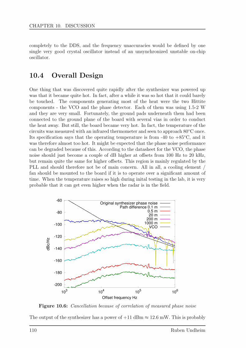
CHAPTER 10. DISCUSSION
completely to the DDS, and the frequency unaccuracies would be defined by onesingle very good crystal oscillator instead of an unsynchronized unstable on-chiposcillator.
10.4 Overall Design
One thing that was discovered quite rapidly after the synthesizer was powered upwas that it became quite hot. In fact, after a while it was so hot that it could barelybe touched. The components generating most of the heat were the two Hittitecomponents - the VCO and the phase detector. Each of them was using 1.5-2 Wand they are very small. Fortunately, the ground pads underneath them had beenconnected to the ground plane of the board with several vias in order to conductthe heat away. But still, the board became very hot. In fact, the temperature of thecircuits was measured with an infrared thermometer and seen to approach 80C once.Its specification says that the operating temperature is from -40 to +85C, and itwas therefore almost too hot. It might be expected that the phase noise performancecan be degraded because of this. According to the datasheet for the VCO, the phasenoise should just become a couple of dB higher at offsets from 100 Hz to 20 kHz,but remain quite the same for higher offsets. This region is mainly regulated by thePLL and should therefore not be of main concern. All in all, a cooling element /fan should be mounted to the board if it is to operate over a significant amount oftime. When the temperature raises so high during inital testing in the lab, it is veryprobable that it can get even higher when the radar is in the field.
-200
-180
-160
-140
-120
-100
-80
-60
103
104
105
106
dB
c/H
z
Offset frequency Hz
Original synthesizer phase noisePath difference 0.1 m
0.5 m20 m
200 m1000 m
VCO
Figure 10.6: Cancellation because of correlation of measured phase noise
The output of the synthesizer has a power of +11 dBm ≈ 12.6 mW. This is probably
110 Ruben Undheim
10.4. OVERALL DESIGN
not enough to be connected directly to the antenna. In order to have a functionalradar, an output level in the range of a few watts would be better. Therefore apower amplifier will be needed. This has not been considered in this design, butan amplifier with a gain of about 20 dB would be desired. Its main requirement isobviously that it should not add much phase noise.
The cancellation factor from Chapter 5 was used to calculate the effective radarphase noise for the measured phase noise spectrum of the frequency synthesizerexactly as was done earlier for the open-loop VCO. The result is presented in figure10.6 for several different path lengths differences. The effective phase noise can bemade very low and for very short path lengths, it will fall below the thermal noisefloor. The phase noise of the open-loop VCO is included in the plot too.
Design of a Linear FMCW Radar Synthesizer 111

112
Chapter 11
Conclusion
In this thesis, there has been a focus on radars, phase noise and PLLs. In addition,a frequency synthesizer in the X-band at 9.2-9.3 GHz has been designed, built andtested. Generally speaking, the results are good. The functionality of the circuitis successful. However, the absolute magnitude of the phase noise is higher thanpredicted. It has been shown that this can be caused by many factors, but themost likely source is excessive noise in the loop filter of the PLL possibly causedby unstable supply voltage. To tweak the last dB’s away from the phase noise,especially care must be taken during the design. All the critical components shouldhave their own low-noise voltage regulators to provide reliable supply voltages.
While working with the thesis, a great amount of knowledge has been acquired in amultitude of different disciplines of electronics engineering. The work has providedexperience in PCB design, programming, soldering and spectrum analyzing. Phasenoise appears as a comprehensive subject to the author. After studying it for awhile, there are still new things and new aspects of it that show up, but in general,everything is now much clearer than before. Understanding how the phase noisespectrum relates to the signal spectrum was especially interesting. An ideal carrierhas infinite power at a single frequency, but the phase noise ensures that the signalis realistic and distributes its power over a finite bandwidth. Seeing how phase noisegets canceled because of correlation effects, was another interesting thing. It alsohas several potential uses. The perhaps most triggering thing was that the circuitthat was designed and built worked very well. Unfortunately, there was not timeenough to test it so extensively that the direct cause of the phase noise predictionerror could be established.
It has been a fun time. Trying out new things and learning new things are alwaysfun. But at the same time, it has been stressful. A lot had to be done to arrive here.
11.1 Future Work
As a future project, a power amplifier should be built, so that the synthesizer can beused in practice. The radar receiver must also be implemented. Since the transmitted
113
CHAPTER 11. CONCLUSION
signal is also used as the local oscillator of the receiver, the output can be split to thepower amplifier and the receiver. An interesting project may also be to implementthe digital signal processing on an FPGA. An FFT processor is the main component.
Regarding the synthesizer designed here, it would be interesting to find out thedirect cause of the failure to exactly predict the bandwidth and damping of thePLL. Spending some extra time finding out why there was more phase noise thanpredicted, is perhaps neither a bad idea.
114 Ruben Undheim

List of Figures
2.1 How marine vessels can use radars. In this case a pulse radar. . . . . 32.2 Principle of basic pulse radar . . . . . . . . . . . . . . . . . . . . . . 42.3 One pulse in frequency domain . . . . . . . . . . . . . . . . . . . . . 52.4 Many pulses in frequency domain . . . . . . . . . . . . . . . . . . . . 62.5 How Pulse-Doppler signal processing can be performed . . . . . . . . 72.6 How an asymmetrical linear sweep FMCW radar sweeps . . . . . . . 92.7 How a symmetrical linear sweep FMCW radar sweeps . . . . . . . . . 92.8 Conceptual diagram of an FMCW Radar . . . . . . . . . . . . . . . . 112.9 Conceptual diagram of FMCW Radar with complex processing . . . . 12
3.1 Thermal noise of resistors . . . . . . . . . . . . . . . . . . . . . . . . 183.2 Evolution of circuit noise into phase noise . . . . . . . . . . . . . . . 193.3 How the signal spectrum is related to the phase spectrum . . . . . . . 213.4 Carrier with added noise in a 1 Hz bandwidth . . . . . . . . . . . . . 233.5 Leeson’s equation . . . . . . . . . . . . . . . . . . . . . . . . . . . . . 253.6 Evolution of circuit noise into phase noise . . . . . . . . . . . . . . . 263.7 Impulse response of LC tank . . . . . . . . . . . . . . . . . . . . . . . 27
4.1 Block diagram of PLL . . . . . . . . . . . . . . . . . . . . . . . . . . 354.2 Mathematical block diagram of PLL . . . . . . . . . . . . . . . . . . 364.3 A basic PFD . . . . . . . . . . . . . . . . . . . . . . . . . . . . . . . 384.4 Showing 3 common types of loop filters . . . . . . . . . . . . . . . . . 394.5 Frequency step with a PLL bandwidth of 14kHz . . . . . . . . . . . . 424.6 Frequency step with a PLL bandwidth of 4kHz . . . . . . . . . . . . 424.7 How the PLL will modify the phase noise of a VCO . . . . . . . . . . 44
5.1 How targets can be masked by the phase noise . . . . . . . . . . . . . 455.2 Cancellation effect of phase noise because of correlation . . . . . . . . 475.3 Beat signal when using unquantized sweep . . . . . . . . . . . . . . . 485.4 Beat signal when using big steps . . . . . . . . . . . . . . . . . . . . . 495.5 Beat signal when using smaller steps . . . . . . . . . . . . . . . . . . 505.6 How the step rate influences the spectrum of the beat signal . . . . . 505.7 Beat signal when using practical steps . . . . . . . . . . . . . . . . . 51
6.1 Simple illustration of the concept for generating a sweep . . . . . . . 536.2 A sweep generator using a PLL with variable prescaler . . . . . . . . 546.3 Using a DDS as the reference to the PLL . . . . . . . . . . . . . . . . 55
115

LIST OF FIGURES
6.4 Equal to the previous one just with a frequency doubler at the output. 566.5 PLL having frequency conversion in the loop. . . . . . . . . . . . . . 566.6 Predicted phase noise for the topology with frequency conversion in
the loop and an ideal oscillator . . . . . . . . . . . . . . . . . . . . . 576.7 Predicted phase noise for the topology with frequency conversion in
the loop with an oscillator with equal phase noise performance as theTCXO . . . . . . . . . . . . . . . . . . . . . . . . . . . . . . . . . . . 58
6.8 Predicted phase noise for the topology with frequency conversion inthe loop with an oscillator 20 dB worse than the TCXO . . . . . . . . 58
6.9 Direct mixing of the DDS signal with a fixed frequency oscillator. . . 596.10 Predicted phase noise for different phase detector frequencies . . . . 626.11 Predicted phase noise for different loop bandwidths . . . . . . . . . . 636.12 Predicted phase noise for different damping factors . . . . . . . . . . 646.13 Bode diagram of the open loop response of the PLL . . . . . . . . . . 656.14 Bode diagram of the closed loop response of the PLL . . . . . . . . . 66
7.1 Block diagram of the design . . . . . . . . . . . . . . . . . . . . . . . 677.2 Connections of the VCO (HMC510) . . . . . . . . . . . . . . . . . . . 687.3 Picture of the DDS . . . . . . . . . . . . . . . . . . . . . . . . . . . . 697.4 Two baluns . . . . . . . . . . . . . . . . . . . . . . . . . . . . . . . . 707.5 How the DDS was connected . . . . . . . . . . . . . . . . . . . . . . . 707.6 How the registers in the DDS controls the automatic sweep . . . . . . 727.7 Filter to remove image products from the DDS output . . . . . . . . 737.8 Response of the low-pass filter . . . . . . . . . . . . . . . . . . . . . . 737.9 Pinout of AVR ATtiny2313 [33] . . . . . . . . . . . . . . . . . . . . . 747.10 How the galvanic isolation was achieved with an optocoupler . . . . . 747.11 Schematic of the loop-filter . . . . . . . . . . . . . . . . . . . . . . . . 757.12 Picture of the 1 GHz reference oscillator . . . . . . . . . . . . . . . . 777.13 The complete schematic exported from Cadstar . . . . . . . . . . . . 797.14 Characteristic impedance for εr = 4.2 and different widths . . . . . . 807.15 Picture of the VCO and the output SMA connector . . . . . . . . . . 817.16 Showing the 4 different layers of the FR-4 PCB . . . . . . . . . . . . 827.17 Top layer of the PCB and component placement . . . . . . . . . . . . 837.18 Picture of the PCB without components . . . . . . . . . . . . . . . . 847.19 Close-up picture of the pads for the VCO . . . . . . . . . . . . . . . . 847.20 Picture of the PCB showing PLL loop and DDS . . . . . . . . . . . . 867.21 Picture of the complete circuit . . . . . . . . . . . . . . . . . . . . . . 86
8.1 The capacitors and resistors of the loop filter that were changed. . . . 908.2 Picture of the board during testing . . . . . . . . . . . . . . . . . . . 918.3 Typical response of a frequency step observed on a real-time spectrum
analyzer . . . . . . . . . . . . . . . . . . . . . . . . . . . . . . . . . . 92
9.1 The signal observed scaled in dBm. C1 = 100 nF, R2 = 56 Ω, RBW:3 kHz, VBW: 100 Hz . . . . . . . . . . . . . . . . . . . . . . . . . . . 93
9.2 The signal observed scaled in dBm. C1 = 680 nF, R2 = 15 Ω, RBW:3 kHz, VBW: 100 Hz . . . . . . . . . . . . . . . . . . . . . . . . . . . 94
116 Ruben Undheim
LIST OF FIGURES
9.3 Phase noise with different damping factors . . . . . . . . . . . . . . . 959.4 Phase noise for different capacitor values, C1, with R2 constant 22 Ω . 969.5 Phase noise for different capacitor values with R2 constant 10 Ω . . . 969.6 Phase noise measured with phase noise option on FSQ . . . . . . . . 979.7 Response of a frequency step observed on a real-time spectrum ana-
lyzer, R2 = 10 Ω, C1 = 470 nF. . . . . . . . . . . . . . . . . . . . . . 989.8 Responses of frequency steps observed on a real-time spectrum ana-
lyzer. C1 = 470 nF. For three different values of R2 - 10 Ω, 22 Ω and33 Ω . . . . . . . . . . . . . . . . . . . . . . . . . . . . . . . . . . . . 99
9.9 Responses of frequency steps observed on a real-time spectrum ana-lyzer, C1 = 680 nF. For three different values of R2 - 10 Ω, 22 Ω and33 Ω . . . . . . . . . . . . . . . . . . . . . . . . . . . . . . . . . . . . 100
9.10 Asymmetrical sweep observed with real-time spectrum analyzer . . . 1019.11 Symmetrical sweep observed with real-time spectrum analyzer . . . . 1019.12 Symmetrical sweep observed with real-time spectrum analyzer . . . . 102
10.1 The measured frequency step response compared with the calculated 10410.2 The measured frequency step response compared with predictions
with corrected formula for C = 470 nF (upper two) and C = 680nF (lower two) . . . . . . . . . . . . . . . . . . . . . . . . . . . . . . 105
10.3 The measured phase noise compared with the expected . . . . . . . . 10610.4 Excessive noise in the loop filter will cause such a behaviour . . . . . 10710.5 Testing the effect of changing power supplies . . . . . . . . . . . . . . 10910.6 Cancellation because of correlation of measured phase noise . . . . . 110
B.1 How to connect series resistors for ISP programming . . . . . . . . . 131
D.1 Output of DDS with images . . . . . . . . . . . . . . . . . . . . . . . 145D.2 Output of DDS with images . . . . . . . . . . . . . . . . . . . . . . . 146
Design of a Linear FMCW Radar Synthesizer 117

118
Bibliography
[1] A.G. Stove. Linear fmcw radar techniques. Radar and Signal Processing, IEEProceedings F, 139(5):343 –350, oct 1992.
[2] D.B. Leeson. A simple model of feedback oscillator noise spectrum. Proceedingsof the IEEE, 54(2):329 – 330, feb. 1966.
[3] A. Hajimiri and T.H. Lee. A general theory of phase noise in electrical oscilla-tors. Solid-State Circuits, IEEE Journal of, 33(2):179 –194, feb 1998.
[4] A. Demir, A. Mehrotra, and J. Roychowdhury. Phase noise in oscillators: a uni-fying theory and numerical methods for characterization. Circuits and SystemsI: Fundamental Theory and Applications, IEEE Transactions on, 47(5):655 –674, may 2000.
[5] David K. Barton. Radars - CW and Doppler Radar. Artech House, 1980.
[6] Merrill I. Skolnik. Introduction to Radar Systems. McGraw-Hill, 3rd edition,2001.
[7] Merrill I. Skolnik. Radar Handbook. McGraw-Hill, 2nd edition, 1990.
[8] W. Holm and J. Echard. Fft signal processing for non-coherent radar systems.In Acoustics, Speech, and Signal Processing, IEEE International Conference onICASSP ’82., volume 7, pages 363 – 366, may 1982.
[9] Ole K. Nilsen and W. D. Boyer. Amplitude modulated cw radar. Aerospace andNavigational Electronics, IRE Transactions on, ANE-9(4):250 –254, dec. 1962.
[10] Bill Mullarkey. The differences between pulse radars and fmcw ones. Navigate-us.com, dec 2008.
[11] Igor V. Komarov and Sergey M. Smolskiy. Fundamentals of Short-Range FMRadar. Artech House, 2003.
[12] United States Department of Commerce. United states frequency allocationschart 2011 - the radio spectrum. http://commons.wikimedia.org/wiki/File:United States Frequency Allocations Chart 2011 -The Radio Spectrum.pdf, 2011.
[13] E.S. Ferre-Pikal, J.R. Vig, J.C. Camparo, L.S. Cutler, L. Maleki, W.J. Riley,S.R. Stein, C. Thomas, F.L. Walls, and J.D. White. Draft revision of ieee std1139-1988 standard definitions of physical quantities for fundamental, frequency
119

BIBLIOGRAPHY
and time metrology-random instabilities. In Frequency Control Symposium,1997., Proceedings of the 1997 IEEE International, pages 338 –357, may 1997.
[14] Michal Odyniec. RF and Microwave Oscillator Design. Artech House, 2002.
[15] W.P. Robins. Phase Noise in Signal Sources. Peter Peregrinus Ltd, 1982.
[16] Karl Rottmann. Matematisk Formelsamling. Spektrum forlag, 11th edition,2003.
[17] Floyd M. Gardner. Phaselock Techniques. Wiley-Interscience, 3rd edition, 2004.
[18] T.H. Lee and A. Hajimiri. Oscillator phase noise: a tutorial. Solid-State Cir-cuits, IEEE Journal of, 35(3):326 –336, mar 2000.
[19] G.J. Coram. A simple 2-d oscillator to determine the correct decompositionof perturbations into amplitude and phase noise. Circuits and Systems I: Fun-damental Theory and Applications, IEEE Transactions on, 48(7):896 –898, jul2001.
[20] Mike Curtin and Paul O’Brien. Phase-locked loops for high-frequency receiversand transmitters - part 2. Analog Dialogue by Analog Devices, 1999.
[21] David Owen. Good practice to phase noise measurement. Pickering Interfaces,(68), 2004.
[22] J.I. Brown. A digital phase and frequency-sensitive detector. Proceedings of theIEEE, 59(4):717 – 718, april 1971.
[23] Floyd M. Gardner. Charge-pump phase-lock loops. Communications, IEEETransactions on, 28(11):1849 – 1858, nov 1980.
[24] Jr. M.C. Budge and M.P. Burt. Range correlation effects in radars. In RadarConference, 1993., Record of the 1993 IEEE National, pages 212 –216, 1993.
[25] M. Pichler, A. Stelzer, P. Gulden, and M. Vossiek. Influence of systematicfrequency-sweep non-linearity on object distance estimation in fmcw/fscw radarsystems. In Microwave Conference, 2003. 33rd European, volume 3, pages 1203– 1206 Vol.3, oct. 2003.
[26] G.M. Brooker. Understanding millimetre wave fmcw radars. 1st InternationalConference on Sensing Technology, Nov. 2005.
[27] Hittite Microwave Corporation. HMC510LP5 Datasheet.
[28] Valpey Fisher Corporation. VFTX210 Datasheet.
[29] Analog Devices. AD9858 Datasheet.
[30] Ken Gentile. Driving a center-tapped transfomer with a balanced current-output dac. Analog Devices - Application Note AN-912.
[31] Analog Devices. Ad9858 evaluation board.http://www.analog.com/en/evaluation/EVAL-AD9858/eb.html.
[32] Dale Heatherington. Design an l-c low pass or high pass filter.http://www.wa4dsy.net/filter/hp lp filter.html, May 2008.
120 Ruben Undheim

BIBLIOGRAPHY
[33] Atmel. AVR ATtiny2313 Datasheet.
[34] Hittite Microwave Corporation. HMC698LP5 Datasheet.
[35] Peter White. Understanding phase noise from digital components in pll fre-quency synthesizers. Applied Radio Labs, DN006, dec. 2000.
[36] T.J. Endres and J.B. Kirkpatrick. Sensitivity of fast settling plls to differentialloop filter component variations. In Frequency Control Symposium, 1992. 46th.,Proceedings of the 1992 IEEE, pages 213 –224, may 1992.
[37] Analog Devices. ADA4898-1 Datasheet rev C, 2010.
[38] Microstrip line calculator. http://www1.sphere.ne.jp/i-lab/ilab/tool/ms line e.htm.
[39] Atmel. In-system programming. Application Note, AVR910, 2008.
[40] Analog Devices. A technical tutorial on digital signal synthesis. 1st Interna-tional Conference on Sensing Technology, 1999.
Design of a Linear FMCW Radar Synthesizer 121

122
Appendix A
Source Code ATtiny2313
A.1 ad9858control.h
1 /*
2 Software for ATtiny2313 on
3 FMCW Synthesizer 9.2GHz board
4
5 by
6 Ruben Undheim
7 Master thesis 2012 NTNU
8 */
9
10 # ifndef INC_AD9858_H
11 # define INC_AD9858_H
12
13 # include <avr / io.h>
14 # include <avr / interrupt.h>
15 # include <util / delay.h>
16
17 # define DDS_PS0 _BV(PD2)
18 # define DDS_PS1 _BV(PD3)
19 # define DDS_FUD _BV(PD4)
20 # define DDS_RESET _BV(PD5)
21 # define DDS_CS _BV(PD6) //inverted!!!
22
23 # define DDS_SCLK _BV(PB0)
24 # define DDS_SDIO _BV(PB1)
25 # define DDS_SDO _BV(PB2)
26 # define DDS_IORESET _BV(PB3)
27
28 # define CTRL_PWRDOWN 2
29 # define CTRL_2GHZ 6
30 # define CTRL_PWRMIX 4
31 # define CTRL_PWRPD 3
32 # define CTRL_SWEEP 15
33 # define CTRL_CLRFREQ 20
34 # define CTRL_AUTOCLR 23
35
36 # define ACTIVE
37 # define DELAYBIT 1000
38 // Clear:
39 // PORTB &= ~DDS_SCLK;
40 // Set:
41 // PORTB |= DDS_SCLK;
42
43 // bits transferred at rising SCLK edge
123

APPENDIX A. SOURCE CODE ATTINY2313
44 // reading transferred on falling edge of SCLK
45 // LSB first
46
47 void delay_ms(uint16_t ms);
48 void delay_mini(uint16_t mini);
49 void send_byte(uint8_t byte);
50 void write_short(uint8_t address, uint16_t data);
51 void write_long(uint8_t address, uint32_t data);
52 uint32_t read_long(uint8_t address);
53 void ioreset(void);
54 void init(void);
55 void selectchip(uint8_t truefalse);
56 uint8_t receive_byte(void);
57 void set_control(uint32_t long_word);
58 void set_default(void);
59 void set_bit(uint8_t bitnr, uint8_t active);
60 void toggle_fud(void);
61 void set_profile(uint8_t profile);
62
63 extern uint32_t control_reg;
64
65 # endif /* INC_AD9858_H */
A.2 ad9858control.c
1 /*
2 Software for ATtiny2313 on
3 FMCW Synthesizer 9.2GHz board
4
5 by
6 Ruben Undheim
7 Master thesis 2012 NTNU
8 */
9 # define F_CPU 1000000UL
10
11 # include "ad9858control.h"
12
13 uint32_t control_reg;
14
15 void delay_ms(uint16_t ms)
16 while ( ms )
17
18 _delay_ms(1);
19 ms--;
20
21
22 void delay_mini(uint16_t mini)
23 while ( mini )
24
25 asm("nop");
26 mini--;
27
28
29 void send_byte(uint8_t byte)
30 uint8_t active;
31 uint8_t i;
32 for(i=0;i<8;i++)
33 active = (0x01 & (byte >> (7-i)));
34 if(active == 1)
35 PORTB |= DDS_SDIO;
36
37 else if(active == 0)
124 Ruben Undheim

A.2. AD9858CONTROL.C
38 PORTB &= ~DDS_SDIO;
39
40 PORTB |= DDS_SCLK;
41 PORTB &= ~DDS_SCLK;
42
43
44
45 uint8_t receive_byte(void)
46 uint8_t received = 0x00;
47 uint8_t active = 0x00;
48 uint8_t i;
49 for(i=0;i<8;i++)
50 delay_ms(1);
51 PORTB |= DDS_SCLK;
52 delay_ms(1);
53 active = ((PINB & DDS_SDIO) != 0);
54 PORTB &= ~DDS_SCLK;
55 delay_ms(1);
56 received &= (active << (7-i));
57
58 return received;
59
60 void write_short(uint8_t address, uint16_t data)
61 DDRB |= DDS_SDIO;
62 address &= ~0x80;
63 # ifdef ACTIVE
64 selectchip(1);
65 # endif
66 send_byte(address);
67
68 send_byte((uint8_t)((data >> 8) & 0xFF));
69 send_byte((uint8_t)((data) & 0xFF));
70
71 # ifdef ACTIVE
72 selectchip(0);
73 # endif
74
75 void write_long(uint8_t address, uint32_t data)
76 DDRB |= DDS_SDIO;
77 address &= ~0x80;
78 # ifdef ACTIVE
79 selectchip(1);
80 # endif
81 send_byte(address);
82
83 send_byte((uint8_t)((data >> 24) & 0xFF));
84 send_byte((uint8_t)((data >> 16) & 0xFF));
85 send_byte((uint8_t)((data >> 8) & 0xFF));
86 send_byte((uint8_t)((data) & 0xFF));
87
88 # ifdef ACTIVE
89 selectchip(0);
90 # endif
91
92 uint32_t read_long(uint8_t address)
93 uint32_t read = 0x00;
94 DDRB |= DDS_SDIO; // write read command
95 address |= 0x80;
96 # ifdef ACTIVE
97 selectchip(1);
98 # endif
99
100 send_byte(address);
101
102 DDRB &= ~DDS_SDIO; // start reading
103 PORTB &= ~DDS_SDIO;
104 read |= (((uint32_t)receive_byte() << 24) & 0xFF000000);
105 read |= (((uint32_t)receive_byte() << 16) & 0x00FF0000);
106 read |= (((uint32_t)receive_byte() << 8) & 0x0000FF00);
107 read |= ((uint32_t)receive_byte() & 0x000000FF);
Design of a Linear FMCW Radar Synthesizer 125
APPENDIX A. SOURCE CODE ATTINY2313
108
109 # ifdef ACTIVE
110 selectchip(0);
111 # endif
112 return read;
113
114
115 void selectchip(uint8_t truefalse)
116 if(truefalse == 1)
117 PORTD &= ~DDS_CS;
118 else if(truefalse == 0)
119 PORTD |= DDS_CS;
120
121
122 void ioreset()
123 PORTB |= DDS_IORESET;
124 delay_ms(1);
125 PORTB &= ~DDS_IORESET;
126 delay_ms(1);
127
128
129
130 void set_bit(uint8_t bitnr, uint8_t active)
131 uint32_t mask = ((uint32_t)0x00000001) << (bitnr);
132 if(active == 1)
133 set_control((control_reg | mask));
134 else
135 set_control((control_reg & ~mask));
136
137
138 void set_control(uint32_t long_word)
139 write_long(0x00,long_word);
140 control_reg = long_word;
141
142
143 void set_default(void)
144 set_control(0x00000018);
145
146
147 void set_profile(uint8_t profile)
148 if(profile == 1)
149 PORTD = (PORTD & ~DDS_PS0) & ~DDS_PS1;
150
151 else if(profile == 2)
152 PORTD = (PORTD | DDS_PS0) & ~DDS_PS1;
153
154 else if(profile == 3)
155 PORTD = (PORTD & ~DDS_PS0) | DDS_PS1;
156
157 else if(profile == 4)
158 PORTD = (PORTD | DDS_PS0) | DDS_PS1;
159
160
161
162 void toggle_fud(void)
163 PORTD |= DDS_FUD;
164 PORTD &= ~DDS_FUD;
165
166
167 void init()
168 control_reg = 0x00000018;
169 DDRB = 0x0f ; /* Enable output on all the port B pins */
170 DDRB &= ~DDS_SDO;
171 DDRD = 0xfe ; /* Enable output on all the port B pins */
172 PORTB = 0x00 ; /* Set them to 0 */
173 PORTD = 0x00;
174 PORTD |= DDS_CS;
175 delay_ms(100);
176 ioreset();
177
126 Ruben Undheim

A.3. MAIN-FIXEDFREQUENCY.C
A.3 main-fixedfrequency.c
1 /*
2 Software for ATtiny2313 on
3 FMCW Synthesizer 9.2GHz board
4
5 by
6 Ruben Undheim
7 Master thesis 2012 NTNU
8 */
9 # define F_CPU 1000000UL
10 # define N 13
11 # include <avr / io.h>
12 # include <avr / interrupt.h>
13 # include <util / delay.h>
14 # include "ad9858control.h"
15
16
17 int main(void)
18 init();
19
20 /* Divisor 19 */
21 //uint32_t fvalue = 37796000; // very low
22
23 //uint32_t fvalue = 463400000; // 8.2GHz
24 //----uint32_t fvalue = 4.8036e8; // 8.5GHz
25 //----uint32_t fvalue = 4.9731e8; // 8.8GHz
26 //uint32_t fvalue = 5.1427e8; // 9.1GHz
27 //uint32_t fvalue = 5.1992e8; // 9.2GHz
28 uint32_t fvalue = 5.2274e8; // 9.25GHz
29 //uint32_t fvalue = 5.2557e8; // 9.3GHz
30 //uint32_t fvalue = 5.3122e8; // 9.4GHz
31 //----uint32_t fvalue = 536870912; // 9.5GHz
32 //----uint32_t fvalue = 5.4817e8; // 9.7GHz
33 //uint32_t fvalue = 5.5382e8; // 9.8GHz
34
35
36 /* Divisor 13 */
37 //uint32_t fvalue = 7.0207e8; // 8.5
38 //uint32_t fvalue = 7.1859e8; // 8.7
39 //uint32_t fvalue = 6.7729e8; // 8.2
40 //uint32_t fvalue = 7.51625e8; // 9.1
41 //uint32_t fvalue = 7.5988e8; // 9.2
42 //uint32_t fvalue = 7.6401e8; // 9.25
43 //uint32_t fvalue = 7.6814e8; // 9.3
44 //uint32_t fvalue = 7.764e8; // 9.4
45 //uint32_t fvalue = 8.0944e8; // 9.8
46
47 delay_ms(500);
48 set_bit(CTRL_2GHZ,1);
49 toggle_fud();
50 write_long(0x03,fvalue);
51 set_profile(1);
52 toggle_fud();
53
54
Design of a Linear FMCW Radar Synthesizer 127

APPENDIX A. SOURCE CODE ATTINY2313
A.4 main-switchfreq.c
1 /*
2 Software for ATtiny2313 on
3 FMCW Synthesizer 9.2GHz board
4
5 by
6 Ruben Undheim
7 Master thesis 2012 NTNU
8 */
9 # define F_CPU 1000000UL
10 # include <avr / io.h>
11 # include <avr / interrupt.h>
12 # include <util / delay.h>
13 # include "ad9858control.h"
14
15
16 int main(void)
17 init();
18 uint32_t fvalue = 5.1992e8; // 9.2GHz
19 uint32_t fvalue2 = 5.2025e8;
20
21
22 delay_ms(500);
23 set_bit(CTRL_2GHZ,1);
24 toggle_fud();
25 write_long(0x03,fvalue);
26 write_long(0x05,fvalue2);
27 toggle_fud();
28 while(1)
29 set_profile(1);
30 delay_mini(120);
31 set_profile(2);
32 delay_mini(120);
33
34
35
A.5 main-sweeper.c
1 /*
2 Software for ATtiny2313 on
3 FMCW Synthesizer 9.2GHz board
4
5 by
6 Ruben Undheim
7 Master thesis 2012 NTNU
8 */
9
10 # define F_CPU 1000000UL
11 # include <avr / io.h>
12 # include <avr / interrupt.h>
13 # include <util / delay.h>
14 # include "ad9858control.h"
15
16
17 int main(void)
18 init();
19 uint32_t fvalue = 5.2274e8; // 9.25GHz
20 # define DFTW 1000
128 Ruben Undheim
A.6. MAIN-SYMSWEEPER.C
21 # define DFRRW 1000
22 delay_ms(500);
23 set_bit(CTRL_2GHZ,1);
24
25 toggle_fud();
26 write_long(0x03,fvalue);
27 toggle_fud();
28 set_bit(CTRL_SWEEP,1);
29 toggle_fud();
30 write_long(0x01,DFTW); // frequency step size
31 write_short(0x02,DFRRW); // how much time
32 toggle_fud();
33
34 while(1)
35 toggle_fud();
36 set_bit(CTRL_CLRFREQ,0);
37 toggle_fud();
38 set_bit(CTRL_CLRFREQ,1);
39 //delay_ms(45*speed/step);
40 delay_ms(10);
41
42
43
44
A.6 main-symsweeper.c
1 /*
2 Software for ATtiny2313 on
3 FMCW Synthesizer 9.2GHz board
4
5 by
6 Ruben Undheim
7 Master thesis 2012 NTNU
8 */
9
10 # define F_CPU 1000000UL
11 # include <avr / io.h>
12 # include <avr / interrupt.h>
13 # include <util / delay.h>
14 # include "ad9858control.h"
15
16
17 int main(void)
18 init();
19 uint32_t fvalue = 5.2274e8; // 9.25GHz
20 uint32_t fvalue2 = 5.2480e8; // 9.25GHz
21 # define DFTW 2000
22 # define tid 1000
23 delay_ms(500);
24 set_bit(CTRL_2GHZ,1);
25
26 toggle_fud();
27 write_long(0x03,fvalue);
28 toggle_fud();
29 set_bit(CTRL_SWEEP,1);
30 toggle_fud();
31 write_long(0x01,DFTW);
32 write_short(0x02,tid);
33 toggle_fud();
34
35 while(1)
Design of a Linear FMCW Radar Synthesizer 129

APPENDIX A. SOURCE CODE ATTINY2313
36 toggle_fud();
37 set_bit(CTRL_CLRFREQ,0);
38 toggle_fud();
39 set_bit(CTRL_CLRFREQ,1);
40 write_long(0x03,fvalue2);
41 write_long(0x01,-DFTW); // Turn direction
42 delay_ms(3);
43 toggle_fud();
44 set_bit(CTRL_CLRFREQ,0);
45 toggle_fud();
46 set_bit(CTRL_CLRFREQ,1);
47 write_long(0x03,fvalue);
48 write_long(0x01,DFTW);
49 delay_ms(3);
50
51
52
53
130 Ruben Undheim

Appendix B
In-System Programming (ISP) ofAVR
To make it possible to program the microcontroller on the board, certain consid-erations must be made [39]. There are 6 pins of the AVR that are used whenprogramming:
• VCC
• RESET
• MISO
• MOSI
• SCK
• GND
The initialization of the programming is performed by pulling RESET low. The 3communication pins MISO, MOSI and SCK are often used for other purposes thanprogramming. Series resistors should be added between them and what they areconnected to in order to avoid driver contention (see Figure B.1).
Figure B.1: How to connect series resistor for ISP programming. [39]
The circuit is by default not powered via the ISP, but the VCC connection is usedto monitor the voltage. Power must therefore be applied externally to the circuit.
131

APPENDIX B. IN-SYSTEM PROGRAMMING (ISP) OF AVR
All in all, a connector with 6 pins is needed. This is then used to connect the AtmelAVR ISP mkII Programmer to the board.
132 Ruben Undheim

Appendix C
Source Code Octave
C.1 phasenoise-doall.m
1 %
2 % Master thesis
3 % Ruben Undheim 2012
4 %
5
6 %phasenoise(350e6);
7 [f,pn132_1] = phasenoise1(121e6,2*pi*30e3,0.70);
8 %set(0,"Defaulttextfontsize",32)
9 [f,pn132_2] = phasenoise1(121e6,2*pi*30e3,0.1);
10 [f,pn132_3] = phasenoise1(121e6,2*pi*30e3,0.4);
11 [f,pn132_4] = phasenoise1(121e6,2*pi*30e3,1.0);
12 [f,pn132_5] = phasenoise1(121e6,2*pi*30e3,2.0);
13 [f,pn132_6] = phasenoise1(121e6,2*pi*30e3,5.0);
14 [f,pn132_7] = phasenoise1(121e6,2*pi*30e3,10);
15 %[f,pn132_2] = phasenoise2(132e6,2*pi*100e3,0.707,5e9);
16 %phasenoise(50e6);
17
18 figure(1)
19
20 set(gca,’fontsize’,32)
21 semilogx(f,pn132_1,’linewidth’,5,f,pn132_2,’linewidth’,5,...
22 f,pn132_3,’linewidth’,5,f,pn132_4,’linewidth’,5,...
23 f,pn132_5,’linewidth’,5,f,pn132_6,’linewidth’,5,...
24 f,pn132_7,’linewidth’,5);%,f,refuti,’linewidth’,2,f,loopvcouti,’linewidth’,2);
25 title(’PLL Bandwidth 30kHz, PD Freq 121MHz’);
26 xlabel(’Offset frequency Hz’);
27 ylabel(’Phase noise dBc/Hz’);
28 legend(’\zeta = 0.7’,’0.1’,’0.4’,’1.0’,’2.0’,’5.0’,’10.0’);
29
30 print -color -deps -F:32 ../thesis/figur/phasenoisesimul-dampfactor.eps
31
32 [f,pn132_1] = phasenoise1(121e6,2*pi*0e3,0.70);
33 [f,pn132_2] = phasenoise1(121e6,2*pi*5e3,0.7);
34 [f,pn132_3] = phasenoise1(121e6,2*pi*15e3,0.7);
35 [f,pn132_4] = phasenoise1(121e6,2*pi*30e3,0.7);
36 [f,pn132_5] = phasenoise1(121e6,2*pi*50e3,0.7);
37 [f,pn132_6] = phasenoise1(121e6,2*pi*80e3,0.7);
38 [f,pn132_7] = phasenoise1(121e6,2*pi*100e3,0.7);
39
40 figure(2)
41 set(gca,’fontsize’,32)
42 semilogx(f,pn132_1,’linewidth’,5,f,pn132_2,’linewidth’,5,...
43 f,pn132_3,’linewidth’,5,f,pn132_4,’linewidth’,5,...
133

APPENDIX C. SOURCE CODE OCTAVE
44 f,pn132_5,’linewidth’,5,f,pn132_6,’linewidth’,5,...
45 f,pn132_7,’linewidth’,5 );%,f,refuti,’linewidth’,2,f,loopvcouti,’linewidth’,2);
46 title(’PLL Damping factor constant 0.7, PD Freq 121MHz’);
47 xlabel(’Offset frequency Hz’);
48 ylabel(’Phase noise dBc/Hz’);
49 legend(’f_n = 0 kHz’,’5 kHz’,’15 kHz’,’30 kHz’,’50 kHz’,’80 kHz’,’100 kHz’);
50
51 print -color -deps -F:32 ../thesis/figur/phasenoisesimul-bandwidth.eps
52
53 [f,pn132_1] = phasenoise1(121e6,2*pi*30e3,0.7);
54 [f,pn132_2] = phasenoise2(121e6,2*pi*30e3,0.7,2e9);
55 [f,pn132_3] = phasenoise2(121e6,2*pi*30e3,0.7,4e9);
56 [f,pn132_4] = phasenoise2(121e6,2*pi*30e3,0.7,6e9);
57 [f,pn132_5] = phasenoise2(121e6,2*pi*30e3,0.7,9e9);
58
59 figure(3)
60 set(gca,’fontsize’,32)
61 semilogx(f,pn132_1,’linewidth’,5,f,pn132_2,’linewidth’,5,...
62 f,pn132_3,’linewidth’,5,f,pn132_4,’linewidth’,5,...
63 f,pn132_5,’linewidth’,5)
64 title(’PLL Bandwidth 30kHz, PD Freq 121MHz’);
65 xlabel(’Offset frequency Hz’);
66 ylabel(’Phase noise dBc/Hz’);
67 legend(’No frequency conversion’,’f_LO = 2 GHz’,’4 GHz’,’6 GHz’,’9 GHz’);
68
69 print -color -deps -F:32 ../thesis/figur/phasenoisesimul-mix.eps
70
71
72 [f,pn132_1] = phasenoise1(121e6,2*pi*30e3,0.7);
73 [f,pn132_2] = phasenoise3(121e6,2*pi*30e3,0.7,2e9);
74 [f,pn132_3] = phasenoise3(121e6,2*pi*30e3,0.7,4e9);
75 [f,pn132_4] = phasenoise3(121e6,2*pi*30e3,0.7,6e9);
76 [f,pn132_5] = phasenoise3(121e6,2*pi*30e3,0.7,9e9);
77
78 figure(4)
79 set(gca,’fontsize’,32)
80 semilogx(f,pn132_1,’linewidth’,5,f,pn132_2,’linewidth’,5,...
81 f,pn132_3,’linewidth’,5,f,pn132_4,’linewidth’,5,...
82 f,pn132_5,’linewidth’,5)
83 title(’PLL Bandwidth 30kHz, PD Freq 121MHz’);
84 xlabel(’Offset frequency Hz’);
85 ylabel(’Phase noise dBc/Hz’);
86 legend(’No frequency conversion’,’f_LO = 2 GHz’,’4 GHz’,’6 GHz’,’9 GHz’);
87
88 print -color -deps -F:32 ../thesis/figur/phasenoisesimul-mix2.eps
89
90
91 [f,pn132_1] = phasenoise1(121e6,2*pi*30e3,0.7);
92 [f,pn132_2] = phasenoise4(121e6,2*pi*30e3,0.7,2e9);
93 [f,pn132_3] = phasenoise4(121e6,2*pi*30e3,0.7,4e9);
94 [f,pn132_4] = phasenoise4(121e6,2*pi*30e3,0.7,6e9);
95 [f,pn132_5] = phasenoise4(121e6,2*pi*30e3,0.7,9e9);
96
97 figure(5)
98 set(gca,’fontsize’,32)
99 semilogx(f,pn132_1,’linewidth’,5,f,pn132_2,’linewidth’,5,...
100 f,pn132_3,’linewidth’,5,f,pn132_4,’linewidth’,5,...
101 f,pn132_5,’linewidth’,5)
102 title(’PLL Bandwidth 30kHz, PD Freq 121MHz’);
103 xlabel(’Offset frequency Hz’);
104 ylabel(’Phase noise dBc/Hz’);
105 legend(’No frequency conversion’,’f_LO = 2 GHz’,’4 GHz’,’6 GHz’,’9 GHz’);
106
107 print -color -deps -F:32 ../thesis/figur/phasenoisesimul-mix3.eps
108
109 [f,pn132_1] = phasenoise1(50e6,2*pi*30e3,0.7);
110 [f,pn132_2] = phasenoise1(82e6,2*pi*30e3,0.7);
111 [f,pn132_3] = phasenoise1(121e6,2*pi*30e3,0.7);
112 [f,pn132_4] = phasenoise1(178e6,2*pi*30e3,0.7);
113 [f,pn132_5] = phasenoise1(250e6,2*pi*30e3,0.7);
134 Ruben Undheim

C.2. PHASENOISE1.M
114 [f,pn132_6] = phasenoise1(320e6,2*pi*30e3,0.7);
115 [f,pn132_7] = phasenoise1(400e6,2*pi*30e3,0.7);
116
117 figure(6)
118 set(gca,’fontsize’,32)
119 semilogx(f,pn132_1,’linewidth’,5,f,pn132_2,’linewidth’,5,...
120 f,pn132_3,’linewidth’,5,f,pn132_4,’linewidth’,5,...
121 f,pn132_5,’linewidth’,5,f,pn132_6,’linewidth’,5)
122
123 title(’PLL Bandwidth 30kHz, Damping factor 0.7’);
124 xlabel(’Offset frequency Hz’);
125 ylabel(’Phase noise dBc/Hz’);
126 legend(’f_PD = 50 MHz’,’82 MHz’,’121 MHz’,’178 MHz’,’250 MHz’,’320 MHz’);
127
128 print -color -deps -F:32 ../thesis/figur/phasenoisesimul-div.eps
129
130 [f,pn132_1] = phasenoise1(121e6,2*pi*0e3,0.7);
131 [f,pn132_2] = phasenoise1(121e6,2*pi*30e3,0.7);
132
133 figure(7)
134
135 set(gca,’fontsize’,32)
136 semilogx(f,pn132_1,’linewidth’,5,f,pn132_2,’linewidth’,5)
137 title(’PLL Bandwidth 30kHz, PD Freq 121MHz’);
138 xlabel(’Offset frequency Hz’);
139 ylabel(’Phase noise dBc/Hz’);
140 legend(’Free running VCO’,’Phase-locked VCO’);
141
142 print -color -deps -F:32 ../thesis/figur/phasenoisesimul-freevco.eps
143
144
145 [f,pn132_1] = phasenoise1(121e6,2*pi*19.5e3,1.05);
146 figure(8)
147 set(gca,’fontsize’,32)
148 semilogx(f,pn132_1,’linewidth’,5)
149 title(’PLL Bandwidth 24kHz, PD Freq 121MHz’);
150 xlabel(’Offset frequency Hz’);
151 ylabel(’Phase noise dBc/Hz’);
152
153 print -color -deps -F:32 calculated.eps
154 ut = [f(53:size(f,2))’ pn132_1(53:size(f,2))’];
155 save -ascii calculated.num ut
156
157 [f,pn132_1] = phasenoise1(121e6,2*pi*24.2e3,1.71);
158 figure(9)
159 set(gca,’fontsize’,32)
160 semilogx(f,pn132_1,’linewidth’,5)
161 title(’PLL Bandwidth 24kHz, PD Freq 121MHz’);
162 xlabel(’Offset frequency Hz’);
163 ylabel(’Phase noise dBc/Hz’);
164
165 print -color -deps -F:32 calculated-wrong.eps
166 ut = [f(53:size(f,2))’ pn132_1(53:size(f,2))’];
167 save -ascii calculated-wrong.num ut
168 pause
C.2 phasenoise1.m
1 %
2 % Master thesis
3 % Ruben Undheim 2011
4 %
Design of a Linear FMCW Radar Synthesizer 135

APPENDIX C. SOURCE CODE OCTAVE
5 function [f,toti] = phasenoise1(pdfrequency,omega,damping)
6
7 f = logspace(1.95,6,200);
8
9
10 tcxox = [10, 100,1e3,10e3,100e3,1e6,10e6 100e6];
11 tcxo = [-92, -92,-121,-141,-147,-150, -150, -150]; % Valpey Fisher TCXO
12 %tcxo = [-80, -100,-102,-106,-109,-116, -118, -150]; % signalgenerator Anritsu
13
14 ddsx = [10, 1e3,10e3,100e3, 100e6];
15 dds103 = [-147, -147,-150,-152, -152];
16 dds403 = [-133, -133,-137,-140, -140];
17
18 pllx = [10, 1e3,100e3, 100e6];
19 pll = [-228, -228,-228, -228];
20
21 vcox = [10, 100, 1e3,10e3,100e3,1e6, 100e6];
22 vco = [-20 , -20 , -56,-92,-117,-138, -140];
23
24 loopx = [10, 100,1e3,10e3,100e3,1e6, 100e6];
25 loopnV = [31.8 , 31.8,3.66,1.57,1.50,1.49, 1.49];
26 loop = 20*log10(loopnV.*1e-9*120e6./(sqrt(2).*loopx));
27
28 tcxoi = interp1(10*log10(tcxox),tcxo,10*log10(f),’linear’);
29 dds103i = interp1(10*log10(ddsx),dds103,10*log10(f),’linear’);
30 dds403i = interp1(10*log10(ddsx),dds403,10*log10(f),’linear’);
31 plli = interp1(10*log10(pllx),pll,10*log10(f),’linear’);
32 vcoi = interp1(10*log10(vcox),vco,10*log10(f),’linear’);
33 loopi = interp1(10*log10(loopx),loop,10*log10(f),’linear’);
34
35
36 tcxo2i = tcxoi-20*log10(1000e6/pdfrequency);
37 if pdfrequency > 250e6
38 dds2i = dds403i-20*log10(403e6/pdfrequency);
39 else
40 dds2i = dds103i-20*log10(103e6/pdfrequency);
41 endif
42
43 %dds2i = (dds403i-dds103i)./(403e6-103e6).*(pdfrequency-103e6)+(dds103i);
44 refi = 10*log10(10.^(tcxo2i./10)+10.^(dds2i./10));
45 pll2i = plli + 10*log10(pdfrequency);
46
47 loopvcoi = 10*log10(10.^(vcoi./10)+10.^(loopi./10));
48 %semilogx(f,pll350i,f,pll230i,f,pll130i,f,pll50i);
49
50 %omega = 2*pi*30e3;
51 %damping = 0.907;
52 %N = 24;
53 w= 2*pi*f;
54 E = -w.^2./(-w.^2+2*j*damping*omega*w+omega.^2);
55 HdeltN = (2*damping*omega*j*w+omega.^2)./(-w.^2+2*damping*omega*j*w+omega.^2);
56 %H = N.*HdeltN;
57 Edb = 20*log10(abs(E));
58 HdeltNdb = 20*log10(abs(HdeltN));
59
60 carrier = 9.2e9;
61
62 refuti = refi + 20*log10(floor(carrier ./ pdfrequency)) + HdeltNdb;
63
64 plluti = pll2i + 20*log10(floor(carrier ./ pdfrequency)) + HdeltNdb;
65
66 loopvcouti = loopvcoi + Edb;
67
68 toti = 10*log10(10.^(refuti./10) + 10.^(plluti./10) + 10.^(loopvcouti./10));
69
70
71 end
136 Ruben Undheim

C.3. PHASENOISE2.M
C.3 phasenoise2.m
1 %
2 % Master thesis
3 % Ruben Undheim 2011
4 %
5 function [f,toti] = phasenoise2(pdfrequency,omega,damping,lofrequency)
6
7 f = logspace(1.95,6,200);
8
9
10 tcxox = [10, 100,1e3,10e3,100e3,1e6,10e6 100e6];
11 tcxo = [-92, -92,-121,-141,-147,-150, -150, -150]; % Valpey Fisher TCXO
12 %tcxo = [-100, -100,-102,-106,-109,-116, -118, -150]; % signalgenerator Anritsu
13
14 ddsx = [10, 1e3,10e3,100e3, 100e6];
15 dds103 = [-147, -147,-150,-152, -152];
16 dds403 = [-133, -133,-137,-140, -140];
17
18 pllx = [10, 1e3,100e3, 100e6];
19 pll = [-228, -228,-228, -228];
20
21 vcox = [10, 1e2, 1e3,10e3,100e3,1e6, 100e6];
22 vco = [0 ,-20 , -56,-92,-117,-138, -140];
23
24 loopx = [10, 100,1e3,10e3,100e3,1e6, 100e6];
25 loopnV = [31.8 , 31.8,3.66,1.57,1.50,1.49, 1.49];
26 loop = 20*log10(loopnV.*1e-9*120e6./(sqrt(2).*loopx));
27
28 mixlox = [10, 100,1e3,10e3,100e3,1e6,10e6 100e6];
29 mixlo = [-92, -92,-121,-141,-147,-150, -150, -150];
30 mixlo = mixlo+20*log10(lofrequency./1e9); % Valpey Fisher TCXO
31 %mixlo = ones(1,8)*-110; % Valpey Fisher TCXO
32
33 tcxoi = interp1(10*log10(tcxox),tcxo,10*log10(f),’linear’);
34 dds103i = interp1(10*log10(ddsx),dds103,10*log10(f),’linear’);
35 dds403i = interp1(10*log10(ddsx),dds403,10*log10(f),’linear’);
36 plli = interp1(10*log10(pllx),pll,10*log10(f),’linear’);
37 vcoi = interp1(10*log10(vcox),vco,10*log10(f),’linear’);
38 loopi = interp1(10*log10(loopx),loop,10*log10(f),’linear’);
39 mixloi = interp1(10*log10(mixlox),mixlo,10*log10(f),’linear’);
40
41
42 tcxo2i = tcxoi-20*log10(1000e6/pdfrequency);
43 if pdfrequency > 250e6
44 dds2i = dds403i-20*log10(403e6/pdfrequency);
45 else
46 dds2i = dds103i-20*log10(103e6/pdfrequency);
47 endif
48
49 %dds2i = (dds403i-dds103i)./(403e6-103e6).*(pdfrequency-103e6)+(dds103i);
50 refi = 10*log10(10.^(tcxo2i./10)+10.^(dds2i./10));
51 pll2i = plli + 10*log10(pdfrequency);
52
53 loopvcoi = 10*log10(10.^(vcoi./10)+10.^(loopi./10));
54 %semilogx(f,pll350i,f,pll230i,f,pll130i,f,pll50i);
55
56 %omega = 2*pi*30e3;
57 %damping = 0.907;
58 %N = 24;
59 w= 2*pi*f;
60 E = -w.^2./(-w.^2+2*j*damping*omega*w+omega.^2);
61 HdeltN = (2*damping*omega*j*w+omega.^2)./(-w.^2+2*damping*omega*j*w+omega.^2);
62 %H = N.*HdeltN;
63 Edb = 20*log10(abs(E));
64 HdeltNdb = 20*log10(abs(HdeltN));
65
66 carrier = 9.2e9;
Design of a Linear FMCW Radar Synthesizer 137
APPENDIX C. SOURCE CODE OCTAVE
67
68 refuti = refi + 20*log10(floor((carrier-lofrequency) ./ pdfrequency)) + HdeltNdb;
69
70 plluti = pll2i + 20*log10(floor((carrier-lofrequency) ./ pdfrequency)) + HdeltNdb;
71
72 loopvcouti = loopvcoi + Edb;
73
74 mixlouti = mixloi + HdeltNdb;
75
76 toti = 10*log10(10.^(refuti./10) + 10.^(plluti./10) + 10.^(loopvcouti./10) + 10.^(mixlouti./10));
77
78
79 end
C.4 sweep.m
1 %
2 % Master thesis
3 % Ruben Undheim 2011
4 %
5 function sweep(meter)
6 s = ([100 103 120 160 180 190 210 215 217 215 210 205 200 198 200 200 200 ...
7 200 200 200 200 200 200 200 200 200 200 200 200 200]-100)/100;
8 s= horzcat(s,s+1,s+2,s+3,s+4,s+5,s+6,s+7,s+8,s+9);
9 s= horzcat(s,s+10,s+20,s+30,s+40);
10
11 for i=1:size(s,2)
12 for j=1:100
13 sentinterp2((i-1)*100+j) = s(i);
14 end
15 end
16 samplerate = 33.33e6;
17 delay = meter/(3.0e8/2.0);
18 frekshift = 1953.1e6*delay
19 Ndelay = floor(delay*samplerate)
20 sentinterp = horzcat(sentinterp2,ones(1,Ndelay)*50);
21 backinterp = horzcat(zeros(1,Ndelay)*0,sentinterp2);
22
23
24 n=[1:size(sentinterp,2)];
25 faseteller = 0;
26 signalsent = zeros(1,size(sentinterp,2));
27 for i=1:size(sentinterp,2)
28 signalsent(i) = complex(cos(faseteller),sin(faseteller));
29 faseteller = faseteller + 2*pi*((sentinterp(i)*0.2e6)+2e6)./samplerate;
30 end
31
32 faseteller = 0;
33 for i=1:size(sentinterp,2)
34 signalback(i) = cos(faseteller);
35 faseteller = faseteller + 2*pi*((backinterp(i)*0.2e6)+2e6)./samplerate;
36 end
37 b = [-0.00014192343223839998, -0.00036639833706431091, -0.00049512332770973444,...
38 -0.00048182642785832286, -0.00030939906719140708, -1.7783308976504486e-06, 0.00037053102278150618,...
39 0.00069792440626770258, 0.00085626530926674604, 0.00074630836024880409, 0.00033762818202376366,...
40 -0.0002995198592543602, -0.00099160766694694757, -0.001498736790381372, -0.0015877059195190668,...
41 -0.0011220205342397094, -0.00013765363837592304, 0.001128686941228807, 0.0022810851223766804,...
42 0.0028757203835994005, 0.0025748340412974358, 0.0012941312743350863, -0.00071316101821139455,...
43 -0.0028796552214771509, -0.0044669308699667454, -0.0047986195422708988, -0.0035150840412825346,...
44 -0.00076127308420836926, 0.002771817147731781, 0.0059924973174929619, 0.0077209821902215481,...
45 0.0070871044881641865, 0.0038878121413290501, -0.0012267252895981073, -0.0068306461907923222,...
46 -0.011079289019107819, -0.012268241494894028, -0.0094373384490609169, -0.0028241074178367853,...
138 Ruben Undheim
C.5. TRACKING-STEP.M
47 0.0060075060464441776, 0.014455742202699184, 0.01955750398337841, 0.018895231187343597,...
48 0.011483190581202507, -0.0016435199650004506, -0.01735694520175457, -0.030970720574259758,...
49 -0.037300385534763336, -0.032007057219743729, -0.01287740096449852, 0.019319223240017891,...
50 0.060665227472782135, 0.10471757501363754, 0.14380654692649841, 0.17071092128753662,...
51 0.1802975982427597, 0.17071092128753662, 0.14380654692649841, 0.10471757501363754,...
52 0.060665227472782135, 0.019319223240017891, -0.01287740096449852, -0.032007057219743729,...
53 -0.037300385534763336, -0.030970720574259758, -0.01735694520175457, -0.0016435199650004506,...
54 0.011483190581202507, 0.018895231187343597, 0.01955750398337841, 0.014455742202699184,...
55 0.0060075060464441776, -0.0028241074178367853, -0.0094373384490609169, -0.012268241494894028,...
56 -0.011079289019107819, -0.0068306461907923222, -0.0012267252895981073, 0.0038878121413290501,...
57 0.0070871044881641865, 0.0077209821902215481, 0.0059924973174929619, 0.002771817147731781,...
58 -0.00076127308420836926, -0.0035150840412825346, -0.0047986195422708988, -0.0044669308699667454,...
59 -0.0028796552214771509, -0.00071316101821139455, 0.0012941312743350863, 0.0025748340412974358,...
60 0.0028757203835994005, 0.0022810851223766804, 0.001128686941228807, -0.00013765363837592304,...
61 -0.0011220205342397094, -0.0015877059195190668, -0.001498736790381372, -0.00099160766694694757,...
62 -0.0002995198592543602, 0.00033762818202376366, 0.00074630836024880409, 0.00085626530926674604,...
63 0.00069792440626770258, 0.00037053102278150618, -1.7783308976504486e-06, -0.00030939906719140708,...
64 -0.00048182642785832286, -0.00049512332770973444, -0.00036639833706431091, -0.00014192343223839998 ];
65
66
67 conversion = signalsent(Ndelay:(size(signalsent,2)-Ndelay)).*...
68 signalback(Ndelay:(size(signalback,2)-Ndelay));
69 y = filter(b,[1],conversion);
70 figure(1)
71 subplot(2,1,1)
72 set(gca,’FontSize’,32)
73 plot(0:1/33.33e6:19999/33.33e6,sentinterp(1:20000)*0.2e6,...
74 0:1/33.33e6:19999/33.33e6,backinterp(1:20000)*0.2e6)
75
76 axis([0 0.6e-3 0e6 1.4e6])
77 xlabel(’time (s)’);
78 ylabel(’tranmit frequency (Hz)’);
79
80 c = hamming(size(y,2))’.*y;
81
82 C = fft(c);
83 subplot(2,1,2)
84 set(gca,’FontSize’,32)
85 plot(-199*222.21:222.21:199*222.21,horzcat(abs(C(size(C,2)-198:size(C,2))),...
86 abs(C(1:200))),’linewidth’,5)
87 xlabel(’frequency offset (Hz)’);
88 ylabel(’amplitude’);
89 end
C.5 tracking-step.m
1 %
2 % Master thesis
3 % Ruben Undheim 2012
4 %
5
6 wstep = 2*pi;%100e6/1024 * 2*pi / 32 /4
7 wn = 14e3*2*pi;
8 zeta = 0.7;
9
10 t = [0:0.0000001:0.0004];
11 perror = wstep./wn .* (1./(sqrt(1-zeta.^2)).*sin(sqrt(1-zeta.^2).*wn.*t)) .* exp(-zeta.*wn.*t);
12 ferror = wstep-(diff(perror)./diff(t));
13 perror3 = wstep./wn .* (1./(sqrt(zeta.^2-1)).*sinh(sqrt(zeta.^2-1).*wn.*t)) .* exp(-zeta.*wn.*t);
14 ferror3 = wstep-(diff(perror3)./diff(t));
15 ferror4 = wstep-(wstep.*cosh(sqrt(zeta.^2-1).*wn.*t).*exp(-zeta.*wn.*t)-...
16 wstep.*sinh(sqrt(zeta.^2-1).*wn.*t).*zeta.*exp(-zeta.*wn.*t)./(sqrt(zeta.^2-1)));
Design of a Linear FMCW Radar Synthesizer 139

APPENDIX C. SOURCE CODE OCTAVE
17 ferror2 = wstep-(wstep.*cos(sqrt(1-zeta.^2).*wn.*t).*exp(-zeta.*wn.*t)-...
18 wstep.*sin(sqrt(1-zeta.^2).*wn.*t).*zeta.*exp(-zeta.*wn.*t)./(sqrt(1-zeta.^2)));
19
20 %figure(1)
21 %set(gca,’fontsize’,32)
22 %plot(t,perror,’LineWidth’,5);
23 %axis([0 0.0001 -0.05 0.4]);
24 %xlabel(’t’);
25 %print -deps -color -F:32 grafer/fasefeil14khz.eps
26 figure(1)
27 set(gca,’fontsize’,32)
28 plot(t(1:size(t,2)-1),ferror/(2*pi),’LineWidth’,5);
29 ylabel(’f’);
30 xlabel(’t’);
31 axis([0 0.0003 0 1.4]);
32 print -deps -color -F:32 grafer/frekvensfeil14khz.eps
33
34
35 wn = 14e3*2*pi;
36 zeta = 0.7;
37 ferror2 = wstep-(wstep.*cos(sqrt(1-zeta.^2).*wn.*t).*exp(-zeta.*wn.*t)-...
38 wstep.*sin(sqrt(1-zeta.^2).*wn.*t).*zeta.*exp(-zeta.*wn.*t)./(sqrt(1-zeta.^2)));
39
40 figure(2)
41 subplot(2,1,1)
42 set(gca,’fontsize’,32)
43 plot(t(1:size(t,2)),ferror2/(2*pi),’LineWidth’,5);
44 ylabel(’f’);
45 xlabel(’t’);
46 axis([0 0.0003 0 1.7]);
47
48 wn = 14e3*2*pi;
49 zeta = 0.3;
50 ferror2 = wstep-(wstep.*cos(sqrt(1-zeta.^2).*wn.*t).*exp(-zeta.*wn.*t)-...
51 wstep.*sin(sqrt(1-zeta.^2).*wn.*t).*zeta.*exp(-zeta.*wn.*t)./(sqrt(1-zeta.^2)));
52
53 subplot(2,1,2)
54 set(gca,’fontsize’,32)
55 plot(t(1:size(t,2)),ferror2/(2*pi),’LineWidth’,5);
56 ylabel(’f’);
57 xlabel(’t’);
58 axis([0 0.0003 0 1.7]);
59
60
61 print -deps -color -F:32 grafer/frekvensfeil14khz.eps
62
63 wn = 4e3*2*pi;
64 zeta = 0.7;
65 ferror2 = wstep-(wstep.*cos(sqrt(1-zeta.^2).*wn.*t).*exp(-zeta.*wn.*t)-...
66 wstep.*sin(sqrt(1-zeta.^2).*wn.*t).*zeta.*exp(-zeta.*wn.*t)./(sqrt(1-zeta.^2)));
67
68 figure(4)
69 subplot(2,1,1)
70 set(gca,’fontsize’,32)
71 plot(t(1:size(t,2)),ferror2/(2*pi),’LineWidth’,5);
72 ylabel(’f’);
73 xlabel(’t’);
74 axis([0 0.0003 0 1.7]);
75
76 wn = 4e3*2*pi;
77 zeta = 0.3;
78 ferror2 = wstep-(wstep.*cos(sqrt(1-zeta.^2).*wn.*t).*exp(-zeta.*wn.*t)-...
79 wstep.*sin(sqrt(1-zeta.^2).*wn.*t).*zeta.*exp(-zeta.*wn.*t)./(sqrt(1-zeta.^2)));
80
81 subplot(2,1,2)
82 set(gca,’fontsize’,32)
83 plot(t(1:size(t,2)),ferror2/(2*pi),’LineWidth’,5);
84 ylabel(’f’);
85 xlabel(’t’);
86 axis([0 0.0003 0 1.7]);
140 Ruben Undheim
C.5. TRACKING-STEP.M
87 print -deps -color -F:32 grafer/frekvensfeil4khz.eps
88
89
90
91 wstep = 2*pi;%100e6/1024 * 2*pi / 32 /4
92 wn = 4e3*2*pi;
93 zeta = 0.7;
94
95 t = [0:0.0000001:0.0004];
96 perror = wstep./wn .* (1./(sqrt(1-zeta.^2)).*sin(sqrt(1-zeta.^2).*wn.*t)) .* exp(-zeta.*wn.*t);
97 ferror = wstep-(diff(perror)./diff(t));
98 ferror2 = wstep-(wstep.*cos(sqrt(1-zeta.^2).*wn.*t).*exp(-zeta.*wn.*t)-...
99 wstep.*sin(sqrt(1-zeta.^2).*wn.*t).*zeta.*exp(-zeta.*wn.*t)./(sqrt(1-zeta.^2)));
100
101
102 figure(3)
103 set(gca,’fontsize’,32)
104 plot(t,perror,’LineWidth’,5);
105 axis([0 0.0001 -0.05 0.4]);
106 xlabel(’t’);
107 print -deps -color -F:32 grafer/fasefeil4khz.eps
108
109
110 figure(9)
111 wn = 14e3*2*pi;
112 zeta = 0.5;
113 ferror2 = wstep-(wstep.*cos(sqrt(1-zeta.^2).*wn.*t).*exp(-zeta.*wn.*t)-...
114 wstep.*sin(sqrt(1-zeta.^2).*wn.*t).*zeta.*exp(-zeta.*wn.*t)./(sqrt(1-zeta.^2)));
115
116 set(gca,’fontsize’,32)
117 plot(t(1:size(t,2)),ferror2/(2*pi),’LineWidth’,5);
118 ylabel(’f’);
119 xlabel(’t’);
120 axis([0 0.0003 0 1.4]);
121 print -deps -color -F:32 grafer/frekvensfeil14khzstor.eps
122
123
124
125
126
127
128 wstep = 2*pi;%100e6/1024 * 2*pi / 32 /4
129 wn = 30e3*2*pi;
130 zeta = 0.5;
131
132 t = [0:0.0000001:0.0004];
133 perror = wstep./wn .* (1./(sqrt(1-zeta.^2)).*sin(sqrt(1-zeta.^2).*wn.*t)) .* exp(-zeta.*wn.*t);
134 ferror = wstep-(diff(perror)./diff(t));
135 ferror2 = wstep-(wstep.*cos(sqrt(1-zeta.^2).*wn.*t).*exp(-zeta.*wn.*t)-...
136 wstep.*sin(sqrt(1-zeta.^2).*wn.*t).*zeta.*exp(-zeta.*wn.*t)./(sqrt(1-zeta.^2)));
137
138 figure(5)
139 set(gca,’fontsize’,32)
140 plot(t,perror,’LineWidth’,5);
141 axis([0 0.0001 -0.05 0.4]);
142 xlabel(’t’);
143 print -deps -color -F:32 grafer/fasefeil4khz.eps
144 figure(6)
145 set(gca,’fontsize’,32)
146 plot(t(1:size(t,2)-1),ferror/(2*pi),’LineWidth’,5);
147 ylabel(’f’);
148 xlabel(’t’);
149 axis([0 0.0003 0 1.4]);
150 print -deps -color -F:32 grafer/frekvensfeil30khz.eps
151 figure(7)
152 set(gca,’fontsize’,32)
153 plot(t(1:size(t,2)),ferror2/(2*pi),’LineWidth’,5);
154 axis([0 0.0003 0 1.4]);
155
156
Design of a Linear FMCW Radar Synthesizer 141
APPENDIX C. SOURCE CODE OCTAVE
157
158
159
160 pause
C.6 cancellation.m
1 f = logspace(2,8,1000);
2 c = 3e8;
3
4 vcox = [10, 100, 1e3,10e3,100e3,1e6, 100e6];
5 vco = [-20 , -20 , -56,-92,-117,-138, -180];
6
7 vcoi = interp1(10*log10(vcox),vco,10*log10(f),’linear’);
8
9 L = 10.^(vcoi./10);%0.01./f.^2;%+100000000./f.^3;
10
11 l = 0.100;
12 Lut1 = 4.*L.*(sin(pi.*l.*f./c)).^2;
13 l = 0.500;
14 Lut2 = 4.*L.*(sin(pi.*l.*f./c)).^2;
15 l = 20;
16 Lut3 = 4.*L.*(sin(pi.*l.*f./c)).^2;
17 l = 200;
18 Lut4 = 4.*L.*(sin(pi.*l.*f./c)).^2;
19 l = 1000;
20 Lut5 = 4.*L.*(sin(pi.*l.*f./c)).^2;
21
22 set(gca,’fontsize’,32)
23
24 semilogx(f,10*log10(abs(L)),’linewidth’,5,f,10*log10(abs(Lut1)),’linewidth’,5,...
25 f,10*log10(abs(Lut2)),’linewidth’,5,f,10*log10(abs(Lut3)),’linewidth’,5,...
26 f,10*log10(abs(Lut4)),’linewidth’,5,f,10*log10(abs(Lut5)),’linewidth’,5);
27 axis([100 1e8 -200 -18]);
28 legend(’Original VCO phase noise’,’Path difference 0.1 m’,’0.5 m’,’20 m’,’200 m’,’1000 m’);
29 xlabel(’Offset frequency Hz’);
30 ylabel(’dBc/Hz’);
31 print -deps -color -F:32 grafer/cancellation.eps
32
33
34
35
36 figure(2)
37 f = logspace(3,6,1000);
38 load ddstcxofelles.num
39
40 vcoi = interp1(10*log10(vcox),vco,10*log10(f),’linear’);
41 Lvco = 10.^(vcoi./10);
42
43 measured = interp1(10*log10(ddstcxofelles(:,1)’),ddstcxofelles(:,2)’,10*log10(f),’linear’);
44 L = 10.^(measured./10);%0.01./f.^2;%+100000000./f.^3;
45 semilogx(f,measured);%10*log10(abs(L)))
46 figure(3)
47
48 l = 0.100;
49 Lut1 = 4.*L.*(sin(pi.*l.*f./c)).^2;
50 l = 0.500;
51 Lut2 = 4.*L.*(sin(pi.*l.*f./c)).^2;
52 l = 20;
53 Lut3 = 4.*L.*(sin(pi.*l.*f./c)).^2;
54 l = 200;
55 Lut4 = 4.*L.*(sin(pi.*l.*f./c)).^2;
142 Ruben Undheim
C.6. CANCELLATION.M
56 l = 1000;
57 Lut5 = 4.*L.*(sin(pi.*l.*f./c)).^2;
58
59 set(gca,’fontsize’,32)
60
61 semilogx(f,10*log10(abs(L)),’linewidth’,5,f,10*log10(abs(Lut1)),’linewidth’,5,...
62 f,10*log10(abs(Lut2)),’linewidth’,5,f,10*log10(abs(Lut3)),’linewidth’,5,...
63 f,10*log10(abs(Lut4)),’linewidth’,5,f,10*log10(abs(Lut5)),’linewidth’,5,...
64 f,10*log10(abs(Lvco)),’linestyle’,’--’,’linewidth’,5);
65 axis([1000 1e6 -205 -60]);
66 legend(’Original synthesizer phase noise’,’Path difference 0.1 m’,’0.5 m’,’20 m’,’200 m’,’1000 m’,’VCO’);
67 xlabel(’Offset frequency Hz’);
68 ylabel(’dBc/Hz’);
69 print -deps -color -F:32 grafer/cancellation2.eps
Design of a Linear FMCW Radar Synthesizer 143

144

Appendix D
Direct Digital Synthesis (DDS)
A direct digital synthesizer is a combined digital and analogue circuit. It is basiscallya numerical oscillator connected to a D/A converter. It contains a phase counter reg-ister that is incremented according to a frequency control register value. This phaseregister is used as the input in a sine lookup table. Thus, the phase is transformedinto a sinusoid. The sinusoid is then given to the D/A converter which makes thesinusoid analogue. All in all, it is just a register that chooses which frequency thatappears at the output.
-70
-60
-50
-40
-30
-20
-10
0
0 0.2 0.4 0.6 0.8 1
dB
m
GHz
Figure D.1: Output of DDS with images
Since the DDS is a sampled system, the sinusoid will not be clean. It will also havea strong Nyquist image at Fclk−Fout. In addition, there will be components (spurs)
145

APPENDIX D. DIRECT DIGITAL SYNTHESIS (DDS)
at all harmonics of both fclk and fout. Hence the spurs are found at
N · fclk ±M · fout (D.1)
Because of this, it is important to have a low-pass filter at the output. In some cases,it may be useful to have a sharp bandpass filter in order to isolate higher harmonicsof the output.
Figure D.1 and D.2 show the measured spectrum from the output of the DDS from0 to 1 GHz with the low-pass filter removed. The reference clock is at 1 GHz. Theoutput at 250 MHz causes a Nyquist frequency at 1 GHz - 250 MHz = 750 MHz.Its magnitude is quite low, which partly is caused by the transformer at the outputwhich in itself will have a lowpass effect. In Figure D.2, the output is at 410 MHz.The image is in this case at 580 MHz and it is much stronger. A smaller peak of -40dBm can also be observed at the the difference between the two main peaks. It isat 170 MHz. The harmonics will we shaped by a sin(x)/x rolloff response becauseof the sampled nature [40]. The first zero will be at the clock frequency. This is alsoone of the reasons why the image output power is lower in Figure D.1 than in D.2.
There will also be noise appearing from the quantiziation error of the D/A converter,and the jitter in the digital circuit. The DDS will normally have a very good phasenoise performance - much depending on the quality of the reference oscillator, butall the spurs and images may still make it a bit hard to deal with.
-70
-60
-50
-40
-30
-20
-10
0
0 0.2 0.4 0.6 0.8 1
dB
m
GHz
Figure D.2: Output of DDS with images
146 Ruben Undheim

Appendix E
Datasheets
E.1 HMC510LP5
[27]
147

APPENDIX E. DATASHEETS
N/C
RFOUT/4
GND
Vcc(Dlg)
Vcc(Amp)
Vcc(RF)
RFOUT
RFOUT/2
N/C
N/C
N/C
N/C
N/C
N/C
GND
N/C
N/C
N/C
N/C
N/C
N/C
N/C
N/C
N/C
VTUNE
N/C
N/C
N/C
N/C
N/C
N/C
N/C
GND
148 Ruben Undheim
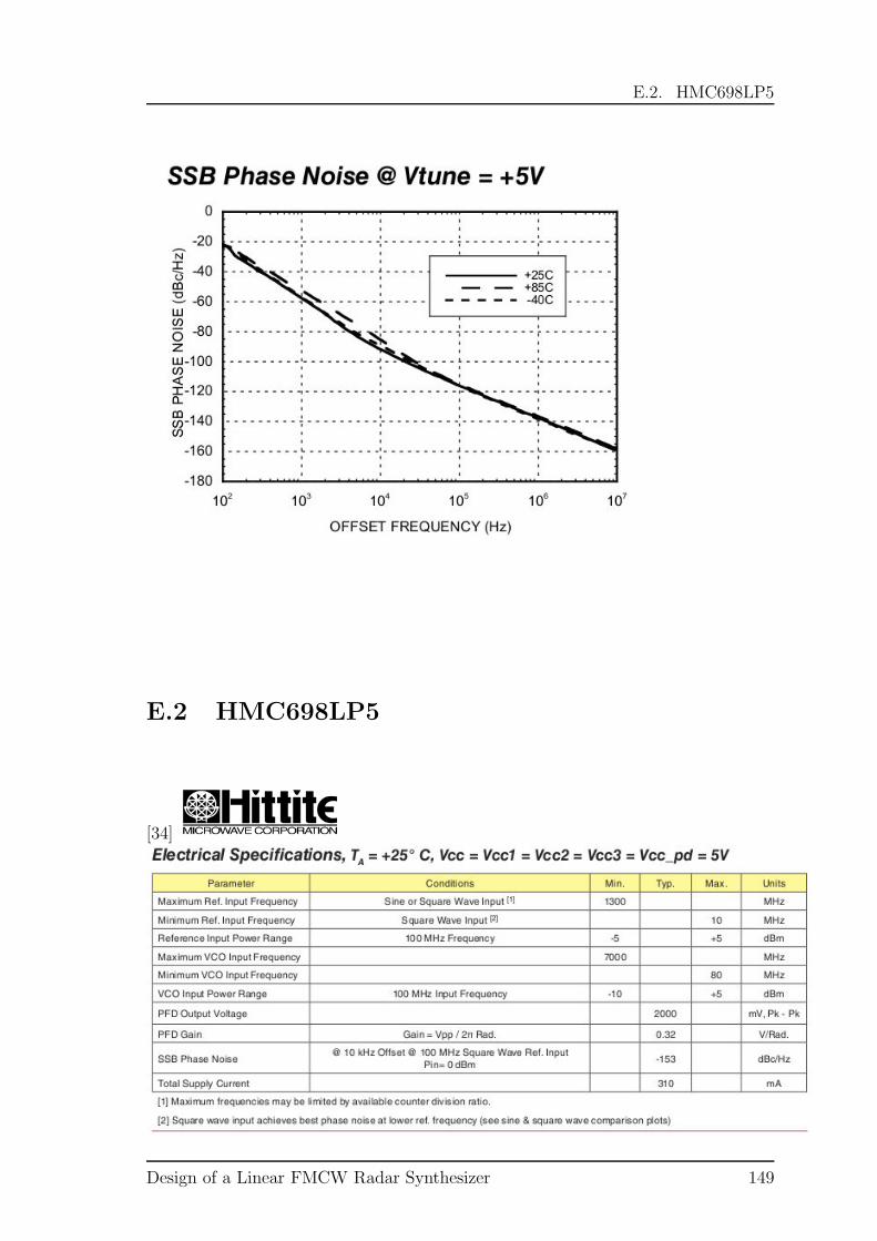
E.2. HMC698LP5
E.2 HMC698LP5
[34]
Design of a Linear FMCW Radar Synthesizer 149

APPENDIX E. DATASHEETS
LD
INV
N/C
Vcc1
Vcc3
N/C
N/C
N/C
N0
N1
N2
N3
N4
N5
FIN
NFIN
GND
N/C
S0
S1
N/C
N/C
N/C
Vcc2
N/C
N/C
NU
ND
N/C
REF
NREF
N/C
Vcc_pd
150 Ruben Undheim
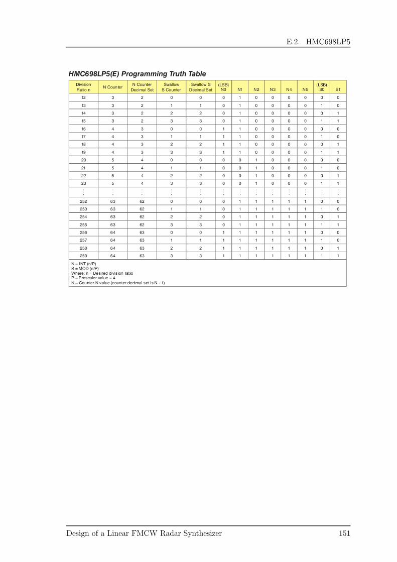
E.2. HMC698LP5
Design of a Linear FMCW Radar Synthesizer 151

APPENDIX E. DATASHEETS
E.3 AD9858
[29]
152 Ruben Undheim

E.3. AD9858
Design of a Linear FMCW Radar Synthesizer 153

APPENDIX E. DATASHEETS
154 Ruben Undheim

E.4. VFTX210
E.4 VFTX210
[28]
Design of a Linear FMCW Radar Synthesizer 155
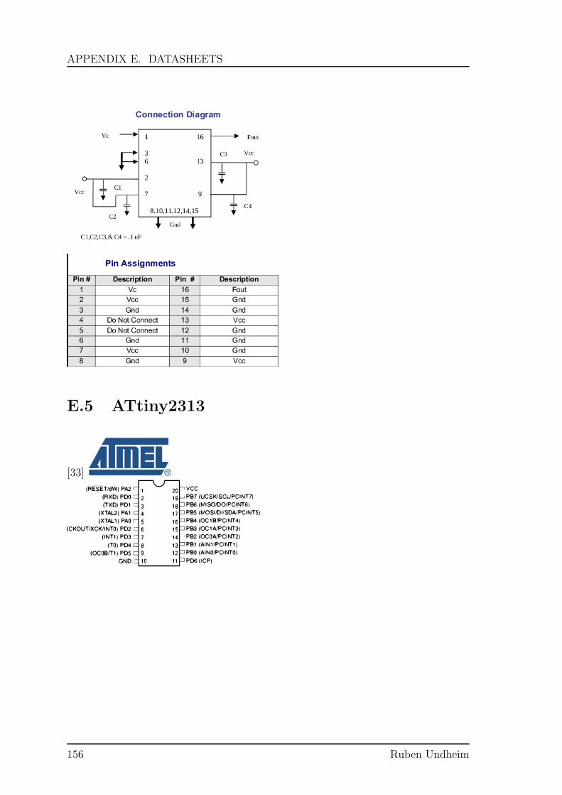
APPENDIX E. DATASHEETS
E.5 ATtiny2313
[33]
156 Ruben Undheim