Design of a 40 GHz low noise amplifier using multigate ...
11
Design of a 40 GHz low noise amplifier using multigate technique for cascode devices Rana Azhar Shaheen 1 • Timo Rahkonen 1 • Aarno Pa ¨ rssinen 1 Received: 3 July 2020 / Revised: 3 July 2020 / Accepted: 24 September 2020 / Published online: 15 October 2020 Ó The Author(s) 2020 Abstract Increased parasitic components in silicon-based nanometer (nm) scale active devices have various performance trade-offs between optimizing the key parameters, for example, maximum frequency of oscillation (f max , gate resistance and capacitance, etc. A common-source cascode device is commonly used in amplifier designs at RF/millimeter-wave (mmWave) frequencies. In addition to intrinsic parasitic components, extrinsic components due to wiring and layout effects, are also critical for performance and accurate modelling of the devices. In this work, a comparison of two different layout techniques for cascode devices is presented to optimize the extrinsic parasitic elements, such as gate resistance. A multi-gate or multi-port layout technique is proposed for optimizing the gate resistance (r g ). Extracted values from measurement results show reduction of 10% in r g of multi-gate layout technique compared to a conventional gate-above- device layout for cascode devices. However, conventional layout exhibits smaller gate-to-source and gate-to-drain capacitances which leads to better performance in terms of speed, i.e. f max . An LNA is designed at 40 GHz frequency using proposed multi-gate cascode device. LNA achieves a measured peak gain of 10.2 dB and noise figure of 4.2 dB at 40 GHz. All the structures are designed and fabricated using 45 nm CMOS silicon on insulator (SOI) technology. Keywords mm-wave RF LNA Receiver 5G Multi-gate Communication systems CMOS SOI 1 Introduction Existing wireless communication technology can not cope up with the increasing demands of data rates from wireless networks due to the increased number of multimedia applications and devices. More complex and higher-order modulation techniques, for example, quadrature amplitude modulation (QAM), are inevitabely required to meet the next generation network capacity demands. This also requires higher values of signal-to-noise ratio (SNR) of the radio frequency front end (RF FE) modules. Due to the non-availability of enough bandwidth (BW) of existing mobile communication technologies, utilization of unused mmWave frequency bands for fifth generation mobile communication (5G) is needed. Third generation partner- ship project (3GPP) has standardized the first frequency bands for 5G new radio (5GNR) from 24 to 29 GHz and 39 GHz. Different 5GNR frequency bands with available BW are listed in Table 1. Moving to mmWave communication also leads to lots of challenges in terms of path loss, scalability, packaging and its associated parasitic effects. Due to that phased arrays are used to increase the antenna aperture in order to com- pensate free space path loss at mmWave frequencies [2]. Miniaturization of bigger antenna systems is realized using silicon based technologies (CMOS and BiCMOS) which offer integrated solutions for faster and scalable mmWave systems for phased arrays [3]. Applications of silicon based technologies are classified by the performance of their active devices and passive structures. For example, nanoscale bulk CMOS technologies offer ultra fast tran- sistors which are useful for logic or digital circuitry. However, they have low ohmic substrate which results in & Rana Azhar Shaheen rana.shaheen@oulu.fi Timo Rahkonen Timo.Rahkonen@oulu.fi Aarno Pa ¨rssinen Aarno.Parssinen@oulu.fi 1 University of Oulu, Oulu, Finland 123 Analog Integrated Circuits and Signal Processing (2020) 105:347–357 https://doi.org/10.1007/s10470-020-01722-w
Transcript of Design of a 40 GHz low noise amplifier using multigate ...

Design of a 40 GHz low noise amplifier using multigate techniquefor cascode devices
Rana Azhar Shaheen1 • Timo Rahkonen1 • Aarno Parssinen1
Received: 3 July 2020 / Revised: 3 July 2020 / Accepted: 24 September 2020 / Published online: 15 October 2020� The Author(s) 2020
AbstractIncreased parasitic components in silicon-based nanometer (nm) scale active devices have various performance trade-offs
between optimizing the key parameters, for example, maximum frequency of oscillation (fmax, gate resistance and
capacitance, etc. A common-source cascode device is commonly used in amplifier designs at RF/millimeter-wave
(mmWave) frequencies. In addition to intrinsic parasitic components, extrinsic components due to wiring and layout
effects, are also critical for performance and accurate modelling of the devices. In this work, a comparison of two different
layout techniques for cascode devices is presented to optimize the extrinsic parasitic elements, such as gate resistance. A
multi-gate or multi-port layout technique is proposed for optimizing the gate resistance (rg). Extracted values from
measurement results show reduction of 10% in rg of multi-gate layout technique compared to a conventional gate-above-
device layout for cascode devices. However, conventional layout exhibits smaller gate-to-source and gate-to-drain
capacitances which leads to better performance in terms of speed, i.e. fmax. An LNA is designed at 40 GHz frequency using
proposed multi-gate cascode device. LNA achieves a measured peak gain of 10.2 dB and noise figure of 4.2 dB at 40 GHz.
All the structures are designed and fabricated using 45 nm CMOS silicon on insulator (SOI) technology.
Keywords mm-wave � RF � LNA � Receiver � 5G � Multi-gate � Communication systems � CMOS � SOI
1 Introduction
Existing wireless communication technology can not cope
up with the increasing demands of data rates from wireless
networks due to the increased number of multimedia
applications and devices. More complex and higher-order
modulation techniques, for example, quadrature amplitude
modulation (QAM), are inevitabely required to meet the
next generation network capacity demands. This also
requires higher values of signal-to-noise ratio (SNR) of the
radio frequency front end (RF FE) modules. Due to the
non-availability of enough bandwidth (BW) of existing
mobile communication technologies, utilization of unused
mmWave frequency bands for fifth generation mobile
communication (5G) is needed. Third generation partner-
ship project (3GPP) has standardized the first frequency
bands for 5G new radio (5GNR) from 24 to 29 GHz and
39 GHz. Different 5GNR frequency bands with available
BW are listed in Table 1.
Moving to mmWave communication also leads to lots of
challenges in terms of path loss, scalability, packaging and
its associated parasitic effects. Due to that phased arrays
are used to increase the antenna aperture in order to com-
pensate free space path loss at mmWave frequencies [2].
Miniaturization of bigger antenna systems is realized using
silicon based technologies (CMOS and BiCMOS) which
offer integrated solutions for faster and scalable mmWave
systems for phased arrays [3]. Applications of silicon based
technologies are classified by the performance of their
active devices and passive structures. For example,
nanoscale bulk CMOS technologies offer ultra fast tran-
sistors which are useful for logic or digital circuitry.
However, they have low ohmic substrate which results in
& Rana Azhar Shaheen
Timo Rahkonen
Aarno Parssinen
1 University of Oulu, Oulu, Finland
123
Analog Integrated Circuits and Signal Processing (2020) 105:347–357https://doi.org/10.1007/s10470-020-01722-w(0123456789().,-volV)(0123456789().,-volV)
more losses in passive structures. Contrarily, in addition to
ultra fast transistors, CMOS silicon-on-insulator (SOI)
technology also provides the opportunity to use high
resistive substrate to integrate high performing passive
structures. Moreover, SOI technology reduces substrate
related cross-talk and improves isolation in metal oxide
semiconductor (MOS) based switches. Therefore, CMOS
SOI technology can be considered as a good candidate for
future mmWave integrated systems consisting of RF front
ends as well as digital baseband circuitry on the same chip.
Gate length of a transistor is considered as the major
driving factor towards technology scaling. High frequency
performance of a transistor is determined by the gate length
and its associated parasitic components, i.e. capacitance
and resistance. These parasitic components and their values
highly depend on the layout style. For example, instead of
single side connection, gate resistance (rg) of a multi-finger
device can be reduced significantly with the dual side
connections of poly silicon gate finger to metal 1 (M1) [4].
Advanced silicon technologies offer scalable intrinsic
models for transistors including the realistic parasitic
components up to few metal layers (e.g. M3). However,
signals at mmWave frequency are routed preferably on the
higher metal layers due to their reduced metal resistance
which necessitates the extension of device terminals from
lower to higher metal layers. Modelling of these inter-
connects are part of the extrinsic model of the device and it
relies on the layout techniques adopted by the designer.
These parasitic effects (intrinsic and extrinsic) are present
in the definition of the maximum oscillation frequency of
the device, i.e. fmax, and given as,
fmax ¼1
4p
ffiffiffiffiffiffiffiffiffiffiffiffiffiffiffiffiffiffiffiffiffiffiffiffiffiffiffiffiffiffiffiffiffiffi
gmrgCgdðCgs þ CgdÞ
r
; ð1Þ
where gm is the transconductance of the device and
depends on the current density of the technology, Cgs and
Cgd are the parasitic capacitance at gate terminal. Cascode
devices are largely used in amplifier designs due to their
benefits of better gain and improved stability conditions.
Aforementioned modelling approach of a single device can
also be applicable to characterize the CS stage with cas-
code device and it can be treated as a three terminal device
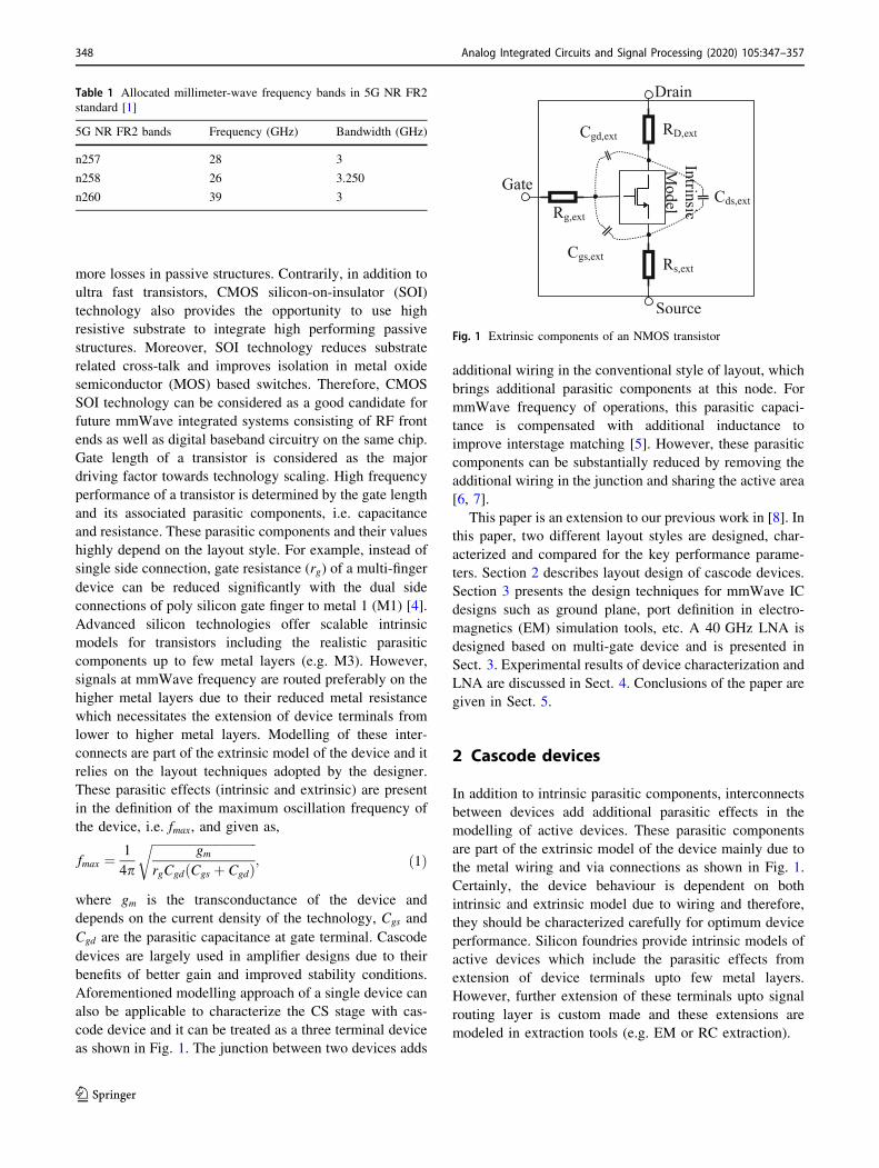
as shown in Fig. 1. The junction between two devices adds
additional wiring in the conventional style of layout, which
brings additional parasitic components at this node. For
mmWave frequency of operations, this parasitic capaci-
tance is compensated with additional inductance to
improve interstage matching [5]. However, these parasitic
components can be substantially reduced by removing the
additional wiring in the junction and sharing the active area
[6, 7].
This paper is an extension to our previous work in [8]. In
this paper, two different layout styles are designed, char-
acterized and compared for the key performance parame-
ters. Section 2 describes layout design of cascode devices.
Section 3 presents the design techniques for mmWave IC
designs such as ground plane, port definition in electro-
magnetics (EM) simulation tools, etc. A 40 GHz LNA is
designed based on multi-gate device and is presented in
Sect. 3. Experimental results of device characterization and
LNA are discussed in Sect. 4. Conclusions of the paper are
given in Sect. 5.
2 Cascode devices
In addition to intrinsic parasitic components, interconnects
between devices add additional parasitic effects in the
modelling of active devices. These parasitic components
are part of the extrinsic model of the device mainly due to
the metal wiring and via connections as shown in Fig. 1.
Certainly, the device behaviour is dependent on both
intrinsic and extrinsic model due to wiring and therefore,
they should be characterized carefully for optimum device
performance. Silicon foundries provide intrinsic models of
active devices which include the parasitic effects from
extension of device terminals upto few metal layers.
However, further extension of these terminals upto signal
routing layer is custom made and these extensions are
modeled in extraction tools (e.g. EM or RC extraction).
Fig. 1 Extrinsic components of an NMOS transistor
Table 1 Allocated millimeter-wave frequency bands in 5G NR FR2
standard [1]
5G NR FR2 bands Frequency (GHz) Bandwidth (GHz)
n257 28 3
n258 26 3.250
n260 39 3
348 Analog Integrated Circuits and Signal Processing (2020) 105:347–357
123

2.1 Optimization of rg or fmax
Amongst all the other parameters in Eq. 1, gate to drain
capacitance (Cgd) and gate resistance (rg) are the most
critical in terms of optimum device performance. Cascode
devices improve the stability of the amplifier due to
increased isolation between input and output (smaller val-
ues of Cgd). When designing an LNA, the main target
towards optimum device performance is to optimize the
active device for maximum fmax or lowest rg. Total gate
resistance is composed of different contributors from
intrinsic and extrinsic vias, external wiring, etc. and is
given in [9] as
Rg;tot ¼ Rh þ Rv þ rvia;int þ rvia;ext þ rwire; ð2Þ
where Rh and Rv are horizontal and vertical resistance of a
single gate finger, respectively. rvia is the resistance of poly
to metal contact and rwire is the resistance of interconnect
for external wiring. Rh and Rv are included in the intrinsic
model of the device. While rwire and part of the rvia depend
on the external routing. All of these contributors can be
reduced to an optimum value by using efficient layout
techniques. For example, increasing number of fingers and
gate contacts for each finger helps to significantly reduce in
values of rh, rv, and rvia. Intrinsic interconnect rvia;int is the
resistance from poly to m1 and can be reduced by con-
necting each gate poly at both ends, as shown in Fig. 2.
rvia;ext is the extrinsic resistance of via from metal M1 to
thick metal layers, e.g. M7.
In addition to various benefits, cascode devices have
also limitations of the voltage swing for low voltage power
supply designs, and additional wiring capacitance at
intermediate node and at the output node. In mm-Wave
frequency designs, inter-stage matching is used to resonate
out the wiring capacitance between the transistors [7].
However, these junction-based capacitance can be reduced
significantly by removing the metal wiring in the junction
and sharing the active area between the two devices in
cascode. Multigate technique for stacked devices proposed
in [6], is one possible way in reducing inter-stage wiring
parasitics. In this work, design and comparison of two
layout techniques for cascode devices, i.e. conventional
style and multi-gate style, is presented. Proposed multi-
gate style layout helps to reduce inter-stage wiring as dis-
cussed in [6], and allows a larger number of metal M1-to-
M5 vias implemented for the same area of device com-
pared to conventional layout. This increased number of
metal M1–M5 vias help to further reduce rvia;ext as in Eq. 2.
These devices are designed and fabricated using 45 nm
CMOS SOI technology. Transistor size 20 lm for each
layout style having 20 gate fingers is selected for
comparison.
2.2 Conventional style layout
Figure 2 shows a conventional gate-above-device layout
style of a cascode device [4]. Two transistors are placed in
a vertical orientation on top of each other. To reduce Rg;int
of transistors, gate fingers are double connected from two
sides using a ring of metal M1. Input signal from a ground-
signal-ground (GSG) pad is routed at metal M7 and
brought to M5 near the gate of common-source device M1,
which is routed over the transistor and connected gate ring
at metal M1 from two sides in the horizontal direction, as
shown in Fig. 2. In order to achieve enough current han-
dling capability of metal wires, source and drain connec-
tions of each finger is brought up to metal M2 to M4 and
connected together with a wider stack of metal layers from
M2–M4. These connections are extended further and con-
nected to thick metal layer M7. This further extension of
drain and source connections helps to reduce the additional
capacitive coupling due to thick metal lines between dif-
ferent nodes, e.g. cgg ¼ cgd þ cgs.
2.3 Multi-gate style layout
Multi-gate layout technique is drawn by sharing the active
area of two transistors to eliminate intermediate metal
contacts of drain and source terminals between the tran-
sistors for cascode devices [6, 7]. A unit cell of a 1um
finger width using multi-gate technique is shown in
Fig. 3(a). Each cell has double connected gate finger at
metal M1. Source and drain connections are extended
further from the device using stack of metal M2–M4. A
distribution network of such cells is placed in a vertical
orientation such that the gate connection at metal M1 is
shared between two cells. A M1–M5 via is placed in thisFig. 2 Conventional-style schematic and layout of cascode devices
Analog Integrated Circuits and Signal Processing (2020) 105:347–357 349
123

shared area of gate at M1. This increases the number of
vias at gate terminal. Gate signal is routed at metal M5
from top of the structure and tapped to the gate contacts
using these M1–M5 vias. A device schematic and layout
schemes are shown in Fig. 3(b), which is composed of 20
unit cells in a tree configuration. Similarly, source con-
nection of the cells are shared between two adjacent cells
and routed from the middle of the cells towards bottom of
the structure not crossing the gate wiring to minimize the
gate-to-source capacitance. Drains of the cells are con-
nected to metal M7 and routed from two sides of the
structures to bottom of the structure. As it can be seen from
Fig. 3(b), there are at least four times the number of M1-to-
M5 vias compared to the structure in Fig. 2 to reduce
rvia;ext. Similarly wiring resistance is halved by routing the
gate signal at metal M5 in two parallel branches, which
helps to reduce the rwire. The layout presented in Fig. 3(b)
is good for optimizing rg;ext. However, due to the increased
wiring at the drain terminals of the structure, cgd is
increased, which limits the fmax of the device. This is
acceptable when fmax is not too close to the actual operation
frequency.
3 mmWave design techniques
3.1 RF ground for inductors and transformers
EM modelling techniques are used in order to accurately
include the behavior of a multi-layer passive device and its
associated RF ground in the overall device performance. A
low impedance ground plane for passive devices is very
important in mmWave integrated circuit designs to provide
seamless path for high frequency return currents. Definition
of an RF ground is essential for ground reference of the
excitation ports. Two possible ground plane definitions are
shown in Fig. 4. Bottom side of the substrate can be used
as RF ground (Fig. 4(a)) that requires solid connections
(through-hole via) from top metal layer through substrate
[10] because external ground connections to chip are only
possible through metal bond pads. However, manufactur-
ing of these vias are expensive and require extra
(a)
(b)
Fig. 3 Multi-gate device schematic and layout a single unit cell and
multi-cell schematic, b layout of single cell and multiple cells
(a)
(b)
Fig. 4 Port difinition, a port reference from the bottom of the
substrate, b port reference from local ground plane
350 Analog Integrated Circuits and Signal Processing (2020) 105:347–357
123
manufacturing processing [11]. Moreover, eddy currents
can be induced in this solid metal plate resulting in sub-
stantial loss in passive devices at mmWave frequencies.
Contrarily, a local ground plane can be used as an RF
ground reference which provides local reference for the
excitation ports as shown in Fig. 4(b). Generally, a ground
plane is composed of thick metal layer from the available
metal stack of the technology due to their lower sheet
resistance. Alternatively, multiple metal layers are stacked
together to realize low impedance metal ground plane.
In bulk CMOS process, low resistive substrate requires
metal ring (guard ring) connected with the metal ground
plane around active and passive devices in order to offer
low ohmic paths for currents induced from substrate cou-
pling to reduce cross talks between neighbouring devices.
In such case, a wall of ground plane around passive devices
consisting of all metal layers is used which offers addi-
tional benefits of isolation between neighbouring devices.
However, in high-resistive substrates, e.g. CMOS SOI,
substrate connections (guard ring) are not necessary around
passive devices and therefore, a metal ground plane at top
metal layer with enough current handling capability is
sufficient as shown in Fig. 4(b).
External transistion of signal and ground connections
from the chip to outside world, i.e. printed circuit board
(PCB), are realized using bond pads made of top metal
layer. These bond pads are then connected to PCB with the
help of bond wires or solder balls. Parasitic inductance
(� 100 s of pH) and resistance associated with bond wires
make them non-feasible for most of the mmWave appli-
cations. Contrarily, solder balls have very low parasitic
inductance (� 10 s of pH) [12] from the connections
when connected in flip chip orientation as shown in
Fig. 5(a). When designing the mmWave circuit blocks
(passive or active), extracted models of these signal and
ground transitions should be included in the simulations.
An RF ground can also be defined outside the chip, i.e.
PCB, considering the IC is connected on the PCB as flipped
chip using solder balls as shown in Fig. 5(b). In such case,
top PCB layer (RF ground) interfacing with IC should be
part of the EM simulations. This type of RF ground has
minimum transition between PCB and IC and represents
more realistic simulation environment towards real
implementation.
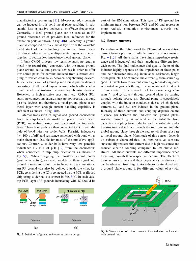
3.2 Return currents
Depending on the definition of the RF ground, an excitation
current from a port finds multiple return paths as shown in
Fig. 6 [13]. All these paths have finite impedance (resis-
tance and inductance) and their lengths are different from
each other. The final inductance and quality factor of the
inductor highly depends on the impedance of these paths
and their characteristics, e.g. inductance, resistance, length
of the path, etc. For example, the current it1 from source vt1(port 1) travels towards output source vt2 (considering port2
is shorted to ground) through the inductor and it takes 4
different return paths to reach back to its source vt1. Cur-
rents ir1 and ir2 travels through ground plane by passing
through voltage source vt2. Ground plane is capacitively
coupled with the inductor conductor, due to which electric
currents (ir3 and ir4) are induced in the ground plane.
Intensity of these currents and coupling depends on the
distance (d) between the inductor and ground plane.
Another current ir5 is induced in the substrate from
capacitive coupling from inductor and the substrate under
the structure and it flows through the substrate and into the
global ground plane through the nearest via from substrate
to metal ground plane. Magnitude of this current depends
on substrate characteristics, i.e. high-resistive substrate
substantially reduces this current due to high resistance and
reduced electric coupling compared to low-ohmic sub-
strates. All these currents see different impedance when
travelling through their respective medium. The effects of
these return currents and their dependency on distance d
can be observed from Fig. 7. An inductor is simulated with
a ground plane around it for different values of d (with
(a) (b)
Fig. 5 Definition of ground reference in passive design
Fig. 6 Visualization of return currents of an inductor implemented
with ground ring
Analog Integrated Circuits and Signal Processing (2020) 105:347–357 351
123
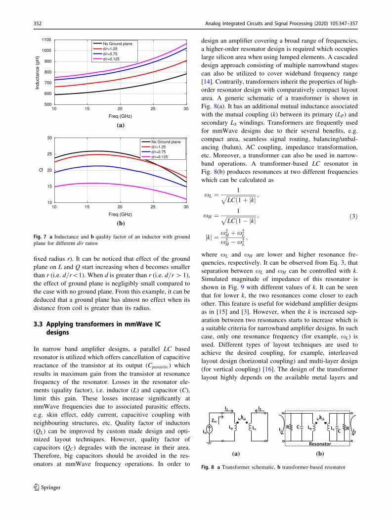
fixed radius r). It can be noticed that effect of the ground
plane on L and Q start increasing when d becomes smaller
than r (i.e. d=r\1). When d is greater than r (i.e. d=r[ 1),
the effect of ground plane is negligibly small compared to
the case with no ground plane. From this example, it can be
deduced that a ground plane has almost no effect when its
distance from coil is greater than its radius.
3.3 Applying transformers in mmWave ICdesigns
In narrow band amplifier designs, a parallel LC based
resonator is utilized which offers cancellation of capacitive
reactance of the transistor at its output (Cparasitic) which
results in maximum gain from the transistor at resonance
frequency of the resonator. Losses in the resonator ele-
ments (quality factor), i.e. inductor (L) and capacitor (C),
limit this gain. These losses increase significantly at
mmWave frequencies due to associated parasitic effects,
e.g. skin effect, eddy current, capacitive coupling with
neighbouring structures, etc. Quality factor of inductors
(QL) can be improved by custom made design and opti-
mized layout techniques. However, quality factor of
capacitors (QC) degrades with the increase in their area.
Therefore, big capacitors should be avoided in the res-
onators at mmWave frequency operations. In order to
design an amplifier covering a broad range of frequencies,
a higher-order resonator design is required which occupies
large silicon area when using lumped elements. A cascaded
design approach consisting of multiple narrowband stages
can also be utilized to cover wideband frequency range
[14]. Contrarily, transformers inherit the properties of high-
order resonator design with comparatively compact layout
area. A generic schematic of a transformer is shown in
Fig. 8(a). It has an additional mutual inductance associated
with the mutual coupling (k) between its primary (LP) and
secondary LS windings. Transformers are frequently used
for mmWave designs due to their several benefits, e.g.
compact area, seamless signal routing, balancing/unbal-
ancing (balun), AC coupling, impedance transformation,
etc. Moreover, a transformer can also be used in narrow-
band operations. A transformer-based LC resonator in
Fig. 8(b) produces resonances at two different frequencies
which can be calculated as
xL ¼ 1ffiffiffiffiffiffiffiffiffiffiffiffiffiffiffiffiffiffiffiffiffi
LCð1þ jkjp ;
xH ¼ 1ffiffiffiffiffiffiffiffiffiffiffiffiffiffiffiffiffiffiffiffiffi
LCð1� jkjp ;
jkj ¼ x2H þ x2
L
x2H � x2
L
;
ð3Þ
where xL and xH are lower and higher resonance fre-
quencies, respectively. It can be observed from Eq. 3, that
separation between xL and xH can be controlled with k.
Simulated magnitude of impedance of this resonator is
shown in Fig. 9 with different values of k. It can be seen
that for lower k, the two resonances come closer to each
other. This feature is useful for wideband amplifier designs
as in [15] and [3]. However, when the k is increased sep-
aration between two resonances starts to increase which is
a suitable criteria for narrowband amplifier designs. In such
case, only one resonance frequency (for example, xL) is
used. Different types of layout techniques are used to
achieve the desired coupling, for example, interleaved
layout design (horizontal coupling) and multi-layer design
(for vertical coupling) [16]. The design of the transformer
layout highly depends on the available metal layers and
(a)
(b)
Fig. 7 a Inductance and b quality factor of an inductor with ground
plane for different d/r ratios
(a) (b)
Fig. 8 a Transformer schematic, b transformer-based resonator
352 Analog Integrated Circuits and Signal Processing (2020) 105:347–357
123

their respective properties (i.e. thickness, sheet resistance,
etc.).
4 LNA design
In order to optimize the input noise of the LNA towards
minimum noise figure (NFmin), two main factors are con-
sidered, i.e. optimum noise match and minimizing the
intrinsic and extrinsic gate resistance. Intrinsic gate resis-
tance is optimized by optimizing the number of gate fingers
and by increasing the poly to M1 contacts of the gate fin-
gers. Extrinsic gate resistance is reduced by optimizing the
transition of gate from M1 to higher metal layers increasing
the number of M1 to M5 vias. Proposed multi-gate tech-
nique of cascode device layout as discussed in Sect. 2 helps
to reduce the wiring resistance at the gate terminal and can
be useful for low noise amplifier designs.
An inductively degenerated common source cascode
LNA is designed using multigate layout technique. The
proposed LNA is fabricated using 45 nm CMOS SOI
technology at center frequency of 40 GHz. Schematics of
the designed LNA is shown in Fig. 10. A unit cell of
cascode connected devices is designed first and then a
bigger device is designed based on these unit cells. In
addition to the fast active devices, high quality factor
passive structures play a key role in mmWave frequency
designs. CMOS SOI technology provides not only benefits
of reduced parasitics, higher fmax for active devices, but
also offers high resistive substrate that allows the design of
low loss passive structures. Presumably, CMOS SOI
technology is being considered as an attractive choice for
future mmWave integrated system designs. Moreover,
availability of two thick metal layers in metal stack offers
additional design freedom towards low-ohmic passive
structures, such as inductors, transmission lines, trans-
formers and various interconnects.
In this design, a narrowband input matching approach is
used. Source inductance is realized by coplanar waveguide
(CPW) transmission line, and a custom inductor is used for
gate inductance. Layout of the gate inductor is similar to
Fig. 6. CPW transmission line (TL) is designed using thick
copper layer of M8. Since the required degeneration
inductance is small, use of CPW TL provides benefits of
lower inductance with compact area integration.
A one turn transformer with high k is used to resonate
the capacitance at the drain of the cascode devices. Vertical
coupling between the primary and secondary coils is
achieved by stacking the M6 and M7 as shown in Fig. 11.
Transformer was designed for maximum coupling
(k� 0:84) that produces two resonances separated far from
each other and only the lower resonance at 40 GHz is used
(also shown in Fig. 9, black trace). Ground reference port
definition strategy discussed in Sect. 3, is used for EM
simulations of the passive structures. Transformer is also
performing balun function, providing differential signal at
the output of the first stage. An output differential buffer
with the similar transformer load is used as the second
stage of the LNA.
5 Measurement results
In order to make a comparison of multi-gate cascode
device with conventional style layout, two separate struc-
tures are fabricated using 45 nm CMOS SOI technology.
The first device is using conventional style layout, and the
second device utilizes multi-gate technique. Schematic of
the measurement configurations and die micrographs of
Fig. 9 Impedance of a transformer with varying coupling
Fig. 10 Schematic of the LNA Fig. 11 3D layout view of a 1 turn transformer with lateral coupling
Analog Integrated Circuits and Signal Processing (2020) 105:347–357 353
123

both structures are shown in Fig. 12. S-parameter mea-
surements are performed from 30 to 50 GHz frequency
range, using Keysight 67 GHz PNA. GSG pads and probes
are used to measure the s-parameters at the input and
output. Two port calibration is performed up to the probe
tip using external through-reflect-load (TRL) standards on
a separate calibration substrate. DC biasing for gate and
drain of the structures are provided using bias-T from
external sources. However, biasing of cascoded transistors
are provided from on-chip power supply (VDD = 1 V)
with enough decoupling capacitors. Measurement results
include the input and output pads and extended transmis-
sion lines up to the device terminals.
Gate resistance of the structures are extracted from the
measured s-parameters (at fixed bias voltage of 580 mV)
using real part of h11 as also used in [9] and plotted in
Fig. 13.
rg ¼ Reðh11Þ ð4Þ
Gate capacitance (Cgs and Cgd) and transconductance (gm)
are extracted using following equations [17],
Cgs ¼Imðy11 þ y12Þ
x
Cgd ¼ � Imðy12Þx
gm ¼ Reðy21Þ
ð5Þ
Extracted gate resistance of the multi-gate layout technique
is 10% lower than the conventional layout style. However,
due to the increased wiring of the multi-gate technique,
gate to source (Cgs) and gate-to-drain capacitance (Cgd) are
4% and 40% higher than in the conventional layout, as
shown in Fig. 14. There is roughly no change in the
transconductance of both structures, as shown in Fig. 15.
Due to the increase in Cgg, fmax of multi-gate device is 20%
lower than the conventional layout as shown in Fig. 16.
However, this is still sufficient for targeted frequency
bands. Since the detailed modelling for multigate devices
differs from the conventional transistors, measurements
instead of simulations are used for comparison between
two structures. Table 2 shows comparison results of
extracted parameters at 40 GHz for the two structures
(Fig. 12).
Fig. 12 Die micrographs of cascode structures and respective
schematics
Fig. 13 Extracted Rg of two structures (VDD = 1 V,
Vbias ¼ 580 mV)
Fig. 14 Extracted capacitances, Cgs and Cgd of two structures,
(VDD = 1 V, Vbias ¼ 580 mV)
Fig. 15 Extracted gm of two structures, (VDD = 1 V,
Vbias ¼ 580 mV)
354 Analog Integrated Circuits and Signal Processing (2020) 105:347–357
123
A single-ended input, differential output LNA is fabri-
cated using GlobalFoundries 45 nm CMOS SOI technol-
ogy. Die micrograph of LNA is shown in Fig. 17, core area
including input and output pads is 1061� 0:349mm2.
Although, it is better to compare the layout effects of two
styles on the noise performance of an LNA. However, this
was not possible due to the limited available resources for
chip fabrication. GSG probes are used to perform on wafer
measurements. LNA is measured from a single-ended input
to a single-ended output because of the non availability of
single-to-differential probe calibration. S-parameters of the
LNA are measured using Keysight 67 GHz PNA. Noise
figure measurements are performed using 50 GHz noise
source, 50 GHz spectrum analyzer and pre-amplifier pro-
vided by Keysight technologies. Calibration of the noise
figure measurement setup is performed using on-chip
through standard. Biasing of the active blocks is imple-
mented using local current mirrors which take 100 lmcurrent from off-chip external source using bondwire
connections. Biasing voltage is controlled using on-chip
integrated shift register logic. Supply voltage is also routed
from external supply using bondwire connections with
sufficient supply de-coupling capacitance placed on- and
off-chip. Measured and simulated s-parameters and noise
figure results for dual-gate LNA are shown in Fig. 18(a, b),
respectively. Measured S21 gain is 10.2 dB at 40 GHz.
Measured input (S11) and output (S22) reflection coeffi-
cient are below - 10 dB at 40 GHz. Noise figure is 4.3 dB
at 40 GHz. Table 3 shows a brief performance comparison
of the LNA with existing state-of-the-art (SOA) designs at
40 GHz. Measured (and simulated) gain of the LNA is
around 3 dB lower because it was measured (and simu-
lated) from single-ended output only. It shows that LNA is
having much lower power consumption with the LNA’s of
similar performance.
Fig. 16 Extracted fmax versus Vbias of two structures
Fig. 17 Micrograph of the LNA
(a)
(b)
Fig. 18 Measured s-parameters of LNA
Table 2 Comparison table of extracted parameter values at 40 GHz
(VDD = 1 V, Vbias ¼ 580 mV)
Parameters Conventional Multigate
Rg (X) 14.3 12.9
Cgs (fF) 60 62
Cgd (fF) 2.77 4.33
gm (mS) 22.5 22.5
fmax (GHz) 243 215
Analog Integrated Circuits and Signal Processing (2020) 105:347–357 355
123

6 Conclusion
This work introduces layout optimization techniques of
cascode connected transistors and a design of an LNA for
mmWave applications. A multi-gate layout technique is
compared to a conventional layout style. Optimization of
intrinsic and extrinsic parasitic components for both cas-
code devices is discussed. Design techniques of silicon
based passive structures for mmWave applications are
discussed and optimization of ground connection pre-
sented. An overview was given for setting up the ground
reference for port definition in EM simulation tools. Design
of a 40 GHz LNA using multi-gate cascode device is also
presented including key results from fabricated sample. A
multi-gate layout reduces gate resistance while conven-
tional layout reduces wiring capacitance. It is compared
against cascode LNA’s. The device is designed and fabri-
cated using 45 nm CMOS SOI technology. Measurement
results show a reduction of 10% in gate resistance of multi-
gate layout technique compared to the conventional double
contacted gate approach. However, gate-to-source and
gate-to-drain capacitances are degraded by 4% and 36%,
respectively, which limits the maximum speed of the input
stage. Therefore, this comparison concludes that there is a
trade-off in optimization between rg and fmax of the cascode
devices in layout designs. Measured results of LNA
achieve a peak gain of 10.2 dB and noise figure of 4.2 dB
at 40 GHz.
Acknowledgements The authors would like to thank Nokia Corpo-
ration for financial support and Global Foundries for support in pro-
cess technology. Lab assistance from Matti Polojarvi is highly
acknowledged. This research has been also in part financially sup-
ported by Academy of Finland 6Genesis Flagship (Grant 318927).
Open Access This article is licensed under a Creative Commons
Attribution 4.0 International License, which permits use, sharing,
adaptation, distribution and reproduction in any medium or format, as
long as you give appropriate credit to the original author(s) and the
source, provide a link to the Creative Commons licence, and indicate
if changes were made. The images or other third party material in this
article are included in the article’s Creative Commons licence, unless
indicated otherwise in a credit line to the material. If material is not
included in the article’s Creative Commons licence and your intended
use is not permitted by statutory regulation or exceeds the permitted
use, you will need to obtain permission directly from the copyright
holder. To view a copy of this licence, visit http://creativecommons.
org/licenses/by/4.0/.
Funding Open access funding provided by University of Oulu
including Oulu University Hospital.
References
1. 3GPP, User equipment (UE) radio transmission and reception
(release 15), 3rd Generation Partnership Project (3GPP), Tech-
nical Specification (TS), December 2018.
2. MacCartney, G. R., Zhang, J., Nie, S., & Rappaport, T. S. (2013).
Path loss models for 5g millimeter wave propagation channels in
urban microcells. In 2013 IEEE global communications confer-ence (GLOBECOM) (pp. 3948–3953).
3. Mondal, S., Singh, R., Hussein, A. I., & Paramesh, J. (2018). A
25–30 GHz fully-connected hybrid beamforming receiver for
MIMO communication. IEEE Journal of Solid-State Circuits,53(5), 1275–1287.
4. Sharma, J., & Krishnaswamy, H. (2013). 216- and 316-GHz
45-nm SOI CMOS signal sources based on a maximum-gain ring
oscillator topology. IEEE Transactions on Microwave Theoryand Techniques, 61(1), 492–504.
5. Qin, P., & Xue, Q. (2017). Compact wideband LNA with gain
and input matching bandwidth extensions by transformer. IEEEMicrowave and Wireless Components Letters, 27(7), 657–659.
6. Jayamon, J. A., Buckwalter, J. F., & Asbeck, P. M. (2016).
Multigate-cell stacked FET design for millimeter-wave CMOS
power amplifiers. IEEE Journal of Solid-State Circuits, 51(9),2027–2039.
7. Datta, K., & Hashemi, H. (2017). High-breakdown, high- fmax
multiport stacked-transistor topologies for the W -band power
amplifiers. IEEE Journal of Solid-State Circuits, 52(5),1305–1319.
8. Shaheen, R. A., Rahkonen, T., Akbar, R., Aikio, J. P., Sethi, A.,
& Prssinen, A. (2019). Layout optimization techniques for rg and,fmax of cascode devices for mm wave applications. In 2019 IEEEnordic circuits and systems conference (NORCAS): NORCHIPand international symposium of system-on-chip (SoC) (pp. 1–4).
9. Wachnik, R. A., Lee, S., Pan, L. H., Lu, N., Li, H., Bingert, R.,
Randall, M., Springer, S., & Putnam, C. (2013). Gate stack
resistance and limits to CMOS logic performance. In Proceedingsof the IEEE 2013 custom integrated circuits conference (pp. 1–4).
10. Pham, N. P., Sarro, P. M., Ng, K. T., & Burghartz, J. N. (2001).
A micromachining post-process module with pattern transfer in
deep cavities for rf silicon technology. In Technical digest.MEMS 2001. 14th IEEE international conference on microelectro mechanical systems (Cat. No.01CH37090) (pp. 345–348).
11. Phuong Pham, ga, Sarro, P. M., Ng, K. T., & Burghartz, J. N.
(2001). IC-compatible two-level bulk micromachining process
Table 3 Perfomrance
comparison of LNA with
existing SOA LNAs
Technology This work [18] [19] [20] [21]
45 nm SOI 130 nm CMOS 90 nm CMOS 65 nm CMOS 90 nm SOI
Freq (GHz) 40 38 37 42 26–42
Max. gain (dB) 10.2 12.6 13.8 14.3 11.9
NF (dB) 4.2 4 3.8 6 4.2
Pdiss (mW) 13 24 18 43.2 40.8
P1dB (dBm) - 11 N/A N/A N/A N/A
Chip area (mm2) 0.31 0.252 0.48 0.286 0.18
356 Analog Integrated Circuits and Signal Processing (2020) 105:347–357
123
module for RF silicon technology. IEEE Transactions on Elec-tron Devices, 48(8), 1756–1764.
12. Kodak, U., & Rebeiz, G. M. (2017). Bi-directional flip-chip 28
GHz phased-array core-chip in 45 nm CMOS SOI for high-effi-
ciency high-linearity 5g systems. In 2017 IEEE radio frequencyintegrated circuits symposium (RFIC) (pp. 61–64).
13. Kraemer, M., Dragomirescu, D., & Plana, R. (2010). Accurate
electromagnetic simulation and measurement of millimeter-wave
inductors in bulk CMOS technology. In 2010 topical meeting onsilicon monolithic integrated circuits in RF systems (SiRF) (pp.61–64).
14. Yu, Y., Liu, H., Wu, Y., & Kang, K. (2017). A 54.4–90 GHz low-
noise amplifier in 65-nm CMOS. IEEE Journal of Solid-StateCircuits, 52(11), 2892–2904.
15. Vigilante, M., & Reynaert, P. (2016). 20.10 a 68.1-to-96.4 GHz
variable-gain low-noise amplifier in 28 nm CMOS. In 2016 IEEEinternational solid-state circuits conference (ISSCC) (pp.
360–362).
16. Rimmelspacher, J., Breun, S., Werthof, A., Geiselbrechtinger, A.,
Weigel, R., & Issakov, V. (2018). Experimental comparison of
integrated transformers in a 28 nm bulk CMOS technology. In
2018 48th European microwave conference (EuMC) (pp.
1097–1100).
17. Saijets, J. (2007). Mosfet RF characterization using bulk and SOICMOS technologies. Dissertation.
18. Huang, B., Lin, K., & Wang, H. (2009). Millimeter-wave low
power and miniature CMOS multicascode low-noise amplifiers
with noise reduction topology. IEEE Transactions on MicrowaveTheory and Techniques, 57(12), 3049–3059.
19. Yeh, H., Chiong, C., Aloui, S., & Wang, H. (2012). Analysis and
design of millimeter-wave low-voltage CMOS cascode LNA with
magnetic coupled technique. IEEE Transactions on MicrowaveTheory and Techniques, 60(12), 4066–4079.
20. Varonen, M., Karkkainen, M., Kantanen, M., & Halonen, K. A. I.
(2008). Millimeter-wave integrated circuits in 65-nm CMOS.
IEEE Journal of Solid-State Circuits, 43(9), 1991–2002.21. Ellinger, F. (2004). 26–42 GHz SOI CMOS low noise amplifier.
IEEE Journal of Solid-State Circuits, 39(3), 522–528.
Publisher’s Note Springer Nature remains neutral with regard to
jurisdictional claims in published maps and institutional affiliations.
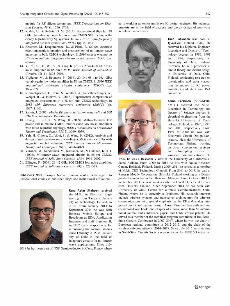
Rana Azhar Shaheen received
the M.Sc. in Electrical Engi-
neering from Tampere Univer-
sity of Technology, Finland, in
2012. From January 2013 to
September 2014 he was with
Renesas Mobile Europe and
Broadcom as EDA Application
Engineer and staff Engineer II,
in RFIC teams, respectively. He
is pursuing his doctoral studies
since February 2015 in Univer-
sity of Oulu in the field of
integrated circuits for millimeter
wave applications. Since July
2019 he has been part of NXP Semiconductor in Caen, France where
he is working as senior mmWave IC design engineer. His technical
interests are in the field of analysis and circuit design of mm-wave
Wireless Transceivers.
Timo Rahkonen was born in
Jyvaskyla, Finland, 1962. He
received his Diploma Engineer,
Licentiate and Doctor of Tech-
nology degrees in 1986, 1991
and 1994, respectively, in
University of Oulu, Finland.
Currently he is a professor in
circuit theory and circuit design
in University of Oulu, Oulu,
Finland, conducting research on
linearization and error correc-
tion techniques for RF power
amplifiers and A/D and D/A
converters
Aarno Parssinen (S’95-M’01-
SM’11) received the M.Sc.,
Licentiate in Technology and
Doctor of Science degrees in
electrical engineering from the
Helsinki University of Tech-
nology, Finland, in 1995, 1997,
and 2000, respectively. From
1994 to 2000 he was with
Electronic Circuit Design Lab-
oratory, Helsinki University of
Technology, Finland, working
on direct conversion receivers
and subsampling mixers for
wireless communications. In
1996, he was a Research Visitor at the University of California at
Santa Barbara. From 2000 to 2011 he was with Nokia Research
Center, Helsinki, Finland. During 2009–2011 he served as a member
of Nokia CEO Technology Council. From 2011 to 2013, he was at
Renesas Mobile Corporation, Helsinki, Finland working as a Distin-
guished Researcher and RF Research Manager. From October 2013 to
September 2014 he was an Associate Technical Director at Broad-
com, Helsinki, Finland. Since September 2014 he has been with
University of Oulu, Centre for Wireless Communications, Oulu,
Finland where he is currently a Professor. His research interests
include wireless systems and transceiver architectures for wireless
communications with special emphasis on the RF and analog inte-
grated circuit and system design. Aarno Parssinen has authored and
co-authored one book, one chapter of a book, more than 50 interna-
tional journal and conference papers and holds several patents. He
served as a member of the technical program committee of Int. Solid-
State Circuits Conference in 2007–2017, where he was the chair of
European regional committee in 2012–2013, and the chair of the
wireless sub-committee in 2014–2017. Since July 2015 he is serving
as Solid-State Circuits Society representative for IEEE 5G initiative.
Analog Integrated Circuits and Signal Processing (2020) 105:347–357 357
123