Design Modulo-4 and Galois Field Adder, Subtractor and ... · Design Modulo-4 and Galois Field...
12
IOSR Journal of VLSI and Signal Processing (IOSR-JVSP) Volume 4, Issue 4, Ver. I (Jul-Aug. 2014), PP 41-52 e-ISSN: 2319 – 4200, p-ISSN No. : 2319 – 4197 www.iosrjournals.org www.iosrjournals.org 41 | Page Design Modulo-4 and Galois Field Adder, Subtractor and Multiplier Using Quaternary Logic 1 Miss. Rajashri R. Korde, 2 Asst.Prof. Dinesh Rotake Abstract: Arithmetic circuits play a very necessary role in every general and application specific procedure circuits. Multiple Valued Logic (MVL)provides the key smart factor concerning future density per circuit area compared to ancient two valued binary logic. Quaternary (Four-valued) logic jointly offers the nice factor concerning easy interfacing to binary logic as a results of base four (=22) permits for the use of easy encoding/decoding circuits. The purposeful completeness is proved with a set of basic quaternary cells. The library of cells supported the Supplementary Symmetrical Logic Circuit Structure (SUSLOC) unit of measurement designed, simulated, and accustomed build several quaternary fixed-point arithmetic circuits like adders, multipliers. These SUSLOC circuit cells unit of measurement valid practice SPICE models and additionally the arithmetic architectures unit of measurement valid practice System Verilog models for purposeful correctness. Quaternary (radix-4) twin amount secret writing principles unit of measurement applied to optimize power and performance of adder circuits practice common place cmos gate technologies. Index Terms: Multiple-valued logic , Quaternary logic, Modulo-n addition , subtraction and multiplication, Galois. Addition and multiplication . I. Introduction The outstanding increase inside the density of very large Scale Integrated (VLSI) circuits is that the results of advanced Integrated Circuits (IC) fabrication processes and so the event of machine-driven vogue tools. As a result of the vary of devices accommodated on VLSI chips can increase , many problems in addition arise. for instance, the interconnection between devices inside and out of doors a chip becomes significantly subtle and so the area occupied by interconnections can increase hurriedly. Aggressive interconnect scaling following Moore's law introduces many challenges in integration, performance and responsibility. Inappropriate routing winds up in a very larger chip size and cause temporal property and cross- talk problems. In deep submicron designs these problems unit of measurement of outstanding importance .The partial solutions to the current draw back in today's VLSI circuits unit of measurement to use several metal layers, flip-chips and other ways. although improvement in metal stack material have enabled business to scale back interconnect resistance in slim lines and at an analogous time changes in layer stuff (ILD) material have down the road to line capacitance resulting in Resistor-Capacitor (RC) delay improvement so interconnect power consumption, however, deep submicron technology introduces formidable integration and responsibility challenges like higher slim conductor line resistance, higher current density and inferior thermo-mechanical properties that ought to be overcome. It's acknowledge that the positional representation system of numeration is that the leading various for normal voltage-mode variety of digital systems. However, in a {very} very typical positional representation system of numeration based VLSI circuit concerning seventy p.c of chip area is occupied by interconnections that occupy associate degree outsized portion of physical area even once it isn't in use. so the interconnections square measure attending to be extra economical if several levels of logic unit of measurement injected into one wire, as in multiple valued logics. Dissimilar to binary logic, multiple valued logics want quite two distinct levels of logic signals and allow quite two logical concepts to exist in a {very} very logic system. Thus, the direct sensible factor regarding such logics is that the improved overall information efficiency. it's as a results of each r-valued signal can carry times extra information than a binary signal can. As a result the routing area is reduced on a exponent scale- -as r can increase. This reduction in vary of interconnections and area of a chip is understood by regarding Figure one.1. As is seen, the routing area of a 4-valued logic vogue is two times smaller than the corresponding binary logic system. 2 log r log r2 the choice of the foremost favorable logic range in term of implementation value has been in addition studied by some researchers. the circuit implementation value is decreasing with increasing logic range and in step with C.M. Allen and D. Gioven , the optimum range is larger than Euler constant, . Since in apply the amount r is Associate in Nursing integer, it comprehends that the extra advantageous range ought to be a minimum of 3 or in numerous words ternary logic. On the other hand conversion with binary is best if special radices unit of measurement chosen in such however that no information Is lost or left unused e ≈ 2.7
Transcript of Design Modulo-4 and Galois Field Adder, Subtractor and ... · Design Modulo-4 and Galois Field...
IOSR Journal of VLSI and Signal Processing (IOSR-JVSP)
Volume 4, Issue 4, Ver. I (Jul-Aug. 2014), PP 41-52 e-ISSN: 2319 – 4200, p-ISSN No. : 2319 – 4197
www.iosrjournals.org
www.iosrjournals.org 41 | Page
Design Modulo-4 and Galois Field Adder, Subtractor and
Multiplier Using Quaternary Logic
1Miss. Rajashri R. Korde,
2Asst.Prof. Dinesh Rotake
Abstract: Arithmetic circuits play a very necessary role in every general and application specific procedure
circuits. Multiple Valued Logic (MVL)provides the key smart factor concerning future density per circuit
area compared to ancient two valued binary logic. Quaternary (Four-valued) logic jointly offers the
nice factor concerning easy interfacing to binary logic as a results of base four (=22) permits for the
use of easy encoding/decoding circuits. The purposeful completeness is proved with a set of basic quaternary
cells. The library of cells supported the Supplementary Symmetrical Logic Circuit Structure (SUSLOC) unit of
measurement designed, simulated, and accustomed build several quaternary fixed-point arithmetic circuits like
adders, multipliers. These SUSLOC circuit cells unit of measurement valid practice SPICE models
and additionally the arithmetic architectures unit of measurement valid practice System Verilog models for
purposeful correctness. Quaternary (radix-4) twin amount secret writing principles unit of measurement applied to optimize power and performance of adder circuits practice common place cmos gate technologies.
Index Terms: Multiple-valued logic , Quaternary logic, Modulo-n addition , subtraction and multiplication,
Galois. Addition and multiplication .
I. Introduction The outstanding increase inside the density of very large Scale Integrated (VLSI) circuits is that the
results of advanced Integrated Circuits (IC) fabrication processes and so the event of machine-driven vogue
tools. As a result of the vary of devices accommodated on VLSI chips can increase , many problems in
addition arise. for instance, the interconnection between devices inside and out of doors a chip becomes significantly subtle and so the area occupied by interconnections can increase hurriedly. Aggressive
interconnect scaling following Moore's law introduces many challenges in integration, performance and
responsibility. Inappropriate routing winds up in a very larger chip size and cause temporal property and cross-
talk problems. In deep submicron designs these problems unit of measurement of outstanding importance
.The partial solutions to the current draw back in today's VLSI circuits unit of measurement to use several metal
layers, flip-chips and other ways. although improvement in metal stack material have enabled business to scale
back interconnect resistance in slim lines and at an analogous time changes in layer stuff (ILD) material have
down the road to line capacitance resulting in Resistor-Capacitor (RC) delay improvement so interconnect
power consumption, however, deep submicron technology introduces formidable integration and responsibility
challenges like higher slim conductor line resistance, higher current density and inferior thermo-mechanical
properties that ought to be overcome. It's acknowledge that the positional representation system of
numeration is that the leading various for normal voltage-mode variety of digital systems. However, in a {very} very typical positional representation system of numeration based VLSI circuit concerning seventy p.c of
chip area is occupied by interconnections that occupy associate degree outsized portion of physical area even
once it isn't in use. so the interconnections square measure attending to be extra economical if several levels of
logic unit of measurement injected into one wire, as in multiple valued logics. Dissimilar to binary logic,
multiple valued logics want quite two distinct levels of logic signals and allow quite two logical concepts to
exist in a {very} very logic system. Thus, the direct sensible factor regarding such logics is that the improved
overall information efficiency. it's as a results of each r-valued signal can carry times extra information than a
binary signal can. As a result the routing area is reduced on a exponent scale- -as r can increase. This reduction
in vary of interconnections and area of a chip is understood by regarding Figure one.1. As is seen, the
routing area of a 4-valued logic vogue is two times smaller than the corresponding binary logic system. 2 log r
log r2 the choice of the foremost favorable logic range in term of implementation value has been in addition studied by some researchers. the circuit implementation value is decreasing with increasing
logic range and in step with C.M. Allen and D. Gioven , the optimum range is larger than Euler constant, . Since
in apply the amount r is Associate in Nursing integer, it comprehends that the extra advantageous range ought to
be a minimum of 3 or in numerous words ternary logic. On the other hand conversion with binary is best if
special radices unit of measurement chosen in such however that no information Is lost or left unused e ≈ 2.7
Design Modulo-4 and Galois Field Adder, Subtractor and Multiplier Using Quaternary Logic
www.iosrjournals.org 42 | Page
II. Objective 1) Use of deep metric long measure technology for quaternary arithmetic circuit vogue.
2) Low power has to be done.
3) Static power and dynamic power is main objective of fashion.
4) Quaternary arithmetic circuit vogue are through with modulo logic and mathematician field logic. style of
gates required for mathematician field are less as compared to modulo.
5) Use of single pin to induce a quaternary logic levels.
6) Three DLC with mux are required for quaternary to binary conversion and one DLC is required for binary
to quaternary conversion.
7) Totally different industrial plant file has to be designed for varied DLC.
III. Literature Survey Vasundara Patel & Gurumurthy projected a low-power, high-speed, minimum area. They
designed quaternary full adder pattern binary logic gates and range converter. Simulation done
by pattern HSPICE and COSMOS tools. They used 180nm technology.[1]
In M. Thoidis paper[11], the projected circuits were static and operate in voltage mode.
The reported no static power dissipation as a result of the circuits were static in nature[11].
Economist designed a netruly full adder quaternary circuit pattern 3 power provide lines and
multi-Vt transistors .Ricardo has designed quaternary device (MUX) 4:1 with 4quaternary inputs and one
quaternary output and used this MUX as a building block to construct full adder projected
technique blessings big scale circuits since the teeming power dissipation with increased speed can cause the event of very low energy circuits whereas sustaining the high Performance required for many applications[7].
The implementation of Quaternary Signed Digit addition was given in paper[5] . The take a
glance at confirms the superior performance of the QSD adder implementation over different adders. as a result
of the carry – free addition theme. The quality of the QSD adder was linearly proportional to the number of
digits, that ar of an analogous order as a result of the only adder, the ripple carry adder. This QSD adder is
employed as a building block for different arithmetic operations such Multiplication, division, root, etc. With the
QSD addition theme, some well-known arithmetic algorithms is directly enforced[5] .
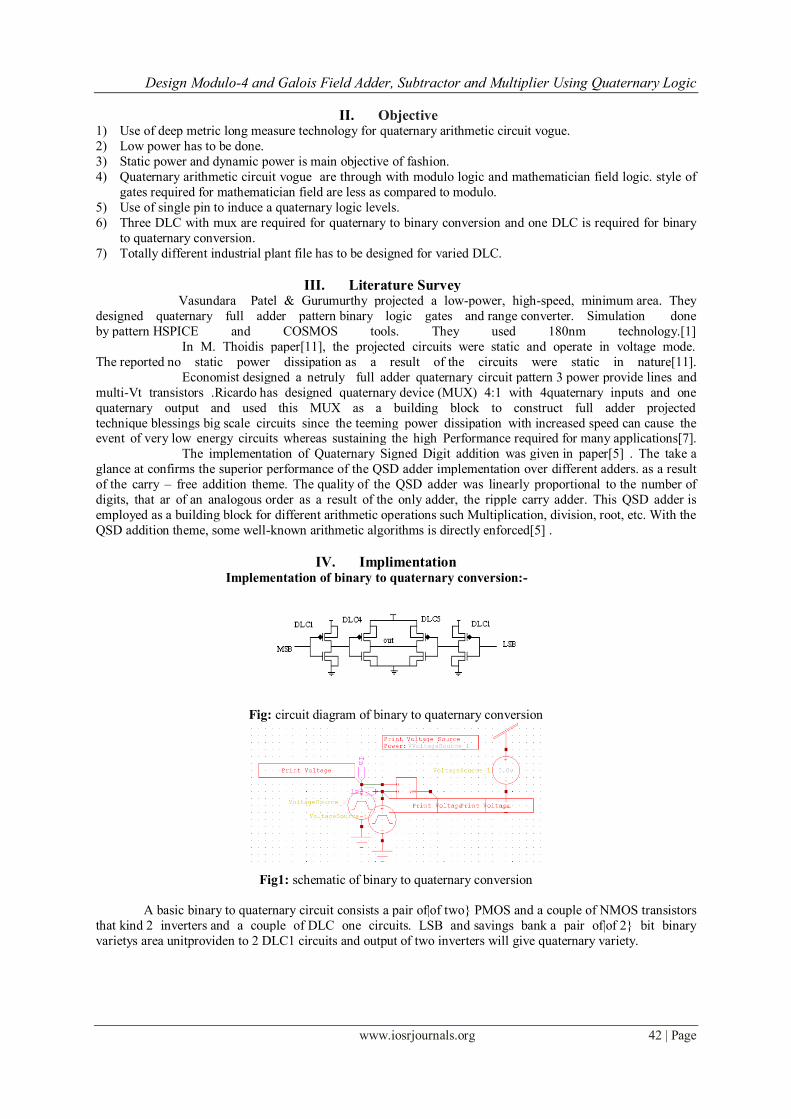
IV. Implimentation Implementation of binary to quaternary conversion:-
Fig: circuit diagram of binary to quaternary conversion
Fig1: schematic of binary to quaternary conversion
A basic binary to quaternary circuit consists a pair of|of two} PMOS and a couple of NMOS transistors
that kind 2 inverters and a couple of DLC one circuits. LSB and savings bank a pair of|of 2} bit binary
varietys area unitproviden to 2 DLC1 circuits and output of two inverters will give quaternary variety.
Design Modulo-4 and Galois Field Adder, Subtractor and Multiplier Using Quaternary Logic
www.iosrjournals.org 43 | Page
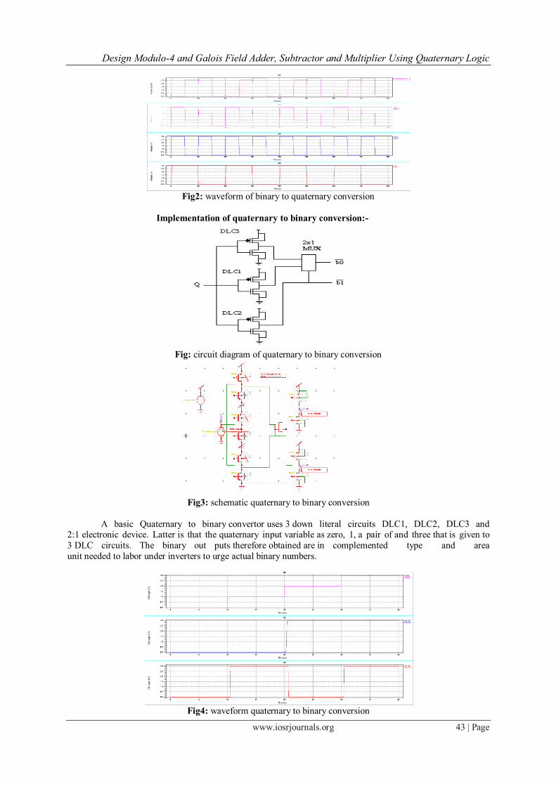
Fig2: waveform of binary to quaternary conversion
Implementation of quaternary to binary conversion:-
Fig: circuit diagram of quaternary to binary conversion
Fig3: schematic quaternary to binary conversion
A basic Quaternary to binary convertor uses 3 down literal circuits DLC1, DLC2, DLC3 and 2:1 electronic device. Latter is that the quaternary input variable as zero, 1, a pair of and three that is given to
3 DLC circuits. The binary out puts therefore obtained are in complemented type and area
unit needed to labor under inverters to urge actual binary numbers.
Fig4: waveform quaternary to binary conversion
Design Modulo-4 and Galois Field Adder, Subtractor and Multiplier Using Quaternary Logic
www.iosrjournals.org 44 | Page
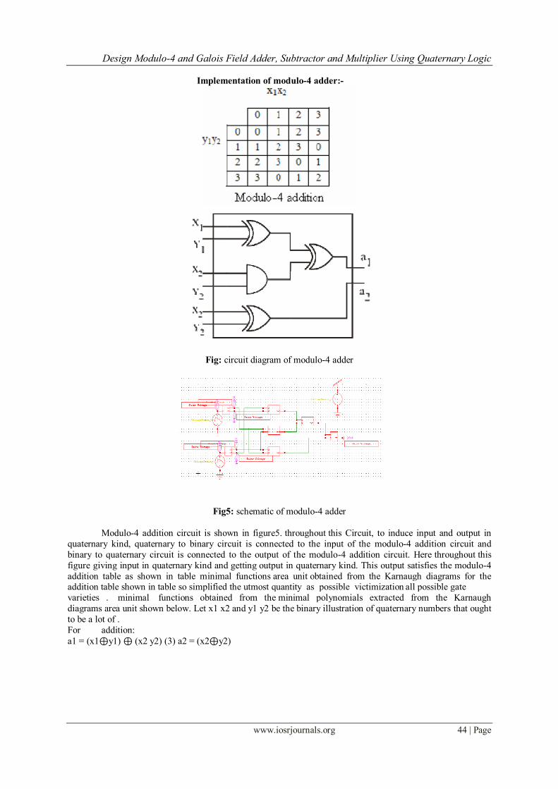
Implementation of modulo-4 adder:-
Fig: circuit diagram of modulo-4 adder
Fig5: schematic of modulo-4 adder
Modulo-4 addition circuit is shown in figure5. throughout this Circuit, to induce input and output in
quaternary kind, quaternary to binary circuit is connected to the input of the modulo-4 addition circuit and
binary to quaternary circuit is connected to the output of the modulo-4 addition circuit. Here throughout this
figure giving input in quaternary kind and getting output in quaternary kind. This output satisfies the modulo-4
addition table as shown in table minimal functions area unit obtained from the Karnaugh diagrams for the addition table shown in table so simplified the utmost quantity as possible victimization all possible gate
varieties . minimal functions obtained from the minimal polynomials extracted from the Karnaugh
diagrams area unit shown below. Let x1 x2 and y1 y2 be the binary illustration of quaternary numbers that ought
to be a lot of .
For addition:
a1 = (x1⊕y1) ⊕ (x2 y2) (3) a2 = (x2⊕y2)
Design Modulo-4 and Galois Field Adder, Subtractor and Multiplier Using Quaternary Logic
www.iosrjournals.org 45 | Page
Fig6: waveform of modulo-4 adder
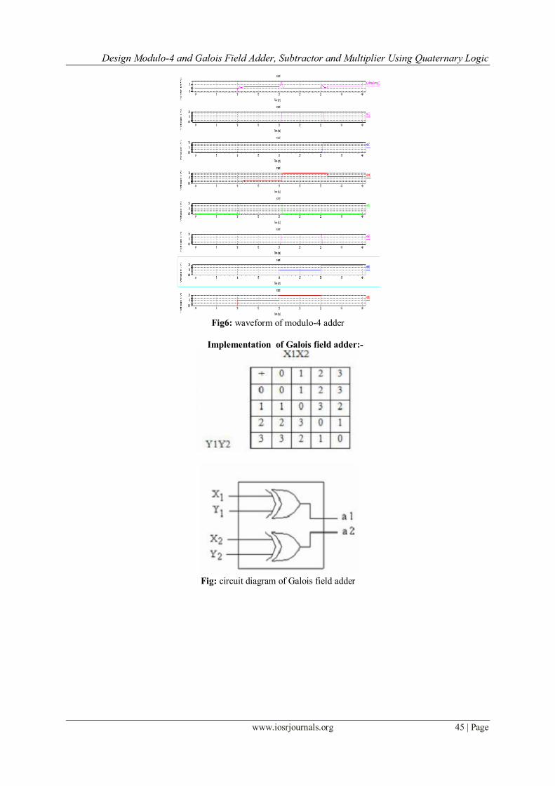
Implementation of Galois field adder:-
Fig: circuit diagram of Galois field adder
Design Modulo-4 and Galois Field Adder, Subtractor and Multiplier Using Quaternary Logic
www.iosrjournals.org 46 | Page
Fig7: schematic of Galois field adder
Galois addition table in Figure is utilized in Karnaugh diagrams to induce minimum operate. Stripped
functions obtained from the stripped polynomials extracted from the Karnaugh diagrams for GF (4) addition is shown below. Let x1 x2 and y1 y2 be the binary illustration of two quaternary numbers that have to be
compelled to be compelled to be accessorial. a 1 and a 2 square measure the two bit results of addition between
x1x2 and y1y2.
a1=(x1y1)
a2=(x2y2)
Above equation shows that addition in GF (4) needs solely 2 gates and depth of web is reduced to a
minimum of one. Usually this can be often a extremely smart vogue among four circuits. Logical
implementation of the circuit is shown in figure .
Fig8: waveform of Galois field adder
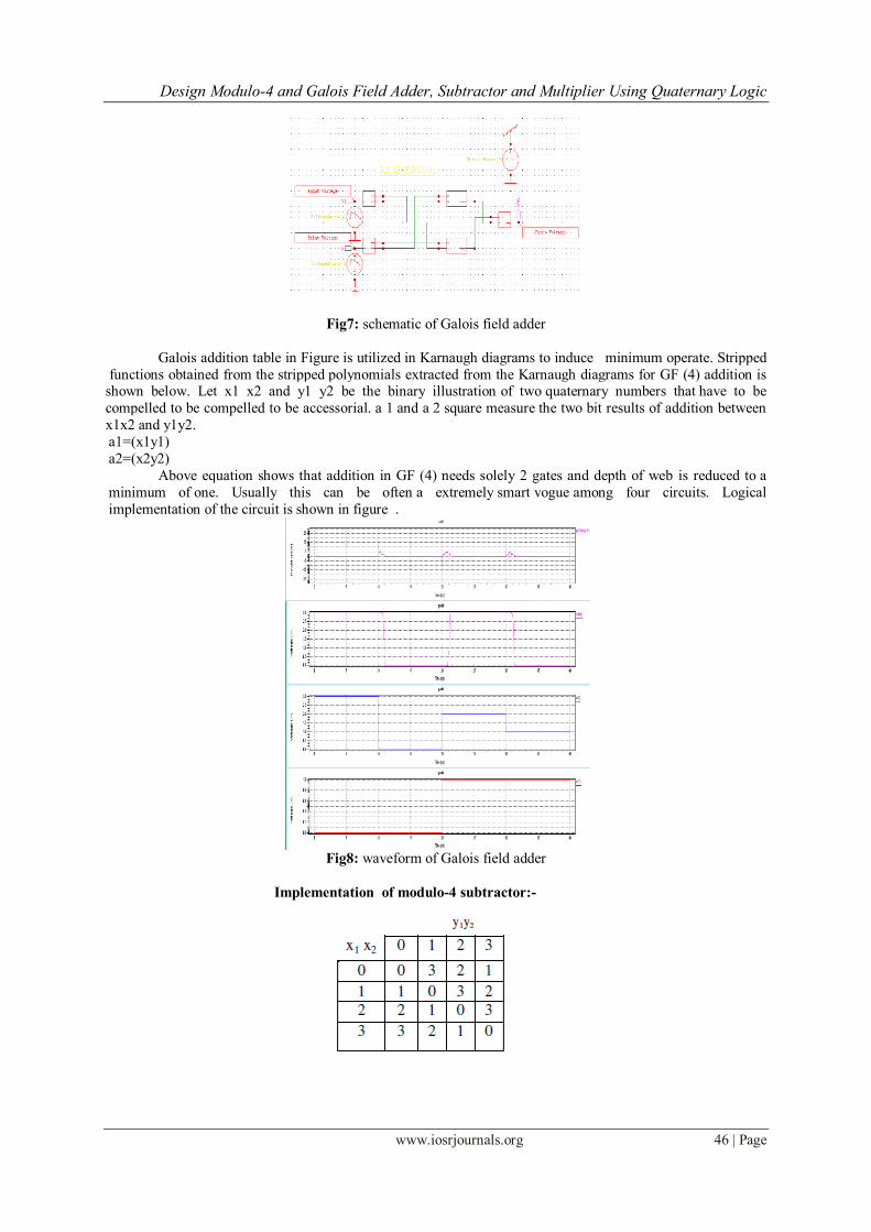
Implementation of modulo-4 subtractor:-
Design Modulo-4 and Galois Field Adder, Subtractor and Multiplier Using Quaternary Logic
www.iosrjournals.org 47 | Page
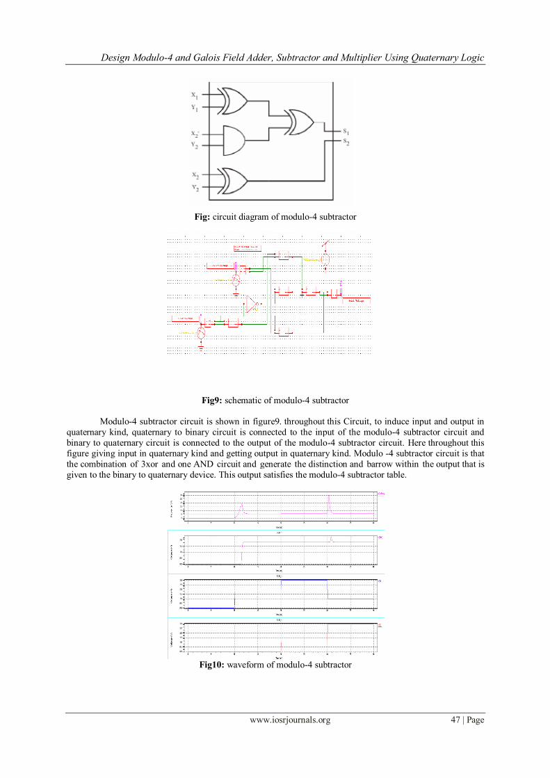
Fig: circuit diagram of modulo-4 subtractor
Fig9: schematic of modulo-4 subtractor
Modulo-4 subtractor circuit is shown in figure9. throughout this Circuit, to induce input and output in
quaternary kind, quaternary to binary circuit is connected to the input of the modulo-4 subtractor circuit and
binary to quaternary circuit is connected to the output of the modulo-4 subtractor circuit. Here throughout this
figure giving input in quaternary kind and getting output in quaternary kind. Modulo -4 subtractor circuit is that
the combination of 3xor and one AND circuit and generate the distinction and barrow within the output that is
given to the binary to quaternary device. This output satisfies the modulo-4 subtractor table.
Fig10: waveform of modulo-4 subtractor
Design Modulo-4 and Galois Field Adder, Subtractor and Multiplier Using Quaternary Logic
www.iosrjournals.org 48 | Page
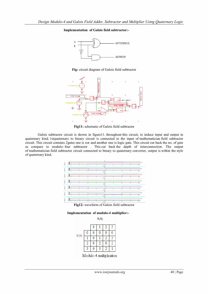
Implementation of Galois field subtractor:-
Fig: circuit diagram of Galois field subtractor
Fig11: schematic of Galois field subtractor
Galois subtractor circuit is shown in figure11. throughout this circuit, to induce input and output in
quaternary kind. 1stquaternary to binary circuit is connected to the input of mathematician field subtractor
circuit. This circuit contains 2gates one is xor and another one is logic gate. This circuit cut back the no. of gate
as compare to modulo- four subtractor . This cut back the depth of interconnection. The output
of mathematician field subtractor circuit connected to binary to quaternary converter, output is within the style of quaternary kind.
Fig12: waveform of Galois field subtractor
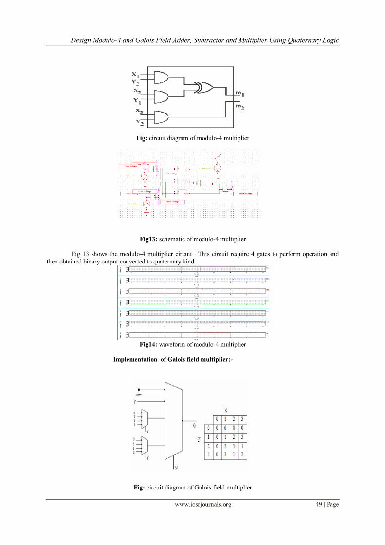
Implementation of modulo-4 multiplier:-
Design Modulo-4 and Galois Field Adder, Subtractor and Multiplier Using Quaternary Logic
www.iosrjournals.org 49 | Page
Fig: circuit diagram of modulo-4 multiplier
Fig13: schematic of modulo-4 multiplier
Fig 13 shows the modulo-4 multiplier circuit . This circuit require 4 gates to perform operation and
then obtained binary output converted to quaternary kind.
Fig14: waveform of modulo-4 multiplier
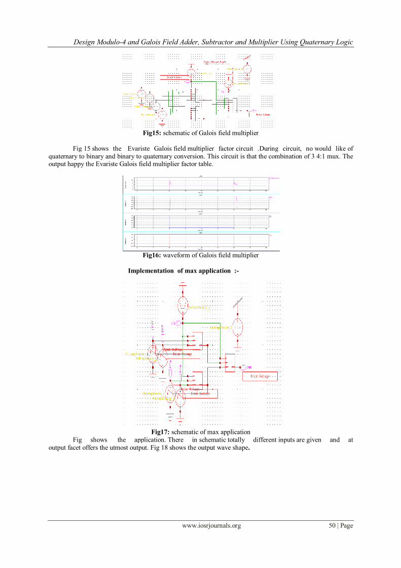
Implementation of Galois field multiplier:-
Fig: circuit diagram of Galois field multiplier
Design Modulo-4 and Galois Field Adder, Subtractor and Multiplier Using Quaternary Logic
www.iosrjournals.org 50 | Page
Fig15: schematic of Galois field multiplier
Fig 15 shows the Evariste Galois field multiplier factor circuit .During circuit, no would like of
quaternary to binary and binary to quaternary conversion. This circuit is that the combination of 3 4:1 mux. The output happy the Evariste Galois field multiplier factor table.
Fig16: waveform of Galois field multiplier
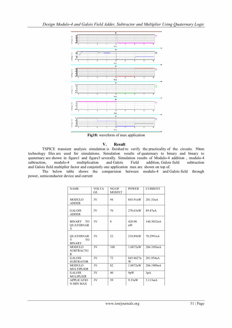
Implementation of max application :-
Fig17: schematic of max application
Fig shows the application. There in schematic totally different inputs are given and at
output facet offers the utmost output. Fig 18 shows the output wave shape.
Design Modulo-4 and Galois Field Adder, Subtractor and Multiplier Using Quaternary Logic
www.iosrjournals.org 51 | Page
Fig18: waveform of max application
V. Result TSPICE transient analysis simulation is finished to verify the practicality of the circuits. 50nm
technology files are used for simulations. Simulation results of quaternary to binary and binary to
quaternary are shown in figure1 and figure3 severally. Simulation results of Modulo-4 addition , modulo-4
subtraction, modulo-4 multiplication and Galois Field addition, Galois field subtraction
and Galois field multiplier factor and conjointly one application max are shown on top of.
The below table shows the comparision between modulo-4 and Galois field through
power, semiconductor device and current
NAME VOLTA
GE
NO.OF
MOSFET
POWER CURRENT
MODULO
ADDER
3V
94
845.91nW
281.33nA
GALOIS
ADDER
3V
76
270.63nW
89.47nA
BINARY TO
QUATERNAR
Y
3V
8
420.90
nW
140.3032nA
QUATERNAR
Y TO
BINARY
3V
22
210.89nW
70.2991nA
MODULO
SUBTRACTO
R
3V 108 1.0872uW 286.1056nA
GALOIS
SUBTRATOR
3V 72 845.8627n
W
281.954nA
MODULO
MULTIPLIER
3V 82 1.0872uW 286.1909nA
GALOIS
MULIPLIER
3V 40 9pW 3pA
APPLICATIO
N MIN MAX
3V 39 9.33nW 3.113mA
Design Modulo-4 and Galois Field Adder, Subtractor and Multiplier Using Quaternary Logic
www.iosrjournals.org 52 | Page
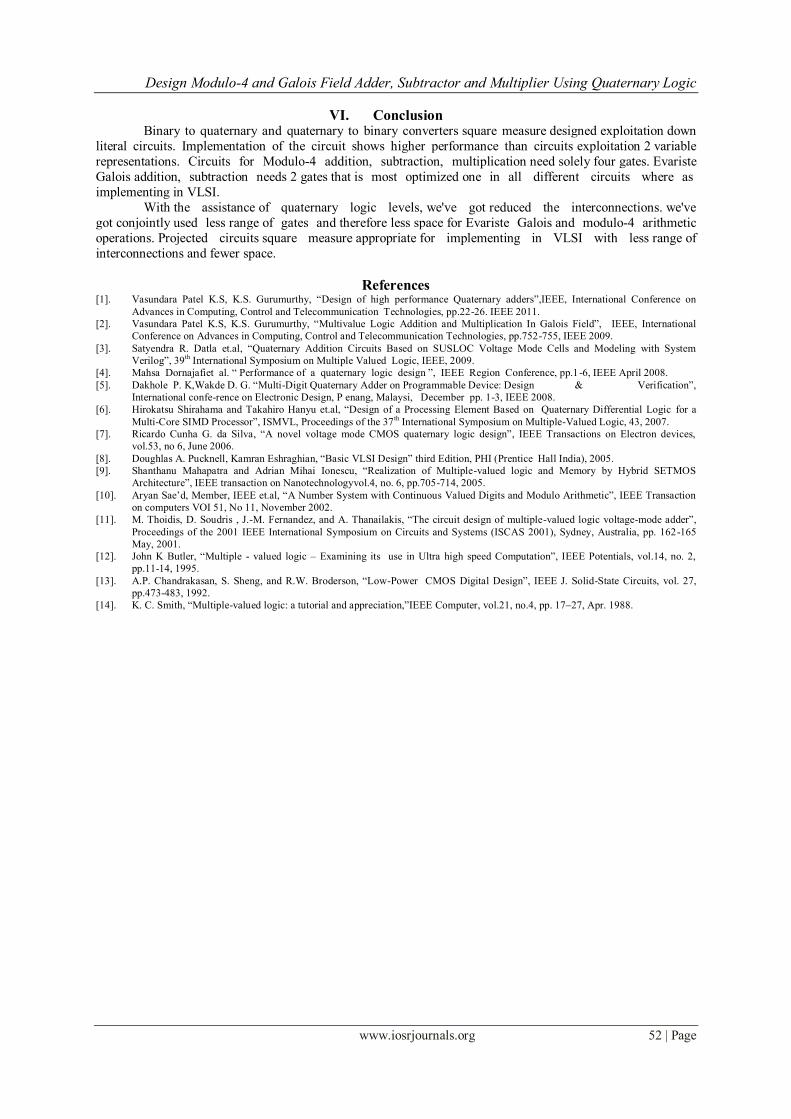
VI. Conclusion Binary to quaternary and quaternary to binary converters square measure designed exploitation down
literal circuits. Implementation of the circuit shows higher performance than circuits exploitation 2 variable
representations. Circuits for Modulo-4 addition, subtraction, multiplication need solely four gates. Evariste
Galois addition, subtraction needs 2 gates that is most optimized one in all different circuits where as
implementing in VLSI.
With the assistance of quaternary logic levels, we've got reduced the interconnections. we've
got conjointly used less range of gates and therefore less space for Evariste Galois and modulo-4 arithmetic
operations. Projected circuits square measure appropriate for implementing in VLSI with less range of
interconnections and fewer space.
References [1]. Vasundara Patel K.S, K.S. Gurumurthy, “Design of high performance Quaternary adders”,IEEE, International Conference on
Advances in Computing, Control and Telecommunication Technologies, pp.22-26. IEEE 2011.
[2]. Vasundara Patel K.S, K.S. Gurumurthy, “Multivalue Logic Addition and Multiplication In Galois Field”, IEEE, International
Conference on Advances in Computing, Control and Telecommunication Technologies, pp.752-755, IEEE 2009.
[3]. Satyendra R. Datla et.al, “Quaternary Addition Circuits Based on SUSLOC Voltage Mode Cells and Modeling with System
Verilog”, 39th International Symposium on Multiple Valued Logic, IEEE, 2009.
[4]. Mahsa Dornajafiet al. “ Performance of a quaternary logic design ”, IEEE Region Conference, pp.1 -6, IEEE April 2008.
[5]. Dakhole P. K,Wakde D. G. “Multi-Digit Quaternary Adder on Programmable Device: Design & Verification”,
International confe-rence on Electronic Design, P enang, Malaysi, December pp. 1-3, IEEE 2008.
[6]. Hirokatsu Shirahama and Takahiro Hanyu et.al, “Design of a Processing Element Based on Quaternary Differential Logic for a
Multi-Core SIMD Processor”, ISMVL, Proceedings of the 37th International Symposium on Multiple-Valued Logic, 43, 2007.
[7]. Ricardo Cunha G. da Silva, “A novel voltage mode CMOS quaternary logic design”, IEEE Transactions on Electron devices,
vol.53, no 6, June 2006.
[8]. Doughlas A. Pucknell, Kamran Eshraghian, “Basic VLSI Design” third Edition, PHI (Prentice Hall India), 2005.
[9]. Shanthanu Mahapatra and Adrian Mihai Ionescu, “Realization of Multiple-valued logic and Memory by Hybrid SETMOS
Architecture”, IEEE transaction on Nanotechnologyvol.4, no. 6, pp.705-714, 2005.
[10]. Aryan Sae’d, Member, IEEE et.al, “A Number System with Continuous Valued Digits and Modulo Arithmetic”, IEEE Transaction
on computers VOI 51, No 11, November 2002.
[11]. M. Thoidis, D. Soudris , J.-M. Fernandez, and A. Thanailakis, “The circuit design of multiple-valued logic voltage-mode adder”,
Proceedings of the 2001 IEEE International Symposium on Circuits and Systems (ISCAS 2001), Sydney, Australia, pp. 162-165
May, 2001.
[12]. John K Butler, “Multiple - valued logic – Examining its use in Ultra high speed Computation”, IEEE Potentials, vol.14, no. 2,
pp.11-14, 1995.
[13]. A.P. Chandrakasan, S. Sheng, and R.W. Broderson, “Low-Power CMOS Digital Design”, IEEE J. Solid-State Circuits, vol. 27,
pp.473-483, 1992.
[14]. K. C. Smith, “Multiple-valued logic: a tutorial and appreciation,”IEEE Computer, vol.21, no.4, pp. 17–27, Apr. 1988.