Design, Manufacturing, and Assembly of a Flexible ...
201
University of South Florida Scholar Commons Graduate eses and Dissertations Graduate School January 2013 Design, Manufacturing, and Assembly of a Flexible ermoelectric Device Christopher Anthony Martinez University of South Florida, [email protected] Follow this and additional works at: hp://scholarcommons.usf.edu/etd Part of the Electrical and Computer Engineering Commons , Mechanical Engineering Commons , and the Neurosciences Commons is esis is brought to you for free and open access by the Graduate School at Scholar Commons. It has been accepted for inclusion in Graduate eses and Dissertations by an authorized administrator of Scholar Commons. For more information, please contact [email protected]. Scholar Commons Citation Martinez, Christopher Anthony, "Design, Manufacturing, and Assembly of a Flexible ermoelectric Device" (2013). Graduate eses and Dissertations. hp://scholarcommons.usf.edu/etd/4723
Transcript of Design, Manufacturing, and Assembly of a Flexible ...

University of South FloridaScholar Commons
Graduate Theses and Dissertations Graduate School
January 2013
Design, Manufacturing, and Assembly of a FlexibleThermoelectric DeviceChristopher Anthony MartinezUniversity of South Florida, [email protected]
Follow this and additional works at: http://scholarcommons.usf.edu/etd
Part of the Electrical and Computer Engineering Commons, Mechanical Engineering Commons,and the Neurosciences Commons
This Thesis is brought to you for free and open access by the Graduate School at Scholar Commons. It has been accepted for inclusion in GraduateTheses and Dissertations by an authorized administrator of Scholar Commons. For more information, please contact [email protected].
Scholar Commons CitationMartinez, Christopher Anthony, "Design, Manufacturing, and Assembly of a Flexible Thermoelectric Device" (2013). Graduate Thesesand Dissertations.http://scholarcommons.usf.edu/etd/4723

Design, Manufacturing, and Assembly of a Flexible Thermoelectric Device
by
Christopher Martinez
A thesis submitted in partial fulfillment of the requirements for the degree of
Master of Science in Mechanical Engineering Department of Mechanical Engineering
College of Engineering University of South Florida
Major Professor: Nathan Crane, Ph.D. Kyle Reed, Ph.D.
Frank Pyrtle, Ph.D.
Date of Approval: June 29, 2013
Keywords: thermoelement, circuit board, heat transfer, scalable, design for assembly
Copyright © 2013, Christopher Martinez

DEDICATION
I dedicate this thesis to the self-made individual, the personal pioneer who
elevates their standings to a position far removed from where they originated.

ACKNOWLEDGMENTS
I would like to thank Dr. Nathan Crane for extending his guidance, ingenuity, and
patience with me on this project. It was through Dr. Crane that I began research as an
undergraduate here at USF and it is under his mentorship that I conclude it as a
graduate student.
I would also like to thank Dr. Kyle Reed for his support. Dr. Reed’s
troubleshooting assistance during the control system portion of the research was time
spent that this thesis cannot lay testament to.
The University of South Florida and their Mechanical Engineering department
have been tremendously helpful to me during my academic career. Without the college’s
resources, professors, faculty, and staff this thesis would not be possible.
Lastly, I would like to thank those who have made the longest and largest
contributions toward my success, my family and friends. I owe thanks to my mother
Frances Martinez for her endless encouragement and faith in my abilities, my brother
Joseph Martinez, my sister-in-law Ellen Martinez, my cousin Jeffery Sawick, my aunt
Elizabeth Reiff, and my soon to be mother-in-law Sandi Kahn all of whom expressed
interest which reinvigorated my own, and my fiancé Julie Kahn for her tireless support.
Thank you also to my friend Yohannes Samuel, my lab mates Jose Carballo, Benjamin
Hahne, and Qi Ni for providing help in their areas of expertise, and Brian Bertram for his
help while I was an undergraduate.
This work was funded in part by support from the National Science Foundation
through grant CMMI-0927637.

i
TABLE OF CONTENTS
LIST OF TABLES ........................................................................................................... iv LIST OF FIGURES ......................................................................................................... vi ABSTRACT .................................................................................................................. xiii CHAPTER ONE: INTRODUCTION ................................................................................ 1
Motivation ........................................................................................................... 1 Previous Work .................................................................................................... 2 Conceptual Background ...................................................................................... 4 Thermoelectric Materials ..................................................................................... 6 Outline ................................................................................................................ 8
CHAPTER TWO: THERMOELECTRIC DEVICE DESIGN .............................................10
Environmental Parameters .................................................................................10 Device Requirements .........................................................................................10 Device Modeling ................................................................................................11
Modeling Conclusions ............................................................................17 Forearm Modeling ..............................................................................................18 Component Attachment .....................................................................................20
Temperature Sensors .............................................................................23 Materials ............................................................................................................24
Thermoelectric Elements ........................................................................24 Substrate Material ..................................................................................25 Solder Paste ...........................................................................................26
Circuit Boards ....................................................................................................27 Adjusted Performance Estimates ...........................................................30 Design for Assembly ..............................................................................31 Optimizing Preprocessing Design ...........................................................36
Staging Area ......................................................................................................38 CHAPTER THREE: MANUFACTURING .......................................................................41
Manufacturing Process Overview .......................................................................41 Procedures ........................................................................................................42
Etching Procedure ..................................................................................42 Milling Procedure ....................................................................................44
Preliminary Etching Tests ..................................................................................46 Solder Stencil Etching ............................................................................46 Circuit Board Etching ..............................................................................48
Preliminary Milling Tests ....................................................................................53 Solder Stencil Milling ..............................................................................53 Thermoelement Template Milling ...........................................................60 Staging Area ..........................................................................................61

ii
Final Component Results ...................................................................................61 Circuit Boards .........................................................................................61 Solder Stencil .........................................................................................64 Thermoelement Templates .....................................................................65
CHAPTER FOUR: ASSEMBLY .....................................................................................68
Steps .................................................................................................................68 Trial Assembly Results and Discussion ..............................................................77
Trial Assembly Motivation .......................................................................77 Post Processing Difficulty .......................................................................81 Final Assembly Results and Discussion .................................................81
Closing Remarks................................................................................................83 CHAPTER FIVE: DEVICE PERFORMANCE .................................................................85
Testing Methods ................................................................................................85 Data Acquisition .....................................................................................85 Temperature Sensor Calibration .............................................................86 System Arrangement ..............................................................................87
Performance Data ..............................................................................................90 Analysis of a Single Sensor across a Range of Amperages ...................90 Analysis of a Single Sensor across a Range of Channels ......................91 Analysis of a Single Channel at a Constant Amperage ...........................92 Calculated Time Constants.....................................................................93
Comparison with the 1-D Model .........................................................................94 Results Comparison with the Initial 1-D Model .......................................94 Results Comparison with a 1-D Model Reflecting Final Design ..............95
Calculated Seebeck Coefficient .........................................................................97 Testing Procedure Errors ...................................................................................98
Alternative Arrangement for Bottom Temperature Sensors .................. 101 Adequacy of Performance ................................................................................ 102
CHAPTER SIX: CONCLUSIONS AND FUTURE WORK ............................................. 103
Design Conclusions ......................................................................................... 103 Sources of Design Error ....................................................................... 104 Future Work for the Design .................................................................. 104
Manufacturing Conclusions .............................................................................. 104 Sources of Manufacturing Error ............................................................ 105 Future Work for the Manufacturing Process ......................................... 107
Assembly Conclusion ....................................................................................... 107 Sources of Assembly Error ................................................................... 108 Future Work for the Assembly Process ................................................ 108
Performance Conclusions ................................................................................ 108 Sources of Performance Error .............................................................. 108
Conclusion ....................................................................................................... 109 REFERENCES ............................................................................................................ 111 APPENDICES ............................................................................................................. 114
Appendix A: 1D Model MATLAB Code ............................................................. 115 Appendix B: Human Heat Flux Calculations ..................................................... 118 Appendix C: MATLAB Gcode Generator .......................................................... 119

iii
Appendix D: Stencil and Middle Template Gcode ............................................ 126 Appendix E: System Wiring Diagram ............................................................... 153 Appendix F: Control System MATLAB Code .................................................... 156 Appendix G: MATLAB Temperature Sensor Measurement Code ..................... 163 Appendix H: Measured Temperature Profiles of the Final Assembly ................ 165
H.1 Purple Channel .............................................................................. 165 H.2 Yellow Channel .............................................................................. 170 H.3 Blue Channel ................................................................................. 175 H.4 Green Channel .............................................................................. 180
iv
LIST OF TABLES
Table 1: Thermoelements and their temperature specific performance .................. 7
Table 2: Values of assumed modeling parameters ............................................... 14
Table 3: Preliminary estimates for thermoelement performance ........................... 15
Table 4: P-type bismuth telluride properties ......................................................... 25
Table 5: Bismuth telluride properties used in the preliminary 1-D model .............. 25
Table 6: Material properties of the flexible circuit board ........................................ 26
Table 7: Preliminary board dimensions used for alignment and cost optimization ............................................................................................ 36
Table 8: Material properties of 2046-T6 aluminum alloy ....................................... 38
Table 9: Time and temperature profile for the first full scale solder reflow attempt ................................................................................................... 82
Table 10: Time and temperature profile for the second full scale solder reflow attempt ......................................................................................... 82
Table 11: Hot temperature exposure for sensor calibration .................................... 86
Table 12: Cold temperature exposure for sensor calibration .................................. 86
Table 13: Temperature sensor constants for resistance to temperature conversion .............................................................................................. 87
Table 14 Averaged area and amperage specific time constants ........................... 94
Table 15: Numerical comparison between predicted temperatures from the 1-D model and the experimental values obtained from the underside center of the purple channel ................................................... 94
Table 16: Numerical comparison between estimated temperatures from the updated 1-D model and the experimental values obtained from the underside center of the purple channel ................................................... 95
Table 17: Updated 1-D model’s peak magnitudes .................................................. 96
Table 18: Voltages of each channel when the outermost hot and cold side device surfaces are at 31 and 8 °C ......................................................... 97

v
Table 19: Updated 1-D model temperature inputs and corresponding zero amperage thermoelement surface temperatures .................................... 98
Table 20: Difference between temperature sensor’s value and the temperature obtained by the temperature probe used for calibration ............................................................................................... 99
Table 21: Result comparison between the project requirements and those achieved ............................................................................................... 109
Table A: Human heat flux calculations using the Fiala et al model ...................... 118

vi
LIST OF FIGURES
Figure 1: Simple thermoelectric circuit .................................................................... 4
Figure 2: Heat flow through a column based thermoelectric circuit ......................... 6
Figure 3: 1-D locations of thermal resistance and their contribution to the model .....................................................................................................15
Figure 4: 1-D heat transfer model’s estimated thermal fluxes for each surface ...................................................................................................16
Figure 5: 1-D heat transfer model’s estimated temperatures for each surface ...................................................................................................17
Figure 6: Example of a side view of a column based arrangement of thermoelements mounted perpendicularly to electrically conductive material ................................................................................18
Figure 7: Diagram of intended through hole pin placement to circuit board placement and mating surfaces ..............................................................21
Figure 8: Example of a through hole mounted electrical component soldered to a circuit board on the side opposite its insertion .................................21
Figure 9: Example of a solder pad mounting arrangement: component, solder pads, and circuit board surface ....................................................22
Figure 10: Example of solder joints created by reflowing the solder of the assemble post part placement ................................................................22
Figure 11: Problems resulting from uneven solder pads ..........................................23
Figure 12: Bottom TE circuit traces with designated areas for temp sensor placement ...............................................................................................28
Figure 13: Gap, trace segment, and temperature sensor dimensions for the bottom circuit board ................................................................................28
Figure 14: Dark squares represent the locations of the 180 thermoelement blocks on the 5 channels of the bottom circuit board ..............................29
Figure 15: Upper TE circuit traces ...........................................................................29
Figure 16: Dimensions used when calculating the fill factor .....................................30
Figure 17: Top and bottom circuit boards with alignment tabs .................................32

vii
Figure 18: Visual representation of Equation 32 ......................................................33
Figure 19: Dimension notation for the preprocessed circuit board ...........................34
Figure 20: Demonstrated benefit of asymmetric preprocessing circuit board design ....................................................................................................35
Figure 21: Alignment improvement and normalized tab area both as functions of ...................................................................................................37
Figure 22: Staging area assembly view from multiple perspectives and dimensioned ...........................................................................................39
Figure 23: Full scale staging area manufactured by the University of South Florida machine shop .............................................................................40
Figure 24: Mock example of ironing arrangement for ink transference to brass or copper ......................................................................................43
Figure 25: Picture and labels of the mill assembly ...................................................46
Figure 26: First etched sample – Brass trial solder stencil .......................................47
Figure 27: Deposited solder using the first brass stencil ..........................................47
Figure 28: Negative image for the transparency of the second etched solder stencil .....................................................................................................48
Figure 29: Second etched brass solder stencil ........................................................48
Figure 30: Negative image for the transparency of the first trial assembly ...............49
Figure 31: Etched results for the first trial assembly ................................................49
Figure 32: Negative image for the transparency of the second trial assembly .........50
Figure 33: Etched results for the second trial assembly ...........................................50
Figure 34: Negative image for the transparency of the third trial assembly ..............51
Figure 35: Etched results for the third trial assembly ...............................................51
Figure 36: Negative image for the transparency of the fourth trial assembly and the intended cutting wheel path .......................................................52
Figure 37: 2mm and 1mm aperture milled solder stencils ........................................53
Figure 38: 1mm and 2 mm apertures, solder reflow at 180 °C .................................54
Figure 39: Two samples of the 1 mm aperture, solder reflow at 190 °C ...................55
Figure 40: Two samples of the 2 mm aperture solder reflow at 190 °C ....................55
Figure 41: Two samples of the 1 mm aperture solder reflow at 200 °C ....................56

viii
Figure 42: Two samples of the 2 mm aperture solder reflow at 200 °C ....................56
Figure 43: Top view of solder reflow results from different temperature exposures and stencil (1mm and 2mm) uses .........................................57
Figure 44: Profile picture taken of the first trial assembly to analyze solder joint quality .............................................................................................58
Figure 45: Framed 2 mm solder stencil ...................................................................59
Figure 46: Transparency based solder stencil used on third and fourth trial assemblies .............................................................................................59
Figure 47: Brass thermoelement alignment templates for the third and fourth trial assemblies.......................................................................................60
Figure 48: Trial assembly stage with a stainless steel base and two 1/4 x 20 x 3 studs. ................................................................................................61
Figure 49: Gap and trace dimensions for the bottom circuit board etch mask ..........62
Figure 50: Bottom circuit board etching mask ..........................................................62
Figure 51: Post etching bottom (1) and top (2) circuit boards for the full scale assembly ................................................................................................63
Figure 52: Automated pathway preview of the mill’s cutting tool for the full scale transparency based solder stencil .................................................64
Figure 53: Transparency based solder stencil for the full scale assembly ................65
Figure 54: Automated pathway preview of the mill’s cutting tool for the full scale bottom thermoelement template ....................................................66
Figure 55: Automated pathway preview of the mill’s cutting tool for the full scale middle thermoelement template ....................................................66
Figure 56: Automated pathway preview of the mill’s cutting tool for the full scale top thermoelement template ..........................................................66
Figure 57: Finished full scale thermoelement templates ..........................................67
Figure 58: Schematic of solder paste application process .......................................69
Figure 59: Solder stencil on top of the top circuit board prior to solder paste application ..............................................................................................70
Figure 60: Schematic of the post solder paste application results............................70
Figure 61: Top circuit board after successful solder paste application .....................71
Figure 62: Bottom circuit board after successful solder paste application ................71

ix
Figure 63: Schematic of the thermoelement and thermoelement template application process .................................................................................73
Figure 64: Bottom, middle, and top thermoelement templates applied to the bottom circuit board ................................................................................74
Figure 65: Top thermoelement template removed after p-type thermoelements are positioned ..............................................................75
Figure 66: Remaining thermoelement templates removed after n-type thermoelements are positioned ..............................................................75
Figure 67: Close up of the thermoelements positioned on the bottom circuit board ......................................................................................................75
Figure 68: Schematic of the top circuit board placed on top of the thermoelements ......................................................................................76
Figure 69: Assembled circuit boards with thermoelement templates and mill restraints used as weights for the reflow process ...................................76
Figure 70: Schematic of the post processing circuit board .......................................77
Figure 71: Actual post processing circuit board with wires attached ........................77
Figure 72: Top view of the first trial assembly ..........................................................78
Figure 73: Top view of the second trial assembly ....................................................78
Figure 74: Top view of the third trial assembly.........................................................79
Figure 75: Top view of the fourth (final) trial assembly .............................................80
Figure 76: Transparent superposition of the fourth trial assembly on top of the third trial assembly ............................................................................80
Figure 77: Comparison between temperature profiles of the solder reflow attempts .................................................................................................83
Figure 78: Water bottle with bottom sensors attached .............................................88
Figure 79: TE device with sensors on both its underside and topside ......................88
Figure 80: Complete TE device testing arrangement ...............................................89
Figure 81: Description of channel notation on the TE device ...................................90
Figure 82: Center underside sensor’s measurement of temperature change when varying amperage on the purple channel ......................................91
Figure 83: Left underside sensor’s measurement of temperature change at different channels for 2.5 A .....................................................................92
x
Figure 84: Temperature changes at different locations of the green channel at 2.5 A ...................................................................................................93
Figure 85: Comparison between actual results, initial theoretical 1-D estimates, and estimates from the updated 1-D model ...........................96
Figure 86: Cooling flux comparison between the initial 1-D model and the updated 1-D model which better reflects the final design’s materials and dimensions .......................................................................96
Figure 87: Measured response of each temperature sensor being placed in between my thumb and index fingers. .................................................. 100
Figure 88: Development of a contact angle between the TE device and the bottom reservoir ................................................................................... 101
Figure 89: Sensor mounting alternative to tape ..................................................... 102
Figure 90: Graphical datum analysis used for determining maximum and minimum differences from a specific trace segment within the channel ................................................................................................ 105
Figure 91: Comparison between the apertures of the full scale assembly’s solder stencil (left) and the trial assembly’s (right) ................................ 106
Figure 92: Intended solder pad profile (left) and an example of the hypothesized solder pad profile (right) produced by the full scale assembly’s solder stencil ...................................................................... 107
Figure A: Wiring diagram describing how power is supplied to the different channels (Supply for channels 0, 1, 2, and 3), and how the information is relayed to the Phidget P/N 1002 board ........................... 153
Figure B: Wiring diagram describing how power is supplied to the different temperature sensor boards (sensors 0, 1, 2, 4, and 5), and how the information is relayed to the Phidget 8/8/8 board ............................ 154
Figure C: Trace diagram for the temperature sensor circuit boards ...................... 155
Figure D: Underside purple channel temperature profile at 0.5 amps ................... 165
Figure E: Topside purple channel temperature profile at 0.5 amps ...................... 165
Figure F: Underside purple channel temperature profile at 1.0 amps ................... 166
Figure G: Topside purple channel temperature profile at 1.0 amps ...................... 166
Figure H: Underside purple channel temperature profile at 1.5 amps ................... 167
Figure I: Topside purple channel temperature profile at 1.5 amps ...................... 167
Figure J: Underside purple channel temperature profile at 2.0 amps ................... 168
xi
Figure K: Topside purple channel temperature profile at 2.0 amps ...................... 168
Figure L: Underside purple channel temperature profile at 2.5 amps ................... 169
Figure M: Topside purple channel temperature profile at 2.5 amps ...................... 169
Figure N: Underside yellow channel temperature profile at 0.5 amps ................... 170
Figure O: Topside yellow channel temperature profile at 0.5 amps ...................... 170
Figure P: Underside yellow channel temperature profile at 1.0 amps ................... 171
Figure Q: Topside yellow channel temperature profile at 1.0 amps ...................... 171
Figure R: Underside yellow channel temperature profile at 1.5 amps ................... 172
Figure S: Topside yellow channel temperature profile at 1.5 amps ...................... 172
Figure T: Underside yellow channel temperature profile at 2.0 amps ................... 173
Figure U: Topside yellow channel temperature profile at 2.0 amps ...................... 173
Figure V: Underside yellow channel temperature profile at 2.5 amps ................... 174
Figure W: Topside yellow channel temperature profile at 2.5 amps ...................... 174
Figure X: Underside blue channel temperature profile at 0.5 amps ...................... 175
Figure Y: Topside blue channel temperature profile at 0.5 amps ......................... 175
Figure Z: Underside blue channel temperature profile at 1.0 amps ...................... 176
Figure AA: Topside blue channel temperature profile at 1.0 amps ......................... 176
Figure BB: Underside blue channel temperature profile at 1.5 amps ...................... 177
Figure CC: Topside blue channel temperature profile at 1.5 amps ......................... 177
Figure DD: Underside blue channel temperature profile at 2.0 amps ...................... 178
Figure EE: Topside blue channel temperature profile at 2.0 amps ......................... 178
Figure FF: Underside blue channel temperature profile at 2.5 amps ...................... 179
Figure GG: Topside blue channel temperature profile at 2.5 amps ......................... 179
Figure HH: Underside green channel temperature profile at 0.5 amps ................... 180
Figure II: Topside green channel temperature profile at 0.5 amps ....................... 180
Figure JJ: Underside green channel temperature profile at 1.0 amps ................... 181
Figure KK: Topside green channel temperature profile at 1.0 amps ....................... 181

xii
Figure LL: Underside green channel temperature profile at 1.5 amps ................... 182
Figure MM: Topside green channel temperature profile at 1.5 amps ....................... 182
Figure NN: Underside green channel temperature profile at 2.0 amps ................... 183
Figure OO: Topside green channel temperature profile at 2.0 amps ....................... 183
Figure PP: Underside green channel temperature profile at 2.5 amps ................... 184
Figure QQ: Topside green channel temperature profile at 2.5 amps ....................... 184

xiii
ABSTRACT
This thesis documents the design, manufacturing, and assembly of a flexible
thermoelectric device. Such a device has immediate use in haptics, medical, and athletic
applications. The governing theory behind the device is explained and a one
dimensional heat transfer model is developed to estimate performance. This model and
consideration for the manufacturing and assembly possibilities are the drivers behind the
decisions made in design choices. Once the design was finalized, manufacturing
methods for the various components were explored. The system was created by etching
copper patterns on a copper/polyimide laminate and screen printing solder paste onto
the circuits. Thermoelectric elements were manually assembled. Several proof of
concept prototypes were made to validate the approach. Development of the assembly
process also involved proof of concept prototyping and partial assembly analysis. A full
scale device was produced and tested to assess its thermoelectric behavior. The
resulting performance was an interface temperature drop of 3 °C in 10 seconds with 1.5
A supplied, and a maximum temperature drop of 9.9 °C after 2 minutes with 2.5 A
supplied. While the measured behavior fell short of predictions, it appears to be
adequate for the intended purpose. The differences appear to be due to larger than
expected thermal resistances between the device and the heat sinks and some possible
degradation of the thermoelectric elements due to excess solder coating the edges.

1
CHAPTER ONE: INTRODUCTION
Motivation
The purpose of this research is to design a flexible (bending diameter of 2 inches
about a single axis) and wearable (currently as a scientific instrument but with future
alternatives as an accessory or integrated into apparel) thermoelectric device (TED) that
can achieve a 15 °F temperature change within 10 seconds at different longitudinal
sections of the human to device interface. Since the device will be worn, the current
carrying surfaces must be isolated, and it must present no potential danger to the user.
This design must also allow for iteration based scalability (can increase or decrease the
device’s blanketing area) and adaptability (modifications can be made to accommodate
different power sources, heat sources, heat sinks, and performance metrics).
The immediate application of this device (at the time of writing) is to study the
human perception of multiple dynamic temperature inputs over small and large areas of
the body. Part of our study will involve safe investigation of the ‘thermal grill illusion’.
Discovered in 1896 by Torsten Thunberg, the ‘thermal grill illusion’ involves the
production of a burning sensation when warm (T 104 °F) and cold (T 68 °F)
temperature sources are paired within close proximity and applied to the human body.
[1] A better comprehension of the underlying physiological causes for this response
would improve the scientific community’s understanding on the operation of the
ventrolateral spinothalamic tract; which “mediates the perception of pain and
temperature.” [2]

2
However, this device has the potential to be used for more than misdirecting an
individual’s sensory perception. It could be used in athletics or other activities that
involve extensive physical exertion. In these scenarios, the device would provide cooling
for the individual, attenuating the onset of thermal fatigue. Stanford University is
currently developing a “cooling glove” for this purpose. For their design, participants
wear a multilayered glove which has cooled water circulated through its envelope. [3]
A derivative of this device could also be used in the examination of people
suffering from nerve damage, like that of painful diabetic neuropathy (PDN). Currently
electrophysiological procedures are capable of exploring the condition of large neural
fibers, those which perceive touch and proprioception. However, these procedures do
not analyze the smaller neural fibers, those which are sensitive to cold and hot
stimulation, and pain. These smaller fibers are first affected by the disease which then
progresses to the larger ones. [4] The temperature resolution this device is capable of
producing is proportional to the incremental change of electric current supplied.
Therefore it is plausible to use this device in an examination process where the
physician records the patient’s responses to various temperatures achieved with a high
level of precision.
Previous Work
This research is directly inspired by Patrick McKnight’s work in his thesis “Finite
element analysis of thermoelectric systems with applications in self assembly and
haptics.” In Chapter 4 – Thermal Haptic Display, Mr. McKnight discusses the creation of
a thermoelectric device that can create multiple temperatures along a series of
independent pathways where each of these pathways share a common control surface
that is in contact with human skin. He outlined a control system for the device and

3
developed a thermoelectric prototype that was able to successfully heat one side of the
device to 42 °C (108 °F). [5]
At the time of this publication there are few research articles relating to the
keywords “flexible thermoelectric cooler”. This may be due in part to the 2001 U.S.
patent on such devices. [6] This patent covers flexible column based single and multi-
layer TE devices where the flexibility is often suggested to be achieved by cutting the
circuit board and weakening it. The author does say frequently however that at least one
of the circuit boards must be rigid.
In 2008 researchers in Taiwan investigated the development of low cost rigid
micro scale thermoelectric coolers. Fabrication was completed using
microelectromechanical systems (MEMS) and two different methods for structuring the
thermoelements were applied. The first was a column based arrangement that used
bismuth telluride and bismuth antimonide elements. The alternative arrangement was a
“bridge type” structure; where polysilicon thermoelements and conductive metal were
interwoven in a crosshatched pattern. The authors concluded that their bridge type
assembly, with 62,500 elements covering a 100 mm2 chip yielded the best results; with a
2 °F temperature difference achieved by a 200 mA driving current. However, both of
their configurations required multiple photomasks (4 for the column type, 5 for the bridge
type), and the bridge type arrangement required being raised above 1800 °F twice
during the manufacturing process. [7] These occurrences increase development duration
and energy expenditure, both of which have cost correlations.
Thermoelectric devices possess utility beyond their use as mechanically static
heat pumps. Inherent to the thermoelectric property is the ability to generate voltage
when supplied a temperature gradient (refer to Seebeck effect within the Conceptual
Background section). [8] Research is being done to exploit this phenomenon for energy

4
generation and or recapturing since thermodynamics proves that anything which does
work produces heat. [9]
For example, at the University of Salento in Italy, L. Francioso and colleagues
prototyped a wearable flexible thermoelectric device designed to use an individual’s
body heat as a means for energy generation. Their intention is to develop a product that
could be used by the elderly to power biometric devices. Francioso developed their
thermoelectric device using thin film deposition to place 500 nm thick antimony telluride
and bismuth telluride thermocouples on a 50 m thin substrate. The device measured 70
x 30 mm (approx. 2.76 x 1.18 inches), featured 100 thermoelements, and provided a
0.05 open circuit voltage when a 9 °F temperature difference was applied across the
device. From their data they concluded that it would take 734 thermocouples to achieve
3 volts. [9]
Conceptual Background
In the early 1820’s Thomas J. Seebeck observed the production of a magnetic
field when heat was applied to one end of a metallic loop. This loop was created by
joining two electrically conductive but different metals end to end (not braided, see
Figure 1).
Figure 1: Simple thermoelectric circuit
Material A
Material B
Voltage
Material A
Junctions

5
In order to explain this response the Seebeck effect was created. The Seebeck
coefficient (Equation 1) is a material property that represents the amount of voltage that
can be achieved per degree temperature change across the material. [8]
Equation 1
where V is voltage, is the Seebeck coefficient in V/K, and both and represent the
temperatures measured in Kelvin at different locations of the material.
As the different periodic elements have distinct relationships with the way in
which electrons orbit them, then a compliant change in this relationship must occur
between adjoining dissimilar materials which are passing current between them. This
transmission of electrons and its subsequent effects brings with it an inflow or outflow of
heat in order to balance the energy within the system. [8]
Later in the early 19th century Jean-Charles Peltier discovered that heat transfer
also occurs at the connections between the different conductive elements when both
elements are exposed to different temperatures. This occurrence has been accounted
for mathematically (Equation 2).[8]
Equation 2
where is the heat transfer in W, is the Peltier coefficient in W/A, and is the current
flowing through the circuit in A. This heat transfer has been facilitated by doping the
thermoelements to have either a higher (n-type) or lower (p-type) than normal quantity of
free electrons (Figure 2). [10][11]
The final fundamental discoveries were made in the middle of the 19th century by
William Thomson. He established the relationships between the Peltier and Seebeck
Effects (Equation 3) and is credited with the discovery of yet another effect. The
Thomson effect accounts for the heat production that occurs in a lone conductive
material, independent of the Joule effect, when current flows thru the material while its

6
ends are also exposed to different temperatures (Equation 4), where represents the
Thomson coefficient in V/K. [8][10]
Equation 3
Figure 2: Heat flow through a column based thermoelectric circuit
Equation 4
The Joule effect, commonly known as resistive heating, is the production of heat
when electrical current is passed through an electrically resistive object where is the
object’s resistance in ohms (Equation 5). The knowledge of this occurrence has been
accounted for and manipulated in multiple ways, whether it is for the creation of heat
inside a toaster or the necessity of cooling fans inside of a laptop. [12]
Equation 5
Thermoelectric Materials
Since the establishment of a temperature gradient is the desired result, the
thermoelement will ideally have low thermal conductivity. Moreover, to avert the
production of resistive heating resulting from the current flow it would also have low
electrical resistivity. However, kinetic theory expresses thermal conductivity, in W/(m
K), as:

7
Equation 6
where represents electron related thermal conductivity, which is proportional to
electrical conductivity, and is the phonon related thermal conductivity. [12] This
relationship illustrates the difficulty with producing a thermally resistive material with high
electrical conducitivty, and why conductors and semiconductors are considered in
thermoelectric sciences.
Recognition of these desired characteristics lead to the development of the
power factor, in W/K (Equation 7)
Equation 7
where is the electrical conductivity of the thermoelement in siemens (S). [8] This value
helps researchers quickly identify if a material has desirable properties. Another valuable
method for evaluating a thermoelectric circuit is in the calculation of its figure of merit,
in K-1 (Equation 8). [11]
Equation 8
where is the electrical resistivity in Ωm, and the subscripts indicate the branch of the
thermoelectric circuit being referenced. Multiplying the figure of merit by the ambient
temperature and using the material’s thermoelectric properties at that temperature
allows for quantifying the system’s performance within a given environment. The
performance of different thermoelement compounds varies with temperature and can be
seen in (Table 1). Since the focus of the research is to recreate temperatures people
could naturally be exposed to, bismuth will be the thermoelement employed.
Table 1: Thermoelements and their temperature specific performance
Compound Temperature Range (K) Z value (K-1)
Bismuth antimonide [8] 120 T 280 0.003
Bismuth telluride [10] 273 T 473 0.002
Silver antimony telluride [8] T 500 0.002
8
Outline
As the title implies, this thesis covers the design, assembly, and manufacturing
methods for a flexible thermoelectric device. These three areas of product development
are heavily dependent upon one another. Any time a decision was made it was reached
with design goals in mind. These decisions often occurred at different stages of the
process, resulting in a tendency for sections to overlap. Information pertaining to the
product's development was categorized by its relevance. This approach was either
cause driven (methods and approach) or effect driven (results and dimensional).
Chapter Two: Thermoelectric Device Design starts with the Device Modeling
section, where a 1-D heat transfer model is used to estimate the thermoelectric behavior
for different device configurations. The Device Requirements section details the
demands and desired attributes of the device, beyond what was explained in the first
paragraph of the Introduction. Then it progresses onto the Materials section where
explanation is provided on material choice (thermoelement, circuit board, and solder
paste) and their properties. Then the chapter concludes with the Circuit Boards and
Staging Area sections. There the circuit board’s final dimensions, number of
thermoelements, and relevant calculations provide foresight for the manufacturing and
assembly objectives.
Chapter Three: Manufacturing begins with explaining the two manufacturing
processes utilized, etching and milling. That leads in to sections explaining preliminary
tests using those processes to create circuit boards, solder stencils, and alignment
components. The chapter concludes with the production of the final components; the
circuit boards, thermoelement templates, and solder stencil.
Chapter Four: Assembly details the procedure followed to assemble the TE
device. In the Final Assembly Results and Discussion section the problems encountered

9
(post assembly processing, adequate solder reflow duration) during the assembly
processes and how they were overcome are explained.
The testing methods for evaluating performance are explained in the first section
of Chapter Five: Device Performance. The results obtained from these testing methods
are analyzed in the Performance Data section. In this section an approach toward
analyzing the 12,000 data points is explained and an interpretation of the results can be
applied to predicting functionality.
In Chapter Six: Conclusions and Future Work the conclusions, sources of error,
and future work considerations are explained for each of the topics covered by this
research (Design, Manufacturing, Assembly, and Performance).

10
CHAPTER TWO: THERMOELECTRIC DEVICE DESIGN
This chapter details the progression of the circuit board’s development. These
details extend from estimating device performance and interface conditions through to
the final design choice.
Environmental Parameters
The approximated environmental conditions for the TE device are:
Ambient air temperature of 21 °C (70 °F) with 60% relative humidity.
Skin surface temperature of 29 °C (85 °F).
Inactive interface temperature of 27 °C (80 °F).
Device Requirements
The device must be:
Multichannel: Device must be able to independently vary the temperature
at five locations.
Flexible: Capable of 2 inch (50.8 mm) bending diameter without
permanent damage.
Wearable: The user must be protected from hazards.. Dangers to be
avoided include but are not limited to: hazardous chemical exposure,
moving parts, and electrical exposure.
Fast thermal response: 15 °F interface temperature change within 10
seconds.
Compact: Device overlay dimensions of approximately 2 x 3 inches (50.8
x 76.2 mm).

11
Supply sufficient heat flux: Capable of producing a thermal flux greater
than 8.2 mW/cm2 (see Forearm Modeling for calculation details) at each
of the device’s 5 independent sections.
Adequate temperature range: Capable of generating an interface
temperature range between 16 °C and 32 °C (60 and 90 °F).
Allow temperature measurement: Able to accommodate at least one
temperature sensor per independent section.
Standardized manufacturing: Constructed by standard manufacturing
practices or directly adaptable for mass production.
Minimal allowable temperature: Kept from reaching the environment’s
dew point of 13 °C (56 °F).
Repairable: not all causes of device failure (i.e. poor solder connection)
should be terminal.
Built by a deadline: Completed by the summer of 2013.
Device Modeling
This section discusses the manner in which the thermoelectric effect was
estimated. The chosen thermoelement’s size, cooling flux, surface temperatures, current
required, number of elements, and device overlay area are relayed in the Modeling
Conclusions subsection.
One dimensional steady state analysis was used in the estimation of the device’s
performance. The model used was one developed by Andrew Miner [13]. He creates two
equations that are energy balances for the hot and cold sides of the thermoelectric
device, where each term represents a flux in W/m2.
The energy balance for the hot side is:

12
Equation 9
where subscripts c and h signify the cold and hot side of the circuit, respectively. is
the ambient temperature (all temperatures in Equation 9 through Equation 19 are in
Kelvin), is the skin’s surface temperature, is the thermal conductance in W/(m2 K),
is the sum of the current densities through each of the thermoelements A/m2, is the
Seebeck coefficient (previously referenced as ), is the thermoelement’s thermal
conductance, is the equivalent contact resistance from all of the thermoelements Ωm2,
and is the electrical contact resistance between components. For this research it was
assumed that was 16 °C (289 K) and was 26 °C (299 K).
The energy balance for the cold side is:
Equation 10
Solving for from the hot side energy balance yields:
Equation 11
Conversely, solving for from the cold side energy balance yields:
Equation 12
Manipulation of Equation 9 and Equation 10 allows for and to be solved
explicitly:
Equation 13
where
Equation 14

13
Equation 15
Equation 16
and
Equation 17
where
Equation 18
Equation 19
Specifying all of the values for the terms in Equation 13 and Equation 17 allowed
for calculation of the device’s output temperatures. Calculations were completed using
MATLAB (Appendix A: 1D Model MATLAB Code).
Our application of this model assumes that the skin and ambient temperatures
are held constant, heat only travels by conduction in one dimension, all materials are
homogenous, material properties of the p and n type thermoelements are the same, and
that temperature effects on material properties are negligible.
The one dimensional model describes heat as flowing through the succession of
materials in their layered sequence and the current flows through the electrical circuit in
series. However, layering materials does not increase the equivalent conductivity, like
what a series model would provide. Instead the equivalent conductivity should be less
than any of the constituent values. Due to the model’s use of heat fluxes, each
conductivity must be converted to its relative conductance. This is achieved by dividing
each material’s conductivity by their 1-D heat transfer length. Once that is complete the

14
equivalent thermal conductance involves representing their values in parallel (Equation
20). An important relationship to note is that thermal contact resistance is already
represented as the inverse of conductance.
Equation 20
Included within the value are the thermal contact resistances between the
device and forearm, from each solder connection, and from the epoxy that bonds the
copper to the substrate. However, not all of the dimensions and materials to be used
were known during the preliminary estimates of the device’s performance (Appendix A:
1D Model MATLAB Code). Table 2 explains the approximated values for the modeling
parameters. The most significant of these was assumed the hot side thermal
conductance value ( ) because of its influence on the amperage for the peak cooling
flux. Increasing resulted in an increased cooling flux but also increased its current
requirement. Since the top side’s heat removal method and subsequent interface
interaction was unknown it was decided that the outbound conductance would be
represented as an additional layer of solder and copper. was assumed to be higher
than because the surface could be optimized. It was not until after a supplier for
desirable circuit board material was found that this layer was defined as layers of
adhesive and polyimide (Figure 3). Applying the assumed values the performances of 4
different thermoelement dimensions were calculated and compared (Table 3).The
thermal fluxes were converted to W/cm2 from W/m2 to present their values on a scale
relative to the device’s size.
Table 2: Values of assumed modeling parameters
Parameter Value
934
8990

15
Table 2 (Continued)
1193
16 °C
26 °C
16.8
0
0 to 6.15
(results in 0 to 12 A)
Table 3: Preliminary estimates for thermoelement performance
Base Area (mm, in)2 Height (mm, in) Cooling (W/cm2) Max cooling amperage
1.397, 0.055 1.676, 0.066 4.0352 5.4
1.397, 0.055 1.702, 0.067 4.0335 5.3
0.5588. 0.022 1.016, 0.04 4.1284 1.2
0.635. 0.025 1.016, 0.04 4.1262 1.5
.
Figure 3: 1-D locations of thermal resistance and their contribution to the model
16
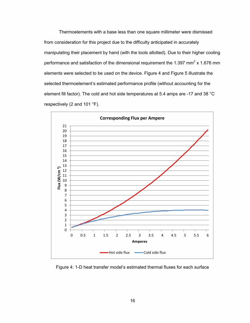
Thermoelements with a base less than one square millimeter were dismissed
from consideration for this project due to the difficulty anticipated in accurately
manipulating their placement by hand (with the tools allotted). Due to their higher cooling
performance and satisfaction of the dimensional requirement the 1.397 mm2 x 1.676 mm
elements were selected to be used on the device. Figure 4 and Figure 5 illustrate the
selected thermoelement’s estimated performance profile (without accounting for the
element fill factor). The cold and hot side temperatures at 5.4 amps are -17 and 38 °C
respectively (2 and 101 °F).
Figure 4: 1-D heat transfer model’s estimated thermal fluxes for each surface
0 1 2 3 4 5 6 7 8 9
10 11 12 13 14 15 16 17 18 19 20 21
0 0.5 1 1.5 2 2.5 3 3.5 4 4.5 5 5.5 6
Flu
x (W
/cm
2)
Amperes
Corresponding Flux per Ampere
Hot side flux Cold side flux

17
Figure 5: 1-D heat transfer model’s estimated temperatures for each surface
Modeling Conclusions
Of the thermoelements accessible to the lab, the 1.397 x 1.397 x 1.676 mm
thermoelement size was chosen for this design because of its peak cooling performance
at 5.4 A; 4.0352 W/cm2 cooling flux, and cold and hot side temperatures of -17 and 38
°C. These thermoelements would have a column oriented arrangement and alternate
between p and n-type composition (Figure 6). To simplify the design process the base
dimensions of the thermoelement are rounded up to 2 mm, allowing the approach of
referencing the device’s dimensions in terms of equivalent thermoelements. The Circuit
Boards section explains how this was implemented. The results were overlay
dimensions of 2.44 x 3.23 inches (62 x 82 mm). This is just beyond the 2 x 3 inch (50.8 x
76.2 mm) approximated requirement but is worth the compromise (see Adjusted
Performance Estimates) with 180 thermoelements. It was also concluded that the best
way to safely handle the peak 5.4 A value was if the bottom substrate remained an
uncompromised electrically insulating surface with no holes or separations.
-20
-10
0
10
20
30
40
50
0 0.5 1 1.5 2 2.5 3 3.5 4 4.5 5 5.5 6
Tem
pe
ratu
re (
°C)
Amperes
Corresponding Temperature per Ampere
Hot side temp Cold side temp

18
Figure 6: Example of a side view of a column based arrangement of thermoelements mounted perpendicularly to electrically conductive material
Forearm Modeling
It is necessary to quantify the body’s combating heat flux. In this chapter a lower
bound estimate of the forearm’s heat flux was calculated as the sum of convection,
radiation, irradiation, and evaporation fluxes from the skin’s surface. Furthermore, the
assumption was made that the temperatures experienced by the wearer would not
provoke bodily temperature compensation, including additional perspiration or shivering.
This value was later incorporated in the Adjusted Performance Estimates section to
establish the relativity of the device’s estimated performance.
Lower bound estimates of the forearm heat flux were made using equations from
the model developed by Fiala et al. Their data is based on a humanoid with 73.5 kg of
mass and 14% body fat, in an environment with an effective air velocity of 0.05 m/s
( ), and 30 °C (86 °F) ambient air ( ) and surrounding surface temperatures
( ), where use of in W 2/(K5/2 m4), in W 2s/(m5 K2), and in W 2/(m4 K2) in
Equation 23 are regressed coefficients provided by Fiala et al. [14]
For this research the ambient air and interface temperature were replaced with
21 °C and 29 °C respectively (Environmental Parameters section), and the effective air
velocity was 0.01 m/s. All temperatures used in this section were converted to Kelvin.
The skin’s heat flux, , is the sum of the heat fluxes that interact with the skin’s
surface.

19
Equation 21
where , , , and are the heat fluxes due to convection, radiation, irradiation, and
evaporation, respectively. The irradiation heat flux value was assumed to be zero. The
convection equation is:
Equation 22
where is the temperature of the skin’s surface at the area of interest and is the
temperature of the air. The convection coefficient, in W/(m2 K), is:
Equation 23
The heat flux due to convection was calculated to be 33 W/m2.
The radiation contribution is:
Equation 24
where is the mean temperature of the surrounding surfaces and is the local
radiation heat-exchange coefficient in W/(m2 K), calculated using:
Equation 25
where is the Stefan-Bolzmann constant in W/m2 K4, and are the emissivities
(dimensionless) of the body and surrounding surfaces respectively, and is the
view factor (dimensionless). These values were also provided in Fiala’s paper. [14] The
heat flux due to radiation was calculated to be 37 W/m2.
Assuming steady state and that no water vapor pressure existed on the skin’s
surface the evaporation heat flux calculation is:
Equation 26

20
where is the saturated vapor pressure within the considered area of skin in Pa,
and is the skin moisture permeability W/(m2 Pa). [14] The resulting evaporation flux
is 12 W/m2.
This results in a total forearm heat flux of 82 mW/cm2. When incorporating the fill
factor this results in the TE channel outputting a flux that is more than 80 times greater
than that of the forearm (please see Adjusted Performance Estimates section).
Component Attachment
Even though components attachment is an assembly process it has a great
effect on the circuit’s design. It dictates whether current will be present on two sides of
the board and the properties of solder that should be used. Therefore, these options are
discussed briefly in this section. There are two primary methods for mounting an
electrically conductive circuit board component, either with through hole or surface
mounting techniques. [15]
Through hole mounting requires the circuit board itself to have a hole, or series of
holes, and the attaching component must have an equivalent number of pins. These
holes are located somewhere along the board’s conductive tracing (Figure 7). The pins
of the attaching components pass through the circuit board’s holes and are soldered to
the side opposite where the part took entry (Figure 8). This provides excellent part
attachment because the pins physically anchor the component to the board.
Surface mounting allows for part attachment to a single side of the circuit board
by use of a solder pad. The electrically conductive parts of the component are placed on
top of the solder pad(s) and after reflowing the solder the junction becomes a hardened
joint (Figure 9 and Figure 10). For the reason that surface mounting does not produce
current carrying protrusions on the opposite side of the board and therefore removes a

21
potential source of electric shock to the user, it was chosen as the method of
attachment.
Figure 7: Diagram of intended through hole pin placement to circuit board placement and mating surfaces
Figure 8: Example of a through hole mounted electrical component soldered to a circuit board on the side opposite its insertion
In order to reach the device’s full estimated potential, the circuit board’s traces
must safely operate with current magnitudes up to 5.4 A (see Modeling Conclusions for
details). The thermoelement’s dimensions (1.397 mm2 x 1.676 mm) play a governing
role in determining the solder pad thickness. If the solder pad is too thick then solder
runoff during the reflow process could create thermal and electrical shorts, or bypass the
thermoelement altogether. Furthermore, coating the sides of the thermoelement with
excess solder could cause it to diffuse into the thermoelement during the reflow process,
Solder joints
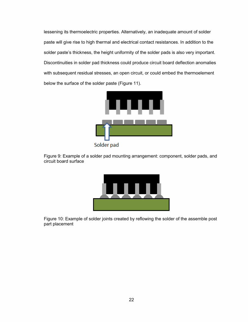
22
lessening its thermoelectric properties. Alternatively, an inadequate amount of solder
paste will give rise to high thermal and electrical contact resistances. In addition to the
solder paste’s thickness, the height uniformity of the solder pads is also very important.
Discontinuities in solder pad thickness could produce circuit board deflection anomalies
with subsequent residual stresses, an open circuit, or could embed the thermoelement
below the surface of the solder paste (Figure 11).
Figure 9: Example of a solder pad mounting arrangement: component, solder pads, and circuit board surface
Figure 10: Example of solder joints created by reflowing the solder of the assemble post part placement

23
Figure 11: Problems resulting from uneven solder pads
Temperature Sensors
A minimum of 6 mm of spacing between circuit channels was selected for two
reasons. This would provide space to accommodate the attachment of one temperature
sensor (measuring approximately 2 mm wide by 8 mm long) within close proximity of
each electrical channel, and still permit adequate flexibility. According to All Flex’s
design guide, “[the] bend radius of a flex should be approximately 10 times the material
thickness.” [16] With 5 channels ( ) there will be 4 locations between them for
temperature sensors ( -1). If those spaces have 4 mm of flexible surface (channel
width, , less sensor width, ) then this contributes to an achievable bending
radius of 16 mm (0.63 in), or a 32 mm (1.26 in) diameter (Equation 27). This is smaller
than the 50.8 mm (2 inch) requirements and according to the All Flex suggestion it
necessitates a substrate thickness of 1.6 mm which is a significantly greater thickness
than what would be utilized for this project. Preferable sensor placement would be at the
center, against the edge of the channel where the cumulative effects of the system’s
heat transfer would be most noticeable.
Equation 27

24
The materials that comprise the circuit board (polymer, adhesive, conducting
element, etc.) must remain functionally stable when exposed to 200 °C (392 °F) for
durations lasting up to an hour. This constraint arises from the conditions of the solder
reflow process.
The device has to be able to accommodate a variety of methods for regulating
the temperature on its outward facing side. Therefore, the surfaces that comprise the
outward face of the device must have independent neutral axes (to allow flexibility),
smooth surfaces (minimize contact resistance), non-permeable (allow for thermal
grease), and rigid (to prevent an additional degree of freedom).
Lastly, the device must allow for the attachment or accommodation of a method
for fastening it to the wearer’s arm. However, a confirmed fastening method was not
configured or established in this research.
Materials
In this section details are provided about the material properties of the circuit
components; thermoelements, substrate material, and solder paste. It also explains the
reason behind their choice.
Thermoelectric Elements
As mentioned previously (Chapter One: Introduction) bismuth telluride performs
well within the temperature range that humans are acclimated to. [10] Table 3 details the
performance of p-type bismuth telluride. These values depend not only on environmental
conditions (temperature, atmosphere, etc.) but on the element’s height (distance
between current carrying surfaces) due to unique interactions with the element’s minority
carriers. [8] Table 4 explains the inputs used in the preliminary 1-D model. Marlow
Industries donated the thermoelements used in this research.

25
Table 4: P-type bismuth telluride properties
Property Value
Seebeck coefficient [8][10]
Thermal conductivity [8]
Electrical resistivity [10]
Table 5: Bismuth telluride properties used in the preliminary 1-D model
Property Value
Seebeck coefficient
Thermal conductivity
Electrical resistivity
Substrate Material
The original intent of this research was to deliver the circuit board’s design to an
outside manufacturer, and upon receipt of the completed circuit board assemble the
device in the lab. However, the feedback received after contacting multiple
manufacturers led to the consensus that this project would have to encompass
manufacturing as well. A possible reason the manufacturers avoided this project is due
to the pre-existing patent on such a device (which was not known at the time). [6]
A search began for flexible circuit board material. The idea of connecting multiple
rigid circuit boards by some flexible means was considered. That approach however
would violate the low level complexity requirement of this project (see Modeling
Conclusions section for details) and was consequently abandoned.
The thickest layer of copper available was sought to safely operate the 5.4 A
current flow, and limit the design’s dependence on trace width compensation for
satisfying the electric load. DuPont’s Pyralux flexible circuit board material, product
FR9610 was selected. This is composed of a 6 ounce (0.0084 inch thick) copper foil
bonded to a 0.001 inch thick polyimide substrate (Kapton) with a flame retardant acrylic
26
adhesive. [16][17] It satisfies the material property requirements; rated for temperatures
beyond 200 °C , and the Kapton provides a volume resistivity of 109 MΩcm. [16][18]
Table 6 details the material properties of the flexible circuit board with adhesive values
taken from a competitor’s product for reference purposes.
Table 6: Material properties of the flexible circuit board
Property Value
Copper – Thermal conductance [12]
Copper – Electrical resistivity [19]
Kapton – Thermal conductance[18]
Kapton – Electrical resistivity [16]
*Adhesive – Thermal conductance [20]
*Adhesive – Electrical resistivity [20]
According to All Flex’s Design Guide the required trace width necessary to
accommodate 6 amps on 6 ounce copper is 1.88 mm (0.074 in). [17] This led to the
decision of designing the trace width to be 2 mm (0.079 in). To provide the 5.4 amps 14
gauge (AWG) wire was to be used. [21] Calculating wire gauge with Equation 28 yields
an anticipated exposed wire diameter of 1.69 mm (0.064 inches).
Equation 28
Solder Paste
The choice of solder paste is largely dependent on the methods it will be applied.
[15,22] For this reason the solder paste’s method of delivery will be selected first. Of the
five methods Coombs (author of the Printed Circuits Handbook) explains for dispensing
solder paste (pin transfer, stencil printing, time pressure-pump, Archimedes screw pump,
positive displacement pump) the stencil printing method was selected because it does
not require the use of a specialized pump or automated equipment. [15] It is something

27
that can be fabricated with the lab’s resources and this process is explained in further
detail in several sections of Chapter Three: Manufacturing.
Coombs recommends that for stencil printing applications a solder paste with a
viscosity of 400 – 800 kcps be used. [15] A 25 gram cartridge of Multicore brand solder
paste, product number SN62RA10BAS86, was purchased online from Newark.com. This
is a 63% tin, 36% lead, and 2% silver paste composition by weight with a viscosity of
500 kcps, melting point of 179 °C (354 °F), and can be used as a no clean solder.
[23][22]
Circuit Boards
Two circuit boards are used to make the column based (Figure 6) thermoelement
arrangement. For simplicity, the thermoelement’s perceived base dimensions were
rounded up to 2 mm during the design of the circuit board’s traces. This allowed for the
trace dimensions to be thought of in terms of equivalent thermoelement count.
Therefore, a single thermoelement was the smallest spacing increment from this
perspective and was chosen as the unit of unoccupied space between thermoelements
of the same channel (Figure 12 and Figure 13).
The intended dimension of each trace segment is 2 mm wide and all of them are
6 mm long, with the exception of the 10 mm long segments that connect to the power
supply on the bottom circuit board. For each channel a 2 mm space is provided between
the trace segments, and a 6 mm space is placed between channels (Figure 13). A total
of five temperature sensors (2 x 8 mm) are to be placed in a 3 x 10 mm space next to
the center point of each channel. With the exception of one outer channel each sensor
occupies the space between the channels (Figure 12).This design allowed for the
placement of 180 thermoelements on a 62 x 82 mm area (2.44 x 3.23 inches). Figure 14
shows the location of the thermoelements on the bottom circuit board. The top circuit

28
board will be cut along the longitudinal centerline between channels to allow for device
flexibility (Figure 15).
Figure 12: Bottom TE circuit traces with designated areas for temp sensor placement
Figure 13: Gap, trace segment, and temperature sensor dimensions for the bottom circuit board

29
Figure 14: Dark squares represent the locations of the 180 thermoelement blocks on the 5 channels of the bottom circuit board
Figure 15: Upper TE circuit traces

30
Adjusted Performance Estimates
In the Device Modeling section it was explained that the area opposite the
thermoelement output cold and hot side temperatures of -17 and 38 °C, respectively, at
5.4 A. Moreover, this produced cold and hot side fluxes of 4 and 17 W/m2 respectively.
These fluxes are based on the area of the elements themselves. However, due to the
spacing between thermoelements, the average cooling and heating capabilities per unit
area are lower. A simple conservative model that takes into account the spacing
between elements of the same channel, but not the spacing between channels or
surrounding substrates was created by assuming that the heat is spread uniformly over
the surface. The fill factor, , is the scalar value used to correct the performance values,
and it’s found by dividing the total area occupied by thermoelements on a given channel
( by the area of that channel ( ) (Equation 29). Figure 16 illustrates
how this value is derived from the present circuit board design.
Equation 29
Figure 16: Dimensions used when calculating the fill factor
A thermoelement occupies 1.952 mm2 of space and there are 36 in one channel.
Therefore is equal to 70.26 mm2. is 468 mm2 and applying these
1
2
1. Channel area = (6 x 78) mm
2. Single thermoelement area = (1.397 x 1.397) mm

31
values to Equation 29 yields a fill factor of 0.15 or 15%. The corrected flux values are the
fill factor multiplied by the previous maximum flux value:
Equation 30
Equation 31
where subscripts C and H indicate hot and cold respectively, and indicates flux. For
the bottom circuit board the corrected cold side flux is 0.61 W/cm2 and hot side flux is 2.6
W/cm2. The device’s surplus power per unit area is calculated by dividing the corrected
cold side flux by the previously calculated forearm heat flux (82 mW/cm2). This
calculation estimates the device’s cooling flux to be 74 times greater than the heat flux
provided by the human forearm. This result supports the notion that the device will cool
the wearer. Heating the bottom circuit board is not a concern because the thermoelectric
effect supplements the Joule heating effect which can be manipulated by simply
increasing the current (Equation 5).
Design for Assembly
A principle that has been successfully applied to many disciplines is the concept
of beginning with the end in mind. [24] Even though assembly is the last step before
having a finished product it should be taken into account through all stages of the design
process. [25] Consideration during the design stage has been made in an effort to
ensure uniform assembly independent of the laborer, make handling the device during
its development stages easier, and prevent costly adjustments from having to be made
near the anticipated end of the project.
For this project three guidelines were applied from the Manufacturing Process
Selection Handbook: [26]
Modularize the design.
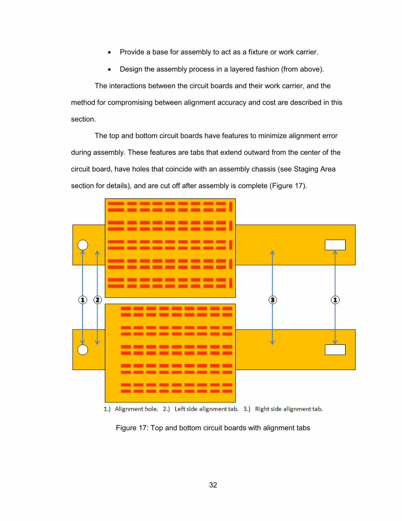
32
Provide a base for assembly to act as a fixture or work carrier.
Design the assembly process in a layered fashion (from above).
The interactions between the circuit boards and their work carrier, and the
method for compromising between alignment accuracy and cost are described in this
section.
The top and bottom circuit boards have features to minimize alignment error
during assembly. These features are tabs that extend outward from the center of the
circuit board, have holes that coincide with an assembly chassis (see Staging Area
section for details), and are cut off after assembly is complete (Figure 17).
Figure 17: Top and bottom circuit boards with alignment tabs

33
The distances from the circuit board to the left and right alignment holes were
computed using the following approach. It was assumed that the alignment holes would
be oversized by a value of :
Equation 32
where is the alignment hole’s equivalent radius and is the radius of the
alignment post, both are in units of meters (Figure 18). The goal was to keep as small
as possible, however, its existence is inevitable in this design scenario. Therefore, the
effects of had to be managed.
Figure 18: Visual representation of Equation 32
Since both circuit boards were aligned to the same posts they would each create
their own angle of misalignment in Rad. This angle gives rise to a misalignment
distance, , expressed by:

34
Equation 33
where is the distance between the staging area’s posts in millimeters and is
calculated as:
Equation 34
where is distance from the left side edge of the circuit board to the center of the left
side alignment hole, is the width of the circuit board, and is the distance from
the right side edge of the circuit board to the center of the right side alignment hole
(Figure 19).
Figure 19: Dimension notation for the preprocessed circuit board
Assuming the center points of the alignment holes for both circuit boards are the
same, then the maximum value of can be expressed as:

35
Equation 35
Combining Equation 33 and Equation 35 offers an approach toward minimizing
alignment error:
Equation 36
Treating as a constant, can be manipulated to achieve a desired ;
where a small or large value produces a large or small , respectively. The sum
of and needed to be as small as possible because the maximum error could be
approximated by the block misalignment at the center point of the circuit board’s right
side edge. This led to an asymmetric design for the circuit board tabs (Figure 20).
Figure 20: Demonstrated benefit of asymmetric preprocessing circuit board design

36
Optimizing Preprocessing Design
Taken as a reference it was assumed that was equal to half the difference
between the major and minor diameter of a 1/4 x 20 stud, 0.79 mm (0.0312 inches). [27]
Table 7 details the values assigned to (left side alignment tab width), , ,
(circuit board height), and (alignment tab height).
Table 7: Preliminary board dimensions used for alignment and cost optimization
Dimension Value (mm)
25.4
12.7
82
62
An undefined cost value was associated with a unit area of circuit board
material. This allowed for assessing cost increases associated with increasing .
Equation 37 calculates the percent alignment improvement ( ) from each incremental
increase of , where is the corresponding displacement error at the edge of
the circuit board. This could be compared to the cost resulting from increasing sacrificial
alignment material. To do this the total alignment material from each increase is
normalized to the fixed area of the circuit board ( , Equation 38). The desired
value is the one that produces the minimum difference between and ;
values were increased by 12.7 mm (0.5 inch) increments, is assumed to be greater
than , the products associated with equal to zero are neglected, and so are the
areas of the alignment holes.
Equation 37

37
Equation 38
The 12.7 mm in Equation 38 is the chosen width beyond the alignment hole that
comprises the right side alignment tab, (Figure 19). This method resulted in a
value of 158.75 mm (rounded to 6.25 from 6.229 inches). However, a calculation
error was observed after the circuit board had been assembled. Correct manipulation of
this approach would have suggested a value of 145.5 mm (5.73 inches)(Figure
21). The alignment holes in the left and right alignment tabs are 6.4 and 6.4 x 12.7 mm
respectively (0.25 and 0.25 x .5 inches).
Figure 21: Alignment improvement and normalized tab area both as functions of

38
Staging Area
The staging area had to meet the following requirements (required material
properties based off of values catalogued at room temperature):
Provide a base for assembly to act as a fixture or work carrier. [25]
Design the assembly process in a layered fashion (from above). [25]
Be able to withstand repeated exposure to temperatures reaching 300 °C
(572 °F) for lengths up to one hour.
Not adhere to polyimide when exposed to high temperatures.
Be able to have solder flux cleaned from it.
Have a thermal conductivity greater than 15 W/(m K).
Possess a thermal expansion coefficient less than 100 m2/s.
Be made from cost effective material.
Ideally weigh less than 5 lbs.
The Circuit Boards section provided details about the preprocessing board’s
dimensions, most notably the 158.8 mm (6.25 inch) space between the center points of
6.4 mm (0.25 inch) diameter posts. The material chosen was aluminum and its material
properties are listed in Table 8. Soldering aluminum requires a different flux and solder
material than what is being used in this research. [28] Also there have been no instances
in the lab where the polyimide has adhered to the aluminum during their mated exposure
to temperatures greater than 200 °C. Lastly, while aluminum’s relative cost is about 8
times higher than steel’s, it’s lower density is more favorable (steel: 8000 kg/m3), and it’s
not as costly as magnesium (15 times greater than steel). [19]
Table 8: Material properties of 2046-T6 aluminum alloy
Property Value
Melting temperature [12] 502 °C
Thermal conductivity [12] 177

39
Table 8 (Continued)
Coefficient of thermal expansion [19] Density [12] 2770
The base plate for the staging area was made rectangular, 101.6 x 203.2 mm (4
x 8 inches) and 6.4 mm (0.25 inches) thick, to facilitate easy manufacturing with
accessible stock. The alignment posts have a 6.4 mm diameter and are 31.8 mm (1.25
inches) long. They were pressed into holes 22.2 mm away from the 101.6 mm edges
along the centerline between the 203.2 mm edges (Figure 22). The machine shop at the
University of South Florida donated the aluminum necessary for the staging area and
assembled it as well (Figure 23).
Figure 22: Staging area assembly view from multiple perspectives and dimensioned

40
Figure 23: Full scale staging area manufactured by the University of South Florida machine shop

41
CHAPTER THREE: MANUFACTURING
Device and assembly components not available by a third party supplier are to
be made using standard manufacturing practices. Due to tooling costs this project
utilized less automation than what could be seen in industry. However, all of the
methods applied can be adapted for mass production. The manufacturing processes
applied were milling operations and chemical etching. Their respective procedures and
results are cataloged in this chapter.
Manufacturing Process Overview
There are three unique types of items that have to be made for this project; the
circuit boards, solder stencil, and thermoelement templates. The key steps in each are
briefly summarized below and then described in more detail.
Each of the circuit boards are cut from stock material, given a rough polish on the
copper side, covered with a patterned etchant mask, submerged in an etchant, removed
from the etchant and chemically neutralized after the unwanted copper has dissolved,
removed of their etchant mask, and given a final rough polish prior to assembly.
The goal of the solder stencil is to apply a uniform layer of solder on each circuit
board that is close to 10% of the thermoelement’s height (a value of 0.168 mm). It is
made by cutting the stencil using a 3-axis mill, cleaning out debris, and deburring by
hand.
The thermoelement templates are used to aid in correct placement of the 180
thermoelements, and to prevent placing a p and n-type element in the wrong location.

42
Each template is cut using a CNC mill (Techno Inc., Model: Davinci Series 1012) to
create the desired apertures and cleaned before use.
Procedures
Etching Procedure
The following step by step description of the finalized etching process used for
creating the circuit boards was developed from multiple sources and personal
experience. [29–32] The etching trials followed a very similar procedure with minor
variations such as different ironing techniques and corresponding work area
arrangements, and post abrading cleaning methods.
The etching process involves the use of an etchant (corrodes the surface of the
work piece) and an etchant mask (a layer that is chemically neutral to the etchant). Once
the work piece materials are identified, in this instance copper and brass, an etchant
specific to the material must be selected. Ferric chloride was the etchant used in this
research and while it reacts with all metals it is typically used to etch copper. The etchant
mask utilized was primarily laser printer toner and acrylic paint was used for touching up
areas of poor transfer.
A drawing of the desired pattern is printed in black ink on common overhead
projector transparency using a laser printer. The surface of the work piece receiving the
etchant mask was first abraded longitudinally and laterally with Grade 3 (coarse) Rhodes
American steel wool. That process was then repeated with Grade 0000 (fine) Rhodes
American steel wool. After that a paper towel was used to remove the surface debris. In
preliminary tests, the surface was rinsed with acetone and then wiped with a paper towel
but that step was removed because its contribution toward developing an oxide layer on
the work piece’s surface had not been quantified.

43
The work piece was placed on top of a folded cotton shirt. This would aid in
uniformly distributing pressure and restrain work piece movement with frictional
resistance during the ink transfer process. Next, the patterned transparency was aligned
with the work piece and fixed to the work table at one end by two clamps.
A household Shark GI468 iron was set to its polyester setting and swept along
the full length of the transparency, from the clamped side downward, with the pressure
you might apply when sealing an envelope. A transparency with 7 inches of swept length
was covered in approximately 4 seconds with each pass. This was done for 2 minutes
and then the iron was rested (hot side down) on top of the transparency for 30 seconds.
The process concluded with sweeping the iron across the transparency for 1 minute. For
cool down the work piece was left in place for 2 minutes, and then the transparency and
work piece with bond intact were transferred to a room temperature surface. After a
minimum of 6 minutes have passed the transparency was peeled from the work piece.
Figure 24: Mock example of ironing arrangement for ink transference to brass or copper. Above, Top view. Bottom, Isometric view

44
This process was derived through multiple trial and error attempts where heat
setting, ironing method, and duration were varied. It was also found that; the iron is
hottest at the frontal tip, the printer ink can be moved under shearing forces along the
surface of the transparency at temperatures of 85 °C or higher, and that the ink does not
coalesce as a droplet at 130 °C (testing was not conducted beyond that temperature).
The middle observation enforces the need for a sweeping motion to take place for
successful transfer of the toner from the transparency to the metal. Areas of poor
transfer are touched up by hand with acrylic paint and allowed to dry overnight.
The part is then submerged in etchant until only the desired material remains.
The etching duration is dependent on the size of the etched surface area, the material’s
desired etched depth, the temperature of the solution, if the etchant is circulated in some
fashion, and the condition of the etchant prior to etching.
In the finalized etching process the etchant bath was contained in a 2 L plastic
container, heated to 50 °C, and agitated with air blown beneath the surface of the
solution. A magnetic stirrer was previously used but in between etching inspections it
proved to be difficult to reposition the stirrer underneath a protective cage that kept it
from colliding with the material.
After etching was completed the part was removed from the solution and
chemically neutralized with baking soda. The resulting solids were wiped from the part
and it was washed with soap and water. The remaining etchant mask was cleaned off by
spraying the component with acetone and wiping it clean.
Milling Procedure
The object to be milled attached to an intermediary plastic board with masking
tape. This board serves as a sacrificial surface during the milling process in order to
prevent the mill bit from damaging the mill table. This board has also been sanded down
on all surfaces between uses to prevent significant surface burrs (due to previous milling

45
operations) from disturbing the mating of the material to the board, and the board to the
mill table.
The board is then placed up against a 90° frame on the mill table. The board is
fully restrained by 3 tapered work piece restraints. Depending on the work piece, WD-40
may be sprayed on the surface as a cooling film during metal to metal contact (the
toughest material milled are 0.014 inch thick brass sheets).
The motor and desired bit are attached to the mill head. An engraving bit was
used with an offset center where the edge angles were 15° and 30°. The plunge and
movement speeds were set to 5 inches per minute, and the motor operated at 25,000
rpm. When lubricant is used the partitioning mill head brush is also attached to contain
the spatter.
After the safety shield is lowered the mill is turned on and controlled from the
computer with the Techno GCODE Interface Program (Appendix D: Stencil and Middle
Template Gcode). From here inputs can be entered manually through the Jog graphical
user interface or by uploading a predesigned program (written in Gcode). The finished
product is removed from the mill table and cleaned of debris and liquid. Next the work
piece is removed from the intermediary board and further cleaned.
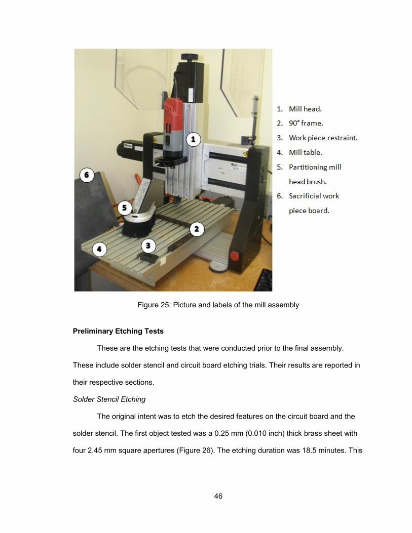
46
Figure 25: Picture and labels of the mill assembly
Preliminary Etching Tests
These are the etching tests that were conducted prior to the final assembly.
These include solder stencil and circuit board etching trials. Their results are reported in
their respective sections.
Solder Stencil Etching
The original intent was to etch the desired features on the circuit board and the
solder stencil. The first object tested was a 0.25 mm (0.010 inch) thick brass sheet with
four 2.45 mm square apertures (Figure 26). The etching duration was 18.5 minutes. This

47
value is fast comparatively speaking but it’s because the part was simultaneously etched
on both sides.
The result was a mean aperture square side length of 2.37 mm with a standard
deviation of 0.074 mm, and a deposited solder paste thickness of approximately 0.41
mm (Figure 27). Exact reasons for the deposited solder paste being thicker than the
stencil are unknown; it is believed to be a function of the smearing method, and
parallelism between the entirety of the circuit board and solder stencil surfaces.
Figure 26: First etched sample – Brass trial solder stencil
Figure 27: Deposited solder using the first brass stencil
A solder stencil was made for the first trial assembly (Figure 28 and Figure 29).
The apertures were designed to be 2 mm squares. However, the mean length of the

48
square aperture was 2.27 mm (0.0894 inches) with a standard deviation of 0.198 mm
(0.0078 inches).
Figure 28: Negative image for the transparency of the second etched solder stencil
Figure 29: Second etched brass solder stencil
Circuit Board Etching
The negatives of the first trial circuit board were created (Figure 30). Following
the successful completion of all the steps leading to post etching cleanup it was
observed that circuit board’s traces were smaller than designed. This was the result of
the etchant corroding the copper at the perimeter of the mask as the surrounding
surfaces deteriorated. This unanticipated corrosion removed approximately 1 mm from
the width and height of each trace (Figure 31). The pitting and rough surfaces that
developed from this process might have been a consequence of either inadequate touch
up work or from leaving the part in the etchant for too long. In the first several etching

49
attempts permanent marker was used to touch up the work pieces. However, by the third
trial assembly this was abandoned entirely and only acrylic paint was used. Subsequent
masks oversized the traces by 1 mm in each direction to compensate.
Figure 30: Negative image for the transparency of the first trial assembly
Figure 31: Etched results for the first trial assembly
The negatives for the second trial circuit board were oversized from the first
attempt (Figure 32). However the top circuit board was patterned twice. To correct this
the extended trace width for the power connections were painted on. The etching
duration was approximately 1 hour and 20 minutes. The circuit boards resulting from the
post etching clean up can be seen in Figure 33. The reduction in surface pitting
(compared to Figure 31) is the result of an improved etching mask transference and
touch up procedure. Although it was not realized until after the two boards were
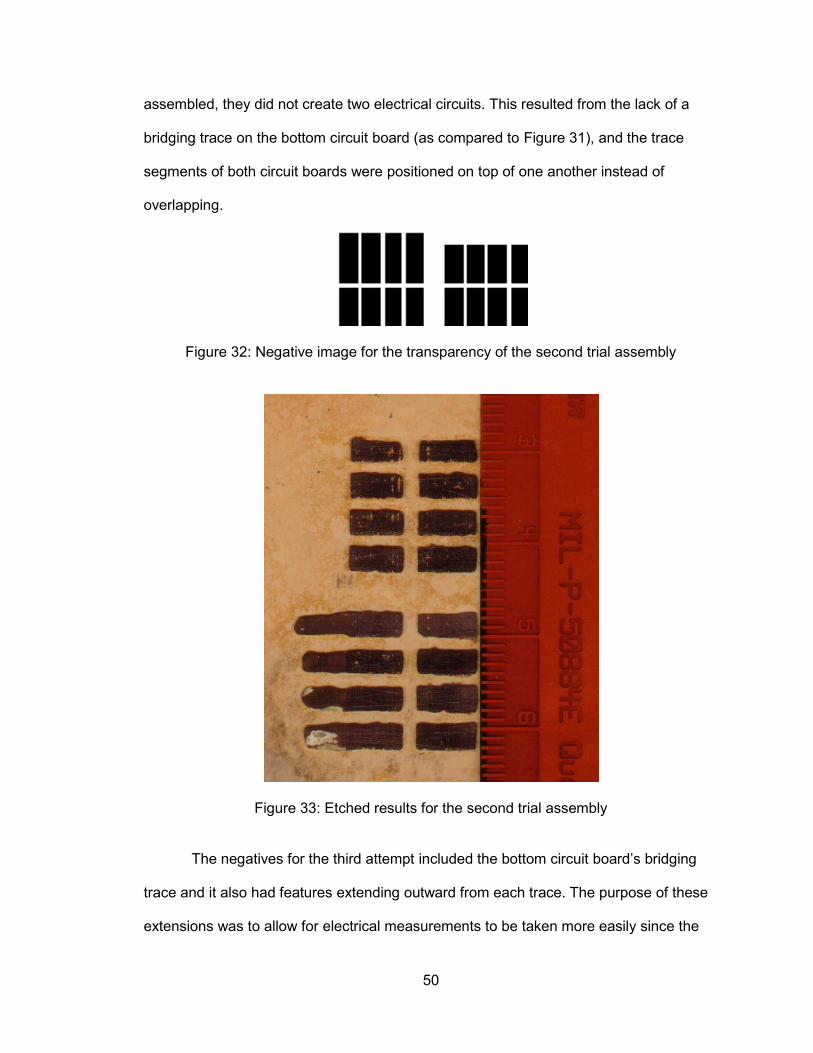
50
assembled, they did not create two electrical circuits. This resulted from the lack of a
bridging trace on the bottom circuit board (as compared to Figure 31), and the trace
segments of both circuit boards were positioned on top of one another instead of
overlapping.
Figure 32: Negative image for the transparency of the second trial assembly
Figure 33: Etched results for the second trial assembly
The negatives for the third attempt included the bottom circuit board’s bridging
trace and it also had features extending outward from each trace. The purpose of these
extensions was to allow for electrical measurements to be taken more easily since the
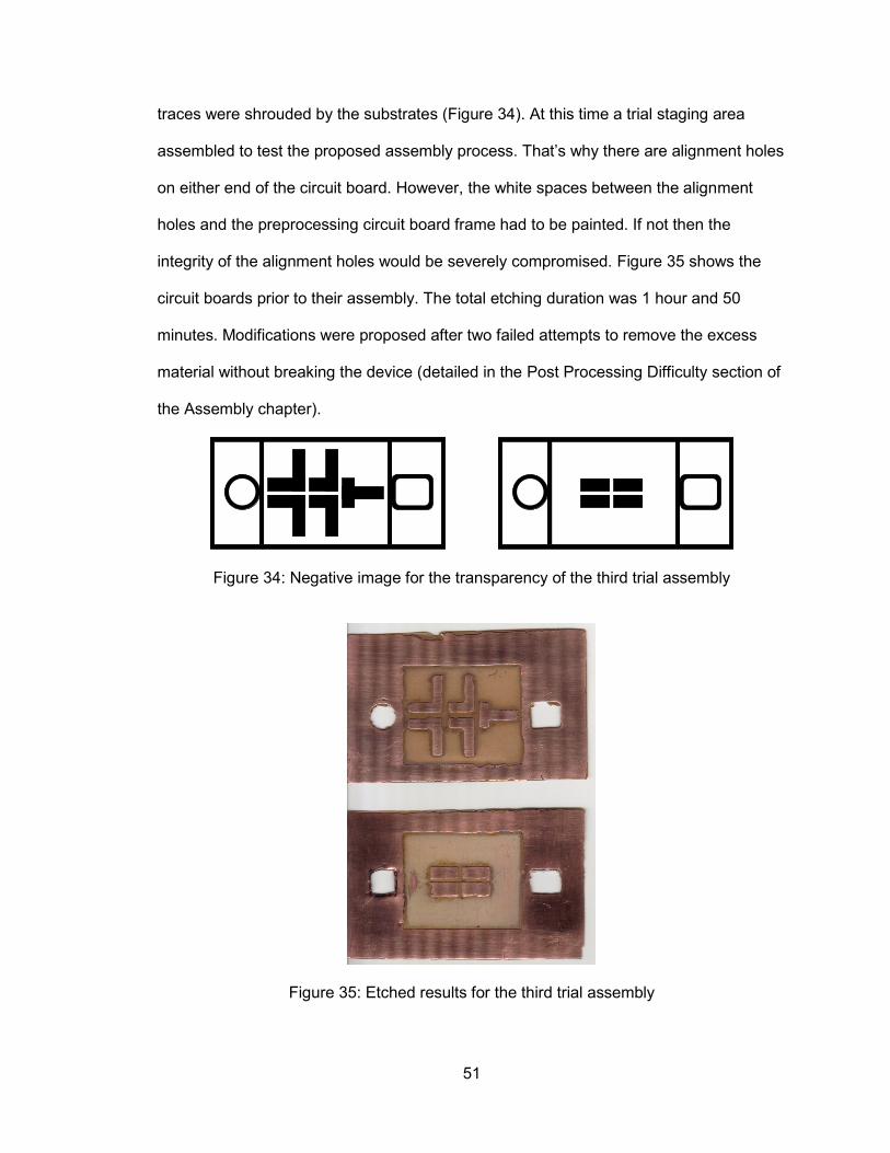
51
traces were shrouded by the substrates (Figure 34). At this time a trial staging area
assembled to test the proposed assembly process. That’s why there are alignment holes
on either end of the circuit board. However, the white spaces between the alignment
holes and the preprocessing circuit board frame had to be painted. If not then the
integrity of the alignment holes would be severely compromised. Figure 35 shows the
circuit boards prior to their assembly. The total etching duration was 1 hour and 50
minutes. Modifications were proposed after two failed attempts to remove the excess
material without breaking the device (detailed in the Post Processing Difficulty section of
the Assembly chapter).
Figure 34: Negative image for the transparency of the third trial assembly
Figure 35: Etched results for the third trial assembly
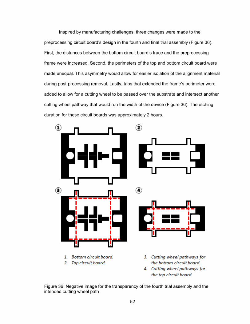
52
Inspired by manufacturing challenges, three changes were made to the
preprocessing circuit board’s design in the fourth and final trial assembly (Figure 36).
First, the distances between the bottom circuit board’s trace and the preprocessing
frame were increased. Second, the perimeters of the top and bottom circuit board were
made unequal. This asymmetry would allow for easier isolation of the alignment material
during post-processing removal. Lastly, tabs that extended the frame’s perimeter were
added to allow for a cutting wheel to be passed over the substrate and intersect another
cutting wheel pathway that would run the width of the device (Figure 36). The etching
duration for these circuit boards was approximately 2 hours.
Figure 36: Negative image for the transparency of the fourth trial assembly and the intended cutting wheel path

53
Preliminary Milling Tests
These are the milling tests that were conducted prior to the final assembly. These
include solder stencil and thermoelement template milling trials, where 1 mm and 2 mm
aperture sizes were analyzed as well. Their results are reported in their respective
sections.
Solder Stencil Milling
The possibility of milling the solder stencil was explored after seeing the results
obtained from etching 0.25 mm (0.010 inch) thick brass sheets. A thinner material was
also chosen; copper foil with a thickness of 0.10 mm (0.004 inch) replaced the brass.
With this foil a comparison was made between the solder deposited from 2 mm and
1mm aperture sizes (Figure 37). Also included in this comparison were the results from
reflowing the solder at different temperatures.
Figure 37: 2mm and 1mm aperture milled solder stencils
It was observed that heating the solder paste until the oven air temperature
reached 180 °C produced inadequate solder joints. As illustrated in Figure 38, the solder

54
grains barely melted if at all. From this figure it is also interesting to note that the solder
paste thickness deposited by the copper foil is four grains or less.
Figure 38: 1mm and 2 mm apertures, solder reflow at 180 °C
It was not until the oven air temperature reached 190 °C that a satisfactory solder
joint was produced. However, two short comings are observable for each aperture size.
Figure 39 illustrates the potential for developing significant air gaps if thermoelement
alignment is not controlled with exacting precision. Air gaps like these create poor
thermal conductivity at the thermoelement to circuit board interface, and limit the amount
of electrical current that can safely pass through that junction. Ultimately the factors
result in poor thermoelectric performance.
The glossy translucent film on the left image of Figure 40 might represent the
solidification of solder flux byproduct around the base of the thermoelement. This
creates an alternative thermal pathway around the thermoelement and diminishes

55
device performance. Be that as it may this problem can be addressed by cleaning the
solder joints with the appropriate solution and agitation method.
Figure 39: Two samples of the 1 mm aperture, solder reflow at 190 °C
Figure 40: Two samples of the 2 mm aperture solder reflow at 190 °C
The results from using the 1 mm aperture and 200 °C oven air temperature
illustrate the ideal mating between the thermoelement and the circuit board (Figure 41).

56
Conversely, use of the 2 mm aperture at the same temperature shows signs that the
solder paste is gathering where the excess flux was previously (judging by the dull
tapering surface at the base, Figure 42).
Figure 41: Two samples of the 1 mm aperture solder reflow at 200 °C
Figure 42: Two samples of the 2 mm aperture solder reflow at 200 °C

57
Figure 43: Top view of solder reflow results from different temperature exposures and stencil (1mm and 2mm) uses
Figure 44 demonstrates the solder joint quality of the first trial assembly. The 2
mm square dimension aperture was made in the 0.10 mm (0.001 inch) thick copper foil.
The thermoelement on the left hand side of the figure has solder paste ascending the
thermoelement’s faces. While the right hand side thermoelement has only minor
soldering imperfections on the thermoelement. Due to the alignment forgiveness
inherent to using a larger solder pad and to continue working with the 2 mm
thermoelement convention the 2 mm apertures were selected for continued use.

58
Figure 44: Profile picture taken of the first trial assembly to analyze solder joint quality
However, it was found that the brass foil underwent plastic deformation too easily
during its own manufacturing and when used as a stencil. In an attempt to overcome this
problem the stencil was mounted to a wooden rectangular frame in much the same way
a painter’s canvas would be (Figure 45); the frame was built first, the copper foil was
wrapped around it, and the apertures were made last. However, there was about 6.35
mm (0.25 inches) of deflection at its center. Moreover, the need to ensure the frame’s
planar uniformity added another potential source of assembly error. Inconsistencies in
this planar face would contribute to a non-uniformity of solder paste thickness.
Multiple aperture sets were made in the framed solder stencil at different
locations to allow for analysis of the hole’s dimensional dependence on its proximity to
the wooden frame. This was not completed however because an alternative solder
stencil material was being investigated; due to the fragile nature of the copper foil and
the added complexity of incorporating a frame.

59
Figure 45: Framed 2 mm solder stencil
The transparency film was tried as a solder stencil material (Figure 46). It was
also 0.10 mm (0.004 inch) thick and all deformations that took place while being
manipulated were within the material’s elastic region. Additional benefits were realized
when comparing this to copper; less aggressive on the mill’s bit, no need for liquid
cooling, and no perforation crown on the side opposite where the mill bit takes entry.
There is however the risk of developing micro frays along the aperture’s perimeter if not
milled properly.
Figure 46: Transparency based solder stencil used on third and fourth trial assemblies

60
Thermoelement Template Milling
The thermoelement templates were made from 0.36 x 101.6 x 254 mm (0.014 x 4
x 10 inch) brass sheet stock, where three 38.1 x 101.6 mm (1.5 x 4 inch) sections were
cut off for the templates. Since they were cut with shears there was curling that occurred
across the width of the segment. This required them to be hammered flat, however the
surface’s unevenness was still apparent.
They were milled (with inputs provided manually) independently (Figure 47). The
top template provides a fixed alignment space for placing p-type thermoelements. The
middle template is similarly used to provide a fixed alignment space for placing the n-
type thermoelements on the remaining solder pad vacancies. The bottom template acts
as a shim that prevents the middle template from disturbing the circuit board’s solder
paste.
Figure 47: Brass thermoelement alignment templates for the third and fourth trial assemblies. (top) Elevates the middle template above the solder’s height. (middle) Used for the remaining vacancies (n-type thermoelements) (bottom). Used for p-type thermoelement placement.

61
Staging Area
The trial assembly staging area (Figure 48) is made from a plate of what is
believed to be plain carbon steel. The hole at the top serves no purpose for this project,
this steel was previously kept in the lab for miscellaneous use. The intended distance
between the center points of the alignment posts was 41.27 mm (1.625 inches).
Threaded studs (1/4 x 20 x 3) were used in place of pressed in posts. The holes for
these studs were drilled with a 0.125 inch pilot hole and again with a #7 drill bit. Then
they were tapped for 1/4 x 20 thread.
Figure 48: Trial assembly stage with a stainless steel base and two 1/4 x 20 x 3 studs.
Final Component Results
This section explains the manufacturing results obtained producing the circuit
boards, solder stencil, and thermoelements templates. It also explains the unique
developments that influenced their final manufacturing method.
Circuit Boards
Due to the unanticipated erosion on the periphery of each trace segment the
mask’s trace segment dimensions were: 3 x 7 mm, 3 x 11 mm on the power connection
segments, a 1 mm space between segments of the same channel, and 5 mm of space
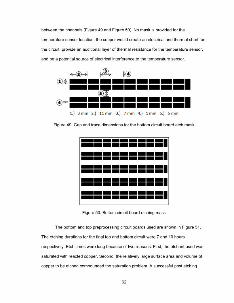
62
between the channels (Figure 49 and Figure 50). No mask is provided for the
temperature sensor location; the copper would create an electrical and thermal short for
the circuit, provide an additional layer of thermal resistance for the temperature sensor,
and be a potential source of electrical interference to the temperature sensor.
Figure 49: Gap and trace dimensions for the bottom circuit board etch mask
Figure 50: Bottom circuit board etching mask
The bottom and top preprocessing circuit boards used are shown in Figure 51.
The etching durations for the final top and bottom circuit were 7 and 10 hours
respectively. Etch times were long because of two reasons. First, the etchant used was
saturated with reacted copper. Second, the relatively large surface area and volume of
copper to be etched compounded the saturation problem. A successful post etching

63
bottom circuit board was not achieved until the third attempt. The first attempt’s possible
causes for failure were from collision with the magnetic stirrer and an inadequate
duration for allowing the touch up paint to dry (2 hours). The second attempt failed
because the preliminary circuit board frame did not surround the board’s entire
perimeter, and a small incision compromised this area. Subsequently this led to the
polyimide tearing under its own weight during routine etching inspection.
Figure 51: Post etching bottom (1) and top (2) circuit boards for the full scale assembly

64
Solder Stencil
The idea of creating the solder stencil apertures by etching was abandoned in
favor of the CNC mill. Even though etching offered the ability to create multiple parts in a
single batch of solution there was also a longer preparation time required (transferring
the mask) and a time dependency on etching performance (etching process slows as it
becomes saturated with dissolved material).
To avoid the possibility of ruining a work piece by human error the mill was
operated by a pre-written program rather than manual individual inputs at the time of
manufacturing. A MATLAB program was written to create the g-code for the stencil
design (see Appendix C: MATLAB Gcode Generator for code details). Figure 52
illustrates the programmed pathway for the cutting tool.
Figure 52: Automated pathway preview of the mill’s cutting tool for the full scale transparency based solder stencil
The four standalone holes in the final solder stencil (Figure 53) were from the first
automated attempt of the solder stencil. Due to the plunge depth set at that time the
apertures were made too wide, shortening the space between them. This was corrected
by milling under sized apertures and boring them out afterward with a separate milling
operation (work piece was not removed and reference positions remained the same).

65
The choice to bore the holes out instead of increasing the plunge depth during the initial
pass is because the increased plunge depth will result in shortening the spaces between
the apertures, a vital distance to maintain for the solder stencil.
Figure 53: Transparency based solder stencil for the full scale assembly
Thermoelement Templates
Like the full scale transparency solder stencil the thermoelement templates were
created using the milling process, where the inputs were automated by programs written
for each template (see Appendix D: Stencil and Middle Template Gcode for sample
code). Figure 54, Figure 55, and Figure 56 illustrate the programmed pathways the
cutting tool would take for the bottom, middle, and top templates respectively. The same
0.36 x 101.6 x 254 mm (0.014 x 4 x 10 inch) brass sheets that were used for the trial
templates were used for the full scale templates. Since the sheets were longer than
desired their lengths were cut down to 203 mm (8 inches) with a Dremel cutting disk.
This tool was used to remove the excess material without bending the sheet. These
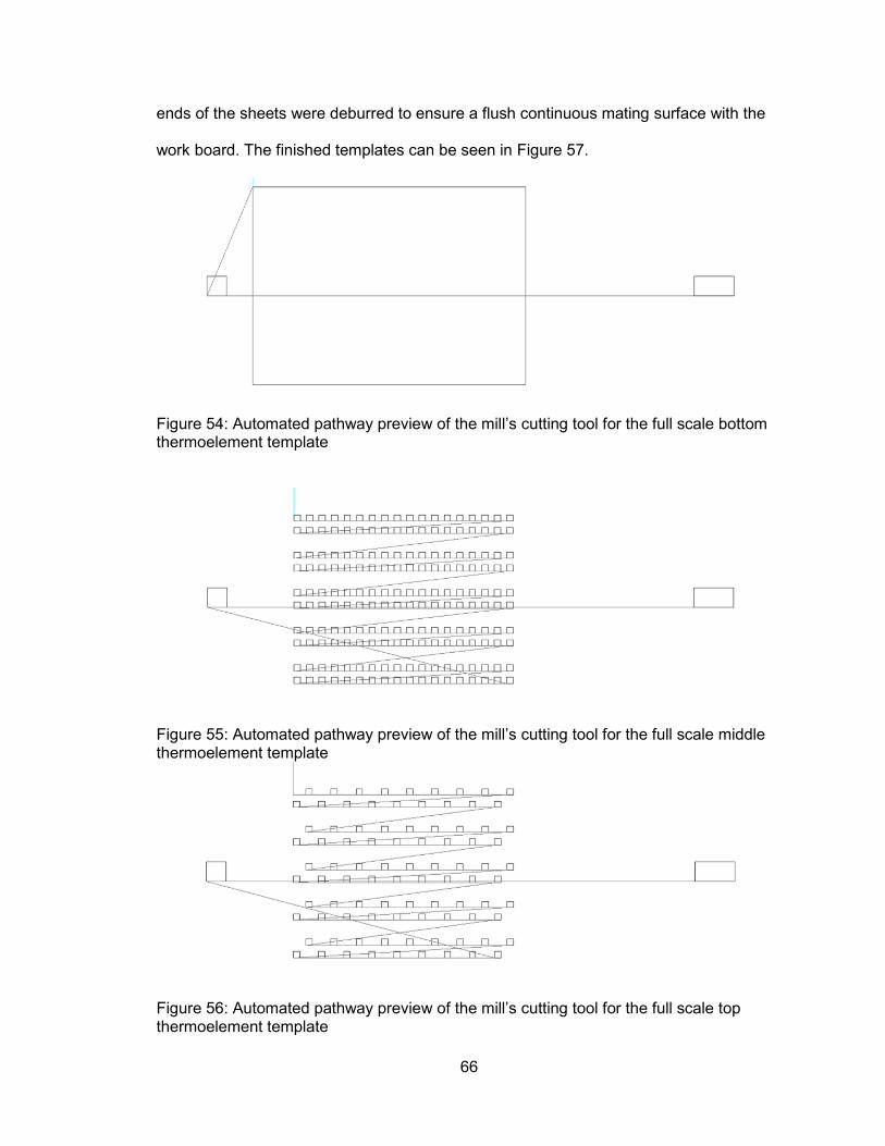
66
ends of the sheets were deburred to ensure a flush continuous mating surface with the
work board. The finished templates can be seen in Figure 57.
Figure 54: Automated pathway preview of the mill’s cutting tool for the full scale bottom thermoelement template
Figure 55: Automated pathway preview of the mill’s cutting tool for the full scale middle thermoelement template
Figure 56: Automated pathway preview of the mill’s cutting tool for the full scale top thermoelement template

67
Figure 57: Finished full scale thermoelement templates. 1.) Bottom full scale thermoelement template. 2.) Middle full scale thermoelement template. 3.) Top full scale thermoelement template

68
CHAPTER FOUR: ASSEMBLY
The following chapter explains how all of the components come together in a
step by step process. The development of this final procedure was not arrived upon
immediately. Some of the problems encountered had their origins in manufacturing or
even design, and had to be addressed accordingly.
Steps
The steps taken to assemble the trial devices are the same as those used for the
full scale device. For this reason there will often be pairs of figures representing each
step. One picture will be a schematic of the process and the other will be the result of
carrying out that process on the final device.
First the top circuit board is placed on the staging area and the solder stencil is
placed on top of the circuit board (Figure 58 and Figure 59). Solder paste is then
deposited by hand with the syringe the paste came in. The syringe is held a quarter inch
above the circuit board and an excess amount is deposited in each of the stencil’s
apertures (about two to three times the aperture’s volume). From previous trials it was
found that it’s better to have an excess amount of solder in the aperture ready for wiping
than just what appears to fill the space. Once all of the apertures are adequately filled a
brass sheet is used to wipe the solder paste across the stencil (Figure 58). The
deposited solder paste was then examined to see how well it filled the aperture. If there
were any gaps a small amount of paste was deposited at the specific aperture and the
stencil was wiped over again at that location.

69
The solder stencil and top circuit board are then removed. The bottom circuit
board is then placed on the staging area and this process is repeated, with the exception
that the circuit board is not removed at the end. This creates discrete solder pads on
each circuit board (Figure 60, Figure 61, and Figure 62).
Figure 58: Schematic of solder paste application process

70
Figure 59: Solder stencil on top of the top circuit board prior to solder paste application
Figure 60: Schematic of the post solder paste application results
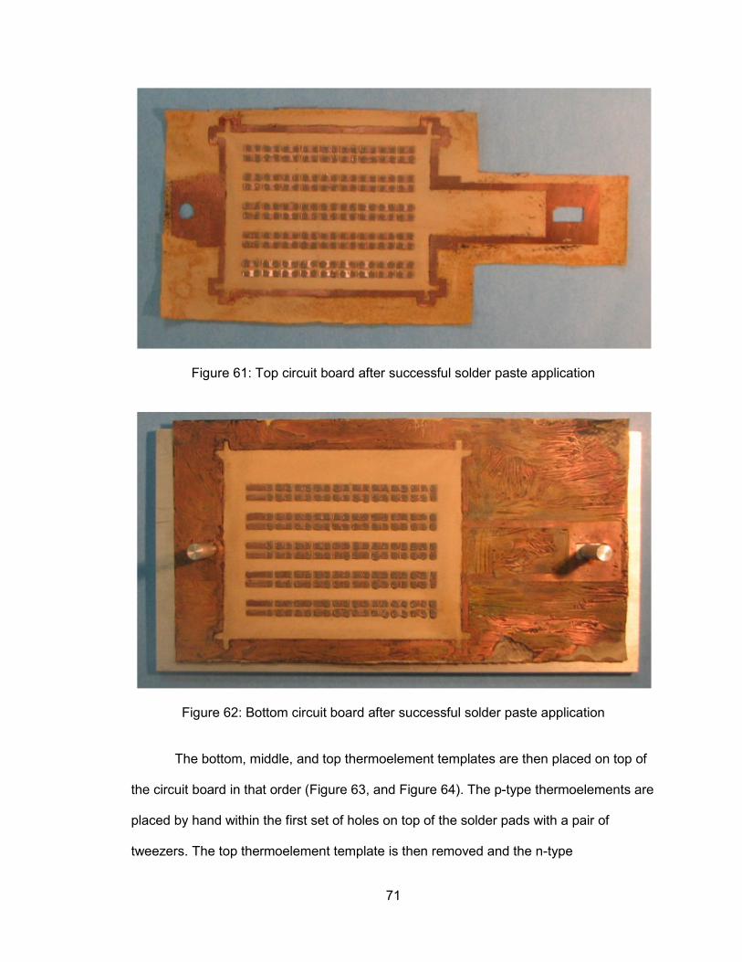
71
Figure 61: Top circuit board after successful solder paste application
Figure 62: Bottom circuit board after successful solder paste application
The bottom, middle, and top thermoelement templates are then placed on top of
the circuit board in that order (Figure 63, and Figure 64). The p-type thermoelements are
placed by hand within the first set of holes on top of the solder pads with a pair of
tweezers. The top thermoelement template is then removed and the n-type

72
thermoelements are placed in the remaining middle template vacancies in the same
manner (directly corresponds to vacant solder pads)(Figure 65). The middle and bottom
thermoelement templates are removed, leaving the bottom circuit board populated with
thermoelements (Figure 63, Figure 66, and Figure 67).
The top circuit board is then placed on top of the staging area’s arrangement
(Figure 68). A mass is added to apply pressure and the assembly is then placed in the
oven (Figure 69). For the trial assembly this mass was 92 g and for the full scale
assembly it was 292 g. Both had the bulk of this mass focused at the center but for the
full scale assembly the resulting pressure was almost evenly distributed across the
assembly by the thermoelement templates (Figure 69). This assembly was then placed
in the oven (Thelco, Model 27). The time and temperature profile for reflowing the solder
is dependent on the size of the circuit board assembly (for further detail refer to the Final
Assembly Results and Discussion section of this chapter).
The arrangement is removed from the oven once the appropriate time has
passed and it has cooled down to room temperature. The assembly is then removed
from the staging area. In the finishing process, the thermoelectric device is cut from the
surrounding alignment material. This is done by stacking three 0.36 mm (0.014 inch)
brass sheets and placing them in between the surfaces of the circuit board. A cutting
wheel is rolled along the inside rigid edge of the top circuit board (refer to Figure 36 in
the Circuit Board Etching section of the Manufacturing chapter) and the brass sheets act
as a table keeping the circuit board level during this process. This is repeated along the
perimeters of each circuit board. The end result is the extracted thermoelectric device
(Figure 70 and Figure 71).
In the full scale and final trial scale assembly wires were soldered to the device
after verifying electrical continuity. Acetone was applied to the power supply connections
on the device and were brushed clean. Any remaining residue was wiped off prior to

73
soldering. Next 26 AWG wire was soldered to each power supply connection from the
device with thin gauge solder (brand unknown), rosin soldering flux (RadioShack part
number 64-022), and a 45 watt pencil iron (Craftsman model number 954042) (Figure
71).
Figure 63: Schematic of the thermoelement and thermoelement template application process

74
Figure 64: Bottom, middle, and top thermoelement templates applied to the bottom circuit board

75
Figure 65: Top thermoelement template removed after p-type thermoelements are positioned
Figure 66: Remaining thermoelement templates removed after n-type thermoelements are positioned
Figure 67: Close up of the thermoelements positioned on the bottom circuit board
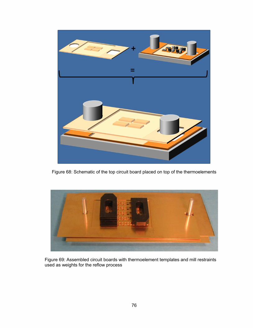
76
Figure 68: Schematic of the top circuit board placed on top of the thermoelements
Figure 69: Assembled circuit boards with thermoelement templates and mill restraints used as weights for the reflow process
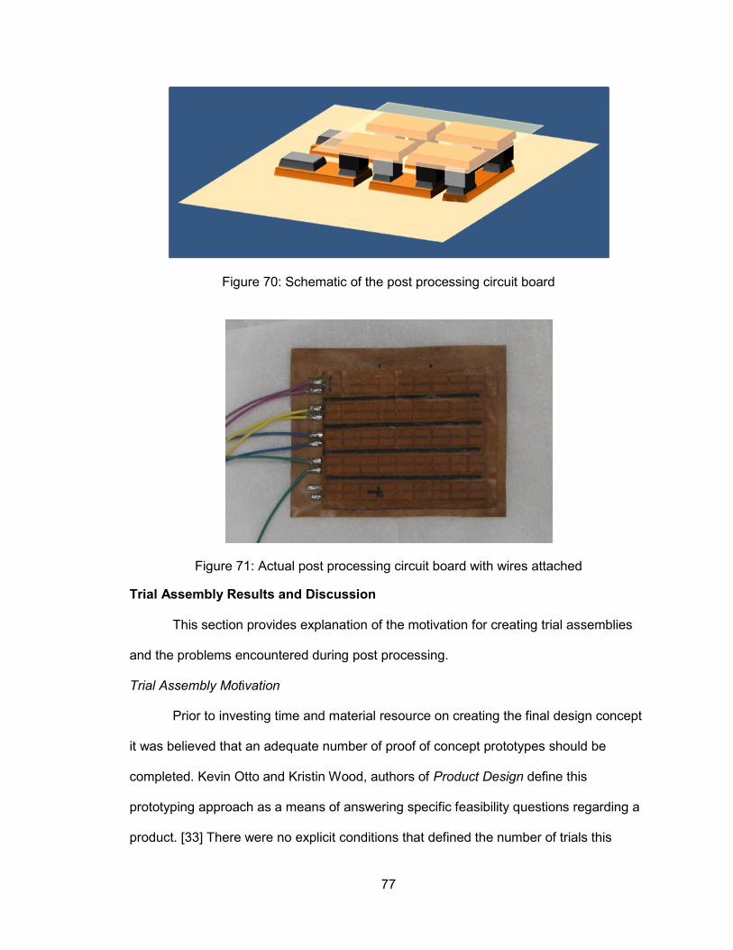
77
Figure 70: Schematic of the post processing circuit board
Figure 71: Actual post processing circuit board with wires attached
Trial Assembly Results and Discussion
This section provides explanation of the motivation for creating trial assemblies
and the problems encountered during post processing.
Trial Assembly Motivation
Prior to investing time and material resource on creating the final design concept
it was believed that an adequate number of proof of concept prototypes should be
completed. Kevin Otto and Kristin Wood, authors of Product Design define this
prototyping approach as a means of answering specific feasibility questions regarding a
product. [33] There were no explicit conditions that defined the number of trials this

78
project would create, only that there were enough to justify the validity of the
manufacturing and assembly approaches.
The first two prototypes (Figure 72 and Figure 73) were made with the purpose of
evaluating the manufacturing approaches for the circuit board and solder stencil. They
were assembled without the aid of alignment tools or the staging area. Questions were
asked like “can this produce the desired geometry,” and “does this result appear to be
repeatable?” The discussion on those matters is in the Manufacturing section of the
Conclusions chapter, but the short answer is yes.
Figure 72: Top view of the first trial assembly
Figure 73: Top view of the second trial assembly

79
The first trial assembly (Figure 72) showed the need for increasing the individual
trace segment dimensions of the etching mask to compensate for the erosion that
occurred around the trace segment periphery during etching. This approach was applied
in subsequent etching procedures because it improved the accuracy of the trace
segment dimensions produced. The second trial assembly (Figure 73) is the result of an
improved etching mask transference, touch up procedure, and the first application of the
etching mask’s dimensional compensation for the etching process. The incision which
separated the top substrate between the two intended channels also allowed for
demonstration of the design’s flexibility.
The next two prototypes (Figure 74 and Figure 75) were made to demonstrate
the soundness of the assembly process and utilized the manufacturing lessons learned
from the previous two prototypes. These assemblies incorporated the trial staging area,
methods for aligning the components, and use of thermoelement templates. Again, the
questions that dictated the project’s direction were with regards to accuracy and
repeatability of the process (see Manufacturing Conclusions).
Figure 74: Top view of the third trial assembly

80
Figure 75: Top view of the fourth (final) trial assembly
The third trial assembly (Figure 74) proved the repeatability of this assembly
approach by the ease in which the multiple repairs were made to the device. The final
trial assembly demonstrated the achievement of a working thermoelectric device by this
assembly method. From this it was concluded that adequate manufacturing and
assembly methods had been developed in order to begin production of the full scale
device. A transparent superposition of the fourth assembly on top of the third assembly
reveals the manufacturing and assembly processes repeatability (Figure 76).
Figure 76: Transparent superposition of the fourth trial assembly on top of the third trial assembly

81
Post Processing Difficulty
The first attempt at removing the excess material was during the third trial
assembly. The alignment tabs of both circuit boards were cut simultaneously with
scissors. This resulted in the planar rotation of the top circuit board relative to the bottom
one, shearing the solder joints. After being repaired another attempt was made. In an
effort to change the plane of motion, and remove the moment arm that previously
contributed to failure, one of the alignment tabs were bent upwards at 90° prior to being
cut with industrial shears. However, this again resulted in failure. A Dremel cutting disk
ultimately separated the device from the alignment material. Despite the success of this
approach an alternative method that did not involve the use of a power tool was
preferred. This motivated the design changes for the fourth trial assembly iteration and
the use of a cutting wheel. This worked successfully on the full scale and final trial
assemblies.
Final Assembly Results and Discussion
Difficulty was encountered in properly reflowing the solder on the full scale
assembly. The oven’s air temperature was measured by a thermal probe inserted at its
exhaust vent at the top of the oven. This sensor penetrated several inches into the
oven’s atmosphere but never touched the device. During the first reflow attempt the
oven air heated to 200 °C with the oven turned off at that point, as was done during the
trial assemblies (Table 9). However the door remained closed for 11 minutes 21 seconds
(instead of the 1 minute used during trial assemblies), at which time the air temperature
reached 170 °C. This was done as a cautious attempt to provide additional heat
exposure to the larger assembly. After visual inspection of the solder joints it was
concluded that the solder was not adequately reflowed. The joints looked like those in
Figure 38 from the Solder Stencil Milling section of the Manufacturing chapter.

82
Table 9: Time and temperature profile for the first full scale solder reflow attempt
A 10% increase in the temperature set point for turning off the oven (220 °C), and
keeping the oven door closed until the inside air reached the solder paste’s melting point
(179 °C) was decided. Table 10 shows the temperature profile of the second reflow
attempt. The resulting joint quality is comparable to that seen in Figure 44.
Table 10: Time and temperature profile for the second full scale solder reflow attempt

83
Figure 77: Comparison between temperature profiles of the solder reflow attempts
Closing Remarks
There was measured continuity in all of the circuit’s channels following the
completion of the device. In the days following, the bottom channel of the device
developed an intermediate open circuit. The source of the circuit’s problem was isolated
to the connection of a single thermoelement. An unsuccessful attempt was made to
repair this connection. On the other hand, there may have been electrical shorts
between elements as well as those observed in Figure 67. This could substantially
degrade the device performance. This could be reduced by using smaller apertures, or
thinner stencils to reduce the amount of solder deposited. More pressure during the
stencil operation may also reduce leakage of the paste beyond the stencil holes, and
smoother aperture walls would reduce disturbing the solder when the stencil is lifted.
The troubles experienced reflowing the solder is an indication of an area which
needs to be addressed in greater detail. In order for this process to be repeatable and
100
120
140
160
180
200
220
240
27 28 29 30 31 32 33 34 36 37 38 39 40 41 42 43
Tem
pe
ratu
re (
°C)
Time (min)
Comparison between Temperature Profiles of the Solder Reflow Attempts
First attempt Second attempt

84
reliable the connections at the solder joints must be adequate but not excessive, where
the thermoelement is embedded in the solder paste. Future testing could involve
measuring the circuit board or a component’s temperature with a probe directly instead
of measuring the oven’s air temperature.
In addition to the reflow duration the amount of solder paste deposited also
needs to be addressed. I believe a significant contributor toward the paste’s poor
dimensional tolerance is from boring the apertures. Had they been cut as well as the trial
stencil’s I don’t believe problems related to excessive solder paste would be so
prevalent.

85
CHAPTER FIVE: DEVICE PERFORMANCE
The goal of the following chapter is to provide an explanation on how the
interpreted pilot performance data was achieved. This will involve explaining the device’s
testing and data collection methods, the results of this data, and how it compares with
the 1-D model.
Testing Methods
The following section details the data acquisition system, and testing
arrangement for the thermoelectric device. The average time it took to test each channel
was 15 minutes. The average change in surface temperature for the hot and cold side
reservoirs over the course of each test were 2 and 6 °C, respectively. The elevated hot
side temperatures were a significant reason for the relatively large change in the cooling
reservoir’s temperature
Data Acquisition
The data was obtained by using 5 resistance temperature detectors (RTDs).
Each RTD was attached to a Wheatstone bridge, which housed 3 other resistors (values
ranging from 100 to 200 ), a variable resistor (used to adjust the RTD’s resistance),
and a 0.1 F capacitor on the output voltage signal for conditioning. From there the data
was relayed to an analog to digital converter (ADC) (Phidgets, part number 1018-2). This
digital information was then relayed to a computer by USB. A MATLAB program was
written to interface with the ADC (Appendix G: MATLAB Temperature Sensor
Measurement Code). MATLAB then took the information and applied a conversion
formula that was made during sensor calibration. The result was an on screen display of

86
continuously captured temperature data (in Fahrenheit) whenever the program was
running. Once the program completed its cycle it exported the data into a spreadsheet
for analysis and closed communication with the Phidgets device.
Temperature Sensor Calibration
Each temperature sensor was submerged along with a Type K thermocouple
(provided the measured reference temperature) in water at two different temperatures.
Table 11and Table 12 illustrate the resistance values gathered during sensor calibration.
Table 11: Hot temperature exposure for sensor calibration
RTD Display Value Temperature (°F)
Sensor 0 328 111
Sensor 1 335 109.9
Sensor 2 240 107.1
Sensor 4 300 106.4
Sensor 5 240 105.9
Table 12: Cold temperature exposure for sensor calibration
RTD Display Value Temperature (°F)
Sensor 0 97 55.2
Sensor 1 106 55
Sensor 2 31 54.8
Sensor 4 91 55.2
Sensor 5 40 55.9
These values were used to approximate the equation of a line (Equation 39)
which would allow for converting the resistances into temperatures within MATLAB.
Equation 39
where y is the temperature value converted from the sensor’s resistance, x is the
sensor’s resistance, a is the slope in degrees of temperature per resistance, and b is the
y intercept in degrees of temperature. Table 13 details the values of these constants for
each sensor.
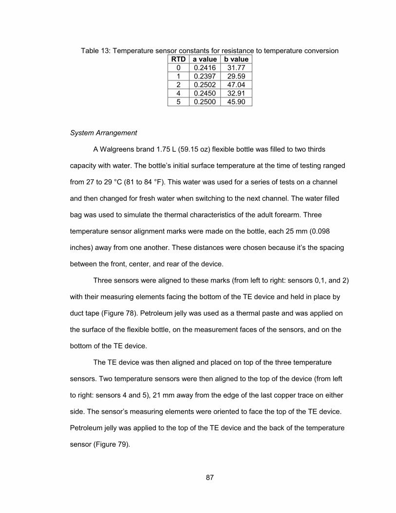
87
Table 13: Temperature sensor constants for resistance to temperature conversion
RTD a value b value
0 0.2416 31.77
1 0.2397 29.59
2 0.2502 47.04
4 0.2450 32.91
5 0.2500 45.90
System Arrangement
A Walgreens brand 1.75 L (59.15 oz) flexible bottle was filled to two thirds
capacity with water. The bottle’s initial surface temperature at the time of testing ranged
from 27 to 29 °C (81 to 84 °F). This water was used for a series of tests on a channel
and then changed for fresh water when switching to the next channel. The water filled
bag was used to simulate the thermal characteristics of the adult forearm. Three
temperature sensor alignment marks were made on the bottle, each 25 mm (0.098
inches) away from one another. These distances were chosen because it’s the spacing
between the front, center, and rear of the device.
Three sensors were aligned to these marks (from left to right: sensors 0,1, and 2)
with their measuring elements facing the bottom of the TE device and held in place by
duct tape (Figure 78). Petroleum jelly was used as a thermal paste and was applied on
the surface of the flexible bottle, on the measurement faces of the sensors, and on the
bottom of the TE device.
The TE device was then aligned and placed on top of the three temperature
sensors. Two temperature sensors were then aligned to the top of the device (from left
to right: sensors 4 and 5), 21 mm away from the edge of the last copper trace on either
side. The sensor’s measuring elements were oriented to face the top of the TE device.
Petroleum jelly was applied to the top of the TE device and the back of the temperature
sensor (Figure 79).

88
Figure 78: Water bottle with bottom sensors attached
Figure 79: TE device with sensors on both its underside and topside

89
The cooling for the top side of the TE device was provided by a 0.562 L (19 oz)
Bard disposable urine bag. This product was used because in future testing it will act as
a flexible fluid reservoir that will allow cooling fluid to flow through it. The initial
temperature of the bag ranged from 21 to 19 °C (70 to 67 °F). Water in the cooling bag
was also replaced when switching to test a new TEC channel.
The cooling bag was positioned, with its center line as close to the center line of
the channel being tested, on top of this assembly while holding the top side
temperatures in place by their wire ends (Figure 80).
Figure 80: Complete TE device testing arrangement
A power source (Electro Industries Model DIGI 185) was used to supply the TE
device with the desired current. Prior to connecting the power source to the device the
amperage value was adjusted while connected to a 1Ω resistor which could handle 50 W
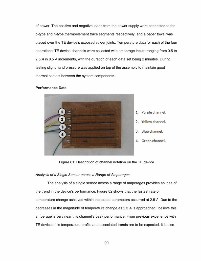
90
of power. The positive and negative leads from the power supply were connected to the
p-type and n-type thermoelement trace segments respectively, and a paper towel was
placed over the TE device’s exposed solder joints. Temperature data for each of the four
operational TE device channels were collected with amperage inputs ranging from 0.5 to
2.5 A in 0.5 A increments, with the duration of each data set being 2 minutes. During
testing slight hand pressure was applied on top of the assembly to maintain good
thermal contact between the system components.
Performance Data
Figure 81: Description of channel notation on the TE device
Analysis of a Single Sensor across a Range of Amperages
The analysis of a single sensor across a range of amperages provides an idea of
the trend in the device’s performance. Figure 82 shows that the fastest rate of
temperature change achieved within the tested parameters occurred at 2.5 A. Due to the
decreases in the magnitude of temperature change as 2.5 A is approached I believe this
amperage is very near this channel’s peak performance. From previous experience with
TE devices this temperature profile and associated trends are to be expected. It is also
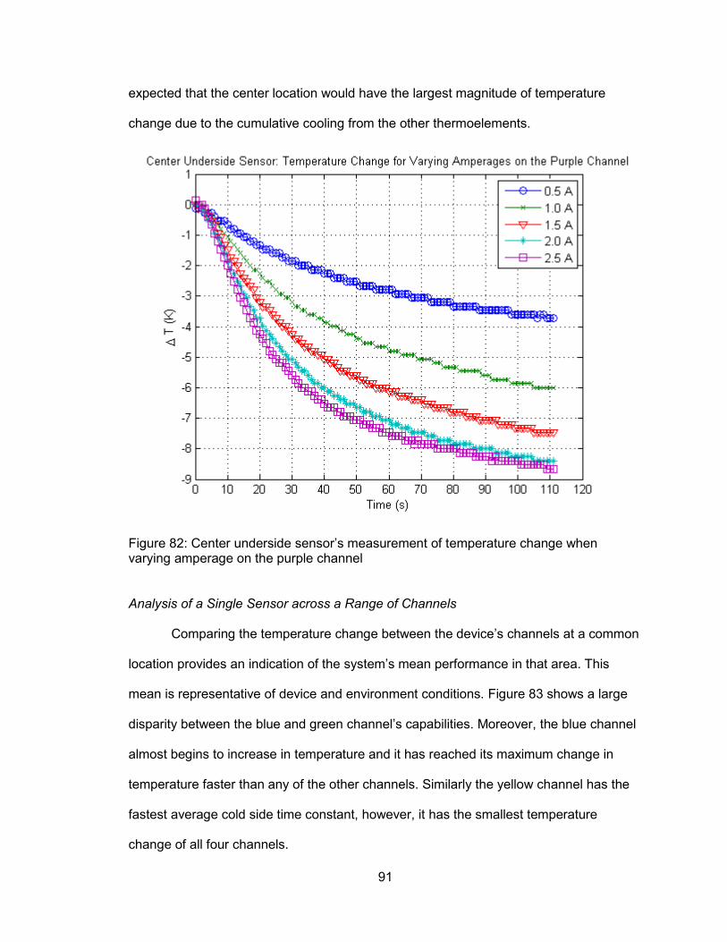
91
expected that the center location would have the largest magnitude of temperature
change due to the cumulative cooling from the other thermoelements.
Figure 82: Center underside sensor’s measurement of temperature change when varying amperage on the purple channel
Analysis of a Single Sensor across a Range of Channels
Comparing the temperature change between the device’s channels at a common
location provides an indication of the system’s mean performance in that area. This
mean is representative of device and environment conditions. Figure 83 shows a large
disparity between the blue and green channel’s capabilities. Moreover, the blue channel
almost begins to increase in temperature and it has reached its maximum change in
temperature faster than any of the other channels. Similarly the yellow channel has the
fastest average cold side time constant, however, it has the smallest temperature
change of all four channels.

92
Figure 83: Left underside sensor’s measurement of temperature change at different channels for 2.5 A
Analysis of a Single Channel at a Constant Amperage
Reviewing the temperature data from multiple locations on a single channel
provides insight on the system as a whole. Figure 84 shows the temperature readings at
five different locations on the TE device. According to the data depicted in the graph
there is a significant temperature gradient occurring on the left hand side of the device.
Also the center underside temperature initially cools down at the same rate as the left
side of the device. However after 20 seconds it begins rising in temperature. It was
found that all but the purple channel would cool at the center and then increase in
temperature, sometimes almost reaching their initial temperature. Reasons for this
behavior are not understood. It is strongly believed to be the result of an assembly
defect such as shorting of elements due to excess solder as noted above.

93
Figure 84: Temperature changes at different locations of the green channel at 2.5 A
Calculated Time Constants
The temperature change time constant for each channel’s performance, specific
to each supply amperage, was calculated for each sensor’s location. This involved
calculating the difference between the initial ( ) and final temperatures ( ) for the data
set of interest. For the unique instance where the center of the device’s underside began
to warm, was taken as the lowest temperature value prior to the heating
phenomenon. The time at which 63% of this temperature difference occurred, according
to Equation 40, was located. This time value represents the time constant () for that
data set.
Equation 40

94
The average of each channel’s time constants across all amperage ranges and
locations were calculated (Table 14). This shows the trend that as amperage is
increased the final temperature values on the underside are approached much faster.
Alternatively, the increasing topside time constant value indicates that their terminal
temperature values were not reached within the data set.
Table 14: Averaged area and amperage specific time constants
Comparison with the 1-D Model
The following subsections compare the experimental results with the initial 1-D
model and an updated 1-D model which better reflects the device’s final design
Results Comparison with the Initial 1-D Model
The 1-D model in its early state estimates the temperature change rather poorly
when compared to the temperature values gathered experimentally from the center of
the purple channel’s underside. This can be seen graphically in Figure 85, and between
numerical comparisons that can be made with Table 15, where a maximum difference in
temperature values is 26.2 K.
Table 15: Numerical comparison between predicted temperatures from the 1-D model and the experimental values obtained from the underside center of the purple channel
Amperage Predicted
Temperature Value (K)
Experimentally Measured Value (K)
Difference in Temperature (K)
0.5 286.3 296.6 10.2
1.0 279.9 294.3 14.4

95
Table 15 (Continued)
1.5 274.3 292.8 18.5
2.0 269.7 292.2 22.5
2.5 265.8 292.0 26.2
Results Comparison with a 1-D Model Reflecting Final Design
The 1-D model comparison in the previous subsection (Results Comparison with
the Initial 1-D Model) still presumes a composed of an extra layer of copper and
solder. If this were updated to the solder, copper, and polyimide layers that better reflect
the hot side’s conductance then changes from 8990 to 2338 W/(m2 K). Table 16
shows the updated numerical differences between estimated and experimental results,
and Figure 85 makes this graphical comparison with the inclusion of experimental
results. The updated model’s maximum difference from the experimental value is half of
the previous model’s difference (12.9 vs 26.2 K). The peak magnitudes of interest (fluxes
and temperatures) for the new model are explained in Table 17. Figure 86 compares the
cooling flux profiles of the initial and updated 1-D models. From Figure 85 and Figure 86
it can be seen that the temperature profile of the updated 1-D model follows a similar
trend to the experimental results. The predicted temperature change varies by more
than a factor of two. This remaining difference is likely due to a combination of thermal
shorts resulting from, manufacturing errors and incorrect parameter inputs for the 1-D
model.
Table 16: Numerical comparison between estimated temperatures from the updated 1-D model and the experimental values obtained from the underside center of the purple channel
Amperage Estimated
Temperature Value (K)
Experimentally Measured Value (K)
Difference in Temperature (K)
0.5 290.3 296.6 6.25
1.0 286.1 294.3 8.17
1.5 282.9 292.8 9.92
2.0 280.6 292.2 11.6
2.5 279.2 292.0 12.9

96
Figure 85: Comparison between actual results, initial theoretical 1-D estimates, and estimates from the updated 1-D model
Figure 86: Cooling flux comparison between the initial 1-D model and the updated 1-D model which better reflects the final design’s materials and dimensions
Table 17: Updated 1-D model’s peak magnitudes
Parameter Value
Cooling flux, 0.417
Cold side temperature, 278.5 K
Hot side conductance, 2338
Cold side conductance, 1320
260
265
270
275
280
285
290
295
300
0 0.5 1 1.5 2 2.5 3
Tem
pe
ratu
re (
K)
Amperage
Center Underside Measured Temperature Compared to Model Estimations
Actual
Intial Model
Updated Model
0
0.1
0.2
0.3
0.4
0.5
0.6
0.7
0 0.5 1 1.5 2 2.5 3 3.5 4 4.5 5 5.5 6
Flu
x (W
/cm
2)
Amperage
Cooling Performance Comparison between 1-D Models
Initial Model
Updated Model

97
Calculated Seebeck Coefficient
Approximating the device’s equivalent Seebeck coefficient will provide insight on
the magnitude of the device’s thermoelectric inefficiency. In order to calculate this value
for each channel hot and cold reservoirs were placed underneath and on top of the
device, respectively. Their initial surface temperatures were 40 °F and 91 °F (4 and 33
°C). The device was left alone to reach equilibrium between the surfaces and the
reservoirs over the span of 20 minutes. The reservoir surface temperatures and channel
voltages were measured. By this time the heating and cooling reservoirs had reached 87
°F and 46 °F (31 and 8 °C). It was assumed that the device’s surfaces were at the same
temperatures as well. These voltages (Table 18) along with the difference in
temperatures between the surfaces were used in combination with Equation 41 to
calculate an effective module Seebeck coefficient, where represents the number of
thermoelements in a channel (36). In addition to this effective Seebeck coefficient Table
18 also displays estimated material Seebeck coefficients. This was completed using the
updated 1-D model with zero current to approximate the temperature across the
thermoelectric element itself without including the effects of the petroleum jelly or
thermal contact resistance (Table 19). This provides a lower bound on the effective
material Seebeck coefficient.
Equation 41
Table 18: Voltages of each channel when the outermost hot and cold side device surfaces are at 31 and 8 °C
Channel Voltage (V)
Eff Module Seebeck Coeff.
(V/K)
Estimated Material
Seebeck Coeff
(V/K)
Purple 0.047 57 137
Yellow 0.049 59 143

98
Table 18 (Continued)
Blue 0.047 57 137
Green 0.050 60 146
The experimentally calculated module values are approximately 25% of ideal
value (240 V/K). This shows that there is substantial thermal resistance in the device
seeing how these were calculated from temperatures measured at the device’s surfaces
and not at the top and bottom of the thermoelement. Performance would be improved
substantially by increasing the hot and cold side thermal conductances.
Meanwhile, the 1-D model temperature estimates predict the effective Seebeck
coefficient to be at least 59% of their optimal value. This serves as a lower bound
estimate for the device and suggests that the performance could have been degraded by
the assembly process. This could be due to solder contacting the edges of the elements.
That would permit atoms from the solder to diffuse into the elements and decrease their
Seebeck coefficients. This could have also been caused by shorts between adjacent
copper pads due to spreading of the solder paste during solder reflow. Device
performance (time constant, max temperature range) will be improved dramatically when
these issues are resolved.
Table 19: Updated 1-D model temperature inputs and corresponding zero amperage thermoelement surface temperatures
Model Parameter Value (K)
Model input: 281
Model input: 305
Model output: 289.6
Model output: 299.1
Testing Procedure Errors
There were multiple sources of testing errors to be considered. The first source
of error is from the temperature sensors. The differences between calibrated and
reference temperatures were used to estimate the errors in the temperature

99
measurements (Table 20). This was completed by placing the temperature sensors in
mutual contact with the same area (in between my index finger and thumb) as a Type K
thermocouple. These differences represent an inaccuracy in measuring the device’s
temperatures and they are on the same scale as the temperature changes that are
produced on the underside of the device. This could explain the asymmetries between
the underside’s left and right temperature readings (sensors 0 and 2), and the topside’s
left and right temperature readings as well (sensors 4 and 5).
Table 20: Difference between temperature sensor’s value and the temperature obtained by the temperature probe used for calibration
Sensor RTD Temperature (°F) Type K T/C (°F) Difference (°F)
0 89.0 95.5 6.5
1 90.7 93.5 2.8
2 88.8 93.4 4.6
4 90.2 95.7 5.5
5 88.9 95.3 6.4
In an effort to understand the time response of the temperature measurement
system each sensor was placed in between my thumb and index finger and the resulting
temperature readings taken over time were recorded (Figure 87). The sensors take
approximately 30 seconds in order to reach a value within adequate range of the
measured surface. This empirical result falls between the manufacturers specified
response time for measuring water flowing at 0.4 m/s and measuring air flowing at 1 m/s.
[34] This means a significant difference between the actual and measured interface
temperature’s change over time may be occurring because the sensor’s delay is close to
that of the device’s time constant. The differences between actual and measured
temperature, and the system’s time response signifies the present system’s inability to
accurately quantify the device’s temperature profile.
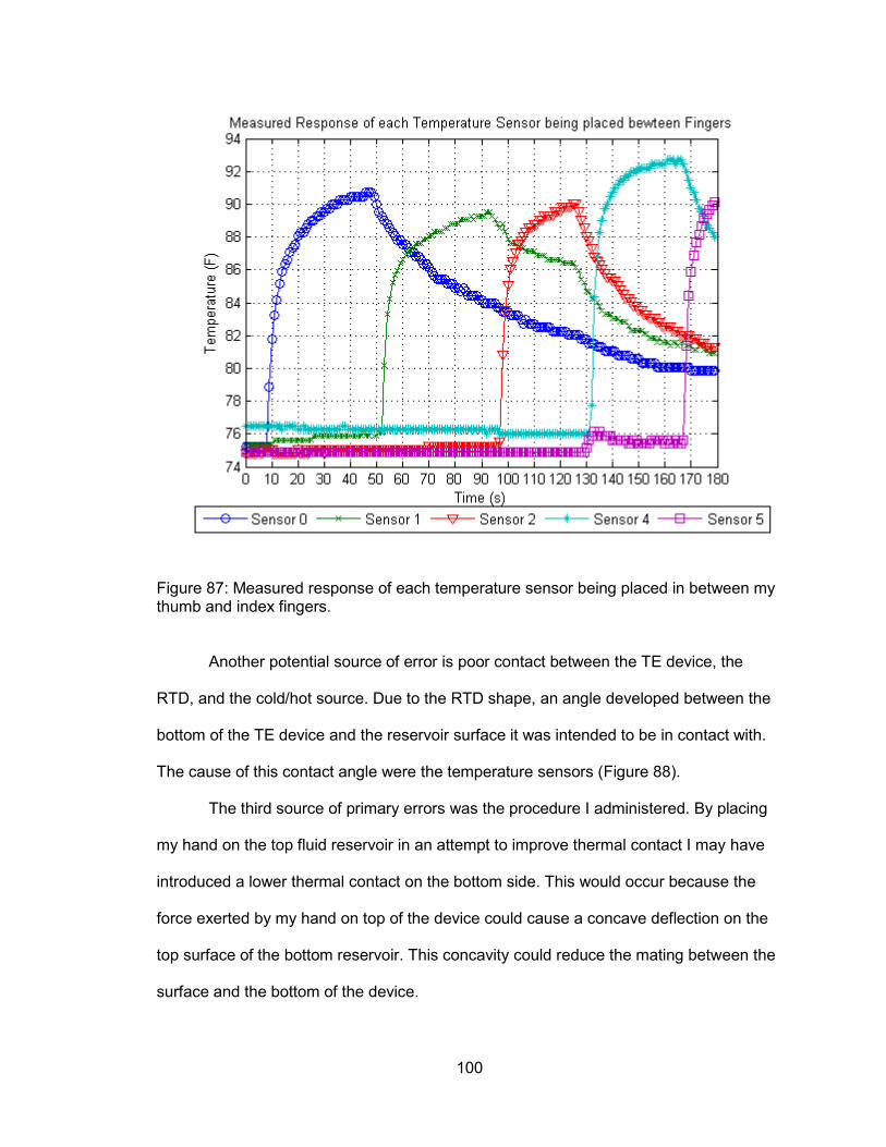
100
Figure 87: Measured response of each temperature sensor being placed in between my thumb and index fingers.
Another potential source of error is poor contact between the TE device, the
RTD, and the cold/hot source. Due to the RTD shape, an angle developed between the
bottom of the TE device and the reservoir surface it was intended to be in contact with.
The cause of this contact angle were the temperature sensors (Figure 88).
The third source of primary errors was the procedure I administered. By placing
my hand on the top fluid reservoir in an attempt to improve thermal contact I may have
introduced a lower thermal contact on the bottom side. This would occur because the
force exerted by my hand on top of the device could cause a concave deflection on the
top surface of the bottom reservoir. This concavity could reduce the mating between the
surface and the bottom of the device.
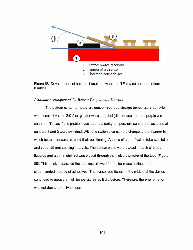
101
Figure 88: Development of a contact angle between the TE device and the bottom reservoir
Alternative Arrangement for Bottom Temperature Sensors
The bottom center temperature sensor recorded strange temperature behavior
when current values 2.0 A or greater were supplied (did not occur on the purple wire
channel). To see if this problem was due to a faulty temperature sensor the locations of
sensors 1 and 2 were switched. With this switch also came a change to the manner in
which bottom sensors retained their positioning. A piece of spare flexible tube was taken
and cut at 25 mm spacing intervals. The sensor wires were placed in each of these
fissures and a thin metal rod was placed through the inside diameter of the tube (Figure
89). This rigidly separated the sensors, allowed for easier repositioning, and
circumvented the use of adhesives. The sensor positioned in the middle of the device
continued to measure high temperatures as it did before. Therefore, the phenomenon
was not due to a faulty sensor.

102
Figure 89: Sensor mounting alternative to tape
Adequacy of Performance
While the device may only create a 2 °C degree interface temperature change in
10 seconds that is still enough for a cold sensation to be recognized (Figure 84).
According to The Fundamentals of Sensory Physiology, a change of -0.2 °C or more
from an adapted temperature of 31 to 27 °C will be recognized as the perception of
something becoming colder. [35] While this requirement has been met, testing has yet to
prove if the device can create an interface temperature as low as 16 °C yet. Assuming
an initial and final interface temperature of 27 and 16 °C, to meet the 8 °C temperature
drop in 10 seconds would require an 8 second time response. Currently the fastest
cooling responses measured are at the center of the device’s underside ( 20
seconds), but an 8 °C temperature decrease is not achieved and heating shortly begins
at that surface after the lowest temperature is reached. Further testing is necessary to
fully understand the scope of the device’s performance. With improved manufacturing
methods, the device performance should improve significantly.

103
CHAPTER SIX: CONCLUSIONS AND FUTURE WORK
This chapter addresses the performance of the test device relative to the project
goals and identifies areas for future work.
Design Conclusions
The seed that gave rise to the results of this research was sown during the
design stage. A one dimensional model was utilized to estimate the performance of
different device configurations. The surface energy balance from the forearm model
allowed for quantifying the adequacy of the proposed design. An understanding of the
device’s parameters and requirements confined and guided the decision making
process. Understanding how the components were going to be attached and keeping the
next step in mind allowed for the device’s development to be fluid and adaptive.
The device has met the reparability requirement. When the wires were first being
soldered to the full scale assembly’s power connections the soldering iron accidentally
unsoldered a thermoelement. However, localized repair was conducted without
damaging the surrounding elements. Occupying a 3 x 4 inch overlay area the overall
device is also within a scale that is comparable to its 2 x 3 inch requirement. The overlay
area is capable of being trimmed down, however, this size was chosen to help distance
body hair and skin from electrically conductive surfaces.
A cost oriented approach toward minimizing alignment was used to reduce
sacrificial material. Lastly an assembly stage was made to establish a datum that would
facilitate the process’ repeatability and ease of handling assembly.
104
Sources of Design Error
The performance of the one dimensional model was a function of the
thermoelectric property data. The lack of material property data (ideally batch specific)
from the manufacturer led to assuming the material matched published values for
bismuth telluride. The errors in these assumptions can have a compounding effect,
especially when the thermal pathway has more than 10 layers (based upon conductivity
and contact resistance).
Likewise, the forearm model provided a lower bound estimate for the skin’s heat
flux since it estimated the outbound heat flux based upon convection, conduction,
evaporation and radiation but neglected conduction. Moreover, it used charted data that
may not be representative of the population this device might interact with.
Future Work for the Design
A possible solution would be to increase the TE model’s complexity to two
dimensions. This will require more familiarity with the subject matter, potentially longer
time spent in the design process, and more terms and assumptions (e.g. initial and
boundary conditions, material, etc.) to be accounted for. These same additions however
are what decrease the model’s sensitivity when compared to the single dimension
alternative.
Manufacturing Conclusions
The overall process was successful in assembling a functional TE device.
However, there were significant defects that must be addressed in order to achieve a
reliable process. Chief among these is the low effective Seebeck coefficient of the
assembled module. This is likely due to excess solder either shorting between elements
or coating elements and degrading their performance. This needs to be addressed by

105
improving the solder application process. Additionally, there was one of the five channels
that had an open circuit rendering it entirely nonfunctional.
There are also opportunities to improve the circuit board patterning process. The
dimensional variation from the various manufacturing processes was not analyzed
rigorously, but attempts were made at quantifying dimensional tolerances. The maximum
observed trace width deviation was approximately 0.002 inch (0.05 mm). Moreover, the
trace widths were all larger than the intended 2 mm. They were 2.4 mm (0.096 inches)
or wider (Figure 90).
Figure 90: Graphical datum analysis used for determining maximum and minimum differences from a specific trace segment within the channel
Sources of Manufacturing Error
There was also an absence of models for the etching and ironing processes. As
a result these were developed by meaningful (an understanding of the contributing
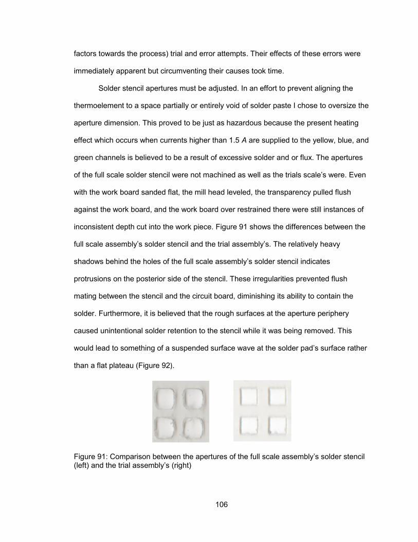
106
factors towards the process) trial and error attempts. Their effects of these errors were
immediately apparent but circumventing their causes took time.
Solder stencil apertures must be adjusted. In an effort to prevent aligning the
thermoelement to a space partially or entirely void of solder paste I chose to oversize the
aperture dimension. This proved to be just as hazardous because the present heating
effect which occurs when currents higher than 1.5 A are supplied to the yellow, blue, and
green channels is believed to be a result of excessive solder and or flux. The apertures
of the full scale solder stencil were not machined as well as the trials scale’s were. Even
with the work board sanded flat, the mill head leveled, the transparency pulled flush
against the work board, and the work board over restrained there were still instances of
inconsistent depth cut into the work piece. Figure 91 shows the differences between the
full scale assembly’s solder stencil and the trial assembly’s. The relatively heavy
shadows behind the holes of the full scale assembly’s solder stencil indicates
protrusions on the posterior side of the stencil. These irregularities prevented flush
mating between the stencil and the circuit board, diminishing its ability to contain the
solder. Furthermore, it is believed that the rough surfaces at the aperture periphery
caused unintentional solder retention to the stencil while it was being removed. This
would lead to something of a suspended surface wave at the solder pad’s surface rather
than a flat plateau (Figure 92).
Figure 91: Comparison between the apertures of the full scale assembly’s solder stencil (left) and the trial assembly’s (right)

107
Figure 92: Intended solder pad profile (left) and an example of the hypothesized solder pad profile (right) produced by the full scale assembly’s solder stencil
Future Work for the Manufacturing Process
It is strongly recommended that an understanding of scientific formulas that allow
for the prediction of outcomes from the ironing and etching process be understood. With
respect to the full scale assembly, the etching process takes the most time to complete.
An understanding of the reaction rates would allow for work load scheduling during the
etching process instead of a guess and check approach which does not provide
schedule consistency.
A reduction in aperture size would decrease the likelihood of solder paste related
inefficiencies: solder diffusion into the thermoelement, alternate thermal pathways
through the thermoelement, and electrical shorting between copper trace segments. A
1.5 mm square aperture size is recommended for future projects with the 1.397 x 1.397
x 1.696 mm thermoelement. This would provide a small tolerance for thermoelement
misalignment with the solder pad. Unlike the 1 mm square solder pad which either has
the thermoelement positioned correctly on top of it or is misaligned. Along with this
should come a minimum standard of machined aperture quality.
Assembly Conclusion
The assembled device allows temperature variance between 4 independent
locations. The fifth channel is inoperable only because of one thermoelement’s
intermittent electrical connection. The device can also be worn and provides enough
flexibility to be draped over an adult’s finger (approximately 0.5 inch bending diameter).

108
Sources of Assembly Error
The circuit boards were not taut when they were placed on top of the staging
area. This ability to gather small cumulative deflections could have been a cause of
unfavorable alignment. Also the lack of an appropriate model for the oven may have led
to diminished device performance due to excessively spreading of the solder during the
reflow process.
Future Work for the Assembly Process
To improve the precision of solder and thermoelement placement a solder stencil
with smaller apertures and corresponding thermoelement alignment templates are
recommended for future builds.
Performance Conclusions
Sources of Performance Error
The dominant source of performance error is in the reduced properties of the TE
elements. This degradation is believed to be due to some combination of solder diffusion
into the TE elements and shorting between copper pads. Both problems are likely
related to excessive solder paste deposition. The effect of this degradation was
quantified by establishing a range of Seebeck coefficient estimates,
(Calculated Seebeck Coefficient).
A flaw was also observed in the previous method of affixing the bottom
temperature sensors; as testing progressed from one channel to the next the device was
moved upward in the direction of the temperature sensors. The sensors acted as a
pivoting point, introducing a ramping effect that produced an angle of separation
between the bottom of the device and the surface of the water bottle. Moreover, the
placement of my hand’s weight on the top of the device may have contributed to
concavities between the temperature sensors and their respective surfaces.

109
The temperature of the reservoirs should also be better controlled. This would
allow for an appropriate comparison between the channels and their respective
performance rather than just proving a trend. It would also presumably permit longer
testing durations, and higher amperages.
Conclusion
All of the suggested corrections for the sources of error were researched to
varying depths. However, the project needed to meet a deadline and this limited further
investigation.
Despite the heat that develops in the middle of the device at amperages above
1.5 A, the device still provides cooling along the bottom surface until that point is
reached. Moreover, the temperature change, albeit small is still within the threshold of
Schmidt’s criteria for sensible temperature change. For this reason and those explained
in Table 21, I believe the research conducted in this project and the resulting design
produced meets the requirements to consider this a successful design, manufacturing,
and assembly project. With some minor process changes, the next iteration in the
process could substantially improve the device performance. If the effective Seebeck
coefficient of the device is raised to even 2/3 of theoretical, then the device should
exceed the design requirements.
The biggest limit to the device performance is the large entry and exit thermal
conductances resulting from the use of a polymer layer. Further improvement could be
achieved by increasing the thermal conductances of these layers.
Table 21: Result comparison between the project requirements and those achieved
Requirement Achieved result
Independently vary temperature at 5 locations.
Independently vary temperature at 4 locations.
Capable of a 2 inch bending diameter. Capable of an approximate 0.75 inch
bending diameter (without temperature sensors attached).

110
Table 21 (Continued)
Wearer is isolated from hazardous components.
Condition satisfied.
Device dimensions of approximately 2 x 3 inches.
Device dimensions of 3 x 4 inches.
Supplies a heat flux greater than 8.2 mW/cm2.
Supplies a heat flux less than 417 W/cm2.
Interface temperature range between 60 and 90 °F.
Maximum interface temperature drop of 18 °F.
Allow temperature sensor attachment. Space allotted for temperature sensor
attachment.
Constructed by standardized manufacturing processes.
Condition satisfied.
Minimal allowable temperature of 56 °F. Device temperature can be regulated to
temperatures above 56 °F.
Not all causes of device failure should be terminal.
Condition satisfied.
Completed by the summer of 2013. Condition satisfied.
111
REFERENCES
[1] Craig A. D., 2002, “How do you feel? Interoception: the sense of the physiological condition of the body,” Nat Rev Neurosci, 3(8), pp. 655–666.
[2] Barrett K. E., and Ganong W. F., 2010, "Ganong’s Review of Medical Physiology," McGraw-Hill Medical, New York, NY. pp. 174.
[3] McClure M., 2012, “Stanford researchers’ cooling glove ‘better than steroids’” [Online]. Available: http://news.stanford.edu/news/2012/august/cooling-glove-research-082912.html. [Accessed: 25-Sep-2012].
[4] Hartemann A., Attal N., Bouhassira D., Dumont I., Gin H., Jeanne S., Said G., and Richard J.-L., 2011, “Painful diabetic neuropathy: Diagnosis and management," Diabetes Metab., 37(5), pp. 377–388.
[5] McKnight P. T., 2010, "Finite element analysis of thermoelectric systems with applications in self assembly and haptics," M.S. thesis, Mechanical Engineering, University of South Florida, Tampa, FL.
[6] Bell L. E., 2004, “Flexible Thermoelectric Circuit,” U.S. Patent 6700052 B2.
[7] Huang I.-Y., Lin J.-C., She K.-D., Li M.-C., Chen J.-H., and Kuo J.-S., 2008, “Development of low-cost micro-thermoelectric coolers utilizing MEMS technology," Sensors Actuators Phys., 148(1), pp. 176–185.
[8] Goldsmid H. J., 2010, "Introduction to thermoelectricity," Springer, Heidelberg; New York. pp. 1-4, 43, 81, 145, 150.
[9] Francioso L., De Pascali C., Farella I., Martucci C., Cretì P., Siciliano P., and Perrone A., 2011, “Flexible thermoelectric generator for ambient assisted living wearable biometric sensors,” J. Power Sources, 196(6), pp. 3239–3243.
[10] Rowe D. M.,2006, "Thermoelectrics handbook: macro to nano," CRC/Taylor & Francis, Boca Raton, FL. pp. 1-3, 1-9, 37-5-7, 9-14.
[11] Ioffe, Abram, 1957, "Semiconductor Thermoelements and Thermoelectric Cooling," Infosearch Ltd., London, England, pp. 44, 85.
[12] Incropera F. P., Dewitt D. P., Bergman T. L., and Lavine A. S., 2007, "Introduction to heat transfer," Wiley, Hoboken, NJ. pp. 61, 102, 103, 126, 840, 843, 850, 851.
[13] Miner A., 2007, “The Compatibility of Thin Films and Nanostructures in Thermoelectric Cooling Systems,” J. Heat Transf., 129(7), p. 805.

112
[14] Fiala D., Lomas K. J., and Stohrer M., “A computer model of human thermoregulation for a wide range of environmental conditions: the passive system,” J. Appl. Physiol. [Online]. Available: http://jap.physiology.org/content/87/5/1957. [Accessed: 20-Jul-2012].
[15] Coombs C. F. 2008, "Printed circuits handbook," McGraw-Hill, New York, New York. pp 40.4-40.29.
[16] DuPont, “DuPont Pyralux FR Copper-Clad Laminates” [Online]. Available: http://www2.dupont.com/Pyralux/en_US/assets/downloads/pdf/FRclad_H-73233.pdf. [Accessed 14-May-2013].
[17] All Flex Flexible Circuits, LLC, “All Flex Design Guide Revised Master Fall 2011.pdf,” Flex Flex. Circuits Heaters [Online]. Available: http://www.allflexinc.com/PDF/All%20Flex%20Design%20Guide%20rev%20Master%20Fall%202011.pdf. [Accessed: 22-Feb-2013]. pp 13, 20.
[18] DuPont, "Summary of properties for Kapton polyimide films," [Online]. Available: http://www2.dupont.com/Kapton/en_US/assets/downloads/pdf/summaryofprop.pdf. [Accessed 14-May-2013].
[19] Callister W. D., 2007, Materials science and engineering: an introduction, John Wiley & Sons, New York, NY. pp. A18, A23, A26, A31-33.
[20] 3M, “3M Scotch-Weld," [Online]. Available: http://multimedia.3m.com/mws/mediawebserver?66666UF6EVsSyXTtnxfcLx46EVtQEVs6EVs6EVs6E666666--. [Accessed 14-May-2013].
[21] Engineering Toolbox [Online], “Amps and Wire Gauge - 12V Circuit,” [Online]. Available: http://www.engineeringtoolbox.com/amps-wire-gauge-d_730.html. [Accessed: 22-Feb-2013].
[22] Loctite, “Product RA10 (Multicore solder cream),” [Online]. Available: http://www.farnell.com/datasheets/314582.pdf. [Accessed 15-May-2013].
[23] “SN62RA10BAS86-25G CARTRIDGE - MULTICORE (SOLDER) - SOLDER PASTE, 62/36/2 SN/PB/AG | Newark,” [Online]. Available: http://www.newark.com/multicore-solder/sn62ra10bas86-25g-cartridge/solder-paste-62-36-2-sn-pb-ag-179/dp/18K6979?in_merch=Popular%20Soldering%20Stations%20And%20Accessories. [Accessed: 15-May-2013].
[24] Covey S. R., 2004, "The 7 habits of highly effective people: restoring the character ethic," Free Press, New York, NY. pp 95.
[25] Boothroyd G., 2005, "Assembly automation and product design," Taylor & Francis, Boca Raton, FL. pp 220.
[26] Swift K. G., 2013, "Manufacturing process selection handbook," Elsevier, Oxford.

113
[27] “ANSI External Screw Threads Size & Tolerances Chart - Engineers Edge” [Online]. Available: http://www.engineersedge.com/screw_threads_chart.htm. [Accessed: 18-May-2013].
[28] Avery W. F., Baskin P. A., "Soldering aluminum," [Online]. Available: http://www.superiorflux.com/papers/Soldering_Aluminum_Brazing_Soldering.pdf, Cleveland, OH. [Accessed 22-May-2013].
[29] Saughnessy L., “Let’s Etch Some Brass! - YouTube,” [Online]. Available: http://www.youtube.com/watch?v=m69aHYMw_yY. [Accessed: 30-May-2013].
[30] Lawton N., “Brass Etching for Beginners,” Etch. Begineers [Online]. Available: http://www.nigellawton009.com/Etching_for_Beginners_Version_5.htm. [Accessed: 30-May-2013].
[31] Gotang, “Etching brass plates,” Etchign Brass Plates [Online]. Available: http://www.instructables.com/id/Etching-brass-plates/. [Accessed: 30-May-2013].
[32] Virginia V., 2010, "DIY: Acid Etching on Brass & Copper Metal for Jewelry Making - Part II & Part III,” Mystique Artisan Jewelry, Tucson, Arizona. [Online]. Available: http://espritmystique.blogspot.com/2010/02/diy-acid-etching-on-brass-and-copper.html. [Accessed: 30-May-2013].
[33] Otto K. N., and Wood K. L., 2001, "Product design : techniques in reverse engineering and new product development," Prentice Hall, Upper Saddle River, NJ. pp 840.
[34] Omega, “Thin Film Detector,” [Online]. Available: http://www.omega.com/Temperature/pdf/TFD_RTD.pdf. [Accessed 01-June-2013].
[35] Schmidt R. F., 1981, “Somatovisceral Sensibility,” Fundamentals of Sensory Physiology, R. F. Schmidt, Springer Berlin Heidelberg, Berlin, Heidelberg, pp. 81–125.

114
APPENDICES

115
Appendix A: 1D Model MATLAB Code
%% 1-D, Steady State Thermoelectric model % Based up Andrew Miner's equations in his paper % "The Compatibility of Thin Films and Nanostructures in Thermoelectric % Cooling Systems", DOI: 10.1115/1.2717941 % Code written by Christopher Martinez % Last Revised: 06/13/2013
clc clear all
Ta= 288.71 ; % (60 F) top reservoir temp, K Ts= 299.61; % (79.62 F) bottom reservoir temp, K f=0.15 ; % fill factor, is a percentage S=0.00024; % Seebeck Coefficient, V/K [8]
%Thermoelement and trace dimensions H_BiTe=1.6764*10^-3; % Bismuth Telluride block height, m W_BiTe=1.397*10^-3; % Bismuth Telluride block width, m D_BiTe=1.397*10^-3; % Bismuth Telluride block depth, m H_Cu=.0084*.0254; % Copper strip height, m % H_Cu=7.5*10^-5 % initial model value W_Cu=0.002; % Copper trace width, m % W_Cu=0.0038 % initial model value D_Cu=0.006; % Copper trace length, m % D_Cu=0.01588 % initial model value
% Thermal conductivities Kcu=401; % Thermal Conductivity of Copper, W/(m*K) [12] KBiTe=2; % Thermal Conductivity of Bismuth Telluride, W/(m*K) [8] K_sold=66.6 ; % thermal conductivity of solder, W/(m*K) (assumed tin)
[12] K_polyimide=0.12 ; % thermal conductivity of polyimide, W/(m*K) [18] K_pvc=(0.15+0.21)/2 ; % Thermal conductivity of PVC, W/(m K) [19] K_rub=0.16 ; % Thermal conductivity of hard rubber, W/(m K) [12] K_adh=0.147 ; % thermal conductivity of assumed adhesive, W/(m*K) [20] K_parr=0.24 ; % Thermal conductivity of paraffin, W/(m K) [12]
% Material Thickness T_layer=.001*.0254 ; % polyimide layer thicknesses, m % T_layer=0.00004 % initial model value T_sold=.010*.0254 ; % solder layer thickness, m % T_sold=0.001 % initial model value T_parr=0.001 ; % estimated thickness of paraffin layer, in meters T_pvc=0.00067/2; % thickness of two layers of PVC divided by 2, in
meters T_rub=0.0036/2; % thickness of two layers of rubber divided by 2, in m

116
Appendix A (Continued)
% Thermal Conductances k_polyimide=K_polyimide/T_layer; % thermal conductance of polyimide,
W/(m^2*K) k_adh=K_adh/T_layer; % thermal conductance of adhesive, W/(m^2*K) K=KBiTe/H_BiTe; % One dimensional block conductance, W/(m^2*K) k_cu_1=Kcu/H_Cu; %(0.28448*10^-3); % thermal conductance of copper, %W/(m^2*K) k_sold=K_sold/T_sold ; % thermal conductance of solder, in W/(m^2 K) k_parr=K_parr/T_parr ; % conductance of paraffin, in W/(m^2 K) k_pvc=K_pvc/T_pvc ; % conductance of PVC, in W/(m^2 K) k_rub=K_rub/T_rub ; % conductance of hard rubber, in W/(m^2 K) K=KBiTe/H_BiTe; % One dimensional block conductance, W/(m^2*K)
% Thermal Contact Resistances R_epoxy=(0.2+0.9)/2*10^-4 ; % Thermal contact resistance for epoxy, %(m^2*K)/W (silicon with aluminum) [12] R_solder=(0.25+.14)/2*10^-4 ; % Thermal contact resistance for solder, %(m^2*K)/W (brass/brass) [12] R_skin=(2.75*10^-4) ; % Thermal contact resistance with skin,
%(m^2*K)/W (aluminum interface with air) [12]
% Current I=0:0.1:12 ; % Current , A Rd=1 % Redundancy, # of blocks per cell J=I/(Rd*W_BiTe*D_BiTe) ; % Current Density, A/m^2
% Electrical Resistivities and Contact Resistances RBiTe=1*10^-5; % Resistivity of Bismuth Telluride, ohm*m [10] Rcu=17.2*10^-9; % Resistivity of Copper, ohm*m [19] R=RBiTe*H_BiTe; % electrical contact resistance, ohm*m^2 % The resistance affects the value for the amperage that creates a max
Tc Rr=0; % electrical connection resistances (total), ohm*m^2
% Values of interest
Kc = (k_rub^-1+k_parr^-1+k_polyimide^-1+R_epoxy+k_adh^-1+k_cu_1^-
1+R_solder+k_sold^-1+R_solder)^-1 % cold side thermal conductance, in
W/(m^2 K) % Initial Model -> Kc=(k_sold^-1+k_polyimide^-1+k_adh^-1+k_cu_1^-
1+.025*10^-3+R_skin+2*R_solder+2*R_epoxy)^-1 % Test Arrangement Model -> Kc = (k_rub^-1+k_parr^-1+k_polyimide^-
1+R_epoxy+k_adh^-1+k_cu_1^-1+R_solder+k_sold^-1+R_solder)^-1
Kh = (R_solder+k_sold^-1+R_solder+k_cu_1^-1+k_adh^-1+k_polyimide^-
1+k_parr^-1+k_pvc^-1)^-1 % hot side thermal conductance, in W/(m^2 K) % Initial Model -> Kh=(4*R_solder+2*k_sold^-1+k_cu_1^-1+(.001)/Kcu)^-1 % Test Arrangement Model -> Kh = (R_solder+k_sold^-1+R_solder+k_cu_1^-
1+k_adh^-1+k_polyimide^-1+k_parr^-1+k_pvc^-1)^-1

117
Appendix A (Continued)
% Equation Solver syms Tc Th for i=1:length(J) b4Tc(i)=(Ta-(Tc+(-J(i).^2.*(R./2+Rr)+J(i).*S.*Tc-(Ts-
Tc).*Kc)./K)).*Kh+J(i).*S*(Tc+(-J(i).^2.*(R./2+Rr)+J(i).*S.*Tc-(Ts-
Tc).*Kc)./K)+(Tc-(Tc+(-J(i).^2.*(R./2+Rr)+J(i).*S.*Tc-(Ts-
Tc).*Kc)./K)).*K+J(i).^2.*(R./2+Rr); Tcs(i)=solve(b4Tc(i),Tc); Tcs(i)=eval(Tcs(i)); % Cold side temperature solved (K) J(i); end
for i=1:length(J) b4Th(i)=(Th-(Th+(-(Ta-Th).*Kh-J(i).*S.*Th-
J(i).^2.*(R./2+Rr))./K)).*K+J(i).^2.*(R./2+Rr)-J(i).*S.*(Th+(-(Ta-
Th).*Kh-J(i).*S.*Th-J(i).^2.*(R./2+Rr))./K)+(Ts-(Th+(-(Ta-Th).*Kh-
J(i).*S.*Th-J(i).^2.*(R./2+Rr))./K)).*Kc; Ths(i)=solve(b4Th(i),Th); Ths(i)=eval(Ths(i)); % Hot side temperature solved (K) end
for i=1:length(J) % Cold side flux, positive means heat flowing into the device Qc(i)=f*(J(i).*S.*Tcs(i)-J(i).^2*(R./2+Rr)-K.*(Ths(i)-Tcs(i))); end
for i=1:length(J) %Hot side flux, positive means heat flowing out of the device Qh(i)=f*(S.*Ths(i).*J(i)+0.5.*J(i).^2*(R./2+Rr)-K.*(Ths(i)-Tcs(i))); end
% Plot of Cooling Flux figure plot(I,Qc,'o-') xlabel('Current (A)') ylabel('Cooling Flux (W/m^2)') title('Cooling Flux vs Current') grid on
I = I'; Tcs = eval(Tcs)'; Ths = eval(Ths)'; Qc = eval(Qc)'; Qh = eval(Qh)';
clab = 'Current Tc Qc Th Qh'; % column label for table rlab = 0:length(I); % row label for table rlab = num2str(rlab); % converts numbers to string value for table results = [I Tcs Qc Ths Qh]; printmat(results,'Results',rlab,clab) % Results table

118
Appendix B: Human Heat Flux Calculations
Table A: Human heat flux calculations using the Fiala et al model
Convection
Evaporation
Variable Value Units
Variable Value Units
a_nat 8.3 (W^2)/(K^(2.5))
T_osk 29.444 C
a_frc 216 (W^2*s)/(m*K^2)
P_osk,sat 4111.934
a_mix -10.8 (W/K)^2
1/R_e,sk 0.003 W/(m^2*P)
Tsf 302.594 K
Tair 294.261 K
q_e 12.3358 W/m^2
V_air,eff 0.01 m/s h_c 3.914021 W/(m^2*K) q_c 32.61553 W/m^2
Radiation
Total Heat Flux 81.95577 W/m^2
Variable Value Units
0.008196 W/cm^2
Sigma 5.67E-08 W/(m^2*K^4) E_sf 0.99
Source E_sr 0.93
"A computer model of human thermoregulation for a wide range of environmental conditions: the passive
system", by Fiala et al. [14]
Psi_sf.sr 0.8 Tsf 302.594 K Tsr,m 294.261 K h_R 4.440709 W/(m^2*K) q_R 37.00443 W/m^2

119
Appendix C: MATLAB Gcode Generator
%% Middle Block template, (2x2)mm blocks spaced 2 mm apart, 10 rows
total. % Written by Christopher Martinez % Last revised: 06/13/2013
% The code this program produces is copied and pasted into a notepad
file % where it is saved with the extension ".ncd". Once the code is copied
into % a notepad file an additional command must be entered. After the third % line of code an "M3" command must be manually written in. This code
turns % on the mill motor and is omitted on purpose for safety reasons. This
way % the code's outputs can be double checked without the motor spinning.
clc clear all format long fprintf('G90 \n') fprintf('G0 X0 Y0 Z0 \n') syms G Z F X Y z=-.032; % plunge depth del=(1/1000)*(5280/1609)*(12/1); % box size converted from mm to inches x=0; % origin x coordinate y=0; % origin y coordinate % Where mill bit is located before running this code is where the x and
y % origins are referenced. xL=2; % aperture size in millimeters zL=0.125 % mill bit lift off height in inches
% channel 1, row 1 for i=1:18
x1=4*del*(i-1); % space each aperture in 4 mm increments (2mm for
%the aperture width and 2 mm for the space between them) away from the
%origin in the x direction. y1=0; % beginning y position in inches z1=zL; % beginning z position in inches
% *** The following code traces out a square. For each row
%adjustments are made to incorporate -2 mm of spacing in the y
%direction between rows of the same channel, and -6 mm of spacing in
%the y direction between channels. ***
y=xL*del; % instruction: move mill bit from beginning y position to % this y position x=x1+xL*del;% instruction: move mill bit from beginning x position
%to this x position yy=0; % instruction: move mill bit from previous y position to % this y position

120
Appendix C (Continued)
xx=x1;% instruction: move mill bit from previous x position to % this x position
%Initial bit position fprintf('G0 X%g Y%g Z%g\n',x1,y1,z1)
% Plunge bit "F5.0" is the plunge rate in inches per minute fprintf('G1 Z%g F5.0 \n',z)
fprintf('Y%g F5.0 \n',y) fprintf('X%g \n',x) fprintf('Y%g \n',yy) fprintf('X%g \n',xx) fprintf('Z%g \n',zL)
end
% channel 1, row 2 for i=1:18 x1=4*del*(i-1); y1=-4*del; % beginning y position for this row in inches (-2 mm
%spacing between apertures, and -2 mm spacing to allow for 2 mm mill
%bit travel) z1=zL;
y=y1+xL*del; x=x1+xL*del; yy=y1; xx=x1;
fprintf('G0 X%g Y%g Z%g\n',x1,y1,z1) fprintf('G1 Z%g F5.0 \n',z)
fprintf('Y%g F5.0 \n',y) fprintf('X%g \n',x) fprintf('Y%g \n',yy) fprintf('X%g \n',xx) fprintf('Z%g \n',zL)
end
% channel 2, row 1
for i=1:18
x1=4*del*(i-1); y1=-12*del; % beginning y position for this row in inches (-4 mm % spacing to reach the bottom of the first channel, -6
%mm spacing to reach the top of the next channel, - 2 mm spacing to
%allow for 2 mm vertical mill bit travel) z1=zL;

121
Appendix C (Continued)
y=y1+xL*del; x=x1+xL*del; yy=y1; xx=x1;
fprintf('G0 X%g Y%g Z%g\n',x1,y1,z1) fprintf('G1 Z%g F5.0 \n',z)
fprintf('Y%g F5.0 \n',y) fprintf('X%g \n',x) fprintf('Y%g \n',yy) fprintf('X%g \n',xx) fprintf('Z%g \n',zL)
end
% channel 2, row 2
for i=1:18
x1=4*del*(i-1); y1=-16*del; z1=zL;
y=y1+xL*del; x=x1+xL*del; yy=y1; xx=x1;
fprintf('G0 X%g Y%g Z%g\n',x1,y1,z1) fprintf('G1 Z%g F5.0 \n',z)
fprintf('Y%g F5.0 \n',y) fprintf('X%g \n',x) fprintf('Y%g \n',yy) fprintf('X%g \n',xx) fprintf('Z%g \n',zL)
end
% channel 3, row 1
for i=1:18
x1=4*del*(i-1); y1=-24*del; z1=zL;
y=y1+xL*del; x=x1+xL*del;

122
Appendix C (Continued)
yy=y1; xx=x1;
fprintf('G0 X%g Y%g Z%g\n',x1,y1,z1) fprintf('G1 Z%g F5.0 \n',z)
fprintf('Y%g F5.0 \n',y) fprintf('X%g \n',x) fprintf('Y%g \n',yy) fprintf('X%g \n',xx) fprintf('Z%g \n',zL)
end
% channel 3, row 2
for i=1:18
x1=4*del*(i-1); y1=-28*del; z1=zL;
y=y1+xL*del; x=x1+xL*del; yy=y1; xx=x1;
fprintf('G0 X%g Y%g Z%g\n',x1,y1,z1) fprintf('G1 Z%g F5.0 \n',z)
fprintf('Y%g F5.0 \n',y) fprintf('X%g \n',x) fprintf('Y%g \n',yy) fprintf('X%g \n',xx) fprintf('Z%g \n',zL)
end
% channel 4, row 1
for i=1:18
x1=4*del*(i-1); y1=-36*del; z1=zL;
y=y1+xL*del; x=x1+xL*del; yy=y1; xx=x1;

123
Appendix C (Continued)
fprintf('G0 X%g Y%g Z%g\n',x1,y1,z1) fprintf('G1 Z%g F5.0 \n',z)
fprintf('Y%g F5.0 \n',y) fprintf('X%g \n',x) fprintf('Y%g \n',yy) fprintf('X%g \n',xx) fprintf('Z%g \n',zL)
end
% channel 4, row 2
for i=1:18
x1=4*del*(i-1); y1=-40*del; z1=zL;
y=y1+xL*del; x=x1+xL*del; yy=y1; xx=x1;
fprintf('G0 X%g Y%g Z%g\n',x1,y1,z1) fprintf('G1 Z%g F5.0 \n',z)
fprintf('Y%g F5.0 \n',y) fprintf('X%g \n',x) fprintf('Y%g \n',yy) fprintf('X%g \n',xx) fprintf('Z%g \n',zL)
end
% channel 5, row 1
for i=1:18
x1=4*del*(i-1); y1=-48*del; z1=zL;
y=y1+xL*del; x=x1+xL*del; yy=y1; xx=x1;
fprintf('G0 X%g Y%g Z%g\n',x1,y1,z1) fprintf('G1 Z%g F5.0 \n',z)

124
Appendix C (Continued)
fprintf('Y%g F5.0 \n',y) fprintf('X%g \n',x) fprintf('Y%g \n',yy) fprintf('X%g \n',xx) fprintf('Z%g \n',zL)
end
% channel 5, row 2
for i=1:18
x1=4*del*(i-1); y1=-52*del; z1=zL;
y=y1+xL*del; x=x1+xL*del; yy=y1; xx=x1;
fprintf('G0 X%g Y%g Z%g\n',x1,y1,z1) fprintf('G1 Z%g F5.0 \n',z)
fprintf('Y%g F5.0 \n',y) fprintf('X%g \n',x) fprintf('Y%g \n',yy) fprintf('X%g \n',xx) fprintf('Z%g \n',zL)
end
% left mounting hole
x1=-27.73*del; y1=-27.68*del; z1=zL;
y=y1+0.25; x=x1+0.25; yy=y1; xx=x1;
fprintf('G0 X%g Y%g Z%g\n',x1,y1,z1) fprintf('G1 Z%g F5.0 \n',z)
fprintf('Y%g F5.0 \n',y) fprintf('X%g \n',x) fprintf('Y%g \n',yy) fprintf('X%g \n',xx) fprintf('Z%g \n',zL)
125
Appendix C (Continued)
% right mounting hole
x1=127.85*del; y1=-27.68*del; z1=zL;
y=y1+0.25; x=x1+0.5; yy=y1; xx=x1;
fprintf('G0 X%g Y%g Z%g\n',x1,y1,z1) fprintf('G1 Z%g F5.0 \n',z)
fprintf('Y%g F5.0 \n',y) fprintf('X%g \n',x) fprintf('Y%g \n',yy) fprintf('X%g \n',xx) fprintf('Z%g \n',zL)
% motor stop, program close fprintf('G0 Z1 \n') fprintf('M5 \n') fprintf('M30 \n')

126
Appendix D: Stencil and Middle Template Gcode
G90 G0 X0 Y0 Z0 G0 X0 Y0 Z0.125 M3 G1 Z-0.032 F5.0 Y0.078757 F5.0 X0.078757 Y0 X0 Z0.125 G0 X0.157514 Y0 Z0.125 G1 Z-0.032 F5.0 Y0.078757 F5.0 X0.236271 Y0 X0.157514 Z0.125 G0 X0.315028 Y0 Z0.125 G1 Z-0.032 F5.0 Y0.078757 F5.0 X0.393785 Y0 X0.315028 Z0.125 G0 X0.472542 Y0 Z0.125 G1 Z-0.032 F5.0 Y0.078757 F5.0 X0.551299 Y0 X0.472542 Z0.125 G0 X0.630056 Y0 Z0.125 G1 Z-0.032 F5.0 Y0.078757 F5.0 X0.708813 Y0 X0.630056 Z0.125 G0 X0.78757 Y0 Z0.125 G1 Z-0.032 F5.0 Y0.078757 F5.0 X0.866327 Y0 X0.78757 Z0.125 G0 X0.945084 Y0 Z0.125 G1 Z-0.032 F5.0 Y0.078757 F5.0 X1.02384

127
Appendix D (Continued)
Y0 X0.945084 Z0.125 G0 X1.1026 Y0 Z0.125 G1 Z-0.032 F5.0 Y0.078757 F5.0 X1.18135 Y0 X1.1026 Z0.125 G0 X1.26011 Y0 Z0.125 G1 Z-0.032 F5.0 Y0.078757 F5.0 X1.33887 Y0 X1.26011 Z0.125 G0 X1.41763 Y0 Z0.125 G1 Z-0.032 F5.0 Y0.078757 F5.0 X1.49638 Y0 X1.41763 Z0.125 G0 X1.57514 Y0 Z0.125 G1 Z-0.032 F5.0 Y0.078757 F5.0 X1.6539 Y0 X1.57514 Z0.125 G0 X1.73265 Y0 Z0.125 G1 Z-0.032 F5.0 Y0.078757 F5.0 X1.81141 Y0 X1.73265 Z0.125 G0 X1.89017 Y0 Z0.125 G1 Z-0.032 F5.0 Y0.078757 F5.0 X1.96892 Y0 X1.89017 Z0.125 G0 X2.04768 Y0 Z0.125 G1 Z-0.032 F5.0 Y0.078757 F5.0 X2.12644

128
Appendix D (Continued)
Y0 X2.04768 Z0.125 G0 X2.2052 Y0 Z0.125 G1 Z-0.032 F5.0 Y0.078757 F5.0 X2.28395 Y0 X2.2052 Z0.125 G0 X2.36271 Y0 Z0.125 G1 Z-0.032 F5.0 Y0.078757 F5.0 X2.44147 Y0 X2.36271 Z0.125 G0 X2.52022 Y0 Z0.125 G1 Z-0.032 F5.0 Y0.078757 F5.0 X2.59898 Y0 X2.52022 Z0.125 G0 X2.67774 Y0 Z0.125 G1 Z-0.032 F5.0 Y0.078757 F5.0 X2.75649 Y0 X2.67774 Z0.125 G0 X0 Y-0.157514 Z0.125 G1 Z-0.032 F5.0 Y-0.078757 F5.0 X0.078757 Y-0.157514 X0 Z0.125 G0 X0.157514 Y-0.157514 Z0.125 G1 Z-0.032 F5.0 Y-0.078757 F5.0 X0.236271 Y-0.157514 X0.157514 Z0.125 G0 X0.315028 Y-0.157514 Z0.125 G1 Z-0.032 F5.0 Y-0.078757 F5.0 X0.393785

129
Appendix D (Continued)
Y-0.157514 X0.315028 Z0.125 G0 X0.472542 Y-0.157514 Z0.125 G1 Z-0.032 F5.0 Y-0.078757 F5.0 X0.551299 Y-0.157514 X0.472542 Z0.125 G0 X0.630056 Y-0.157514 Z0.125 G1 Z-0.032 F5.0 Y-0.078757 F5.0 X0.708813 Y-0.157514 X0.630056 Z0.125 G0 X0.78757 Y-0.157514 Z0.125 G1 Z-0.032 F5.0 Y-0.078757 F5.0 X0.866327 Y-0.157514 X0.78757 Z0.125 G0 X0.945084 Y-0.157514 Z0.125 G1 Z-0.032 F5.0 Y-0.078757 F5.0 X1.02384 Y-0.157514 X0.945084 Z0.125 G0 X1.1026 Y-0.157514 Z0.125 G1 Z-0.032 F5.0 Y-0.078757 F5.0 X1.18135 Y-0.157514 X1.1026 Z0.125 G0 X1.26011 Y-0.157514 Z0.125 G1 Z-0.032 F5.0 Y-0.078757 F5.0 X1.33887 Y-0.157514 X1.26011 Z0.125 G0 X1.41763 Y-0.157514 Z0.125 G1 Z-0.032 F5.0 Y-0.078757 F5.0 X1.49638

130
Appendix D (Continued)
Y-0.157514 X1.41763 Z0.125 G0 X1.57514 Y-0.157514 Z0.125 G1 Z-0.032 F5.0 Y-0.078757 F5.0 X1.6539 Y-0.157514 X1.57514 Z0.125 G0 X1.73265 Y-0.157514 Z0.125 G1 Z-0.032 F5.0 Y-0.078757 F5.0 X1.81141 Y-0.157514 X1.73265 Z0.125 G0 X1.89017 Y-0.157514 Z0.125 G1 Z-0.032 F5.0 Y-0.078757 F5.0 X1.96892 Y-0.157514 X1.89017 Z0.125 G0 X2.04768 Y-0.157514 Z0.125 G1 Z-0.032 F5.0 Y-0.078757 F5.0 X2.12644 Y-0.157514 X2.04768 Z0.125 G0 X2.2052 Y-0.157514 Z0.125 G1 Z-0.032 F5.0 Y-0.078757 F5.0 X2.28395 Y-0.157514 X2.2052 Z0.125 G0 X2.36271 Y-0.157514 Z0.125 G1 Z-0.032 F5.0 Y-0.078757 F5.0 X2.44147 Y-0.157514 X2.36271 Z0.125 G0 X2.52022 Y-0.157514 Z0.125 G1 Z-0.032 F5.0 Y-0.078757 F5.0 X2.59898

131
Appendix D (Continued)
Y-0.157514 X2.52022 Z0.125 G0 X2.67774 Y-0.157514 Z0.125 G1 Z-0.032 F5.0 Y-0.078757 F5.0 X2.75649 Y-0.157514 X2.67774 Z0.125 G0 X0 Y-0.472542 Z0.125 G1 Z-0.032 F5.0 Y-0.393785 F5.0 X0.078757 Y-0.472542 X0 Z0.125 G0 X0.157514 Y-0.472542 Z0.125 G1 Z-0.032 F5.0 Y-0.393785 F5.0 X0.236271 Y-0.472542 X0.157514 Z0.125 G0 X0.315028 Y-0.472542 Z0.125 G1 Z-0.032 F5.0 Y-0.393785 F5.0 X0.393785 Y-0.472542 X0.315028 Z0.125 G0 X0.472542 Y-0.472542 Z0.125 G1 Z-0.032 F5.0 Y-0.393785 F5.0 X0.551299 Y-0.472542 X0.472542 Z0.125 G0 X0.630056 Y-0.472542 Z0.125 G1 Z-0.032 F5.0 Y-0.393785 F5.0 X0.708813 Y-0.472542 X0.630056 Z0.125 G0 X0.78757 Y-0.472542 Z0.125 G1 Z-0.032 F5.0 Y-0.393785 F5.0 X0.866327

132
Appendix D (Continued)
Y-0.472542 X0.78757 Z0.125 G0 X0.945084 Y-0.472542 Z0.125 G1 Z-0.032 F5.0 Y-0.393785 F5.0 X1.02384 Y-0.472542 X0.945084 Z0.125 G0 X1.1026 Y-0.472542 Z0.125 G1 Z-0.032 F5.0 Y-0.393785 F5.0 X1.18135 Y-0.472542 X1.1026 Z0.125 G0 X1.26011 Y-0.472542 Z0.125 G1 Z-0.032 F5.0 Y-0.393785 F5.0 X1.33887 Y-0.472542 X1.26011 Z0.125 G0 X1.41763 Y-0.472542 Z0.125 G1 Z-0.032 F5.0 Y-0.393785 F5.0 X1.49638 Y-0.472542 X1.41763 Z0.125 G0 X1.57514 Y-0.472542 Z0.125 G1 Z-0.032 F5.0 Y-0.393785 F5.0 X1.6539 Y-0.472542 X1.57514 Z0.125 G0 X1.73265 Y-0.472542 Z0.125 G1 Z-0.032 F5.0 Y-0.393785 F5.0 X1.81141 Y-0.472542 X1.73265 Z0.125 G0 X1.89017 Y-0.472542 Z0.125 G1 Z-0.032 F5.0 Y-0.393785 F5.0 X1.96892

133
Appendix D (Continued)
Y-0.472542 X1.89017 Z0.125 G0 X2.04768 Y-0.472542 Z0.125 G1 Z-0.032 F5.0 Y-0.393785 F5.0 X2.12644 Y-0.472542 X2.04768 Z0.125 G0 X2.2052 Y-0.472542 Z0.125 G1 Z-0.032 F5.0 Y-0.393785 F5.0 X2.28395 Y-0.472542 X2.2052 Z0.125 G0 X2.36271 Y-0.472542 Z0.125 G1 Z-0.032 F5.0 Y-0.393785 F5.0 X2.44147 Y-0.472542 X2.36271 Z0.125 G0 X2.52022 Y-0.472542 Z0.125 G1 Z-0.032 F5.0 Y-0.393785 F5.0 X2.59898 Y-0.472542 X2.52022 Z0.125 G0 X2.67774 Y-0.472542 Z0.125 G1 Z-0.032 F5.0 Y-0.393785 F5.0 X2.75649 Y-0.472542 X2.67774 Z0.125 G0 X0 Y-0.630056 Z0.125 G1 Z-0.032 F5.0 Y-0.551299 F5.0 X0.078757 Y-0.630056 X0 Z0.125 G0 X0.157514 Y-0.630056 Z0.125 G1 Z-0.032 F5.0 Y-0.551299 F5.0 X0.236271

134
Appendix D (Continued)
Y-0.630056 X0.157514 Z0.125 G0 X0.315028 Y-0.630056 Z0.125 G1 Z-0.032 F5.0 Y-0.551299 F5.0 X0.393785 Y-0.630056 X0.315028 Z0.125 G0 X0.472542 Y-0.630056 Z0.125 G1 Z-0.032 F5.0 Y-0.551299 F5.0 X0.551299 Y-0.630056 X0.472542 Z0.125 G0 X0.630056 Y-0.630056 Z0.125 G1 Z-0.032 F5.0 Y-0.551299 F5.0 X0.708813 Y-0.630056 X0.630056 Z0.125 G0 X0.78757 Y-0.630056 Z0.125 G1 Z-0.032 F5.0 Y-0.551299 F5.0 X0.866327 Y-0.630056 X0.78757 Z0.125 G0 X0.945084 Y-0.630056 Z0.125 G1 Z-0.032 F5.0 Y-0.551299 F5.0 X1.02384 Y-0.630056 X0.945084 Z0.125 G0 X1.1026 Y-0.630056 Z0.125 G1 Z-0.032 F5.0 Y-0.551299 F5.0 X1.18135 Y-0.630056 X1.1026 Z0.125 G0 X1.26011 Y-0.630056 Z0.125 G1 Z-0.032 F5.0 Y-0.551299 F5.0 X1.33887

135
Appendix D (Continued)
Y-0.630056 X1.26011 Z0.125 G0 X1.41763 Y-0.630056 Z0.125 G1 Z-0.032 F5.0 Y-0.551299 F5.0 X1.49638 Y-0.630056 X1.41763 Z0.125 G0 X1.57514 Y-0.630056 Z0.125 G1 Z-0.032 F5.0 Y-0.551299 F5.0 X1.6539 Y-0.630056 X1.57514 Z0.125 G0 X1.73265 Y-0.630056 Z0.125 G1 Z-0.032 F5.0 Y-0.551299 F5.0 X1.81141 Y-0.630056 X1.73265 Z0.125 G0 X1.89017 Y-0.630056 Z0.125 G1 Z-0.032 F5.0 Y-0.551299 F5.0 X1.96892 Y-0.630056 X1.89017 Z0.125 G0 X2.04768 Y-0.630056 Z0.125 G1 Z-0.032 F5.0 Y-0.551299 F5.0 X2.12644 Y-0.630056 X2.04768 Z0.125 G0 X2.2052 Y-0.630056 Z0.125 G1 Z-0.032 F5.0 Y-0.551299 F5.0 X2.28395 Y-0.630056 X2.2052 Z0.125 G0 X2.36271 Y-0.630056 Z0.125 G1 Z-0.032 F5.0 Y-0.551299 F5.0 X2.44147

136
Appendix D (Continued)
Y-0.630056 X2.36271 Z0.125 G0 X2.52022 Y-0.630056 Z0.125 G1 Z-0.032 F5.0 Y-0.551299 F5.0 X2.59898 Y-0.630056 X2.52022 Z0.125 G0 X2.67774 Y-0.630056 Z0.125 G1 Z-0.032 F5.0 Y-0.551299 F5.0 X2.75649 Y-0.630056 X2.67774 Z0.125 G0 X0 Y-0.945084 Z0.125 G1 Z-0.032 F5.0 Y-0.866327 F5.0 X0.078757 Y-0.945084 X0 Z0.125 G0 X0.157514 Y-0.945084 Z0.125 G1 Z-0.032 F5.0 Y-0.866327 F5.0 X0.236271 Y-0.945084 X0.157514 Z0.125 G0 X0.315028 Y-0.945084 Z0.125 G1 Z-0.032 F5.0 Y-0.866327 F5.0 X0.393785 Y-0.945084 X0.315028 Z0.125 G0 X0.472542 Y-0.945084 Z0.125 G1 Z-0.032 F5.0 Y-0.866327 F5.0 X0.551299 Y-0.945084 X0.472542 Z0.125 G0 X0.630056 Y-0.945084 Z0.125 G1 Z-0.032 F5.0 Y-0.866327 F5.0 X0.708813

137
Appendix D (Continued)
Y-0.945084 X0.630056 Z0.125 G0 X0.78757 Y-0.945084 Z0.125 G1 Z-0.032 F5.0 Y-0.866327 F5.0 X0.866327 Y-0.945084 X0.78757 Z0.125 G0 X0.945084 Y-0.945084 Z0.125 G1 Z-0.032 F5.0 Y-0.866327 F5.0 X1.02384 Y-0.945084 X0.945084 Z0.125 G0 X1.1026 Y-0.945084 Z0.125 G1 Z-0.032 F5.0 Y-0.866327 F5.0 X1.18135 Y-0.945084 X1.1026 Z0.125 G0 X1.26011 Y-0.945084 Z0.125 G1 Z-0.032 F5.0 Y-0.866327 F5.0 X1.33887 Y-0.945084 X1.26011 Z0.125 G0 X1.41763 Y-0.945084 Z0.125 G1 Z-0.032 F5.0 Y-0.866327 F5.0 X1.49638 Y-0.945084 X1.41763 Z0.125 G0 X1.57514 Y-0.945084 Z0.125 G1 Z-0.032 F5.0 Y-0.866327 F5.0 X1.6539 Y-0.945084 X1.57514 Z0.125 G0 X1.73265 Y-0.945084 Z0.125 G1 Z-0.032 F5.0 Y-0.866327 F5.0 X1.81141

138
Appendix D (Continued)
Y-0.945084 X1.73265 Z0.125 G0 X1.89017 Y-0.945084 Z0.125 G1 Z-0.032 F5.0 Y-0.866327 F5.0 X1.96892 Y-0.945084 X1.89017 Z0.125 G0 X2.04768 Y-0.945084 Z0.125 G1 Z-0.032 F5.0 Y-0.866327 F5.0 X2.12644 Y-0.945084 X2.04768 Z0.125 G0 X2.2052 Y-0.945084 Z0.125 G1 Z-0.032 F5.0 Y-0.866327 F5.0 X2.28395 Y-0.945084 X2.2052 Z0.125 G0 X2.36271 Y-0.945084 Z0.125 G1 Z-0.032 F5.0 Y-0.866327 F5.0 X2.44147 Y-0.945084 X2.36271 Z0.125 G0 X2.52022 Y-0.945084 Z0.125 G1 Z-0.032 F5.0 Y-0.866327 F5.0 X2.59898 Y-0.945084 X2.52022 Z0.125 G0 X2.67774 Y-0.945084 Z0.125 G1 Z-0.032 F5.0 Y-0.866327 F5.0 X2.75649 Y-0.945084 X2.67774 Z0.125 G0 X0 Y-1.1026 Z0.125 G1 Z-0.032 F5.0 Y-1.02384 F5.0 X0.078757

139
Appendix D (Continued)
Y-1.1026 X0 Z0.125 G0 X0.157514 Y-1.1026 Z0.125 G1 Z-0.032 F5.0 Y-1.02384 F5.0 X0.236271 Y-1.1026 X0.157514 Z0.125 G0 X0.315028 Y-1.1026 Z0.125 G1 Z-0.032 F5.0 Y-1.02384 F5.0 X0.393785 Y-1.1026 X0.315028 Z0.125 G0 X0.472542 Y-1.1026 Z0.125 G1 Z-0.032 F5.0 Y-1.02384 F5.0 X0.551299 Y-1.1026 X0.472542 Z0.125 G0 X0.630056 Y-1.1026 Z0.125 G1 Z-0.032 F5.0 Y-1.02384 F5.0 X0.708813 Y-1.1026 X0.630056 Z0.125 G0 X0.78757 Y-1.1026 Z0.125 G1 Z-0.032 F5.0 Y-1.02384 F5.0 X0.866327 Y-1.1026 X0.78757 Z0.125 G0 X0.945084 Y-1.1026 Z0.125 G1 Z-0.032 F5.0 Y-1.02384 F5.0 X1.02384 Y-1.1026 X0.945084 Z0.125 G0 X1.1026 Y-1.1026 Z0.125 G1 Z-0.032 F5.0 Y-1.02384 F5.0 X1.18135

140
Appendix D (Continued)
Y-1.1026 X1.1026 Z0.125 G0 X1.26011 Y-1.1026 Z0.125 G1 Z-0.032 F5.0 Y-1.02384 F5.0 X1.33887 Y-1.1026 X1.26011 Z0.125 G0 X1.41763 Y-1.1026 Z0.125 G1 Z-0.032 F5.0 Y-1.02384 F5.0 X1.49638 Y-1.1026 X1.41763 Z0.125 G0 X1.57514 Y-1.1026 Z0.125 G1 Z-0.032 F5.0 Y-1.02384 F5.0 X1.6539 Y-1.1026 X1.57514 Z0.125 G0 X1.73265 Y-1.1026 Z0.125 G1 Z-0.032 F5.0 Y-1.02384 F5.0 X1.81141 Y-1.1026 X1.73265 Z0.125 G0 X1.89017 Y-1.1026 Z0.125 G1 Z-0.032 F5.0 Y-1.02384 F5.0 X1.96892 Y-1.1026 X1.89017 Z0.125 G0 X2.04768 Y-1.1026 Z0.125 G1 Z-0.032 F5.0 Y-1.02384 F5.0 X2.12644 Y-1.1026 X2.04768 Z0.125 G0 X2.2052 Y-1.1026 Z0.125 G1 Z-0.032 F5.0 Y-1.02384 F5.0 X2.28395

141
Appendix D (Continued)
Y-1.1026 X2.2052 Z0.125 G0 X2.36271 Y-1.1026 Z0.125 G1 Z-0.032 F5.0 Y-1.02384 F5.0 X2.44147 Y-1.1026 X2.36271 Z0.125 G0 X2.52022 Y-1.1026 Z0.125 G1 Z-0.032 F5.0 Y-1.02384 F5.0 X2.59898 Y-1.1026 X2.52022 Z0.125 G0 X2.67774 Y-1.1026 Z0.125 G1 Z-0.032 F5.0 Y-1.02384 F5.0 X2.75649 Y-1.1026 X2.67774 Z0.125 G0 X0 Y-1.41763 Z0.125 G1 Z-0.032 F5.0 Y-1.33887 F5.0 X0.078757 Y-1.41763 X0 Z0.125 G0 X0.157514 Y-1.41763 Z0.125 G1 Z-0.032 F5.0 Y-1.33887 F5.0 X0.236271 Y-1.41763 X0.157514 Z0.125 G0 X0.315028 Y-1.41763 Z0.125 G1 Z-0.032 F5.0 Y-1.33887 F5.0 X0.393785 Y-1.41763 X0.315028 Z0.125 G0 X0.472542 Y-1.41763 Z0.125 G1 Z-0.032 F5.0 Y-1.33887 F5.0 X0.551299

142
Appendix D (Continued)
Y-1.41763 X0.472542 Z0.125 G0 X0.630056 Y-1.41763 Z0.125 G1 Z-0.032 F5.0 Y-1.33887 F5.0 X0.708813 Y-1.41763 X0.630056 Z0.125 G0 X0.78757 Y-1.41763 Z0.125 G1 Z-0.032 F5.0 Y-1.33887 F5.0 X0.866327 Y-1.41763 X0.78757 Z0.125 G0 X0.945084 Y-1.41763 Z0.125 G1 Z-0.032 F5.0 Y-1.33887 F5.0 X1.02384 Y-1.41763 X0.945084 Z0.125 G0 X1.1026 Y-1.41763 Z0.125 G1 Z-0.032 F5.0 Y-1.33887 F5.0 X1.18135 Y-1.41763 X1.1026 Z0.125 G0 X1.26011 Y-1.41763 Z0.125 G1 Z-0.032 F5.0 Y-1.33887 F5.0 X1.33887 Y-1.41763 X1.26011 Z0.125 G0 X1.41763 Y-1.41763 Z0.125 G1 Z-0.032 F5.0 Y-1.33887 F5.0 X1.49638 Y-1.41763 X1.41763 Z0.125 G0 X1.57514 Y-1.41763 Z0.125 G1 Z-0.032 F5.0 Y-1.33887 F5.0 X1.6539
143
Appendix D (Continued)
Y-1.41763 X1.57514 Z0.125 G0 X1.73265 Y-1.41763 Z0.125 G1 Z-0.032 F5.0 Y-1.33887 F5.0 X1.81141 Y-1.41763 X1.73265 Z0.125 G0 X1.89017 Y-1.41763 Z0.125 G1 Z-0.032 F5.0 Y-1.33887 F5.0 X1.96892 Y-1.41763 X1.89017 Z0.125 G0 X2.04768 Y-1.41763 Z0.125 G1 Z-0.032 F5.0 Y-1.33887 F5.0 X2.12644 Y-1.41763 X2.04768 Z0.125 G0 X2.2052 Y-1.41763 Z0.125 G1 Z-0.032 F5.0 Y-1.33887 F5.0 X2.28395 Y-1.41763 X2.2052 Z0.125 G0 X2.36271 Y-1.41763 Z0.125 G1 Z-0.032 F5.0 Y-1.33887 F5.0 X2.44147 Y-1.41763 X2.36271 Z0.125 G0 X2.52022 Y-1.41763 Z0.125 G1 Z-0.032 F5.0 Y-1.33887 F5.0 X2.59898 Y-1.41763 X2.52022 Z0.125 G0 X2.67774 Y-1.41763 Z0.125 G1 Z-0.032 F5.0 Y-1.33887 F5.0 X2.75649

144
Appendix D (Continued)
Y-1.41763 X2.67774 Z0.125 G0 X0 Y-1.57514 Z0.125 G1 Z-0.032 F5.0 Y-1.49638 F5.0 X0.078757 Y-1.57514 X0 Z0.125 G0 X0.157514 Y-1.57514 Z0.125 G1 Z-0.032 F5.0 Y-1.49638 F5.0 X0.236271 Y-1.57514 X0.157514 Z0.125 G0 X0.315028 Y-1.57514 Z0.125 G1 Z-0.032 F5.0 Y-1.49638 F5.0 X0.393785 Y-1.57514 X0.315028 Z0.125 G0 X0.472542 Y-1.57514 Z0.125 G1 Z-0.032 F5.0 Y-1.49638 F5.0 X0.551299 Y-1.57514 X0.472542 Z0.125 G0 X0.630056 Y-1.57514 Z0.125 G1 Z-0.032 F5.0 Y-1.49638 F5.0 X0.708813 Y-1.57514 X0.630056 Z0.125 G0 X0.78757 Y-1.57514 Z0.125 G1 Z-0.032 F5.0 Y-1.49638 F5.0 X0.866327 Y-1.57514 X0.78757 Z0.125 G0 X0.945084 Y-1.57514 Z0.125 G1 Z-0.032 F5.0 Y-1.49638 F5.0 X1.02384

145
Appendix D (Continued)
Y-1.57514 X0.945084 Z0.125 G0 X1.1026 Y-1.57514 Z0.125 G1 Z-0.032 F5.0 Y-1.49638 F5.0 X1.18135 Y-1.57514 X1.1026 Z0.125 G0 X1.26011 Y-1.57514 Z0.125 G1 Z-0.032 F5.0 Y-1.49638 F5.0 X1.33887 Y-1.57514 X1.26011 Z0.125 G0 X1.41763 Y-1.57514 Z0.125 G1 Z-0.032 F5.0 Y-1.49638 F5.0 X1.49638 Y-1.57514 X1.41763 Z0.125 G0 X1.57514 Y-1.57514 Z0.125 G1 Z-0.032 F5.0 Y-1.49638 F5.0 X1.6539 Y-1.57514 X1.57514 Z0.125 G0 X1.73265 Y-1.57514 Z0.125 G1 Z-0.032 F5.0 Y-1.49638 F5.0 X1.81141 Y-1.57514 X1.73265 Z0.125 G0 X1.89017 Y-1.57514 Z0.125 G1 Z-0.032 F5.0 Y-1.49638 F5.0 X1.96892 Y-1.57514 X1.89017 Z0.125 G0 X2.04768 Y-1.57514 Z0.125 G1 Z-0.032 F5.0 Y-1.49638 F5.0 X2.12644

146
Appendix D (Continued)
Y-1.57514 X2.04768 Z0.125 G0 X2.2052 Y-1.57514 Z0.125 G1 Z-0.032 F5.0 Y-1.49638 F5.0 X2.28395 Y-1.57514 X2.2052 Z0.125 G0 X2.36271 Y-1.57514 Z0.125 G1 Z-0.032 F5.0 Y-1.49638 F5.0 X2.44147 Y-1.57514 X2.36271 Z0.125 G0 X2.52022 Y-1.57514 Z0.125 G1 Z-0.032 F5.0 Y-1.49638 F5.0 X2.59898 Y-1.57514 X2.52022 Z0.125 G0 X2.67774 Y-1.57514 Z0.125 G1 Z-0.032 F5.0 Y-1.49638 F5.0 X2.75649 Y-1.57514 X2.67774 Z0.125 G0 X0 Y-1.89017 Z0.125 G1 Z-0.032 F5.0 Y-1.81141 F5.0 X0.078757 Y-1.89017 X0 Z0.125 G0 X0.157514 Y-1.89017 Z0.125 G1 Z-0.032 F5.0 Y-1.81141 F5.0 X0.236271 Y-1.89017 X0.157514 Z0.125 G0 X0.315028 Y-1.89017 Z0.125 G1 Z-0.032 F5.0 Y-1.81141 F5.0 X0.393785

147
Appendix D (Continued)
Y-1.89017 X0.315028 Z0.125 G0 X0.472542 Y-1.89017 Z0.125 G1 Z-0.032 F5.0 Y-1.81141 F5.0 X0.551299 Y-1.89017 X0.472542 Z0.125 G0 X0.630056 Y-1.89017 Z0.125 G1 Z-0.032 F5.0 Y-1.81141 F5.0 X0.708813 Y-1.89017 X0.630056 Z0.125 G0 X0.78757 Y-1.89017 Z0.125 G1 Z-0.032 F5.0 Y-1.81141 F5.0 X0.866327 Y-1.89017 X0.78757 Z0.125 G0 X0.945084 Y-1.89017 Z0.125 G1 Z-0.032 F5.0 Y-1.81141 F5.0 X1.02384 Y-1.89017 X0.945084 Z0.125 G0 X1.1026 Y-1.89017 Z0.125 G1 Z-0.032 F5.0 Y-1.81141 F5.0 X1.18135 Y-1.89017 X1.1026 Z0.125 G0 X1.26011 Y-1.89017 Z0.125 G1 Z-0.032 F5.0 Y-1.81141 F5.0 X1.33887 Y-1.89017 X1.26011 Z0.125 G0 X1.41763 Y-1.89017 Z0.125 G1 Z-0.032 F5.0 Y-1.81141 F5.0 X1.49638

148
Appendix D (Continued)
Y-1.89017 X1.41763 Z0.125 G0 X1.57514 Y-1.89017 Z0.125 G1 Z-0.032 F5.0 Y-1.81141 F5.0 X1.6539 Y-1.89017 X1.57514 Z0.125 G0 X1.73265 Y-1.89017 Z0.125 G1 Z-0.032 F5.0 Y-1.81141 F5.0 X1.81141 Y-1.89017 X1.73265 Z0.125 G0 X1.89017 Y-1.89017 Z0.125 G1 Z-0.032 F5.0 Y-1.81141 F5.0 X1.96892 Y-1.89017 X1.89017 Z0.125 G0 X2.04768 Y-1.89017 Z0.125 G1 Z-0.032 F5.0 Y-1.81141 F5.0 X2.12644 Y-1.89017 X2.04768 Z0.125 G0 X2.2052 Y-1.89017 Z0.125 G1 Z-0.032 F5.0 Y-1.81141 F5.0 X2.28395 Y-1.89017 X2.2052 Z0.125 G0 X2.36271 Y-1.89017 Z0.125 G1 Z-0.032 F5.0 Y-1.81141 F5.0 X2.44147 Y-1.89017 X2.36271 Z0.125 G0 X2.52022 Y-1.89017 Z0.125 G1 Z-0.032 F5.0 Y-1.81141 F5.0 X2.59898

149
Appendix D (Continued)
Y-1.89017 X2.52022 Z0.125 G0 X2.67774 Y-1.89017 Z0.125 G1 Z-0.032 F5.0 Y-1.81141 F5.0 X2.75649 Y-1.89017 X2.67774 Z0.125 G0 X0 Y-2.04768 Z0.125 G1 Z-0.032 F5.0 Y-1.96892 F5.0 X0.078757 Y-2.04768 X0 Z0.125 G0 X0.157514 Y-2.04768 Z0.125 G1 Z-0.032 F5.0 Y-1.96892 F5.0 X0.236271 Y-2.04768 X0.157514 Z0.125 G0 X0.315028 Y-2.04768 Z0.125 G1 Z-0.032 F5.0 Y-1.96892 F5.0 X0.393785 Y-2.04768 X0.315028 Z0.125 G0 X0.472542 Y-2.04768 Z0.125 G1 Z-0.032 F5.0 Y-1.96892 F5.0 X0.551299 Y-2.04768 X0.472542 Z0.125 G0 X0.630056 Y-2.04768 Z0.125 G1 Z-0.032 F5.0 Y-1.96892 F5.0 X0.708813 Y-2.04768 X0.630056 Z0.125 G0 X0.78757 Y-2.04768 Z0.125 G1 Z-0.032 F5.0 Y-1.96892 F5.0 X0.866327

150
Appendix D (Continued)
Y-2.04768 X0.78757 Z0.125 G0 X0.945084 Y-2.04768 Z0.125 G1 Z-0.032 F5.0 Y-1.96892 F5.0 X1.02384 Y-2.04768 X0.945084 Z0.125 G0 X1.1026 Y-2.04768 Z0.125 G1 Z-0.032 F5.0 Y-1.96892 F5.0 X1.18135 Y-2.04768 X1.1026 Z0.125 G0 X1.26011 Y-2.04768 Z0.125 G1 Z-0.032 F5.0 Y-1.96892 F5.0 X1.33887 Y-2.04768 X1.26011 Z0.125 G0 X1.41763 Y-2.04768 Z0.125 G1 Z-0.032 F5.0 Y-1.96892 F5.0 X1.49638 Y-2.04768 X1.41763 Z0.125 G0 X1.57514 Y-2.04768 Z0.125 G1 Z-0.032 F5.0 Y-1.96892 F5.0 X1.6539 Y-2.04768 X1.57514 Z0.125 G0 X1.73265 Y-2.04768 Z0.125 G1 Z-0.032 F5.0 Y-1.96892 F5.0 X1.81141 Y-2.04768 X1.73265 Z0.125 G0 X1.89017 Y-2.04768 Z0.125 G1 Z-0.032 F5.0 Y-1.96892 F5.0 X1.96892

151
Appendix D (Continued)
Y-2.04768 X1.89017 Z0.125 G0 X2.04768 Y-2.04768 Z0.125 G1 Z-0.032 F5.0 Y-1.96892 F5.0 X2.12644 Y-2.04768 X2.04768 Z0.125 G0 X2.2052 Y-2.04768 Z0.125 G1 Z-0.032 F5.0 Y-1.96892 F5.0 X2.28395 Y-2.04768 X2.2052 Z0.125 G0 X2.36271 Y-2.04768 Z0.125 G1 Z-0.032 F5.0 Y-1.96892 F5.0 X2.44147 Y-2.04768 X2.36271 Z0.125 G0 X2.52022 Y-2.04768 Z0.125 G1 Z-0.032 F5.0 Y-1.96892 F5.0 X2.59898 Y-2.04768 X2.52022 Z0.125 G0 X2.67774 Y-2.04768 Z0.125 G1 Z-0.032 F5.0 Y-1.96892 F5.0 X2.75649 Y-2.04768 X2.67774 Z0.125 G0 X-1.09197 Y-1.09 Z0.125 G1 Z-0.032 F5.0 Y-0.839997 F5.0 X-0.841966 Y-1.09 X-1.09197 Z0.125 G0 X5.03454 Y-1.09 Z0.125 G1 Z-0.032 F5.0 Y-0.839997 F5.0 X5.53454

152
Appendix D (Continued)
Y-1.09 X5.03454 Z0.125 G0 Z1 M5 M30

153
Appendix E: System Wiring Diagram
Figure A, Figure B, and Figure C serve to illustrate the electrical current
pathways which provide power to each of the device’s channels, measure temperature
change, and temperature sensor signal conditioning.
Figure A: Wiring diagram describing how power is supplied to the different channels (Supply for channels 0, 1, 2, and 3), and how the information is relayed to the Phidget P/N 1002 board
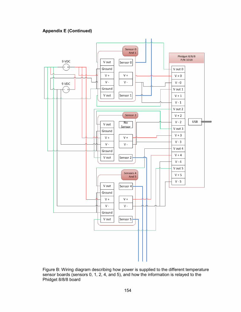
154
Appendix E (Continued)
Figure B: Wiring diagram describing how power is supplied to the different temperature sensor boards (sensors 0, 1, 2, 4, and 5), and how the information is relayed to the Phidget 8/8/8 board

155
Appendix E (Continued)
Figure C: Trace diagram for the temperature sensor circuit boards

156
Appendix F: Control System MATLAB Code
clc clear all
if ~libisloaded('phidget21') loadlibrary phidget21 phidget21Matlab.h end
%% n=0; % initial iteration count v(1)=0; % initial voltage level for sensor 0 v(2)=0; % initial voltage level for sensor 1 v(3)=0; % initial voltage level for sensor 2 v(6)=0; % initial voltage level for sensor 5 p=1; %pause length er=.12; %error percentage reapplied to correct loop jj=180; %iterations desiredT = 66.0000; %desired tempsc=5; % sensor count sc=5; % sensor count ss=sc+1; % sensor count plus one, used for iternation number
%% ptr=libpointer('int32Ptr',0); Tptr = libpointer('int32Ptr',0); % temperature pointer
volptr=libpointer('doublePtr',0); % voltage pointer
if calllib('phidget21', 'CPhidgetAnalog_create', ptr)==0; %verifying
successful creation of pointer fprintf('good analog create\n') handle=get(ptr,'Value'); else fprintf('bad analog create\n') calllib('phidget21', 'CPhidgetAnalog_create', ptr) end
handle=get(ptr,'Value'); %creates handle that retrieves pointer value if calllib('phidget21', 'CPhidget_open', handle, -1)==0; %verify
successful handle operation calllib('phidget21', 'CPhidget_open', handle, -1); fprintf('good volt open\n') else fprintf('bad volt open\n') calllib('phidget21', 'CPhidget_open', handle, -1) end
if calllib('phidget21','CPhidget_waitForAttachment',handle,2500)==0 %
2.5 second wait for Matlab to recognize the device via handle
attachment % n % debugging redundancy, check to see if attachment was
successful % Temperature Control calllib('phidget21', 'CPhidgetInterfaceKit_create', Tptr);

157
Appendix F (Continued)
% Was previously used to verify a good attachment if calllib('phidget21', 'CPhidgetAnalog_getOutputCount', handle,
ptr)==0 fprintf('good output count\n') disp(get(ptr,'Value')); else fprintf('bad output count\n') calllib('phidget21', 'CPhidgetAnalog_getOutputCount', handle, 0) end
handleT = get(Tptr, 'Value'); %creates temp sensor handle that
retrieves pointer value
if calllib('phidget21', 'CPhidget_open', handleT, -1)==0; calllib('phidget21', 'CPhidget_open', handleT, -1); fprintf('good temp open\n') else fprintf('bad temp open\n') calllib('phidget21', 'CPhidget_open', handleT, -1) end
if calllib('phidget21', 'CPhidget_waitForAttachment', handleT, 2500) ==
0 fprintf('good temp sensor wait\n') else calllib('phidget21', 'CPhidgetInterfaceKit_getSensorValue',
handleT, 0, Tptr) disp('Error in temp pointer, get sensor value')
end while n<jj
fprintf('good volt wait\n') calllib('phidget21', 'CPhidgetAnalog_getVoltageMin', handle, 0,
volptr); minVoltage=get(volptr,'Value'); calllib('phidget21', 'CPhidgetAnalog_getVoltageMax', handle, 0,
volptr); maxVoltage=get(volptr,'Value');
%Temp Sensor Readings
if calllib('phidget21', 'CPhidgetInterfaceKit_getSensorValue',
handleT, 0, Tptr) == 0
x = get(Tptr, 'Value'); x= cast (x, 'double'); fprintf('Good temp sensor interface\n') else fprintf('bad temp sensor interface\n')

158
Appendix F (Continued)
calllib('phidget21',
'CPhidgetInterfaceKit_getSensorValue', handleT, 0, Tptr) end
if calllib('phidget21', 'CPhidgetInterfaceKit_getSensorValue',
handleT, 1, Tptr) == 0
x(2) = get(Tptr, 'Value'); x(2)= cast (x(2), 'double'); fprintf('Good temp sensor interface\n') else fprintf('bad temp sensor interface\n') calllib('phidget21',
'CPhidgetInterfaceKit_getSensorValue', handleT, 1, Tptr) end
if calllib('phidget21', 'CPhidgetInterfaceKit_getSensorValue',
handleT, 2, Tptr) == 0
x(3) = get(Tptr, 'Value'); x(3)= cast (x(3), 'double'); fprintf('Good temp sensor interface\n') else fprintf('bad temp sensor interface\n') calllib('phidget21',
'CPhidgetInterfaceKit_getSensorValue', handleT, 2, Tptr) end
if calllib('phidget21', 'CPhidgetInterfaceKit_getSensorValue',
handleT, 4, Tptr) == 0
x(5) = get(Tptr, 'Value'); x(5)= cast (x(5), 'double'); fprintf('Good temp sensor interface\n') else fprintf('bad temp sensor interface\n') calllib('phidget21',
'CPhidgetInterfaceKit_getSensorValue', handleT, 4, Tptr) end
if calllib('phidget21', 'CPhidgetInterfaceKit_getSensorValue',
handleT, 5, Tptr) == 0
x(6) = get(Tptr, 'Value'); x(6)= cast (x(6), 'double'); fprintf('Good temp sensor interface\n') else fprintf('bad temp sensor interface\n') calllib('phidget21',
'CPhidgetInterfaceKit_getSensorValue', handleT, 5, Tptr) end

159
Appendix F (Continued)
%% Temperature Values and Finding Error format long pause(p) % delay "" number of seconds until next iteration actualT(1)= 0.2419*x(1)+31.2475; %sensor 0 actualT(2)= 0.2412*x(2)+29.2405; %sensor 1 actualT(3)= 0.2569*x(3)+45.4281; %sensor 2 actualT(5)= 0.2479*x(5)+32.1083; %sensor 4, ambient air temp actualT(6)= 0.2532*x(6)+45; %sensor 5 error(1)= actualT(1) - desiredT; error(2)= actualT(2) - desiredT; error(3)= actualT(3) - desiredT; error(6)= actualT(6) - desiredT;
%% Inputing Voltage Signal for Each Channel to Reach Desired Temp
v(1)=-6; %v(1)+er*error(1) ; % voltage to sensor 0 v(2)=-6; %v(2)+er*error(2) ; % voltage to sensor 1 v(3)=-6; %v(3)+er*error(3) ; % voltage to sensor 2 v(6)=-6; %v(6)+er*error(6) ; % voltage to sensor 5
%% amp(1)=v(1)/1.5; amp(2)=v(2)/1.5; amp(3)=v(3)/1.5; amp(6)=v(6)/1.5;
calllib('phidget21', 'CPhidgetAnalog_setVoltage',handle, 0, v(1)); calllib('phidget21', 'CPhidgetAnalog_setVoltage',handle, 1, v(2)); calllib('phidget21', 'CPhidgetAnalog_setVoltage',handle, 2, v(3)); calllib('phidget21', 'CPhidgetAnalog_setVoltage',handle, 3, v(6)); calllib('phidget21', 'CPhidgetAnalog_setEnabled',handle, 0, 1); calllib('phidget21', 'CPhidgetAnalog_setEnabled',handle, 1, 1); calllib('phidget21', 'CPhidgetAnalog_setEnabled',handle, 2, 1); calllib('phidget21', 'CPhidgetAnalog_setEnabled',handle, 3, 1);
%% Saftey Measure if abs(v(1)) >= 6.1; v; fprintf('Last measured voltage was %g.\n ',v) v(1)=0; calllib('phidget21', 'CPhidgetAnalog_setVoltage',handle, 0, v(1)); disp('Trying to signal high voltage') break end if abs(v(2)) >= 6.1; v; fprintf('Last measured voltage was %g.\n ',v) v(2)=0; calllib('phidget21', 'CPhidgetAnalog_setVoltage',handle, 0, v(2)); disp('Trying to signal high voltage') break

160
Appendix F (Continued)
end if abs(v(3)) >= 6.1; v; fprintf('Last measured voltage was %g.\n ',v) v(3)=0; calllib('phidget21', 'CPhidgetAnalog_setVoltage',handle, 0, v(3)); disp('Trying to signal high voltage') break end if abs(v(6)) >= 6.1; v; fprintf('Last measured voltage was %g.\n ',v) v(6)=0; calllib('phidget21', 'CPhidgetAnalog_setVoltage',handle, 0, v(6)); disp('Trying to signal high voltage') break end
%% n=n+1; lt=p*n; %lapsed time
time=datestr(now,0); fprintf('\n\nDesired Temp, %g F\n',desiredT) fprintf('Ambient Air Temp, %g F\n',actualT(5)) fprintf('Actual Temp, %g F, %g F, %g F, %g F
\n',actualT(1),actualT(2),actualT(3),actualT(6)) fprintf('Error, %g F, %g F, %g F, %g
F\n',error(1),error(2),error(3),error(6)) fprintf('Voltage Signal, %g V, %g V, %g V, %g
V\n',v(1),v(2),v(3),v(6)) fprintf('Signal Amperage, %g A, %g A, %g A, %g
A\n',amp(1),amp(2),amp(3),amp(6)) fprintf('Iteration Count, %g\n',n) A(:,n)=[p er desiredT actualT(1) actualT(2) actualT(3) actualT(6)
error(1) error(2) error(3) error(6) v(1) v(2) v(3) v(6) amp(1) amp(2)
amp(3) amp(6) lt n]; B(n,:)=[time]; end
if n==jj; v(1)=0; v(2)=0; v(3)=0; v(6)=0; calllib('phidget21', 'CPhidgetAnalog_setVoltage',handle, 0,
v(1)); calllib('phidget21', 'CPhidgetAnalog_setVoltage',handle, 1,
v(2)); calllib('phidget21', 'CPhidgetAnalog_setVoltage',handle, 2,
v(3));

161
Appendix F (Continued)
calllib('phidget21', 'CPhidgetAnalog_setVoltage',handle, 3,
v(6)); end
else fprintf('bad volt wait\n') calllib('phidget21','CPhidget_waitForAttachment',handle,2500) end
actualT calllib('phidget21', 'CPhidget_close', handle); calllib('phidget21', 'CPhidget_delete', handle); calllib('phidget21', 'CPhidget_close', handleT); calllib('phidget21', 'CPhidget_delete', handleT);
% rand xlswrite('C:\Documents and
Settings\camarti9\Desktop\testresult.xls',A,1) xlswrite('C:\Documents and
Settings\camarti9\Desktop\testresult.xls',B,2) %% Error/Problem Log %Its running without the enable code Sept 23rd %Oct 7th, now runs with enable
%Tried to enable other channels with the following code, no repsonse
from %other channels. % calllib('phidget21', 'CPhidgetAnalog_setEnabled',handle, 0, 1); % calllib('phidget21', 'CPhidgetAnalog_setEnabled',handle, 1, 2); % calllib('phidget21', 'CPhidgetAnalog_setEnabled',handle, 2, 3); % calllib('phidget21', 'CPhidgetAnalog_setEnabled',handle, 5, 4);
% calllib('phidget21', 'CPhidgetAnalog_setVoltage',handle, 0, v(1)); % calllib('phidget21', 'CPhidgetAnalog_setVoltage',handle, 1, v(2)); % calllib('phidget21', 'CPhidgetAnalog_setVoltage',handle, 2, v(3)); % calllib('phidget21', 'CPhidgetAnalog_setVoltage',handle, 3, v(6)); % calllib('phidget21', 'CPhidgetAnalog_setEnabled',handle, 0, 1); % calllib('phidget21', 'CPhidgetAnalog_setEnabled',handle, 1, 1); % calllib('phidget21', 'CPhidgetAnalog_setEnabled',handle, 2, 1); % calllib('phidget21', 'CPhidgetAnalog_setEnabled',handle, 5, 1);
% calllib('phidget21', 'CPhidgetAnalog_setVoltage',handle, 0, v(1)); % calllib('phidget21', 'CPhidgetAnalog_setVoltage',handle, 1, v(2)); % calllib('phidget21', 'CPhidgetAnalog_setVoltage',handle, 2, v(3)); % calllib('phidget21', 'CPhidgetAnalog_setVoltage',handle, 3, v(6)); % calllib('phidget21', 'CPhidgetAnalog_setEnabled',handle, 0, 1); % calllib('phidget21', 'CPhidgetAnalog_setEnabled',handle, 1, 1); % calllib('phidget21', 'CPhidgetAnalog_setEnabled',handle, 2, 1); % calllib('phidget21', 'CPhidgetAnalog_setEnabled',handle, 3, 1);

162
Appendix F (Continued)
% calllib('phidget21', 'CPhidgetAnalog_setVoltage',handle, 0, v(1)); % calllib('phidget21', 'CPhidgetAnalog_setVoltage',handle, 1, v(2)); % calllib('phidget21', 'CPhidgetAnalog_setVoltage',handle, 2, v(3)); % calllib('phidget21', 'CPhidgetAnalog_setVoltage',handle, 3, v(6)); % calllib('phidget21', 'CPhidgetAnalog_setEnabled',handle, 0, 1);
%Verified output count still good %Yellow and black wired heat sink is becoming very hot
%Oct 11 Notes % Original Temp Equations % actualT(1)= 0.2419*x(1)+31.2475; %sensor 0 % actualT(2)= 0.2412*x(2)+29.2405; %sensor 1 % actualT(3)= 0.2569*x(3)+45.4281; %sensor 2 % actualT(5)= 0.2479*x(5)+32.1083; %sensor 4, ambient air temp % actualT(6)= 0.2532*x(6)+45; %sensor 5

163
Appendix G: MATLAB Temperature Sensor Measurement Code
clc clear all loadlibrary phidget21 phidget21Matlab.h; % make sure the library is in
your current directory
rand % placed to make sure the code ran a new iteration n=0; sc=5; % sensor count ss=sc+1; % sensor count plus one, used for iternation number format long while n<120 %Create space for interface kit ptr = libpointer('int32Ptr',0); calllib('phidget21', 'CPhidgetInterfaceKit_create', ptr);
handle = get(ptr, 'Value');
calllib('phidget21', 'CPhidget_open', handle, -1);
if calllib('phidget21', 'CPhidget_waitForAttachment', handle, 2500)
== 0
dataptr = libpointer('int32Ptr',0); %get the value, make sure it's valids for i=1:ss b=i-1; if calllib('phidget21',
'CPhidgetInterfaceKit_getSensorValue', handle, b, dataptr) == 0 x(i) = get(dataptr, 'Value'); x = cast (x, 'double'); % converts matrix data
type to double
end end
else disp('Could not open InterfaceKit') % if the
calllib('phidget21', 'CPhidget_waitForAttachment', handle, 2500) ==
something other than 0 than the number is a diagnostic code x=0; end
%Closes phidget connection when finished calllib('phidget21', 'CPhidget_close', handle); calllib('phidget21', 'CPhidget_delete', handle);
%Calculates actual temperature (F) from sensor using conversion actualT(1)= 0.24156*x(1)+31.769; %sensor 0 actualT(2)= 0.23974*x(2)+29.588; %sensor 1 actualT(3)= 0.25024*x(3)+47.043; %sensor 2

164
Appendix G (Continued)
actualT(5)= 0.24498*x(5)+32.907; %sensor 4 actualT(6)= 0.25*x(6)+45.9; %sensor 5
n = n+1; %increase iteration count A(n,:)=[actualT(1) actualT(2) actualT(3) actualT(5) actualT(6)]; %
temperature array fprintf('%5.0f %10.6f %10.6f %10.6f %10.6f %10.6f \n', n,
actualT(1), actualT(2), actualT(3), actualT(5), actualT(6)) % display
temperature array
end % xlswrite('C:\** INSERT FILE LOCATION HERE**.xls',A) % saves data to a
spreadsheet

165
Appendix H: Measured Temperature Profiles of the Final Assembly
H.1 Purple Channel
Figure D: Underside purple channel temperature profile at 0.5 amps
Figure E: Topside purple channel temperature profile at 0.5 amps
74
75
76
77
78
79
80
81
82
83 1
7
1
3
19
2
5
31
3
7
43
4
9
55
6
1
67
7
3
79
8
5
91
9
7
10
3
10
9
11
5
Tem
pe
ratu
re (
°F)
Time (s)
Underside Purple Channel, 0.5 A
Left Sensor
Center Sensor
Right Sensor
67
67.5
68
68.5
69
69.5
70
70.5
71
71.5
72
1
8
15
22
29
36
43
50
57
64
71
78
85
92
99
10
6
11
3
12
0
Tem
pe
ratu
re (
°F)
Time (s)
Topside Purple Channel, 0.5 A
Left Sensor
Right Sensor
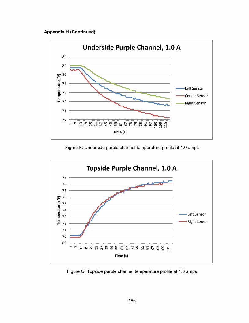
166
Appendix H (Continued)
Figure F: Underside purple channel temperature profile at 1.0 amps
Figure G: Topside purple channel temperature profile at 1.0 amps
70
72
74
76
78
80
82
84
1
7
13
1
9
25
3
1
37
4
3
49
5
5
61
6
7
73
7
9
85
9
1
97
1
03
1
09
1
15
Tem
pe
ratu
re (
°F)
Time (s)
Underside Purple Channel, 1.0 A
Left Sensor
Center Sensor
Right Sensor
69
70
71
72
73
74
75
76
77
78
79
1
7
13
19
25
31
37
43
49
55
61
67
73
79
85
91
97
10
3
10
9
11
5
Tem
pe
ratu
re (
°F)
Time (s)
Topside Purple Channel, 1.0 A
Left Sensor
Right Sensor
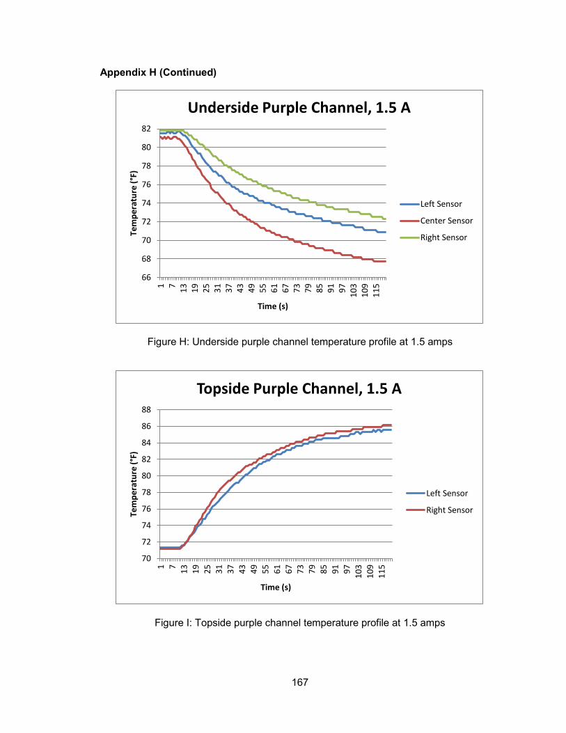
167
Appendix H (Continued)
Figure H: Underside purple channel temperature profile at 1.5 amps
Figure I: Topside purple channel temperature profile at 1.5 amps
66
68
70
72
74
76
78
80
82
1
7
13
1
9
25
3
1
37
4
3
49
5
5
61
6
7
73
7
9
85
9
1
97
1
03
1
09
1
15
Tem
pe
ratu
re (
°F)
Time (s)
Underside Purple Channel, 1.5 A
Left Sensor
Center Sensor
Right Sensor
70
72
74
76
78
80
82
84
86
88
1
7
13
19
25
31
37
43
49
55
61
67
73
79
85
91
97
10
3
10
9
11
5
Tem
pe
ratu
re (
°F)
Time (s)
Topside Purple Channel, 1.5 A
Left Sensor
Right Sensor

168
Appendix H (Continued)
Figure J: Underside purple channel temperature profile at 2.0 amps
Figure K: Topside purple channel temperature profile at 2.0 amps
66
68
70
72
74
76
78
80
82
84
1
7
13
1
9
25
3
1
37
4
3
49
5
5
61
6
7
73
7
9
85
9
1
97
1
03
1
09
1
15
Tem
pe
ratu
re (
°F)
Time (s)
Underside Purple Channel, 2.0 A
Left Sensor
Center Sensor
Right Sensor
70
75
80
85
90
95
100
1
7
13
1
9
25
3
1
37
4
3
49
5
5
61
6
7
73
7
9
85
9
1
97
1
03
1
09
1
15
Tem
pe
ratu
re (
°F)
Time (s)
Topside Purple Channel, 2.0 A
Left Sensor
Right Sensor
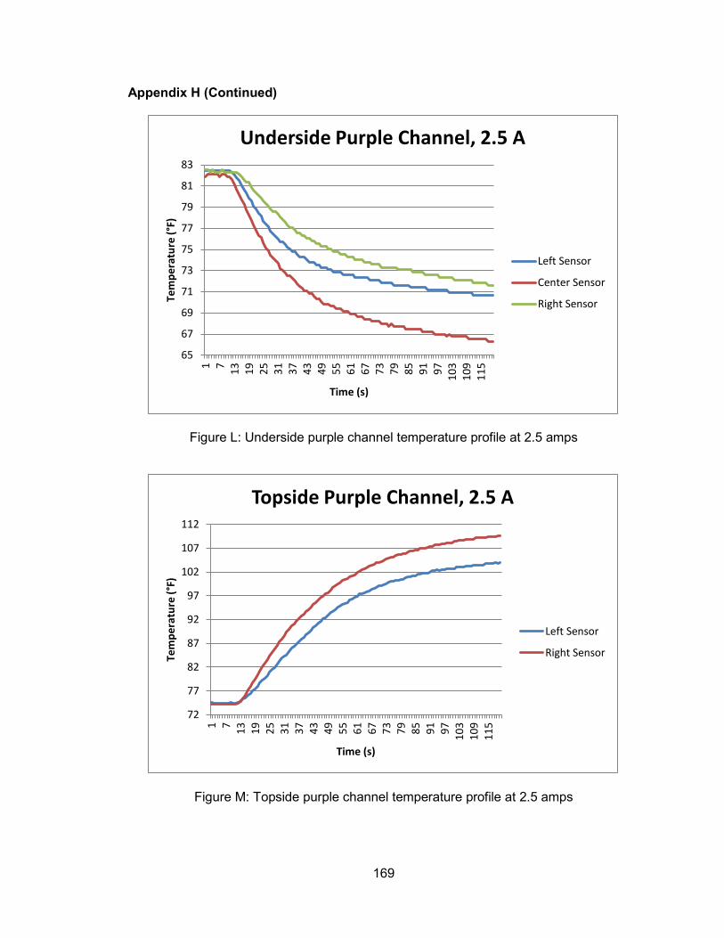
169
Appendix H (Continued)
Figure L: Underside purple channel temperature profile at 2.5 amps
Figure M: Topside purple channel temperature profile at 2.5 amps
65
67
69
71
73
75
77
79
81
83
1
7
13
1
9
25
3
1
37
4
3
49
5
5
61
6
7
73
7
9
85
9
1
97
1
03
1
09
1
15
Tem
pe
ratu
re (
°F)
Time (s)
Underside Purple Channel, 2.5 A
Left Sensor
Center Sensor
Right Sensor
72
77
82
87
92
97
102
107
112
1
7
13
1
9
25
3
1
37
4
3
49
5
5
61
6
7
73
7
9
85
9
1
97
1
03
1
09
1
15
Tem
pe
ratu
re (
°F)
Time (s)
Topside Purple Channel, 2.5 A
Left Sensor
Right Sensor

170
Appendix H (Continued)
H.2 Yellow Channel
Figure N: Underside yellow channel temperature profile at 0.5 amps
Figure O: Topside yellow channel temperature profile at 0.5 amps
71
72
73
74
75
76
77 1
7
1
3
19
2
5
31
3
7
43
4
9
55
6
1
67
7
3
79
8
5
91
9
7
10
3
10
9
11
5
Tem
pe
ratu
re (
°F)
Time (s)
Underside Yellow Channel, 0.5 A
Left Sensor
Center Sensor
Right Sensor
60
62
64
66
68
70
72
74
76
1
7
13
19
25
31
37
43
49
55
61
67
73
79
85
91
97
10
3
10
9
11
5
Tem
pe
ratu
re (
°F)
Time (s)
Topside Yellow Channel, 0.5 A
Left Sensor
Right Sensor

171
Appendix H (Continued)
Figure P: Underside yellow channel temperature profile at 1.0 amps
Figure Q: Topside yellow channel temperature profile at 1.0 amps
69
70
71
72
73
74
75
76
77
1
7
13
1
9
25
3
1
37
4
3
49
5
5
61
6
7
73
7
9
85
9
1
97
1
03
1
09
1
15
Tem
pe
ratu
re (
°F)
Time (s)
Underside Yellow Channel, 1.0 A
Left Sensor
Center Sensor
Right Sensor
62
64
66
68
70
72
74
76
78
80
82
1
7
13
19
25
31
37
43
49
55
61
67
73
79
85
91
97
10
3
10
9
11
5
Tem
pe
ratu
re (
°F)
Time (s)
Topside Yellow Channel, 1.0 A
Left Sensor
Right Sensor

172
Appendix H (Continued)
Figure R: Underside yellow channel temperature profile at 1.5 amps
Figure S: Topside yellow channel temperature profile at 1.5 amps
68
69
70
71
72
73
74
75
76
77
78
1
7
13
1
9
25
3
1
37
4
3
49
5
5
61
6
7
73
7
9
85
9
1
97
1
03
1
09
1
15
Tem
pe
ratu
re (
°F)
Time (s)
Underside Yellow Channel, 1.5 A
Left Sensor
Center Sensor
Right Sensor
65
70
75
80
85
90
1
7
13
19
25
31
37
43
49
55
61
67
73
79
85
91
97
10
3
10
9
11
5
Tem
pe
ratu
re (
°F)
Time (s)
Topside Yellow Channel, 1.5 A
Left Sensor
Right Sensor

173
Appendix H (Continued)
Figure T: Underside yellow channel temperature profile at 2.0 amps
Figure U: Topside yellow channel temperature profile at 2.0 amps
69
70
71
72
73
74
75
76
77
78
79
1
7
13
1
9
25
3
1
37
4
3
49
5
5
61
6
7
73
7
9
85
9
1
97
1
03
1
09
1
15
Tem
pe
ratu
re (
°F)
Time (s)
Underside Yellow Channel, 2.0 A
Left Sensor
Center Sensor
Right Sensor
65
70
75
80
85
90
95
100
105
1
7
13
1
9
25
3
1
37
4
3
49
5
5
61
6
7
73
7
9
85
9
1
97
1
03
1
09
1
15
Tem
pe
ratu
re (
°F)
Time (s)
Topside Yellow Channel, 2.0 A
Left Sensor
Right Sensor

174
Appendix H (Continued)
Figure V: Underside yellow channel temperature profile at 2.5 amps
Figure W: Topside yellow channel temperature profile at 2.5 amps
70
72
74
76
78
80
82
1
7
13
1
9
25
3
1
37
4
3
49
5
5
61
6
7
73
7
9
85
9
1
97
1
03
1
09
1
15
Tem
pe
ratu
re (
°F)
Time (s)
Underside Yellow Channel, 2.5 A
Left Sensor
Center Sensor
Right Sensor
65
70
75
80
85
90
95
100
105
110
115
120
1
7
13
1
9
25
3
1
37
4
3
49
5
5
61
6
7
73
7
9
85
9
1
97
1
03
1
09
1
15
Tem
pe
ratu
re (
°F)
Time (s)
Topside Yellow Channel, 2.5 A
Left Sensor
Right Sensor

175
Appendix H (Continued)
H.3 Blue Channel
Figure X: Underside blue channel temperature profile at 0.5 amps
Figure Y: Topside blue channel temperature profile at 0.5 amps
73
74
75
76
77
78
79
80 1
7
1
3
19
2
5
31
3
7
43
4
9
55
6
1
67
7
3
79
8
5
91
9
7
10
3
10
9
11
5
Tem
pe
ratu
re (
°F)
Time (s)
Underside Blue Channel, 0.5 A
Left Sensor
Center Sensor
Right Sensor
58
60
62
64
66
68
70
72
74
1
7
13
19
25
31
37
43
49
55
61
67
73
79
85
91
97
10
3
10
9
11
5
Tem
pe
ratu
re (
°F)
Time (s)
Topside Blue Channel, 0.5 A
Left Sensor
Right Sensor
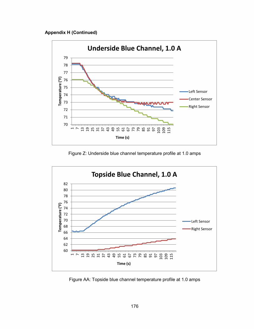
176
Appendix H (Continued)
Figure Z: Underside blue channel temperature profile at 1.0 amps
Figure AA: Topside blue channel temperature profile at 1.0 amps
70
71
72
73
74
75
76
77
78
79
1
7
13
1
9
25
3
1
37
4
3
49
5
5
61
6
7
73
7
9
85
9
1
97
1
03
1
09
1
15
Tem
pe
ratu
re (
°F)
Time (s)
Underside Blue Channel, 1.0 A
Left Sensor
Center Sensor
Right Sensor
60
62
64
66
68
70
72
74
76
78
80
82
1
7
13
19
25
31
37
43
49
55
61
67
73
79
85
91
97
10
3
10
9
11
5
Tem
pe
ratu
re (
°F)
Time (s)
Topside Blue Channel, 1.0 A
Left Sensor
Right Sensor

177
Appendix H (Continued)
Figure BB: Underside blue channel temperature profile at 1.5 amps
Figure CC: Topside blue channel temperature profile at 1.5 amps
67
68
69
70
71
72
73
74
75
76
77
78
79
1
7
13
1
9
25
3
1
37
4
3
49
5
5
61
6
7
73
7
9
85
9
1
97
1
03
1
09
1
15
Tem
pe
ratu
re (
°F)
Time (s)
Underside Blue Channel, 1.5 A
Left Sensor
Center Sensor
Right Sensor
60
64
68
72
76
80
84
88
92
1
7
13
19
25
31
37
43
49
55
61
67
73
79
85
91
97
10
3
10
9
11
5
Tem
pe
ratu
re (
°F)
Time (s)
Topside Blue Channel, 1.5 A
Left Sensor
Right Sensor

178
Appendix H (Continued)
Figure DD: Underside blue channel temperature profile at 2.0 amps
Figure EE: Topside blue channel temperature profile at 2.0 amps
66 67 68 69 70 71 72 73 74 75 76 77 78 79 80
1
7
13
1
9
25
3
1
37
4
3
49
5
5
61
6
7
73
7
9
85
9
1
97
1
03
1
09
1
15
Tem
pe
ratu
re (
°F)
Time (s)
Underside Blue Channel, 2.0 A
Left Sensor
Center Sensor
Right Sensor
60
65
70
75
80
85
90
95
100
105
1
7
13
1
9
25
3
1
37
4
3
49
5
5
61
6
7
73
7
9
85
9
1
97
1
03
1
09
1
15
Tem
pe
ratu
re (
°F)
Time (s)
Topside Blue Channel, 2.0 A
Left Sensor
Right Sensor

179
Appendix H (Continued)
Figure FF: Underside blue channel temperature profile at 2.5 amps
Figure GG: Topside blue channel temperature profile at 2.5 amps
66 67 68 69 70 71 72 73 74 75 76 77 78 79 80
1
7
13
1
9
25
3
1
37
4
3
49
5
5
61
6
7
73
7
9
85
9
1
97
1
03
1
09
1
15
Tem
pe
ratu
re (
°F)
Time (s)
Underside Blue Channel, 2.5 A
Left Sensor
Center Sensor
Right Sensor
62
72
82
92
102
112
122
1
7
13
1
9
25
3
1
37
4
3
49
5
5
61
6
7
73
7
9
85
9
1
97
1
03
1
09
1
15
Tem
pe
ratu
re (
°F)
Time (s)
Topside Blue Channel, 2.5 A
Left Sensor
Right Sensor

180
Appendix H (Continued)
H.4 Green Channel
Figure HH: Underside green channel temperature profile at 0.5 amps
Figure II: Topside green channel temperature profile at 0.5 amps
68
69
70
71
72
73
74
75
76
77
78 1
7
1
3
19
2
5
31
3
7
43
4
9
55
6
1
67
7
3
79
8
5
91
9
7
10
3
10
9
11
5
Tem
pe
ratu
re (
°F)
Time (s)
Underside Green Channel, 0.5 A
Left Sensor
Center Sensor
Right Sensor
62
64
66
68
70
72
74
1
7
13
19
25
31
37
43
49
55
61
67
73
79
85
91
97
10
3
10
9
11
5
Tem
pe
ratu
re (
°F)
Time (s)
Topside Green Channel, 0.5 A
Left Sensor
Right Sensor
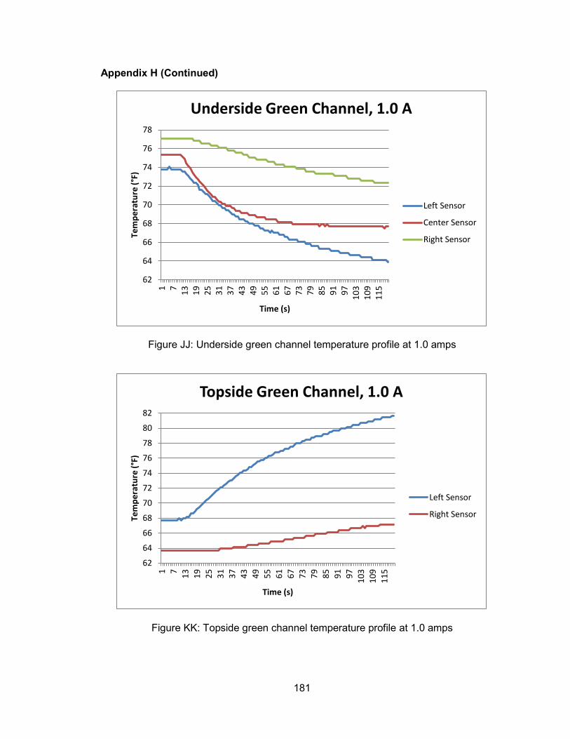
181
Appendix H (Continued)
Figure JJ: Underside green channel temperature profile at 1.0 amps
Figure KK: Topside green channel temperature profile at 1.0 amps
62
64
66
68
70
72
74
76
78
1
7
13
1
9
25
3
1
37
4
3
49
5
5
61
6
7
73
7
9
85
9
1
97
1
03
1
09
1
15
Tem
pe
ratu
re (
°F)
Time (s)
Underside Green Channel, 1.0 A
Left Sensor
Center Sensor
Right Sensor
62
64
66
68
70
72
74
76
78
80
82
1
7
13
19
25
31
37
43
49
55
61
67
73
79
85
91
97
10
3
10
9
11
5
Tem
pe
ratu
re (
°F)
Time (s)
Topside Green Channel, 1.0 A
Left Sensor
Right Sensor

182
Appendix H (Continued)
Figure LL: Underside green channel temperature profile at 1.5 amps
Figure MM: Topside green channel temperature profile at 1.5 amps
59
61
63
65
67
69
71
73
75
77
79
1
7
13
1
9
25
3
1
37
4
3
49
5
5
61
6
7
73
7
9
85
9
1
97
1
03
1
09
1
15
Tem
pe
ratu
re (
°F)
Time (s)
Underside Green Channel, 1.5 A
Left Sensor
Center Sensor
Right Sensor
64
69
74
79
84
89
94
1
7
13
19
25
31
37
43
49
55
61
67
73
79
85
91
97
10
3
10
9
11
5
Tem
pe
ratu
re (
°F)
Time (s)
Topside Green Channel, 1.5 A
Left Sensor
Right Sensor

183
Appendix H (Continued)
Figure NN: Underside green channel temperature profile at 2.0 amps
Figure OO: Topside green channel temperature profile at 2.0 amps
57
60
63
66
69
72
75
78
1
7
13
1
9
25
3
1
37
4
3
49
5
5
61
6
7
73
7
9
85
9
1
97
1
03
1
09
1
15
Tem
pe
ratu
re (
°F)
Time (s)
Underside Green Channel, 2.0 A
Left Sensor
Center Sensor
Right Sensor
64
69
74
79
84
89
94
99
104
1
7
13
1
9
25
3
1
37
4
3
49
5
5
61
6
7
73
7
9
85
9
1
97
1
03
1
09
1
15
Tem
pe
ratu
re (
°F)
Time (s)
Topside Green Channel, 2.0 A
Left Sensor
Right Sensor

184
Appendix H (Continued)
Figure PP: Underside green channel temperature profile at 2.5 amps
Figure QQ: Topside green channel temperature profile at 2.5 amps
56
58
60
62
64
66
68
70
72
74
76
78
80
1
7
13
1
9
25
3
1
37
4
3
49
5
5
61
6
7
73
7
9
85
9
1
97
1
03
1
09
1
15
Tem
pe
ratu
re (
°F)
Time (s)
Underside Green Channel, 2.5 A
Left Sensor
Center Sensor
Right Sensor
65
70
75
80
85
90
95
100
105
110
115
120
1
7
13
1
9
25
3
1
37
4
3
49
5
5
61
6
7
73
7
9
85
9
1
97
1
03
1
09
1
15
Tem
pe
ratu
re (
°F)
Time (s)
Topside Green Channel, 2.5 A
Left Sensor
Right Sensor