
Design, Implementation, and Analysis for an Improved ... · Design, Implementation, and Analysis...
152
Design, Implementation, and Analysis for an Improved Multiple Inverter Microgrid System Chien-Liang Chen Dissertation submitted to the faculty of the Virginia Polytechnic Institute and State University in partial fulfillment of the requirements for the degree of Doctor of Philosophy In Electrical Engineering Jih-Sheng Lai, Chair William T. Baumann Virgilio A. Centeno Kathleen Meehan Douglas J. Nelson February 04, 2011 Blacksburg, Virginia Key words: Microgrid, mode transfer, grid-tie mode, islanding mode, stability Copyright 2011, Chien-Liang Chen
Transcript of Design, Implementation, and Analysis for an Improved ... · Design, Implementation, and Analysis...

Design, Implementation, and Analysis for an Improved Multiple Inverter
Microgrid System
Chien-Liang Chen
Dissertation submitted to the faculty of the Virginia Polytechnic Institute and State University
in partial fulfillment of the requirements for the degree of
Doctor of Philosophy In
Electrical Engineering
Jih-Sheng Lai, Chair William T. Baumann Virgilio A. Centeno Kathleen Meehan Douglas J. Nelson
February 04, 2011 Blacksburg, Virginia
Key words: Microgrid, mode transfer, grid-tie mode, islanding mode, stability
Copyright 2011, Chien-Liang Chen

Design, Implementation, and Analysis for an Improved Multiple Inverter
Microgrid System
Chien-Liang Chen
ABSTRACT
Distributed generation (DG) is getting more and more popular due to the
environmentally-friendly feature, the new generation unit developments, and the ability to
operate in a remote area. By clustering the paralleled DGs, storage system and loads, a
microgrid (MG) can offer a power system with increased reliability, flexibility, cost
effectiveness, and energy efficient feature. Popular energy sources like photovoltaic
modules (PV), wind turbines, and fuel cells require the power-electronic interface as the
bridge to connect to the utility grid for usable transmission.
The inverter-based microgrid system, however, suffers more challenges than
traditional rotational power system. Those challenges, including much less over current
capability, the nature of the intermittent renewable energy sources, a wide-band dynamic
of generation units, and a large grid impedance variation, call for more careful system
hardware and control designs to ensure a reliable system operation. Major design interests
are found in (i) precision power flow control, (ii) proper current sharing, (iii) smooth
transition between grid-tie and islanding modes, and (iv) stability analysis.
This dissertation will cover a complete design and implementation of an
experimental microgrid with paralleled power conditioning systems operating in the grid-
tie mode, islanding mode, and mode transfers. A universal inverter is proposed with the
LCL filter to operate in both grid-tie and standalone mode without any hardware
modification.
iii
Next, controllers of individual inverters running in basic microgrid modes will be
discussed to ensure high quality output characteristics. The admittance compensation will
also be proposed to avoid reverse power flow during the grid-tie connection transient.
Combining previous designed single inverters, a CAN-bus multi-inverter microgrid
system will be established. The current sharing with the proposed frequency-decoupled
transmission will be implemented to extend the transmission distance. Next, smooth mode
transfer procedures between grid-tie mode and islanding mode will be suggested based on
the circuit principles to minimize the excessive electrical stresses. Finally, the state-space
analysis of the proposed multi-inverter microgrid system will be conducted to investigate
the stability under system variations and optimize the system performance.
Experimental and simulation results show that the designed universal inverter can
provide stable outputs in different basic microgrid operation modes. With the proposed
current sharing scheme, the output current is equally shared among paralleled inverters
without a noticeable circulating current. Both the simulation and experimental results of
mode transfer show that the multi-inverter based microgrid system is able to switch
between grid-tie and islanding modes smoothly to guarantee an uninterrupted power
supply to the critical loads. Based on eigenvalue analysis, the study of stability analysis
also shows the agreement of the design, simulation and test results which further verifies
the reliability of the designed multi-inverter microgrid system.

iv
To my parents
Yu-Tang Chen and Po-Quai Huang
To my grandparents
Zhang- Cheng Chen and Chan Xie
To my wife
Shu-Hui Liu

v
Acknowledgements
I would like to express my most sincere gratitude and appreciation to my advisor,
Dr. Jason Lai, for his constant support and guidance throughout the course of this work at
Virginia Tech. His valuable expertise, advices, and encouragements have been a source of
this work throughout the years.
I would like to thank Dr. William Baumann, Dr. Virgilio Centeno, Dr. Kathleen
Meehan, and Dr. Douglas Nelson for serving as members of my committee, and for their
interests, suggestions and kind supports for this work.
I would also like to thank the Future Energy Electronics Center (FEEC) colleagues,
Mr. Gary Kerr, Mr. Wensong Yu, Mr. Sung-Yeul Park, Mr. Seungryul Moon, Mr. Rae-
Young Kim, Ms. Junhong Zhang, Mr. Daniel Martin, Mr. Hidekazu Miwa, Mr. Young
Hoon Cho, Mr. Pengwei Sun, Mr. Hao Qian, Mr. Brett Whitaker, Mr. Baifeng Chen, Mr.
Zakariya Dalala, Mr. Ahmed Koran, Mr. Zidong Liu, Mr. Chris Hutchens, Mr. Ben York,
Mr. Alex Kim, Mr. Hsin Wang, Mr. Cong Zheng, Mr. Bin Gu, Mr. Thomas LaBella, Ms.
Hongmei Wan, Ms. Zheng Zhao, Mr. Zaka Ullah Zahid, Ms. Nanying Yang, Ms. Hyun
Soo Koh, Mr. Konstantin Louganski, Mr. Neil Savio D’Souza, Mr. Ken Stanton, and Mr.
Edward Jones. My study and research were enjoyable and valuable experiences with their
helpful discussions, great supports and precious friendship. My gratitude needs to go to
the visiting scholars, Mr. Yuang-Shung Lee, Mr. Yu-Bin Wang, Mr. Huang-Jen Chiu, Mr.

vi
Kuan-Hung Wu, Mr. Chuang Liu, Hong-Po Ma, and Mr. Sano Kenichiro for their kindly
suggestions and help on my research. I also want to give thanks to Department of Energy,
USA, Institute of Nuclear Energy Research, Atomic Energy Council, Taiwan and Tatung
System Technologies, Taipei, Taiwan for the financial and technical supports of the
projects.
With my heartfelt respect, I thank my father, Mr. Yu-Tang Chen, mother, Ms. Po-
Quai Huang, grandfather, Mr. Zhang-Cheng Chen, and grandmother, Ms. Chan Xie. for
their everlasting love, support and care. Without them, I could not have finished this
achievement. Finally, I would like to specially thank my wife, Ms. Shu-Hui Liu, who has
always been there with her understanding, support, and encouragement. Without her, I
may lose the motivation to work for my future. My family is my eternal source of
inspiration in every aspect and every moment in my life.

vii
Table of Contents
Chapter 1 Introduction ............................................................................................... 1
1.1 Research background................................................................................................ 1
1.2 Precision power flow control ..................................................................................... 7
1.3 Current sharing in islanding mode............................................................................ 11
1.4 Mode transfers between grid-tie and islanding modes................................................ 13
1.5 Modeling and stability analysis................................................................................ 15
1.6 Research motivations and objectives ........................................................................ 18
1.7 Dissertation outline................................................................................................. 20
Chapter 2 Single Universal Inverter with Both Grid-tie and Standalone Operations 22
2.1 Introduction ........................................................................................................... 22
2.2 Grid-tie inverter control system modeling................................................................. 24
2.3 Admittance compensation ....................................................................................... 29
2.4 LCL filter design for universal inverter .................................................................... 33
2.5 Current proportional-resonant controller design in grid-tie inverter ............................ 38
2.6 Voltage dual-loop controller design in standalone inverter ......................................... 42
2.7 Phase-lock loop for synchronization......................................................................... 47
2.8 Simulation and experimental verification ................................................................. 50
2.9 Summary ............................................................................................................... 59

viii
Chapter 3 Current Sharing and Smooth Mode Transfer of Parallel Inverters in
Microgrid Applications ....................................................................................... 61
3.1 Introduction ........................................................................................................... 61
3.2 Basic microgrid operations with LCL parallel inverters ............................................. 63
3.3 Current sharing and synchronization through CAN bus ............................................. 68
3.4 Mode transfer considerations Performance evaluation of generalized control structure 71
3.5 Simulation and experimental verification ................................................................. 74
3.6 Summary ............................................................................................................... 86
Chapter 4 State-Space Modeling, Analysis, and Implementation of Paralleled Inverters
for Microgrid Applications .................................................................................. 88
4.1 Introduction ........................................................................................................... 88
4.2 Modeling and analysis of single inverter in grid-tie mode.......................................... 89
4.3 Modeling and analysis of single inverter in standalone mode ..................................... 98
4.4 Modeling and analysis of parallel inverters with the current sharing controller.......... 102
4.5 Simulation and experimental verification ............................................................... 108
4.6 Summary ............................................................................................................. 121
Chapter 5 Conclusion and Future Works ................................................................. 123
5.1 Summary and major contributions ......................................................................... 123
5.2 Future works ........................................................................................................ 125
5.3 Publications ......................................................................................................... 125
References ................................................................................................................ 128
ix
List of Figures
Fig. 1.1 Typical microgrid architecture.......................................................................... 4
Fig. 2.1 (a) Inverter control system of a L-filter-based fuel cell PCS, and (b) V6 dc-dc converter circuit topology, (c) full-bridge inverter circuit topology, and (d) inverter control diagram using transfer functions........................................... 25
Fig. 2.2 (a) Current reference correction method, and (b) admittance compensation method.. .......................................................................................................... 30
Fig. 2.3 (a) Equivalent control block diagram for a grid-tie inverter, (b) power circuit diagram for a grid-tie inverter, and (c) power circuit diagram for a grid-tie inverter with admittance compensation.......................................................... 32
Fig. 2.4 (a) L and LCL filter to achieve same ripple attenuation, (b) system block diagram of a universal inverter using LCL filter, (c) standalone mode, and (d) utility grid-tie mode... ............................................................................................................. 34
Fig. 2.5 Block diagram of the complete admittance compensated LCL-filter based grid-tie inverter.. ............................................................................................. 37
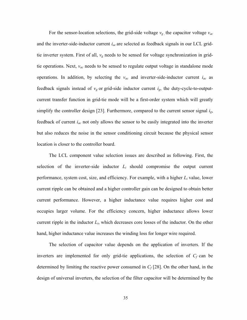
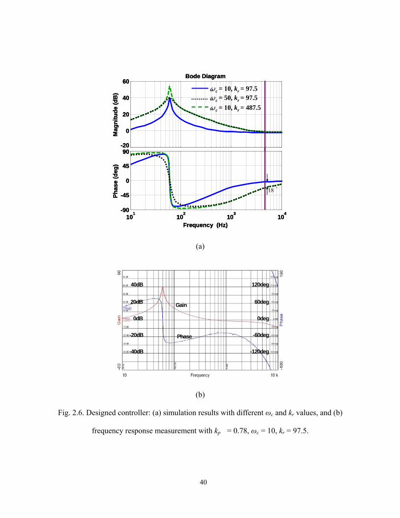
Fig. 2.6 Designed controller: (a) simulation results with different ωc and kr values, and (b) frequency response measurement with kp = 0.78, ωc = 10, kr = 97.5.. ... 40
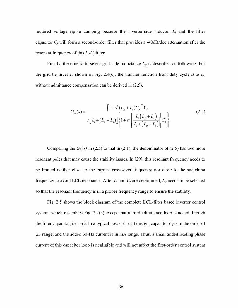
Fig. 2.7 Current loop gain plot showing crossover frequency of 1.46kHz and phase margin of 63.2°... ............................................................................................ 41
Fig. 2.8 Control block diagram of a voltage dual-loop controlled inverter. ................ 45
Fig. 2.9 The Bode plots of voltage controller designs (a) current loop results, and (b) voltage loop results......................................................................................... 46
Fig. 2.10 Phase-lock loop with the peak-value calculation (a) control block diagram, and (b) PLL loop plot showing crossover frequency of 28Hz and phase margin of 36°. ................................................................................................. 49
Fig. 2.11 Simulation results of phase-lock loop and peak value calculation.. ............... 51
Fig. 2.12 Photograph of a fuel cell PCS prototype under test........................................ 52
Fig. 2.13 Pspice simulation results at zero power command start-up (a) with Gc(s) compensation, and (b) without Gc(s) compensation....................................... 54
Fig. 2.14 Experimental results at zero power command start-up (a) without Gc(s) compensation, and (b) with Gc(s) compensation............................................ 55
x
Fig. 2.15 Current loop implementation results at 4.85kW (a) Pspice simulation result at 32A iref, pk, , and (b) experimental result at 32A iref, pk. ................................ 57
Fig. 2.16 Voltage dual-loop results at 215V vac, rms, 5.2kW (a) Pspice simulation result, and (b) experimental result. ............................................................................ 58
Fig. 3.1 The hardware configuration of parallel-inverter microgird system................ 65
Fig. 3.2 Control block diagrams of the parallel-inverter microgrid system in islanding mode. .............................................................................................................. 66
Fig. 3.3 Control block diagrams of the parallel-inverter microgrid system in grid-tie mode. .............................................................................................................. 67
Fig. 3.4 Photograph of the proposed microgrid system. .............................................. 76
Fig. 3.5 Islanding mode operation by designed parallel-inverter system at 215V vload,
rms, 7.6kW (a) Pspice simulation result, and (b) experimental result.............. 77
Fig. 3.6 Grid-tie mode to islanding mode transfer simulation results. ........................ 80
Fig. 3.7 Grid-tie mode to islanding mode transfer experimental results. .................... 81
Fig. 3.8 Bus voltage synchronization transition before the micorgrid reconnecting to the grid............................................................................................................ 83
Fig. 3.9 Islanding mode to grid-tie mode transfer simulation results. ......................... 84
Fig. 3.10 Islanding mode to grid-tie mode transfer experimental results. ..................... 85
Fig. 4.1 Single inverter hardware configuration: (a) grid-tie mode, and (b) standalone mode ............................................................................................................... 90
Fig. 4.2 Control block diagrams of a single inverter in grid-tie mode with admittance compensation.................................................................................................. 91
Fig. 4.3 Control block diagrams of the phase-lock loop with the peak-value calculation....................................................................................................... 94
Fig. 4.4 Eigenvalue of grid-tie inverter (a) complete eigenvalue for kpg = 0.78, and (b) the critical eigenvalue changes with varying kpg from 0.78 to 16. ................. 97
Fig. 4.5 Control block diagrams of a single inverter in standalone mode with admittance compensation. .............................................................................. 99
Fig. 4.6 Eigenvalue of standalone inverter (a) complete eigenvalue for kpg = 0.02, and (b) the critical eigenvalue changes with the varying kpg and load Rload........ 101
Fig. 4.7 The hardware of parallel-inverter microgrid system in islanding mode. ..... 104
xi
Fig. 4.8 The control block diagram of parallel-inverter microgrid system in islanding mode. ............................................................................................................ 105
Fig. 4.9 Eigenvalues of the microgrid system in islanding mode (a) complete eigenvalues for Rload = 27 Ω, and (b) the critical mode eigenvalue changes with varying Rload.......................................................................................... 107
Fig. 4.10 Grid-tie mode results at 3.2 kW with kpg = 0.78 and krg = 97.5 (a) simulation results, and (b) experimental results. ............................................................ 109
Fig. 4.11 Transient grid-tie mode results from 1.8 kW to 3.6kW with kpg = 0.78 and krg = 97.5 (a) simulation results, and (b) experimental results. ......................... 110
Fig. 4.12 Grid-tie mode results at 3.2 kW with kpg = 16 and krg = 97.5 (a) time-domain simulation result, (b) zoom in time-domain result (c) frequency spectrum of time-domain waveform, and (d) the bode plot of current loop . .................. 111
Fig. 4.13 Standalone mode results at 3.2 kW with kps = 0.02 and krs = 12 (a) simulation results, and (b) experimental results. ............................................................ 114
Fig. 4.14 Transient standalone mode results from Rload = 27 Ω to Rload = 13.5 Ω with kp = 0.02 and krs = 12 (a) simulation results, and (b) experimental results. ..... 115
Fig. 4.15 Transient standalone simulation results from Rload = 27 Ω to Rload = 13.5 Ωwith kps = 2 and krs = 12............................................................................. 116
Fig. 4.16 Simulation results of the microgrid system in islanding mode (a) Pout = 800 W (Rload = 54 Ω) and, (b) Pout = 7.4 kW (Rload = 6 Ω). .................................... 118
Fig. 4.17 Experimental results of the microgrid system in islanding mode (a) Pout = 800 W (Rload = 54 Ω) and, (b) Pout = 7.4 kW (Rload = 6 Ω)................................. 119
Fig. 4.18 Transient results of the microgrid system in islanding mode from Rload = 27 Ω to Rload = 13.5 Ω (a) simulation results, and (b) experimental results. ......... 120

xii
List of Table
Table 3.1 Maximum signal rates for various cable lengths of CAN bus………………….70
1
Chapter 1
Introduction
1.1 Research background
In the past few decades, distributed generation (DG) [1]-[4] has gained lots of
attention due to the environmentally-friendly feature of alternative energy, the
development of new generation units, and its ability to offer more options of price-quality
combination to meet the changing electricity market. DG units provide power in the
vicinity of loads, which reduces the losses during power transmission and improves the
power quality to the loads. Furthermore, the DG units can also be utilized in a remote area
where the grid is not reachable, or it can be used as a backup source when the grid is not
available.
Photovoltaic modules (PV) [5], and wind turbines [6], fuel cells [7], Microturbines
[8] are commonly used as the sources for the DG units. Because the first two energy
sources do not require purchasing fuel and their installation cost falls in the order of $1/W,
the installation of PV and wind turbines increased at a rate of 20-40% per year in the last
few years [9]-[10]. Even though fuel cells and microturbines have a higher fuel cost
compared to the first two energy sources, they are preferable for the system stability
because they do not rely on the weather for power production.

2
In order to utilize the energy resources efficiently, the DG units can also be
powered by a hybrid generation systems [11]-[12]. Two types of hybrid system are
available: (1) combining a high temperature fuel cell and other thermal-related energy
sources to increase the system efficiency, (2) incorporating intermittent DG sources and
rechargeable DG sources to extract the most available energy. A high-temperature solid-
oxide-fuel-cell-gas-turbine system and a PV-wind-fuel-cell system belong to the first type
and the second type, respectively.
If DG units are powered by intermittent energy sources only, such as PV or wind,
and supply a local load without connecting to the utility grid, it is necessary for DG units
to have the storage devices to handle the transient energy demands. These storage devices
include batteries, flywheels, super-capacitors, hydrogen, compressed air, pumped-
hydroelectric storage and super-conducting magnetic energy storage devices (SMES) [12]-
[13].
A typical microgrid system (MG) consists of paralleled distributed generation units,
storage systems, and a cluster of loads within a local area [14]-[17]. Microgrids not only
have the inherited advantages of DG but also can offer several substantial benefits
including: increased reliability from the redundant configuration of paralleled DG units;
flexible, cost effective, and energy efficient features by power management and control.

3
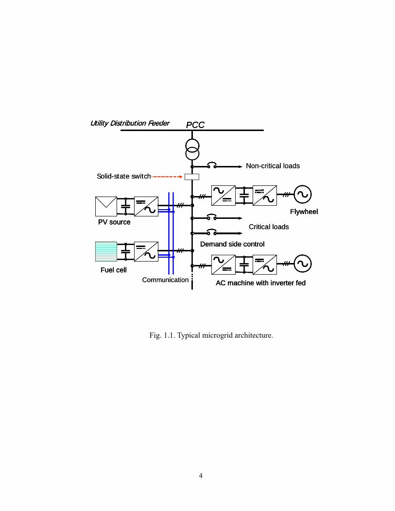
As shown in Fig. 1.1, a microgrid can be operated in both grid-tie and islanding
modes. If the grid is present, the microgrid can not only supply power to the local loads
but also exchange power with the grid through a solid-state switch. If the grid is abnormal,
the microgrid system needs to disconnect from the grid and to keep supporting the critical
loads through load sharing schemes. The ability to switch between grid-tie and islanding
modes is the key to guarantee uninterrupted power to critical loads within the microgrid.
4
Utility Distribution Feeder
Solid-state switch
PCC
Fuel cell
Flywheel
Demand side control
Critical loadsPV source
AC machine with inverter fed Communication
Utility Distribution Feeder PCC
Fuel cell
Flywheel
Demand side control
PV source
AC machine with inverter fed
Non-critical loads
Utility Distribution Feeder
Solid-state switch
PCC
Fuel cell
Flywheel
Demand side control
Critical loadsPV source
AC machine with inverter fed Communication
Utility Distribution Feeder PCC
Fuel cell
Flywheel
Demand side control
PV source
AC machine with inverter fed
Non-critical loads
Fig. 1.1. Typical microgrid architecture.
5
Even though DG units can also be powered by conventional gas-fired engines
coupled to rotating generators at 50Hz/60Hz, the major energy sources mentioned above
need the power-electronic interface [1] ,[12], [18]-[19] as the bridge connecting to the
utility grid due to the different forms of energy sources. DG sources could be dc power
(photovoltaic), variable-frequency ac power (wind) or high-frequency ac power
(microturbines) while the utility grid is ac 50/60Hz.
Compared to rotational-machine-based DG units, the inverter-based DG units tend
to have a faster dynamic; therefore, it can quickly switch between grid-tie and islanding
modes. However, it is susceptible to a large switching transient during transition. Unlike
the rotational machine based DG units, which normally rely on the droop-control method
to balance the voltage and to adjust the current sharing, the inverter allows operating
modes to switch between voltage and current modes. On the other hand, the mode changes
with a fast dynamic and a low output impedance which tends to produce very large current
transients and can easily upset or damage the electronics.
The approaches to paralleling multiple inverters can be found in the design of high
power uninterruptible power systems (UPS’s). Different current sharing control techniques
have been derived from conventional UPS inverter paralleling methods. Although some of
these techniques can be employed for paralleling DG units, it should be noticed that the
conventional UPS does not need to tie to the grid; and thus the low source impedance and
mode transition induced transients do not exist. Another unique problem found in
microgrid systems is how to transmit the command signals among inverters separated far
apart. Therefore, paralleling microgrid inverters is much more challenging than paralleling
UPS inverters.

6
Major design interests are found in (i) precision power flow control, (ii) proper
current sharing, (iii) smooth transition between grid-tie and islanding modes, and (iv)
stability analysis.
7
1.2 Precision power flow control
Once the microgrid system is in grid-tie mode, the injected power quality to the grid
is required to comply with the interconnect standards [20]-[22], which leads to the issues
of interface (filter) design and controller design.
When connecting a voltage source inverter (VSI) to utility grid, the most common
type of filter could be a pure inductor (L) or an inductor-capacitor-inductor (LCL) filter as
the inverter output stage to filter the high-frequency harmonic generated by pulse-width
switching (PWM). Compared with the L filter, the LCL filter is more attractive because it
can not only provides higher harmonics attenuation, but also allow the inverter to operate
in both standalone and grid-tie modes, which makes it a universal inverter for the
distributed generation applications [23]. Traditional UPS only need to operate in
standalone mode in which the filter design is typically an inductor-capacitor (LC) filter
[24]-[26]. The grid presents an unknown grid impedance which may cause instability by
the dramatic changes of the resonant frequency in grid-tie mode with an LC filter [27],
[83]-[84]. Major factors to select LCL value include inductor current ripple, reactive-
power consumption in capacitor [28], the range of LCL resonant frequency, and the total
inductance value of LCL filter [29]. In [30], the sensor position selection and the universal
application for inverter are also included to design the LCL filter.
For single inverter system, many control strategies [31]-[46] have been proposed to
achieve the goal of high quality output with precision power controls. Proportional-
integral (PI) control is probably the most well-known control scheme in dc-dc converters

8
[31]-[32]. The controller places a pole at the origin to achieve an infinite gain at zero hertz,
which eliminates the steady-state error of dc components. This method, however, does not
have a very good tracking performance at 50/60Hz fundamental frequency due to the
finite gain at desired frequencies. A proportional resonant (PR) controller [23], [33]-[36],
having extremely high gain at the desired frequencies to reduce the steady-state error, is
proposed. The infinite gain that is possible in theory for a PR controller is not possible in
practice. Another way to solve this steady-state error problem is to use the single-phase d-
q frame transformation method [37]-[38]. With the frame transformation, the error signal
is regulated in dc quantity by an integrator to achieve infinite gain. This infinite dc gain
can then be transformed back to fundamental frequency to eliminate steady-state error.
However, all the frame transformations in feedback and control signals must be done
within every sampling cycle which needs intensive computational effort.
Deadbeat control is one kind of predictive control which calculates the derivative of
control variables to predict the system action [39]-[40]. This controller has very fast
theoretical response which makes it suitable for high-band-width applications, such as
active filter or motor drive. This method, however, is prone to have stability issue due to
model and parameter mismatching. For the nonlinear control schemes, hysteresis control
should be the simplest one which changes the switching state whenever the feedback
signals exceed the preset bands [40]. This control has the advantage of fast response,
inherent current-limit capability and no need of the plant parameters. This control scheme,
however, has the variable switching frequency characteristic which makes it hard to
design filter, difficult to perform frame transformation, not easy to perform interleaving
technique, and could introduce over-heat and electromagnetic interference (EMI) issues. A

9
hysteresis control with fixed switching frequency by varying the hysteresis band is
proposed to overcome this variable frequency issue [41]. The sliding mode control is one
kind of variable structure control which modifies the dynamic of a system by applying a
high-frequency switching control [42]. This control scheme has many advantages such as
fast response, good disturbance rejection and insensitivity to parameter variations.
Because the switching of sliding mode control is to force the system trajectory moving
along the sliding surface based on the sign of error signal, this control also has the variable
frequency issue mentioned in the hysteresis control. In [43], a quasi-sliding mode control
is utilized to have a fixed switching frequency on a parallel inverter system so as to apply
the interleaving technique to improve the system efficiency.
In grid-tie applications, the load is normally modeled as a constant voltage source in
series with the source impedance. Because the grid voltage is known, the way to control
the power sending to the grid is to control the inverter output current with current-mode
control. On the other hand, most of the standalone loads require the output voltage to be
regulated to supply the loads with a desired voltage. Unlike the current control in grid-tie
mode which is normally a single current loop control, the voltage control generally be
designed in multiple feedback loops to improve the output voltage performance and to
damp the poles of LC filter [30], [44]-[45]. With the inner current loop in a multiple
control loop, the system can also have inherent peak current protection or overload
rejection to protect the system from hardware failure [30], [40].
Beside the feedback controller, the feedforward controller or admittance
compensation also shows advantages to the power converter systems [23], [30], [46]. By
analyzing the transfer function of the power-factor correction (PFC) converter, the reason

10
of the steady-state current error was found to be an unwanted current introduced by grid
voltage through an undesired admittance path [46]. The admittance path has major impact
on the waveform distortion due to its leading phase with respect to the line current. For the
grid-tie inverter case, the situation is similar [23], except that the leading phase becomes
lagging phase. It is found in [23], [46] that the current distortion can be compensated with
a properly designed feed-forward controller which cancels the induced current by the
undesirable admittance term. In [30], the admittance compensation concept is also utilized
to design the inner current loop in a standalone inverter. The usage of the admittance
compensation makes the standalone inverter plant into a first-order system which greatly
simplifies the controller design.

11
1.3 Current sharing in islanding mode
When the grid is not available, a microgrid should form an island to continuously
supply the critical load using a proper current-sharing scheme. The current-sharing
schemes could be designed with communication line to offer the possibilities of flexible
power management to increase the system profits [47]-[49], or without communication
line to have higher reliability [24], [50]-[53]. Large inverter-based microgrid systems with
ratings higher than 100 kW utilize the traditional frequency and voltage droop control to
share loads without communication lines [50]-[51]. However, the load sharing capability
of the droop method may be degraded if the load changes, or the line impedance changes.
In order to reduce the sensitivity of line impedance unbalance to current-sharing capability
and to provide harmonic-current-sharing capability, the virtual impedance concept is
utilized to improve the performance of the droop control [24], [52]-[53]. In traditional
frequency droop control, the frequency will be changed due to the load change; which,
however, is limited by the frequency constraint of utility standard [20]. This limitation
confines the allowable frequency droop controller gain and may lead to frequency
chattering. An angle droop method is proposed to conduct the load sharing with a very
small frequency variation [54].
The use of communication was found in some low-power paralleled inverter
systems for instantaneous load balancing control schemes including central-limit [55],
master-slave [56], and circular-chain controls [25] to achieve better current sharing
capability. In [26], a current-weight-distribution control was proposed to allow inverters in

12
parallel with different output current capabilities. However, the transmission distance for
load current sharing commands is quite limited with the ac signal transmission. In order to
extend the transmission distance, a load sharing scheme was proposed to transmit the
frequency-decoupled signal through a controller area network (CAN) bus among
paralleled inverters [30] or through a low-bandwidth communication [49], [57] in
microgrid systems. This transmission scheme substantially helps to extend the
transmitting distance without an extremely high bandwidth communication channel.
13
1.4 Mode transfers between grid-tie and islanding modes
In order to guarantee uninterrupted power to critical loads, the microgrid system
needs to have the ability to switch smoothly between grid-tie and islanding mode. For
mode transfer between two basic modes, the first step is to determine when the microgrid
should operate in grid-tie or islanding mode by islanding detection techniques [58]-[64].
Islanding detection can be classified into passive, active, and communication-based
detection schemes [58]. Different active methods including current injection [59], PLL
based detection [60], and frequency-drift method [61] are proposed to reduce the non-
detection zone. Compared to passive islanding-detection method, active islanding-
detection methods has smaller non-detection zone but tend to degrade the power quality
by the injected signals. Hybrid islanding-detection methods which incorporate active and
passive methods are examined in [62]-[63] to have smaller non-detection zone and less
effect on power quality. In [64], the passive islanding detection is investigated under the
effect of different load types, including RLC load, constant-power load and constant-
current load.
When the grid is in an abnormal condition, the microgrid needs to switch from grid-
tie to islanding mode within the required clearing time [20]. In [65], a method is proposed
to have inverters generate a voltage difference on the output inductors to facilitate the
turn-off process of a static switch, which reduces the disconnect time from grid-tie mode
to islanding mode. Once the grid recovers, the microgrid should re-connect back to the
utility without harming the system. In order to minimize the transients, the phase-lock

14
loop (PLL) design and the mode transfer procedure were proposed in [66]-[67]. In [68], a
PLL is designed with an orthogonal filter to increase the robustness when grid voltage is
distorted or unbalanced. In [23], an admittance compensation is proposed to reduce the
transients during the startup of grid connection. By controlling the peak value of the
output current with an inner voltage loop, the indirect current control can achieve smooth
mode transfers between the two modes [69]. Past studies on microgrid operation typically
focused on a single inverter with a single power conditioning system for islanding
operation or mode transfers between islanding and grid-tie modes. In [70], the mode
transfers are performed in a multiple inverter-based microgrid system that emulates real
microgrid system operation.

15
1.5 Modeling and stability analysis
Due to the larger system uncertainties and the interface design, the inverter-based
MG suffers more challenges which call for the needs of stability analysis [27], [71]-[73],
[83]-[84]. First of all, the inverter-based DG units have much less over current capability
compared to rotation machine based DG units [71] (normally up to 2 times of rated
current for less than half a cycle). Second, the intermittent nature of some renewable
energy sources such as PV and wind could cause the stability issue in case of a high-
penetration system [71]-[72]. Third, the MG has a wide-band dynamic due to the presence
of fast response of electronically-interfaced DG units and multiple small DG units with
different power capability [73]. Fourth, a large grid impedance variation within the MG
system may induce oscillations or instability [27], [83]-[84]. Due to the presence of these
challenges, there is a strong need for stability analysis to guarantee proper and stable
system operations.
The stability of a single inverter can be determined by Bode plots using the phase
margin and gain margin as the stability criteria. In single LCL grid-tie inverter systems,
Bode plots were used to study the effects of changing feedback scheme [74], controller
gain [34], [75], plant parameter [27], [52], [74]-[75], and discretization method [76]. This
method, however, cannot determine the stability of whole parallel-inverter system due to
the possible interactions among different control loops and the current-sharing controller.
The stability of cascaded systems like input filter design of a converter [77] and the dc-bus
capacitor of a constant-power motor drive system are analyzed by the impedance criteria
16
[78]. This method determines the stability by analyzing the impedance characteristic of
input ports and output ports. The impedance criteria also can be extended to analyze
stability of dc paralleled power converters [79]-[80] and paralleled ac inverter systems
[81]-[82]. This method, however, may not be appropriate for large systems because many
subsystems may interact with each other, making the impedance criteria complicated due
to too many input and output ports.
The system stability can also be determined by analyzing the system pole and zero
locations using the eigenvalue analysis. With the state-space analysis, the single inverter
systems studied the stability of changing the controller gain [34], [74]-[75], [87], [94], the
plant parameter [27], [83]-[85], the sampling frequency [29], [86], and different feedback
signal [76], [86]-[87]. Also, the state-space analysis is usually adopted to investigate the
LCL filter resonance issue of grid-tie inverter systems with the passive damping methods
[29], [74], [87] and active damping techniques [27], [74], [76], [86]-[87].
The stability of large-scale distributed generation systems with droop control is also
usually being analyzed by the state-space model. The system stability was studied by
changing the load type [88], the droop controller gain [54], [57], [73], [85], [89], and the
output power [51], [73], [90]. This model is relatively easy to expand by combining single
inverter state-space equations to build state-space equations for parallel inverters. In [91],
the study of a 69-bus distribution system shows the flexibility and simplicity of the state-
space analysis to change the system dimension.
Some studies have been conducted to analyze the stability of droop control methods
and instantaneous active current-sharing control methods for a paralleled inverter system.
However, the stability of a parallel system using the average-current sharing control with
17
low bandwidth communication is rarely addressed. In [92], the state-space model is
adopted to investigate the stability of the paralleled inverter system with a low-bandwidth-
communication current-sharing scheme. Even though the state-space tool is already
widely used in other applications, it is worth to investigate stability of a newly built
system using an existing tool. The control variables described in previous stability
analysis papers such as controller gain, feedback signal, sampling frequency, output
power and load type can be used as system variations to investigate the stability of the
newly built microgrid system. Once the state-space model is constructed, many modern
controller design techniques, such as pole assignment [75], [93]-[94], eigenvalue
sensitivity [89]-[90], model-predictive control [95], and sliding-mode control [42]-[43]
can be utilized to further optimize the system.
18
1.6 Research motivations and objectives
Previous studies have given solutions to inverters in either grid-tie mode or
standalone mode, but rarely mentioned the inverter design in both operation modes.
However, it is necessary for a microgrid application that both basic operation modes need
to be considered which calls for a universal inverter design.
Prior arts of grid-tie inverter utilize PR controllers or d-q frame controllers to
minimize the steady-state error, but not many studies focus on the connecting transient of
a single inverter unit. In a microgird system which every single unit is closer to each other
than traditional utility generators which may lead to larger interactions among every single
unit. If only using the PR controller in the grid-tie mode, the inverter unit will still
encounter the reverse power flow in the first-cycle grid-tie connection and may cause
system failure. This negative power flow issue during the grid-tie connection transient
requests the admittance compensation.
Traditional UPS systems transmit the control signals in ac format which may not
transmit to a long distance due to the bandwidth limitation. Droop control is widely
applied in large-scale power systems but may have the line-impedance-dependent sharing
issue and may not optimize the system’s fuel efficiency if communication is not existed.
The transmission distance issue in UPS system and need of communication in droop
method calls for a frequency-decoupled transmission scheme among DG units in a small-
scale microgrid system.
Most early studies of mode transfers between grid-tie mode and islanding mode
only focus on the transfers of a single-inverter system. This may not be enough in the real
world case which a microgrid system is consisted of several small parallel DGs. It will be

19
meaningful to investigate the study behavior of the mode transfers in a parallel-inverter
microgrid system.
Given that many challenges are presented in the inverter-based microgrid systems, it
is imperative to study the stability of the designed parallel-inverter microgrid system
under different plant variations and system disturbances. Even though the tool used in this
study is well known, it is also worth to study the newly developed multi-inverter system
with a popular means. Because of the simplicity of the state-space analysis to change the
system dimension, it is a suitable measure to study the stability of a large-scale system like
the proposed parallel-inverter microgrid system.
With the above research motivations, the research objectives can be summarized:
1. To design and build a single universal inverter that can operate in both grid-tie and
standalone mode.
2. To solve the reverse power flow issue by admittance compensation.
3. To fulfill a parallel-inverter microgrid system using frequency-decoupled signal to
extend the transmission distance of communication channel.
4. To implement a parallel-inverter microgrid with smooth mode transfer capability.
5. To study the stability of the newly built parallel-inverter microgrid system.

20
1.7 Dissertation outline
This dissertation aims to develop a reliable microgrid system. The study will cover
from a single unit in different modes to multiple units operation with the ability to perform
mode transfers. Finally, the stability of whole system will be studied to help the controller
design and ensure system reliability under different variations. The following chapters are
organized as below.
In chapter 2, the inductor-capacitor-inductor (LCL) filter design considerations and
the controller designs of a single inverter in both grid-tie and standalone modes are
discussed. For grid-tie mode controller design, a single-loop current controller is
designed with proportional-resonant controller to reduce the steady-state error and the
admittance compensation to reduce the start-up transients. For standalone operation, a
dual-loop control system with PR-controller for outer voltage loop and a P-controlled for
inner current loop is proposed to limit peak current magnitude under transient, enhance
voltage loop stability, and reduce voltage steady-state error.
In chapter 3, accurate current sharing and smooth mode transfers are performed in a
multi-inverter based microgrid system by the designed system-level controls with
controller-area network (CAN) communication. Controller designs of individual inverters
in chapter 2 are adopted to perform the basic microgrid operations. The mode transfer
tests are conducted with an inverter-simulated grid to define the proper transfer procedures
to guarantee an uninterrupted power supply to the critical loads within the microgrid.
In chapter 4, the state-space model and implementation results of a power
conditioning system are presented. Eigenvalues with different controller gains and load
conditions for gird-tie mode and standalone mode are found to analyze the system stability.

21
The state-space model is extended to a parallel-inverter system to investigate the effect of
current-sharing controller design to the stability.
Chapter 5 provides the conclusions of this dissertation and some suggestions for
future works.
22
Chapter 2
Single Universal Inverter with Both Grid-tie and Standalone Operations
2.1 Introduction
Inverter is the basic power interface between DG and utility grid which is the key
element for a reliable microgrid system. In this chapter, we will cover the analysis and
design of a single-phase universal inverter system including admittance compensation,
inductor-capacitor-inductor (LCL) filter, single-loop proportional-resonant (PR) current
controller, dual-loop voltage controller and the phase-lock loop design.
First of all, the current loop transfer function of a single-phase grid-tie inverter will
be systematically derived with representations of conventional transfer function format
using admittance terms for controller design and loop compensation. With the analysis,
the issue of the undesirable admittance term will be addressed. The LCL filter is normally
used in a grid-tie system to allow a higher current ripple attenuation. Here, the LCL filter
is designed so that it also enables the universal outputs in which an inverter can operate in
both grid-tie and standalone modes. The LCL filter design considerations including sensor

23
position selection and component selections are discussed.
With the LCL hardware design and admittance compensation, the grid-tie current
controller and the standalone voltage loop controller are designed to allow the accurate
power flow control for the microgrid system. For grid-tie mode operation, inverter is
operating under a single current loop with proportional-resonant controller and admittance
path compensation to reduce the steady-state error by providing a high gain at the
fundamental frequency. For standalone mode operation, the inverter is implemented with a
dual-loop controller to regulate the output voltage and allow the current sharing capability.
Finally, in order to connect to the utility grid, a stable phase synchronization mechanism is
imperative. The phase-lock loop (PLL) using d-q transformation will also be addressed in
this chapter to perform the phase synchronization. Because the band-pass filter feature of
the PLL, the output of PLL also serves as the input of the admittance compensation loop to
avoid the dc offset and high-frequency noise induced in the feedback network.
24
2.2 Grid-tie inverter control system modeling
Fig. 2.1(a) shows the control system of the L-based-filter fuel-cell inverter system.
Because the fuel cell input voltage Vfc is normally low and unregulated, a dc-dc converter
is required before the inverter stage. Utility grid is normally modeled as a constant voltage
source vs in series with a source impedance Ls. The inverter is connected to the grid
through an inverter-side inductor Li and a solid-state relay (SSR). In grid-tie applications,
the way to control the power transfer to the grid is to control the inverter output current
with current-mode control because the grid voltage is known. The inductor current iac is
sensed because it needs to be controlled though a current controller. The voltage vac is
sensed and feed into the PLL to be utilized as the phase information of the current
reference iref. The magnitude of iref is generated proportional to the Pref which is the
command from the fuel cell balance-of plant (BOP) controller.
Fig. 2.1(b) shows the 6-leg (V6) dc-dc converter circuit topology used in this
system [96]. The dc-dc converter consists of a six-leg converter, high-freq transformer,
rectifier and a LC filter. 2.1(c) shows the inverter circuit topology which includes a full-
bridge inverter and a LCL filter. A large dc-bus electrolytic capacitor bank is used to
decouple the dynamic between the V6 converter and full-bridge inverter.
25
vac
iac vac
Li Ls
DC-ACInverter
DC-DCConverter
FuelCell
conditioning
SSR
–
PWM
Gi_g(s)
×
+
Pref
iref
ifb
gatingsignals
Grid
vd
DSP Controller
vs
iac
kx
ierr
d
Hi Hv
VdcVfc
Ifc
vi
phase lock loop(PLL)
Glf(s)
vac_θe
vgridvac
iac vac
Li Ls
DC-ACInverter
DC-DCConverter
FuelCell
conditioning
SSR
–
PWM
Gi_g(s)
×
+
Pref
iref
ifb
gatingsignals
Grid
vd
DSP Controller
vs
iac
kx
ierr
d
Hi Hv
VdcVfc
Ifc
vi
phase lock loop(PLL)
Glf(s)
vac_θe
vgrid
(a)
FuelCell
Inverter
Six-leg converter
HFTrans-former
Rectifier+ LC filter
Vfc
+
–
Vdc
+
–
FuelCell
Inverter
Six-leg converter
HFTrans-former
Rectifier+ LC filter
Vfc
+
–
Vdc
+
–
(b)
Fig. 2.1. (a) Inverter control system of a L-filter-based fuel cell PCS, and (b) V6 dc-dc
converter circuit topology.

26
Vdc
+
–
vac
V6Con-verter
Load/Grid
Full-bridge inverter
LCLfilter
Vdc
+
–
vac
V6Con-verter
Load/Grid
Full-bridge inverter
LCLfilter
(c)
Glf(s)
irefvac
ifb
vd
kx
ierr–
_d
Gid(s)+Hv/PLL
FmGi_g (s)+ iac
prefTi_g(s)
Giv(s)
Hi
Gicloop_g(s)
Glf(s)
irefvac
ifb
vd
kx
ierr–
_d
Gid(s)+Hv/PLL
FmGi_g (s)+ iac
prefTi_g(s)
Giv(s)
Hi
Gicloop_g(s)
(d)
Fig. 2.1. (c) full-bridge inverter circuit topology, and (d) inverter control
diagram using transfer functions.

27
Fig. 2.1(d) represents the inverter control diagram using transfer function blocks:
Giv and Gid(s) – power stage transfer functions, Gi_g(s) – current loop compensator in grid-
tie mode, Fm – PWM gain, Hi – current sensor gain, Glf(s) – hardware low-pass filters and
kx – current reference gain. Using the average inverter output voltage vi which equals dVdc,
the current-loop transfer function blocks can be derived in (2.1).
( ) ( )ac id iv aci G s d G s v= − (2.1)
where 1( ) , ( )dcid iv
Li i Li i
VG s G sr sL r sL
= =+ +
The overall equivalent admittance can be represented in (2.2).
_
_ _
( )( )( )( ) ( ) ( ) 1 ( ) 1 ( )
( ) ( )
ac
ac
id m i g ivx ref v
i g i g
icloop x ref v ivcloop
i sY sv sG s F G s G sk P H
T s T s
G s k P H G s
=
= −+ +
= ⋅ −
(2.2)
where __ _
_
( ) ( )( ) ( ) ( ) ( ), ( )
1 ( )i g m id
i g i lf i g m id icloopi g
G s F G sT s H G s G s F G s G s
T s= =
+
Defining Y(s) = Y1(s)+Y2(s) yields Y1(s) = Gicloop(s)kxPrefHv, and Y2(s) = –Givcloop(s).
The first admittance term, Y1, is the power command Pref generated term, which provides
the desired output generated by the inverter. The second admittance term, Y2, is the closed-
loop transfer function from vac to iac, calculated by assuming that the inverter output
voltage vi equals zero and the SSR is connected.

28
Note that the current induced in the Y2 path needs to be multiplied with vac, thus the
resulting current will be rather large, which is noticeable even at the maximum power
command condition. At the low power command, the current induced in Y2 will eventually
exceed that in Y1, which means the impact is very significant. Because the current in Y2
path reduces the desired current, the resulting steady state output will be less than the
command input, and the situation worsens at the lighter load conditions.

29
2.3 Admittance compensation
By observing the expression of Y(s), the undesired admittance effect can be
eliminated by adding one component, which is totally opposed to the first term in (2.2). As
shown in Fig. 2.2(a) and Fig. 2.2(b), two possibilities to cancel the undesired admittance
term can be observed. In Fig. 2.2(a), the admittance compensator is added at the summing
junction before the current loop compensator. The compensator transfer function can be
derived in (2.3).
2_
1 1( ) ( )( ) ( )c
v icloop v dc m i g
G s Y sH G s H V F G s
= − = (2.3)
The above derivation assumes the overall loop gain has sufficient gain at low
frequencies (50 or 60 Hz), which is needed to lower the steady-state error. In Fig. 2.2(b),
the admittance compensator is added after the current loop compensator, which can be
expressed in (2.4).
2_
1 1( ) ( )( ) ( )c
v icloop i g v dc m
G s Y sH G s G s H V F
= − = (2.4)

30
Glf(s)
irefvac
ifb
vd
kx
ierr–
_d
Gid(s)+Hv/PLL
FmGi _g(s)+ iac
prefTi_g(s)
Giv(s)
Hi
Gc (s)+
Glf(s)
irefvac
ifb
vd
kx
ierr–
_d
Gid(s)+Hv/PLL
FmGi _g(s)+ iac
prefTi_g(s)
Giv(s)
Hi
Gc (s)+
(a)
Glf(s)
irefvac
ifbkx
ierr–
_d
Gid(s)+Hv/PLL
FmGi_g (s)+ iac
prefTi_g(s)
Giv(s)
Hi
Gc (s)+
vd+
Glf(s)
irefvac
ifbkx
ierr–
_d
Gid(s)+Hv/PLL
FmGi_g (s)+ iac
prefTi_g(s)
Giv(s)
Hi
Gc (s)+
vd+
(b)
Fig. 2.2. (a) Current reference correction method, and (b) admittance compensation method.

31
The proposed admittance compensation technique can be considered as a voltage
feedforward control. By rearranging the voltage sources from the plant, the equivalent
control block diagram can be shown in Fig. 2.3 (a) and (b). Here vac is the voltage source
from the grid. The voltage-source inverter can be considered to have two parts of the
output voltages: feedback output voltage vFB and the lagging-phase-admittance-
compensation (LPAC) output voltage vLPAC.. Applying the super-position theory, the
effective voltage veff generating the current iac is the combination of these two voltages.
Different from the conventional feedforward control, the gain of this admittance
compensation is well defined and can effectively cancel the source voltage effect. The
block diagram in Fig. 2.3(a) clearly indicates the voltage cancellation effect between vac
and vLPAC terms. The resulting equivalent circuit can be shown in Fig. 2.3(c). With this
control method, the grid-tie connection can be controlled as a pure inductive load with the
conventional feedback or PR control technique.

32
Hi
irefvac
ifb
vdFB
kx
ierr
iac–
+
_
dFBVdc
+Hv/PLL
Giv(s)
FmGi _g(s)
+dLPACVdcFm
vdLPACGc (s)
vFB
vLPACvac
veff(t)
pref
Ti_g(s)
Plant vac
LPAC term vLPAC
Feedback term vFB
Glf(s) Hi
irefvac
ifb
vdFB
kx
ierr
iac–
+
_
dFBVdc
+Hv/PLL
Giv(s)
FmGi _g(s)
+dLPACVdcFm
vdLPACGc (s)
vFB
vLPACvac
veff(t)
pref
Ti_g(s)
Plant vac
LPAC term vLPAC
Feedback term vFB
Glf(s)
(a)
Li
vac
rLi
vLPAC
vFB
Li rLi
vFB
iaciac Li
vac
rLi
vLPAC
vFB
Li rLi
vFB
iaciac
(b) (c)
Fig. 2.3. (a) Equivalent control block diagram for a grid-tie inverter, (b) power circuit
diagram for a grid-tie inverter, and (c) power circuit diagram for a grid-tie inverter with
admittance compensation.

33
2.4 LCL filter design for universal inverter
In the grid-tie inverter applications, the interconnect standard IEEE 1547 [20]
suggests the injected current quality standard from distributed generation (DG) to utility
grid. Small-capacity grid-tie inverter usually utilizes L-type filter for its simplicity. In a
large system, however, such simple L-type filter is bulky and costly due to the large
current capability. Compared to L type filter, the same amount of switching ripple
reduction can be achieved with smaller bulky inductors by the LCL filter, shown in Fig.
2.4(a). As shown in Fig. 2.4 (b), the LCL filter configuration also allows the inverter to
operate as a universal inverter. With the configuration shown in Fig. 2.4(c), the inverter
output is a standalone load. With the configuration shown in Fig. 2.4(d), the output can be
sent to the utility grid by engaging the SSR. In summary, compared to the L-filter-based
inverter, the LCL filter configuration allows more flexible inverter usage and also
provides more attenuation of switching ripple. However, it is more complicated when
using the LCL filter; many design considerations, like sensor-location selections and
component selections need to be taken into account.
34
102 10 3 1 04 1 05-540-450-360-270-180
-900
Phas
e (d
eg)
- 200
-100
0
100
200
Mag
nitu
de (d
B)
Bo d e Dia gram
F req u en cy (Hz)
LCL filter: Li=1mH, Cf=6.8uF, Lg=0.22mH
-69dB at 20kHzL filter: Lg= 22mH
102 10 3 1 04 1 05-540-450-360-270-180
-900
Phas
e (d
eg)
- 200
-100
0
100
200
Mag
nitu
de (d
B)
Bo d e Dia gram
F req u en cy (Hz)
LCL filter: Li=1mH, Cf=6.8uF, Lg=0.22mH
-69dB at 20kHzL filter: Lg= 22mH
(a)
iac vac
DC-ACInverter
DC-DCConverter
FuelCell
conditioning
–
PWM
Gi_g(s)
×
+
Pref
iref
ifb
gatingsignals
vd
DSP Controller
kx
ierr
d
Hi Hv
VdcVfc
Ifc
phase lock loop(PLL)
Glf(s)
vac_θe
vac
Li LsSSR
Grid
vs
iac
Cf
Lg igrid
vgridvi
iac vac
DC-ACInverter
DC-DCConverter
FuelCell
conditioning
–
PWM
Gi_g(s)
×
+
Pref
iref
ifb
gatingsignals
vd
DSP Controller
kx
ierr
d
Hi Hv
VdcVfc
Ifc
phase lock loop(PLL)
Glf(s)
vac_θe
vac
Li LsSSR
Grid
vs
iac
Cf
Lg igrid
vgridvi
(b)
Liiac iloadLg
vacDC-ACInverter Cfvi
Standalone operation
Load
Li Lsiac igridLg
vacDC-ACInverter Grid
vs
Cf vgridvi
Grid-tie connection
Liiac iloadLg
vacDC-ACInverter Cfvi
Standalone operation
Load
Li Lsiac igridLg
vacDC-ACInverter Grid
vs
Cf vgridvi
Grid-tie connection
(c) (d)
Fig. 2.4. (a) L and LCL filter to achieve same ripple attenuation, (b) system block diagram
of a universal inverter using LCL filter, (c) standalone mode, and (d) utility grid-tie mode.
35
For the sensor-location selections, the grid-side voltage vg , the capacitor voltage vac
and the inverter-side-inductor current iac are selected as feedback signals in our LCL grid-
tie inverter system. First of all, vg needs to be sensed for voltage synchronization in grid-
tie operations. Next, vac needs to be sensed to regulate output voltage in standalone mode
operations. In addition, by selecting the vac and inverter-side-inductor current iac as
feedback signals instead of vg or grid-side inductor current ig, the duty-cycle-to-output-
current transfer function in grid-tie mode will be a first-order system which will greatly
simplify the controller design [23]. Furthermore, compared to the current sensor signal ig,
feedback of current iac not only allows the sensor to be easily integrated into the inverter
but also reduces the noise in the sensor conditioning circuit because the physical sensor
location is closer to the controller board.
The LCL component value selection issues are described as following. First, the
selection of the inverter-side inductor Li should compromise the output current
performance, system cost, size, and efficiency. For example, with a higher Li value, lower
current ripple can be obtained and a higher controller gain can be designed to obtain better
current performance. However, a higher inductance value requires higher cost and
occupies larger volume. For the efficiency concern, higher inductance allows lower
current ripple in the inductor Li, which decreases core losses of the inductor. On the other
hand, higher inductance value increases the winding loss for longer wire required.
The selection of capacitor value depends on the application of inverters. If the
inverters are implemented for only grid-tie applications, the selection of Cf can be
determined by limiting the reactive power consumed in Cf [28]. On the other hand, in the
design of universal inverters, the selection of the filter capacitor will be determined by the
36
required voltage ripple damping because the inverter-side inductor Li and the filter
capacitor Cf will form a second-order filter that provides a -40dB/dec attenuation after the
resonant frequency of this Li-Cf filter.
Finally, the criteria to select grid-side inductance Lg is described as following. For
the grid-tie inverter shown in Fig. 2.4(c), the transfer function from duty cycle d to iac
without admittance compensation can be derived in (2.5).
( )( )
2
2
1 ( )( )
( ) 1
g s f dcid
i g si g s f
i g s
s L L C VG s
L L Ls L L L s C
L L L
⎡ ⎤+ +⎣ ⎦=⎧ ⎫⎡ ⎤+⎪ ⎪⎡ ⎤+ + + ⎢ ⎥⎨ ⎬⎣ ⎦ + +⎢ ⎥⎪ ⎪⎣ ⎦⎩ ⎭
(2.5)
Comparing the Gid(s) in (2.5) to that in (2.1), the denominator of (2.5) has two more
resonant poles that may cause the stability issues. In [29], this resonant frequency needs to
be limited neither close to the current cross-over frequency nor close to the switching
frequency to avoid LCL resonance. After Li and Cf are determined, Lg needs to be selected
so that the resonant frequency is in a proper frequency range to ensure the stability.
Fig. 2.5 shows the block diagram of the complete LCL-filter based inverter control
system, which resembles Fig. 2.2(b) except that a third admittance loop is added through
the filter capacitor, i.e., sCf. In a typical power circuit design, capacitor Cf is in the order of
µF range, and the added 60-Hz current is in mA range. Thus, a small added leading phase
current of this capacitor loop is negligible and will not affect the first-order control system.

37
igrid
Glf(s)
irefvac
ifbkx
ierr–
_d
Gid(s)+Hv/PLL
FmGi_g (s)+ iac
prefTi_g(s)
Giv(s)
Hi
Gc (s)+
vd+
ic
_+
sCf
igrid
Glf(s)
irefvac
ifbkx
ierr–
_d
Gid(s)+Hv/PLL
FmGi_g (s)+ iac
prefTi_g(s)
Giv(s)
Hi
Gc (s)+
vd+
ic
_+
sCf
Glf(s)
irefvac
ifbkx
ierr–
_d
Gid(s)+Hv/PLL
FmGi_g (s)+ iac
prefTi_g(s)
Giv(s)
Hi
Gc (s)+
vd+
ic
_+
sCf
Fig. 2.5. Block diagram of the complete admittance compensated LCL-filter based grid-tie
inverter.
38
2.5 Current proportional-resonant controller design in grid-tie inverter
The control object in grid-tie operation is its output current because the output
voltage is already determined by the grid. The control system shown in Fig. 2.4 (b)
employs the voltage across the filtering capacitor, vac and the current of the inverter-side
inductor, iac as the feedback signals. Such an arrangement allows a simple first-order plant
model Gid(s) shown in (2.1) be utilized in the controller design. The open current loop
gain Gioloop(s) is defined in (2.6).
( ) * ( )* * ( )ioloop m id i lfG s F G s H G s= (2.6)
where 2
2( ) *( ) ( )
HWF ANFlf
HWF ANF
G ss sω ωω ω
=+ +
Here Glf(s) is the transfer function of hardware low-pass filters which includes a
second-order low-pass filter at 48 kHz and a first-order anti-aliasing filter at 9.6 kHz. By
choosing a proportional-resonant (PR) controller to reduce the steady-state error [23],
[33]-[36] the compensated loop gain in grid-tie mode Ti_g(s) can be represented in (2.7).
The PR controller uses proportional gain to adjust the gain for all-frequency signals and
resonant gain provides the desirable gain at specific frequency by two complex poles.
_ _( ) ( )* ( )i g i g ioloopT s G s G s= (2.7)
where _ 2 21
2( )2
c ri g p
c
k sG s ks s
ωω ω
= ++ +
39
Here kp, kr, ωc, and ω1 are the proportional gain, resonant gain, equivalent bandwidth,
and fundamental angular frequency, respectively. In principle, the bandwidth ωc needs to
be as small as possible, but for digital implementation, it is quite difficult to realize a very
small ωc. A large ωc, however, will introduce a phase lag and thus decrease the phase
margin. As shown in the Fig. 2.6(a), comparing ωc = 50 with ωc = 10 lines, the phase delay
is increased by 18° at where the magnitudes converge. Equation (2.7) indicates that the
controller gain at fundamental frequency can be increased by increasing either kp or kr
values. However, the kp gain can not too high because it boosts the gain at all frequencies
and will drop system gain margin. As shown in the Fig. 2.6(a), the kr gain also cannot be
too high because it will reduce the phase margin at the desired cross-over frequency.
Another critical issue regarding PR controller implementation is its high sensitivity
to the controller parameter accuracy due to the sharp resonant peak at fundamental
frequency. A small parameter offset will make large different in the real implementation
which is even more severe in a fixed-point DSP because it has limited accuracy to display
a number. This requires the designed PR controller to be measured before real
implementation into a grid-tie inverter system. With TMS320F2808 DSP, the designed PR
controller has been measured with a frequency response analyzer as shown in Fig. 2.6(b).
The measured gain and phase results agree with the trend of the simulated frequency
response below the current-loop crossover frequency. For the system under test, ωHWF =
301.59k rad/s, ωANF = 60.32k rad/s, Vdc = 420 V, rLi = 80 mΩ, and Li = 1 mH. By
choosing kp = 0.78, kr = 97.5, ωc = 10 rad/s, and ω1 = 377 rad/s in Gi_g(s); the Bode plots
of Gioloop(s) and Ti_g(s) can be shown in Fig. 2.7.
40
101
102
103
104-90
-45
0
45
90
Phas
e (d
eg)
-20
0
20
40
60
Mag
nitu
de (d
B)
Bode Diagram
Frequency (Hz)
ωc = 10, kr = 97.5
ωc = 10, kr = 487.5ωc = 50, kr = 97.5
18。
101
102
103
104-90
-45
0
45
90
Phas
e (d
eg)
-20
0
20
40
60
Mag
nitu
de (d
B)
Bode Diagram
Frequency (Hz)10
110
210
310
4-90
-45
0
45
90
Phas
e (d
eg)
-20
0
20
40
60
Mag
nitu
de (d
B)
Bode Diagram
Frequency (Hz)
ωc = 10, kr = 97.5
ωc = 10, kr = 487.5ωc = 50, kr = 97.5
18。
(a)
Gain
Phase
40dB
20dB
0dB
-20dB
-40dB
120deg
60deg
0deg
-60deg
-120deg
Gain
Phase
40dB
20dB
0dB
-20dB
-40dB
120deg
60deg
0deg
-60deg
-120deg
(b)
Fig. 2.6. Designed controller: (a) simulation results with different ωc and kr values, and (b)
frequency response measurement with kp = 0.78, ωc = 10, kr = 97.5.

41
-50
0
50
100M
agni
tude
(dB
)
101 102 103 104-180
-90
0
90
Phas
e (d
eg)
Frequency (Hz)
69.2dB
Ti_g(s)
Gioloop(s)
Ti_g(s)Gioloop(s)
fc= 1.46kHz
P.M. = 63.2。
-50
0
50
100M
agni
tude
(dB
)
101 102 103 104-180
-90
0
90
Phas
e (d
eg)
Frequency (Hz)
-50
0
50
100M
agni
tude
(dB
)
101 102 103 104-180
-90
0
90
Phas
e (d
eg)
Frequency (Hz)
69.2dB
Ti_g(s)
Gioloop(s)
Ti_g(s)Gioloop(s)
fc= 1.46kHz
P.M. = 63.2。
Fig. 2.7. Current loop gain plot showing crossover frequency of 1.46kHz and phase margin
of 63.2°.

42
2.6 Voltage dual-loop controller design in standalone inverter
In standalone mode, most loads require the output voltage to be regulated within a
desired voltage range. As shown in Fig. 2.8, this voltage regulation of inverter is
controlled in a dual-loop voltage control to ensure system safety and allow the possibility
for future current sharing [30], [44]-[45]. In this dual-loop controller, a current inner loop
damps the LC resonance pole while a voltage outer loop regulates the output voltage.
Because of the same inverter hardware setup, the current open loop transfer function
Gioloop(s) is the same as that shown in (2.6). However, the design goal of the current loop
in a dual-loop control is to have a high loop bandwidth with enough stability margin rather
than to reduce the current steady-state error by providing a high gain at fundamental
frequency. With the first-order loop transfer function Gioloop(s), this current controller is
only a simple proportional gain with a software low-pass filter shown in (2.8).
_ ( ) 0.5( )
SWFi s
SWF
G ssωω
=+
(2.8)
Even though the control system does not contain any resonant poles by carefully
selecting the sensor positions, the LCL filter hardware does contain resonant poles that
could cause resonance on output voltage and current, as indicated in (2.5). The LCL
parameters are Li = 1 mH, Cf = 6.8 μF, Lg = 0.22 mH which results in a resonant frequency
at 4.54 kHz. Thus a 1.5 kHz software first-order low-pass filter is designed to damp
possible oscillations at outputs. With the designed current controller, the compensated
43
current loop gain in standalone mode Ti_s(s) is shown in (2.9). The Bode plots of Ti_s(s)
and Gioloop(s) can be shown in Fig. 2.9(a).
_ _( ) ( )* ( )i s i s ioloopT s G s G s= (2.9)
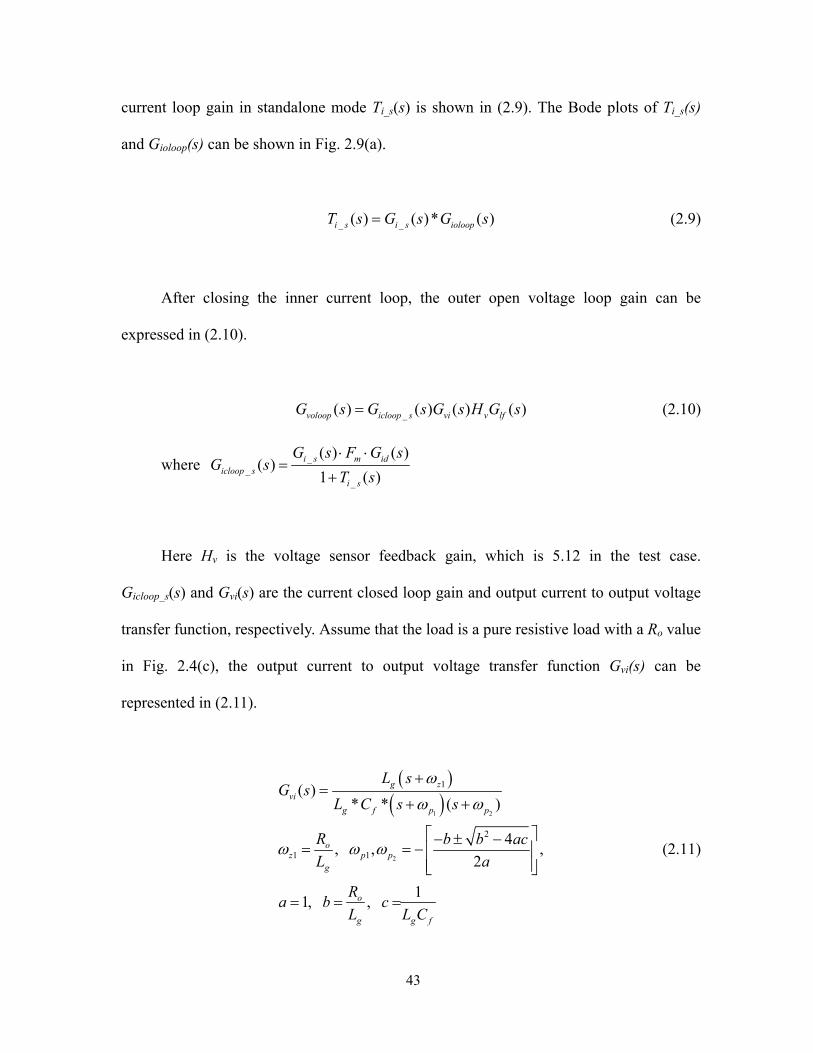
After closing the inner current loop, the outer open voltage loop gain can be
expressed in (2.10).
_( ) ( ) ( ) ( )voloop icloop s vi v lfG s G s G s H G s= (2.10)
where __
_
( ) ( )( )
1 ( )i s m id
icloop si s
G s F G sG s
T s⋅ ⋅
=+
Here Hv is the voltage sensor feedback gain, which is 5.12 in the test case.
Gicloop_s(s) and Gvi(s) are the current closed loop gain and output current to output voltage
transfer function, respectively. Assume that the load is a pure resistive load with a Ro value
in Fig. 2.4(c), the output current to output voltage transfer function Gvi(s) can be
represented in (2.11).
( )( )1 2
2
1
2
1 1
( )* * ( )
4, , ,2
11, ,
g zvi
g f p p
oz p p
g
o
g g f
L sG s
L C s s
R b b acL a
Ra b cL L C
ω
ω ω
ω ω ω
+=
+ +
⎡ ⎤− ± −= = − ⎢ ⎥
⎢ ⎥⎣ ⎦
= = =
(2.11)

44
The design goal of a dual-loop voltage controller is to obtain a high gain at the
fundamental frequency while providing enough bandwidth and stability margin. As shown
in (2.12), a PR controller is adopted here to eliminate the steady-state error by providing a
high gain at the fundamental frequency.
2 21
2( )2
c rv p
c
k sG s ks s
ωω ω
= ++ +
(2.12)
With 20% load as the design plant, a PR controller is designed to have kp = 0.02, kr
= 12, ωc = 10 rad/s, and ω1 = 377 rad/s. The resulting Bode plots of the compensated
voltage loop gain Tv(s) = Gv(s) ⋅Gvoloop(s) along with the uncompensated voltage loop gain
Gvoloop(s) are shown in Fig. 2.9(b).
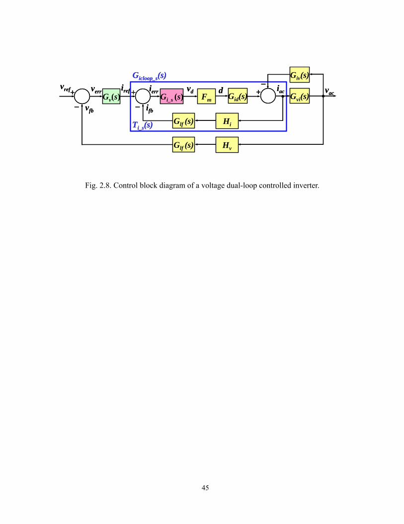
45
iref
ifb
vdierr
_+ FmGi_s (s)
iacdGid(s) Gvi(s)
vacvref
vfb
verr
_+ Gv(s)
Glf (s) Hi
Glf (s) Hv
Ti_s(s)
+–
Giv(s)Gicloop_s(s)iref
ifb
vdierr
_+ FmGi_s (s)
iacdGid(s) Gvi(s)
vacvref
vfb
verr
_+ Gv(s)
Glf (s) Hi
Glf (s) Hv
Ti_s(s)
+–
Giv(s)Gicloop_s(s)
Fig. 2.8. Control block diagram of a voltage dual-loop controlled inverter.
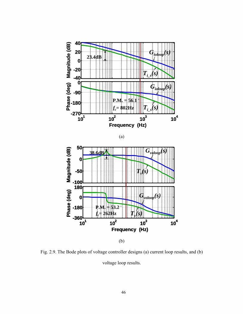
46
101 102 103 104-270
-180
-90
0
Phas
e (d
eg)
-40-20
0
20
40
Mag
nitu
de (d
B)
Frequency (Hz)
23.4dB
Ti_s(s)
Gioloop(s)
Ti_s(s)
Gioloop(s)
fc= 802HzP.M. = 56.1。
101 102 103 104-270
-180
-90
0
Phas
e (d
eg)
-40-20
0
20
40
Mag
nitu
de (d
B)
Frequency (Hz)
23.4dB
Ti_s(s)
Gioloop(s)
Ti_s(s)
Gioloop(s)
fc= 802HzP.M. = 56.1。
(a)
-100
-50
0
50
Mag
nitu
de (d
B)
101 102 103 104-360
-180
0
180
Phas
e (d
eg)
Frequency (Hz)
38.6dB
Tv(s)
Gvoloop(s)
Tv(s)
Gvoloop(s)
fc= 262HzP.M. = 53.2。
-100
-50
0
50
Mag
nitu
de (d
B)
101 102 103 104-360
-180
0
180
Phas
e (d
eg)
Frequency (Hz)
-100
-50
0
50
Mag
nitu
de (d
B)
101 102 103 104-360
-180
0
180
Phas
e (d
eg)
Frequency (Hz)
38.6dB
Tv(s)
Gvoloop(s)
Tv(s)
Gvoloop(s)
fc= 262HzP.M. = 53.2。
(b)
Fig. 2.9. The Bode plots of voltage controller designs (a) current loop results, and (b)
voltage loop results.
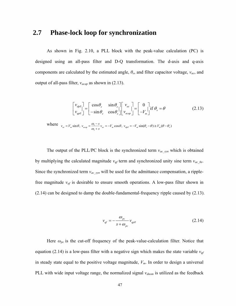
47
2.7 Phase-lock loop for synchronization
As shown in Fig. 2.10, a PLL block with the peak-value calculation (PC) is
designed using an all-pass filter and D-Q transformation. The d-axis and q-axis
components are calculated by the estimated angle, θe, and filter capacitor voltage, vac, and
output of all-pass filter, vacap as shown in (2.13).
cos sin 0
if sin cos
dpll ace ee
qpll acape e m
v vv v V
θ θθ θ
θ θ⎡ ⎤ ⎡ ⎤⎡ ⎤ ⎡ ⎤
= = =⎢ ⎥ ⎢ ⎥⎢ ⎥ ⎢ ⎥− −⎣ ⎦ ⎣ ⎦⎣ ⎦ ⎣ ⎦ (2.13)
where 1
1
sin , cos , sin( ) ( )ac m acap ac m dpll m e m esv V v v V v V Vs
ωθ θ θ θ θ θω
−= = = − = − − ≅ −
+
The output of the PLL/PC block is the synchronized term vac_syn which is obtained
by multiplying the calculated magnitude vqf term and synchronized unity sine term vac_θe.
Since the synchronized term vac_syn will be used for the admittance compensation, a ripple-
free magnitude vaf is desirable to ensure smooth operations. A low-pass filter shown in
(2.14) can be designed to damp the double-fundamental-frequency ripple caused by (2.13).
pcqf qpll
pc
v vsωω
= −+
(2.14)
Here ωpc is the cut-off frequency of the peak-value-calculation filter. Notice that
equation (2.14) is a low-pass filter with a negative sign which makes the state variable vqf
in steady state equal to the positive voltage magnitude, Vm. In order to design a universal
PLL with wide input voltage range, the normalized signal vdnom is utilized as the feedback
48
signal for the PLL. With an integrator as the PLL plant Gpll(s), a controller Gcpll(s) is
designed to have a compensated loop gain Tpll(s) with a 28-Hz cross-over frequency and a
36o phase margin as shown in (2.15) and Fig. 2.10(b).
( ) ( )pll cpll PLLT G s G s= (2.15)
where 1( ) , ( ) p llp ll cp ll p ll
p ll
G s G s ks s
ωω
= =+
Here ωpll, kpll are the cut-off frequency and gain of the PLL controller. As can be
seen from the Fig. 2.10(b), the compensated PLL loop gain Tpll(s) has a very high gain at
zero Hz. This high loop gain means that the input signal vdnom will eventually converge to
zero and make the output estimated angle eθ follow the input angle θ as shown in
(2.16).
sin( ) 0 if d m ednom e e
qf m
v Vvv V
θ θ θ θ θ θ−= = = − = ≅ (2.16)
49
D-QTransformation
vac
Gap(s)Gfpc(s)
vacap
vdpll
vqpll vqf
Gcpll(s) ++
++∫
vdnom
00 __
++
vdnom
sinvac_θe vac_synωe
ω1
ωdif θe
D-QTransformation
vac
Gap(s)Gfpc(s)
vacap
vdpll
vqpll vqf
Gcpll(s) ++
++∫
vdnom
00 __
++
vdnom
sinvac_θe vac_synωe
ω1
ωdif θe
(a)
-100
-50
0
50
Mag
nitu
de (d
B)
100 101 102 103-180
-135
-90
-45
Phas
e (d
eg)
Bode Diagram
Frequency (Hz)
Tpll(s)Gpll(s)
fc= 28HzP.M. = 36。
Tpll(s)Gpll(s)
-100
-50
0
50
Mag
nitu
de (d
B)
100 101 102 103-180
-135
-90
-45
Phas
e (d
eg)
Bode Diagram
Frequency (Hz)
Tpll(s)Gpll(s)
fc= 28HzP.M. = 36。
Tpll(s)Gpll(s)
(b)
Fig. 2.10. Phase-lock loop with the peak-value calculation (a) control block diagram, and
(b) PLL loop plot showing crossover frequency of 28Hz and phase margin of 36°.

50
2.8 Simulation and experimental verification
Fig. 2.11 shows the simulation results of the phase-lock loop and peak-value
calculation. As can be seen from the top figure, the output signal vac_syn can track the input
signal vac in both the phase and magnitude after a few fundamental cycles. The middle and
bottom figures show the output of all-pass filter vacap and the peak-value calculation output
vqf. The simulation results show that the designed PLL controller and peak-value
calculation works properly.
A PCS prototype that contains a dc-dc converter to boost the fuel cell voltage from
about 25V to 400V and a dc-ac inverter that produces 208V ac output for the grid
connection is tested with a solid oxide fuel cell (SOFC) simulator, which mimics an actual
low-voltage SOFC that has a stack of 36 cells operating at 1000°C. Fig. 2.12 shows test
setup with the PCS prototype and associated instrumentation. A precision current shunt is
used to calibrate the current measurement. The front panel of the case is open to show the
DSP board.

51
0
-50
-100
50
100
Vac Vac_syn
0
-50
-100
-150
50
100
Vaccap Vac
0 0.02 0.04 0.06 0.08 0.1 0.12 0.14 0.16 0.18 0.2Time (s)
0
-20
20
40
60
80
100
Vqf
vac vac_syn
vac vacap
vqf
40V
50V
50V 0
-50
-100
50
100
Vac Vac_syn
0
-50
-100
-150
50
100
Vaccap Vac
0 0.02 0.04 0.06 0.08 0.1 0.12 0.14 0.16 0.18 0.2Time (s)
0
-20
20
40
60
80
100
Vqf
vac vac_syn
vac vacap
vqf
40V
50V
50V
Fig. 2.11. Simulation results of phase-lock loop and peak value calculation.
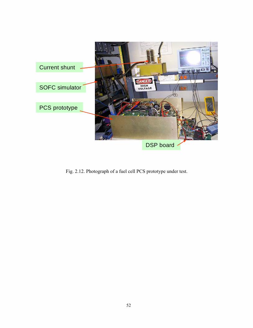
52
SOFC simulator
Current shunt
PCS prototype
DSP board
Fig. 2.12. Photograph of a fuel cell PCS prototype under test.
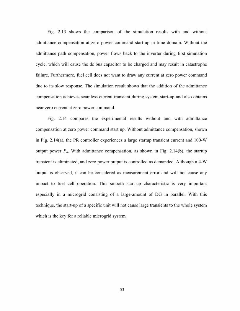
53
Fig. 2.13 shows the comparison of the simulation results with and without
admittance compensation at zero power command start-up in time domain. Without the
admittance path compensation, power flows back to the inverter during first simulation
cycle, which will cause the dc bus capacitor to be charged and may result in catastrophe
failure. Furthermore, fuel cell does not want to draw any current at zero power command
due to its slow response. The simulation result shows that the addition of the admittance
compensation achieves seamless current transient during system start-up and also obtains
near zero current at zero power command.
Fig. 2.14 compares the experimental results without and with admittance
compensation at zero power command start up. Without admittance compensation, shown
in Fig. 2.14(a), the PR controller experiences a large startup transient current and 100-W
output power Po. With admittance compensation, as shown in Fig. 2.14(b), the startup
transient is eliminated, and zero power output is controlled as demanded. Although a 4-W
output is observed, it can be considered as measurement error and will not cause any
impact to fuel cell operation. This smooth start-up characteristic is very important
especially in a microgrid consisting of a large-amount of DG in parallel. With this
technique, the start-up of a specific unit will not cause large transients to the whole system
which is the key for a reliable microgrid system.
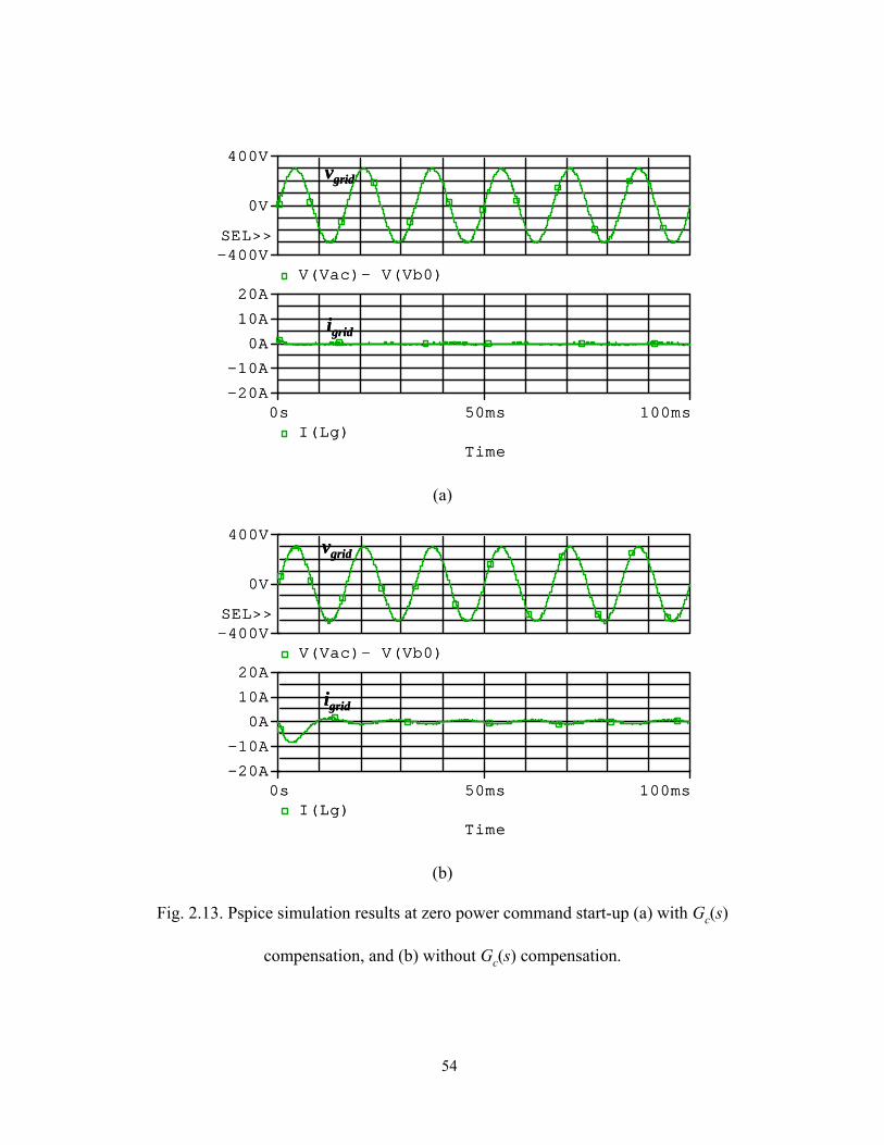
54
vgrid
igrid
Time
0s 50ms 100msI(Lg)
-20A
-10A
0A
10A
20AV(Vac)- V(Vb0)
-400V
0V
400V
SEL>>
vgrid
igrid
Time
0s 50ms 100msI(Lg)
-20A
-10A
0A
10A
20AV(Vac)- V(Vb0)
-400V
0V
400V
SEL>>
(a)
Time
0s 50ms 100msI(Lg)
-20A
-10A
0A
10A
20AV(Vac)- V(Vb0)
-400V
0V
400V
SEL>>
vgrid
igrid
Time
0s 50ms 100msI(Lg)
-20A
-10A
0A
10A
20AV(Vac)- V(Vb0)
-400V
0V
400V
SEL>>
vgrid
igrid
(b)
Fig. 2.13. Pspice simulation results at zero power command start-up (a) with Gc(s)
compensation, and (b) without Gc(s) compensation.
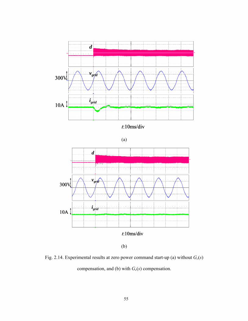
55
t:10ms/div
300Vvgrid
d
10Aigrid
t:10ms/div
300Vvgrid
d
10Aigrid
(a)
10Aigrid
300Vvgrid
d
t:10ms/div
10Aigrid
300Vvgrid
d
t:10ms/div
(b)
Fig. 2.14. Experimental results at zero power command start-up (a) without Gc(s)
compensation, and (b) with Gc(s) compensation.

56
Fig. 2.15(a) shows the simulation results of the LCL-filter inverter running in
current-mode control with PR controller and admittance compensation. The results show
that the output current follows a 32-A peak command current very well because of a high
loop gain at the fundamental frequency.
Fig. 2.15(b) shows the experimental results under 32-A peak current command in
the grid-tie condition. Waveforms indicate that the output current follows the command
well. Both the simulation and experimental results validate the effectiveness of the
designed controller.
Fig. 2.16(a) and Fig. 2.16(b) show the simulation and experimental results of the
dual-loop controlled LCL-filter inverter with a PR-controller based outer voltage-loop and
a P-controller based inner current-loop operation. The output voltage vac is 215 V rms, and
the output current iload is 24.2 A rms. The power output of 5.2-kW goes into a pure
resistive load in both simulated and tested cases. The simulation includes all the dynamics
of system transfer function and controller blocks shown in Fig. 2.8. Again, the simulation
result and experimental results shows that designed controller is capable to obtain stable
outputs with precise power control.

57
Time
100ms 150ms 200msI(Lg)
-40A
0A
40A
SEL>>
V(Vac)- V(Vb0)-400V
0V
400V
vac
igrid
Time
100ms 150ms 200msI(Lg)
-40A
0A
40A
SEL>>
V(Vac)- V(Vb0)-400V
0V
400V
vac
igrid
(a)
t:10ms/div
20A
300Vvac
igrid
t:10ms/div
20A
300Vvac
igrid
(b)
Fig. 2.15. Current loop implementation results at 4.85kW (a) Pspice simulation result at
32A iref, pk, , and (b) experimental result at 32A iref, pk.
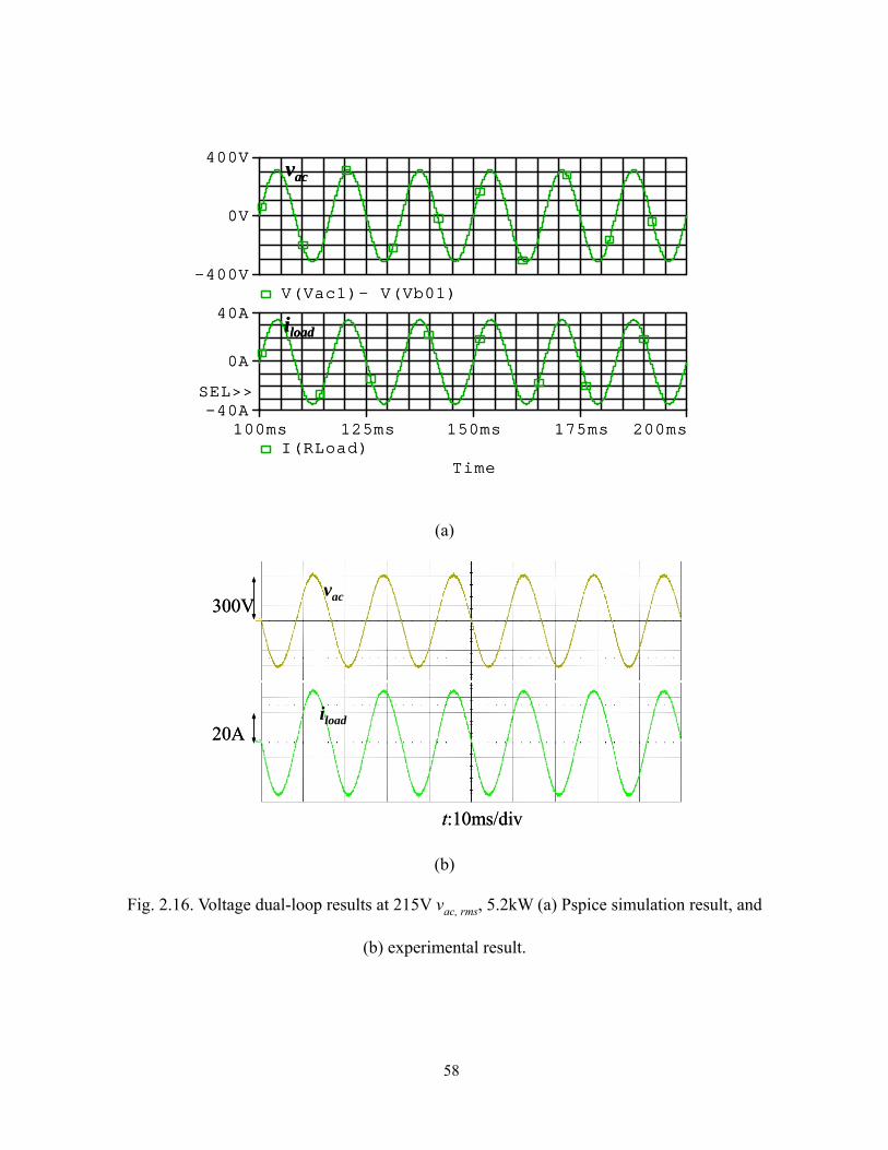
58
Time
100ms 125ms 150ms 175ms 200msI(RLoad)
-40A
0A
40A
SEL>>
V(Vac1)- V(Vb01)-400V
0V
400Vvac
iload
Time
100ms 125ms 150ms 175ms 200msI(RLoad)
-40A
0A
40A
SEL>>
V(Vac1)- V(Vb01)-400V
0V
400Vvac
iload
(a)
t:10ms/div
300V
20A
vac
iload
t:10ms/div
300V
20A
vac
iload
(b)
Fig. 2.16. Voltage dual-loop results at 215V vac, rms, 5.2kW (a) Pspice simulation result, and
(b) experimental result.

59
2.9 Summary
Complete design and implementation results of a single-phase universal power
conditioning system operating in both grid-tie and standalone modes were presented in
this chapter. Key design features of the proposed inverter system are summarized as
follows.
1. Admittance compensation
The proposed admittance compensation not only also allows the grid-tie system to
be controlled like a first-order system but also helps reduce the start-up transient
during the grid-tie connection to improve system reliability by preventing the reverse
power flow.
2. Design of LCL filter
This chapter suggests several design considerations based on the current ripple,
stability, output performance, sensor location, noise concern, and the ease of controller
design.
3. Design of dual- and single-loop controllers
For the grid-tie operation, a single current loop controller design with PR controller
and admittance compensation is proposed to reduce the steady-state error while
maintaining system stability. For the standalone operation, a dual-loop control system
with PR-controller for outer voltage loop and a P-controlled for inner current loop is
proposed to limit peak current magnitude under transient, enhance voltage loop
stability, and reduce voltage steady-state error.
60
4. Design of phase-lock loop
The PLL provides the synchronized phase of the current command which is the key
for precision power flow control. The band-pass-filter feature of PLL also allows the
input of the admittance compensation to avoid the dc offset and high-frequency noise
in the feedback network.
The proposed admittance compensation and current loop controller has been
simulated and implemented in a DSP-based 5-kW PCS. Without admittance compensation,
both simulation and experiment results show that a significant startup transient and non-
zero current output at zero power command. The power flow in the first cycle is reversed,
and the energy is erratically fed back to the inverter, which may cause over voltage in the
dc link and result in catastrophic failure. With admittance compensation, a smooth startup
was observed in both simulation and experiment. The zero current command can be
precisely achieved.
Simulation and experimental results show that the designed inverters are capable of
operating in both grid-tie and standalone modes by adapting to different controller sets
with the same hardware setup. The LCL filter based inverter controlled with the proposed
single- and dual-loop controllers for different operating modes shows stable output
waveforms. These results validate that the proposed universal-inverter with LCL filter, the
dual-loop voltage and single-loop current controllers can be as the key elements for
microgrid applications where both the grid-tie and standalone operations are required.

61
Chapter 3
Current Sharing and Smooth Mode Transfer of Parallel Inverters in Microgrid Applications
3.1 Introduction
In this chapter, the inverter control in previous chapter is utilized as the building
block for a small-scale microgrid system with multiple inverter-based DGs. Two main
issues will be discussed: (1) current-sharing in the islanding mode of a microgrid, and (2)
smooth mode transfers between the islanding mode and grid-tie mode.
In order to minimize the system thermal stress or perform the power management to
achieve system cost effectively, the microgrid system should perform the current sharing
among the paralleled inverters through the communication channels. In this chapter, a
frequency-decoupled command transmission method was proposed so that it can transmit
in a longer distance with a low bandwidth communication channel.

62
For the microgrid system, the designed system should be able to smoothly transfer
between two basic operation modes and continuously supply the critical loads. In order to
minimize the excessive electrical stresses, the considerations for a seamless transfer are
provided and proper mode transfer procedures are suggested.
63
3.2 Basic microgrid operations with LCL parallel inverters
In a microgrid system, there are two basic operation modes: grid-tie mode and
islanding mode. Fig. 3.1 shows the hardware configuration of the parallel-inverter
microgrid system running in the islanding mode. If the grid is not available, the SSR is
disconnected and the system supplies its own power to the critical load. In chapter 2,
standalone mode stands for a single inverter running in the dual voltage loop. The
islanding mode here refers to a cluster of parallel inverters operating together to supply the
critical load. One of the inverters has to operate in the voltage dual-loop control and serve
as a voltage source, while the rest of the inverters operate in the single current-loop
control to share the current as required. When the grid recovers, the SSR is reconnected
and all the inverters in the system run in the single current mode to supply energy to the
critical load and to exchange energy with the grid.
Fig. 3.2 shows the control block diagram of the parallel-inverter microgrid system
running in the islanding mode. Every individual inverter has its own DSP controller and
there is an upper-level controller which provides the mode attribute and the mode-transfer
command generation for the inverters in the system. When the microgrid system in Fig.
3.1 switches from the islanding mode to grid-tie mode, only the control of the first inverter
changes from the voltage-control mode to current-control mode as shown in Fig. 3.3;
while the control of the other inverters stays the same. At least one inverter is operating in
the voltage dual-loop control in the islanding mode. Conversely, all inverters are running
in the current single-loop control in the grid-tie mode. The selection of the inverter

64
running in the voltage-mode or current-mode control is also determined by the upper-level
controller through the CAN bus.
With the hot-swap CAN bus, the communication channel will still survive even
when one single node is disconnected. In addition, when the original dual-loop unit fails,
the microgrid system still can function because the upper-level controller will assign
another inverter as the dual-loop control and keep the whole system running. However, the
CAN bus or upper-level controller may fail. In this case, it is necessary to adopt other
backup control methods such as droop control [24], [50]-[53] or circular-chain control [25]
to improve system reliability. These added backup control methods may increase the
hardware cost due to increased communication ports or the software burden due to
additional computation requirement.

65
Liiac1 iout1Lg
vac1Cf vbusvi1
Rload
iloadinverter
1
Liiac2 iout2Lg
vac2Cf vbusvi2inverter
2
Liiacn ioutnLg
vacnCf vbusvininverter
n
dc-dcconverter
Vin-1 Vdc1
dc-dcconverterVin-2 Vdc2
dc-dcconverterVin-n Vdcn
Grid
SSR
~
igrid
vgrid+
-
Ls
Upper-level controller
Liiac1 iout1Lg
vac1Cf vbusvi1
Rload
iloadinverter
1
Liiac2 iout2Lg
vac2Cf vbusvi2inverter
2
Liiacn ioutnLg
vacnCf vbusvininverter
n
dc-dcconverter
Vin-1 Vdc1
dc-dcconverterVin-2 Vdc2
dc-dcconverterVin-n Vdcn
Grid
SSR
~~
igrid
vgrid+
-
Ls
Upper-level controller
Fig. 3.1. The hardware configuration of parallel-inverter microgird system.
66
iifb1fb1
vvd1d1iierr1err1
__++ FFmmGGii __ss((ss))
iiac1ac1dd11 GGidid(s(s)) GGvivi(s(s))vvac1ac1
GGlflf (s)(s) HHiiTTi_si_s(s(s))
++––
GGiviv(s(s))GGicloop_sicloop_s(s(s))
iiref2 ref2
iifb2fb2
vvd2d2iierr2err2
__++ FFmmGGi_gi_g ((ss))
iiac2ac2dd22 GGidid(s(s)) GGvivi(s(s))vvac2ac2
GGlflf (s)(s) HHiiTTi_gi_g(s(s))
++––
GGiviv(s(s))GGicloop_gicloop_g(s(s))
Inverter 1Inverter 1-- Voltage ControlVoltage Control
PLLPLL
PLLPLL
CAN T/RCAN T/R
Inverter 2Inverter 2-- Current ControlCurrent Control
Inverter nInverter n-- Current ControlCurrent Control
CAN CAN BusBus
MA & CG: Mode arbitration and command generationMA & CG: Mode arbitration and command generationPC: Peak value calculation, ARG: Automatic reference generationPC: Peak value calculation, ARG: Automatic reference generation
PCPCiiac1_pkac1_pkCAN T/RCAN T/R
PCPCARGARGiiac1_pkac1_pk iiac2_pkac2_pk
iiac2_ac2_θθee
vvac2_ac2_θθee
GGlflf (s)(s) HHii
CAN T/RCAN T/Riigrid_fbgrid_fb
iigridgrid
UpCmdUpCmd
UpCmdUpCmd
UpperUpper--Level ControllerLevel Controller
iirefref 1 1 vvrefref 1 1
vvfb1fb1
vverr1err1__
++ GGvv((ss))
GGlflf (s)(s) HHvv
UpCmdUpCmd
GGlflf (s)(s) HHvvvvgrid_fbgrid_fb
vvgridgrid
GGlflf (s)(s) HHvvvvbus_fbbus_fb
vvbusbusiigrid_pkgrid_pk
iigrid_pkgrid_pk
iigrid_pkgrid_pk
vvgrid_pkgrid_pkvvgrid_grid_θθee
vvgrid_grid_θθee
vvgrid_pkgrid_pk
MAMA&&
CGCG
Fig. 3.2. Control block diagrams of the parallel-inverter microgrid system in islanding
mode.
67
iifb1fb1
vvd1d1iierr1err1
__++ FFmmGGii __gg((ss))
iiac1ac1dd11 GGidid(s(s)) GGvivi(s(s))vvac1ac1
GGlflf (s)(s) HHiiTTi_gi_g(s(s))
++––
GGiviv(s(s))GGicloop_gicloop_g(s(s))
iiref2 ref2
iifb2fb2
vvd2d2iierr2err2
__++ FFmmGGi_gi_g ((ss))
iiac2ac2dd22 GGidid(s(s)) GGvivi(s(s))vvac2ac2
GGlflf (s)(s) HHiiTTi_gi_g(s(s))
++––
GGiviv(s(s))GGicloop_gicloop_g(s(s))
Inverter 1Inverter 1-- Current ControlCurrent Control
PLLPLL
PLLPLL
CAN T/RCAN T/R
Inverter 2Inverter 2-- Current ControlCurrent Control
Inverter nInverter n-- Current ControlCurrent Control
CAN CAN BusBus
MA & CG: Mode arbitration and command generationMA & CG: Mode arbitration and command generationPC: Peak value calculation, ARG: Automatic reference generationPC: Peak value calculation, ARG: Automatic reference generation
PCPCiiac1_pkac1_pkCAN T/RCAN T/R
PCPCARGARGiiac1_pkac1_pk iiac2_pkac2_pk
iiac2_ac2_θθee
vvac2_ac2_θθee
GGlflf (s)(s) HHii
CAN T/RCAN T/Riigrid_fbgrid_fb
iigridgrid
UpCmdUpCmd
UpCmdUpCmd
UpperUpper--Level ControllerLevel Controller
iirefref 1 1
UpCmdUpCmd
GGlflf (s)(s) HHvvvvgrid_fbgrid_fb
vvgridgrid
GGlflf (s)(s) HHvvvvbus_fbbus_fb
vvbusbusiigrid_pkgrid_pk
iigrid_pkgrid_pk
iigrid_pkgrid_pk
vvgrid_pkgrid_pkvvgrid_grid_θθ
vvgrid_grid_θθee
vvgrid_pkgrid_pk
MAMA&&
CGCG
PLLPLLvvac1_ac1_θθee
iirefref 1_pk1_pk
Fig. 3.3. Control block diagrams of the parallel-inverter microgrid system in grid-tie mode.

68
3.3 Current sharing and synchronization through CAN bus
The current sharing capability is important for a reliability and/or cost effectively
system. As shown in Fig. 3.2, the microgrid can share the currents among parallel
inverters by the peak value calculation (PC), the automatic reference generation (ARG),
and the phase-lock loop (PLL) blocks through the CAN bus. As shown in (3.1), once the
PC and the PLL detect the magnitude and phase information, the ARG adjusts the current
reference iref2 so that the current peak difference and phase difference are minimized.
2 2_ 2 _*ref ref pk refi i i θ= (3.1)
where _ _ 1_ 2_ _
2_ 1_ _
_ _ _ 1_ 2 _ _
if ,
if
pk offset pk offset ac pk ac pk pk band
ref pk ac pk pk offset
pk offset pk offset pk step ac pk ac pk pk band
i i i i ii i i
i i i i i i
⎧ = − <⎪= + ⎨= ± − >⎪⎩
_ _ 2_ 2_ _
2_ 2_ _
_ _ _ 2 _ 2_ _
if ,
if
offset offset ac e ac e band
ref ac e offset
offset offset step ac e ac e band
i i v i ii v i
i i i v i i
θ θ θ θ θ
θ θ θ
θ θ θ θ θ θ
⎧ = − <⎪= + ⎨= ± − >⎪⎩
Here the ipk_band and iθ_band are the magnitude and phase bands for the inequality
condition. The ipk_step and iθ_step are the magnitude and phase step sizes respectively to
modify the magnitude offset ipk_offset and the phase offset iθ_offset. In this system, only the
digitally formatted ac signal magnitude and phase information need to be transmitted. The
frequency information does not need to be transmitted because it will be automatically
tracked by the PLL.

69
Without transmitting the actual 50 or 60Hz ac signal, the transmitting bandwidth
can be lowered and the transmission distance can be largely extended. For frequency-
decoupled signal transmission, the signal transmitted is the current reference signal which
requires a maximum 1kHz bandwidth due to the inner current loop with a 1.45kHz cross-
over frequency. However, if the 60Hz signal is transmitted in ac form which frequency
and magnitude are both transmitted, then a 1kHz bandwidth communication channel will
cause a 21.6 degree phase delay. This means that the output currents of two parallel
inverters will have at least 21.6 degree difference even if the current loop bandwidth is
infinite. In order to reduce this current reference phase delay to less than one degree for
60Hz ac signal transmission, the communication channel needs to have a bandwidth at
22kHz or more. Table 3.1 shows the relationship between maximum signaling rate and
cable length of CAN bus [97]. Assume the data length per transmission of both ac and
frequency-decoupled signal transmission are the same, this table indicates that the bus
length of the frequency decoupled method can be 30 times longer of if the signaling rate is
20 times less.
Thanks to the differential transmission and the CAN bus error checking protocol,
the signal transmission can be very reliable even in a noisy environment [98]. The CAN
protocol incorporates five methods of error checking: monitoring checks, cyclic
redundancy check, bit stuffing, and message frame check. A very tiny message error rate
of undetected error at 4.7 * 10-11 can be achieved by these well designed error-detection
mechanism. For a message error rate of 100/sec, there will be 1 undetected error per 2,462
days operation.

70
Table 3.1 Maximum signal rates for various cable lengths of CAN bus
Bus length (m) Signaling rate (kbps)
30 1000
100 500
250 250
500 125
1000 62.5

71
3.4 Mode transfer considerations Performance evaluation of generalized control structure
As shown in Fig. 3.1, the parallel-inverter microgrid system should either supply the
critical load Rload and exchange the power with the grid when the grid is available, or keep
supplying the Rload when the grid is not available. In order to keep supplying power to
Rload, the microgrid system is required to switch between grid-tie and islanding modes
without drastic electrical stresses. If the system does not have the proper mode transfer
procedure, severe transient voltages or currents will occur which may damage the entire
system. Since the whole microgrid is controlled like a current source in the grid-tie mode
and a voltage-controlled output in islanding mode, the key of a smooth transfer is to
comply with the basic circuit laws: (i) do not interrupt a large magnitude of current on the
switch, (ii) do not connect two voltage sources directly without well matched and
synchronized magnitude, frequency and phase.
With the control block diagram shown in Fig. 3.3, the proposed procedure to change
from the grid-tie to islanding mode is summarized as:
(a) The upper-level controller detects the fault on the grid vgrid and extracts the grid
current information igrid.
(b) Through the CAN bus, the upper-level controller provides igrid information and
commands all the current-controlled inverters to change their outputs, so that the
current on the SSR igrid can be minimized to avoid mode transfer transient.

72
(c) The upper-level controller provides the turn-off signal for the SSR after a certain
waiting time, for example, 5 cycles.
(d) Through the CAN bus, the upper-level controller commands a selected inverter
(inverter 1) to change from the current-controlled mode to voltage-controlled mode
at the next zero crossing.
(e) Inverter 1 regulates the bus voltage to a desired level and provides the output
current information to inverter 2, so that they can share the total current in the
islanding mode.
Since the inverter-based microgrid tends to have small over-current capability, the
5-cycle waiting is chosen to ensure smooth current transfer while considering the 10-cycle
clearing time under the worse case abnormal grid voltage and frequency conditions [20].
However, this waiting time can be set to another value to accommodate equipment
electrical ratings and a desirable clearing time in different fault conditions. On the other
hand, the procedure to change from the islanding to grid-tie mode is summarized as:
(a) The upper-level controller detects if the grid voltage vgrid recovers and keeps
detecting the grid voltage magnitude vgrid_pk and phase vgrid_θe information.
(b) Through the CAN bus, the upper-level controller provides the grid voltage
information and commands the inverter 1 to adjust vbus to track vgrid in both
magnitude and phase.
(c) The upper-level controller keeps monitoring vbus and vgrid. It turns on the SSR once
the two voltages are synchronized in phase and magnitude.

73
(d) Through the CAN bus, the upper-level controller commands the inverter 1 to
change its controller from the voltage-controlled mode to current-controlled mode
at the next zero-crossing. It assigns the current references so that zero current goes
through the SSR during the transfer transient.
(e) The current controlled inverters change the current reference to a desired level.
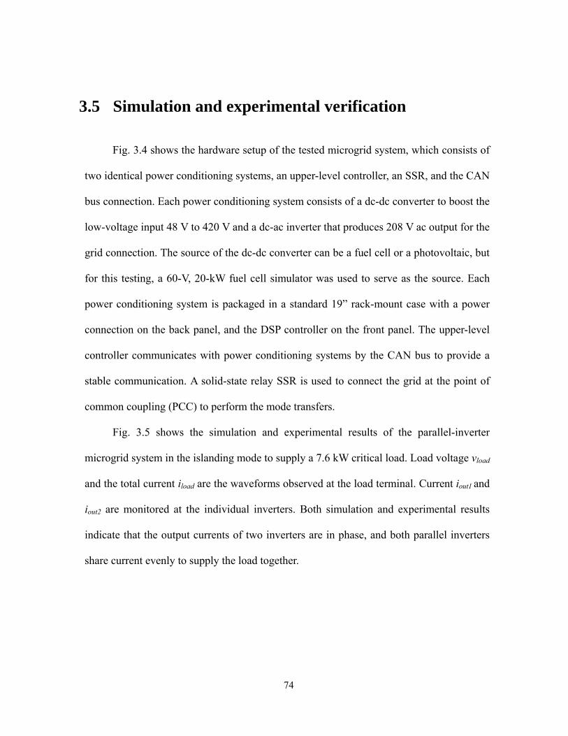
74
3.5 Simulation and experimental verification
Fig. 3.4 shows the hardware setup of the tested microgrid system, which consists of
two identical power conditioning systems, an upper-level controller, an SSR, and the CAN
bus connection. Each power conditioning system consists of a dc-dc converter to boost the
low-voltage input 48 V to 420 V and a dc-ac inverter that produces 208 V ac output for the
grid connection. The source of the dc-dc converter can be a fuel cell or a photovoltaic, but
for this testing, a 60-V, 20-kW fuel cell simulator was used to serve as the source. Each
power conditioning system is packaged in a standard 19” rack-mount case with a power
connection on the back panel, and the DSP controller on the front panel. The upper-level
controller communicates with power conditioning systems by the CAN bus to provide a
stable communication. A solid-state relay SSR is used to connect the grid at the point of
common coupling (PCC) to perform the mode transfers.
Fig. 3.5 shows the simulation and experimental results of the parallel-inverter
microgrid system in the islanding mode to supply a 7.6 kW critical load. Load voltage vload
and the total current iload are the waveforms observed at the load terminal. Current iout1 and
iout2 are monitored at the individual inverters. Both simulation and experimental results
indicate that the output currents of two inverters are in phase, and both parallel inverters
share current evenly to supply the load together.

75
With the observation of the total current iload being equal to the sum of iout1 and iout2,
one can easily conclude that there is no observable circulating current between the dual-
loop controlled and single-loop controlled inverters. The even current distribution
suggests that the microgrid system along with CAN communication, phase-locked loop
and automatic phase adjustment control works effectively.

76
upper-level controller
SSRPCS-1 PCS-2
CAN Bus
dc-ac-inverter
dc-dc-converter
DSP controller
upper-level controller
SSRPCS-1 PCS-2
CAN Bus
dc-ac-inverter
dc-dc-converter
DSP controller
Fig. 3.4. Photograph of the proposed microgrid system.
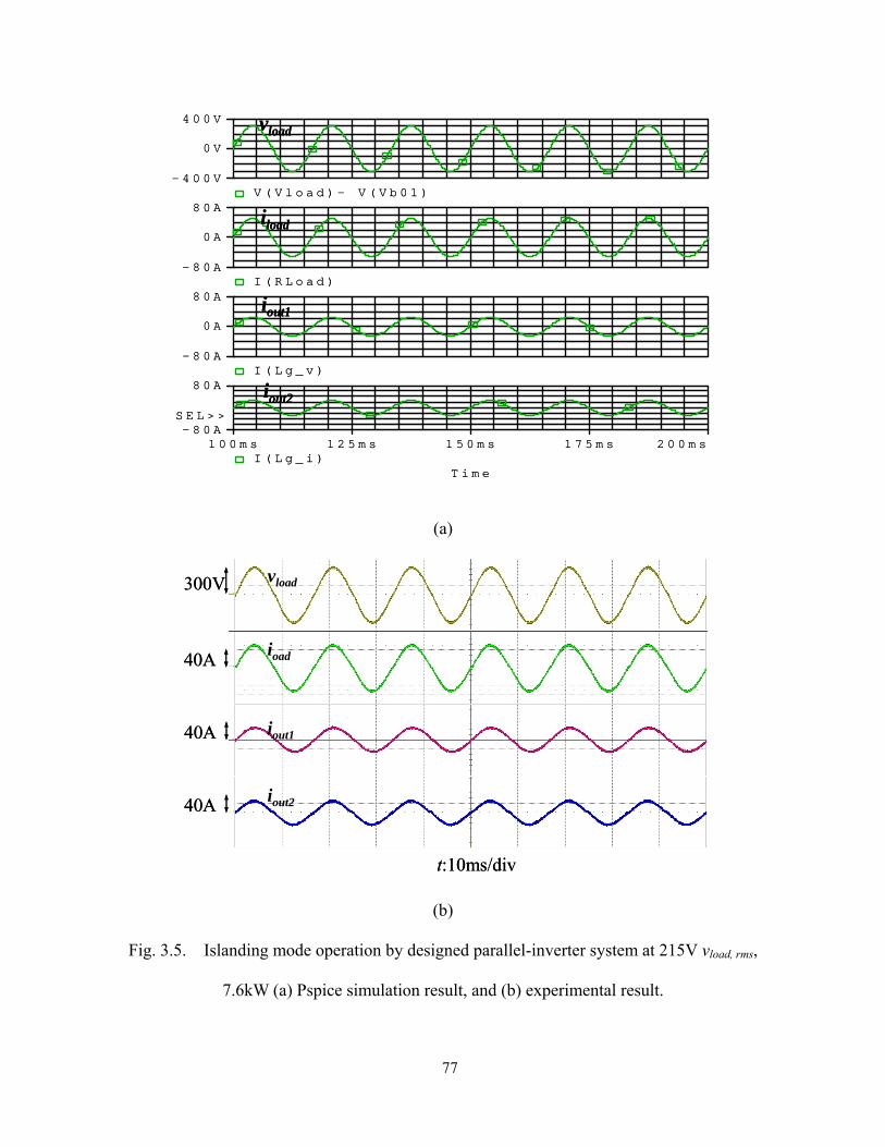
77
T i m e
1 0 0 m s 1 2 5 m s 1 5 0 m s 1 7 5 m s 2 0 0 m sI ( L g _ i )
- 8 0 A
8 0 A
S E L > >
I ( L g _ v )- 8 0 A
0 A
8 0 AI ( R L o a d )
- 8 0 A
0 A
8 0 AV ( V l o a d ) - V ( V b 0 1 )
- 4 0 0 V
0 V
4 0 0 V vload
iload
iout1
iout2
T i m e
1 0 0 m s 1 2 5 m s 1 5 0 m s 1 7 5 m s 2 0 0 m sI ( L g _ i )
- 8 0 A
8 0 A
S E L > >
I ( L g _ v )- 8 0 A
0 A
8 0 AI ( R L o a d )
- 8 0 A
0 A
8 0 AV ( V l o a d ) - V ( V b 0 1 )
- 4 0 0 V
0 V
4 0 0 V vload
iload
iout1
iout2
(a)
vload
ioad
iout1
t:10ms/div
40A iout2
40A
40A
300V vload
ioad
iout1
t:10ms/div
40A iout2
40A
40A
300V
(b)
Fig. 3.5. Islanding mode operation by designed parallel-inverter system at 215V vload, rms,
7.6kW (a) Pspice simulation result, and (b) experimental result.

78
Fig. 3.6 and Fig. 3.7 show the simulation and experimental results of the mode
transfer from the grid-tie mode to islanding mode for the parallel-inverter microgrid
system. For the mode transfer tests, the grid voltage is simulated by an additional voltage-
controlled inverter so that the simulated grid voltage can be regulated to trigger the mode
transfer. For the safety considerations, the mode transfers are conducted with the
following resistors to limit the transient currents: a 2.5-Ω resistor in series with the
simulated grid, a 1.6-Ω resistor in series with the inverter 1 output, and a 1-Ω resistor in
series with the output of inverter 2. Before the mode transfer, all the inverters in the
microgrid system operate in the grid-tie mode so that the bus voltage vbus is the same as
the grid voltage vgrid. Notice that the igrid and vgrid are 180 degrees out of phase which
means that the grid also supplies power to the critical load Rload before the mode transfer.
Once the grid voltage vgrid is higher than a preset limit (135V rms), the upper-level
controller starts to command all the current controllers to change their output currents iout1
and iout2 to minimize the current in igrid.
As can be seen from the waveforms, the igrid starts to decay to near zero about 5
cycles ahead of changing the state of the SSR control signal Vssr_ctl. Five cycles later, the
upper-level controller changes the level of the SSR control signal Vssr_ctl which turns off
the SSR at the next zero crossing. Notice that the time Vssr_ctl changes state in the
simulation is the real time that the SSR starts to act, which happens at the zero crossing.
The PWM signal switches from current controller to voltage controller at the same zero
crossing.

79
The voltage controller in inverter 1 regulates the bus voltage vbus and keeps
supplying the load in islanding mode. At the same time, the current sharing mechanism by
the CAN bus and the auto-tuning reference start to work to minimize the thermal stress of
the system. Both the simulation and test results show no severe transients in the bus
voltage vbus and load current iload, which suggests that the parallel-inverter microgrid
system can transfer from the grid-tie to islanding mode smoothly. In order to clearly show
the voltage level difference before and after the mode transfer during an abnormal voltage
condition, the bus voltage is intentionally set at a higher level before and at a lower level
after the mode transfer. The test waveform shows that when the bus voltage is 15% higher
than the nominal voltage, it is transferred to the islanding mode. After the mode transfer,
the bus voltage is intentionally 10% lower than the nominal voltage. In actual systems,
these abnormal voltage levels can be different levels as specified in [20].
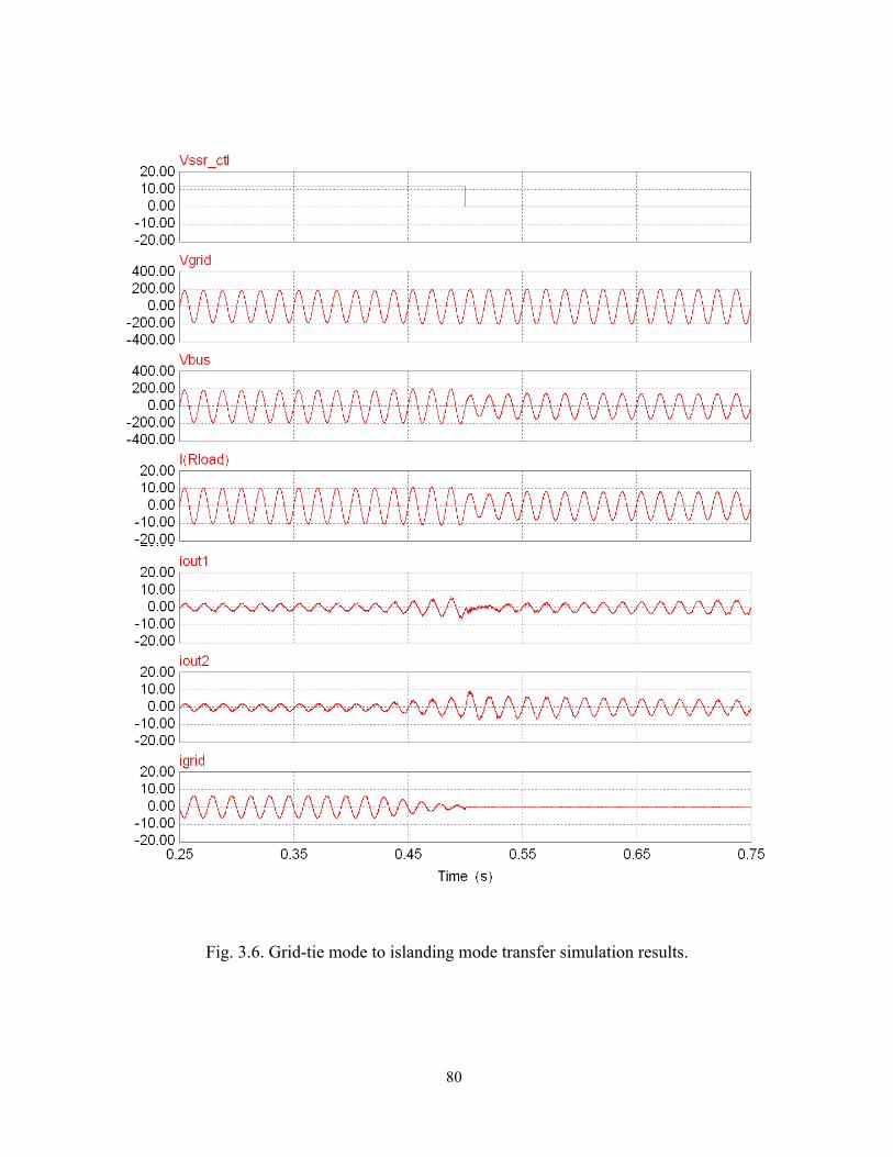
80
Fig. 3.6. Grid-tie mode to islanding mode transfer simulation results.

81
iout1
iout210A
10A
Vssr_ctl
vgrid
vbus
10Aiload
200V
200V
10V
t:50ms/div
10Aigrid
iout1
iout210A
10A
Vssr_ctl
vgrid
vbus
10Aiload
200V
200V
10V
t:50ms/div
10Aigrid
Fig. 3.7. Grid-tie mode to islanding mode transfer experimental results.

82
Fig. 3.8 shows the experimental result of bus voltage synchronization transition
before the microgrid system reconnecting to the grid. Once the grid voltage recovers to a
preset value, commanded by the upper-level controller through CAN bus, the inverter 1
starts to synchronize the magnitude and phase of bus voltage vbus to vgrid. Fig. 3.9 and Fig.
3.10 show the simulation and experimental results of the paralleled-inverter microgrid
system transferring from the islanding to grid-tie mode. If the phase and magnitude are
synchronized, the upper-level controller turns on the switch SSR by changing Vssr_ctl at the
next zero crossing. By commanding through the CAN bus from the upper-level controller,
the inverter 1 switches from voltage to current controller at the same zero crossing. The
current reference in inverter 1 after the mode transfer is intentionally set so that only a
small current is shown in igrid to minimize the switching transient. No noticeable transients
are observed in vbus and iload which indicates the parallel-inverter microgrid system is
capable of transferring from the islanding mode to grid-tie mode smoothly.

83
200V
vgridvbus
Vsyn
200V
vgridvbus
Vsyn
Fig. 3.8. Bus voltage synchronization transition before the micorgrid reconnecting to the
grid.
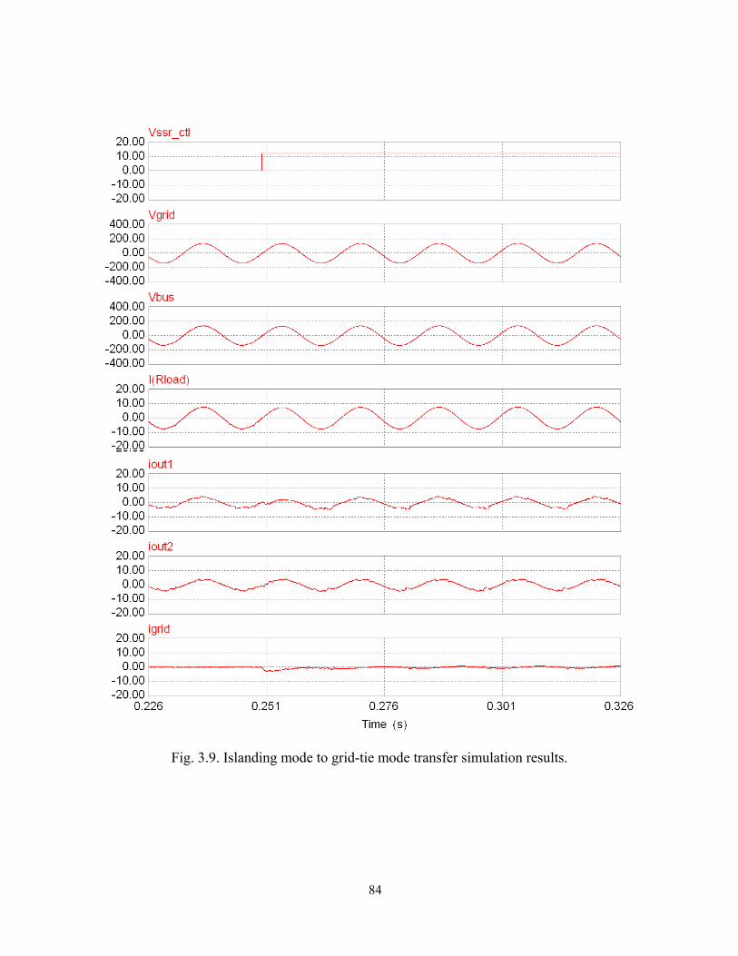
84
Fig. 3.9. Islanding mode to grid-tie mode transfer simulation results.
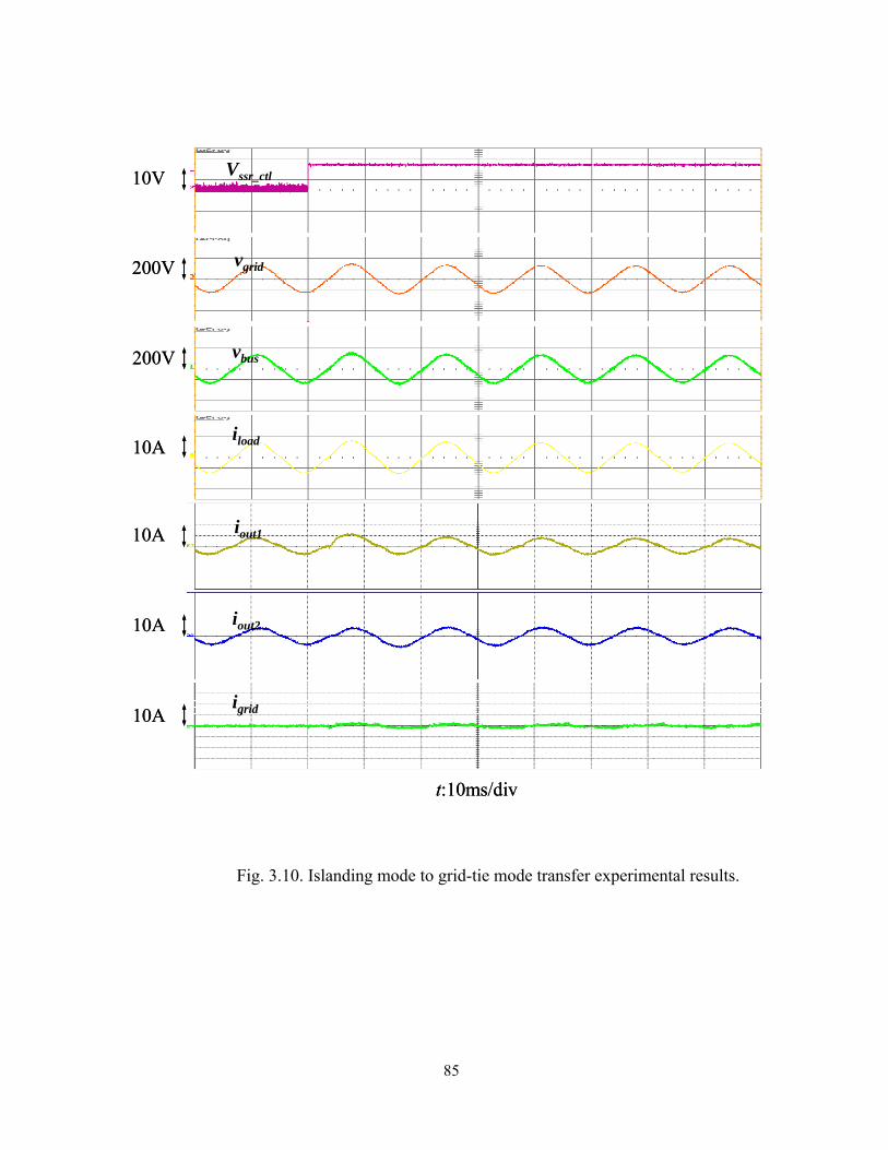
85
iout1
iout210A
10A
Vssr_ctl
vgrid
vbus
10Aiload
200V
200V
10V
t:10ms/div
10Aigrid
iout1
iout210A
10A
Vssr_ctl
vgrid
vbus
10Aiload
200V
200V
10V
t:10ms/div
10Aigrid
Fig. 3.10. Islanding mode to grid-tie mode transfer experimental results.

86
3.6 Summary
This chapter presents a complete design and implementation of an experimental
microgrid with paralleled power conditioning systems operating in the grid-tie mode,
islanding mode, and mode transfer. Key features of the proposed microgrid system are
summarized as follows:
1. Equal current sharing and synchronization
With the use of the CAN bus, the transmitted current magnitude is served as a
reference to adjust the current reference to the rest of inverters so that every inverter
shares the current equally. The phase synchronization is implemented with PLL and an
automatic phase adjustment to synchronize the output currents among the inverters.
2. Smooth mode transfer between the grid-tie and islanding modes
Key considerations for a seamless transfer are provided by applying basic circuit
laws. Proper mode transfer procedures with smooth current transition are suggested to
minimize the excessive electrical stresses.
Simulation and experimental results show that the output currents are equally shared
among different inverters without a noticeable circulating current by the use of the
proposed synchronization and upper-level control methods. Both the mode transfer
simulation and experimental results show that the multi-inverter based microgrid system
can switch between the grid-tie and islanding modes smoothly to ensure an uninterrupted
power supply to the critical loads.

87
The successful system operations suggest that the proposed parallel-inverter system
design with the LCL filter based inverters, mix of the dual- and single-loop voltage and
current controllers, PLL synchronization and CAN bus communication architecture can be
extended to microgrid or smartgrid applications.
88
Chapter 4
State-Space Modeling, Analysis, and Implementation of Paralleled Inverters for Microgrid Applications
4.1 Introduction
In this chapter, a state-space model of the previous proposed power conditioning
system will be performed so as to study the system stability under various conditions.
Eigenvalues with different controller gains and load conditions for both grid-tie mode and
standalone mode will be analyzed. The state-space model will also be extended to a
parallel-inverter system for the investigation of the load variation effects to the system
stability. A time-domain current ripple criterion is also suggested for the light-load
operation of the parallel-inverter microgrid system.
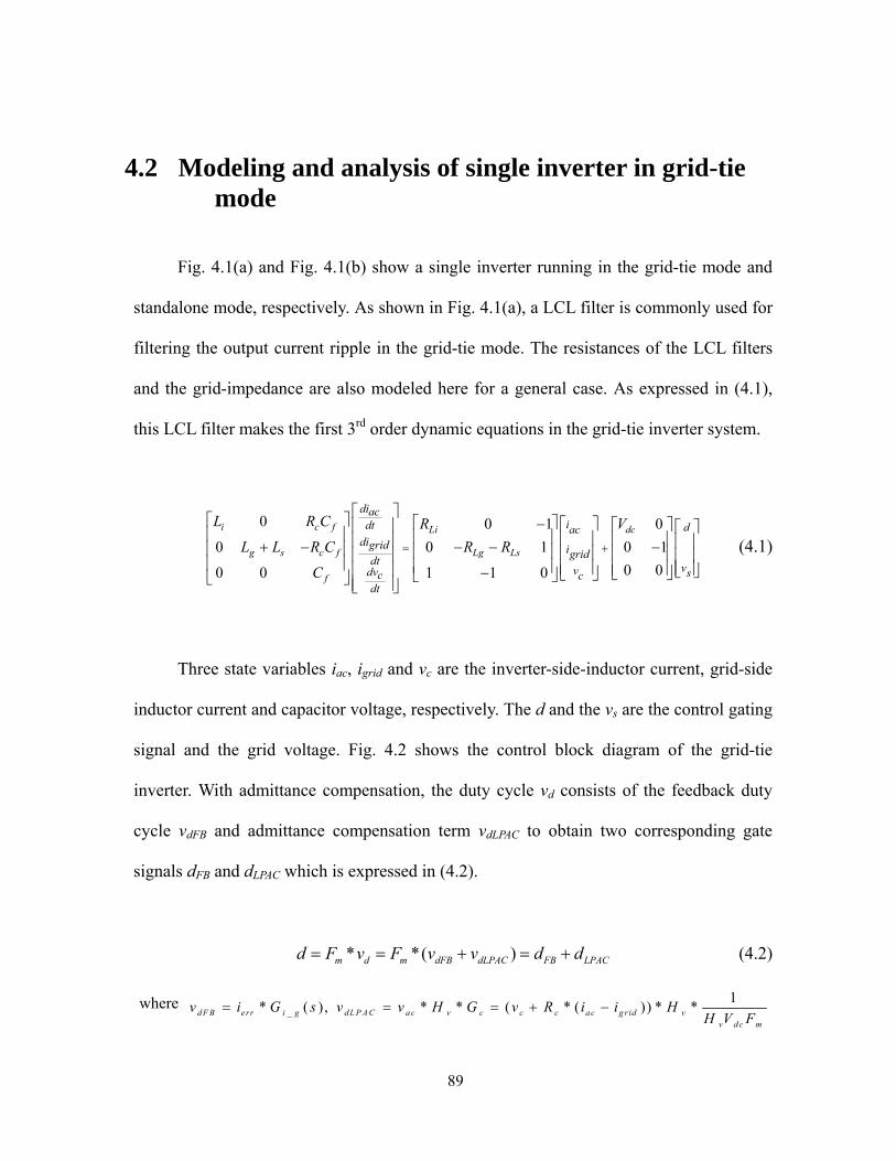
89
4.2 Modeling and analysis of single inverter in grid-tie mode
Fig. 4.1(a) and Fig. 4.1(b) show a single inverter running in the grid-tie mode and
standalone mode, respectively. As shown in Fig. 4.1(a), a LCL filter is commonly used for
filtering the output current ripple in the grid-tie mode. The resistances of the LCL filters
and the grid-impedance are also modeled here for a general case. As expressed in (4.1),
this LCL filter makes the first 3rd order dynamic equations in the grid-tie inverter system.
0 0 1 0
0 0 1 0 10 00 0 1 1 0
i c f Li dc
g s c f Lg Ls
f
diacidt dac
digrid igriddt vvdv sc cdt
L R C R VL L R C R R
C
= +
⎡ ⎤⎡ ⎤ ⎡ ⎤− ⎡ ⎤ ⎡ ⎤⎢ ⎥ ⎡ ⎤⎢ ⎥ ⎢ ⎥ ⎢ ⎥ ⎢ ⎥⎢ ⎥ ⎢ ⎥+ − − − −⎢ ⎥ ⎢ ⎥ ⎢ ⎥ ⎢ ⎥⎢ ⎥ ⎢ ⎥⎢ ⎥ ⎢ ⎥ ⎢ ⎥ ⎢ ⎥⎢ ⎥⎢ ⎥ ⎣ ⎦− ⎣ ⎦⎣ ⎦⎣ ⎦⎣ ⎦ ⎢ ⎥⎣ ⎦
(4.1)
Three state variables iac, igrid and vc are the inverter-side-inductor current, grid-side
inductor current and capacitor voltage, respectively. The d and the vs are the control gating
signal and the grid voltage. Fig. 4.2 shows the control block diagram of the grid-tie
inverter. With admittance compensation, the duty cycle vd consists of the feedback duty
cycle vdFB and admittance compensation term vdLPAC to obtain two corresponding gate
signals dFB and dLPAC which is expressed in (4.2).
* *( )m d m dFB dLPAC FB LPACd F v F v v d d= = + = + (4.2)
where _
1* ( ), * * ( * ( )) * *d F B err i g d L P A C a c v c c c ac g rid vv dc m
v i G s v v H G v R i i HH V F
= = = + −
90
d
igrid
Grid
Liiac Lgvac
Cfvi
Ls
vsvgrid
RLsRLgRLi
dc-acinverter
vc
Rc
ic
Vdc
d
igrid
Grid
Liiac Lgvac
Cfvi
Ls
vsvgrid
RLsRLgRLi
dc-acinverter
vc
Rc
ic
Vdc
(a)
Liiac Lgvac
Cfvi
RLgRLi
dc-acinverter
vc
Rc
ic
Vdc Load
iload
vbus
Liiac Lgvac
Cfvi
RLgRLi
dc-acinverter
vc
Rc
ic
Vdc Load
iload
vbus
(b)
Fig. 4.1. Single inverter hardware configuration: (a) grid-tie mode,
and (b) standalone mode.
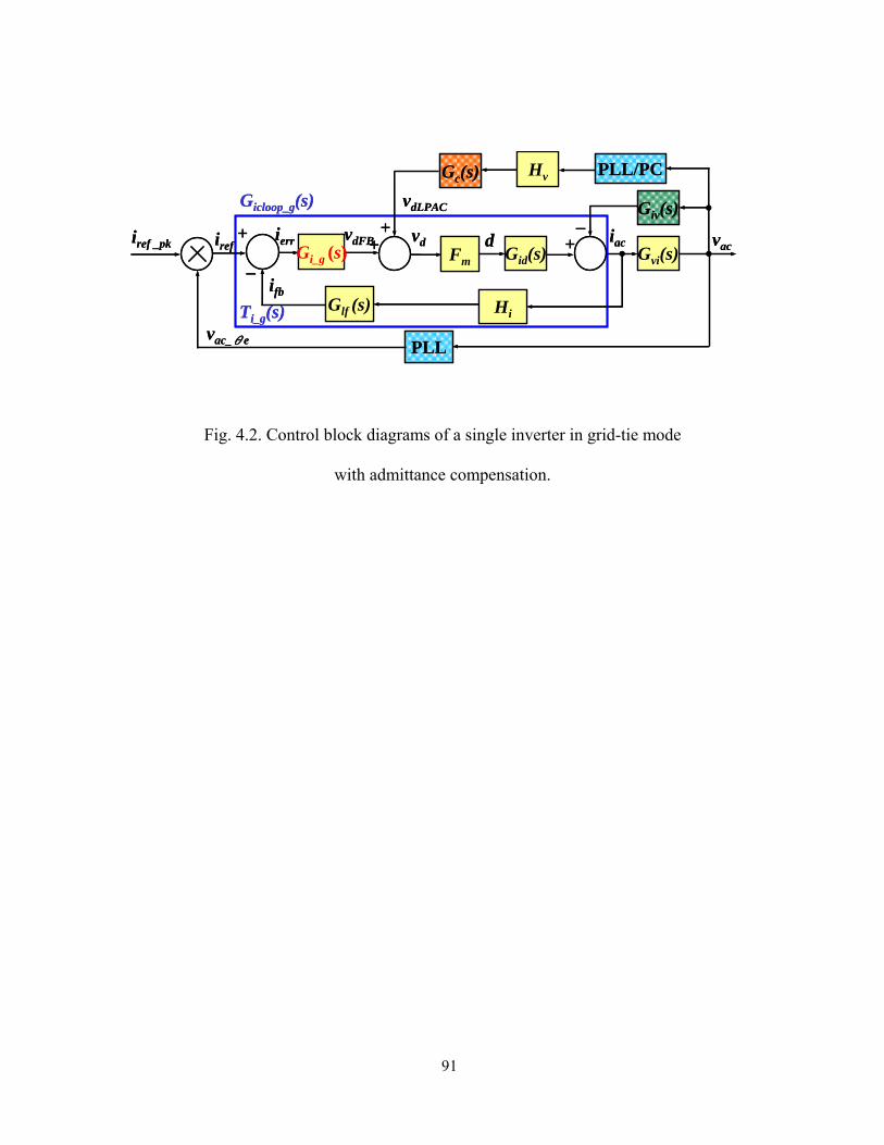
91
vac
ifb
vdierr
_
+FmGi_g (s)
iacdGid(s) Gvi(s)
Glf (s) HiTi_g(s)
+–
Giv(s)Gicloop_g(s)
++
Gc(s)vdLPAC
vdFB
PLL/PCHv
irefiref _pk
PLLvac_θe
vac
ifb
vdierr
_
+FmGi_g (s)
iacdGid(s) Gvi(s)
Glf (s) HiTi_g(s)
+–
Giv(s)Gicloop_g(s)
++
Gc(s)vdLPAC
vdFB
PLL/PCHv
irefiref _pk
PLLvac_θe
Fig. 4.2. Control block diagrams of a single inverter in grid-tie mode
with admittance compensation.

92
In Fig. 4.2, Hi and Glf(s) are the current feedback gain, and the hardware low-pass
filters’ transfer function. This feedback network contributes to another third-order
differential equation shown in (4.3).
1
2
00 10 0 2
00
ANF i ac
di fbdt
diHAdt
diHAdt
i fbHWF HWFiHWF HWF HAiANF HA H i
ω ωω ω
ω ω=
⎡ ⎤⎡ ⎤−⎢ ⎥⎢ ⎥
− +⎢ ⎥⎢ ⎥⎢ ⎥⎢ ⎥−⎣ ⎦ ⎣ ⎦
⎡ ⎤⎡ ⎤⎢ ⎥⎢ ⎥⎢ ⎥⎢ ⎥⎢ ⎥⎢ ⎥⎣ ⎦⎢ ⎥⎣ ⎦
(4.3)
Here Hi is a pure gain while the Glf(s) contains a second-order hardware filter and a
first-order anti-aliasing filter. Variables ωHWF and ωANF are the cut-off angular frequencies
for the hardware filter and the anti-aliasing filter, respectively. Currents iHA1 and iHA2 are
the two intermediate states of the hardware filters. The Gi_g(s) and Fm are the current
controller in grid-tie mode and the DSP PWM modulation gain, respectively. Gi_g(s) is
designed to be a proportional-resonant (PR) controller to achieve a low steady-state-error
output. As shown in (4.4), the PR controller can be represented as a second-order equation.
2 _ _ _
0 1 0 02 1 1
11
22 21
*( ) 2 * , * *sindFB pg ref fb c rg pr ref ref pk ac e ref pk e
i
dipr i ipr refdtdipr ic pr fb
dt
v k i i k i i i v iθ
ω ω
ω θ
+= − − −
⎡ ⎤ ⎡ ⎤ ⎡ ⎤⎡ ⎤ ⎡ ⎤⎢ ⎥ ⎢ ⎥ ⎢ ⎥⎢ ⎥ ⎢ ⎥⎣ ⎦⎢ ⎥ ⎣ ⎦ ⎣ ⎦ ⎣ ⎦⎣ ⎦= − + = =
(4.4)
Here kpg and krg are the proportional and resonant gains for the grid-tie mode
controller. ωc and ω1 are the equivalent bandwidth and fundamental angular frequency,
respectively. State variables ipr1 and ipr2 are two intermediate variables that represent the
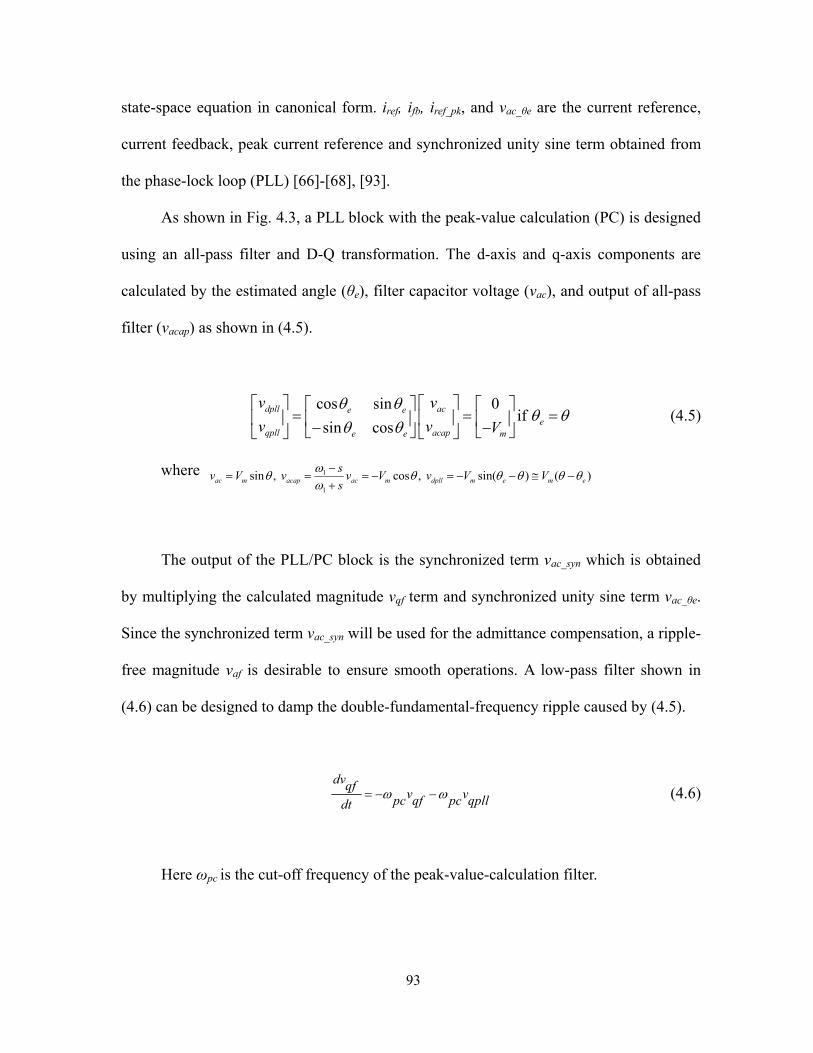
93
state-space equation in canonical form. iref, ifb, iref_pk, and vac_θe are the current reference,
current feedback, peak current reference and synchronized unity sine term obtained from
the phase-lock loop (PLL) [66]-[68], [93].
As shown in Fig. 4.3, a PLL block with the peak-value calculation (PC) is designed
using an all-pass filter and D-Q transformation. The d-axis and q-axis components are
calculated by the estimated angle (θe), filter capacitor voltage (vac), and output of all-pass
filter (vacap) as shown in (4.5).
cos sin 0
if sin cos
dpll ace ee
qpll acape e m
v vv v V
θ θθ θ
θ θ⎡ ⎤ ⎡ ⎤⎡ ⎤ ⎡ ⎤
= = =⎢ ⎥ ⎢ ⎥⎢ ⎥ ⎢ ⎥− −⎣ ⎦ ⎣ ⎦⎣ ⎦ ⎣ ⎦ (4.5)
where 1
1
sin , cos , sin( ) ( )ac m acap ac m dpll m e m esv V v v V v V Vs
ωθ θ θ θ θ θω
−= = = − = − − ≅ −
+
The output of the PLL/PC block is the synchronized term vac_syn which is obtained
by multiplying the calculated magnitude vqf term and synchronized unity sine term vac_θe.
Since the synchronized term vac_syn will be used for the admittance compensation, a ripple-
free magnitude vaf is desirable to ensure smooth operations. A low-pass filter shown in
(4.6) can be designed to damp the double-fundamental-frequency ripple caused by (4.5).
dvqf v vpc qf pc qplldt
ω ω= − − (4.6)
Here ωpc is the cut-off frequency of the peak-value-calculation filter.
94
D-QTransformation
vac
Gap(s)Gfpc(s)
vacap
vdPLL
vqPLL vqf
Gcpll(s) ++
++∫
vdnom
00 __
++
vdnom
sinvac_θe vac_synωe
ω1
ωdif θe
D-QTransformation
vac
Gap(s)Gfpc(s)
vacap
vdPLL
vqPLL vqf
Gcpll(s) ++
++∫
vdnom
00 __
++
vdnom
sinvac_θe vac_synωe
ω1
ωdif θe
Fig. 4.3. Control block diagrams of the phase-lock loop with the peak-value calculation.

95
Notice that equation (4.6) is a low-pass filter with a negative sign which makes the
state variable vqf in steady state equal to the positive voltage magnitude, Vm. In order to
design a universal PLL with a wide input voltage range, the normalized signal vdnom is
utilized as the feedback signal for the PLL. With an integrator as the PLL plant, a
controller Gcpll(s) is designed to have a 28-Hz cross-over frequency with a 36o phase
margin. A second-order equation for the PLL controller and plant is shown in (4.7).
00 01 01 0 1 0 1 0
1 1k k k
v
d difpll pll pll dif pll pll pll dif pll plldt
d e dnom edt
ω ω ω ω ω ω ωθ θθ
ωω ω
θ− − −
=
⎡ ⎤⎡ ⎤ ⎡ ⎤ ⎡ ⎤ ⎡ ⎤ ⎡ ⎤⎡ ⎤ ⎡ ⎤ ⎡ ⎤⎢ ⎥ + = +⎢ ⎥ ⎢ ⎥ ⎢ ⎥ ⎢ ⎥ ⎢ ⎥⎢ ⎥ ⎢ ⎥ ⎢ ⎥⎣ ⎦ ⎣ ⎦ ⎣ ⎦⎢ ⎥ ⎣ ⎦ ⎣ ⎦ ⎣ ⎦ ⎣ ⎦ ⎣ ⎦
⎣ ⎦
(4.7)
where s in ( ) 0 if d p ll m ed n o m e e
q f m
v Vvv V
θ θ θ θ θ θ−= = = − = ≅
Here ωpll, kpll are the cut-off frequency and gain of the PLL controller. Equations
(4.1) to (4.7) describe the dynamic behavior of a single-phase inverter in the grid-tie mode.
The above functions can be linearized and the small-signal perturbation can be applied to
derive the small signal model of the grid-tie inverter shown in (4.8).
g g g g gX A X B UΔ = Δ + Δ (4.8)
where ,1 2 1 2 _ac grid c fb HA HA pr pr dif e qfX UT T
i vref pk sg gi i v i i i i i vω θ= = ⎡ ⎤Δ Δ⎣ ⎦⎡ ⎤Δ Δ Δ Δ Δ Δ Δ Δ Δ Δ Δ Δ Δ⎣ ⎦
Here Xg, Ag, Bg and Ug are the state variable, state matrix, input matrix and system
input to the grid-tie inverter system. In order to find the potential instability causes of the
constructed model, the complete system eigenvalues are plotted in Fig. 4.4. With the

96
designed proportional gain kpg = 0.78, Fig. 4.4(a) shows that none of the eigenvalue is
located in the right-hand plane, and the system is stable. Notice that the system
eigenvalues keep at almost the same positions when the current reference magnitude iref_pk
changes from 20% to full load, which suggests that the stability of grid-tie mode is not
related much to a load change. By varying kpg, however, the system becomes unstable
when kpg exceeds 16 as shown in Fig. 4.4(b).

97
-4 -3 -2 -1 0105
-3
-2
-1
0
1
2
3 x 104x 10x 1044
x 10x 1055Real (1/sec)Real (1/sec)
Imag
inar
y (
Imag
inar
y ( r
adrad /
sec)
/sec
)
HW filter
AN filter
LCL filter
LCL filterHW filter
PR Controller
PLL/PC
-4 -3 -2 -1 0105
-3
-2
-1
0
1
2
3 x 104x 10x 1044
x 10x 1055Real (1/sec)Real (1/sec)
Imag
inar
y (
Imag
inar
y ( r
adrad /
sec)
/sec
)
HW filter
AN filter
LCL filter
LCL filterHW filter
PR Controller
PLL/PC
(a)
-20000 -15000 -10000 -5000 0 50000
2
4
6
8
10 x 104
kkpgpg = 16= 16
kkpgpg = 0.78= 0.78
kkpgpg increasingincreasing
Real (1/sec)Real (1/sec)
Imag
inar
y (
Imag
inar
y ( r
adrad /
sec)
/sec
)
-20000 -15000 -10000 -5000 0 50000
2
4
6
8
10 x 104
kkpgpg = 16= 16
kkpgpg = 0.78= 0.78
kkpgpg increasingincreasing
Real (1/sec)Real (1/sec)
Imag
inar
y (
Imag
inar
y ( r
adrad /
sec)
/sec
)
(b)
Fig. 4.4. Eigenvalue of grid-tie inverter (a) complete eigenvalue for kpg = 0.78,
and (b) the critical eigenvalue changes with varying kpg from 0.78 to 16.

98
4.3 Modeling and analysis of single inverter in standalone mode
Fig. 4.1(b) shows the hardware configuration of a single inverter in the standalone
mode. If the load is only a pure resistor with resistance Rload, then the plant equation can
be expressed by a third-order system, as shown in (4.9).
[ ]0 0 1
0 0 1 000 0 1 1 0
i c f Li dc
g c f Lg load
f
diacdt iac
diload iloaddtvdv cc
dt
L R C R VL R C R R d
C
= +
⎡ ⎤⎡ ⎤ ⎡ ⎤−⎢ ⎥ ⎡ ⎤⎡ ⎤⎢ ⎥ ⎢ ⎥⎢ ⎥ ⎢ ⎥⎢ ⎥− − −⎢ ⎥ ⎢ ⎥⎢ ⎥ ⎢ ⎥⎢ ⎥⎢ ⎥ ⎢ ⎥⎢ ⎥ ⎢ ⎥⎢ ⎥− ⎣ ⎦ ⎣ ⎦⎣ ⎦⎢ ⎥⎣ ⎦ ⎢ ⎥⎣ ⎦
(4.9)
Fig. 4.5 shows that an outer voltage loop is used to regulate the output voltage while
an inner current loop is adopted to damp the LCL resonance poles. As shown in (4.10), the
current controller in the standalone mode Gi_s(s) is designed as a first-order low-pass filter
to damp the LCL resonance.
1* 0.5 *dFBSWF d SWF err
dv v idt
ω ω= − + (4.10)

99
iifbfb
vvddiierrerr
__
++FFmmGGi_si_s ((ss))
iiacacddGGidid(s(s)) GGvivi(s(s))
GGlflf (s)(s) HHiiTTi_si_s(s(s))
++––
GGiviv(s(s))GGicloop_sicloop_s(s(s))
++++
GGcc(s(s))vvdLPACdLPAC
vvdFBdFB
PLL/PCPLL/PCHHvv
iirefref
GGlflf (s)(s) HHvv
vvrefref
vvfbfb
vverrerr
__++ GGvv((ss))
iifbfb
vvddiierrerr
__
++FFmmGGi_si_s ((ss))
iiacacddGGidid(s(s)) GGvivi(s(s))
GGlflf (s)(s) HHiiTTi_si_s(s(s))
++––
GGiviv(s(s))GGicloop_sicloop_s(s(s))
++++
GGcc(s(s))vvdLPACdLPAC
vvdFBdFB
PLL/PCPLL/PCHHvv
iirefref
GGlflf (s)(s) HHvv
vvrefref
vvfbfb
vverrerr
__++ GGvv((ss))
Fig. 4.5. Control block diagrams of a single inverter in standalone mode
with admittance compensation.

100
The voltage loop also contains a third-order filter Glf(s) with a similar equation as
expressed in (4.3) except that the currents variables change to the voltage variables. In
order to achieve a high loop gain at the fundamental frequency to minimize the steady-
state error, the voltage controller Gv(s) is also designed to be a PR controller which leads
to a second-order equation that has a similar form in (4.4) except that the current variables
change to the voltage ones. The current reference generation can be represented in (4.11).
2*( ) 2 *ref ps ref fb c rs pri k v v k vω= − + (4.11)
Here vref is the voltage reference. The above transfer functions from (4.9) to (4.11)
can be linearized and the small-signal perturbations can be applied to derive the small-
signal model of the standalone-mode inverter shown in (4.12).
s s s s sX A X B UΔ = Δ + Δ (4.12)
where 1 2 1 2 1 2 ,TT
ac load c fb HA HA dFB fb HA HA pr pr dif e qfX U vrefs si i v i i i v v v v v v vω θ= = ⎡ ⎤Δ⎣ ⎦⎡ ⎤Δ Δ Δ Δ Δ Δ Δ Δ Δ Δ Δ Δ Δ Δ Δ Δ Δ⎣ ⎦
Here Xs, As, Bs and Us are the state variable, state matrix, input matrix and system
input corresponding to the inverter in the standalone mode. The complete system
eigenvalues are shown in Fig. 4.6 to validate the state-space model. Fig. 4.6(a) shows that
the system is stable with the designed proportional gain kps = 0.02. With varying kps and
Rload, Fig. 4.6(b) suggests that the system become more unstable when Rload increases or
when kps increases. With kps = 2, the seventh points on Fig. 4.6(b) indicates that the system
is stable for Rload = 13.5 Ω, but not for Rload = 27 Ω.
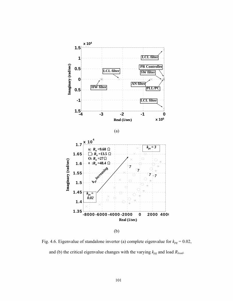
101
-4 -3 -2 -1 0105
1.5
-1
0.5
0
0.5
1
1.5 x 104x 10x 1044
Real (1/sec)Real (1/sec)
Imag
inar
y (
Imag
inar
y ( r
adrad /
sec)
/sec
)
x 10x 1055
HW filterAN filter
LCL filter
LCL filter
LCL filter SW filterPR Controller
PLL/PC
-4 -3 -2 -1 0105
1.5
-1
0.5
0
0.5
1
1.5 x 104x 10x 1044
Real (1/sec)Real (1/sec)
Imag
inar
y (
Imag
inar
y ( r
adrad /
sec)
/sec
)
x 10x 1055
HW filterAN filter
LCL filter
LCL filter
LCL filter SW filterPR Controller
PLL/PC
(a)
-8000 -6000 -4000 -2000 0 2000 40001.35
1.4
1.45
1.5
1.55
1.6
1.65
1.7 x 10⁴
x: x: RRoo =9.68 =9.68 ΩΩ: : RRoo =13.5 =13.5 ΩΩO: O: RRoo =27=27ΩΩ﹡﹡::RRoo =48.4 =48.4 ΩΩ
kk pspsincre
asing
increasi
ng
kkpsps = 3= 3
kkpsps = = 0.020.02
7777
77 77
Real (1/sec)Real (1/sec)
Imag
inar
y (
Imag
inar
y ( r
adrad /
sec)
/sec
)
-8000 -6000 -4000 -2000 0 2000 40001.35
1.4
1.45
1.5
1.55
1.6
1.65
1.7 x 10⁴
x: x: RRoo =9.68 =9.68 ΩΩ: : RRoo =13.5 =13.5 ΩΩO: O: RRoo =27=27ΩΩ﹡﹡::RRoo =48.4 =48.4 ΩΩ
kk pspsincre
asing
increasi
ng
kkpsps = 3= 3
kkpsps = = 0.020.02
7777
77 77
-8000 -6000 -4000 -2000 0 2000 40001.35
1.4
1.45
1.5
1.55
1.6
1.65
1.7 x 10⁴
x: x: RRoo =9.68 =9.68 ΩΩ: : RRoo =13.5 =13.5 ΩΩO: O: RRoo =27=27ΩΩ﹡﹡::RRoo =48.4 =48.4 ΩΩ
kk pspsincre
asing
increasi
ng
kkpsps = 3= 3
kkpsps = = 0.020.02
7777
77 77
Real (1/sec)Real (1/sec)
Imag
inar
y (
Imag
inar
y ( r
adrad /
sec)
/sec
)
(b)
Fig. 4.6. Eigenvalue of standalone inverter (a) complete eigenvalue for kpg = 0.02,
and (b) the critical eigenvalue changes with the varying kpg and load Rload.

102
4.4 Modeling and analysis of parallel inverters with the current sharing controller
Fig. 4.7 shows the hardware of the mircogrid system in the islanding mode. As
shown in Fig. 4.8, the state-space model of the mircogrid system in the islanding mode
can be obtained by combining the derived equations in above sections and the current
sharing controller. In order to extend the transmission distance, the transmitted signal is a
frequency-decoupled current magnitude. The frequency information does not need to be
transmitted because it will be automatically tracked by the PLL. As shown in Fig. 4.8, a
PC block is used to calculate the frequency-decoupled current magnitude information for
the current sharing.
Assume that the load is only a pure resistor, then estimated phases in voltage PLL
can be used to calculate the current magnitude similar to the approach shown in (4.5)
except the input becomes currents, iac1 and iac2. After the D-Q transformations, two low-
pass filters with the similar expression in (4.6) are utilized to filter the double-
fundamental-frequency ripples. Once the transmitted current magnitude of the voltage-
controlled inverter (iout1_pk) and the calculated magnitude of the current-controlled inverter
(iout2_pk) are obtained, the automatic reference generation (ARG) adjusts the current
reference magnitude of the current-controlled inverter iref2_pk to share the inverter currents.
The ARG control algorithm can be implemented digitally as described in chapter 3 or a
simple proportional-integral (PI) controller in (4.13).

103
2_ 1_ 2_ ref pk ac pk ref offseti i i= + (4.13)
2 _ 1_ 2 _1where ( )* ( )
1w
ref offset ac pk ac pk pcs icsw
sTi i i k ksT s
⎡ ⎤= − +⎢ ⎥+⎣ ⎦
Here iref2_offset is the offset of the current reference. Tw, kpcs, kpis are the washout-term
time constant, proportional gain and integral gain of the PI controller. By combining state-
state equations from (4.1) to (4.13) and applying the perturbations to these equations, the
complete small-signal model of the parallel-inverter system can be derived in (4.14).
i i i i iX A X B UΔ = Δ + Δ (4.14)
where
1 1 1 1 11 21 1 1 11 21
11 21 1 1 1 2 2 2 2 12
22 12 22 2 2 2 1_ 2 _ 2 _
ac load c fb HA HA dFB fb HA HA
pr pr dif e qf ac grid c fb HA
T
HA pr pr dif e qf ac pk ac pk ref pk
X
U
i
vrefi
i i v i i i v v v v
v v v i i v i i
i i i v i i i
ω θ
ω θ
=
= Δ
⎡Δ Δ Δ Δ Δ Δ Δ Δ Δ Δ Δ⎣
Δ Δ Δ Δ Δ Δ Δ Δ Δ Δ
⎤Δ Δ Δ Δ Δ Δ Δ Δ Δ ⎦
ΔT
⎡ ⎤⎣ ⎦
Here Xi, Ai, Bi and Ui are the state variable, state matrix, input matrix, and system
input correspondingly of the microgrid system in the islanding mode.

104
Liiac1 iout1Lg
vac1Cf vbusvi1RLoadiload
inverter1
Liiac2 iout2Lg
vac2Cf vbusvi2inverter
2
Liiacn ioutnLg
vacnCf vbusvin
invertern
dc-dcconverter
Vin-1 Vdc1
dc-dcconverterVin-2 Vdc2
dc-dcconverterVin-n Vdcn
Liiac1 iout1Lg
vac1Cf vbusvi1RLoadiload
inverter1
Liiac2 iout2Lg
vac2Cf vbusvi2inverter
2
Liiacn ioutnLg
vacnCf vbusvin
invertern
dc-dcconverter
Vin-1 Vdc1
dc-dcconverterVin-2 Vdc2
dc-dcconverterVin-n Vdcn
Fig. 4.7. The hardware of parallel-inverter microgrid system in islanding mode.
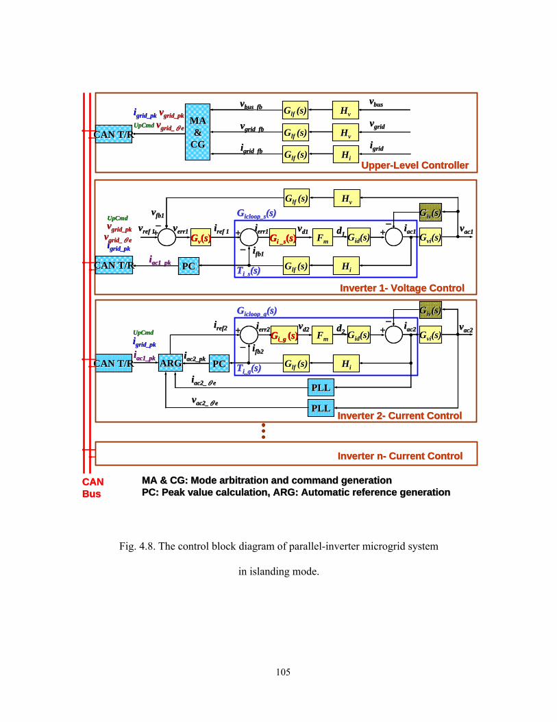
105
iifb1fb1
vvd1d1iierr1err1
__++ FFmmGGii __ss((ss))
iiac1ac1dd11 GGidid(s(s)) GGvivi(s(s))vvac1ac1
GGlflf (s)(s) HHiiTTi_si_s(s(s))
++––
GGiviv(s(s))GGicloop_sicloop_s(s(s))
iiref2 ref2
iifb2fb2
vvd2d2iierr2err2
__++ FFmmGGi_gi_g ((ss))
iiac2ac2dd22 GGidid(s(s)) GGvivi(s(s))vvac2ac2
GGlflf (s)(s) HHiiTTi_gi_g(s(s))
++––
GGiviv(s(s))GGicloop_gicloop_g(s(s))
Inverter 1Inverter 1-- Voltage ControlVoltage Control
PLLPLL
PLLPLL
CAN T/RCAN T/R
Inverter 2Inverter 2-- Current ControlCurrent Control
Inverter nInverter n-- Current ControlCurrent Control
CAN CAN BusBus
MA & CG: Mode arbitration and command generationMA & CG: Mode arbitration and command generationPC: Peak value calculation, ARG: Automatic reference generationPC: Peak value calculation, ARG: Automatic reference generation
PCPCiiac1_pkac1_pkCAN T/RCAN T/R
PCPCARGARGiiac1_pkac1_pk iiac2_pkac2_pk
iiac2_ac2_θθee
vvac2_ac2_θθee
GGlflf (s)(s) HHii
CAN T/RCAN T/Riigrid_fbgrid_fb
iigridgrid
UpCmdUpCmd
UpCmdUpCmd
UpperUpper--Level ControllerLevel Controller
iirefref 1 1 vvrefref 1 1
vvfb1fb1
vverr1err1__
++ GGvv((ss))
GGlflf (s)(s) HHvv
UpCmdUpCmd
GGlflf (s)(s) HHvvvvgrid_fbgrid_fb
vvgridgrid
GGlflf (s)(s) HHvvvvbus_fbbus_fb
vvbusbusiigrid_pkgrid_pk
iigrid_pkgrid_pk
iigrid_pkgrid_pk
vvgrid_pkgrid_pkvvgrid_grid_θθee
vvgrid_grid_θθee
vvgrid_pkgrid_pk
MAMA&&
CGCG
Fig. 4.8. The control block diagram of parallel-inverter microgrid system
in islanding mode.

106
Fig. 4.9(a) shows that the system is stable with the designed controller gains at
about 16% load or Rload = 27 Ω. Fig. 4.9(b) suggests that the system stays stable from 8%
load (Rload = 54 Ω) to 100% load (Rload = 4.5 Ω). Another observation is that the
eigenvalues in Fig. 4.9 stay almost unchanged regardless of the variations of current-
sharing controller parameters kpcs and kpis. As shown in (4.13), iref_offset is close to zero
because iac1_pk almost equals iac2_pk during the steady state. However, the current-sharing
controller parameters, kpcs and kpis, will change the dynamic response when the output
current magnitudes, iac1_pk and iac2_pk, are not equal.

107
-4 -3 -2 -1 05
-3
-2
-1
0
1
2
3 x 10⁴
Real (1/sec)Real (1/sec)
Imag
inar
y (
Imag
inar
y ( r
adrad /
sec)
/sec
)
x 10x 1055
x 10x 1044
HW filter
HW filter
HW filter
LCL filter
LCL filter
LCL filter
LCL filter
LCL filter
AN filter
PR Controller
PLL/PC
SW filter
CSC
-4 -3 -2 -1 05
-3
-2
-1
0
1
2
3 x 10⁴
Real (1/sec)Real (1/sec)
Imag
inar
y (
Imag
inar
y ( r
adrad /
sec)
/sec
)
x 10x 1055
x 10x 1044
-4 -3 -2 -1 05
-3
-2
-1
0
1
2
3 x 10⁴
Real (1/sec)Real (1/sec)
Imag
inar
y (
Imag
inar
y ( r
adrad /
sec)
/sec
)
x 10x 1055x 10x 1055x 10x 1055
x 10x 1044x 10x 1044x 10x 1044
HW filter
HW filter
HW filter
LCL filter
LCL filter
LCL filter
LCL filter
LCL filter
AN filter
PR Controller
PLL/PC
SW filter
CSC
(a)
-14000 -12000 -10000 -8000 -6000 -4000 -2000-2
-1.5
-1
-0.5
0
0.5
1
1.5
2 x 10⁴
5454ΩΩ
4.54.5ΩΩ
5454ΩΩ
2727ΩΩ
13.513.5ΩΩ99ΩΩ66ΩΩ
4.54.5ΩΩ
66ΩΩ13.513.5ΩΩ99ΩΩ
2727ΩΩ
RRloadload increasingincreasing
Imag
inar
y (
Imag
inar
y ( r
adrad /
sec)
/sec
)
Real (1/sec)Real (1/sec)-14000 -12000 -10000 -8000 -6000 -4000 -2000
-2
-1.5
-1
-0.5
0
0.5
1
1.5
2 x 10⁴
5454ΩΩ
4.54.5ΩΩ
5454ΩΩ
2727ΩΩ
13.513.5ΩΩ99ΩΩ66ΩΩ
4.54.5ΩΩ
66ΩΩ13.513.5ΩΩ99ΩΩ
2727ΩΩ
RRloadload increasingincreasing
Imag
inar
y (
Imag
inar
y ( r
adrad /
sec)
/sec
)
Real (1/sec)Real (1/sec)
(b)
Fig. 4.9. Eigenvalues of the microgrid system in islanding mode (a) complete eigenvalues
for Rload = 27 Ω, and (b) the critical mode eigenvalue changes with varying Rload.
108
4.5 Simulation and experimental verification
Fig. 4.10 shows the simulation and experimental results of a single-phase inverter running
in the steady-state grid-tie mode at 3.2kW condition. Waveforms indicate that the system is
stable with the designed controllers (kpg = 0.78). Fig. 4.11 shows the transient simulation
and experimental results of a single inverter running in the grid-tie mode. With the designed
controller parameters, the system is stable even the output power changes from 1.8kW to
3.6kW which agrees with stability trend of the eigenvalue analysis shown in Fig. 4.4.
Notice the response in the grid-tie application is intentionally set in the second range
because the slow dynamic of the utility grid. With the increased controller gain (kpg = 16) in
the grid-tie mode, Fig. 4.12 shows the unstable results of the current loop which the current
loop output current iLi has a resonance around 14.5k Hz. Fig. 4.12(b) is the room-in result
of iLi waveform in Fig. 4.12(a). Fig. 4.12(c) and 4.12(d) shows the frequency spectrum and
the Bode plot result of this set of controller gain. The eigenvalue results in Fig 4.4(b) can be
verified by Fig. 4.12 which the resonance frequencies are almost the same. Notice that the
switching frequency of simulation in Fig. 4.12 is intend to set to a relative high switching
frequency, 200k Hz, in order to see this 14.5k Hz resonance. However, for the real
implementation, a 20k Hz switching frequency is chosen for the IGBT power device.

109
(a)
t:10ms/div
20A
300Vvac
igrid
t:10ms/div
20A
300Vvac
igrid
(b)
Fig. 4.10. Grid-tie mode results at 3.2 kW with kpg = 0.78 and krg = 97.5 (a) simulation
results, and (b) experimental results.

110
(a)
t:200ms/div
20A
300Vvac
igrid
t:200ms/div
20A
300Vvac
igrid
(b)
Fig. 4.11. Transient grid-tie mode results from 1.8 kW to 3.6kW
with kpg = 0.78 and krg = 97.5 (a) simulation results, and (b) experimental results.

111
(a)
0.0876 0.0878 0.088 0.0882 0.0884Time (s)
21
22
23
24
25
I(Li)
0.0879506 0.0880185
Δt = 0.0000679 secfres= 14.727k Hz
0.0876 0.0878 0.088 0.0882 0.0884Time (s)
21
22
23
24
25
I(Li)
0.0879506 0.0880185
Δt = 0.0000679 secfres= 14.727k Hz
(b)
Fig. 4.12. Grid-tie mode results at 3.2 kW with kpg = 16 and krg = 97.5 (a) time-domain
simulation result, (b) zoom in time-domain result.
0-10-20-30
102030
I(Li)
0-100-200-300
100200300
Vac
0.06 0.08 0.1 0.12 0.14Time (s)
0
-20
20
igrid

112
0 5000 10000 15000 20000 25000Frequency (Hz)
0
5
10
15
20
25
FFT I(Li)
fres= 14.587 k Hz
0 5000 10000 15000 20000 25000Frequency (Hz)
0
5
10
15
20
25
FFT I(Li)
fres= 14.587 k Hz
(c)
-50
0
50
100
G.M.: -0.16 dBFreq: 1.45e+004 HzUnstable loop
Mag
nitu
de (d
B)
Open-Loop Bode Editor (C)
101 102 103 104 105-360
-270
-180
-90
0
P.M.: -0.572 degFreq: 1.47e+004 Hz
Phas
e (d
eg)
Frequency (Hz)
fres= 14.492 k Hz
Ti(s)
-50
0
50
100
G.M.: -0.16 dBFreq: 1.45e+004 HzUnstable loop
Mag
nitu
de (d
B)
Open-Loop Bode Editor (C)
101 102 103 104 105-360
-270
-180
-90
0
P.M.: -0.572 degFreq: 1.47e+004 Hz
Phas
e (d
eg)
Frequency (Hz)
fres= 14.492 k Hz
Ti(s)
(d)
Fig. 4.12. Grid-tie mode results at 3.2 kW with kpg = 16 and krg = 97.5 (c) frequency
spectrum of time-domain waveform, and (d) the bode plot of current loop.

113
Fig. 4.13 shows the simulation and experimental results of a single-phase inverter
running in the steady-state standalone mode at 3.2kW condition. Waveforms indicate that
the system is stable with the designed controllers (kps = 0.02 and krs = 12) and this load
condition (Rload = 13.5 Ω). Fig. 4.14 shows the simulation and experimental results of
single-phase inverter running under the standalone-mode dynamic load step with the load
changing from Rload = 27 Ω to Rload = 13.5 Ω using kps = 0.02 and krs = 12. The waveforms
show that the system is stable with these controller parameters. Both simulation and
experimental results agree with the stability trend predicted by the eigenvalue analysis
shown in Fig. 4.6(b).
To further verify that the system can run unstable with an increased proportional
gain, as predicted in Fig. 4.6, the system was simulated using kps = 2 and krs = 12.
Simulation results shown in Fig. 4.15 indicate that initially when the load is 27 Ω, the
system is unstable. With the same controller, when the load is increased to Rload = 13.5 Ω,
the system becomes stable. This simulation result again validates the eigenvalue analysis
results shown in Fig. 4.6(b).
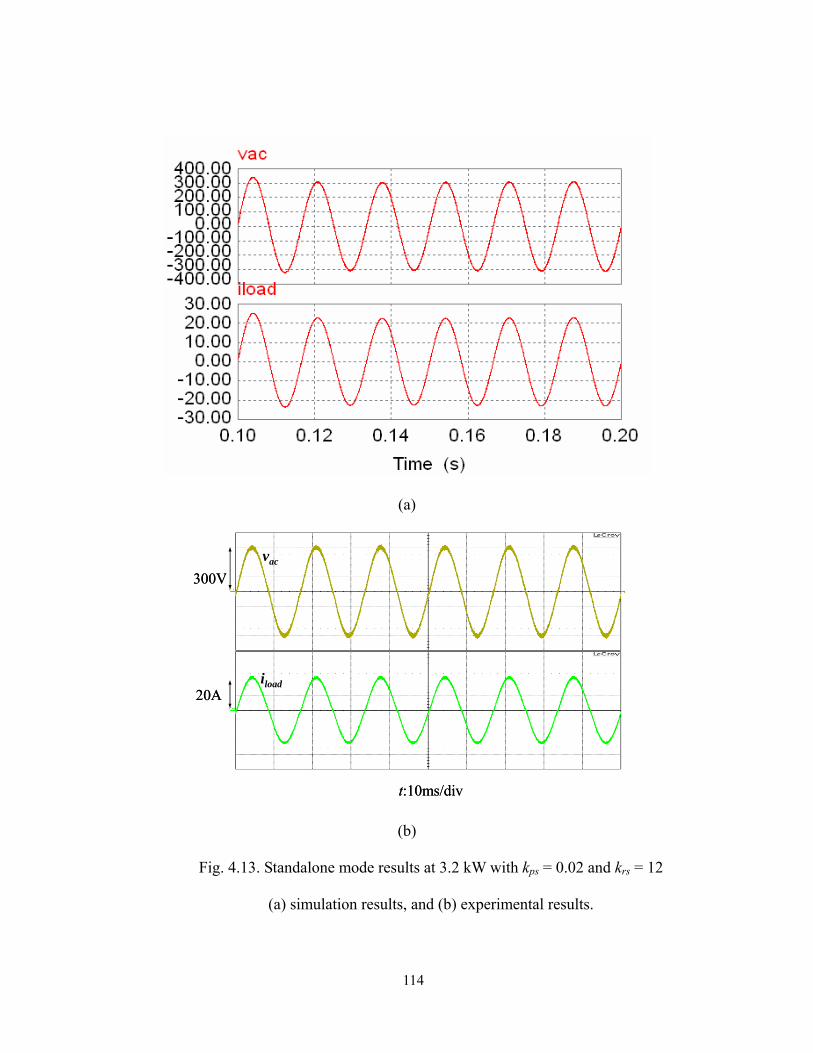
114
(a)
t:10ms/div
20A
300Vvac
iload
t:10ms/div
20A
300Vvac
iload
(b)
Fig. 4.13. Standalone mode results at 3.2 kW with kps = 0.02 and krs = 12
(a) simulation results, and (b) experimental results.

115
(a)
t:10ms/div
20A
300Vvac
iload
t:10ms/div
20A
300Vvac
iload
(b)
Fig. 4.14. Transient standalone mode results from Rload = 27 Ω to Rload = 13.5 Ω with kps =
0.02 and krs = 12 (a) simulation results, and (b) experimental results.
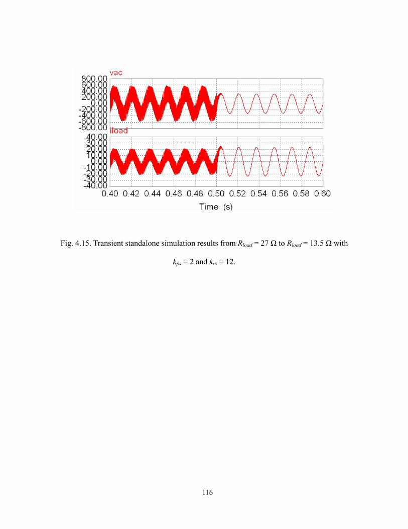
116
Fig. 4.15. Transient standalone simulation results from Rload = 27 Ω to Rload = 13.5 Ω with
kps = 2 and krs = 12.

117
Fig. 4.16 and Fig. 4.17 show the simulation and experimental results of the
mircogrid system in the islanding mode at light load (Rload = 54 Ω) and heavy load (Rload =
6 Ω), respectively. Waveforms suggest that the system is stable within this load range
which agrees with the stability trend of eigenvalue analysis in Fig. 4.9. Fig. 4.18 shows
the simulation and experimental results of the parallel-inverter system running under the
islanding-mode dynamic load step with the load changing from Rload = 27 Ω to Rload = 13.5
Ω. The waveforms show that the system is stable with the designed controller which
validates the eigenvalue analysis predictions shown in Fig. 4.9.

118
(a)
(b)
Fig. 4.16. Simulation results of the microgrid system in islanding mode
(a) Pout = 800 W (Rload = 54 Ω) and, (b) Pout = 7.4 kW (Rload = 6 Ω).

119
vbus
iload
iout1
t:10ms/div
40A iout2
40A
40A
300V vbus
iload
iout1
t:10ms/div
40A iout2
40A
40A
300V
(a)
vbus
iload
iout1
t:10ms/div
40A iout2
40A
40A
300V vbus
iload
iout1
t:10ms/div
40A iout2
40A
40A
300V
(b)
Fig. 4.17. Experimental results of the microgrid system in islanding mode
(a) Pout = 800 W (Rload = 54 Ω) and, (b) Pout = 7.4 kW (Rload = 6 Ω).

120
(a)
vbus
ioad
iout1
t:10ms/div
20A iout2
20A
20A
300V vbus
ioad
iout1
t:10ms/div
20A iout2
20A
20A
300V
(b)
Fig. 4.18. Transient results of the microgrid system in islanding mode from Rload = 27 Ω to
Rload = 13.5 Ω (a) simulation results, and (b) experimental results.
121
4.6 Summary
The state-space model and implementation results of a microgrid system operating
in the grid-tie mode, standalone mode and the parallel-inverter mode (islanding mode)
were presented in this chapter. Through the state-space analysis of the model, the
following conclusions can be drawn:
1. Eigenvalue analysis for grid-tie mode
The grid-tie system tends to be more unstable with increased proportional gain kpg
since the critical eigenvalue moves toward the right-half plane. The system eigenvalues
do not change much with the increased current reference magnitude which implies the
stability of grid-tie mode is not much related to the load change.
2. Eigenvalue analysis for the standalone mode
With the increased proportional gain kps and load resistance Rload, the standalone
system becomes more unstable; the critical eigenvalue moves closer to the right-half
plane.
3. Eigenvalue analysis for islanding mode
With the increased load resistance, Rload, the microgrid system in islanding mode
stays stable but the critical eigenvalue moves closer to the right-half plane. Changes in
current-sharing controller gains have very little effects on the steady-state eigenvalue
results.

122
With the designed controller parameters, experimental and simulation results show
the stable output waveforms in single-phase grid-tie mode, single-phase standalone mode
and the parallel-inverter microgrid system in islanding mode. With a higher controller gain
in the standalone mode, the simulation results show that the system is stable for the
heavier load condition but will become unstable in the lighter load condition. This agrees
with the stability trend in the eigenvalue analysis. For the grid-tie mode, the simulation
results also verify the model effectiveness by changing the controller gain. The eigenvalue
analysis of the parallel inverter system in islanding mode shows that the designed
controllers make the system stable from light load to heavy load. This analysis result of
the stable operation is confirmed by both the simulation and experimental results in the
proposed multi-inverter microgrid system.

123
Chapter 5
Conclusion and Future Works
5.1 Summary and major contributions
This dissertation presents a complete design and implementation of an experimental
microgrid with paralleled power conditioning systems operating in the grid-tie mode,
islanding mode, and mode transfers. Major contributions of the dissertation can be
summarized as follows:
1. The universal inverter is designed and implemented with the LCL filter which
successfully operates in both grid-tie and standalone mode without any hardware
modification.
2. In grid-tie mode, the reverse power flow issue during the grid-tie connection
transient is eliminated by the proposed admittance compensation. Precision steady-
state current control is achieved by adapting the high-gain PR controller.
3. In standalone mode, a dual-loop voltage controller with inner current loop is
designed to have the inherent current limitation to improve system reliability. Outer

124
voltage loop controller is designed with a PR controller to minimize the steady-
state error.
4. Equal current sharing among parallel inverters within the microgrid is fulfilled
through a frequency-coupled-signal transmission scheme without an extreme high
bandwidth communication channel. The phase synchronization is implemented
with PLL and an automatic phase adjustment.
5. Smooth mode transfers of a multiple-inverter microgrid system are achieved by the
proposed mode transfer algorithms based on the circuit principles to minimize the
excessive electrical stresses.
6. The state-space model and eigenvalue analysis are initially conducted in the single
inverter and extended to the parallel-inverter microgird system to investigate the
stability under system variations and optimize the trade-off between the
performance and stability.

125
5.2 Future works
1. Extending the developed control strategies in fuel-cell DGs to intermittent energy
sourced DGs by modifying the command generation section.
2. Incorporating a storage system into the proposed microgrid system to supply the
transient load requirement and allow the existence of the intermittent energy
sources in the islanding mode.
3. Applying the advanced control strategies such as sliding mode control to improve
the system dynamics and enhance the system immunity to the system disturbance
and parameter change.
4. Implementing an energy-management system in the existing microgrid system to
minimize the operation cost and enhance the system reliability.
126
5.3 Publications
C. L. Chen, Y. B. Wang, J. S. Lai, Y. S. Lee, and D. Martin, “Design of parallel
inverters for smooth mode transfer microgrid applications ,” IEEE Trans. Power
Electron., vol. 25, no. 1, pp. 6-15, Jan. 2010.
S. Y. Park, C. L. Chen, and J. S. Lai, “A wide-range active and reactive power
flow controller for a solid oxide fuel cell power conditioning system,” IEEE Trans.
Power Electron., vol. 23, pp. 2703-2707, Nov. 2008.
S. Y. Park, C. L. Chen, J. S. Lai, and S. R. Moon, “Admittance compensation in
current Loop control for a grid-tie LCL fuel cell inverter,” IEEE Trans. Power
Electron., vol. 23, pp. 1716-1723, July 2008.
C. L. Chen, Y. S. Lee, J. S. Lai and D. Martin, “State-space modeling, analysis, and
implementation of paralleled inverters for microgrid applications,” in Proc. of IEEE
APEC, Feb. 2010, pp. 619-626.
C. L. Chen, Y. B. Wang, and J. S. Lai, “Design of parallel inverters for smooth
mode transfer micogrid applications,” in Proc. of IEEE APEC, Feb. 2009, pp. 15-19.
C. L. Chen, J. S. Lai, Y. B. Wang, S. Y. Park, and H. Miwa, “Design and control
for LCL-based inverters with both grid-tie and standalone parallel operations,” in
Proc. of IEEE IAS, Oct. 2008, pp. 1-7.
S. Y. Park, C. L. Chen, and J. S. Lai, “A wide-range active and reactive power
flow controller for a solid oxide fuel cell power conditioning system,” in Proc. of
IEEE APEC, Feb. 2008, pp. 952 - 958.

127
C. L. Chen, S. Y. Park, J. S. Lai, S. Moon, “Admittance compensation in current
loop control for a grid-tie LCL fuel cell inverter,” in Proc. of IEEE PESC, Jun.
2007, pp. 520-526.
S. Y. Park, J. S. Lai, C. L. Chen, S.R. Moon and T-W. Chun, "Current loop control
with admittance compensation for a single-phase grid-tie fuel cell power
conditioning system," in Proc. of IEEE APEC, Feb. 2007, pp. 1010 - 1016.
J. S. Lai, S. Y. Park, S. R. Moon, and C. L. Chen, "A High-Efficiency 5-kW Soft-
switched power conditioning system for low-voltage solid oxide fuel cells", in Proc.
of IEEE PCC, April 2007, pp. 463 - 470.

128
References
[1] F. Blaabjerg, Z. Chen, and S. B. Kjaer, “Power electronics as efficient interface in
dispersed power generation systems,” IEEE Trans. Power Electron., vol. 19, no. 5, pp.
1184-1194, Sep. 2004.
[2] B. Maurhoff and G. Wood, “Dispersed generation to reduce power costs and improve
service reliability,” in Proc. of IEEE REPC, pp. C5/1-C5/7, 2000.
[3] J. Gutierrez-Vera, “Use of renewable sources of energy in Mexico,” IEEE Trans.
Energy Conv., vol. 9, pp. 442-450, Sept. 1994.
[4] L. Philipson, “Distributed and dispersed generation: addressing the spectrum of
consumer needs,” in Proc. of IEEE Power Engineering Society Summer Meeting, vol.
3, pp.1663-1665, 2000.
[5] G. T. Chinery and J. M. Wood, “Tva's photovoltaic activities,” IEEE Trans. Power
Appa. and Syst., vol. pas-104, pp. 1998-2005, Aug. 1985.
[6] Wind Power in Power Systems, Edited by Thomas Ackermann, J. Willy Press, 2003.
[7] Fuel Cell Fundamentals, R. P. O’Hayre, S.W. Cha, W. G. Colella, and F.B. Prinz, ,
New Jersey: Wiley, 2009.
[8] A. K. Saha, S. Chowdhury, S. P. Chowdhury, and P. A. Crossley , “Modeling and
performance analysis of a microturbine as a distributed energy resource,” IEEE Trans.
Energy Conv., vol. 24, pp. 529-538, June 2009.
[9] M. R. Khan, and M. F. Khan, “Energy cost calculations for a solar PV home
system,” in Developments in Renewable Energy Technology Conference, ICDRET 07,
pp. 1-4, Dec. 2009.
129
[10] US Department of Energy, Linkages for DOE’s Wind Energy Program R&D to
Commercial Renewable Power Generation, Sep. 2009.
[11] K. Rajashekara, “Hybrid fuel-cell strategies for clean power generation,” IEEE Trans.
Ind. Appl., vol. 41, pp. 682-689, May-June 2005.
[12] J. M. Carrasco, L. G. Franquelo, J. T. Bialasiewicz, E. Galvan, R. C. P. Guisado,
Ma.A.M. Prats, J.I. Leon, and N. Moreno-Alfonso, “Power-electronic systems for the
grid integration of renewable energy sources: a survey,” IEEE Trans. Ind. Electron.,
vol. 53, no. 4, pp. 1002-1016, June 2006.
[13] P. F. Ribeiro, B. K. Johnson, M. L. Crow, A. Asroy, and Y. Lie, “Energy storage
systems for advanced power applications,” in Proc. of IEEE, vol. 89, pp. 1744-1765,
Dec. 2001.
[14] N. Hatziargyriou, H. Asano, R. Iravani, and C. Marnay, “Microgrids,” in IEEE Power
and Energy Magnize, vol. 5, July-Aug. 2007, pp. 78-94.
[15] L. Yunwei, D. M. Vilathgamuwa, and C. L. Poh, “Design, analysis, and real-time
testing of a controller for multibus microgrid system,” IEEE Trans. Power Electron.,
vol. 19, pp. 1195-1204, Sep. 2004.
[16] C. L. Moreira, F. O. Resende, and J. A. P. Lopes, “Using low voltage microgrids for
service restoration,” IEEE Trans. Power Syst., vol. 22, pp. 395-403, Feb. 2007.
[17] H. Nikkhajoei and R. H. Lasseter, “Distributed generation interface to the CERTS
microgrid,” IEEE Trans. Power Del., vol. 24, pp. 1598-1608, July 2009.
[18] J.-S. Lai, “Power conditioning systems for renewable energies,” in International
Conference on Electrical Machines and Systems, ICEMS 07, pp. 209-218, Oct. 2007.

130
[19] F. Blaabjerg, R. Teodorescu, M. Liserre, and A.V. Timbus, “Overview of control and
grid synchronization for distributed power generation systems,” IEEE Trans. Ind.
Electron., vol 53, pp. 1398-1409, Oct. 2006.
[20] IEEE Standard for Interconnecting Distributed Resources with Electric Power
Systems, IEEE Standard 1547, 2003.
[21] Electromagnetic compatibility (EMC) - Part 3-2: Limits - Limits for harmonic
current emissions (equipment input current less than or equal to 16A per phase. IEC
Std. 61000-3-2, International Electrotechnical Commission, 2009.
[22] 2002 National Electrical Code, National Fire Protection Association, Inc., Quincy,
MA, 2002.
[23] S. Y. Park, C. L. Chen, J. S. Lai, and S. R. Moon, “Admittance compensation in
current loop control for a grid-tie LCL fuel cell inverter,” IEEE Trans. Power
Electron., vol. 23, pp. 1716-1723, July 2008.
[24] J. M. Guerrero, L. Hang, and J. Uceda, “Control of distributed uninterruptible power
supply systems,” IEEE Trans. Ind. Electron., vol. 55, pp. 2845-2859, Aug. 2008.
[25] T. F. Wu, Y. K. Chen, and Y. H. Huang, “3C strategy for inverters in parallel
operation achieving an equal current distribution,” IEEE Trans. Ind. Appl., vol. 47, pp.
273-281, Apr. 2000.
[26] T. F. Wu, T. E Wu, H.-M. Hsieh, and Y. K. Chen, “Current weighting distribution
control strategy for multi-inverter systems to achieve current sharing,” IEEE Trans.
Power Electron., vol. 22, pp. 160-168, Jan. 2007.
131
[27] M. Liserre, R. Teodorescu, and F. Blaabjerg, “Stability of photovoltaic and wind
turbine grid-connected inverters for a large set of grid impedance values,” IEEE
Trans. Power Electron., vol. 21, no. 1, pp. 263-272, Jan. 2006.
[28] T. C. Wang, Z. H. Ye, G. Sinha, and X. M. Yuan, “Output filter design for a grid-
interconnected three-phase inverter,” in Proc. of IEEE PESC, Acapulco, Mexico,
June 2003, pp. 779-782.
[29] M. Liserre, F. Blaabjerg, and S. Hansen, “Design and control of an LCL-filter-based
three-phase active rectifier,” IEEE Trans. Ind. Appl., vol. 41, pp. 1281-1291, Oct.
2005.
[30] C. L. Chen, J. S. Lai, Y. B. Wang, S. Y. Park, and H. Miwa, “Design and control for
LCL-based inverters with both grid-tie and standalone parallel operations,” in Proc.
of IEEE IAS, Oct. 2008, pp. 1-7.
[31] J. Selvaraj and N. A. Rahim, "Multilevel inverter for grid-connected PV system
employing digital PI controller," IEEE Trans. Ind. Electron., vol. 56, no. 1, pp.149-
158, Jan. 2009.
[32] C. Heising, R. Bartelt, M. Oettmeier, V. Staudt, A. Steimel, "Analysis of single-phase
50-kW 16.7-Hz PI-controlled four-quadrant line-side converter under different grid
characteristics," IEEE Trans. Ind. Electron., vol. 57, no. 2, pp.523-531, Feb. 2010.
[33] D. N. Zmood and D. G. Holmes, “Stationary frame current regulation of PWM
inverters with zero steady state error,” IEEE Trans. Power Electron., vol. 18, pp.
1185–1190, May 2003.
132
[34] T. Erika and D. G. Holmes, “Grid current regulation of a three-phase voltage source
inverter with an LCL input filter,” IEEE Trans. Power Electron., vol. 18, no. 3, pp.
888–895, May 2003.
[35] P. C. Loh and D. G. Holmes, “Analysis of multi loop control strategies for
LC/CL/LCL-filtered voltage-source and current-source Inverters,” IEEE Trans. Ind.
Appl., vol. 41, no. 2, pp. 644–654, Mar./Apr. 2005.
[36] C. Lascu, L. Asiminoaei, I. Boldea, and F. Blaabjerg, “High performance current
controller for selective harmonic compensation in active power filters,” IEEE Trans.
Power Electron., vol. 22, pp. 1826-1835, Sep. 2007.
[37] R. Zhang, M. Cardinal, P. Szczesny, and M. Dame, “A grid simulator with contro1 of
single-phase power converters in D-Q rotating frame,” in Proc. of IEEE PESC, June
2002, pp. 1431-1436.
[38] R. Y. Kim, S. Y. Choi, and I. Y. Suh, “Instantaneous control of average power for
grid tie inverter using single phase D-Q rotating frame with all pass filter,” in Proc. of
IEEE IECON, Busan, Korea, Nov. 2004, pp. 274-279.
[39] A. Timbus, M. Liserre, R. Teodorescu, P. Rodriguez, and F. Blaabjerg, “Evaluation
of current controllers for distributed power generation systems,” IEEE Trans. Power
Electron., vol. 24, no. 3, pp. 654-664, March 2009.
[40] M. P. Kazmierkowski and L. Malesani, “Current control techniques for three-phase
voltage-source PWM converters: a survey,” IEEE Trans. Ind. Electron., vol. 45, pp.
691-703, Oct. 1998.
133
[41] B. K. Bose, “An adaptive hysteresis-band current control technique of a voltage-fed
PWM Inverter for machine drive system," IEEE Trans. Ind. Electron., vol. 37, pp.
402-408, Oct. 1990.
[42] V. I. Utkin, “Sliding mode control design principles and applications to electric
drives," IEEE Trans. Ind. Electron., vol. 40, pp. 23-36, Feb. 1993.
[43] R. Ramos, D. Biel, E. Fossas, and F. Guinjoan, “Interleaving quasi-sliding-mode
control of parallel-connected buck-based inverters," IEEE Trans. Ind. Electron., vol.
55, pp. 3865-3873, Nov. 2008.
[44] N. M. Abdel-Rahim and J. E. Quaicoe, “Analysis and design of a multiple feedback
loop control strategy for single-phase voltage-source UPS inverters,” IEEE Trans.
Power Electron., vol. 11, pp. 532-541, July 1996.
[45] W. Yao, C. Zheng, M. Chen, and Z. Qian, “Analysis and research of a multiple-loop
control strategy for single-phase UPS inverters,” in Proc. of IEEE PEDS, vol. 1, Jan.
2006, pp. 628-632.
[46] K. P. Louganski, and J. S. Lai, "Current phase lead compensation in single-phase
PFC boost converters with a reduced switching frequency to line frequency ratio,"
IEEE Trans. Power Electron., vol. 22, no. 1, pp.113-119, Jan. 2007.
[47] A. G. Tsikalakis, N. D. Hatziargyriou, “Centralized control for optimizing microgrids
operation,” IEEE Trans. Energy Conv., vol. 23, pp. 241-248, March 2008.
[48] F. Katiraei, R. Iravani, N. Hatziargyriou, and A. Dimeas, “Microgrids management,”
in IEEE Power and Energy Magnize, vol. 6, May-June 2008, pp. 54-65.
134
[49] M. N. Marwali, J. W. Jung, and A. Keyhani, “Control of distributed generation
systems - Part II: Load sharing control,“ IEEE Trans. Power Electron., vol. 19, pp.
1551-1561, Nov. 2004.
[50] J. Liang, T. C. Green, G. Weiss, and Q. C. Zhong, “Hybrid control of multiple
inverters in an island-mode distribution system,” in Proc. of IEEE PESC, June 2003,
pp. 61-66.
[51] Y. Mohamed, and E. F. El-Saadany, “Adaptive decentralized droop controller to
preserve power sharing stability of paralleled inverters in distributed generation
microgrids,“ IEEE Trans. Power Electron., vol. 23, pp. 2806-2816, Nov. 2008.
[52] S. J. Chiang, C. Y. Yen, and K. T. Chang, “A multimodule parallelable series-
connected PWM voltage regulator,” IEEE Trans. Ind. Electron., vol. 48, pp. 506-516,
June 2001.
[53] J. M. Guerrero, J. Matas, and G. D. V. Luis, “Decentralized control for parallel
operation of distributed generation inverters using resistive output impedance,” IEEE
Trans. Ind. Electron., vol. 54, pp. 994-1004, Apr. 2007.
[54] R. Majumder, B. Chaudhuri, A. Ghosh, G. Ledwich, and F. Zare, "Improvement of
stability and load sharing in an autonomous microgrid using supplementary droop
control loop," IEEE Trans. Power Syst., vol. 25, no. 2, pp. 796-808, May 2010.
[55] K. Siri, C. Q. Lee, and Wu, T.-F., “Current distribution control schemes for parallel
connected converter modules Part II: Central-limit control,” IEEE Trans. Aerosp.
Electron. Syst., vol. 28, pp. 841–851, July 1992.
135
[56] J. F. Chen and C. L. Chu, “Combination voltage-controlled and current-controlled
PWM inverters for UPS parallel operation,” IEEE Trans. Power Electron., vol. 10, pp.
547–558, Sept. 1995.
[57] J. M. Guerrero, J. C. Vasquez, J. Matas, M. Castilla, and L. G. de Vicuna, "Control
strategy for flexible microgrid based on parallel line-interactive UPS
systems," IEEE Trans. Ind. Electron., vol. 56, no. 3, pp. 726-736, March 2009.
[58] X. L. Xu, and X. M. Zha, “Overview of the researches on distributed generation
and microgrid,” in Proc. of IPEC, Dec. 2007, pp. 966-971.
[59] G. Hernandez-Gonzalez, and R. Iravani, “Current injection for active islanding
detection of electronically-interfaced distributed resources,” IEEE Trans. Power Del.,
vol. 21, pp. 1698-1705, July 2006.
[60] T. Thacker, F. Wang, R. Burgos, and D. Boroyevich, “Islanding detection using a
coordinate transformation based phase-locked loop,” in Proc. of IEEE PESC, June
2007, pp. 1151-1156.
[61] L. A. C. Lopes, and Y. Z. Zhang, “Islanding detection assessment of multi-inverter
systems with active frequency drifting methods,” IEEE Trans. Power Del., vol. 23,
pp. 480-486, Jan. 2008.
[62] P. Mahat, C. Zhe, and B. Bak-Jensen, “A hybrid islanding detection technique using
average rate of voltage change and real power shift,” IEEE Trans. Power Del., vol. 24,
pp. 764-771, Apr. 2009.
[63] H. H. Zeineldin and J. L. Kirtley, “A simple technique for islanding detection with
negligible nondetection zone,” IEEE Trans. Power Del., vol. 24, pp. 779-786, Apr.
2009.
136
[64] H. H. Zeineldin and J. L. Kirtley, “Performance of the OVP/UVP and OFP/UFP
method with voltage and frequency dependent loads,” IEEE Trans. Power Del., vol.
24, pp. 772-778, Apr. 2009.
[65] G. Q. Shen, D. H. Xu, and X. M. Yuan, “A novel seamless transfer control strategy
based on voltage amplitude regulation for utility-interconnected fuel cell inverters
with an LCL-filter,” in Proc. of IEEE PESC, June 2006, pp. 1-6.
[66] R. Teodorescu, and F. Blaabjerg, “Flexible control of small wind turbines with grid
failure detection operating in stand-alone and grid-connected mode,” IEEE Trans.
Power Electron., vol. 19, pp. 1323-1332, Sep. 2004.
[67] J. Sangmin, B. Youngsang, C. Sewan, and K. Hyosung, “A low cost utility interactive
inverter for residential fuel cell generation,” IEEE Trans. Power Electron., vol. 22, pp.
2293-2298, Nov. 2007.
[68] T. Haimin, J. L. Duarte, and M. A. M. Hendrix, “Line-interactive UPS using a fuel
cell as the primary source,” IEEE Trans. Ind. Electron., vol. 55, pp. 3012-3021, Aug.
2008.
[69] H. Kim, T. Yu, and S. Choi, “Indirect current control algorithm for utility interactive
inverters in distributed generation systems,” IEEE Trans. Power Electron., vol. 23,
pp. 1342-1347, May 2008.
[70] C. L. Chen, Y. B. Wang, J. S. Lai, Y. S. Lee, and D. Martin, “Design of parallel
inverters for smooth mode transfer microgrid applications,” IEEE Trans. Power
Electron., vol. 25, no. 1, pp. 6-15, Jan. 2010.
[71] R C. Dugan, T. S. Key, and G. J. Ball, “Distributed resources standards,” IEEE
Industry Applications Magazine, vol. 12, Feb. 2006, pp. 27-34.

137
[72] E. A. DeMeo, W. Grant, M. R. Milligan, and M. J. Schuerger, "Wind plant
integration," IEEE Power and Energy Magazine, vol. 3, no. 6, pp. 38- 46, Nov.-Dec.
2005.
[73] F. Katiraei, and M. R. Iravani, “Power management strategies for a microgrid with
multiple distributed generation units,” IEEE Trans. Power Syst., vol. 21, pp. 1821-
1831, Nov. 2006.
[74] G. Shen, X. Zhu, J. Zhang, and D. Xu, "A new feedback method for PR current
control of LCL-filter-based grid-connected inverter," IEEE Trans. Ind. Electron., vol.
57, no. 6, pp. 2033-2041, June 2010.
[75] F. Liu, Y. Zhou, S. Duan, J. Yin, B. Liu, and F. Liu, "Parameter design of a two-
current-loop controller used in a grid-connected inverter system with LCL filter,"
IEEE Trans. Ind. Electron., vol. 56, no. 11, pp. 4483-4491, Nov. 2009.
[76] J. Dannehl, F. W. Fuchs, S. Hansen, and P. B. Thogersen, "Investigation of active
damping approaches for PI-based current control of grid-connected pulse width
modulation converters with LCL filters," IEEE Trans. Ind. Appl., vol. 46, no. 4, pp.
1509-1517, July-Aug. 2010.
[77] R. D. Middlebrook, “Input filter considerations in design and application of switching
regulators,” in Proc. of IEEE IAS, pp. 366-382, 1976.
[78] P. Liutanakul, A.-B. Awan, S. Pierfederici, B. Nahid-Mobarakeh, and F. Meibody-
Tabar, "Linear stabilization of a DC bus supplying a constant power load: a general
design approach," IEEE Trans. Power Electron., vol. 25, no. 2, pp. 475-488, Feb.
2010.

138
[79] B. H. Cho and B. Choi, “Analysis and design of multi-stage distributed power
systems," in Proc. of IEEE INTELEC, pp.220-226, Nov. 1991.
[80] X. G. Feng, J. J. Liu, and F.C. Lee, “Impedance specifications for stable DC
distributed power systems,” IEEE Trans. Power Electron., vol. 17, pp. 157-162, Mar.
2002.
[81] X. Sun, Y. S. Lee, and D. H. Xu, “Modeling, analysis, and implementation of parallel
multi-inverter systems with instantaneous average-current-sharing scheme,” IEEE
Trans. Power Electron., vol. 18, pp. 844-856, May 2003.
[82] L. Corradini, P. Mattavelli, M. Corradin, and F. Polo, "Analysis of parallel operation
of uninterruptible power supplies loaded through long wiring cables," IEEE Trans.
Power Electron., vol. 25, no. 4, pp. 1046-1054, April 2010.
[83] M. Bongiorno and J. Svensson, "Voltage dip mitigation using shunt-connected
voltage source converter," IEEE Trans. Power Electron., vol. 22, no. 5, pp. 1867-
1874, Sept. 2007.
[84] I. J. Gabe, V. F. Montagner, and H. Pinheiro, "Design and implementation of a robust
current controller for VSI connected to the grid through an LCL filter," IEEE Trans.
Power Electron., vol. 24, no. 6, pp. 1444-1452, June 2009.
[85] J. C. Vasquez, R. A. Mastromauro, J. M. Guerrero, and M. Liserre, "Voltage support
provided by a droop-controlled multifunctional inverter," IEEE Trans. Ind. Electron.,
vol. 56, no. 11, pp. 4510-4519, Nov. 2009.
[86] J. Dannehl, C. Wessels, and F. W. Fuchs, "Limitations of voltage-oriented PI current
control of grid-connected PWM rectifiers with LCL filters," IEEE Trans. Ind.
Electron., vol. 56, no. 2, pp. 380-388, Feb. 2009.
139
[87] M. Liserre, A. Dell'Aquila, and F. Blaabjerg, "Genetic algorithm-based design of the
active damping for an LCL-filter three-phase active rectifier," IEEE Trans. Power
Electron., vol. 19, no. 1, pp. 76-86, Jan. 2004.
[88] G. Diaz, C. Gonzalez-Moran, J. Gomez-Aleixandre, and A. Diez, "Composite loads
in stand-alone inverter-based microgrids-modeling procedure and effects on load
margin," IEEE Trans. Power Syst., vol. 25, no. 2, pp. 894-905, May 2010.
[89] J. Rommes, and N. Martins, “Computing large-scale system eigenvalues most
sensitive to parameter changes, with applications to power system small-signal
stability,” IEEE Trans. Power Syst., vol. 23, pp. 434-442, May 2008.
[90] X. Wang, W. Freitas, V. Dinavahi, and W. Xu, “Investigation of positive feedback
anti-islanding control for multiple inverter-based distributed generators,” IEEE Trans.
Power Syst., vol. 24, pp. 785-795, May 2009.
[91] G. Diaz, C. Gonzalez-Moran, J. Gomez-Aleixandre, and A. Diez, "Complex-valued
state matrices for simple representation of large autonomous microgrids supplied by
PQ and VF generation," IEEE Trans. Power Syst., vol. 24, no. 4, pp. 1720-1730, Nov.
2009.
[92] C. L. Chen, J. S. Lai, D. Martin, and Y. S. Lee, "State-space modeling, analysis, and
implementation of paralleled inverters for microgrid applications," in Proc. of IEEE
APEC, pp. 619-626, Feb. 2010.
[93] H. S. Bae, S. J. Lee, K. S. Choi, B. H. Cho, and S. S. Jang, “Current control design
for a grid connected photovoltaic/fuel cell dc-ac inverter,” in Proc. of IEEE APEC, pp.
1945-1950, Feb. 2009.
140
[94] B. S. Chen and Y. Y. Hsu, “A minimal harmonic controller for a STATCOM,” IEEE
Trans. Ind. Electron., vol. 55, pp. 655-664, Feb. 2008.
[95] K.-S. Low and R. Cao, “Model predictive control of parallel-connected inverters for
uninterruptible power supplies," IEEE Trans. Ind. Electron., vol. 55, pp. 2884-2893,
Aug. 2008.
[96] C.-L. Liu, A. Johnson, J.-S. Lai , "A novel three-phase high-power soft-switched
DC/DC converter for low-voltage fuel cell applications," IEEE Trans. Ind. Appl., vol.
41, no. 6, pp. 1691- 1697, Nov.-Dec. 2005.
[97] Texas Instrument Inc., TI Application Report SLOA101, Introduction to the
Controller Area Network (CAN), Aug. 2002.
[98] Robert Bosch GmbH, CAN specification version 2.0, 1991.