Design High Gain Dc-dc Boost Converter With Coupling Inductor and Simulation in Psim
8
IJRET: International Journal of Research in Engineering and Technology eISSN: 2319-1163 | pISSN: 2321-7308 _______ Volume: 03 Issue: 04 | Apr-2014, Available @ http://ww w.ijret.org 156 DESIGN HIGH GAIN DC-DC BOOST CONVERTER WITH COUPLING INDUCTOR AND SIMULATION IN PSIM Preti Tyagi 1 , V.C. Kotak 2 , V. P. Sunder Singh 3 1 Research Sc holar [Etr x.], Dep t of Elect ronics Engg, Shah &A nchor Kutch hi Engineer ing College , Mumba i India 2 Associate Pro fessor, Dep t of Elec tronics En gineering, Shah &Anchor Kutchhi Engineerin g Colleg e, Mumbai , India 3 Rtd. Profes sor, Dept. of Elec trical Engi neering, Indian Institut e of Tech nology (IIT- Pow ai), Mumb ai, India Abstract The high gain DC-DC converter with coupling inductor is design to boost low voltages to voltages into high range of 30 to 50 times input voltage. It is especially useful in boosting low solar panel voltage (12V) to high voltage, so that 230V ac can be generated. At the time the efficiency is also high and it is cost effective. It is a transformer less topology. This converter will work with input voltage of 12Vdc, and generate constant output voltage of 360Vdc with the help of PI controller. To achieve high voltage output gain the converter output terminal and boost output terminal are connected in serially with the isolated inductor with less voltage stress on controlled power switch and power diodes. PSIM software has been used for simulation. Keywords: High gain, boost converter, coupling inductor, PI controller. -----------------------------------------------------------------------***---------------------------------------------------------------------- 1. INTRODUCTION High boost dc-dc converter operating at high voltage regulation is mainly required in many industrial applications. High gain dc-dc boost converter play a important role in renewable energy sources such as solar energy system, fuel energy system, DC back up energy system of UPS, High intensity discharge lamp and automobile applications. The rapid increase in the demand for electricity and the recent change in the environmental conditions such as global warming led to a need for a new source of energy that is cheaper and sustainable. Solar energy has offered promising results in the quest of finding the solution to the problem. Therefore, the DC system with multiple DC/DC converters may play an important role in the future power systems and industrial applications In addition, the design of high power DC-DC converters and their Controller plays an important role to control power regulation particularly for a common DC bus. Basically there are two types of topology dc-dc converter present, one is transformer less topology and other one is with transformer [2]. According to the efficiency the transformer less topology is better than with transformer topology [1]. Theoretically, a dc – dc boost converter can achieve a high step-up voltage gain with an extremely high duty ratio near to 100%. However, in practice, the step up voltage gain is limited due to the effect of power switches, rectifier diode, the equivalent series resistance (ESR) of inductors and capacitors. Many topologies have been presented to provide a high step up voltage gain without an extremely high duty ratio. However, these types are all complex and have a high cost. The coupled inductor technique provides solution to achieve a high voltage gain, low voltage stress on the active switch, and high efficiency without the penalty of high duty ratio. Thus switching inductor boost type provides high gain and high efficiency. 2. TOPOLOGY SELECTION As we face several problem in the boost converters circuit like high reverse recovery current across the rectifier diode, turn ON and turn OFF losses, the leakage inductance energy (which induces high voltage spikes across the active switch), and current stress in switching device. A solution for this is to replace the boost input inductor by a coupled- inductor switching cell formed by a transistor. The voltage stress on the transistor was clamped by the output voltage. The rectifier diode should also withstand the output voltage. In order to even further reduce the current stresses on the switches, a new approach is considered, where a current limiting inductor connecting in the series with the secondary coil of the coupled inductor. Two diodes and a capacitor are added .The new converter features a high conversion ratio, high gain combined with a small voltage stress on the switches. It keeps the soft- switching operation of both active and passive switches, and the alleviation of the recovery problem of the diodes. The LC filter used to reduce ripple in the output voltage. To maintain output voltage constant and control the gate signal, PI controller is used and the output voltage feed back to the input.
-
Upload
international-journal-of-research-in-engineering-and-technology -
Category
Documents
-
view
221 -
download
0
Transcript of Design High Gain Dc-dc Boost Converter With Coupling Inductor and Simulation in Psim

8/12/2019 Design High Gain Dc-dc Boost Converter With Coupling Inductor and Simulation in Psim
http://slidepdf.com/reader/full/design-high-gain-dc-dc-boost-converter-with-coupling-inductor-and-simulation 1/8
IJRET: International Journal of Research in Engineering and Technology eISSN: 2319-1163 | pISSN: 2321-7308
__________________________________________________________________________________________
Volume: 03 Issue: 04 | Apr-2014, Available @ http://www.ijret.org 156
DESIGN HIGH GAIN DC-DC BOOST CONVERTER WITH COUPLING
INDUCTOR AND SIMULATION IN PSIM
Preti Tyagi
1
, V.C. Kotak
2
, V. P. Sunder Singh
3
1 Research Scholar [Etrx.], Dept of Electronics Engg, Shah &Anchor Kutchhi Engineering College, Mumbai India2 Associate Professor, Dept of Electronics Engineering, Shah &Anchor Kutchhi Engineering College, Mumbai, India
3 Rtd. Professor, Dept. of Electrical Engineering, Indian Institute of Technology (IIT- Powai), Mumbai, India
AbstractThe high gain DC-DC converter with coupling inductor is design to boost low voltages to voltages into high range of 30 to 50 times
input voltage. It is especially useful in boosting low solar panel voltage (12V) to high voltage, so that 230V ac can be generated. At
the time the efficiency is also high and it is cost effective. It is a transformer less topology. This converter will work with input voltage
of 12Vdc, and generate constant output voltage of 360Vdc with the help of PI controller. To achieve high voltage output gain the
converter output terminal and boost output terminal are connected in serially with the isolated inductor with less voltage stress on
controlled power switch and power diodes. PSIM software has been used for simulation.
Keywords: High gain, boost converter, coupling inductor, PI controller.
-----------------------------------------------------------------------***----------------------------------------------------------------------
1. INTRODUCTION
High boost dc-dc converter operating at high voltageregulation is mainly required in many industrial applications.High gain dc-dc boost converter play a important role inrenewable energy sources such as solar energy system, fuelenergy system, DC back up energy system of UPS, Highintensity discharge lamp and automobile applications.
The rapid increase in the demand for electricity and the recentchange in the environmental conditions such as globalwarming led to a need for a new source of energy that ischeaper and sustainable. Solar energy has offered promisingresults in the quest of finding the solution to the problem.Therefore, the DC system with multiple DC/DC convertersmay play an important role in the future power systems andindustrial applications In addition, the design of high powerDC-DC converters and their Controller plays an important roleto control power regulation particularly for a common DC bus.
Basically there are two types of topology dc-dc converter present, one is transformer less topology and other one is withtransformer [2]. According to the efficiency the transformerless topology is better than with transformer topology [1].
Theoretically, a dc – dc boost converter can achieve a highstep-up voltage gain with an extremely high duty ratio near to100%. However, in practice, the step up voltage gain is limiteddue to the effect of power switches, rectifier diode, theequivalent series resistance (ESR) of inductors and capacitors.Many topologies have been presented to provide a high stepup voltage gain without an extremely high duty ratio.
However, these types are all complex and have a high costThe coupled inductor technique provides solution to achieve ahigh voltage gain, low voltage stress on the active switch, andhigh efficiency without the penalty of high duty ratio. Thusswitching inductor boost type provides high gain and highefficiency.
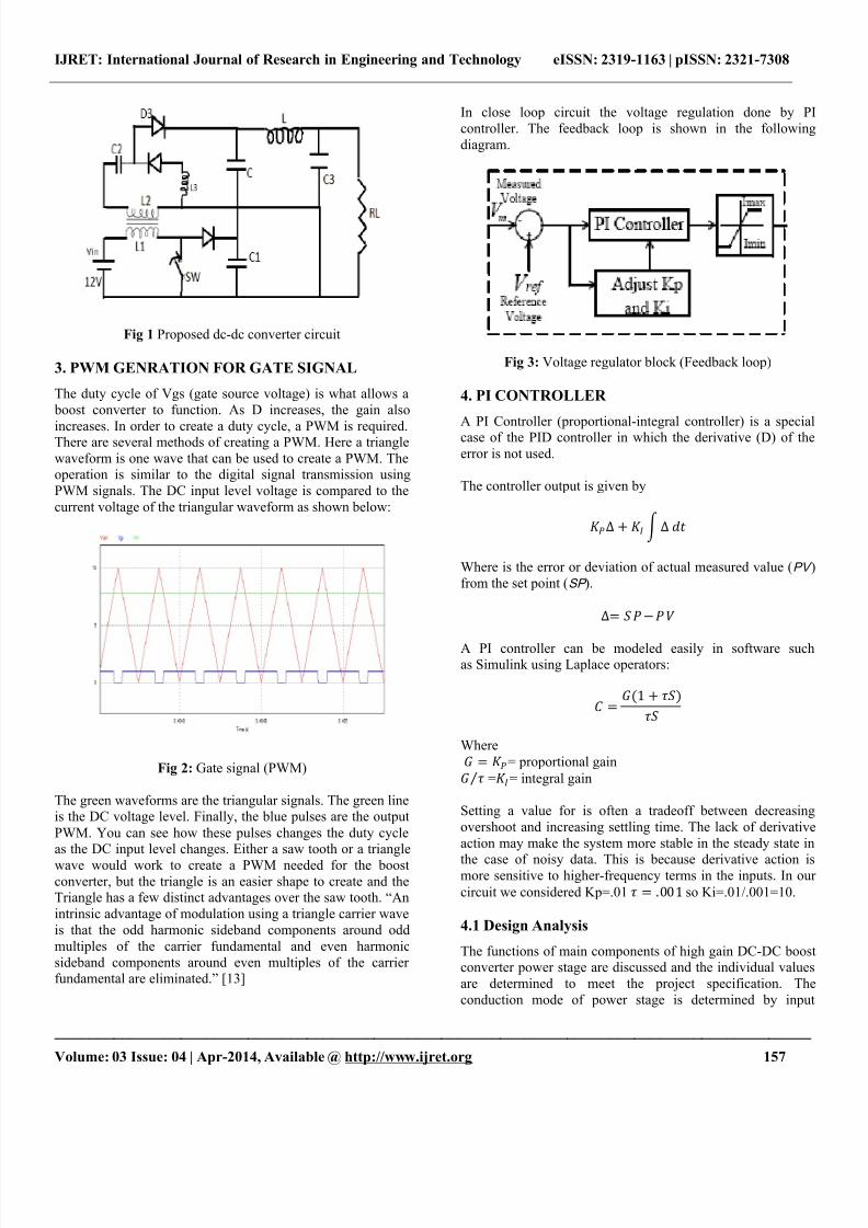
2. TOPOLOGY SELECTION
As we face several problem in the boost converters circuit likehigh reverse recovery current across the rectifier diode, turnON and turn OFF losses, the leakage inductance energy(which induces high voltage spikes across the active switch)and current stress in switching device. A solution for this is toreplace the boost input inductor by a coupled- inductorswitching cell formed by a transistor. The voltage stress on thetransistor was clamped by the output voltage. The rectifierdiode should also withstand the output voltage. In order toeven further reduce the current stresses on the switches, a newapproach is considered, where a current limiting inductorconnecting in the series with the secondary coil of the coupledinductor. Two diodes and a capacitor are added .The newconverter features a high conversion ratio, high gain combinedwith a small voltage stress on the switches. It keeps the softswitching operation of both active and passive switches, andthe alleviation of the recovery problem of the diodes.
The LC filter used to reduce ripple in the output voltage. Tomaintain output voltage constant and control the gate signalPI controller is used and the output voltage feed back to theinput.
8/12/2019 Design High Gain Dc-dc Boost Converter With Coupling Inductor and Simulation in Psim
http://slidepdf.com/reader/full/design-high-gain-dc-dc-boost-converter-with-coupling-inductor-and-simulation 2/8
IJRET: International Journal of Research in Engineering and Technology eISSN: 2319-1163 | pISSN: 2321-7308
__________________________________________________________________________________________
Volume: 03 Issue: 04 | Apr-2014, Available @ http://www.ijret.org 157
Fig 1 Proposed dc-dc converter circuit
3. PWM GENRATION FOR GATE SIGNAL
The duty cycle of Vgs (gate source voltage) is what allows a boost converter to function. As D increases, the gain also
increases. In order to create a duty cycle, a PWM is required.There are several methods of creating a PWM. Here a trianglewaveform is one wave that can be used to create a PWM. Theoperation is similar to the digital signal transmission usingPWM signals. The DC input level voltage is compared to thecurrent voltage of the triangular waveform as shown below:
Fig 2: Gate signal (PWM)
The green waveforms are the triangular signals. The green lineis the DC voltage level. Finally, the blue pulses are the outputPWM. You can see how these pulses changes the duty cycleas the DC input level changes. Either a saw tooth or a triangle
wave would work to create a PWM needed for the boostconverter, but the triangle is an easier shape to create and theTriangle has a few distinct advantages over the saw tooth. “An
intrinsic advantage of modulation using a triangle carrier waveis that the odd harmonic sideband components around oddmultiples of the carrier fundamental and even harmonicsideband components around even multiples of the carrierfundamental are eliminated.” [13]
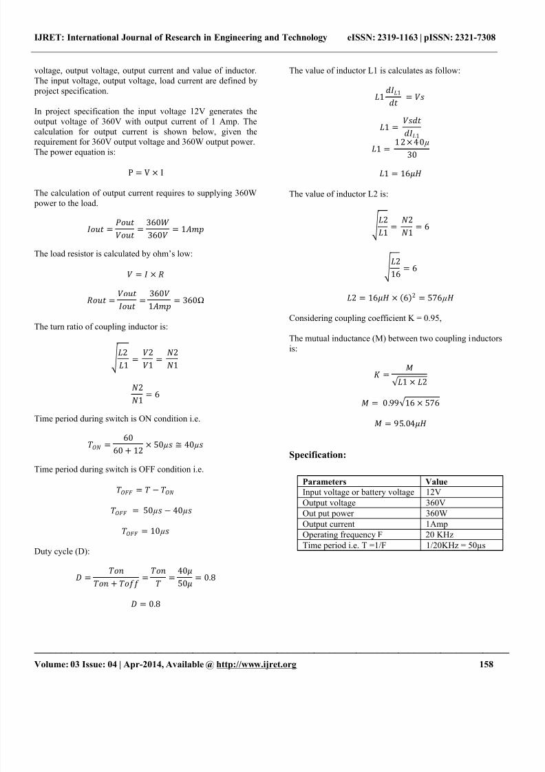
In close loop circuit the voltage regulation done by PIcontroller. The feedback loop is shown in the followingdiagram.
Fig 3: Voltage regulator block (Feedback loop)
4. PI CONTROLLER
A PI Controller (proportional-integral controller) is a specialcase of the PID controller in which the derivative (D) of theerror is not used.
The controller output is given by
∆ + ∆ Where is the error or deviation of actual measured value (PV from the set point (SP ).
∆= −
A PI controller can be modeled easily in software suchas Simulink using Laplace operators:
=(1 + )
Where = = proportional gain == integral gain
Setting a value for is often a tradeoff between decreasingovershoot and increasing settling time. The lack of derivativeaction may make the system more stable in the steady state in
the case of noisy data. This is because derivative action ismore sensitive to higher-frequency terms in the inputs. In our
circuit we considered Kp=.01 = .001 so Ki=.01/.001=10.
4.1 Design Analysis
The functions of main components of high gain DC-DC boosconverter power stage are discussed and the individual valuesare determined to meet the project specification. Theconduction mode of power stage is determined by input
8/12/2019 Design High Gain Dc-dc Boost Converter With Coupling Inductor and Simulation in Psim
http://slidepdf.com/reader/full/design-high-gain-dc-dc-boost-converter-with-coupling-inductor-and-simulation 3/8
IJRET: International Journal of Research in Engineering and Technology eISSN: 2319-1163 | pISSN: 2321-7308
__________________________________________________________________________________________
Volume: 03 Issue: 04 | Apr-2014, Available @ http://www.ijret.org 158
voltage, output voltage, output current and value of inductor.The input voltage, output voltage, load current are defined by project specification.
In project specification the input voltage 12V generates theoutput voltage of 360V with output current of 1 Amp. The
calculation for output current is shown below, given therequirement for 360V output voltage and 360W output power.The power equation is:
P = V × I
The calculation of output current requires to supplying 360W power to the load.
= =
360360 = 1
The load resistor is calculated by ohm’s low:
= ×
= =
3601 = 360Ω
The turn ratio of coupling inductor is:
21=
21=
21
2
1
= 6
Time period during switch is ON condition i.e.
=60
60 + 12× 50 µ ≅ 40 µ
Time period during switch is OFF condition i.e.
= −
= 50 µ − 40 µ
= 10 µ
Duty cycle (D):
= + =
=4050 = 0.8
= 0.8
The value of inductor L1 is calculates as follow:
11 =
1 =
1
1 =1 2 ×4 0 µ
30
1 = 16
The value of inductor L2 is:
21=
21= 6
2
16 = 6
2 = 16 × 62 = 576 µ
Considering coupling coefficient K = 0.95,
The mutual inductance (M) between two coupling inductorsis:
= 1 × 2
= 0.99 16 × 576 = 95.04
Specification:
Parameters Value
Input voltage or battery voltage 12V
Output voltage 360V
Out put power 360W
Output current 1Amp
Operating frequency F 20 KHz
Time period i.e. T =1/F 1/20KHz = 50µs
8/12/2019 Design High Gain Dc-dc Boost Converter With Coupling Inductor and Simulation in Psim
http://slidepdf.com/reader/full/design-high-gain-dc-dc-boost-converter-with-coupling-inductor-and-simulation 4/8
IJRET: International Journal of Research in Engineering and Technology eISSN: 2319-1163 | pISSN: 2321-7308
__________________________________________________________________________________________
Volume: 03 Issue: 04 | Apr-2014, Available @ http://www.ijret.org 159
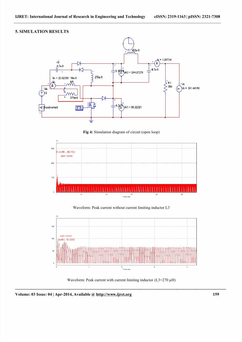
5. SIMULATION RESULTS
Fig 4: Simulation diagram of circuit (open loop)
Waveform: Peak current without current limiting inductor L3
Waveform: Peak current with current limiting inductor (L3=270 µH)

8/12/2019 Design High Gain Dc-dc Boost Converter With Coupling Inductor and Simulation in Psim
http://slidepdf.com/reader/full/design-high-gain-dc-dc-boost-converter-with-coupling-inductor-and-simulation 5/8
IJRET: International Journal of Research in Engineering and Technology eISSN: 2319-1163 | pISSN: 2321-7308
__________________________________________________________________________________________
Volume: 03 Issue: 04 | Apr-2014, Available @ http://www.ijret.org 160
Waveform: Inductor current (IL1)
Waveform: The output voltage (Vo) and inductor current (IL1)
Waveform: output voltage (Vo ) and output current (Io)
0.0144 0.0146 0.0148 0.015 0.0152 0.0154 0.0156 0.0158 0.016
Time (s)
0
-20
20
40
60
80
Iin

8/12/2019 Design High Gain Dc-dc Boost Converter With Coupling Inductor and Simulation in Psim
http://slidepdf.com/reader/full/design-high-gain-dc-dc-boost-converter-with-coupling-inductor-and-simulation 6/8
IJRET: International Journal of Research in Engineering and Technology eISSN: 2319-1163 | pISSN: 2321-7308
__________________________________________________________________________________________
Volume: 03 Issue: 04 | Apr-2014, Available @ http://www.ijret.org 161
In this circuit my main aim is to stabilized the output voltagewith better efficiency, remove the offset voltage and maintainthe limit of switching current.
Apart this simplified the controlling action. According thelimit of switching current we can able to select the switching
device and diode. The PI controller is used to stabilize theoutput of the circuit. The proportional gain Kp =0.01 and
integral gain Ki =10 and time constant =
0.001 1 .The simulation diagram of close loop circuiis shown below.
Fig 5: simulation diagram of circuit with feedback (close loop)
Waveform: output voltage (Vo) and output current (Io)

8/12/2019 Design High Gain Dc-dc Boost Converter With Coupling Inductor and Simulation in Psim
http://slidepdf.com/reader/full/design-high-gain-dc-dc-boost-converter-with-coupling-inductor-and-simulation 7/8
IJRET: International Journal of Research in Engineering and Technology eISSN: 2319-1163 | pISSN: 2321-7308
__________________________________________________________________________________________
Volume: 03 Issue: 04 | Apr-2014, Available @ http://www.ijret.org 162
Waveform: output voltage(Vo) and inductor current (IL1)
Waveform: Input current at full load condition
6. EFFICIENCY TESTING
The following efficiency testing was conducted in a closedloop configuration. The efficiency was calculated by the total power out divided by total power into the circuit.
Calculate the efficiency at full load condition by calculate theinput power and output power.
Efficiency in percentage =Output power
Input power × 100
At full load the output power = Vo * Io
Po = 360.3*1= 360.3W
Pin=Vin * Iin
Pin=12*31.1= 373.2W
Efficiency =360.3
373.3 × 100 = 96.5%
So we get better efficiency at full load condition that is 96.5%with control of switching peak current.
7. CONCLUSIONS
The boost converter is capable of operating at 20 KHz. The boost converter achieves a constant 360V output when it isexperiences at full load i.e. 360Ω and has voltage inputs o
12V. Furthermore, the boost converter minimized theswitching peak current from 266A to 90A by using currentlimiting inductor, alleviated the reverse recovery problem andachieve high step up voltage gain with duty cycle ratio of 0.8

8/12/2019 Design High Gain Dc-dc Boost Converter With Coupling Inductor and Simulation in Psim
http://slidepdf.com/reader/full/design-high-gain-dc-dc-boost-converter-with-coupling-inductor-and-simulation 8/8