Design Guidelines for 100 Gbps - CFP2 Interface · optical module that uses CEI-28G-VSR as its...
15
Design Guidelines for 100 Gbps - CFP2 Interface 2014.01.16 AN-684 Subscribe Send Feedback is document shows an example layout design that implements a 4 x 25/28 Gbps CFP2 module interface that meets the insertion and return loss mask requirements proposed in the working clause draſt version 8.0 for CEI-28G-VSR. e common electrical interface CEI-28G-VSR implementation architecture (IA) for short reach channels is intended for next generation 100 Gbps chip - to - optical module applications. CFP2 is a pluggable optical module that uses CEI-28G-VSR as its electrical interface (as defined by the CFP Multi-Source Agreement (MSA) member companies). CFP2 also defines the mechanical form factor for a 100 Gbps optical transceiver module targeted for Ethernet and OTN (Optical Transport Network) applications. CFP2 provides an industry standard to develop next generation 100 G interfaces with lower power and greater port density compared to previous generation CFP optical modules. Note: For more information, refer to the CEI-28G-VSR working clause specification. Document number OIF2010.404.08. Figure 1: Stratix V GT Device to a CFP2 Pluggable Module Interface on a PCB Stratix V GT Device PCB Material GND Reference Plane Egress Ingress TX and RX Breakout Transceiver Serial Link Module Cage Module Connector CFP2 Pluggable Module Backdrilled Vias Backdrilled Vias e channel layout on the PCB is optimized in order to meet the strict insertion and return loss masks defined by CEI-28G-VSR. Refer to the following documents for more information on optimizing your board designs for high speed serial links. Related Information • AN529: Via Optimization Techniques for High-Speed Channel Designs • AN530: Optimizing Impedance Discontinuity Caused by Surface Mount Pads for High-Speed Channel Designs Intel Corporation. All rights reserved. Intel, the Intel logo, Altera, Arria, Cyclone, Enpirion, MAX, Nios, Quartus and Stratix words and logos are trademarks of Intel Corporation or its subsidiaries in the U.S. and/or other countries. Intel warrants performance of its FPGA and semiconductor products to current specifications in accordance with Intel's standard warranty, but reserves the right to make changes to any products and services at any time without notice. Intel assumes no responsibility or liability arising out of the application or use of any information, product, or service described herein except as expressly agreed to in writing by Intel. Intel customers are advised to obtain the latest version of device specifications before relying on any published information and before placing orders for products or services. *Other names and brands may be claimed as the property of others. ISO 9001:2015 Registered www.altera.com 101 Innovation Drive, San Jose, CA 95134
Transcript of Design Guidelines for 100 Gbps - CFP2 Interface · optical module that uses CEI-28G-VSR as its...
Design Guidelines for 100 Gbps - CFP2 Interface2014.01.16
AN-684 Subscribe Send Feedback
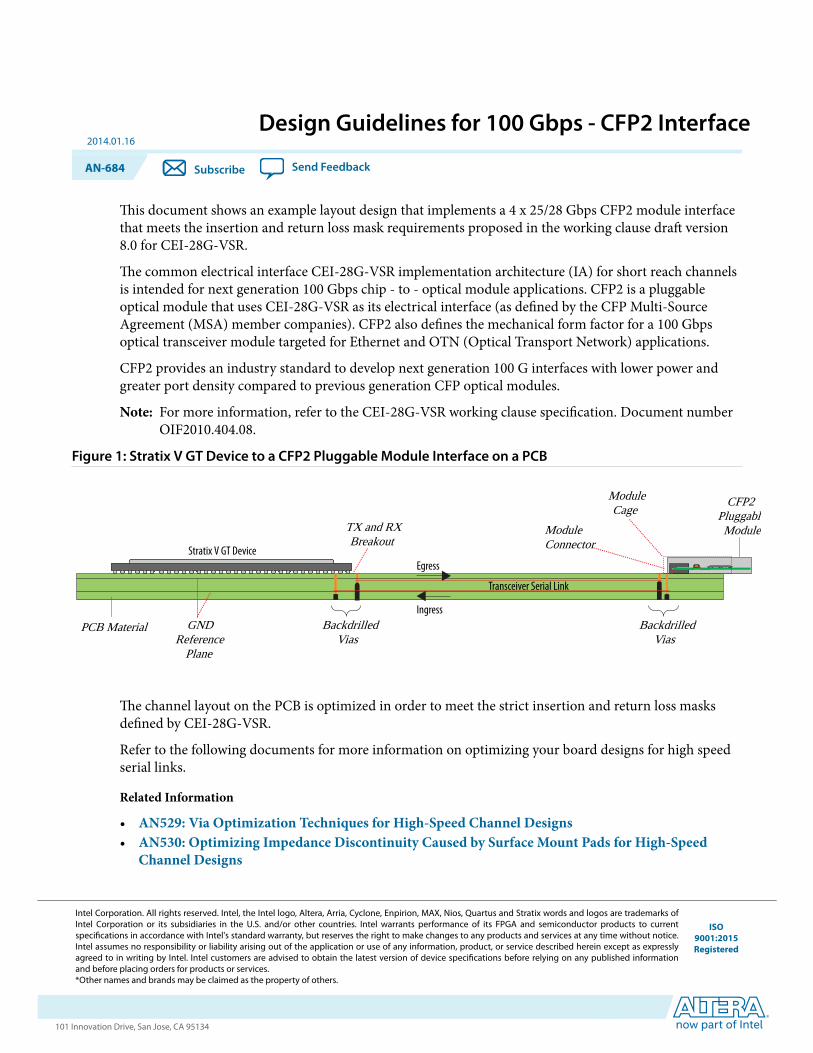
This document shows an example layout design that implements a 4 x 25/28 Gbps CFP2 module interfacethat meets the insertion and return loss mask requirements proposed in the working clause draft version8.0 for CEI-28G-VSR.
The common electrical interface CEI-28G-VSR implementation architecture (IA) for short reach channelsis intended for next generation 100 Gbps chip - to - optical module applications. CFP2 is a pluggableoptical module that uses CEI-28G-VSR as its electrical interface (as defined by the CFP Multi-SourceAgreement (MSA) member companies). CFP2 also defines the mechanical form factor for a 100 Gbpsoptical transceiver module targeted for Ethernet and OTN (Optical Transport Network) applications.
CFP2 provides an industry standard to develop next generation 100 G interfaces with lower power andgreater port density compared to previous generation CFP optical modules.
Note: For more information, refer to the CEI-28G-VSR working clause specification. Document numberOIF2010.404.08.
Figure 1: Stratix V GT Device to a CFP2 Pluggable Module Interface on a PCB
Stratix V GT Device
PCB Material GNDReference
Plane
Egress
Ingress
TX and RXBreakout
Transceiver Serial Link
ModuleCage
ModuleConnector
CFP2PluggableModule
BackdrilledVias
BackdrilledVias
The channel layout on the PCB is optimized in order to meet the strict insertion and return loss masksdefined by CEI-28G-VSR.
Refer to the following documents for more information on optimizing your board designs for high speedserial links.
Related Information
• AN529: Via Optimization Techniques for High-Speed Channel Designs• AN530: Optimizing Impedance Discontinuity Caused by Surface Mount Pads for High-Speed
Channel Designs
Intel Corporation. All rights reserved. Intel, the Intel logo, Altera, Arria, Cyclone, Enpirion, MAX, Nios, Quartus and Stratix words and logos are trademarks ofIntel Corporation or its subsidiaries in the U.S. and/or other countries. Intel warrants performance of its FPGA and semiconductor products to currentspecifications in accordance with Intel's standard warranty, but reserves the right to make changes to any products and services at any time without notice.Intel assumes no responsibility or liability arising out of the application or use of any information, product, or service described herein except as expresslyagreed to in writing by Intel. Intel customers are advised to obtain the latest version of device specifications before relying on any published informationand before placing orders for products or services.*Other names and brands may be claimed as the property of others.
ISO9001:2015Registered
www.altera.com101 Innovation Drive, San Jose, CA 95134

Stratix V GT Transceiver ChannelsStratix® V GT FPGAs offer four transceiver channels (ATT_TXR[3:0]_P/N and ATT_RXR[3:0]_P/N) thatcan operate up to 28 Gbps for interfacing with CFP2 or other optical modules.
Figure 2: Top View of 28 Gbps Transmitter and Receiver Channel Locations in Stratix V GT FPGAs
AWAVAUATARAPANAMALAKAJAHAGAFAEADACABAAYWVUTRPNMLKJHGFEDCBA
ATT_TXRN_0ATT_TXRP_0ATT_RXRN_0ATT_RXRP_0
ATT_TXRN_1ATT_TXRP_1ATT_RXRN_1ATT_RXRP_1
ATT_TXRN_2ATT_TXRP_2ATT_RXRN_2ATT_RXRP_2
ATT_TXRN_3ATT_TXRP_3ATT_RXRN_3ATT_RXRP_3
39 35 30 25 20 15 10 5 1
CFP2 Host Connector Assembly and PinoutThe CFP2 specification defines the mechanical connector requirements for the 104-pin CFP2 connector.The host connector assembly is composed of a female host connector, and a metal connector cover andcage for retention and electromagnetic shielding of the inserted CFP2 optical module.
2 Stratix V GT Transceiver ChannelsAN-684
2014.01.16
Altera Corporation Design Guidelines for 100 Gbps - CFP2 Interface
Send Feedback
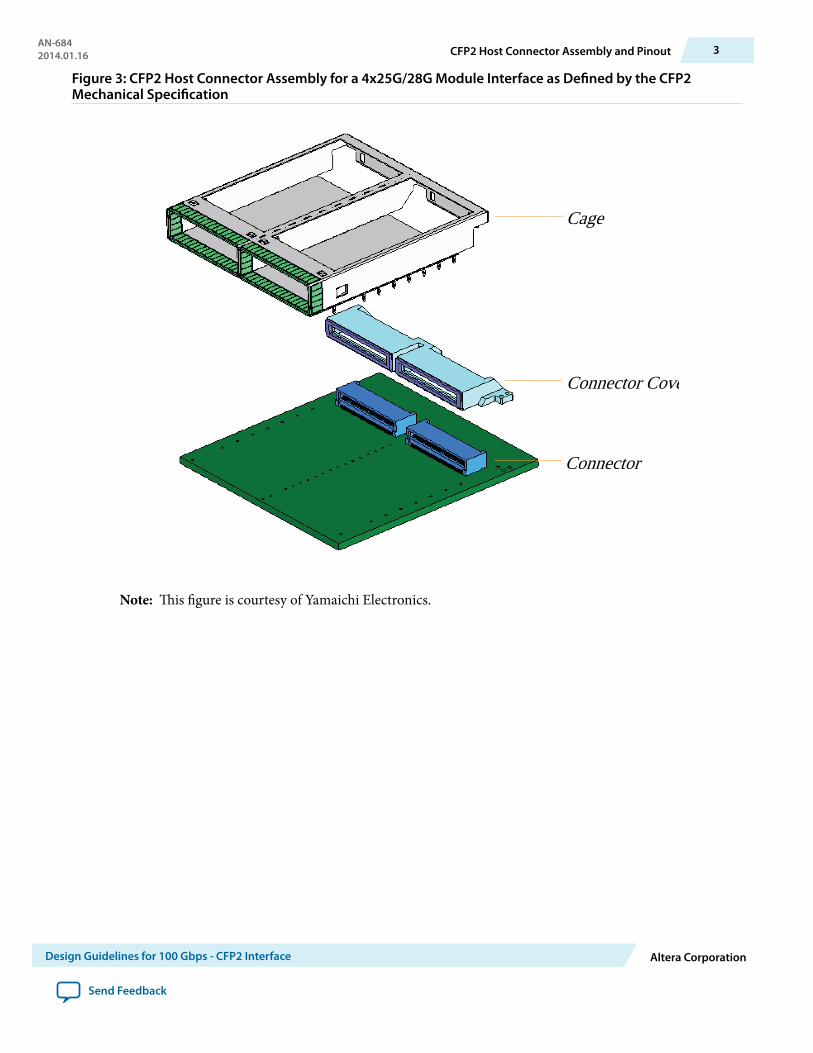
Figure 3: CFP2 Host Connector Assembly for a 4x25G/28G Module Interface as Defined by the CFP2Mechanical Specification
Cage
Connector Cover
Connector
Note: This figure is courtesy of Yamaichi Electronics.
AN-6842014.01.16 CFP2 Host Connector Assembly and Pinout 3
Design Guidelines for 100 Gbps - CFP2 Interface Altera Corporation
Send Feedback

Figure 4: CFP2 Host Connector Pinout for 4x25G/28G Module Interface as Defined by the CFP2 MechanicalSpecification
4 CFP2 Host Connector Assembly and PinoutAN-684
2014.01.16
Altera Corporation Design Guidelines for 100 Gbps - CFP2 Interface
Send Feedback

Figure 5: CFP2 Host Connector Layout FootprintThe high-speed transceiver pins are identified in the following figure to show their position within theconnector. Blue pins are the TX transceiver channels and red pins are the RX transceiver channels.
5355
60
65
70
75
80
85
90
95
100
104
50
45
40
35
30
25
20
15
10
5
1
RX0pRX0nRX1pRX1nRX2pRX2nRX3pRX3n
TX0pTX0nTX1pTX1nTX2pTX2nTX3pTX3n
Stratix V GT to CFP2 Interface Layout DesignThe TX and RX channels are connected directly to the CFP2 connector with approximately 5.5 inches ofdifferential trace routing on the top and bottom layer of the board. DC blocking capacitors are included inthe optical module for both the TX and RX traces. Nominal trace impedance is controlled at approxi‐mately 100Ω differential and the board material used is Panasonic Megtron-6.
AN-6842014.01.16 Stratix V GT to CFP2 Interface Layout Design 5
Design Guidelines for 100 Gbps - CFP2 Interface Altera Corporation
Send Feedback

Figure 6: Stratix V GT to CFP2 Interface Layout Design Example
The figure shows an example layout design where the green traces are the TX channels routed on the toplayer while the orange traces are the RX channels routed on the bottom layer.
RX0RX1RX2
RX3
TX0
TX1TX2
TX3
CFP2 ConnectorCover Keepout
CFP2 ConnectorTX Signals ChangingLayer to Avoid CFP2
Metal Connector Cover
Channel Routing
Stratix V GT BGA
In this example, vias are used for the RX channel breakout at the BGA, and for both the TX and RXchannels at the CFP2 connector. To avoid the top layer keep out requirement of the CFP2 metal connectorcover assembly, the TX channel routing is switched briefly to the bottom layer and then back to the toplayer at the CFP2 connector as illustrated by the circled area in the above figure. Top to bottom routing isused to avoid via stubs.
The BGA pads, signal vias, and CFP2 trace to pad interfaces are large discontinuity sources in the channel.Ansys HFSS (High Frequency Structural Simulator) 3-D field solver simulation is used to optimize theBGA breakout and CFP2 interface design. The trace impedance is kept within ±10% of the nominal 100Ω
Board Stack Up DimensionsThe detailed trace design and board stack up dimensions are shown in the figure below.
6 Board Stack Up DimensionsAN-684
2014.01.16
Altera Corporation Design Guidelines for 100 Gbps - CFP2 Interface
Send Feedback
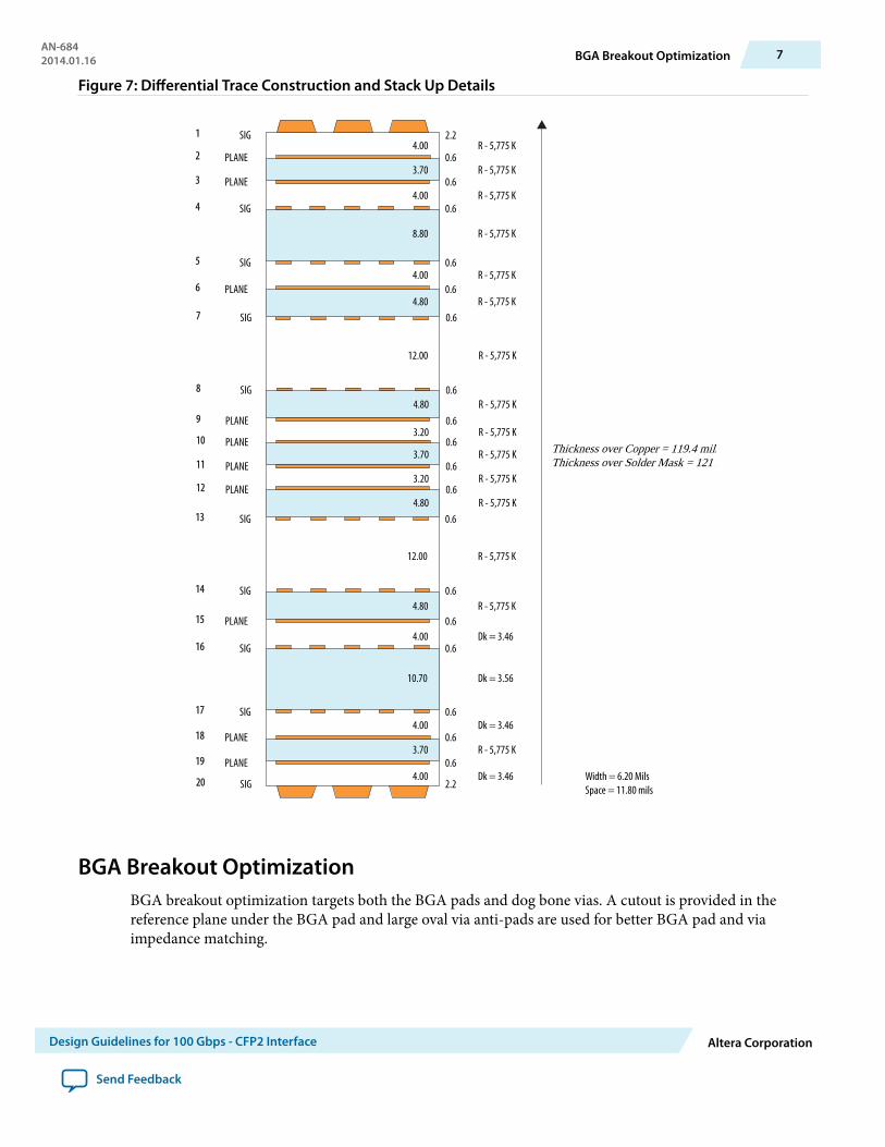
Figure 7: Differential Trace Construction and Stack Up Details
4.00
3.70
4.00
8.80
4.00
4.80
12.00
4.80
3.20
3.70
3.20
4.80
12.00
4.80
4.00
10.70
4.00
4.00
3.70
SIG
PLANE
PLANE
SIG
SIG
PLANE
SIG
SIG
PLANE
PLANE
PLANE
PLANE
SIG
SIG
PLANE
SIG
SIG
PLANE
PLANE
2.2
0.6
0.6
0.6
0.6
0.6
0.6
0.6
0.6
0.6
0.6
0.6
0.6
0.6
0.6
0.6
0.6
0.6
0.6
R - 5,775 K
R - 5,775 K
R - 5,775 K
R - 5,775 K
R - 5,775 K
R - 5,775 K
R - 5,775 K
R - 5,775 K
R - 5,775 K
R - 5,775 K
R - 5,775 K
R - 5,775 K
R - 5,775 K
R - 5,775 K
Dk = 3.46
Dk = 3.56
Dk = 3.46
Dk = 3.46
R - 5,775 K
Thickness over Copper = 119.4 milsThickness over Solder Mask = 121 mils
Width = 6.20 MilsSpace = 11.80 milsSIG 2.2
1
2
3
4
5
6
7
8
9
10
11
12
13
14
15
16
17
19
18
20
BGA Breakout OptimizationBGA breakout optimization targets both the BGA pads and dog bone vias. A cutout is provided in thereference plane under the BGA pad and large oval via anti-pads are used for better BGA pad and viaimpedance matching.
AN-6842014.01.16 BGA Breakout Optimization 7
Design Guidelines for 100 Gbps - CFP2 Interface Altera Corporation
Send Feedback

Figure 8: BGA Via Breakout Layout Optimization
TX ChannelCutout underBGA Pad
RX Channel
Oval Via Anti-Pad
8 BGA Breakout OptimizationAN-684
2014.01.16
Altera Corporation Design Guidelines for 100 Gbps - CFP2 Interface
Send Feedback

Figure 9: TDR of BGA Via Breakout
HFSS simulation results show that the TDR deviation of the BGA escape is maintained within ±10% of thenominal 100Ω channel target impedance.
CFP2 Interface OptimizationThe CFP2 host connector layout optimization reduces the impact of discontinuity at the differential pair tothe CFP2 connector interface. A reference plane cutout is provided beneath the connector pads and largeroval anti-pads are used for the signal vias. Four nearby ground return vias are provided to help reduce theconnector interface discontinuity.
AN-6842014.01.16 CFP2 Interface Optimization 9
Design Guidelines for 100 Gbps - CFP2 Interface Altera Corporation
Send Feedback
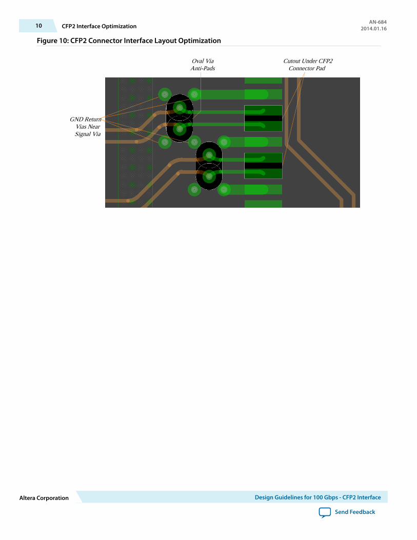
Figure 10: CFP2 Connector Interface Layout Optimization
GND ReturnVias NearSignal Via
Oval ViaAnti-Pads
Cutout Under CFP2Connector Pad
10 CFP2 Interface OptimizationAN-684
2014.01.16
Altera Corporation Design Guidelines for 100 Gbps - CFP2 Interface
Send Feedback

Figure 11: HFSS Simulated TDR of the CFP2 Connector interface
The following figure shows the HFSS simulated TDR results. With the layout optimizations, the TDRdeviation due to the discontinuity caused by the via and connector pad is kept within ±10% of the nominal100Ω target impedance.
Example Design Channel PerformanceThe CEI-28G-VSR working clause defines several mask requirements for the channel, including insertionloss, return loss, and differential-to-common mode conversion. Because it is difficult to verify electricalparameters of a full channel in a system, the working clause also defines a Host Compliance Board (HCB)with test points for verifying the host-to-module channel performance at various test points.
AN-6842014.01.16 Example Design Channel Performance 11
Design Guidelines for 100 Gbps - CFP2 Interface Altera Corporation
Send Feedback

Figure 12: Host Compliance Board Measurement Points
Host-to-ModuleTransmit Function
Host-to-ModuleReceive Function
TPOHost PCB Trace
TPOa
Host Channel
HCB PCB
Trace
TP1a
TP4a
For example, TP1a and TP4a define the measurement points and the associated mask requirements for thehost-to-module electrical signal performance for insertion loss, return loss, and differential-to-commonmode conversion. For more information about these definitions, refer to the CEI-28G-VSR working clausespecification (document number OIF2010.404.08).
Simulation Results for Stratix V GT to CFP2 Connector Layout DesignAnsys HFSS (High Frequency Structural Simulator) simulation results for the insertion loss (SDD21),return loss (SDD11) and differential-to-common mode conversion (SDC11) of the channel with the CFP2connector included are shown in the following figures. The simulation models the HCB for validating thechannel layout against the CEI-28G-VSR defined masks.
12 Simulation Results for Stratix V GT to CFP2 Connector Layout DesignAN-684
2014.01.16
Altera Corporation Design Guidelines for 100 Gbps - CFP2 Interface
Send Feedback

Figure 13: Insertion Loss versus CEI-28G-VSR Mask Requirements
The SDD21 resides within the HCB minimum and maximum insertion loss masks as defined by theCEI-28G-VSR specification. This insertion loss meets the complete VSR channel (host board + connector+ optical module) mask requirement with ample margin to accommodate the additional loss of aninserted CFP2 optical module. Note that the complete channel with the optical module is not simulated.
Similarly, the figures below show that the return loss and differential-to-common mode conversion bothmeet their respective masks as defined by the CEI-28G-VSR requirement.
AN-6842014.01.16 Simulation Results for Stratix V GT to CFP2 Connector Layout Design 13
Design Guidelines for 100 Gbps - CFP2 Interface Altera Corporation
Send Feedback
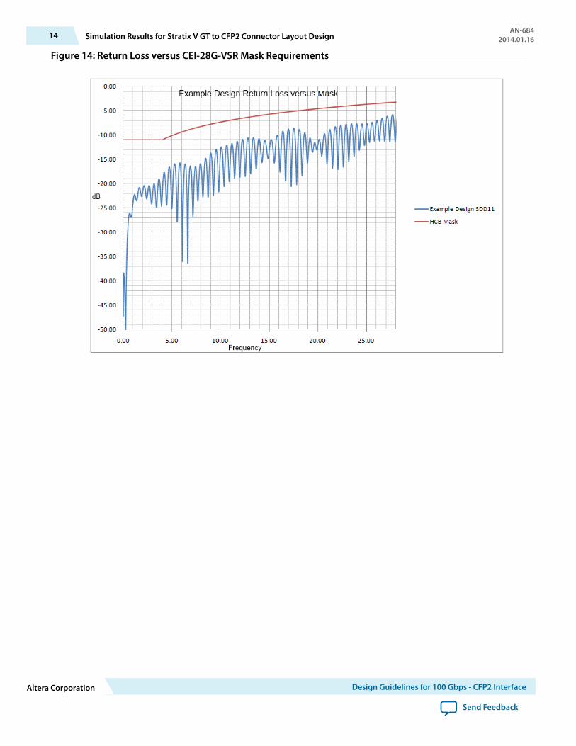
Figure 14: Return Loss versus CEI-28G-VSR Mask Requirements
14 Simulation Results for Stratix V GT to CFP2 Connector Layout DesignAN-684
2014.01.16
Altera Corporation Design Guidelines for 100 Gbps - CFP2 Interface
Send Feedback

Figure 15: Mode Conversion versus CEI-28G-VSR Mask Requirements
Document Revision History
Table 1: Document Revision History
Date Version Changes
January 2014 2014.01.16 • Changed "Ansoft HFSS" to "Ansys HFSS".• Updated HFSS definition to High Frequency
Structural Simulator.• Updated Simulation Results for Stratix V GT to CFP2
Connector Layout section to clarify that HFSS is usedfor the simulation.
March 2013 2013.03.29 Initial release.
AN-6842014.01.16 Document Revision History 15
Design Guidelines for 100 Gbps - CFP2 Interface Altera Corporation
Send Feedback