Design, Fabrication and Characterization of Passive and Active
160
Design, Fabrication and Characterization of Passive and Active Polymer Photonic Devices Geetha K International School of Photonics Cochin University of Science and Technology Cochin – 682 022, India Ph D Thesis submitted to Cochin University of Science and Technology In partial fulfillment of the requirements for the Degree of Doctor of Philosophy June, 2006
Transcript of Design, Fabrication and Characterization of Passive and Active

Design, Fabrication and Characterization of
Passive and Active Polymer Photonic Devices
Geetha K
International School of Photonics Cochin University of Science and Technology
Cochin – 682 022, India
Ph D Thesis submitted to Cochin University of Science and Technology
In partial fulfillment of the requirements for the Degree of Doctor of Philosophy
June, 2006

Design, Fabrication and Characterization of Passive and Active Polymer Photonic Devices Ph D Thesis in the filed of Photonics Author Geetha K Research Fellow International School of Photonics Cochin University of Science & Technology Cochin – 682 022, India Email : [email protected]; [email protected] Research Advisors Dr. P Radhakrishnan Professor, International School of Photonics Cochin University of Science & Technology Cochin – 682 022, India Email : [email protected] Dr. V P N Nampoori Professor, International School of Photonics Cochin University of Science & Technology Cochin – 682 022, India Email : [email protected] International School of Photonics, Cochin University of Science & Technology Cochin – 682 022, INDIA www.photonics.cusat.edu June 2006 Front cover : Multimode laser emission from a 50 µm thick polymer planar waveguide doped with Rhodamine 6G

�
�
������������
���� �����������

CERTIFICATE
Certified that the research work presented in the thesis entitled
“Design, fabrication and characterization of passive and active
polymer photonic devices” is based on the original work done by
Mrs. Geetha K under my guidance and supervision at the International
School of Photonics, Cochin University of Science and Technology,
Cochin – 22, India and has not been included in any other thesis
submitted previously for the award of any degree.
Cochin 682 022 Dr. P Radhakrishnan
1 June, 2006 (Supervising Guide)

DECLARATION
Certified that the work presented in the thesis entitled “Design,
fabrication and characterization of passive and active polymer
photonic devices ” is based on the original work done by me under the
guidance and supervision of Dr. P Radhakrishnan, Professor,
International School of Photonics, Cochin University of Science and
Technology, Cochin – 22, India and co-guidance of Dr. V P N
Nampoori, Professor, International School of Photonics, Cochin
University of Science and Technology, Cochin – 22, India and has not
been included in any other thesis submitted previously for the award of
any degree.
Cochin 682 022
1 June, 2006 Geetha K

Preface
The rapid developments in fields such as fibre optic communication
engineering and integrated optical electronics have expanded the interest and
have increased the expectations about guided wave optics, in which optical
waveguides and optical fibres play a central role. The technology of guided
wave photonics now plays a role in generating information (guided-wave
sensors) and processing information (spectral analysis, analog-to-digital
conversion and other optical communication schemes) in addition to its
original application of transmitting information (fibre optic communication).
Passive and active polymer devices have generated much research
interest recently because of the versatility of the fabrication techniques and
the potential applications in two important areas – short distant
communication network and special functionality optical devices such as
amplifiers, switches and sensors. Polymer optical waveguides and fibres are
often designed to have large cores with 10-1000 micrometer diameter to
facilitate easy connection and splicing.
Large diameter polymer optical fibres being less fragile and vastly
easier to work with than glass fibres, are attractive in sensing applications.
Sensors using commercial plastic optical fibres are based on ideas already
used in silica glass sensors, but exploiting the flexible and cost effective
nature of the plastic optical fibre for harsh environments and throw-away
sensors.
In the field of Photonics, considerable attention is centering on the
use of polymer waveguides and fibres, as they have a great potential to create
all-optical devices. By attaching organic dyes to the polymer system we can
incorporate a variety of optical functions. Organic dye doped polymer
waveguides and fibres are potential candidates for solid state gain media.

High power and high gain optical amplification in organic dye-doped
polymer waveguide amplifier is possible due to extremely large emission
cross sections of dyes. Also, an extensive choice of organic dye dopants is
possible resulting in amplification covering a wide range in the visible region.
The thesis presented in seven chapters deals with the work carried
out on polymer optical fibre sensors and dye doped polymer waveguide gain
media.
Chapter 1 gives an overview of guided wave polymer photonic devices.
Historical development of polymer waveguides/fibres and commonly used
polymer materials together with their applications have been covered. An
overview of passive components with emphasis on polymer fibre optic
sensors and different sensing techniques is given. The potential of polymer
waveguides and fibres as optically active media is also discussed. Recent
developments in the related fields such as conjugated polymer devices and
polymer photonic band gap materials have also been mentioned.
Chapter 2 discusses the design, fabrication and characterization of a
refractometer using a side polished polymer fibre, which has got a wide
dynamic range. Following a ray optics approach to multimode fibres, a
theoretical model was developed for understanding the sensor performance
for various launching angles to the fibre. Based on the theoretical
observations, the experiment was designed. The sensing element was
fabricated by encapsulating a slightly bent polymer optical fibre in a block
of resin. Maximum sensitivity and sensing range was obtained for a
launching angle of 300. The experimental results are explained on the basis
of theoretical calculations.
Chapter 3 presents an evanescent wave absorption sensor for chemical
reaction rate measurements. General theory of evanescent wave absorption
in fibres is overviewed. A theoretical study of the effect of a high refractive
index overlay on the exposed core region of the fibre, on the evanescent
wave absorption is presented. Details of the modeling related to the
evanescent wave absorption for different overlay refractive indices and
overlay thicknesses are also included in this chapter. It was observed that the
evanescent wave absorption coefficient increases with increase in overlay
refractive index and overlay thickness. Experiments were also performed for
studying the reaction kinetics of a standard chemical reaction. Experimental
results for bare fibre as well as fibres with different overlay thickness are also
presented in this chapter .
Chapter 4 gives the details of the fabrication and characterization of dye
doped polymer planar waveguide structures. Rhodamine 6G doped
polymethyl methacrylate (PMMA) planar film waveguides with various dye
concentrations and thicknesses were prepared by tape casting technique. The
optical attenuation in the waveguides is an important parameter of interest.
The loss characterization was done by a non-destructive side illumination
fluorescence technique, the details of which are presented in this chapter. The
experimental results for waveguides with various dye concentration and
thickness are discussed in this chapter. The studies showed that the
attenuation mechanisms in a dye doped waveguide – especially for the dyes
having an overlap between the absorption and emission spectra – can be
explained only with a space dependent attenuation coefficient. In such cases,
the transmitted light will not strictly obey the conventional Beer-Lambert’s
law.

In Chapter 5, the observation of Amplified Spontaneous Emission (ASE)
from the dye doped planar waveguide structures of various thicknesses and
dye concentrations has been presented. Optical gain characterization was
done by a variable stripe length method widely used for both organic and
inorganic materials prepared in slab geometry. The cross-section of the pump
beam was in the form of a stripe. The variation of gain with dye
concentration as well as film thickness has been studied. The propagation
characteristics of ASE through the waveguide are also discussed. This was
done by shifting the position of the excitation stripe in such a way that the
ASE from the end of the pump stripe was guided along different lengths of
the waveguide. With increase in propagation length through the waveguide,
the emission peak showed a red-shift due to self-absorption and re-emission
by the dye molecules. As the radiation was propagated through the
amplifying medium, a spectrally narrow output at longer wavelengths was
obtained due to the gain achieved at these wavelengths. Thus we could tune
the ASE wavelength.
Chapter 6 describes the details of our work on multimode laser emission
from a transversely pumped free standing polymer film of Rh6G doped
PMMA . Since the film was freestanding – surrounded by air on both sides
– the reflections from the lateral faces of the sample provided the optical
feedback for laser action. This was evident from the lasing mode-spacing
dependence on the film thickness. The leaky mode emission from the film
waveguide showed a planar microcavity-like behaviour due to Fabry-Perot
effects. Selective mode excitation was also observed with an increase in
pump energy.
Summary and conclusions of the work carried out are given in Chapter 7.
Future prospects are also discussed in this chapter.

List of Publications
International Journals
1. K. Geetha, M. Rajesh, V.P.N. Nampoori, C.P.G. Vallabhan and P.Radhakrishnan, “Propagation characteristics and wavelength tuning of amplified spontaneous emission from dye doped polymer”, Appl. Opt. 45, 764-769 (2006)
2. K. Geetha, M. Rajesh, V.P.N. Nampoori, C.P.G. Vallabhan and
P.Radhakrishnan, “Laser emission from transversely pumped dye-doped free-standing polymer film”, J.Opt. A: Pure Appl. Opt. 8,189-193 (2006)
3. K. Geetha, M. Rajesh, V.P.N. Nampoori, C.P.G. Vallabhan and
P.Radhakrishnan, “Loss characterization in rhodamine 6G doped polymer film waveguide by side illumination fluorescence”, J.Opt. A: Pure Appl. Opt. 6, 379-383 (2004).
4. K. Geetha, Pramod Gopinath, K P Unnikrishnan, S Thomas Lee ,C.
P. G. Vallabhan,V. P. N. Nampoori and P. Radhakrishnan, “Studies on optical loss coefficient in plastic waveguides”, Proceedings of SPIE – International Society of optical Engineering, No. 4904, 382-390 (2002).
5. M Rajesh, K Geetha, M. Sheeba, P Radhakrishnan, C P G Vallabhan
and V P N Nampoori, “Characterization of Rhodamine 6G doped polymer optical fiber by side illumination fluorescence”, Optical Engg (In Press)
6. M. Rajesh, K. Geetha, M. Sheeba, P. Radhakrishnan, C. P. G
Vallabhan and V. P. N Nampoori, “A fiber optic smart sensor for studying the setting characteristics of various grades of cement”, Optics and lasers in Engineering 44, 486-493 (2006)
7. S. Thomas Lee, K. Geetha, V.P.N. Nampoori, C.P.G. Vallabhan and
P. Radhakrishnan, “ Microbent Optical fibers as evanescent wave sensors”, Opt. Engg. 41, 3260-3264 (2002).
8. K. Geetha, M. Rajesh, V. P. N. Nampoori and P. Radhakrishnan, “A
modified design of refractometer using side polished polymer fibre”. (Communicated to Optical and Quantum Electronics)

International Conferences
1. K. Geetha, M. Rajesh, C.P.G. Vallabhan , V.P.N. Nampoori and P.Radhakrishnan, “Design of a refractometer with wide dynamic range using side polished polymer optical fibre”, Proceedings of Seventh International Conference on Optoelectronics, Fiber Optics and Photonics ( PHOTONICS 2004) Dec 9-11, Kochi (2004)
2. K. Geetha, T. Anto Johny, V. Kumar, C.P.G. Vallabhan, V.P.N.
Nampoori and P.Radhakrishnan, “Modes in planar waveguides based on sol-gel derived thin films of nano ZnO”, Proceedings of Sixth International Conference on Optoelectronics, Fiber Optics and Photonics (PHOTONICS 2002), Dec 14-16,Mumbai(2002)
3. M. Rajesh, M. Sheeba, K. Geetha, P. Radhakrishnan, C.P.G.
Vallabhan and V.P.N. Nampoori, “A Fiber optic distributed sensor to characterize the properties of concrete mix”, Proceedings of Seventh International Conference on Optoelectronics, Fiber Optics and Photonics ( PHOTONICS 2004) Dec 9-11, Kochi (2004)
4. M. Rajesh, M. Sheeba, K. Geetha, P. Radhakrishnan, C.P.G.
Vallabhan and V.P.N. Nampoori, “Fiber optic sensor for the detection of paraffin oil traces in coconut oil”, Proceedings of Seventh International Conference on Optoelectronics, Fiber Optics and Photonics ( PHOTONICS 2004) Dec 9-11, Kochi (2004)
National Conferences 1. K. Geetha, M. Rajesh,V. P. N. Nampoori, C.P.G. Vallabhan and
P. Radhakrishnan, “Side Illumination Fluorescence Technique for the characterisation of optical loss in Dye doped planar waveguides”, National Laser Symposium 2003, Kharagpur
1. K. Geetha, Pramod Gopinath, K. P. Unnikrishnan, S. Thomas Lee,
C. P. G. Vallabhan,V. P. N. Nampoori and P. Radhakrishnan, “Side Illumination Fluorescence Studies in Dye doped Polymer Waveguide”, Proceedings of National Laser Symposium 2001, December 19-21, CAT Indore, pp141-142. (2001)

ACKNOWLEDGEMENTS With deep sense of gratitude, I express my heartfelt thanks to Prof. P. Radhakrishnan for the guidance, support and encouragement given through out my research work. I am extremely thankful to Prof. V. P. N. Nampoori for the inspiration, guidance and encouragement without which this work would not have materialized. I sincerely thank Prof. C.P.Girijavallabhan for his help and support. His valuable suggestions have helped me a lot in my research work. I am equally thankful to Prof. V.M. Nandakumaran for the timely help and encouragement. I also acknowledge Mr. M. Kailasnath. I am very much indebted to Dr. Reghu Natarajan, C-MET, Thrissur and Mr. Denny Alapatt, for providing me with the samples. I am also grateful to Dr. Rani Joseph, Dept. of Polymer Science and Rubber Technology, Cusat, who devoted her precious time for meaningful discussions. I owe much to Dr. A. Deepthy for the moral support and timely advices. I am thankful to all research scholars of ISP for their constant support and priceless help. I am extremely thankful to Rajesh M whose timely support helped me a lot in completing my work. The help rendered by Manoj Mathew is also worth mentioning . I remember the wonderful moments with Pramod, Sajan, Binoy, Unni, Prasanth, Pravitha, Jyotsna, Bindu, Aneesh ,Thomas Lee, Rajesh S, Rekha, Santhi, Dilna, Sreeja and Suresh Sir. I have also enjoyed the motherly affection from Achamma teacher. The love and support from Sr. Ritty is greatly acknowledged. I am thankful to all my friends - Sheeba, Thomas, Litty, Lyjo, Dann, Manu, Vinu, Sajeev, Parvathy, Saritha, Jayasree teacher and Bindu Krishnan. I am extremely thankful to Jijo, who helped me a lot in designing the cover page. .

I extend my sincere thanks to the non-teaching staff of ISP for all the help and assistance. The financial assistance from CSIR, India is greatly acknowledged. In this moment, I would like to remember all my friends especially Deepa Chandran, Grace, Vinod, Majo, Binu, Saritha and Jalaja who always encouraged me and supported me. I am extremely grateful to my brother and all my relatives. Their love and support have always been there. I also remember with gratitude the help and concern from my in-laws who have always shown keen interest in my studies. There are no words to express gratitude to my parents who have always guided me, believed in me and strived for my achievements. It is only because of them, I have reached here. I bow my head to them.
I don’t know how to thank properly my husband Devidas and my little Kunjunni. Without their constant support, patience, co-operation and encouragement I would not have accomplished this task. Last, but most important of all, I thank Almighty God. Geetha. K

Contents 1. Polymer based guided wave photonics – An overview 1
1.1 Introduction 3
1.2 Towards polymer based optical components 3
1.3 Materials and applications 6
1.4 Guided wave polymer photonic devices 10
1.4.1 Couplers 10 1.4.2 Filters 10 1.4.3 Optical Switching and logic gates 11 1.4.4 Optical Sensors 12 1.4.5 Lasers and amplifiers 18
1.5 Polymers in Photonic band gap structures 24
1.6 Scope of the thesis 26
References 27
2. Development of a side polished polymer optical fibre refractometer 33 2.1 Introduction 35
2.2 Theoretical Modeling 36
2.2.1 Light transmission loss through side polished POF – Ray approach 36
2.2.2 Performance of the sensor with launching angle as the varying parameter 38
2.2.2.1 Straight fibre 38 2.2.2.2 Bent fibre 40
2.3 Fabrication of sensor head 43
2.4 Experimental Results and Discussion 44
2.5 Conclusions 49
References 49
3. Side polished polymer optical fibre based chemical sensor 53 3.1 Introduction 55

3.2 Complex refractive index and absorption 56
3.3 Total internal reflection and Evanescent field 57
3.4 Ray optics approach to side polished fibre absorption sensor 60
3.5 Effect of a high index overlay on the sensitivity 63
3.6 Results and discussion 66
3.7 Fibre optic sensor for chemical reaction kinetics 69
3.7.1 Working principle 70 3.7.2 Experiment and Discussions 71
3.8 Conclusions 75
References 75
4. Dye doped polymer planar waveguides : Fabrication and characterization 77
4.1 Introduction 79
4.2 Materials 80
4.2.1 Host Material 80 4.2.2 Dye 81
4.3 Film Fabrication 82
4.4 Absorption and emission spectra of the samples 83
4.5 Loss characterization 86
4.5.1 Experimental setup 87 4.5.2 Results and discussion 88
4.6 Conclusions 104
References 104
5. Amplified spontaneous emission in dye doped planar waveguides 107
5.1 Introduction 109
5.2 Amplified Spontaneous Emission 110
5.3 Gain measurement 111
5.4 Experiment 111

5.5 Results and Discussions 113
5.5.1 Observation of ASE 113 5.5.2 Gain measurement from ASE spectra 117 5.5.3 ASE propagation through the waveguide and
wavelength tunability 120 5.5.4 Photostability 126
5.7 Conclusions 128
References 128
6. Multimode emission from dye doped polymer planar waveguides 131
6.1 Introduction 133
6.2 Energy level structure of dye molecule 134
6.3 Fabry-Perot Cavities 135
6.4 Experimental setup 136
6.5 Results and Discussions 137
6.5.1 Observation of multimode emission 137 6.5.2 Selective mode excitation 145
6.6 Conclusions 147
References 148
7. Summary and future prospects 151
7.1 General Conclusions 153
7.2 Looking forward 154

1
�
�
������������������������������������������������ �������������������� �������������������� �������������������� ����������������������������������������������������������������������������
��������
�� � � �
������������� ������ � �������������� ���������������� � ����� ��������� ���� ������� ����������������������������������� ������ ����������������� ����� � ����������� ����������������� ���������� ���� �������� ��� ������� ������� ������������������������� ���������������������
1
������������������������������������������������������� ��������������������� �����������������������������������������������
3
1.1 Introduction
The rapid developments in fields such as fibre optic communication
engineering and integrated optical electronics have expanded the interest and
increased expectations about guided wave optics, in which optical waveguides
and optical fibres play a central role. The recent surge in demand for photonic
components that meet economic criteria as well as technical requirements in the
telecom and datacom industries has opened the door for novel technologies that
enable unique functions and/or unconventional high-yield manufacturing without
sacrificing high performance. Advanced polymer technologies can fit the bill in
every aspect. Polymer waveguide technology has a great potential for economic
mass production of complex planar photonic circuits and polymer optical fibres.
The low cost prospect arises from the availability of a wide range of inexpensive
optical polymers and the simplicity of fabricating waveguides from them. A
significant subset of optical polymer materials has shown excellent optical,
chemical and mechanical characteristics that are very attractive for wide range of
applications such as optical communication devices, physical and chemical
sensors, memories and illuminators.
1.2 Towards polymer based optical components
Polymers can be used to develop both passive and active optical
components. Polymer optical fibres (POFs) have attracted much attention in
past decades because they have some unique characteristics, such as flexibility,
ease of handling, relative low cost, high geometrical versatility and relatively
high resistance to fracture. Their large diameter (typically 1 mm) enables easy

���������
4
coupling. These characteristics make them especially suitable to be a
transmission medium in local area networks (LANs) and short-haul optical
communications.
Polymer fibres were first developed in 1968 by the US Company
Dupont, who sold the patents to Mitsubishi Rayon in Japan. Thereafter, NTT and
Keio University in Japan achieved several important developments in material
techniques. Worldwide research and development have been predominantly
focused on poly methyl methacrylate (PMMA) based fibres. The low absorption
windows for PMMA based fibres lie in the visible region of the electromagnetic
spectrum [1-3].
Fig 1.1 Attenuation spectrum of POF based on poly methyl methacrylate [1]

������������������������������������������������������� ��������������������� �����������������������������������������������
5
In 1995, Koike developed a perfluorinated graded-index (GI) polymer
optical fibre using a teflon-type fluoropolymer called CYTOP, with low
absorption from visible wavelengths to 1300nm (50 dB/km), enabling light
sources and detectors developed for silica fibre to be used with perfluorinated
POF [4]. The anticipated bandwidth was 1 GHz. In 2000, a GI POF with an
attenuation of 16 dB at 1300nm and 569 GHz over 1 km was fabricated by Asahi
Glass. Such improvements in POF performance in the telecommunications sector
enhance sales and reduce the cost of POF components and enable it to be
commercially viable for sensing applications as well.
The low processing temperature of polymer fibres (200-3000C) allows to
introduce required nonlinearity by doping with organic dyes. For this reason,
increasing research activities have also been carried out in the field of active
polymer optical fibres, most of which aim at making polymer optical fibre
amplifiers or lasers.
Multimode fibre technology and, increasingly, also multimode planar
waveguide devices are largely employed in short-distance communication
applications such as LAN and interconnects. The revival of the use of multimode
optical technologies in this area is driven and stimulated by the need for higher
bit rates and the prospective low cost of these technologies. The last few years
have seen a revival of industrial and academic research in the field of integrated
optics, in general, and also in the field of polymer technology. Due to the
material property restriction of LiNbO3 and III-V compound material systems, a
sizable portion of the research work on guided wave devices has been shifted to
polymer-based materials. Polymer-based waveguide technology has emerged as
the most suitable candidate for the fabrication of large-cross-section multimode
integrated optical waveguides. The mechanical and chemical properties of

���������
6
polymers open new frontiers for optical-device technology. Low material
dispersion, unlimited device size and cost effectiveness are the major factors that
cannot be provided using conventional inorganic materials. The most appealing
characteristic of polymer waveguide technology is the simplicity and flexibility
of waveguide fabrication methods. Polymer thin films can be deposited in a wide
thickness range by spin or dip coating using relatively simple equipment. Large
cross section channel waveguides have been fabricated using reactive ion
etching, photopatterning, molding and hot and soft embossing [5-7]. Several
multimode integrated optical elements have been successfully realized in
polymer waveguide technology [8-10], including complete transceiver modules
that comprise light sources, power splitters, (de)multiplexers and detectors [11].
1.3 Materials and applications
Optical polymer materials can exist in a broad refractive index range
from n=1.296 to 1.7. Note that no optical polymer material exists that has a
refractive index as high as that offered by inorganic materials like Si (n=3.5) or
Si3N4 (n=2) that could allow the design of ultra-compact photonic structures like
photonic band gap materials do. The refractive indices of a variety of polymer
materials can be tailored and precisely controlled to suit a specific design
purpose. This additional characteristic is rarely found in other waveguide
technologies - with the exception of SiOxNy technology [12]. Each of the
polymer systems available today has a unique set of properties that make it
suitable for specific applications.
Teflon® AF polymers have the lowest index of refraction of any known
polymers. The amorphous copolymer of 2,2-bis(trifluoromethyl)-4,5-difluoro-

������������������������������������������������������� ��������������������� �����������������������������������������������
7
1,3-dioxole, trade named Teflon-AF 2400 has got the refractive index 1.296 and
has been investigated as an aqueous-core optical waveguide. This polymer is
physically and optically stable and is transparent in the spectral range from 200
to 2000 nm [13]. This polymer is used as the cladding of liquid core waveguides
used for absorption spectroscopy[14], water analysis[15] and Raman
spectroscopy [16].
For a polymer to be transparent, it has to be fully amorphous. Polymers
which meet this requirement and applied for the fabrication of optical fibres are
poly methyl methacrylate (PMMA), polystyrene (PS) and polycarbonate (PC).
The refractive indices of these polymers are 1.492, 1.59 and 1.58 respectively.
Most PMMA-based or PS-based polymer fibres cannot withstand temperatures
higher than 900C. However, it is desirable to increase the temperature working
range of polymer fibres. Polymer fibres based on polycarbonates show high
thermal resistance and can be used at temperatures as high as 1500C. But they
have large attenuation. Commercially available POFs mainly have PMMA core
and fluorinated polymer with refractive index around 1.417 as the cladding. In
recent years, perfluorinated materials have been used for the POF’s core. These
materials have much lower losses and GI POFs based on these materials present
a dispersion comparable to that of a silica GI optical fibre [17].
The commonly used polymers for waveguide fabrication are, poly
methyl methacrylate, polystyrene, poly vinyl alcohol (PVA), poly acrylic
acid(PA), poly carbonates. As noted earlier, polymer waveguides have a great
potential to create all-optical devices, which can be realized by the incorporation
of various functional materials such as organic dyes in the polymer host matrix.
The basic requirements imposed on a polymeric host for lasing dye molecules are
good optical transparency at both pump and lasing wavelengths, good solubility

���������
8
of the dye in the material and resistance to pump laser radiation. PMMA has been
the most frequently used host for lasing dyes due to its excellent optical
transparency in the visible and its relatively high laser-damage resistance. The
matrix viscoelastic properties of polymers determine the optical damage
resistance. The external plasticization of the polymer, by adding low molecular
weight dopants, improves significantly the laser resistance. For example, by the
copolymerization of methyl methacrylate (MMA) with 2-hydroxyethyl
methacrylate (HEMA) , the plasticity of the material can be internally increased.
The presence of HEMA as comonomer not only increases the plasticity of the
material while maintaining the good transparency in the near-ultraviolet and
visible spectral ranges, but also ensures good solubility of dyes such as
Rhodamine 6G due to the polar character of HEMA [18].
Polymers synthesised from deuterated methacrylate and deuterated
fluoromethacrylate monomers achieve high transparency from the visible to
infra-red region by eliminating C-H vibrational bond absorption. In general
polymers exhibit high absorption loss in the IR region due to the vibrational
excitation of the C-H bonds. Absorption bands caused by vibration transitions
and their overtones can be shifted to the longer wavelength regions outside the
telecommunication-spectral windows by replacing the lighter hydrogen atom in
the C-H bonds with heavier ones such as deuterium and halogens. The
wavelength shift takes place because the transition energy is inversely
proportional to the square root of the mass of the atoms in the bond and hence by
increasing the mass, the transition energy decreases. This method has been
successfully implemented by many workers to reduce polymer absorption losses
in the IR region [5,6,19]. The refractive index of deuterated
poly(fluoromethacrylate) (d-PFMA) can be controlled by changing the fluorine
������������������������������������������������������� ��������������������� �����������������������������������������������
9
content. An increase in the fluorine content causes a decrease in the refractive
index of d-PFMA. The refractive index can be controlled in the range from
1.363-1.484 at a wavelength of 1300 nm [20].
Optical polymers that are thermally stable up to very high temperatures
(up to 4000C) have been reported. These include polyimides, deuterated
polysiloxane and nonhalogenated acrylic polymers [5,21].
The emergence of semiconducting polymers has evoked great research
activities in the field of conjugated polymer waveguide devices . Conjugated
materials with high-photoluminescence quantum yields attract very wide interest
of fundamental research and technological application. Within every class of
conjugated polymers the spectral luminescence characteristic can be tailored by
varying the effective conjugation length (the average number of chemical repeat
units in the undisturbed sequence of the polymer). In this way, the energetic
position of the highest occupied molecular orbital and the lowest unoccupied
molecular orbital can be tuned. Such a tuning parameter to modify the energy
gap, is generally, besides the band gap tuning by composition, not available for
classical inorganic semiconductor materials with fixed types of atoms and set of
lattice parameters. In this sense, conjugated polymers are very versatile and
constitute a novel class of semiconductor laser materials. A variety of
optoelectronic devices have been demonstrated in which conjugated polymers are
used as the active semiconducting materials, including diodes, light emitting
diodes, photodiodes, field-effect transistors and light-emitting electrochemical
cells [22-26]. With the improvements of organic chemistry, conjugated
polymeric materials with quantum yields equivalent to laser dyes are now
available [27]. In particular, there is now significant interest for those stemming

���������
10
from the poly(paraphenylene) (PPP) and poly(phenylene-vinylene) (PPV) family
[28,29].
1.4 Guided wave polymer photonic devices
This section gives an overview of important passive and active optical devices
based on polymer fibres as well as planar waveguides.
1.4.1 Couplers
A directional coupler is one of the most important elements in optical
integrated circuits. It is used for constructing many components, such as
multi/demultiplexers, optical switches and power splitters. Low loss single mode
directional couplers were successfully fabricated on acrylic substrates with
polymers synthesised from deuterated methacrylate and deuterated
fluoromethacrylate monomers[30]. The coupling ratio was tuned by bending the
couplers on the flexible substrates. Polyimides which have high thermal stability
over 3000 C are attractive materials for fabricating optical waveguides. Using
fluorinated copolyimides with high transparency at optical telecommunication
wavelengths of 1.3 and 1.55 µm, Kobayashi et al fabricated channel optical
waveguides by photolithography and conventional reactive ion etching, and
made directional couplers out of them [31]. Light coupling between dual-core
squarylium dye (ISQ) doped POFs was also reported [32].
1.4.2 Filters
Tunable filters can be based on Bragg gratings. Gratings in planar
polymers can be produced by a variety of techniques such as casting, molding,
embossing, e-beam writing, and photochemical processes. The first three
techniques produce surface-relief gratings while the last two typically produce
������������������������������������������������������� ��������������������� �����������������������������������������������
11
bulk index gratings. Photochemical fabrication processes induce an index
modulation through two-beam interference. This effect can be achieved through
the use of either interference of split laser beams or a phase mask in which two
beams corresponding to the +1 and –1 diffracted orders interfere. Tunable
wavelength filters based on the thermo-optic refractive index change of the
polymer waveguide with Bragg reflection grating has been reported [33].
Fluorinated polymers are incorporated for low-loss waveguide operating around
1.55 µm. Bragg reflection gratings are fabricated using a phase mask and a high-
index polymer resole. The phase mask technique, owing to its simplicity and
superior stability, is the popular one and used for the fabrication of Bragg
gratings on polymer fibres as well. The Optical Communications Group at the
University of South Wales (Sydney, Australia), first announced the creation of
Bragg gratings in polymer fibres [34] and the applications of Bragg gratings for
Wavelength Division Multiplexing (WDM) devices [35].
1.4.3 Optical switching and logic gates
The first reports on planar thermo-optic polymer devices appeared at the
end of 1980’s [36]. The thermooptic (TO) effect of polymers is ten times larger
than that of silica. This means that the refractive indices of polymers are highly
dependent on temperature. Therefore, the use of polymers instead of silica can
significantly reduce the electrical power needed for switching. Polymer optical
waveguides have been produced from several types of polymers and have been
applied to several types of TO switches such as the Mach–Zehnder (MZ)
interferometer, directional coupler, and Y-branching-types. For example, MZ-
type TO switches, where electrical power consumption is as low as 5 mW, have
been fabricated using a deuterated fluoromethacrylate polymer (d-PFMA) optical
waveguides[37]. 4x4 directional coupler TO switches, which operate at a
���������
12
wavelength of 1.55 µm, have been fabricated using polymethyl methacrylate
optical waveguides [38].Fluorinated polyimide waveguides with low polarization
dependent loss (PDL) and TO switches made from them were also demonstrated
[39]. The Y-branching type switches showed a switching speed faster than 8 ms.
Thermo optic switches have rather limited speed. For faster operation,
other material effects should be applied. The electro-optic effect in a polymer is
used to change the refractive index of the material. Digital optical switches
based on electro-optic polymers have been reported recently [40].
Dye doped polymers can be applied for ultra-high-speed optical
switching waveguide devices. In this case, third-order optical nonlinearity is
used where switching speed faster than picoseconds can be obtained. The dc
Kerr effect, which is based on third order nonlinearity, has an enormous
technological potential, because it allows the realisation of high-speed all-optical
functions like switching, amplification and optical logic gate. Kuzyk et al have
demonstrated all-optical switching using a squarylium doped PMMA single
mode fibre, in a Sagnac interferometer set up [41].
1.4.4 Optical Sensors
The availability of high performance optical waveguiding components
has been of essential significance to the progress in optical sensing made during
the last 20 years. In general these components modify one or more characteristic
parameters of the guided light : intensity (amplitude), wavelength (spectral
distribution), optical phase, polarization (state and/or degree) and frequency or
time dependencies.
The most popular sensing technique is based on intensity modulation, in
which the magnitude to be measured produces a detectable change in the
intensity of the light.

������������������������������������������������������� ��������������������� �����������������������������������������������
13
(a) Intensity modulation using microbends
(b) Evanescent field sensing technique
(c) Reflective configuration of coupling based sensor
Fig 1.2 Various schemes of intensity modulated sensors
This approach provides simple and potentially low-cost devices because
it is easier to measure the optical power than the phase or the state-of-
Measurand
Modulated light Light
E(x)
Evanescent field
ncore
ncladding
x
Light Modulated light
Measurand
Measurand
Reflecting surface
Light
Modulated light

���������
14
polarisation of an optical radiation. In addition, this is the most suitable approach
with multimode fibres because the phase and state of polarization information is
lost when light is propagated through this kind of fibre.
The most significant techniques on which intensity-modulated fibre optic
sensors are based are micro and macro bending, evanescent field absorption and
coupling between fibres in an extrinsic configuration .
When the highest measurand sensitivity is required, interferometric
techniques are appropriate.
Fig 1.3 Fibre optic Mach-Zehnder interferometer
Large diameter polymer optical fibres are attractive in sensing
applications since they are less fragile and vastly easier to work with than glass
fibres. Sensors using commercial polymer optical fibres are based on ideas
already used in silica glass sensors, but exploiting the flexible and inexpensive
nature of the polymer optical fibre for harsh environments and throw-away
sensors. An example of this technology transfer is a displacement sensor
developed by Ioannides et al [42], based on an array of three POFs, with the
centre fibre emitting light that is reflected from a mirror surface and captured by
two outer fibres, the ends of which are positioned at different distances from the
Laser Detector
3 dB coupler 3 dB coupler
Sensing arm
Stabilized reference arm
������������������������������������������������������� ��������������������� �����������������������������������������������
15
mirror. The unique features of POFs make them attractive in medical
environments in addition to the usual advantages of immunity to electromagnetic
interference, intrinsic safety and chemical immunity.
There are several techniques of simply altering the optical properties of
commercially available POF, so as to tailor them for specific applications.
Removing the cladding from an optical fibre and replacing with the measurand is
a well known technique used to fabricate evanescent field sensors. Among the
works reported are biofilm sensors where the stripped fibre was exposed to
biofouling and scaling conditions in a closed loop water supply [43,44]. Tapering
the fibres increases the penetration of the evanescent field. Silica fibres are
traditionally tapered using heat and pull techniques, but for POF tapers, an
alternative technique of chemical etching using organic solvents has been
developed by Merchant et al. [45].
The refractive index profile of the POFs can be easily tailored for
sensing requirements. Refractive index profiling is obtained by dip coating the
stripped or clad fibres with optical epoxies, sol gels or polymers of defined
refractive indices. This technique was employed for the fabrication of sensors for
humidity monitoring [46] and vapour phase alcohol detection [47]. These sensors
were based on the swelling phenomenon in the cladding polymer layer. The
unclad portion of the fibres were coated with swelling polymers, which swell due
to the attachment of water molecules or alcohol molecules thereby changing the
refractive index of the cladding layer.
Fibre Bragg grating (FBG) is a very important and potential optical
device in optical telecommunication and sensing fields. Due to smaller Young’s
modulus and larger thermo-optic coefficient than silica, polymer FBGs might be
advantageous over silica FBGs in sensing applications. Useful photosensitivity

���������
16
has been found in PMMA based POFs [34,48,49]. A grating with 28 dB
transmission rejection has also been reported [50]. Polymer FBG sensors have
proved to exhibit more than 10 times sensitivity than silica FBGs [51].
Sensors based on dye doped polymer fibres have also been reported.
Muto et al have fabricated moisture sensitive fibres using PMMA doped with
phenol red dye [52]. The propagation loss of this fibre at 530 nm increased with
increasing water vapour in air, thus operating as an excellent humidity sensor
with a fast response time. This sensor was equally good in detecting moisture
equivalent in the soil.
POFs are also successfully employed in structural health monitoring in
the form of strain sensors [53,54].
Another attractive research area is using side polished fibre components.
In a side polished fibre, the cylindrical symmetry of the fibre is altered by
polishing it in a longitudinal plane, so that the sensing region takes the form of a
planar structure.
Fig 1.4 Side polished fibre component
To make the cladding removal process easier, the fibre is often secured
in a supporting medium with epoxy or other means. Side polished silica fibres
have long been used for the fabrication of fibre sensors and other devices such as
Resin block fibre
polished region

������������������������������������������������������� ��������������������� �����������������������������������������������
17
couplers, polarisers, filters etc [55-59]. When interacting with a deposited
waveguide or metallic layer on the coupling region, small shift in wavelength or
change in polarization or intensity of the output signal can be analyzed revealing
the chemical composition, pressure, temperature etc. of the medium surrounding
the sensing region. The main advantage of the side- polished fibre sensor is that
it requires only a very small amount of the analyte . The compact nature of these
fibres have been exploited in developing sensors for measuring various physical
and chemical parameters such as pressure, temperature, humidity, refractive
index and pH [56,60-62]. The device fabrication becomes much easier with
POFs in comparison with glass fibres. Moreover, the use of polymer fibre make
the device more economic too, especially in situations where throw-away
sensors are to be used. In literature only a few reports are available on the
application of side polished POF sensors [63, 64].
In recent years several planar optical waveguide sensors have been
suggested for biological applications. Typically, the sensors are used for
measuring the refractive index of liquids or various aqueous solutions of
biological substances, such as mammalian cells, bacterial cells, and proteins.
Recently, a new class of optical waveguide biosensors has been introduced with
the so-called reverse symmetry design [65,66]. In this technique, the waveguide
substrate has a refractive index less than the refractive index of the aqueous
cover medium (~1.33). This design offers deeply penetrating evanescent optical
fields into the analyzed cover sample. A possibility of realizing reverse
symmetry is using nanoporous materials with a refractive index ~1.2 as a
substrate. Using polystyrene (PS) films on nanoporous silica, such a waveguide
has been demonstrated for refractometry [66], bacteria detection [67] and living
cell detection [68].
���������
18
1.4.5 Lasers and Amplifiers
Motivated by the enormous impact of lasers on modern technology, there
is an ongoing search for advanced laser materials, in particular for novel solid-
state lasing media which open up new possibilities for applications and
technologies. Supplied with the toolbox of modern organic chemistry, new
materials can be constructed and designed with specific properties. One of the
objectives is to design advanced materials with an improved laser performance
and an extended wavelength range. Furthermore, it is of important interest to
develop new designs of compact laser sources attractive to the widespread field
of photophysical and photochemical applications. In this scenario, one can either
utilize dilute systems of organic dyes embedded in host matrices or alternatively
employ films of highly luminescent conjugated polymers.
In the dye-doped matrix systems, the dye molecules – rhodamines,
coumarins, pyrromethenes etc – are dispersed in solid host media which are
either chosen to be sol-gel materials or polymers. Polymeric matrices offer
several advantages such as wide spectral coverage by chemical tailoring of
structure, processability that permits fabrication of devices of virtually any shape
and potentially very low cost. They show better optical transparency,
homogeneity of refractive index and good compatibility with the organic dye.
Waveguide structures provide long gain length and optical confinement,
which offer reduction of lasing threshold, a requirement for efficient lasing.
Polymer fibres are especially attractive as waveguide structures because of their
symmetric output beam profile and adaptability to optical-fibre-based
communication systems. Work on polymer optical amplifiers (POFA) was started
in Keio University. Graded-index (GI) type rhodamine B doped POFA were
successfully prepared which gave a maximum gain of 27 dB at 591 nm [69,70].

������������������������������������������������������� ��������������������� �����������������������������������������������
19
Efforts were taken to prevent degradation of dyes and to enhance their solubility
in PMMA, and high gain of 33 dB was achieved with rhodamine B doped GI
POFA [71]. Amplifiers based on step index polymer fibres were also
demonstrated. Peng et al developed a simple technique to fabricate dye doped
step index fibre and achieved an optical gain of 23 dB and a broad gain band
width [72]. Liang et al demonstrated 23 dB gain from a 60 cm long rhodamine B
doped step index polymer fibre, at 630 nm which is closer to the low loss
window of PMMA based optical fibres [73]. Although optical fibres have many
advantages over bulk optics as a laser medium, there have been only a few
reports on polymer fibre lasers. The pioneering work by Muto et al showed
lasing from step-index polymer fibres with 2 cm length [74]. Kobayashi et al
demonstrated efficient and photostable lasing from graded-index polymer optical
fibres with 5 cm length [75]. Both studies were based on commercial dye doped
polymer fibres. Transversely pumped laser based on rhodamine 6G doped GI
POF was demonstrated by Kuriki et al [76]. Blue lasing from a step-index glass-
clad polymer fibre doped with a fluorescent stilbenoid compound was also
reported recently[77]. Lasing was observed at 489 nm, when a 1.4 cm long fibre
was photopumped with nanosecond pulses at 355 nm .
The demand for compact visible lasers has accelerated the research in
the field of planar waveguide lasers. Polymer optical waveguides and fibres are
often designed to have large cores with 10-1000 micrometer thickness to
facilitate easy connection and splicing, and hence waveguide amplifiers and
lasers compatible with these multimoded passive components should be
developed. So the host polymer has to allow the formation of thick films and
also give facets with high optical qualities. Two photon pumped upconverted
lasing in 4-Dicyanmethylene-2-methyl-6-(p-dimethylaminostyryl)-4-H-pyran

���������
20
(DCM) dye doped PMMA waveguide was observed by Mukherjee in 1993 [78].
Wide range tunable laser emission have been reported from polymer thin film
waveguides in optically pumped distributed feedback scheme [79,80]. The
samples used were PMMA and poly-vinyl carbazole (PVK) films doped with
rhodamine 6G, DCM and coumarine laser dyes.
Fig 1.5 DFB laser action of Rh6G in PMMA (a) and DCM in PVK (b) [79]
Multimode laser emission from a transversely pumped free standing PMMA
film doped with rhodamine 6G was also reported recently[81]. Polymer
waveguide lasers operating in the near-infrared region is another notable work.
Lasing at around 820 nm in a simple low-finesse cavity was observed from
multimode waveguides based on poly(1-vinyl-2-pyrrolidone) doped with a near-
IR-emitting compound, 2-(6-(4-dimethylaminophenyl)-2,4-neopentylene-1,3,5-
hexatrienyl)-3-methyl-benzothiazolium perchlorat which is commercially known
as LDS821 (Exciton) [82]. The room temperature fabrication of all the above
mentioned dye doped polymer waveguides offer full integrability with optical
circuits regarding its material, structure and processing.

������������������������������������������������������� ��������������������� �����������������������������������������������
21
During the past few years, conjugated polymers have attracted intensive
interest for applications of light emitting diodes, solid state lasers, solar cells and
displays. In addition to their semiconducting behaviour, the intrinsic emissive
properties of this class of materials in films are comparable to that of organic
laser dyes in dilute solutions. In contrast to other organic chromophores, they
suffer little concentration quenching. Several groups have photopumped thin
films of conjugated polymers and studied the amplified spontaneous emission
from them [83,84]. Laser action from the conjugated polymer Poly(2,5-bis(2’-
ethyl-hexyl-oxy)-1,4-phenylenevenylene) (BEH:PPV) in a cavity made with 2
dielectric mirrors providing a high finess planar cavity has been demonstrated in
the late 90’s[85]. Stimulated emission in blue green region was observed from
optically pumped waveguides of methyl substituted conjugated ladder type
poly(paraphenylene) [86]. Frolov et al have studied stimulated emission in
various scattering media containing π-conjugated polymers and organic laser
dyes with high optical gain [87]. Amplified spontaneous emission and distributed
feedback lasing from conjugated compound 1,4-Bis[2-[4-[N,N-di(p-
tolyl)amino]phenyl] vinyl] benzene (BTAPVB) in polymeric waveguides have
also been reported [88].
Microcavity lasers is a novel approach to lasing action in optically
pumped organic solids. The design of a microcavity provides a possibility for a
compact light-emitting device structure. The microcavity devices consist of
luminescent material placed within a Fabry-Perot resonator with a length of the
order of the wavelength of the emitted light. In this way, the light emission is
coupled to the cavity mode(s) and characteristically the light output is spectrally
narrowed and directed [89]. Lasing from a conjugated polymer microcavity was
the first report of laser emission from a solid-state homopolymer[90]. Here one

���������
22
of the cavity mirrors was formed by a distributed Bragg reflector. The DBR is a
chirped mirror so that longer wavelengths are reflected deeper inside the stack
and therefore several discrete modes are supported within the visible range.
Becker et al built a planar microcavity structure whose resonance wavelengths
can be tuned by application of external control voltage [91]. The device
comprised of a thin film of a fluorescent semiconducting polymer combined
with an electrically switchable liquid crystal layer, which are sandwiched
between the two cavity mirrors. A tunability of 56 nm was obtained with this
structure.
Spherical designs of microstructure resonators too can be implemented
for compact miniature laser devices. This combines effective coupling of the
emission to the resonator modes within a microstructure and with the resonant
modes being ring modes along the characteristic circumference. It is an
alternative concept to the planar microcavities – Fabry-Perot cavities – and can
be employed for different spherical geometries. These ring microlasers are also
called whispering-gallery-mode lasers and can be fabricated as rings, discs or
spheres with characteristic dimensions of 1-100µm. Lasing at low-power
thresholds can be achieved by virtue of the strong optical confinement due to the
high contrast of the refractive index between the active medium and the
surrounding. This provides light guiding into closed optical paths (ring modes)
and coupling of these high refractive modes. Laser action will then occur along
these circumferences for which the gain exceeds the round trip losses.

������������������������������������������������������� ��������������������� �����������������������������������������������
23
Fig 1.6. Laser emission from polymer microring lasers for (a) a 125 µm diameter glass fibre core and (b) a 17 µm diameter glass fibre core [93]
Devices of thin fibres coated with films of dye doped polymers [92,93]
or conjugated polymers [94] and flat polymer microdiscs [93] have been
demonstrated as whispering-gallery microlasers.

���������
24
1.5 Polymers in Photonic band gap structures
Since the invention of the laser, the field of photonics has progressed
through the development of engineered materials which manipulate the flow of
light. Photonic band gap (PBG) materials are a new class of dielectrics which are
the photonic analogues of semiconductors. The photonic band gap is a frequency
interval over which the linear electromagnetic propagation effects have been
turned off. The presence of a defect in a PBG structure generally results in a
"localized state", that is, a tightly confined region of light energy which must stay
within the defect, since it cannot propagate in the structure, and since its energy
is not being absorbed. Defects, appropriately designed and arranged, can create
waveguides with unprecedented directional control (eg. one micron radius, 90
degree bends with 98 percent transmission efficiency), drop/add filters,
multiplexers/demultiplexers, resonators, extremely fast laser cavities, etc. All of
this can be achieved on a very small length scale (on the order of tens of
microns), so that an astounding level of integration is feasible. Ever since this
idea was introduced by John [95] and Yablonovitch [96], various structure
designs and device applications from microwave to optical frequencies have been
proposed and realized [97–99].
Photonic crystals (PCs) have attractive optical properties that can be
tuned by their geometry. Variables such as lattice parameter, hole diameters, and
other geometrical parameters directly impact the transmission spectra and
dispersion of light propagating through the PC structure. The choice of materials
is made based on the ultimate function desired for the device, such as light
emission or nonlinear behaviour for active devices. Polymers have recently been
demonstrated to achieve very high-speed optical modulation, higher than that

������������������������������������������������������� ��������������������� �����������������������������������������������
25
expected to be achieved using semiconductors [100] and hence, it is natural to try
to develop polymer-based photonic crystals. Other passive applications, such as
small turning radius in highly integrated waveguides, filtering, and dispersion
devices are less dependent on the material properties and can also be
implemented in polymers.
Recently, direct lithography in electron-beam sensitive polymers was
investigated to fabricate 2D-slab polymer-based photonic crystal structures [101].
PMMA doped with azo dye Disperse Red 1 (DR1) chromophores was used as a
test material to produce optimized low-index contrast photonic crystals
presenting a photonic band gap for TE polarization. Air-clad polymer photonic
crystals were fabricated that used a thin supporting membrane of Si3N4 to
enhance physical stability of the polymer layer, and to enable integration with
ridge waveguides for simplified testing. Earlier, fabrication and transmission
measurements for finite two-dimensional polymer photonic crystal slab
waveguides fabricated from a benzocyclobutene polymer on a low refractive
index substrate from teflon, was reported [102]. A square air hole lattice (500 nm
lattice constant, 300 nm hole diameter) was realized by electron beam
lithography and reactive ion etching. Polarization and wavelength dependent
transmission results showed TE-like and TM-like stop gaps at 1.3 µm excitation
wavelengths.
The idea of guiding light using microstructure has been reported in silica
fibres [103]. Researchers from the University of Sydney, Australia have
fabricated photonic crystal fibre based on POF. As with the silica counterpart,
these ‘holey’ fibres have periodic air holes running along its entire length [104].
These air holes confine the light to a central core by a modified form of total
internal reflection, rather than the refractive index step of a standard fibre.

���������
26
However, microstructured POFs (MPOF) offer many advantages over the silica
ones. The fabrication is much easier due to much more favourable balance
between surface tension and viscosity at the draw temperature which reduces the
chance of holes collapsing. The MPOF structure is not restricted to close-packed
arrangements of circular holes, as is the case for the microstructure silica fibres
fabricated by the capillary stacking technique. More material modifications are
possible owing to the much lower processing temperatures and intrinsic
tailorability of polymers. The base materials and fibre processing is cheaper
while the fibres remain flexible even at large diameters. Microstructured POFs
are an exciting new development, offering opportunities to develop fibres for a
wide range of applications in telecommunications and optical sensing [105]. In
2004, microstructures POF doped with Rhodamine 6G was fabricated and
demonstrated as an optical amplifier and a fibre laser [106].
1.6 Scope of the thesis
The main objective of the research work is the design of compact
polymer based devices for various photonic applications. Polymer optical fibres
and dye doped polymer planar waveguide structures were chosen to be the
suitable candidates for the realization of the same. This thesis focuses on the
design, fabrication and characterization of polymer optical fibre sensors and
polymer waveguide lasing media. The second and third chapters describe the
fabrication of side polished polymer fibre sensors for refractive index
measurement and chemical reaction rate measurement Theoretical modeling was
done wherever necessary. Fabrication and optical characterization of dye doped
polymer film waveguide is given in the fourth chapter. Observation of amplified
������������������������������������������������������� ��������������������� �����������������������������������������������
27
spontaneous emission (ASE), optical gain measurements and wavelength tuning
of ASE are presented in the fifth chapter. Sixth chapter discusses the multimode
laser emission from free standing dye doped film waveguides. Conclusions and
future prospects are discussed in the last chapter.
References 1. T. Kaino, K. Jinguji, S. Nara, Appl. Phys. Lett. 42 (7), 567-569 (1983). 2. C. Koeppen, R.F. Shi, W.D. Chen, A.F. Garito, J. Opt. Soc. Am. B 15(2), 727-
739 (1998). 3. G. D. Peng, P.L. Chu, SMIREE, X. Lou, R.A. Chaplin, J. Electrical and
Electron. Engg, Australia-IE Aust & The IREE Society 15(3), 289-296 (1995). 4. Y. Koike, 7th International Plastic Optical Fibres Conference, Berlin, 1-8(1998) 5. L. Eldada, L.W. Shacklette, IEEE J. Select. Topics Quantum Electron. 16, 54
(2000). 6. R. Yoshimura, M. Hikita, S. Tomaru, S. Imamura, J. Lightwave Technol. 16,
1030 (1998). 7. R. T. Chen, S. Tang, T. Jannson, Appl. Phys. Lett 63, 1032 (1993). 8. D. Israel, R. Baets, M.J. goodwin, N. Shaw, M.D. Salik, C.J. Groves-Kirkby, J.
Lightwave Technol. 13, 1057 (1995). 9. I. Ilic, R. Scarmozzino, R.M. Osgood, J.T. Yardley, K.W. Beeson, M.J.
MacFarland, K.M.T. Stengel, IEICE Trans. Commun. E80-B, 135(1997). 10. S. Musa, N.S. Lagali, B. Docter, G. Sengo, G.J.M. Krijnen, A. Driessen, Proc.
Of the 13th IEEE/LEOS Conference, Puerto Rico, 468 (2000). 11. L. Aronson, B.E. Lemoff, L.A. Buckman, D.W. Dolfi, IEEE Photon. Technol.
Lett. 10, 1489 (1998). 12. K. Wörhoff, A. Driessen, P.V. Lambeck, L.T.H. Hilderink, P.W.C. Linders,
T.J.A. Popma, Sens. Actuat. 74, 9-12 (1999). 13. http://www2.dupont.com/Teflon_Industrial/en_US/products/product_by_name/t
eflon_af/properties.html 14. P. Dress,H. Franke, Appl. Phys. B 63, 12-19 (1996). 15. P. Dress, M. Belz, K.F. Klein, K.T.V. Grattan, H. Franke, Appl. Opt., 37(21),
4991-4997 (1998). 16. M. Holtz, P.K. Dasgupta, G. Zhang, Anal. Chem. 71, 2934 (1999). 17. Y. Koike, T. Ishigure, E. Nihei, J. of Lightwave Technol. 13, 1475-1489 (1995). 18. A. Costela, I. Garcia-Moreno, J.M. Figuera, F. Amat-Guerri, R. Sastre, Laser
Chem 18, 63-84(1998). 19. S. Imamura, R. Yoshimura, T. Izawa, Electron Lett 27, 1342 (1991). 20. Polymer Optical Fibers, Ed. Hari Singh Nalga, American Scientific Publishers,
California, 2004.
���������
28
21. M. Usui, M. Hikita, T. Watanabe, M. Amano, S. Sugawara, S. Hayashida, S. Imamura, J. Lightwave Technol. 14, 2338 (1996).
22. H. Tomozawa, D. Braun, S. Philips, A. J. Heeger, H. Kroemer, Synth. Met 22, 63 (1987).
23. D. Braun, A.J. Heeger, Appl. Phys. Lett 58, 1982-1984 (1991). 24. G. Yu, A.J. Heeger, J. Appl. Phys. 78, 4510 (1995). 25. J.H. Burroughes, C. A. Jones, R.H. Friend, Nature 335, 137 (1988). 26. Y. Yang, A.J. Heeger, Nature 372, 344 (1994). 27. G. Kranzelbinder, G. Leising, Rep. Prog. Phys. 63, 729-762 (2000). 28. C. Zenz, W. Graupner, S. Tasch, G. Leising, K. Müllen, U. Scherf, Appl. Phys.
Lett 71(18), 2566-2568 (1997). 29. M. D. McGehee, R.Gupta, S. Veenstra, E. K. Miller, M. A. Diaz-Garcia, A. J.
Heeger, Phys. Rev. B 58 (11), 7035-7039 (1998). 30. R. Yoshimura, H. Nakagome, S. Imamura, T. Izawa, Electron. Lett 28, 2135-
2136(1992) 31. J. Kobayashi, T. Matsuura, S. Sasaki, and T. Maruno, J.Lightwave Technol
6(4), 610-614 (1998). 32. S.R. Vigil, Z. Zhou, B.K. Canfield, J. Tostenrude, M.G. Kuzyk, J.Opt. Soc. Am.
B 15(2), 895-900 (1998). 33. M.C. Oh, H.J Lee, M.H Lee, J.H. Ahn, S. G. Han, H.G. Kim, Appl. Phys. Lett
73, 2543-2545 (1998). 34. Z. Xiong, G. D. Peng, B. Whu, P.L. Chu, IEEE Photon. Technol. Lett 11, 352-
354 (1999). 35. P.L. Chu, G. D. Peng, H.Y. Liu, Proceedings of the Asia-Pacific Polymer
Optical fibre Workshop, Sydney, 76-94 (2001). 36. B.L. Booth, J. Lightwave Technol 7, 1445 (1989). 37. Y. Hida, H. Onose, S. Imamura, IEEE Photon. Technol. Lett 5, 782–784 (1993). 38. N. Keil, H. H. Yao, C. Zawadzki, B. Strebel, Electron. Lett. 30, 639–640
(1994). 39. J. Kobayashi, T. Matsuura, Y. Hida, S. Sasaki, T. Maruno, J. Lightwave Technol
16, 1024-1029 (1998). 40. W. Yuan, S. Kim, G. Sadowy, C. Zhang, C. Wang,W.H. Steier, H.R. Fetterman,
Electron. Lett 40 (3) (2004). 41. M. G. Kuzyk, D. W. Garvey, S.R. Vigil, D.J. Welker, Chem. Phys. 245, 533-544
(1999). 42. N. Ioannides, D. Kalymnios, I. W. Rogers, POF’96, Fifth International
Conference on Plastic Optical Fibres and Applications, France,251-55 (1996). 43. R. Philip Chandy, P.J. Scully, P. Eldridge, H.J. Kadim, M. Gérard Grapin, M.G.
Jonca, M. Gérard D’Ambrosio and F. Colin, IEEE J. on Selected topics in Quantum Electronics, 6(5), 764-772 (2000) .
44. R. Philip Chandy, P.J. Scully and D. Thomas, Sensors and Actuators B 71, 19-23 (2000).

������������������������������������������������������� ��������������������� �����������������������������������������������
29
45. D. F. Merchant, P.J. Scully, N.F. Schmitt, Sensors and Actuators 76, 365-371 (1999).
46. Shinzo Muto, Osamu Suzuki, Takashi Amano, Masayuki Morisawa, Meas. Sci. Technol.14, 746–750 (2003)
47. Masayuki Morisawa, Yumiko Amemiya, Hidenori Kohzu, Chuan Xin Liang, Shinzo Muto, Meas. Sci. Technol. 12, 877–881(2001).
48. G.D. Peng, Z. Xiong, P.L. Chu, Opt. Fibre Techn. 5, 242-251 (1999) 49. H.B. Liu, H.Y. Liu, G.D. Peng, T.W. Whitbread, IEEE Photon. Technol. Lett
17(2),411-413 (2005). 50. H.Y. Liu, G.D. Peng, P.L. Chu, IEEE Photon. Technol. Lett 14, 935-937
(2002). 51. H. B. Liu, H.Y. Liu, G. D. Peng, P.L. Chu, Opt Commun 219, 139-142 (2003). 52. Shinzo Muto, Akihiko Fukasawa, Takayuki Ogawa, Masayuki Morisawa,
Hiroshi Ito, Jap. J. Appl. Phys 29(6), L 1023-L 1025 (1990). 53. K. S. C. Kuang, W.J. Cantwell, P.J. Scully, Meas. Sci. Technol. 13, 1523-1534
(2002). 54. K. S. C. Kuang, S. T Quek, M. Maalej, Meas. Sci. Technol. 15, 2133–2141
(2004). 55. S. M.Tseng and C.L.Chen, Appl. Opt. 31(18), 3438-47(1992). 56. Ainhoa Gaston, Ibon Lozano, Fatima Perez, Fernando Auza, Joaquin Sevilla,
IEEE Sensors Journal 3(6), 806-810 (2003) 57. Kyung-Rak Sohn, Kwang-Taek Kim, Jae-Won Song, Sensors and Actuators A
101, 137-142 (2002). 58. S. Lee, J. Sokoloff, B. McGinnis, and H. Sasabe, Appl. Opt. 37, 453-462 (1998). 59. N. Chen, S. Chi, and S. Tseng, Opt. Lett. 29, 2219-2221 (2004). 60. Javier Senosiain, Idoya Diaz, Ainhoa Gaston and Joaquin Sevilla, IEEE Trans.
On Instrumentation and Measurement, 50(6), 1656-1660(2001). 61. Radan Slavik, Ji�í Homola, Ji�í �tyroký, Sensors and Actuators B 51 , 311-315
(1998). 62. Navneet K. Sharma, B.D. Gupta, Optics Communications 216, p299-303 (2003). 63. Joseba Zubia, G. Garitaonaindiá and Jon Arrúe, Appl. Optics 39(6), 941-946
(2000). 64. R.M. Ribeiro, João L.P. Canedo, Marcelo M. Werneck, Liliana R. Kawase,
Sensors and Actuators A 101, 69-76(2002). 65. Horvath R, Lindvold L R ,Larsen N B , Appl. Phys. B 74, 383–93 (2002). 66. Horvath R, Pedersen H C , Larsen N B , Appl. Phys. Lett. 81, 2166–2168 (2002) 67. Horvath R, Pedersen H C, Skivesen N, Selmeczi D, Larsen N B, Opt. Lett. 28,
1233–1235 (2003) 68. Horvath R, Pedersen H C, Skivesen N, Selmeczi D, Larsen N B, Appl. Phys.
Lett. 86, 071101 (2005) 69. A. Tagaya, Y. Koike, T. Kinoshita, E. Nihei, T. Yamamoto, K. Sasaki, Appl.
Phys. Lett 63, 883-884 (1993)

���������
30
70. A. Tagaya, Y. Koike, E. Nihei, S. Teramoto, K. Fujii, T. Yamamoto, K. Sasaki, Appl. Opt. 34, 988-992 (1995).
71. A. Tagaya, S. Teramoto, E. Nihei, K. Sasaki, Y. Koike, Appl. Opt. 36(3), 572-578 (1997).
72. G. D. Peng, P.L. Chu, Z. Xiong, T. W. Whitbread, R. P. Chaplin, J. Ligthwave. Techn 14(10), 2215-2223 (1996)
73. Hao Liang, Zhiqiang Zheng, Zengchang Li, Jie Xu, Biao Chen, Hui Zhao, Qijin Zhang, Hai Ming, J. of Appl. Polym. Science. 93, 681–685 (2004)
74. S. Muto, A. Ando, O. Yoda, T. Hanawa, H. Ito, Trans. Inst. Electron. Commun. Eng. Jpn. Sect. E 70, 317(1987).
75. T. Kobayashi, K. Kuriki, N. Imai, T. Tamura, K. Sasaki, Y. Koike, Y. Okamoto, Proc. SPIE 3623, 206-214 (1999).
76. K. Kuriki, T. Kobayashi, N. Imai, T. Tamura, S. Nishihara, Y. Nishizawa, A. Tagaya, Y. Koike, Y. Okamoto, Appl. Phys. Lett 77(3), 331-333 (2000).
77. T. Kobayashi, W. J. Blau, H. Tillmann, H. Horhold, J.Opt. A : Pure Appl. Opt 4, L1-L3 (2002).
78. A. Mukherjee, Appl. Phys. Lett 62 (26),3423-3425(1993). 79. Vincent Dumarcher, Licinio Rocha, Christine Denis, Celine Fiorini, Jean-
Michel Nunzi, Frank Sobel, Bouchta Sahraoui, Denis Gindre, J.Opt. A: Pure Appl. Opt 2, 279-283 (2000).
80. F. Sobel, D. Gindre, J.M. Nunzi, C. Denis, V. Dumarcher, C. Fiorini-Debuisschert, K.P. Kretsch, L. Rocha, Opt. Mat 27, 199-201(2004).
81. K. Geetha, M. Rajesh, V.P.N. Nampoori, C.P.G. Vallabhan, P. Radhakrishnan, J.Opt. A : Pure Appl. Opt 8,189-193 (2006)
82. T. Kobayashi, J. Savatier, G. Jordan, W.J. Blau, Y. Suzuki, T. Kaino, Appl. Phys. Lett 85 (2), 185-187 (2004).
83. Michael D. McGehee, Rahul Gupta, Siegfried Veenstra, E. Kirk Miller, Maria A. Diaz-Garcia, Alan J. Heeger, Phys. Rev. B 58 (11), 7035-7039 (1998).
84. A. K. Sheridan, G.A. Turnbull, A.N. Safonov, I.D.W. Samuel, Phys. Rev. B 62(18), R11 929-R11 932 (2000).
85. A. Schülzgen, Ch. Spiegelberg, M.M. Morrell, S.B. Mendes, B. Kippelen, N. Peyghambarian, M.F. Nabor, E.A. Mash, P.M. Allemand, Appl. Phys. Lett 72(3), 269-271 (1998).
86. C. Zenz, W. Graupner, S. Tasch, G. Leising, K. Müllen, U. Scherf, Appl. Phys. Lett 71(18), 2566-2568 (1997).
87. S.V. Frolov, Z.V. Vardeny, K. Yoshino, A. Zakhidov, R.H. Baughman, Phys. Rev. B 59 (8), R5284-R5287 (1999).
88. N. Tsutsumi, T. Kawahira, W. Sakai, Appl. Phys. Lett 83(13), 2533-2535 (2003).
89. T. Tsutsui, N. Takada, S. Saito, Appl. Phys. Lett 65, 1869-1871 (1994). 90. N. Tessler, G.J. Denton, R.H. Friend, Nature 382(22), 695-697(1996). 91. H. Becker, R.H. Friend, T. D. Wilkinson, Appl. Phys. Lett 72(11), 1266-
1268(1998).
������������������������������������������������������� ��������������������� �����������������������������������������������
31
92. H.P. Weber, R. Ulrich, Appl. Phys. Lett 19, 38-40 (1971). 93. M. Kuwata-Gonokami, R.H. Jordan, A. Dobalapur, H.E. Katz, M.L.Schilling,
R.E. Slusher, S. Ozawa, Opt. Lett 20(20), 2093-2095(1995). 94. S.V. Frolov, Z.V. Vardeny, K. Yoshino, Appl. Phys. Lett 72(15), 1802-1804
(1998). 95. S. John, Phys. Rev. Lett. 58, 2486 (1987). 96. E. Yablonovitch, Phys. Rev. Lett. 58, 2059 (1987). 97. S. Fan, P. R. Villeneuve, J. D. Joannopoulos, H. A. Haus, Phys. Rev. Lett. 80,
960 (1998). 98. A. Yariv, Y. Xu, R. K. Lee, and A. Scherer, Opt. Lett. 24, 711 (1999). 99. K. Busch and S. John, Phys. Rev. Lett. 83, 967 (1999). 100. S. S. Lee et al., IEEE J. Quantum Electron. 36, 527 (2000). 101. R. R. Panepucci, B. H. Kim, V. R. Almeida, M. D. Jones, J. Vac. Sci. Technol. B
22(6), 3348-3351(2004). 102. C. Liguda, G. Böttger, A. Kuligk, R. Blum,M. Eich, H. Roth, J. Kunert, W.
Morgenroth, H. Elsner, H. G. Meyer, Appl. Phys. Lett 78(17), 2434-2436(2001) 103. R.F. Cregan, B.J. Mangan, J.C. Knight, T.A. Birks, P.St. J. Russel, P.J. Roberts,
D.C. Allan, Science 285, 1537-1539 (1999). 104. M. A. van Eijkelenborg, M.C.J. Large, A. Argyros, J. Zagari, S. Manos, N.A.
Issa, I. Bassett, S. Fleming, R.C. McPhedran, C.M. de Sterke, N.A.P. Nicorovici, Opt. Express 9(7), 319-327 (2001).
105. M. A. van Eijkelenborg, A. Argyros, G. Barton, I.M. Bassett, M. Fellew, G. Henry, N.A. Issa, M.C.J. Large, S. Manos, W. Padden, L.Poladian, J. Zagari, Opt. Fiber Technol. 9, 199-209 (2003).
106. A. Argyros, M. A. van Eijkelenborg, S. D. Jackson, R.P. Mildren, Opt. Lett 29(16), 1882-1884 (2004).

33
�
�
������������������������������������������������� ������� ����������� ������� ����������� ������� ����������� ������� ��������������������������������������������������������������������������������������������������
���� ������ �� �������� ��� ���������������� ��� �� �� ������������������ ����� �� ����� ��������� �������� �� ��� ����������������������������������������������������������������� ������� ��������� ��� ���������� �� ���� �� ������������������ ���� ���������� ���� ����������� ���� ����������������� ���� �������� �������� ������ ��� ���� �� ��������������������������������� �� ���������������������������������� �������� ���� ��������� �� ���� ����� ������������������������������
2

� ������������������������������������������������������������������ �� �� �������� �
35
2.1 Introduction
Precise measurement of refractive index of transparent liquids is very
important in modern industry. Bio-sensing, testing adulteration in food,
medicines, fuels, oil and beverages are some of the areas where refractometers
find application. Traditional methods for determining the refractive index of
liquids include spectrometry (using hollow prism), Abbe refractometer, prism
coupling technique etc.[1-3]. All the above mentioned techniques involve bulk
components which make them inconvenient in remote sensing as well as in
situations where the quantity of the test sample is small.
Fibre optic sensors offer many advantages over the conventional sensing
mechanisms. Their miniature size, low cost, ease of installation, high immunity
to electromagnetic interference and high sensitivity make fibre based sensors
promising candidates for remote sensing. Due to these reasons, considerable
interest has been directed towards the development of various fibre optic sensors
among which fiber optic refractive index sensors find importance in sensor
technology. Takeo et al [4] had proposed a refractive index sensor in which a
plastic clad silica fibre bent in the form of a U-shape with a section of cladding
removed acts as the sensing region. Sensitive refractometers based on tapered
fibres and microbent fibres have also been reported [5-7]. Fiber grating sensors
[8] and fibre optic surface plasmon resonance sensors have been evolved as
highly sensitive refractometric devices, which find great deal of application as
bio-sensors [9-12].
Side polished optical fibres have long been used for the fabrication of
fibre sensors and other devices such as couplers, polarisers, filters etc [13-17].
The main advantage of the side-polished fibre sensor is that it requires only a

����� ���
36
very small amount of the analyte .The device fabrication becomes much easier
with polymer optical fibers(POF) in comparison with glass fibres. Moreover, the
use of plastic fibre make the device more economic too, especially in situations
where throw-away sensors are to be used. Recently, sensors based on large
diameter plastic fibres for bio-film growth measurement [18,19] humidity
monitoring [20], alcohol detection [21] and strain measurements [22] have been
reported. In literature only a few reports are available on the application of POF
as refractive index sensors, where the sensing element is a side-polished polymer
fibre[23-25]. The previously reported side-polished POF sensors had response
for the refractive indices of only a narrow range lying between that of cladding
and core. Moreover, for low refractive indices, these sensors showed poor
response.
We aimed at the design and fabrication of a side polished POF refractive
index sensor with a wide dynamic measuring range and the details are given in
this chapter. This chapter has two sections. The first section has the details of
the simulation and experimental details are given in the second section.
2.2 Theoretical Modeling
2.2.1 Light transmission loss through side polished POF – Ray approach
In order to study the transmission losses in the sensing region, we
followed a simple intuitive approach similar to the one developed by Yi-Zhen Lin
et al [26] to analyze the light transmission in leaky and absorbing planar
waveguides.
For a multimode fibre, the transmission losses can be analyzed by
applying ray theory. The general principle of waveguide refractive index sensor is
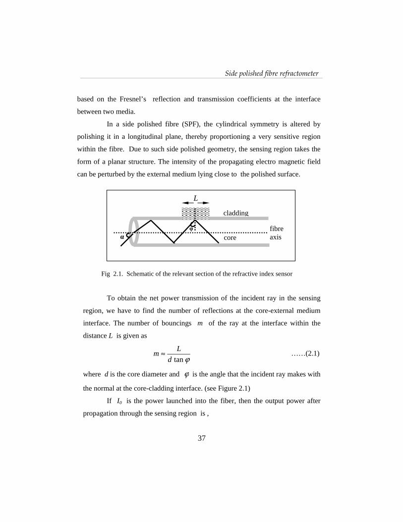
� ������������������������������������������������������������������ �� �� �������� �
37
based on the Fresnel’s reflection and transmission coefficients at the interface
between two media.
In a side polished fibre (SPF), the cylindrical symmetry is altered by
polishing it in a longitudinal plane, thereby proportioning a very sensitive region
within the fibre. Due to such side polished geometry, the sensing region takes the
form of a planar structure. The intensity of the propagating electro magnetic field
can be perturbed by the external medium lying close to the polished surface.
Fig 2.1. Schematic of the relevant section of the refractive index sensor
To obtain the net power transmission of the incident ray in the sensing
region, we have to find the number of reflections at the core-external medium
interface. The number of bouncings m of the ray at the interface within the
distance L is given as
ϕtand
Lm ≈ ……(2.1)
where d is the core diameter and ϕ is the angle that the incident ray makes with
the normal at the core-cladding interface. (see Figure 2.1)
If I0 is the power launched into the fiber, then the output power after
propagation through the sensing region is ,
L
�
� core fibre axis
cladding

����� ���
38
mRII 0≈ ……(2.2)
where 2
rR = and r is the Fresnel’s coefficient of reflection.
In our model, we do not consider any specific polarization state of the
incident light beam and ‘r’ is the coefficient of reflection for an arbitrary
polarization. From Fresnel’s reflection, the general behaviour of the sensor can
be explained as follows. Liquids having refractive indices much lower than that
of the core, yield the same maximum output power since all the rays undergo
total internal reflection. As the refractive index of the liquid approaches the core
refractive index, the output power decreases sharply. For refractive indices larger
than the core, the output intensity shows only slow increase. The problem with
this design is that the sensitivity is very poor for refractive indices which are
much smaller than the core refractive index[23,24] and this sets a limit to the
operating range of the sensor.
In order to improve the performance at the low refractive index region,
we studied the effect of the launching angle and fibre geometry. The theoretical
analysis on how these parameters could improve the sensor performance is
discussed in the following sections.
2.2.2. Performance of the sensor with launching angle as the varying
parameter
2.2.2.1 Case (i): Straight fibre
As inferred from equation (2.2), we see that the sensor response to the
refractive index of the cladding material depends on both reflectance at the core-
cladding interface and the number of reflections in the sensing region. These two
parameters depend on � - the angle which the ray incident at the core-cladding
interface makes with the normal, which in turn is determined by the launching
angle � (fig 2.1). Applying Snell’s law and Fresnel’s reflection coefficients in

� ������������������������������������������������������������������ �� �� �������� �
39
equation(2.2), we can simulate the dependence of sensor response on the
launching angle.
Figure 2.2 shows the power loss through the fibre for different cladding
refractive indices at different launching angles. The simulated results are for the
fibre parameters, ncore = 1.49, d =0.980 mm, and L = 2 cm .
Fig 2.2 Simulation of transmission characteristics in straight fibre for different launching angles α varying between 00 to 300
We observe that the sensing range of refractive index strongly depends
on the launching angle �. At smaller launching angles, the sensor has no
response in the low-refractive index region. As � increases, the sensitivity at
the low refractive index region increases, thereby increasing the sensing range.
From fig 2.2, we can infer that for a fibre with numerical aperture (NA) 0.5,

����� ���
40
maximum sensing range is obtained for �=300, which corresponds to the
acceptance angle of this fibre. Increasing the launching angle (�), further will
enhance the sensing range which implies that POFs with larger numerical
aperture can be employed for a wide dynamic range of refractive index
measurement. For large values of � , the corresponding angle � will be less
than the critical angle for the core-liquid interface, even for lower values of nliq .
This simply means that higher order modes (those corresponding to larger � ) fail
to satisfy the guiding condition , even for small values of nliq and leak to the
cladding liquid, while lower order modes will satisfy the guiding condition for all
values of nliq < ncore.
2.2.2.2 Case (ii): Bent fibre
In the case of a straight fiber, the incident angle (at the core-cladding
interface) of a guided ray launched into the fiber remains the same in the sensing
region. Thus for a given launching angle, the value of ϕ remains the same for
the whole probe region and hence gives fixed values for the number of
reflections at the core-cladding interface (m) and reflection coefficient (r) for a
particular value of the refractive index of the cladding. Therefore for a given
fibre with a specific launching angle, a decrease in the value of ϕ causes
increase in m and decrease in r, thereby increasing the transmission loss through
the sensor. In the case of a bent fibre, as the ray enters the bent region , the angle
that the ray makes with the normal to the core-cladding interface at the outer
surface of the bent region decreases [27] as seen in fig(2.3).

� ������������������������������������������������������������������ �� �� �������� �
41
Fig 2.3 Propagation of meridional ray along a curved fibre showing the relevant parameters
Considering only meridional rays, the angle 'ϕ for the bent region is
given by
( )ϕϕ sinsin 1' K−= ……(2.3)
with ( )( )dR
hRK
++= where d is the core diameter, R is the
bending radius, h is the distance at which the ray is incident on the entrance of
the bent section of the fibre from the core-cladding boundary ( dh ≤≤0 ) . [27]
When K=1, equation (2.3) reduces to that for a straight fibre. The
sensitivity of the device for a particular cladding refractive index depends on the
value of K and ϕ . A decrease in the value of K and ϕ increases the power
loss through the sensing region. The value of K can be lowered by decreasing the
bend radius R.
R
R+d
α ϕ'

����� ���
42
We have already seen in the case of straight fibres with NA=0.5 that the
sensing range is maximum for a launching angle of 300. Keeping � as 300 , the
transmission loss for bent fibres for different values of K can be simulated. ( fig
2.4 )
Fig 2.4 Simulation of transmission characterisitics for bent fibres with launching angle 300
As is clear from fig 2.4, by decreasing K, sensor response at lower
refractive index region gets improved. We see that with a suitable combination
of launching angle and bent radius, the operating range can be tuned as per our
requirements.

� ������������������������������������������������������������������ �� �� �������� �
43
2.3 Fabrication of sensor head
The optical fibre used in the experiment was a standard commercial step
index polymer optical fibre (POF) with a polymethylmethacrylate (PMMA) core
of diameter 0.980mm surrounded by a thin cladding layer of fluorinated polymer.
The core refractive index (ncore) was 1.49 and the numerical aperture was 0.5.
For side polishing, fibres are usually held in a host-block as protection which
allows polishing and prevents the fibre from breaking. The host materials
commonly used for this purpose are fused silica, etched silicon V-grooves and
epoxy resins [13,28,29]. A small length (about 10 cm) of the fibre was inserted
into a curved metallic frame bent to a radius of 2 cm and the whole piece was
encapsulated in a block of resin. From the top side, the sheath was removed from
a small length (2 cm) of the fibre and was polished until the core region was
exposed. Polishing was done using silicon carbide powder and alumina powder
of two different grades (0.3µ and 0.05µ) . A small cuvette was also attached to
the resin block (Fig 2.5)
Fig 2.5 Side Polished POF sensing element
Resin block Polymer fiber
cuvette
Uncladded polished region

����� ���
44
2.4 Experimental Results and Discussion
We have seen that bent fibres are more sensitive than straight ones, so
experiments were conducted with bent fibre sensor head. Freshly prepared
sucrose solutions with known refractive indices were poured into the cuvette so
as to cover the unclad portion. The height of the liquid level is an important
parameter which affects the power loss in the sensing region. When a very thin
layer of liquid is taken, the rays reflected at the liquid-air interface will go back
to the core. However, when the thickness of the liquid layer is increased to a
certain level, the reflected rays at the liquid-air interface no longer enter the core,
thereby causing greater power loss than in the case with thin cladding layer.
Beyond this level, the output power remains constant even with further increase
in the liquid layer thickness.
The device can be developed by either forming a very thin layer of liquid
cladding (by adding a few drops of liquid on the polished section) or by forming
a thick layer of liquid cladding over the polished section. When working with
very thin liquid layers, the level height should be accurately measured and should
be maintained for all sets of measurements, which make the device more
complicated. Therefore the latter method was used for the present studies. We
have carried out the experiments with liquid layer thickness of 1mm. The analyte
volume required for this arrangement was only less than 0.5 ml. The temperature
of the sample solutions were maintained at 200C.
As inferred from our theoretical model sensing range increases for
higher launching angles to the fibre. In order to tune the range of the sensor to
our requirements a selective excitation at higher launching angles was done. For
this, the laser source was mounted on a precision rotation stage so as to change

� ������������������������������������������������������������������ �� �� �������� �
45
the launching angle into the fibre. Schematic of the experimental setup is given in
fig (2.6).
Fig 2.6 Experimental setup for refractive index measurements L – He-Ne laser(632.8 nm), R- rotation stage, SPFS- side polished fibre sensor, D-detector (Newport -818-SL)
A parallel beam of light from a He-Ne laser (632.8 nm) was incident on the fibre
tip which is positioned to be always at the centre of the precision rotator so as to
facilitate accurate angle measurement. The light transmitted through the sensor
was coupled to a Si detector(New Port 818-SL) with a power meter (Newport
1815C). The transmission output of the sensor was normalized to that in air.
The sensor output for different launching angles is shown in fig(2.7).
There is fairly good agreement between the theory and experimentally obtained
results, especially in the tuning of the sensing range by varying launching angle.
laser
� Fibre axis
fibre
L SPFS D
R

����� ���
46
1.30 1.35 1.40 1.45 1.50
-1.0
-0.8
-0.6
-0.4
-0.2
0.0
0 degree 10 degree 20 degree 30 degree
rela
tive
outp
ut (d
B)
refractive index
Fig 2.7 Sensor response for various launching angles. Accuracy of data points are better than 0.4%
We can see that the operating range of the sensor increases with the
launching angle (see Table 2.1) which can be well explained on the basis of our
theoretical model described in the previous sections. For �=300, we get the
maximum sensing range 1.333 – 1.477 refractive index units(RIU) and maximum
sensitivity -6.219 dB/RIU.
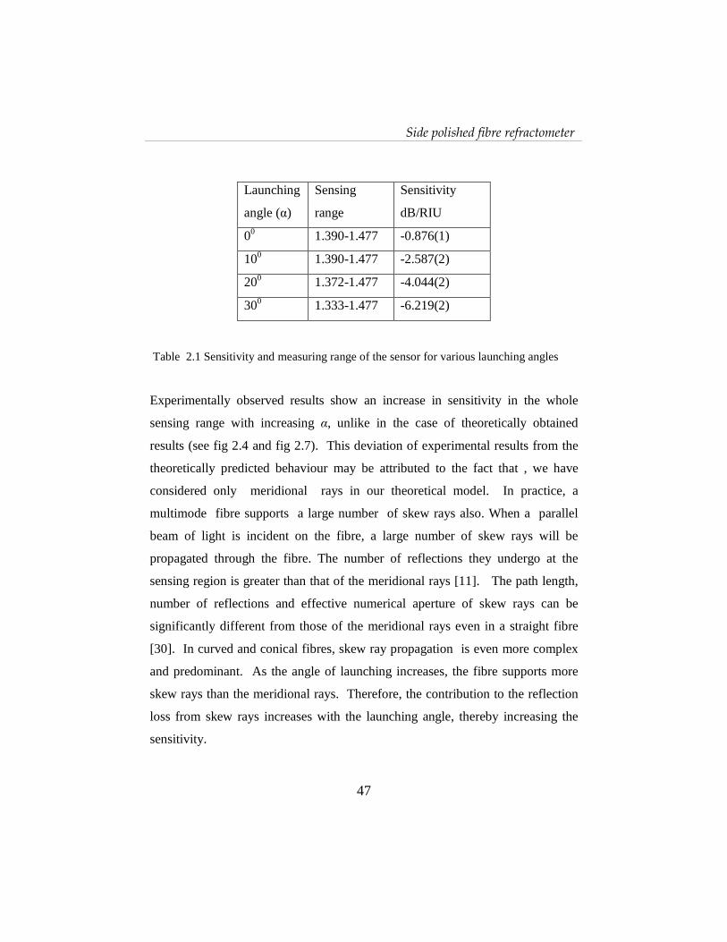
� ������������������������������������������������������������������ �� �� �������� �
47
Table 2.1 Sensitivity and measuring range of the sensor for various launching angles
Experimentally observed results show an increase in sensitivity in the whole
sensing range with increasing �, unlike in the case of theoretically obtained
results (see fig 2.4 and fig 2.7). This deviation of experimental results from the
theoretically predicted behaviour may be attributed to the fact that , we have
considered only meridional rays in our theoretical model. In practice, a
multimode fibre supports a large number of skew rays also. When a parallel
beam of light is incident on the fibre, a large number of skew rays will be
propagated through the fibre. The number of reflections they undergo at the
sensing region is greater than that of the meridional rays [11]. The path length,
number of reflections and effective numerical aperture of skew rays can be
significantly different from those of the meridional rays even in a straight fibre
[30]. In curved and conical fibres, skew ray propagation is even more complex
and predominant. As the angle of launching increases, the fibre supports more
skew rays than the meridional rays. Therefore, the contribution to the reflection
loss from skew rays increases with the launching angle, thereby increasing the
sensitivity.
Launching
angle (�)
Sensing
range
Sensitivity
dB/RIU
00 1.390-1.477 -0.876(1)
100 1.390-1.477 -2.587(2)
200 1.372-1.477 -4.044(2)
300 1.333-1.477 -6.219(2)

����� ���
48
The temporal response of the sensor for various analyte refractive
indices is given in fig 2.8.
0 5 10 15 20 25
0.540
0.545
0.550
0.555
0.560
0.565
0.570
0.575
0.580
(a)
Out
put P
ower
(A.U
)
Time (seconds)0 2 4 6 8 10 12 14 16 18
0.55
0.56
0.57
0.58
0.59
0.60
0.61
(b)
Out
put P
ower
(A.U
)
Time (seconds)
0 2 4 6 8 10 12 14 16 18 200.54
0.55
0.56
0.57
0.58
0.59
0.60
0.61
0.62
(c)
Out
put p
ower
(A
.U)
Time (seconds)
Fig 2.8 Temporal response of the sensor for cladding liquid refractive indices
(a) 1.333 (b) 1.420 (c) 1.465
The data acquisition was done by interfacing the detector with a PC using
Labview 7.0. The temporal response of the sensor was found to be less than 1
second, which is limited by the sampling rate of the detecting scheme. The
response time for the refractive indices within the operating range was found to
be almost the same.

� ������������������������������������������������������������������ �� �� �������� �
49
The proposed sensor can be made cost effective by using LED as the
light source. The low cost, simplicity, miniature size and compact nature make
the present refractometer more attractive for various industrial applications. The
sensitivity and sensing range can be tuned to our requirements by appropriately
adjusting the launching angle and curvature of the fibre. With this device, only
less than 0.5 ml sample is required for sensing and hence it is suitable for
measurements when the available quantity of the analyte is very small.
2.5 Conclusions
We have presented a refractive-index sensor exhibiting a wide dynamic
range using side polished polymer optical fibres. A novel method for tuning the
sensitivity and sensing range by selective excitation at higher launching angles in
a bent fibre has been discussed. For a slightly bent polymer optical fibre with
numerical aperture 0.5, maximum sensitivity and sensing range was obtained for
the excitation with a parallel beam of light, launched at an angle 300 with respect
to the fibre axis. The response time of the sensor was found to be less than 1
second. Since the quantity of sample required for the present sensing mechanism
is very less (about 0.5 ml), one can effectively employ this sensor for bio-sensing
applications and other cases where the amount of the samples available is very
small.
References
1. Hiroshi Yoshimura, J. Phys .E : Sci. Instrum, 21, 571-578 (1988). 2. G. H. Meeten, A. N. North , Meas. Sci. Technol, 2, 441-447 (1991). 3. G. H. Meeten, A.N. North, Meas. Sci. Technol 6, 214-221(1995) . 4. T. Takeo, H. Hattori, Jpn.J.Appl.Phys 21(10), 1509-1512 (1982).

����� ���
50
5. A. Kumar, T.V.B. Subrahmoniam, A.D. Sharma, K. Thyagarajan, B.P. Pal, I.C. Goyal, Electron. Letts 20, 534-35 (1984).
6. J. Villatoro, D. Monzon-Hernandez and D. Talavera, Electron.Lett 40(2), 106-07(2004).
7. Thomas Lee S, P. Sureshkumar, K. Geetha, P. Radhakrishnan, C.P.G. Vallabhan and V.P.N. Nampoori, Proceedings of SPIE- International Society for Optical Engineering, 4920 (2002).
8. Kerstin Schroeder, Wolfgang Ecke, Rudolf Mueller, Reinhardt Willsch and Andrey Andreev, Meas. Sci. Technol 12, 757-764(2001) .
9. C. Ronot-Trioli, A. Trouillet, C. Veillas, H. Gagnaire, Sensors and Actuators A 54, 589-593 (1996) .
10. Radan Slavik, Ji�í Homola, Ji�í �tyroký, Sensors and Actuators B 54 , 74-79 (1999).
11. A. Trouillet, C. Ronot-Trioli, C.Veillas and H. Gagnaire, Pure Appl.Opt 5, 227-237 (1996) .
12. M. Mitsushio, S. Higashi, M.Higo, Sensors and Actuators A 111, 252-259 (2004).
13. S. M.Tseng and C.L.Chen, Appl. Opt. 31(18), 3438-47(1992). 14. Ainhoa Gaston, Ibon Lozano, Fatima Perez, Fernando Auza, Joaquin Sevilla,
IEEE Sensors Journal 3(6), 806-810 (2003) 15. Kyung-Rak Sohn, Kwang-Taek Kim, Jae-Won Song, Sensors and Actuators A
101, 137-142 (2002). 16. S. Lee, J. Sokoloff, B. McGinnis, and H. Sasabe, Appl. Opt. 37, 453-462 (1998). 17. N. Chen, S. Chi, and S. Tseng, Opt. Lett. 29, 2219-2221 (2004). 18. R. Philip Chandy, P.J. Scully, P. Eldridge, H.J. Kadim, M. Gérard Grapin, M.G.
Jonca, M. Gérard D’Ambrosio and F. Colin, IEEE J. on Selected topics in Quantum Electronics, 6(5), 764-772 (2000) .
19. R. Philip Chandy, P.J. Scully and D. Thomas, Sensors and Actuators B 71, 19-23 (2000).
20. Shinzo Muto, Osamu Suzuki, Takashi Amano, Masayuki Morisawa, Meas. Sci. Technol. 14, 746-750(2003).
21. M. Morisawa, Y. Amemiya, H. Kohzn, C. Xin Liang and S. Muto, Meas. Sci. Technol 12, 877-881(2001) .
22. K.S.C. Kuang, W.J. Cantwell, P.J. Scully, Meas. Sci. Technol. 13, 1523-1534 (2002).
23. Joseba Zubia, G. Garitaonaindiá and Jon Arrúe, Appl. Optics 39(6), 941-946 (2000).
24. R.M. Ribeiro, João L.P. Canedo, Marcelo M. Werneck, Liliana R. Kawase, Sensors and Actuators A 101, 69-76(2002)
25. M. Sheeba, M. Rajesh, C.P.G. Vallabhan, V.P.N. Nampoori , P. Radhakrishnan, Meas. Sci. Technol 16, 2247-2250 (2005).
26. Yi-Zhen Lin, Jing-Hong Zhan, Shiao-Min Tseng, IEEE Photonics Tech. Lett. 9(9), 1241-1243 (1997)

� ������������������������������������������������������������������ �� �� �������� �
51
27. B. D. Gupta, H. Dodeja, A.K. Tomar, Opt. Quantum Electron 28, 1629-39, (1996) .
28. R. Alonso, F. Villuendas, J. Tomos and J.Pelayo, Sens and Actuators A 37-38, 87-192 (1993).
29. Javier Senosiain, Idoya Diaz, Ainhoa Gaston and Joaquin Sevilla, IEEE Trans on Instrumentation and Measurement 50(6), 1656-1660 (2001).
30. N.S. Kapany, Fibre Optics – Principles and Applications, Academic Press, NewYork (1967)

53
��������������������������������������������������� ��������������� ��������������� ��������������� ������������ ����� ����� ����� ������������������������� ����������������� ����������������� ����������������� �����
����
��� ���������� ���� ���� ����� ����� � �� � ��������� ������� ��� ����� ������ ��� ����������� �� ��� ����������������� � ��� ��������� ������� �� ������ ��������� �������������������� �� ������������ � ��� ��������� ��������������� ���� ����� ��� � �������� ���� ������ � �� ������� �� ������ ������������ ������������������������� ����������� ���������

����������������������������������������������������������������������������������������� ��
55
3.1 Introduction
During the past two decades, there has been a rapid growth in research
and development activities of fibre optic chemical sensors employing a number
of different strategies. The most popular among them are the absorption-based
and fluorescence based systems. In the absorption based system, the sensing fibre
uses the evanescent field extending from the core so as to interact with the
chemical species [1-5]. This technique is of particular interest for it allows the
development of distributed sensor systems. Fluorescence based systems also
rely on absorption, but the sensing is performed by monitoring changes in the
intensity or lifetime of the fluorescent light generated by the species or an
intermediate dye [6,7]. It should be noted that the waveguide design plays a
crucial role in optimizing the sensor performance.
One of the new techniques in the design of fibre optic sensors is the
usage of side polished fibres. Compact side polished fibre sensors are being
deployed in various industrial and medical markets. Sensors based on side
polished fibres for measuring various physical and chemical parameters such as
pressure, temperature, humidity, refractive index and pH have been reported in
the recent years[8-12]. Side polished fibres have also been used to develop
devices such as couplers, power monitors, filters and polarisers.[13,14].
Advantages of fibre optic sensors over commercially available
conventional sensors are many. However, from the applicability viewpoint, more
attention should be paid over certain key parameters such as cost, size and
sensitivity. In order to compete with the existing devices, novel fabrication
techniques, well suited for industrialization, have to be developed. The successful
design of such a device requires a thorough knowledge of the transmission loss
������ ���
56
characteristics through the sensor. Designing and optimizing the functions of
these devices can be made through numerical modeling as well as analytical
techniques.
This chapter deals with a theoretical study on the effect of a high
refractive index overlay on the sensitivity of an absorption sensor based on side
polished polymer optical fibre. Experimental verification was also performed, by
applying this sensor to study the reaction rate of a standard chemical reaction.
3.2 Complex refractive index and absorption
In order to model waveguide sensors, the absorption of a chemical
species at a given wavelength must be expressed in terms of a complex refractive
index. The relation between the quantities ∈ (molar extinction coefficient) or
mα (molar absorption coefficient) and the complex refractive index jkn − are
[15],
π
λαλ4
183.0C
Ck m=∈= .….. (3.1)
where C is the concentration of the chemical species and λ is the wavelength .
For a chemical species with large extinction coefficients or in high
concentrations, the real part of the refractive index ( n ) will also vary with the
solute concentration. In an optical waveguide or fibre sensor, changes in k
produce changes in the attenuation of the guided modes, that can be taken as a
measure of the sensitivity of the sensor. Small changes in the real part of the
index of the chemical species with concentration will affect the real part of the
propagation constant of the modes, but since this change is generally small

����������������������������������������������������������������������������������������� ��
57
compared to the real component itself, it has negligible effect on the attenuation
measurement.
3.3 Total internal reflection and Evanescent field
According to geometrical optics, as a light ray get total internally
reflected, the transmittance in the second medium is zero, implying that there is
no penetration of light in the second medium.
Fig 3.1 Light incident on an interface between two media – refraction and total internal reflection
In order to fully understand the phenomenon taking place at the dielectric
interface we should follow an electromagnetic treatment of the interface
problem[16].
For a uniform dielectric, the time independent wave equation is 2 2 2
0 0n k∇ + =E E .….. (3.2)
For TE incidence at angle 1θ , the above equation becomes
020
22
2
2
2
=+∂
∂+
∂∂
yyy Ekn
z
E
x
E ..….(3.3)
First considering the case of ordinary refraction, the field in each medium is
written as
1θ )(1 cθθ =
2θ
1θ
)90( 02 =θ
Medium 1 (n1)
Medium 2 (n2) z
x

������ ���
58
( )[ ] ( )[ ]1110111011 cossinexpcossinexp θθθθ xznjkExznjkEE Ry +−+−−= …..(3.4.a)
( )[ ]22202 cossinexp θθ xznjkEE Ty −−= …..(3.4.b)
Now consider the case when the input beam is incident at an angle greater than
critical angle. i.e., cθθ >1 . When total internal reflection occurs, a propagating
wave cannot arise in medium 2. The Snell’s law 2211 sinsin θθ nn = cannot
be satisfied or rather cannot be satisfied with a real value of 2θ . We can
satisfy it only with a complex value of 2θ such that
1sincos 12
2
2
12 −��
�
����
�±= θθ
nn
j ..….(3.5)
Using equation (3.5) in (3.4.b)
( )11012
2
2
1202 sinexp1sinexp θθ znjk
nn
xnkEE Ty −��
�
�
�−��
�
����
�±= …..(3.6)
Defining new parameters
20
22
2220
21110 ,,sin knknnk −=−== βγβκθβ ……(3.7)
We write,
( ) ( )zjxEE Ty βγ −−= expexp2 ……(3.8)
The solution no longer has the form of a plane wave propagating at an angle 2θ ,
because its x dependence is not a complex exponential. Instead it is a wave
whose amplitude distribution varies exponentially in the x-direction and that
propagates along the interface in the z-direction. This is called evanescent wave.

����������������������������������������������������������������������������������������� ��
59
A field of this type stores energy and transports it in the direction of propagation
(z) but does not transport energy in the transverse direction (Fig 3.2 ).
Fig 3.2 The exponentially decaying evanescent field in the cladding of the optical waveguide
The phase shift occurring on total internal reflection is given by κγ=Φtan for
TE incidence and κγ���
����
�=Φ 2
2
21tan
nn
for TM incidence.
This phase change is physically understood by the lateral shift of the
reflected beam from the trajectory predicted by simple ray theory analysis (Fig
3.3). This lateral displacement is called Goos-Haenchen shift.
Fig 3.3 The lateral displacement of a light beam on reflection at a dielectric interface (Goos-Haenchen shift)
Evanescent field
guide
cladding
n1>n2
n2
Standing wave
Lateral shift Penetration depth
Virtual reflecting plane
Reflecting interface
n2
n1>n2
1θ 1θ
������ ���
60
The geometric reflection appears to take place at a virtual reflecting
plane, which is parallel to the dielectric interface, in the lower index medium.
If the lower-index region contains an absorbing chemical species
( jknn −=2 ), then the reflection coefficient of the ray is less than unity owing
to evanescent wave absorption. In a waveguide/fiber, the evanescent wave
interacts with the chemical species surrounding the core region where the
cladding is being removed, giving rise to a phenomenon called Attenuated Total
Reflection (ATR). The amount of the absorption depends on both the amplitude of
the evanescent field in the low index medium and the number of reflections at the
interface. The former increases dramatically for incident angles approaching the
critical angle and the latter is inversely proportional to the waveguide thickness.
3.4 Ray optics approach to side polished fibre absorption sensor
The ray optics approach is the simplest way of calculating the
attenuation of a guided wave caused by an absorbing species in the cladding
region [15,17]. Consider a side polished fibre with core refractive index 1n and
cladding index 2n . In a side polished fibre (SPF), the cylindrical symmetry of
the fibre is altered via polishing in a longitudinal plane and the sensing region
takes the form of a planar structure. The intensity of the propagating electro
magnetic field can be perturbed by the external medium lying onto the polished
surface. Light transmission through the sensing region can be studied using ray
optics approach for a multimode planar waveguide.

����������������������������������������������������������������������������������������� ��
61
Fig 3.4 Side polished fibre with an absorbing liquid at the unclad portion
Let the lossy liquid be of a refractive index jkn −4 . If the ray trajectory
incident at an angle 1θ makes n reflections per unit length at the guiding layer -
lossy liquid boundary, then the attenuation of the guided wave due to the
chemical absorption is given by [15,17]
( )nr
PP 2
1
0 = ……(3.9)
where 0 1 and P P are the output and input powers and r is the reflection
coefficient of the ray at the guide-liquid interface.
The sensing region shown in fig 3.4 has got an asymmetric planar waveguide
structure. For such a structure, with the absorbing liquid on one side only, the
number of reflections per unit length is given by [15,17]
1tan2
1θed
n = ……(3.10)
where the parameter ed is the effective thickness corresponding to the mode.
''' dddd e ++= where 'd and ''d are evanescent field penetration depths in
the cladding and the absorbing liquid respectively.
The power loss in dB is then given by [15,17]
Loss = )(ln343.42
rn− ……..(3.11)
de d
n4-jk
n2
n1

������ ���
62
Fig 3.5 shows the attenuation curve at wavelength 632.8 nm for a side-polished
fibre surrounded by an absorbing liquid with 33.14 =n and 610161.2 −= xk .
The fibre has a core diameter 0.980 mm and refractive index 1.49. The curve is
plotted against the effective index 12 sinθβ n= .
Fig 3.5 Attenuation versus effective index for side polished fibre surrounded with an absorbing liquid with refractive index 1.33-j2.161x10-6
The highest sensitivity occurs for rays near cutoff ( 4n≈β ) where the
evanescent field is very large. A particular problem associated with achieving
significant evanescent field penetration in the sensing region is that the lead fibre
numerical aperture is considerably less than that in the core-liquid region.
Consequently it is impossible to launch bound rays which would be incident on
the core-liquid interface at angles close to the critical angle. By virtue of its
cylindrical geometry a fibre will sustain nonbound or tunneling modes which are
����������������������������������������������������������������������������������������� ��
63
launched into the fibre at angles greater than that the meridional numerical
aperture permits [18]. Higher order modes can be generated at the sensing region
by tapering the fiber at this location [19,20] or by bending [2,21]. A selective
excitation of higher order modes can also be done by changing the launching
angle to the fibre. Low order modes can be blocked using an annular beam mask
at launch [1].
3.5 Effect of a high index overlay on the sensitivity
One method to enhance the sensitivity of a side polished fiber sensor is
to give a high refractive index coating in the sensing region. This technique has
already been used in D-fibers for methane gas sensing [22]. It is necessary to
evaluate theoretically the attenuation properties of the waveguide sensor, for
optimizing the device for maximum sensitivity. The matrix method [23] is a
powerful tool for analyzing multilayer waveguides containing absorptive layers,
but the processes are rather complicated for the complex manipulations. Stewart
et al [22,24] evaluated the sensitivity enhancement of D-fiber sensors with high
index overlay using a 4 layer waveguide model, perturbation method and matrix
method . De-Kui Qing et al has done a group index method for the theoretical
evaluation of absorption coefficient of waveguide sensors, for various designs of
the sensing region [25].
The fibre chosen for our experimental work is a large core polymer fibre
with N.A = 0.5. The core diameter is 980 microns. Owing to the large diameter
of the fibre core, we followed a ray optics approach to our problem.
The sensing region can be considered as a planar leaky structure. In this
region, light is partially confined to the core by reflection mechanisms other than

������ ���
64
total internal reflection. The light transmission in the sensing region was
evaluated by the reflection in a 3-layered structure [26].
The reflection coefficient )(θir is given by [27]
)2exp(1)2exp(
)(033423
033423
dkirrdkirr
rii
iii
−+−+
=θ ..…. (3.12 )
Where θ - the angle the ray makes with the normal to the core-overlay interface
And si = for s-polarised light & pi = for p-polarised light.
Other terms are
23r - Fresnel’s reflection coefficients at the core-overlay interface
34r - Fresnel’s reflection coefficients at the overlay-liquid interface
0d - overlay thickness
d - core diameter
1θ - the angle of incidence at the core-overlay interface
2θ - the angle of incidence at the overlay-liquid interface
3k - transverse wave number in medium 3,
2303 cosθnkk = …… (3.13)
case (i) No overlay
Only the reflections at the core-liquid boundary need to be considered in this case
so that,
Fresnel’s reflection coefficient
( )[ ]( )[ ] 13
21
122
22
4
122
1
122
22
424
cossin
cossin
θθα
θθα
nnin
nninr
+−−
−−−= ..….. (3.14)

����������������������������������������������������������������������������������������� ��
65
Reflectance 2
24rR = ….. (3.15)
No. of reflections per unit length at the core-liquid boundary
1tan2
1θd
N = ..…. (3.16)
where d - core diameter
Loss in dB , 2
24ln343.4 rNL −= .…..(3.17)
case (ii) In presence of overlay
The reflection coefficient for the 3-layer structure should be applied.
)2exp(1)2exp(
033423
033423
dkirrdkirr
r−+−+
= ..…. (3.18)
2rRov = .….. (3.19)
No. of reflections per unit length at the overlay-liquid boundary
201
1 tantan1
θθ ddN
+= .…..(3.20)
Loss in dB , 2
1 ln343.4 rNLov −= …… (3.21)
We define the sensitivity Enhancement factor
L
LS ov= ……. (3.22)
For a given fibre, S depends on various parameters like,
(i) refractive index of the overlay ( 3n )
(ii) overlay thickness ( 0d )
(iii) angles 1θ and 2θ , which again depend on the launching angle to the fibre.

������ ���
66
3.6 Results and discussion
The sensor performance is simulated for various overlay refractive indices and
thicknesses. Figure 3.6 shows the attenuation for an overlay coated SPF for
different launching angles. The overlay refractive index 59.13 =n , core
refractive index 49.12 =n , and 670nmλ = . The loss experienced by the
modes depends on the effective mode index. We can roughly say that each mode
corresponds to a particular launching angle to the fibre. (Launching angle is the
angle between the fibre axis and the ray incident on the fibre end ).
Fig 3.6 Attenuation vs overlay thickness plot for a side polished fibre with overlay refractive index 1.59, for launching angles 50, 100, 200 and 300.

����������������������������������������������������������������������������������������� ��
67
We see that for higher order modes, corresponding to larger launching angles,
there is considerable loss even without overlay. When the overlay thickness is
increased, the loss is increased . There is an optimum overlay thickness for each
mode for which the loss is maximum. We also note that the factor by which the
loss gets enhanced with the overaly, is also different for different modes. Though
the maximum attenuation is attained with the highest order modes, the factor by
which the attenuation is increased is greater for lower order modes. Figures 3.7
(a) and 3.7(b) show the sensitivity enhancement factor vs overlay thickness plots,
for a given overlay index 1.59, and for various launching angles.
(a)
Fig 3.7 a Sensitivity enhancement vs overlay thickness plot for a side polished fibre with overlay index 1.59, for launching angles 40, 60 and 80.

������ ���
68
(b)
Fig 3.7 b Sensitivity enhancement vs overlay thickness plot for a side polished fibre with overlay index 1.59, for launching angles 150, 200, 250 and 300.
In a multimode fibre, the overall attenuation will be a weighted average over the
modal distribution. In general, a single mode fibre is better in terms of sensitivity
and stability since it can be designed for optimum sensing by employing its
fundamental mode.
Figure 3.8 shows the effect of overlay refractive index on the sensitivity of the
device. We see that by increasing the overlay refractive index, the sensitivity gets
improved .

����������������������������������������������������������������������������������������� ��
69
Fig 3.8 Overlay thickness vs sensitivity enhancement factor plots for different overlay refractive indices, at launching angle 100 The periodicity of the plots arise from the properties of thin film reflection [27].
We see that sensitivity enhancement could be achieved only by proper selection
of the thickness of the overlay.
3.7 Fibre optic sensor for chemical reaction kinetics
In the previous sections, we have discussed the effect of coating the unclad
fibre with a high refractive index overlay on the evanescent wave absorption. It
has been inferred from the theoretical modeling that the sensitivity gets increased

������ ���
70
when coated with a high index material. We now apply this to a sensor designed
for chemical reaction kinetics study.
Kinetic studies provide very valuable information about reaction
mechanisms. The conventional methods of studying rate coefficients are
volumetric analysis [28] and optical transmission [29]. A simple optical sensing
means for the determination of rates of time-dependent chemical reactions is
based on the principle of fibre optic evanescent wave absorption. There are not
many reported works on the study of chemical reaction kinetics using fibre optic
sensors except a few [30,31].
The reaction rate of a chemical reaction is a quantity that defines how the
concentration of a reactant or product changes with time. Consider a simple
time-dependent chemical reaction ,
R1 + R2 = P
Where R1 and R2 are the two reactants and P is the product evolved during the
reaction. The amount of P increases with time. If this product is an absorbing
one, then the evanescent absorption will definitely increase as the concentration
of P increases with time. As a result, the light at the output end of the fibre will
decrease with time. The rate of decrease of the output power will be directly
proportional to the rate of evolution of the product P. In other words, the
variation of output power is a measure of the reaction rate.
3.7.1 Working principle
For a step index multimode optical fibre whose cladding has been replaced by an
absorbing fluid sample, the power transmitted is written as,
0 exp( )P P Lγ= − ……(3.23)
where γ ηα= , in which η is the average evanescent ratio and α is
the bulk absorption coefficient, which is directly proportional to concentration of
����������������������������������������������������������������������������������������� ��
71
the absorbing species. For a time dependent chemical reaction, the concentration
of the absorbing fluid (ie., the concentration of the product of the chemical
reaction) increases with time. Therefore we can rewrite equation (3.23) as
( ) (0) exp( ( ) )P t P t Lγ= − ……(3.24)
and 10
2.303 (0)( ) log
( )P
tL P t
γ = ……(3.25)
The sensitivity of the sensor is generally determined by the rate of change of
transmitted power with concentration. The higher the value of γ , the greater
will be the sensitivity of the sensor. For a given length of the sensing region, the
sensitivity of the evanescent wave absorption primarily depends on the amplitude
of the evanescent field in the sensing medium and the number of reflections per
unit length within the sensing region. Higher values of these two factors will
essentially increase the sensitivity of the sensor.
3.7.2 Experiment and Discussions
The sensor head fabrication was done according to the procedure discussed in
Chapter 2. The length of the unclad region was 2.5 cm. To give high refractive
index coating over the polished core, Polystyrene with refractive index 1.59 was
chosen as the overlay material . Sensor heads with overlay thicknesses 1.2 µm
and 2 µm were prepared by dip coating.
An intensity stabilized diode laser giving peak emission at 670 nm was
used as the source. The output was coupled to a Si detector (New Port 818-SL)
which was interfaced with PC with Labview 7.0. Fig 3.9 shows the schematic
of the experimental set up.

������ ���
72
Fig 3.9 Experimental setup for time-dependent reaction kinetics study L – Diode Laser(670 nm), SPFS- side polished fibre sensor, D-detector (Newport -818-SL)
Experiments were conducted with bare fibre as well as with coated fibres.
A standard chemical reaction namely, the reaction between potassium
iodide (KI) and potassium peroxdisulphate (K2S2O8) was chosen for study.
Equimolar solutions (7mM) of both these reagents were prepared in distilled
water. The reaction resulted in the evolution of iodine according to the equation,
2 2 8 2 2 42 2KI K S O I K SO+ → +
During the reaction, iodine was produced in the reaction cell. The amount of
iodine liberated increases with time. Two drops of starch was added as indicator
so as to enhance the absorption.
Figure 3.10 represents the variation of absorption coefficient plotted
against time, corresponding to uncoated fibre, and coated fibres.
L SPFS

����������������������������������������������������������������������������������������� ��
73
Fig 3.10 Variation of absorption coefficient with respect to time for (a) bare fibre (b) fibre with coating thickness 1.2 µm (c) fibre with coating thickness 2 µm
The absorption coefficients of the three sensor heads show different values and
hence different sensitivities. Of the three, the uncoated fibre has got the smallest
absorption coefficient. The sensor with a coating thickness 1.2 µm has got
greater absorption coefficient than that of thickness 2 µm. We have already seen
0 500 1000 1500 2000 2500
0.00
0.01
0.02
0.03
0.04
(a)
Abs
orpt
ion
Coe
ffici
ent (
cm-1)
Time (sec)
0 500 1000 1500 2000
0.00
0.02
0.04
0.06
0.08
0.10
0.12
(c)
Abs
orpt
ion
Coe
ffici
ent (
cm-1)
Time (sec)
-500 0 500 1000 1500 2000 2500 3000 3500-0.05
0.00
0.05
0.10
0.15
0.20
0.25
0.30
0.35
0.40
(b)
Abs
orpt
ion
coef
ficie
nt (c
m-1)
Time (sec)

������ ���
74
that the evanescent wave absorption varies in a periodic fashion with overlay
thickness.
There is a trend to show a linear variation of absorption with time during
the initial phase. The time variation of the absorption coefficient is nonlinear
with a tendency of saturation at longer duration. The initial slope of the graph
was taken as the rate constant of the chemical reaction. The initial slopes
obtained for the three cases are the following :
Bare fibre : 0.28 x 10⁻⁴ sec-1
Coating thickness - 1.2 µm : 1.56 x 10⁻⁴ sec-1
Coating thickness - 2 µm : 0.96 x 10⁻⁴ sec-1
There is no given value in literature for the comparison of rate constant, which is
essentially a function of reactant concentration. So in order to check the
validity of the results obtained from the fibre measurements, we have to rely on
the spectroscopic measurements.
The same reaction was studied using a spectrophotometer (JASCO
UV/VIS/NIR V-570), operating in time scan mode, with wavelength fixed at 670
nm. The value of the rate constant obtained by this method was 1.87 x 10⁻⁴ sec-1
which is close to that obtained using a fibre sensor head with overlay thickness
1.2 µm. The other two designs, fail to give correct values, most probably due
to low sensitivity. The effect of the overlay coating is to enhance the sensitivity
of the fibre sensor.

����������������������������������������������������������������������������������������� ��
75
3.8 Conclusions
In this chapter we have discussed the effect of high refractive index overlay on
the evanescent wave absorption . The effect of overlay thickness and refractive
index on the sensitivity of the sensor has been numerically modeled. Details of
the modeling related to the evanescent wave absorption for different overlay
refractive indices and overlay thicknesses are also included in this chapter. It
was observed that the evanescent wave absorption coefficient increased with
increase in overlay refractive index and proper selection of overlay thickness.
Experiments were also performed for studying the reaction kinetics of a standard
chemical reaction. A side-polished polymer fibre sensor coated with a higher
refractive index material was developed to study chemical reaction kinetics. The
coated fibre showed enhancement in sensitivity as compared to bare fibre.
References 1. V. Ruddy, B. D. MacCraith, J.A. Murphy, J. Appl. Physics 67 (10), 6070-6074
(1990). 2. I. Schnitzer, A. Katzir, U. Schiessi, W. J. Riedel, M. Tacker, J. Appl. Physics 66 (11), 5667-5670 (1989). 3. Culshaw 4. S. Thomas Lee, P. Suresh Kumar, K. P. Unnikrishnan, V. P. N. Nampoori, C. P.
G. Vallabhan, S. Sugunan, P. Radhakrishnan, Meas. Sci. and Technol. 14, 858-861 (2003).
5. P. Suresh Kumar, S. Thomas Lee, C P G Vallabhan, V.P.N. Nampoori, P. Radhakrishnan, Optics Commun. 214(1-6), 25-30 (2002).
6. Wolfgang Trettnak, Marc. J.P. Leiner, Otto S. Wolfbeis, Analyst 113, 1519-1523(1988).
7. E. Toba, J. Kazama, H. Tanaka, T. Nishimatsu, H. Aizawa, H. Ishizawa, IEICE Trans. Electron. E83-C, 366-370 (2000).
8. Ainhoa Gaston, Ibon Lozano, Fatima Perez, Fernando Auza and Joaquin Sevilla, IEEE Sensors Journal 3(6), 806-811 (2003)
9. Javier Senosiain, Idoya Diaz, Ainhoa Gaston and Joaquin Sevilla, IEEE Trans. On Instrumentation and Measurement 50(6), 1656-1660(2001).

������ ���
76
10. Joseba Zubia, German Garitaonaindia and Jon Arrue, Appl. Optics 39(6), 941- 946 (2000). 11. R.M. Ribeiro, João L.P. Canedo, Marcelo M. Werneck, Liliana R. Kawase, Sensors and Actuators A 101, 69-76(2002) 12. Navneet K. Sharma, B.D. Gupta, Optics Commun. 216, 299-303 (2003). 13. S. M. Tseng and C.L. Chen, Appl. Opt. 31(18), 3438-47(1992). 14. N. Chen, S. Chi, and S. Tseng, Opt. Lett. 29, 2219-2221 (2004). 15. G. Stewart, J. Norris, D. F. Clark, B. Culshaw, Int. J. Optoelectron. 6(3), 227-
238 (1991). 16. Richard Syms, John Cozens, Optical Guided Waves and Devices, McGraw-Hill
Book Company Europe, England (1992) 17. G. Stewart, B. Culshaw, Opt. And Quantum Electron. 26, S249-S259 (1994). 18. N.S. Kapany, Fibre Optics – Principles and Applications, Academic Press,
NewYork (1967) 19. P.M. Shankar, L.C. Bobb, H.D. Krumboltz, J. Light. Technol. 9(7), 832-
837(1991). 20. F. J. Arregui, I.R. Matias, M. L. Amo, Sens. Actuat A 79, 90-96 (2000). 21. S. K. Khijwania, B.D. Gupta, Opt. Quantum Electron. 31, 625-636 (1999). 22. F.A. Muhammad, G. Stewart, W. Jin, IEE Proceedings-J 140(2), 115-
118(1993). 23. A.K. Ghatak, K. Thyagarajan, M.R. Shenoy, J. Light. Technol. 5(5), 660-
667(1987). 24. F.A. Muhammad, G. Stewart, Electron. Lett. 28(13), 1205-1206(1992). 25. De-Kui Qing, Xiao-Min Chen, Kiminori Itoh, Masayuki Murabayashi, J. Light.
Technol. 14(8), 1907-1917(1996). 26. Yi-Zhen Lin, Jing-Hong Zhan, Shiao-Min Tseng, IEEE Photonics Tech. Lett.
9(9), 1241-1243 (1997) 27. Max Born and Emil Wolf, Principles of Optics 7th Edn , Cambridge University
Press (1999). 28. D.P. Shoemaker and C.W. Garland, Experiments in Physical Chemistry,
McGraw-Hill, Tokyo (1967). 29. W.D. Prudy, F. Tarczynski, Proc. SPIE 3537, 26-33 (1998). 30. P. Radhakrishnan, V.P.N. Nampoori, C.P.G. Vallabhan, Opt. Engg. 32(4), 692-
694 (1993). 31. P.K. Choudhury, Toshihiko Yoshino, Meas. Sci. Technol. 13, 1793-1797(2002).
77
���������������������������������������������������������������������������������������� ��������� ��������� ��������� ���������������������������������������������������������������������������������������������������������������������������������������������
�
������������������ ����������������������������� ��������������������������������������������������������������������������������������������������������������������������� ���� �� ��������� ���� ��������� ������ �������������������������������������������������������� ��������������� ���� ����� ��� �� ��� �������� �� �����������������������������������!����
4

� ����������������������������������������������������������������� �����������
79
4.1 Introduction
Organic dye lasers have become a subject of intensive research ever
since Sorokin and Lankard reported the stimulated emission from an organic dye
solution [1]. The use of solid matrix for dye lasers gets rid of many of the
common problems associated with liquid systems like concentration variation
due to evaporation of solvents. Solid state dye lasers offer added technical
advantages such as compactness, manageability and versatility. The first attempt
to develop solid-state dye lasers were reported in the late 1960’s [2,3]. Ever
since there have been intensive efforts to achieve the incorporation of organic
dyes in solid matrices that might replace conventional liquid dye lasers. Most of
the recent works have been done using either polymers [4,5] or silica gels [6,7] as
the host media. Polymeric materials in particular offer advantages such as ease
of processing, which permits fabrication of devices of virtually any shape and
potentially cost-effective. Organic polymers poly methyl methacrylate (PMMA)
and co-polymers of MMA such as HEMA [8-11] have been widely used as host
material for laser dyes. Other commonly used polymer hosts include poly acrylic
acid (PA) [12] and poly vinyl alcohol (PVA) [13].
In the field of photonics, considerable attention is centering on the use of
polymer waveguides and fibers as they have a great potential to create all-optical
devices [14,15] and polymer optical integrated circuits. Polymers show better
optical transparency, homogeneity of refractive index and good compatibility
with organic dyes. Moreover, waveguide structure with its long interaction
length of active material is attractive as it is effective for controlling optical
signals with low input power. Polymer waveguides and fibres doped with
organic dyes have proved to be potential candidates for fibre lasers and

���������
80
amplifiers [16-19]. By choosing appropriate dyes, we can obtain laser emission
from doped polymer waveguide in the entire visible region. The combination of
signal processing in optically active organic materials along with a passive mode
of signal transmission in transparent polymers has been used in the design of
all-optical switches as well [20].
This chapter deals with the fabrication of dye doped polymer film
waveguides as well as their characterization. The properties of dye-doped
polymer waveguides should be clearly known before they are used for all-optical
devices. Improvement in the performance of these devices requires a thorough
knowledge of the optical absorption and emission characteristics. The loss
characterization was done by a non-destructive side-illumination fluorescence
[21,22] technique.
4.2 Materials
4.2.1 Host Material : Poly (methyl methacrylate) (PMMA)
Although, through the years, a number of different materials have been
tested as solid hosts for laser dyes, polymeric matrices present some important
advantages as they usually show good compatibility with organic dyes, have
excellent optical homogeneity [8] and are amenable to inexpensive fabrication
techniques which could facilitate both miniaturization and the design of
integrated optical systems. The basic requirements imposed on a polymeric host
for laser dyes are good optical transparency at both pump and lasing
wavelengths, good solubility of the dye in the material and resistance to pump
laser radiation against photochemical reaction and optical damages.

� ����������������������������������������������������������������� �����������
81
Due to its favourable properties we chose poly methyl methacrylate
(PMMA) for the present studies. The molecular structure of PMMA is shown in
fig 4.1. This polymer has been the most frequently used host for lasing dyes due
to its excellent transparency (with refractive index ~ 1.49 ) in the visible region
and its relatively high laser-damage threshold.
Fig 4.1 : Molecular structure of PMMA
4.2.2 Dye : Rhodamine 6G
Most of the dye lasers operate with the materials belonging to the
xanthene family of dyes, which cover the wavelength region from 500-700nm
and have generally very high quantum efficiency. The organic dye chosen for
the present studies is the chloride of rhodamine 6G (Exciton), which belongs to
the xanthene family of dyes. Fig 4.2 shows the molecular structure of the dye
molecule. Rhodamine 6G has been frequently investigated in solid state dye
lasers in a variety of solid hosts [8,10,23-26] on account of its high fluorescence
n CO2CH3
CH3
CH2 C

���������
82
quantum yield, low intersystem crossing rate and low excited state absorption at
both pump and lasing wavelengths.
Fig 4.2 Structure of Rhodamine 6G
The absorption maximum of rhodamines is surprisingly dependent on the
solvent, in particular with those dyes whose amino groups are not fully alkylated
( eg. Rhodamine 110 and rhodamine 6G). The fluorescence spectra of these
dyes closely resemble the mirror image of the long wavelength absorption band.
4. 3 Film Fabrication
Free standing films of Rhodamine 6G doped PMMA films were
prepared through tape casting method. Weighed PMMA (HIMEDIA, MWAv-
15000) granules were added to the pre-measured solvent- Methyl Ethyl Ketone
O H
H5C2
N C2H5
H
N
CH3
OC2H5
O
C
H3C
� ����������������������������������������������������������������� �����������
83
(MEK) (MERCK) in polypropylene jars (Tarson). Roll milling ensured complete
dissolution of PMMA. Rhodamine 6G was then added to this prepared PMMA-
MEK binder in desired concentration. Homogeneous mixing of the Rh6G in the
matrix was ensured by roll milling.
The mix prepared as above was cast into thin sheets on a glass plate
using double doctor blade tape casting technique (EPH Engineering, USA). This
technique is useful for obtaining films of uniform thickness. The mix was poured
through the gap between the blade and the glass plate. Desired thickness was
maintained by controlling the blade to glass bed gap and the casting speed. After
casting, the solvent evaporated leaving behind uniformly doped PMMA sheets.
The cast tapes were removed from the glass bed to get uniform films of
Rhodamine 6G doped PMMA. Films of various thicknesses and dye
concentrations were prepared using this technique. The films were then cut into
the size of 4cm x 2cm.
4.4 Absorption and emission spectra of the samples
The absorption spectra of the films were taken using a
spectrophotometer (JASCO UV/VIS/NIR V-570). (see fig 4.3).
The absorption spectra showed the peak at 536 nm with a shoulder near
500nm. Spectral characteristics did not show any dependence on dye
concentration except for the peak intensity which ensured the absence of any
aggregation of dye molecules.

���������
84
400 450 500 550 600 650 700
0.0
0.1
0.2
0.3
0.4
0.5
0.6
0.7
0.8 d
c
b
a
Abs
orba
nce
Wavelength (nm) Fig 4.3. Absorption spectra of rhodamine 6G doped thin films (50 µm thick) for dye concentrations (a) 0.1mM (b) 0.5mM (c) 1mM (d) 1.5mM
Fluorescence emission from the dye doped polymer film waveguides
were excited by the 532 nm (cw) from a diode pumped solid state (DPSS) laser
(Nd:YVO4). The front surface emission was focused to fall on the slit of a 0.2m
grating-monochromator (Mc Pherson). The output from the monochromator-
PMT assembly was given as input to a lock-in amplifier (SR-830) which was
interfaced with PC using Labview 7.0.

� ����������������������������������������������������������������� �����������
85
(a) (b)
Fig 4.4. (a) Front surface fluorescence emission from Rh6G doped 50 µm thick PMMA films for dye concentrations (1) 0.1mM (2) 0.5mM (3) 1mM (4) 1.5mM. Sharp peak at low wavelength side is due to the pump radiation. (b) Variation of peak fluorescence wavelength with dye concentration
From figure 4.4, we observe that the peak of the fluorescence spectrum from the
films gets shifted to longer wavelengths when the dye concentration is increased.
This concentration dependent red shift was observed for dye solutions as well
[27]. The red shift in peak fluorescence wavelength is a consequence of
secondary absorption effects due to the overlap between the emission spectrum
of the dye and the low energy tail of its absorption band [27].
A list of the environmental factors that affect fluorescence phenomena
includes interaction with solvents and other dissolved compounds, temperature,
pH and the concentration of the fluorescent species. Both the absorption and
emission spectra as well as the quantum yields of the fluorescent molecules are
520 540 560 580 600 620 640
0.000
0.001
0.002
0.003
0.004
0.005
0.006
0.007
43
2
1
Fluo
resc
ence
inte
nsity
(A
.U)
Wavelength (nm)0.0 0.5 1.0 1.5
550
552
554
556
558
560
Pea
k flu
ores
cenc
e w
avel
engt
h (n
m)
Dye concentration (in mM)
���������
86
influenced by these parameters. The absorption spectra did not show any
modifications with respect to dye concentration. This means that aggregate
formation at high concentrations had a negligible effect on the observed
fluorescence peak shift [ 28]. Hence the observed peak shift in the fluorescence
spectra is a consequence of self absorption and reemission [29]. Since the
emitted wavelength was longer than the absorbed one, self absorption of
fluorescence radiation results in the fluorescence emission at longer wavelength.
If the molecules have closely lying levels of different absorption cross section,
absorption saturation to each level would also lead to a wavelength shift.
However the red shift in the dyes is commonly attributed to the concentration
effects resulting in self-absorption.
4.5 Loss characterization
As noted earlier, the properties of dye-doped polymer waveguides should
be clearly known before they are used for all-optical devices. In order to optimize
the performance of these devices, a thorough knowledge of the optical
characteristics is essential. Optical attenuation in waveguides is one of such
important parameter. There are different techniques for measuring the
propagation losses in waveguide structures. Usually the propagation losses in
fibres and planar waveguide structures are measured by the cut-back
technique[30,31] which consists in comparing the transmittance of several
guides with different lengths at a specific wavelength. The values of the loss
parameter can also be extrapolated from a bulk measurement. The disadvantage
of the cut-back technique is that it is a destructive method. Bulk measurements
involve a broad band light source incident on a fixed length of the material and a
� ����������������������������������������������������������������� �����������
87
spectrometer to read the transmitted intensity. A non-destructive side-
illumination fluorescence technique (SIF) is an alternative to the above
mentioned techniques, for measuring the optical attenuation in dye-doped fibres
as well as waveguides [22,32,33]. This measurement technique requires a
monochromatic light source to illuminate the waveguide from the side. The
fluorescence collected from one end of the waveguide is used as a light source to
characterize the attenuation mechanisms in the planar waveguide structures. The
excitation spot is shifted so as to collect fluorescence that propagated through
various distances through the waveguide. Since the shorter wavelength light is
more strongly absorbed, the SIF technique is ideal for measuring the attenuation
coefficients at wavelengths in the tail of the absorption band of a dye molecule.
This property is extremely useful because standard methods fail to take accurate
measurements of attenuation coefficients in the tail region owing to the large
absorption at resonance. (See the absorption spectrum in fig 4.3)
4.5.1 Experimental set up
The schematic diagram of the experimental set up is shown in figure 4.5.
The film waveguide was mounted normally on a translation stage with respect to
the incident radiation. The excitation source was 532 nm (cw) from a diode
pumped Nd:YVO4 laser. The side illumination of the dye doped waveguide
generated fluorescence emission. The light emission from one end of the
waveguide was collected by an optical fibre leading to a monochromator-
photomultiplier tube assembly coupled with a lock-in amplifier (Stanford
Research Systems SR830), which was interfaced to a PC by Labview 7.0.

���������
88
Fig 4.5 Experimental set up to record the fluorescence emitted from side-illuminated planar waveguide C – Chopper L – Focusing lens W – Waveguide OF – optical fibre LA – Lock-in-Amplifier MPA – Monochromator PMT assembly. Arrow shows the direction of translation of the waveguide.
To measure the transmitted fluorescence as a function of propagation
distance through the waveguide, the illumination point on the waveguide was
varied by translating the waveguide horizontally across the laser source. The
direction of translation is indicated by an arrow mark in figure 4.5. The distance
between the point of illumination and the waveguide edge from which light is
collected is measured as ‘z’. At each point of illumination, the fluorescence
spectrum was charted. This was done for film waveguides with various dye
concentrations and thicknesses.
4.5.2 Results and discussion
Experiments were conducted on film waveguides with varying dye
concentrations (0.1mM, 0.5mM, 1mM and 1.5 mM ). The side illumination
fluorescence spectra were recorded for various propagation distances from one
edge of the waveguide, for pump power 3mW. Figure 4.6.a shows the spectra of
transmitted fluorescence light measured as a function of the propagation distance
L
OF
W
DPSS LASER
MPA
LA
C

� ����������������������������������������������������������������� �����������
89
(z) through the waveguide of thickness 50 microns and dye concentration 0.5
mM, for a pump power 3mW at 532 nm.
520 540 560 580 600 620 640 660 680-0.02
0.00
0.02
0.04
0.06
0.08
0.10
0.12
0.14
0.16
0.18
f
ed
c
b
a
Fluo
resc
ence
Inte
nsity
(A.U
)
Wavelength (nm) (a)
(b)
Fig 4.6. (a) Transmitted fluorescence as a function of propagation distance through the waveguide (a)z=3mm (b) z=6mm (c) z=9mm (d) z=12mm (e) z=18mm (f) z=24mm (b) Variation of fluorescence peak with propagation distance (film thick ness = 50 µm)
0 5 10 15 20 25 30 35
565
570
575
580
585
590
595
600
605
1.5 mM 1.0 mM 0.5 mM 0.1 mM
Pea
k flu
ores
cenc
e w
avel
engt
h (n
m)
z (mm)

���������
90
As the propagation distance increases, the magnitude of the output
intensity decreases due to various loss mechanisms such as absorption and
scattering. In addition, there is a red-shift for the peak fluorescence emission as
the illumination distance from one edge of the waveguide is increased. Similar
redshift in the fluorescence emission from side-illuminated dye doped fibre has
also been observed by other workers [32,33].
As indicated earlier, the redshift of the fluorescence signal is produced
by the self-absorption of the dye due to the overlapping of the absorption and
fluorescence spectra of Rh6G [27]. In the previous section we discussed the
concentration dependent red shift of the fluorescence. We observe a similar
behaviour on changing the distance of propagation through the waveguide. As
the fluorescence light is guided through the dye doped waveguide, the effective
pathlength is increased resulting in self-absorption and re-emission causing a
redshift in the observed spectrum. Farther the point of illumination from the
observation end, larger will be the effective path length which results in
enhanced interaction between the dye molecules and the fluorescence emission
generated. This results in an increased self absorption of the fluorescence and
thereby shifting the emitted fluorescence peak towards the red side.
Figure 4.6.b shows the variation of fluorescence peak wavelength as a
function of propagation distance through the waveguide. For shorter
propagation distances in the waveguide, the redshift shows a linear behaviour
whereas at longer distances, the shift tends to exhibit a saturation behaviour .
This type of nonlinear behaviour of fluorescence peak with respect to z is
predominant at higher dye concentrations as is clear from fig 4.6.b. This
mechanism is similar to the concentration dependent redshift which is observed
in dye solutions [27].

� ����������������������������������������������������������������� �����������
91
The fluorescence emission collected from the dye doped waveguide has
got a spectral width of about 100nm and hence can be used as a broad
wavelength light source for measuring the attenuation in the waveguide. The
transmitted fluorescence was measured as a function of the propagation distance
so as to characterize the attenuation in the waveguide.
From Beer-Lambert’s law for linear optical attenuation in a medium,
0( , ) ( ) exp( ( ) )I z I zλ λ α λ= − … (4.1)
where I(λ,z) and I0(λ) represent the intensity of the transmitted light at
wavelength λ at propagation distances z and z=0 respectively while α(λ) is the
linear attenuation coefficient corresponding to wavelength λ .
We first applied the Beer-Lambert law in our data so as to characterize
the optical loss in the waveguide. Figure 4.7 and 4.8 show plots of natural
logarithm of transmitted fluorescence intensity versus propagation distance
corresponding to various emission wavelengths, for film thickness 50 microns
and 135 microns respectively.

���������
92
Fig 4.7 ln(I) vs z plots for film thickness 50 µm and dye concentrations (a) 0.1 mM (b) 0.5 mM
0 5 10 15 20 25
-6
-5
-4
-3
-2
(a)
λ = 570 nm λ = 580 nm λ = 590 nm λ = 600 nm λ = 610 nm λ = 620 nm
ln(I
)
z (mm)
0 5 10 15 20 25-7
-6
-5
-4
-3
-2
(b)
λ=580 nm λ=590 nm λ=600 nm λ=610 nm λ=620 nm λ=630 nm
ln(I
)
z (mm)

� ����������������������������������������������������������������� �����������
93
Fig 4.7 ln(I) vs z plots for film thickness 50 µm and dye concentrations (c) 1 mM (d) 1.5mM
0 5 10 15 20 25 30
-8
-7
-6
-5
-4
-3
-2
-1
(c)
λ = 580 nm λ = 590 nm λ = 600 nm λ = 610 nm λ = 620 nm λ = 630 nm λ = 640 nm
ln(I)
z(mm)
0 5 10 15 20 25-10
-9
-8
-7
-6
-5
-4
-3
-2
-1
(d)
λ = 580 nm λ = 590 nm λ = 600 nm λ = 610 nm λ = 620 nm λ = 630 nm λ = 640 nm
ln (I
)
z (mm)

���������
94
Fig 4.8 ln(I) vs z plots for film thickness 135 µm and dye concentrations (a) 0.1 mM (b) 0.5mM
0 5 10 15 20 25
-6
-5
-4
-3
-2
(a)
λ=570 nm λ=580 nm λ=590 nm λ=600 nm λ=610 nm λ=620 nm
ln(I)
z (mm)
0 5 10 15 20 25-6
-5
-4
-3
-2
-1
(b)
λ=580 nm λ=590 nm λ=600 nm λ=610 nm λ=620 nm λ=630 nm
ln(I)
z (mm)

� ����������������������������������������������������������������� �����������
95
Fig 4.8 Ln(I) vs z plots for film thickness 135 µm and dye concentrations (c) 1 mM (d) 1.5m M
0 5 10 15 20 25
-8
-7
-6
-5
-4
-3
-2
-1
(c)
λ=580 nm λ=590 nm λ=600 nm λ=610 nm λ=620 nm λ=630 nm
ln(I
)
z (mm)
0 5 10 15 20 25
-9
-8
-7
-6
-5
-4
-3
-2
-1
(d)
λ=580 nm λ=590 nm λ=600 nm λ=610 nm λ=620 nm λ=630 nm λ=640 nm
ln(I)
z(mm)

���������
96
For samples with thickness 50µm and a low dye concentration (0.1 mM), the
ln(I) vs z plots are linear. The observed linearity suggests that the attenuation
mechanisms in the waveguide is linear and hence could be explained by the
Beer-Lambert’s law. For dye concentrations above 0.1 mM it is observed that
the nonlinear behaviour of the ln(I) vs z plots is pronounced. The plots cannot
be fitted to a single straight line. Each plot can be peeled off to different straight
lines with different slopes.
0 5 10 15 20 25-4.5
-4.0
-3.5
-3.0
-2.5
-2.0
αααα= 0.077+0.01
αααα= 0.165+0.01
αααα= 0.103 +0.01
ln(I)
z (mm)
Fig 4.9 ‘Peeling of curve’ method applied to ln(I) vs z plot at �=600 nm. Figure clearly indicates different values of α at three regions of propagation distance.

� ����������������������������������������������������������������� �����������
97
Figure 4.9 shows the ln(I) vs z plot peeled into 3 straight lines , for waveguide
with dye concentration 1 mM and thickness 50 microns giving attenuation
coefficients of 0.165 mm-1, 0.103 mm-1 and 0.077 mm-1 respectively at short,
medium and long propagation distances..
At a higher thickness (135 µm), the sample with dye concentration 0.1
mM also exhibits this nonlinear behaviour. This means that for the same dye
concentration, with an increased film thickness, a behaviour similar to that
observed in films with higher dye concentration is observed. This can be justified
as follows. By increasing the film thickness, the number of interacting dye
molecules gets increased, and in effect is similar to the case of increasing dye
concentration. For higher dye concentrations, irrespective of film thickness, the
plots show non linearity which indicates more complex attenuation mechanisms.
In other words, the nature of the attenuation coefficient � in these samples is
determined by various parameters such as dye concentration, waveguide
thickness and length of propagation through the waveguide. The exact nature of
� cannot be fully known from our observations
The optical attenuation in dye doped PMMA waveguides can be due to
several factors such as absorption by the dye, absorption by the host material and
scattering. Out of these, the main factor contributing to the attenuation is the
absorption due to dye molecules. The attenuation of PMMA in the visible
wavelength region is very low [34,35] and hence we do not consider the
contribution from the host material to the optical attenuation. For rhodamine
dyes, the absorption and emission bands overlap, and hence a part of the emitted
light is reabsorbed, which gets reemitted at a longer wavelength. As the
fluorescence propagates through the sample, the intensity of the peak emission
decreases with increasing length. In addition, a red shift in the peak wavelength

���������
98
is also observed, due to self absorption and reemission as described above.
While studying the attenuation mechanisms inside a dye doped waveguide, all
these effects should be considered. In such a case, the attenuation coefficient for
a particular wavelength ( )λα does not remain the same throughout the entire
length of propagation – as inferred from our observations – but will be a
function of propagation distance z so that ,
( )zαα = …… (4.2)
We distinguish the following two cases for optical attenuation coefficient
in the waveguide.
Case (i) Only absorption of the pump beam is present inside the waveguide
Light at wavelength λ with initial intensity 0I , will decrease in its intensity with
the propagation distance z . Let I be the intensity at any length z . The rate
(spatial) at which the intensity decreases due to absorption is,
1
dII
dzα= − .…. .(4.3)
On integrating eqn (4.3), we get the Beer-Lambert’s law
0 1exp( )I I zα= − .. ….(4.4)
where 1α is the linear absorption coefficient .
From eqn (4.4), we get,
0 1ln lnI I zα= − ……(4.5)
This provides linear relationship between ln I and propagation distance z.
Case (ii) Self-absorption and re-emission at λ are present
When there is reemission at λ by the dye molecules due to self-
absorption of fluorescence at short wavelength side of the emission spectra, the

� ����������������������������������������������������������������� �����������
99
expression for dzdI
should be modified. The rate (spatial) at which the intensity
decreases due to absorption is 1Iα and the rate (spatial) at which the intensity
increases due to reemission is '1Iα . Unlike the case of 1α , '
1α is a function of
z . i.e., ' '1 1( )zα α= .
Taking first order approximation, we write, ' ''1 1 zα α= , so that the “rate
equation” can be written as,
( )' ''1 1 1 1
dII I z I
dzα α α α= − + = − + ...….(4.6)
On integration we can write , 20 1 2 0exp( ) exp( )I I z z I zα α α= − + = −
where 1 2zα α α= − ……( 4.7)
From eqn (4.6),
20 1 2 0 1 2ln ln ( ) lnI I z z I z zα α α α= − − = − + ……(4.8)
The observed nature of ln(I) vs z plots can now be explained on the
basis of eqns (4.5) and (4.8). Consider the ln(I) vs z plots for a low dye
concentration 0.1 mM (Fig 4.11). For a lower thickness 50µm, the experimental
data shows good fit with eqn (4.5). For films with low dye concentration and
lower thickness, the effect of re-emission processes on the absorption coefficient
is negligible and α is independent of z. (see Fig 4.11a). For the same dye
concentration, with increased film thickness, the data could be fitted with 2nd
degree polynomial given by eqn (4.8) (fig 4.11b). As the film thickness is
increased, the number of interacting dye molecules also got increased, and now
the contribution from the re-emission processes becomes pronounced.
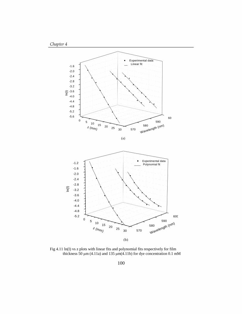
���������
100
Fig 4.11 ln(I) vs z plots with linear fits and polynomial fits respectively for film thickness 50 �m (4.11a) and 135 �m(4.11b) for dye concentration 0.1 mM
0 5 10 15 20 25 30
-5.6
-5.2
-4.8
-4.4
-4.0
-3.6
-3.2
-2.8
-2.4
-2.0
-1.6
570580
590600
(a)
Experimental data Linear fit
Wavelength (nm)
ln( I)
z (mm)
0 5 10 1520
2530
-5.2
-4.8
-4.4
-4.0
-3.6
-3.2
-2.8
-2.4
-2.0
-1.6
-1.2
570
580590
600
(b)
Experimental data Polynomial fit
Wavelength (nm)
ln(I)
z (mm)

� ����������������������������������������������������������������� �����������
101
For higher dye concentrations, irrespective of film thickness, the observed data
on fluorescence emission as a function of z shows a good match with equation
(4.8), supporting the existence of a space dependent attenuation coefficient. Fig
4.10 shows the experimental data fitted with a 2nd degree polynomial in z for
wavelengths 590nm, 600nm and 610 nm for waveguide thickness 50 microns and
at a dye concentration 1mM .
.
05
1015
2025
30
-5.2
-4.8
-4.4
-4.0
-3.6
-3.2
-2.8
-2.4
-2.0
-1.6
-1.2
580590
600610
620
Experimental data Polynomial fit
Wavelength (nm)
Ln(I)
z (mm)
Fig 4.10 Polynomial fit for ln(I) vs z plots for 50 µ m thick waveguide with dye concentration 1mM
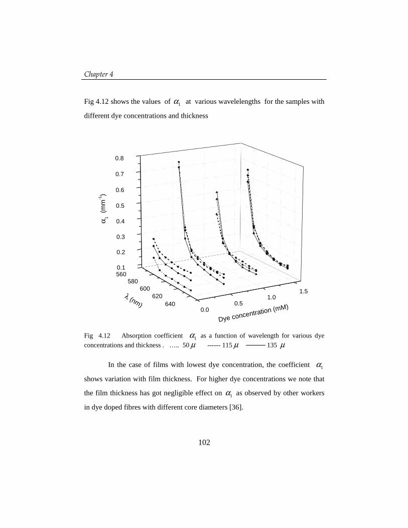
���������
102
Fig 4.12 shows the values of 1α at various wavelelengths for the samples with
different dye concentrations and thickness
560580
600620
640
0.1
0.2
0.3
0.4
0.5
0.6
0.7
0.8
0.00.5
1.01.5
α 1 (m
m-1)
Dye concentration (mM)
λ (nm)
Fig 4.12 Absorption coefficient 1α as a function of wavelength for various dye concentrations and thickness . ….. 50 µ ------ 115 µ 135 µ
In the case of films with lowest dye concentration, the coefficient 1α
shows variation with film thickness. For higher dye concentrations we note that
the film thickness has got negligible effect on 1α as observed by other workers
in dye doped fibres with different core diameters [36].

� ����������������������������������������������������������������� �����������
103
Fig 4.13 shows the variation of 2α with wavelength for various dye
concentrations and thickness . Note that for film with dye concentration 0.1 mM
and thickness 50 µ m, 1α α≅ .
560580
600620
640
0.000
0.003
0.006
0.009
0.012
0.015
0.018
0.00.5
1.01.5
-α2 (m
m-2)
Dye concentration (mM)λ (nm)
Fig 4.13 Space dependent term of absorption coefficient 2α as a function of wavelength for various dye concentrations and thickness . …... 50 µ ------ 115 µ 135 µ Thus we see that, for dye doped waveguides – especially when there is an
overlap between the absorption and emission bands – the attenuation cannot be
fully defined by the usual Beer-Lambert’s law. Due to several complex

���������
104
interactions between the dye molecules and the propagating light, the attenuation
coefficient gets modified with propagation distance and hence can be expressed
as a function of propagation distance. In such waveguides, a space dependent
attenuation coefficient will explain the observed attenuation mechanisms
especially at higher dye concentrations.
4.6 Conclusions
In this chapter, we have discussed the fabrication and characterization of
rhodamine 6G doped polymethyl methacrylate film waveguides. The absorption
and front surface fluorescence emission of the fabricated films were recorded.
The attenuation in the waveguides was characterized by a non-destructive side
illumination fluorescence technique. We observed that the attenuation
mechanisms in a dye doped waveguide – especially for the dyes having an
overlap between the absorption and emission spectra – can be explained only
with a space dependent attenuation coefficient. In such cases, the transmitted
light will not strictly obey the conventional Beer-Lambert’s law.
References 1. P.P. Sorokin and J.R. Lankard, IBM J. Res Develop 10, 162-163 (1966). 2. B.H. Soffer, B.B. Mc Farland, Appl. Phys. Lett 10, 266-267 (1967). 3. O.G. Peterson, B.B. Snavely, Appl. Phys. Lett 12 (7), 238-240(1968). 4. A. Costela, I. Garcia-Moreno, J. M. Figuera, F. Amat-Gueria and R. Sastre,
Laser Chem. 18, 63-84 (1998). 5. A. Costela, I. Garcia-Moreno, C. Gomez, O. Garcia and R. Sastre, J. of Appl.
Phys 90(7), 3159-3166 (2001). 6. D. Lo, J.E. Parris, J.L. Lawless, Appl. Phys. B 55, 365-367 (1992). 7. Y. Sorek, R. Reisfeld, I. Finkelstein and S. Ruschin, Appl. Phys. Lett. 66(10),
1169-1171 (1995).
� ����������������������������������������������������������������� �����������
105
8. A. Costela, F. Florido, I. Garcia-Moreno, F. Amat-Guerri, J.M. Figuera and R. Sastre, Appl. Phys. B 60, 383-389 (1995).
9. F. Lopez Arbeloa, T. Lopez Arbeloa, I. Lopez Arbeloa, A. Costela, F. Florido, I. Garcia-Moreno, J.M. Figuera, F. Amat-Guerri and R. Sastre, Appl. Phys. B 64, 651-657 (1997).
10. A. Costela, I. Garcia-Moreno, J.M. Figuera, F. Amat-Guerri, R. Mallavia, M. D. Santa-Maria and R. Sastre, J. of Appl. Phys 80(6), 3167-3173 (1996).
11. Kwong-Cheong Yee, Teck-Yong Tou, Seik-Weng Ng, Appl. Opt 37(27), 6381-6385 (1998).
12. A.V. Deshpande and E.B. Namdas, Appl. Phys. B 64, 419-421 (1997). 13. Seong-Shan Yap, Wee-Ong Siew, Teck-Yong Tou and Seik-Weng Ng, Appl.
Opt 41(9), 1725-1728 (2002). 14. M.G. Kuzyk, D.W. Garvey, S.R. Vigil, D.J. Welker, Chemical Physics 245,.
533-544 (1999). 15. Mark G. Kuzyk, Dennis W. Garvey, Brian K. Canfield, Steven R. Vigil, David
J. Welker, Jeff Tostenrude, Chris Breckon, Chemical Physics 245, 327-340 (1999).
16. G. D. Peng, P.L. Chu, Z Xiong, T.W. Whitbread, R.P. Chaplin, J.Lightwave Technology 14(10), 2215-2223 (1996).
17. A. Tagaya, S. Teramoto, T. Yamamoto,K. Fujii, E. Nihei, Y. Koike, K. Sasaki, IEEE J.of Quantum Electronics, 31(12), 2215-2220 (1995).
18. Akihiro Tagaya, Shigehiro Teramoto, Eisuke Nihei, Keisuke Sasaki, Yasuhiro Koike, Appl. Optics 36(3), 572-578 (1997).
19. Vincent Dumarcher, Licinio Rocha, Christine Denis, Celine Fiorini, Jean- Michel Nunzi, Frank Sobel, Bouchta Sahraoui, Denis Gindre, J.Opt. A: Pure Appl. Opt 2, 279-283 (2000).
20. D.J. Welker, M.G. Kuzyk, Appl. Phys .Lett 69(13), 1835-36(1996). 21. R. J. Kruhlak, M.G. Kuzyk, J. Opt. Soc. Am. B 16(10), 1749-1755(1999). 22. K Geetha , M Rajesh, V P N Nampoori, C P G Vallabhan and P Radhakrishnan,
J. Opt. A: Pure Appl. Opt. 6 , 379–383 (2004). 23. Akihiro Tagaya, Shigehiro Teramoto, Elsuke Nihei, Keisuke Sasaki, Yasuhiro
Koike, Appl. Optics 36(3), 572-578(1997). 24. Ken Kuriki, Takeyuki Kobayashi, Nana Imai, Toshihiko Tamura, Susumu
Nishihara, Yukihisa Nishizawa, Akihiro Tagaya, Yasuhiro Koike, Yoshi Okamoto, Appl. Phys. Lett., 77(3), 331-333 (2000).
25. Xiao-lei Zhu, Dennis Lo, Appl. Phys. Lett, 80 (6) , 917-919 (2002). 26. Alexander Argyros, Martijn A. van Eijkelenborg, Stuart D. Jackson, Richard P.
Mildren, Opt. Lett 29(16) , 1882-1884 (2004). 27. F.P. Shäfer (Ed.), Dye Lasers, Topics in Applied Physics Volume 1, Springer-
Verlag, Berlin Heidelberg, 1990 28. F.L. Arbeloa, P.R. Ojeda, I.L. Arbeloa, J. Photochem. Photobio A 45, 313
(1988). 29. I.L. Arbeloa, J. Chem. Soc. Faraday Trans II 78, 989 (1982).

���������
106
30. D.W. Garwey, K. Zimmerman, P. Young, J. Tostenrude, J.S. Townsend, Z. Zhou, M. Lobel, M. Dayton, R. Wittorf and M.G. Kuzyk , J.Opt.Soc.Am.B 13(9), 2017-2023 (1996).
31. Toshikuni Kaino, J.Opt.A:ure Appl.Opt 2 ,R1-R7 (2000). 32. R.J. Kruhlak, M.G. Kuzyk, J.Opt.Soc.Am. B 16(10), 1756-1767 (1999). 33. E. De La Rosa-Cruz, C.W. Dirk, O. Rodriguez and V.M. Castano, Fiber and
Integrated Opt. 20(5), 457-464 (2001). 34. C. Koeppen, R.F. Shi, W.D. Chen, A.F. Garito, J. Opt. Soc. Am. B 15(2), 727-
739 (1998). 35. G. D. Peng, P.L. Chu, SMIREE, X. Lou, R.A. Chaplin, J. Electrical and
Electron. Engg, Australia-IE Aust & The IREE Society 15(3), 289-296 (1995). 36. Robert J. Kruhlak, Characterization of molecular excited states for nonlinear
optics , PhD Thesis, Washington State University (2000).

107
����������������
��������������� ������������������������������ ������������������������������ ������������������������������ �������������������������������������������������������������������������������������������������������
������������������������������� ����������������� � ������������ ������������������������ ������������������������� ������ �������� �� ����� ���������������� ����������������������� ��������� ��� ������ ������������ ������� �� ���� ������� ������� ����� ���� �������� ��� �� � ��� ��� �������� �������� � � � �������������� ���� �������� � �������������� ��� ������������������������ ���� ���������������������������������
5

����������������������������������������������������������������������������������� ����������������
109
5.1 Introduction
One of the fundamental quantities of importance for a laser medium
is its optical gain. Simple measurements of emission in highly excited
systems with gain are difficult to interpret since emission is geometry
dependent and not directly related to fundamental parameters. Under lasing
conditions, further complications are introduced by the coupling of molecular
emission to optical cavity modes. A useful and convenient method of
measuring gain is based on measurements of amplified spontaneous emission
(ASE). This technique was first demonstrated in 1970 by Silfvast and Deech
[1] for high gain pulsed metal vapour lasers. Shank et al modified this for
pulsed dye lasers [2]. ASE is a phenomenon where the spontaneously emitted
light gets amplified as it propagates along the gain medium and even without
the feedback of the emitted radiation.
In this chapter, we discuss our observation of ASE from dye doped
planar waveguide strucutures of various thicknesses and dye concentrations.
Gain characterization was done by a variable stripe length method widely
used for both organic and inorganic materials prepared in a slab geometry
[3,4]. The cross section of the pump beam was in the form of a stripe. The
optical gain in each sample is studied by the relation between the pump
length and ASE intensity. We also discuss the propagation characteristics of
ASE through the waveguide. This was done by shifting the position of the
excitation stripe in such a way that the ASE from the end of the pump stripe
is guided along different lengths of the waveguide.
For most dyes, the absorption and emission bands overlap and the
short wavelength fluorescence is reabsorbed. For such dyes the observed
fluorescence peak is shifted to longer wavelengths at higher concentrations.
Thus, wavelength tuning can be achieved by changing the dye concentration
[5]. Similar red-shift was observed for the spectra taken from transversely

����� �����
110
pumped dye-doped fibres and waveguides when the excitation spot
position was shifted along the length of the fibre/waveguide by translating
either the source or the waveguide [6-8]. Using a similar technique, we
investigated the wavelength tuning in a transversely pumped Rh6G doped
PMMA film waveguide by observing the wavelength changes of ASE.
5.2 Amplified Spontaneous Emission
Any gain medium can amplify not only the input field from a laser
oscillator or any other source, but also the spontaneous radiation emitted by
the excited molecules of the amplifier itself. The ASE cascade of emission
from dye molecules in the excited state is stimulated by the spontaneous
emission from other molecules' decay from an excited state. ASE is not, then,
a purely spontaneous phenomenon, but spontaneously emitted photons that
are amplified by further coherent stimulated emission. The emitted photons
will be of the same frequency centred around the wavelength of maximum
gain. In materials with high gain, the laser- like amplified spontaneous
emission (ASE) occurs without the aid of multiple pass gain build up in a
cavity with mirrors. It requires relatively high pump powers in the single pass
gain geometry. A signature of amplified spontaneous emission is gain
narrowing of the fluorescence spectrum. As the pump intensity increases the
spectrum changes from a normal fluorescence to pure ASE. The direction of
ASE is perpendicular to the direction of polarization of the incident
intensity.

����������������������������������������������������������������������������������� ����������������
111
5.3 Gain measurement
The ASE theory starts with a one dimensional approximation [3],
describing the rate of change of fluorescence intensity with length of the
pumped region as,
0dI
AP gIdz
= + ……(5.1)
where I - Fluorescence intensity propagating along the Z-axis.
0AP - Spontaneous emission proportional to pump intensity
g - net gain given by α−′g where g ′ is the gain due to stimulated
emission and α is the optical loss
l - length of the pumped region
The solution of eqn. (5.1) with respect to pump length is
( )0 exp 1l
API gl
g� �= −� � ……(5.2)
Shank et al [2 ] measured the single pass gain of dye laser by comparing the
intensities of ASE in single and double cell lengths. By writing an equation
similar to that of eqn. (5.2) for a pump stripe of length 2l , we get
( )02 exp 2 1l
API g l
g� �= −� � ……(5.3)
From equations (5.2) and (5.3), the net gain can be obtained as,
2
2ln 1l
l
Ig
l I
� �= −� �
� �� � … ..(5.4)
5.4 Experiment
Experiments were conducted on free standing thin films of poly
methyl methacrylate (PMMA) doped with Rhodamine 6G. Details of sample

����� �����
112
preparation are given in Chapter IV. We conducted experiments on films
with dye concentrations, 0.5 mM, 1mM and 1.5 mM. Experimental results
presented here are for samples with 50 µ m thickness, unless otherwise
specified. The samples were transversely pumped using 10ns pulses from a
frequency doubled Nd:YAG laser (532 nm, 10Hz). A set of calibrated
neutral density filters were used for varying the pump energy. The beam
was focused into a narrow stripe of approximately 50 microns width. The
stripe length was varied using an adjustable slit.
Fig 5. 1 Excitation and light collecting schemes
When ASE occurs in a long narrow stripe, most of the light is emitted
at the ends of the stripe. The emission from the sample was collected by a
fibre and directed to a 0.5 m spectrograph (SpectraPro-500i) coupled with a
cooled CCD array. The distance between the collecting fibre and the
waveguide edge was 1cm. A slit was kept infront of the fibre so that only the
axially confined modes are collected. The sample was kept on a translator so
fluorescence
Collecting fibre
z
NDF
Cylindrical lens
ASE
Spectrograph-CCD Assembly
Nd:YAG (532 nm)

����������������������������������������������������������������������������������� ����������������
113
as to enable horizontal shifting of the excitation stripe along the length of
the waveguide. We first placed the pump stripe right upto the edge of the film
(z=0) and recorded the emission spectra for various pump energies. Then the
stripe position was shifted, thereby varying z - the distance between one end
of the pump stripe and the observation edge of the film. (Fig 5.1)
Observations were made with excitation stripe lengths 2mm, 4mm and 6mm.
5.5 Results and Discussions
5.5.1 Observation of ASE
First we recorded the emission spectra for z=0, at various pump intensities
with a constant pump stripe of length 2mm. (fig 5.2).
Fig 5.2a : Emission from the waveguide edge for stripe length 2mm at various pump energies for a dye concentration 0.5 mM (a) 0.10 mJ/pulse (b) 0.31 mJ/pulse (c) 1 mJ/pulse (d) 9.1 mJ/pulse
500 520 540 560 580 600 620 640 660
0
2000
4000
6000
8000
10000
12000
F
d
c
b
a
Inte
nsity
(A
.U)
Wavelength (nm)

����� �����
114
480 500 520 540 560 580 600 620 640 660 680
0
10000
20000
30000
40000
F
a
b
c
Inte
nsity
(A.U
)
Wavelength (nm)
Fig 5.2b : Emission from the waveguide edge for stripe length 2mm at various pump energies for a dye concentration 1 mM (a) 0.7 mJ/pulse (b) 2.2 mJ/pulse (c) 6.4 mJ/pulse In the case of (a) the Y-axis is scaled by multiplying with 5
500 520 540 560 580 600 620 640 660
0
2000
4000
6000
8000
10000
F
c
b
a
Inte
nsity
(A.U
)
Wavelength (nm)
Fig 5.2c : Emission from the waveguide edge for stripe length 2mm at various pump energies for a dye concentration 1.5 mM (a) 0.126mJ/pulse (b) 0.4mJ/pulse (c) 1.26mJ/pulse
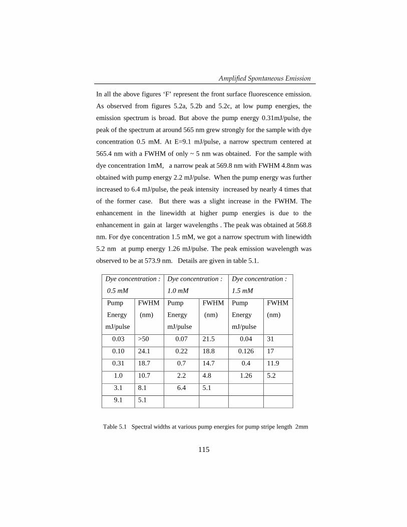
����������������������������������������������������������������������������������� ����������������
115
In all the above figures ‘F’ represent the front surface fluorescence emission.
As observed from figures 5.2a, 5.2b and 5.2c, at low pump energies, the
emission spectrum is broad. But above the pump energy 0.31mJ/pulse, the
peak of the spectrum at around 565 nm grew strongly for the sample with dye
concentration 0.5 mM. At E=9.1 mJ/pulse, a narrow spectrum centered at
565.4 nm with a FWHM of only ~ 5 nm was obtained. For the sample with
dye concentration 1mM, a narrow peak at 569.8 nm with FWHM 4.8nm was
obtained with pump energy 2.2 mJ/pulse. When the pump energy was further
increased to 6.4 mJ/pulse, the peak intensity increased by nearly 4 times that
of the former case. But there was a slight increase in the FWHM. The
enhancement in the linewidth at higher pump energies is due to the
enhancement in gain at larger wavelengths . The peak was obtained at 568.8
nm. For dye concentration 1.5 mM, we got a narrow spectrum with linewidth
5.2 nm at pump energy 1.26 mJ/pulse. The peak emission wavelength was
observed to be at 573.9 nm. Details are given in table 5.1.
Table 5.1 Spectral widths at various pump energies for pump stripe length 2mm
Dye concentration :
0.5 mM
Dye concentration :
1.0 mM
Dye concentration :
1.5 mM
Pump
Energy
mJ/pulse
FWHM
(nm)
Pump
Energy
mJ/pulse
FWHM
(nm)
Pump
Energy
mJ/pulse
FWHM
(nm)
0.03 >50 0.07 21.5 0.04 31
0.10 24.1 0.22 18.8 0.126 17
0.31 18.7 0.7 14.7 0.4 11.9
1.0 10.7 2.2 4.8 1.26 5.2
3.1 8.1 6.4 5.1
9.1 5.1

����� �����
116
Spectral narrowing of the emitted radiation can be due to several
reasons. A variable stripe length method was used to confirm whether the
phenomenon responsible for spectral narrowing is ASE. If ASE occurs,
spectra should be broad at short stripe lengths and should narrow as the
excitation length increases [4,9].
For all the 3 dye concentrations specified above, we recorded the
spectra for stripe lengths 2mm, 4mm and 6mm at various pump powers .
Figure 5.3 shows a representative plot for the dye concentration 0.5 mM.
Fig 5. 3. Spectral narrowing with increase in stripe length for various pump Energies ( Dye concentration : 0.5 mM )
550 560 570 580 590 600 610 620 6300
300
600
900
1200
1500
550 560 570 580 590 600 610 620 630
0
10000
20000
30000
40000
50000
60000
70000
550 560 570 580 590 600 610 620 630
0
10000
20000
30000
40000
50000
60000
70000
80000
90000
c
b
a
Inte
nsity
(A.U
)
Wavelength (nm)
E=0.031 mJ/pulse
(a) l=2mm (b) l=4mm (c) l=6mm
c
a
b
In
tens
ity (A
.U)
Wavelength(nm)
E=3.1 mJ/pulse
(a) l=2mm (b) l=4mm (c) l=6mm
c
b
a
Inte
nsity
(A.U
)
Wavelength (nm)
E=9.1mJ/pulse
(a) l=2mm (b) l=4mm (c) l=6mm

����������������������������������������������������������������������������������� ����������������
117
As the pump stripe length increased, the threshold moved to lower energies.
Also, for a given pump energy, the FWHM reduced when stripe length
increased from 2mm to 4mm. (see Table 5.2 ), with a slight shift in the peak
wavelength. We also see a slight increase in the linewidth with further
increase in stripe length, due to enhanced gain at longer wavelengths too.
Enhanced stripe length increases number of molecules interacting with the
pump beam. At higher stripe lengths, additional emission like T→T (triplet-
triplet) or between states of weakly fluorescing dimers may result into
enhanced FWHM.
Table 5.2. FWHM of spectral emission for various pump energies and beam stripe lengths
5.5.2 Gain measurement from ASE spectra
For g proportional to pump power, then for pump power such that
1g l−> , eqn. (5.2) indicates that the stimulated emission intensity will
increase exponentially. Below this input power, the intensity variation will
be less than exponential. This change in power dependence gives rise to a
characteristic break point in the output intensity as a function of input power
[3]. At the highest input powers, saturation occurs, since the amplified light
is large enough to deplete a significant fraction of excited states.
FWHM (nm) Dye
concentra-
tion (mM)
Pump
Energy
(mJ/pulse)
mml 2=
mml 4=
mml 6=
0.5 3.1 8.1 5. 6 2.5
1 0.22 18.8 3.6 6.2
1.5 0.4 11.9 5.4 6.1

����� �����
118
Figure 5.4 gives a typical plot showing the dependence of the light
intensity emitted from the edge, integrated over all wavelengths, on the pump
energy. The sample dye concentration was 1 mM .
Fig 5.4 . Total emission intensity integrated over all wavelengths vs pump energy for pump stripe lengths (a) 2mm (b) 4mm
Equation (5.4) applies only for pump powers upto the onset of saturation. The
gain was calculated for pump energies 0.31 mJ/pulse, 0.7 mJ/pulse and 0.4
mJ/pulse respectively for the samples with dye concentrations, 0.5 mM, 1.0
mM and 1.5 mM. Figure 5.5 shows the wavelength versus gain plots for 50
µ m thick waveguides with various dye concentrations. The wavelength for
maximum gain shifted to red as dye concentration was increased. We also
observe a wider gain band width for higher dye concentration.
0.0 0.5 1.0 1.5 2.0 2.5
0
30000
60000
90000
120000
150000
(b)
I out
(A.U
)
Iin (mJ/pulse)
0 1 2 3 4 5 6 7
0
50000
100000
150000
200000
(a)
I out (
A.U
)
Iin (mJ/pulse)

����������������������������������������������������������������������������������� ����������������
119
565 570 575 580 585 590 595
-4
-2
0
2
4
6
8
10
12
14
16
18
3
2
1
Gai
n (c
m-1)
Wavelength (nm)
1 ... 0.5 mM at 0.31mJ/pulse2 ... 1.0 mM at 0.7mJ/pulse3 ... 1.5 mM at 0.4mJ/pulse
Fig 5.5 Wavelength vs gain plots for various dye concentratins
.
We also studied the thickness dependence on the gain. (figure 5.6)
Fig 5.6 Wavelength vs gain plots for dye concentration 1mM at pump power 0.7mJ/pulse , for film thickness (a) 50 µ m (b) 115 µ m(c) 135 µ m
565 570 575 580 585 590
-8
-6
-4
-2
0
2
4
6
8
10
12
14
16
18
(c)
(b)
(a)
Gai
n (c
m-1)
Wavelength (nm)

����� �����
120
The maximum gain was obtained for the smallest thickness 50 µ m. At
higher thickness, the planar structure of the waveguide will be nearer to that
of bulk medium which will reduce the gain with respect to that of thin film
structure.
5.5.3 ASE propagation through the waveguide and wavelength tunability
It is well-known that by varying dye concentration, wavelength
tuning can be attained in dye lasers [5]. For rhodamine 6G, there is a spectral
region of overlap between the absorption and emission bands. As a result,
the short wavelength emission from the dye molecules gets absorbed by
themselves and is re-emitted at a longer wavelength. Due to this self-
absorption and re-emission process, the peak emission wavelength shows a
red-shift with increase in concentration [5]. This property is utilized in the
concentration dependent tuning of the emitted wavelength. Increasing the
pathlength through the dye doped sample is somewhat similar to an
increment in dye concentration. A similar redshift was observed when the
pathlength through the waveguide/fibre was increased [6-8].
When irradiated with a narrow stripe, the ASE will be maximum at
the stripe ends, along a transverse direction. We changed the position of the
excitation stripe by translating the waveguide horizontally across the exciting
beam. Now, the ASE emitted at the end of the stripe was made to traverse
through the sample. By shifting the position of the exciting stripe, we varied
the propagation length of the emission through the waveguide. Emitted light
was collected exactly in a similar manner for the case z=0. Fig 5.7 shows
the spectra obtained for various z values at a pump energy 9.1mJ/pulse for
various stripe lengths for a sample with dye concentration 0.5 mM.

����������������������������������������������������������������������������������� ����������������
121
550 560 570 580 590 600 610 620 630
0
10000
20000
30000
40000
50000
60000
70000
80000
90000
(c)
(b)
(a)
540 560 580 600 620 640
0
5000
10000
15000
20000
25000
30000
35000
40000
43
2
1
Inte
nsity
(A.U
)
wavelength (nm)
(b) (1)z=0(2)z=5 mm(3)z=10 mm(4)z=15 mm
540 560 580 600 620 640
0
2000
4000
6000
8000
10000
12000
14000
4
3
2
1
(a)
(1) z=0(2) z=5 mm(3) z=10 mm(4) z=15 mm
Inte
nsity
(A.U
)
wavelength (nm)
4
3
2
1
Inte
nsity
(A.U
)
wavelength (nm)
(c)
(1) z=0(2) z=5 mm(3) z=10 mm(4) z=15 mm
Fig 5. 7 Evolution of ASE as it is guided through various lengths through
the waveguide for stripe lengths (a) mml 2= (b) mml 4= (c) mml 6= for pump energy 9.1 mJ/pulse ( Dye concentration : 0.5 mM).

����� �����
122
We observed a red-shift of the emission peak with increase in length
of propagation. Even after propagation through the sample, we got a narrow
emission spectrum, especially for longer stripe lengths.
For a stripe length of 2mm, we got narrow emission peaked at
565.4 for propagation distances z=0 and at 577.2 nm for z=5mm. Thus the
peak wavelength could be tuned over 12 nm . The spectral width increased
from 5nm to 11nm when z changed from 0 to 5mm. For further propagation
lengths, the emission became broad and ASE character of the emission was
lost. With longer pump stripe lengths, we got narrow emission even for
z=15mm. ASE could be tuned from 566.6 to 585.4 and 568.1 to 586.1
for stripe lengths 4mm and 6mm respectively. The tunability range thus got
enhanced. A tunability of around 19 nm was obtained for stripe length of
4mm as z varied from 0 to 15mm. It should also be noted that during the
tuning the spectral width generally increased upto 16 nm. Table 5.3 shows
the details of wavelength tuning for a pump stripe of length 4mm, for 3
different dye concentrations.
Table 5.3 FWHM and peak wavelength for different ‘z’ values for a pump stripe length 4 mm
Dye
concentra-
tion (mM)
Pump
Energy
(mJ/pulse)
Varia-
tion in z
(mm)
Variation
in FWHM
(nm)
Tuning range
(nm)
Tunabi-
lity
(nm)
0.5 9.1 0-15 4.6 - 15.8 566.6 - 585.4 18.8
1 2.2 0-15 4.6 - 13.4 571.5 - 590.8 19.3
1.5 1.26 0-15 5.4 - 15.8 579.3 - 592.9 13.6

����������������������������������������������������������������������������������� ����������������
123
We note that maximum gain and tunability is obtained with dye
concentration 1mM. For an increased dye concentration (1.5 mM), the gain as
well as the tunability gets reduced. This can be attributed to the well-known
concentration quenching of fluorescence emission for dyes. From the
fluorescence emission spectra of these samples, we have observed quenching
of fluorescence emission from the film with dye concentration 1.5 mM. (see
fig 4.4a in Chapter 4). For the same sample we also observed that the
saturation behaviour of the redshift with propagation distance is pronounced.
(see fig 4.6b in Chapter 4).
Conventionally, wavelength tuning is achieved by the use of
distributed Bragg reflectors as coupling mirrors in resonant cavities [10]. In
external cavity solid state lasers, wide-range wavelength tuning has been
achieved by the use of grating as the dispersion element. A tunability of
around 53 nm was obtained with a multiple prism-grating solid state dye laser
where the gain medium was a rhodamine 6G (Rh6G) doped modified PMMA
with trapezoidal geometry [11]. Multimode lasing and wide band tuning in
sol-gel distributed feed back waveguide lasers have also been reported [12-
14]. In these lasers tuning was achieved either by varying the period of gain
modulation [12,13] or by varying the temperature of the gain medium,
thereby varying its refractive index [14]. By the first method, a tunability of
more than 30 nm was achieved. By the latter method, with a Rh6G doped sol-
gel silica waveguide, 17nm tunability was obtained by varying the
temperature from 210C to 580C while with Rh6G doped PMMA waveguide,
6nm tunability was obtained by varying temperature from 220C to 980C.
A technique for tuning the ASE wavelength by controlling the
waveguide thickness has been reported for conjugated polymer films [15] as
well as for dye-doped solid state waveguide[16]. A wide range tunability of
around 30 nm was observed in these two cases.

����� �����
124
The main advantage of the present technique is that no bulk optics
are used for tuning. By simultaneous spectral measurement from both ends of
the pumped waveguide for different positions of the pump stripe along the
waveguide, simultaneous tuning of dual wavelength emission can also be
achieved.
One of the important points to be noted is that the intensity at longer
wavelengths of the ASE got amplified on traversing through the waveguide.
Output intensity at shorter wavelengths showed the usual exponential
decrease. Fig 5.8 shows the variation of output intensity at different
wavelengths with propagation length through the waveguide.

����������������������������������������������������������������������������������� ����������������
125
0 5 10 15 20
0
3000
6000
9000
12000
(c)
(b)
(a)
λ=565 nm λ=570 nm λ=575 nm λ=580 nm
Em
issi
on In
tens
ity (A
.U)
z (mm)
0 5 10 15 200
1000
2000
3000
λ=585 nmλ=590 nmλ=595 nmλ=600 nmλ=615 nm
Em
issi
on In
tens
ity (A
.U)
z (mm)
0 5 10 15 20
0
6000
12000
18000
24000
30000 λ=565 nm λ=570 nm λ=575 nm
Em
issi
on In
tens
ity (A
.U)
z (mm)
0 5 10 15 200
3000
6000
9000
λ=585 nm λ=590 nm λ=595 nm λ=605 nm λ=615 nm
Em
issi
on In
tens
ity (A
.U)
z (mm)
0 5 10 15 20
0
9000
18000
27000
36000
45000
54000 λ=565 nm λ=570 nm λ=575 nm
Em
issi
on In
tens
ity (A
.U)
z (mm)
0 5 10 15 200
2000
4000
6000
8000
10000
12000
14000
λ=585 nm λ=590 nm λ=595 nm λ=600 nm λ=615 nm
Em
issi
on In
tens
ity (A
.U)
z (mm)
Fig. 5.8 Emitted power at various wavelengths vs propagation length through the waveguide for stripe lengths (a) mml 2= (b) mml 4= (c) mml 6= for pump energy 9.1 mJ/pulse

����� �����
126
As can be clearly seen from the figure, as the propagation distance z
increases, emission intensity showed enhancement in intensity in the long
wavelength region. This is due to the gain in the long wavelength region due
to reemission as well as due to gain achieved as the radiation is propagated
through the amplifying medium. Such emission enhancement became
prominent as the stripe length of the pump beam was increased. Increase in
the stripe length enhances the interaction length between the pump radiation
and the dye molecules. This will result in gain in the spectral emission in
addition to the gain due to reemission in the long wavelength region.
Propagation characteristics of emitted radiation through the waveguide
cannot be described by the usual Lambert-Beer law with single attenuation or
gain coefficient. Due to complex interactions between the radiation and dye
molecules in the gain media, one has to describe a space dependent
attenuation and gain coefficient.
5.5.4 Photostability
The analysis of the changes in the emission spectrum as a function
of irradiation time, gives information regarding the photostability of the
samples. The intensity of the ASE from the samples decreased with the
number of pump pulses in a far from linear fashion (see fig 5.9). The solid
lines are the best fits for the nonlinear curves. This type of behaviour was
explained to be due to complex photothermal mechanisms of dye degradation
[17,18].
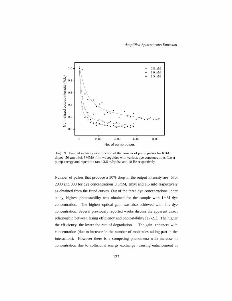
����������������������������������������������������������������������������������� ����������������
127
0 2000 4000 6000 8000
0.0
0.2
0.4
0.6
0.8
1.0
0.5 mM 1.0 mM 1.5 mM
Nor
mal
ised
out
put i
nten
sity
(A.U
)
No: of pump pulses
Fig 5.9 Emitted intensity as a function of the number of pump pulses for Rh6G doped 50 µm thick PMMA film waveguides with various dye concentrations. Laser pump energy and repetition rate : 3.6 mJ/pulse and 10 Hz respectively
Number of pulses that produce a 30% drop in the output intensity are 670,
2900 and 380 for dye concentrations 0.5mM, 1mM and 1.5 mM respectively
as obtained from the fitted curves. Out of the three dye concentrations under
study, highest photostability was obtained for the sample with 1mM dye
concentration. The highest optical gain was also achieved with this dye
concentration. Several previously reported works discuss the apparent direct
relationship between lasing efficiency and photostability [17-21]. The higher
the efficiency, the lower the rate of degradation. The gain enhances with
concentration (due to increase in the number of molecules taking part in the
interaction). However there is a competing phenomena with increase in
concentration due to collisional energy exchange causing enhancement in

����� �����
128
bleaching. This results into possible optimum concentration at which gain
and stability is maximum. In the present case, it is about 1mM.
5.7 Conclusions
We have characterized the gain in the dye doped planar waveguide structures
by ASE measurement technique. Measurements were done for samples with
dye concentrations 0.5mM, 1mM and 1.5 mM. Maximum gain (16.8 cm-1 at
573 nm) was obtained for a 50 µm thick waveguide with dye concentration
1mM. We have studied the propagation characteristics of amplified
spontaneous emission through the transversely pumped films. With increase
in propagation length through the waveguide, the emission peak showed a
red-shift due to self-absorption and re-emission by the dye molecules. As the
radiation propagated through the amplifying medium, spectrally narrow
output at longer wavelengths was obtained due to the gain achieved at these
wavelengths. Thus we could tune the ASE wavelength. The maximum
tunability obtained by this method was ~19 nm .
References 1. W.T. Silfvast, J.S. Deech, Appl. Phys. Lett 17, 97-99 (1970). 2. C. V. Shank, A. Dienes, W.T. Silfvast, Appl. Phys. Lett 17, 307-309 (1970). 3. K.L. Shaklee, R.F. Leheny, Appl. Phys. Lett 18 (11), 475-477 (1971). 4. Michael D. McGehee, Rahul Gupta, Siegfried Veenstra, E. Kirk Miller,
Maria A. Diaz-Garcia, Alan J. Heeger, Phys. Rev. B 58 (11), 7035-7039 (1998).
5. F.P. Shäfer (Ed.), Dye Lasers, Topics in Applied Physics Volume 1, Springer-Verlag, Berlin Heidelberg (1990).
6. R.J. Kruhlak, M.G. Kuzyk, Linear Optical Properties of Waveguides and Fibers, Proc. SPIE 3799, 312-319 (1999).
7. E. De La Rosa-Cruz, C.W. Dirk, O. Rodriguez and V.M. Castano, Fiber and Integrated Opt. 20(5), 457-464 (2001).
8. K. Geetha, M. Rajesh, C.P.G. Vallabhan, V. P.N. Nampoori and P. Radhakrishnan, J. Opt. A: Pure Appl. Opt. 6, 379-383 (2004).

����������������������������������������������������������������������������������� ����������������
129
9. Maria A. Diaz-Garcia, Susana Fernandez De Avila, Mark G. Kuzyk, Appl. Phys. Lett 80(24), 4486-4488 (2002).
10. J.E. Roman, K. A.Winick, Appl. Phys. Lett 61(23), 2744-2746 (1992). 11. Francisco. J. Duarte, Appl. Opt 38(30), 6347-6349 (1999). 12. Xiao-lei Zhu, Dennis Lo, Appl. Phys. Lett, 80(6) , 917-919 (2002). 13. Dennis Lo, Lei Shi, Jun Wang and Guo-Xuan Zhang, Appl. Phys. Lett
81(15), 2707-2709 (2002). 14. Xiao-lei Zhu, Dennis Lo, J.Opt. A: Pure Appl. Opt. 3, 225-228 (2001). 15. A. K. Sheridan, G.A. Turnbull, A.N. Safonov, I.D.W. Samuel, Phys. Rev. B
62(18), R11 929-R11 932 (2000). 16. Xiang Peng, Liying Liu, Jianfeng Wu, Yigang Li, Zhanjia Hou, Lei Xu,
Wencheng Wang, Fuming Li, Mingxin Ye, Opt. Lett 25(5), 314-316 (2000).
17. M.L. Ferrer, A.U. Acuna, F. Amat-Guerri, A. Costela, J.M. Figuera, F. Florido, R. Sastre, Appl. Optics 33, 2266 (1994).
18. A. Costela, I. Garcia-Moreno, J.M. Figuera, F. Amat-Guerri, J. Barroso, R. Sastre, Optics Commun. 130, 44-50 (1996).
19. F. Amat-Guerri, A. Costela, J.M. Figuera, F. Florido, R. Sastre, Chem. Phys. Lett. 209, 352 (1993).
20. A. Costela, F. Florido, I. Garcia-Moreno, R. Duchowicz, F. Amat-Guerri, J.M. Figuera, R. Sastre, Appl. Phys.B 60, 383 (1995).
21. A. Costela, I. Garcia-Moreno, J.M. Figuera, F. Amat-Guerri, R. Sastre, Appl. Phys.Lett. 68, 593-595 (1996).
131
������������������������������������������������������������ ��������� ��������� ��������� ������������������������������������������������������������������������������������������
����������������������������� ��� � �������� � ��� � ���� ���� ���������� ���������������������� �������������� ������������������� ������ ������������� ������� ��� � ����� ������� � ����� � ��� ���������� ���������� ��������������� ��������������� ��������������������������������� ����������� �� ��������������������������������� ������������������ ���������������������� �������������� �����������������!������������������������������ ��������������������
6

�������������������������������������������������������������������������������������������� ���������������
133
6.1 Introduction
Organic solid state lasers are attractive because of their wide
wavelength tunability and processing flexibility. There have been a lot of
investigations on organic polymer lasers with various organic material
systems such as dye-doped polymers [1-4] and conjugated polymers [5-9].
Laser emission from dye doped dendrimer and dendrimer doped polymers
has also been reported during the past few years [10-11]. Polymeric
materials in particular offer advantages such as ease of processing, which
permits fabrication of devices of virtually any shape and potentially very low
cost. Hence, dye doped polymers continue to attract researchers as promising
gain media for solid state lasers. The combination of the tunability and high
efficiency of laser dyes with the high power density that can be easily
achieved in waveguide structures make devices based on dye doped polymer
waveguides and fibres very promising [12-16]. Wide range tunable laser
emission have been reported from polymer thin films in optically pumped
distributed feedback scheme [12,17]. There have been numerous
investigations on laser emission from polymer planar microcavities [18,19]
and polymer micro-ring lasers as well [20-21].
This chapter describes the details of our work on multimode laser
emission from a transversely pumped free standing polymer film of
polymethyl methacrylate(PMMA) doped with the laser dye rhodamine 6G.
Since the film was freestanding – surrounded by air on both sides – the
reflections from the lateral faces of the sample provided the optical feedback
for laser action. This was evident from the lasing mode-spacing dependence
on the film thickness. The leaky mode emission from the film waveguide
showed a planar microcavity like behaviour due to Fabry-Perot effects.
Selective mode excitation was also observed with an increase in pump power.

��������
134
6.2 Energy level structure of dye molecule
Fig 6.1 Schematic representation of energy levels of an organic dye molecule
Figure 6.1 shows the relevant energy levels of an organic dye molecule such
as Rhodamine 6G [22,23]. State S0 is the ground state. S1 , S2 (Singlet) and
T1 ,T2 (Triplet) are excited electronic states. Singlet →Triplet or Triplet
→ Singlet transitions involve a spin flip and are far less likely to occur than
the transitions between two singlet or between two triplet states. Transitions
between two singlet states or between two triplet states which are spin
allowed, give rise to intense absorption and fluorescence. The characteristic
colour of organic dyes is due to S0 – S1 absorption and fluorescence
emission is due to S1 – S0 transition.
Abs
orpt
ion
Singlet states E
nerg
y
Em
issi
on
Exc
itatio
n
Abs
orpt
ion
S2
S1
S0
Triplet states
T2
T1 0υ
kυ

�������������������������������������������������������������������������������������������� ���������������
135
The typical energy separation such as S0 – S1 is about 20,000 cm-1.
The singlet and triplet states in turn are split further into vibrational levels.
Typical energy separation between two adjacent vibrational levels (shown as
dark horizontal lines in fig 6.1) within a given singlet or triplet state is about
1500cm-1. The fine splitting shown in the figure as lighter lines corresponds
to rotational levels, whose spacing is a few cm-1.
The pumping cycle of a dye laser can be described by a 4-level
system. At sufficiently high pump intensity, population inversion may be
achieved between the level 0υ in S1 and higher rovibronic levels kυ in S0,
which have a negligible population at room temperature due to small
Boltzmann factor )/)(exp( kTE kυ− . As soon as the gain on the transition
)()( 010 SS kυυ → exceeds the total losses, laser oscillation starts. The
lower level )( 0Skυ which now becomes populated by stimulated emission
from )( 10 Sυ is depleted very rapidly by collisional de-excitation to the
lowest level in S0.
Intersystem crossings between S1 and T1 levels will reduce the
fluorescence quantum efficiency of the laser dye. Presence of heavy metals
like Fe or groups like halides enhance such intersystem crossing and hence
will act as “killers” of fluorescence emission. Molecules such as oxygen or
cyclo-octotetraene (OCT) are often added to the dye solutions to quench the
triplet population.
6.3 Fabry-Perot Cavities
Fabry-Perot (F-P) cavity is an optical resonator formed by two partially
reflecting mirrors separated by a distance d and is the most commonly used
cavity for optical feedback in a laser device.

��������
136
The transmission spectrum of F-P cavity is the axial mode pattern
which contain peaks of equispaced frequency interval dc
2. A free standing
thin film can be modelled as a number of F-P cavities which are optically
coupled in series (fig 6.2). One can think of the higher modes as those
leaking out of the F-P structures.
Fig 6.2 Light propagation in planar waveguide represented by serially connected F-P etalons
6.4 Experimental setup
The experimental setup was the same as the one described in Chapter V
except for the difference in the light collecting scheme. Here no slit was
placed in between the film and the collecting fibre, so as to allow the
collection of the leaky rays from the surfaces of the waveguide (see fig 6.3).
(a) (b)
Fig 6.3 Diagrammatic representation of recording the leaky modes from planar waveguide using optical fibre (a) with slit to record the lower propagating modes only (b) without slit to record the complete mode pattern

�������������������������������������������������������������������������������������������� ���������������
137
The amplified spontaneous emission(ASE) threshold for the sample with 1.5
mM dye concentration was found to be 0.126 mJ/pulse for a pump stripe of
length 2mm. The threshold decreased for increased stripe lengths. The
emission from a 50 mµ thick sample having a dye concentration of 1.5 mM
was collected by varying the pump energy from 0.02 mJ/pulse to 1.82
mJ/pulse. The pump beam was focused into a narrow stripe of length 6mm
and approximately 50 microns width.
6.5 Results and Discussions
6.5.1 Observation of multimode emission
Figure 6.4 shows the emission spectra recorded for different points
of transverse excitation (z) at a pump energy 0.2mJ/pulse for a 50 mµ thick
film of dye concentration 1.5 mM pumped with a stripe of length 6 mm. The
distance between one end of the pump stripe and the observation edge of the
film was measured as ‘z’.
The spectrum shown in fig 6.4(b) clearly indicates the existence of
resonant modes. The average mode spacing is ~2.3 nm which agrees with the
axial mode spacing of F-P etalon of thickness 50 mµ . The strongest
emission lines at 576.5 nm and 578.8 nm had a FWHM ~ 0.6 nm. Such a
spectral narrowing is characteristic of laser emission.

��������
138
550 560 570 580 590 600 610 620 630
0
2000
4000
6000
8000
10000
12000
14000
16000
550 560 570 580 590 600 610 620 630
0
5000
10000
15000
20000
25000
550 560 570 580 590 600 610 620 630
0
500
1000
1500
2000
2500
3000
3500
550 560 570 580 590 600 610 620 6300
200
400
600
800
1000
1200
550 560 570 580 590 600 610 620 630 640 650 660 670
100
200
300
400
500
600
700
E
mis
sion
Inte
nsity
(A
.U)
wavelength (nm)
Em
issi
on In
tens
ity (
A.U
)
wavelength (nm)
(d)(c)
(b)(a)
Em
issi
on In
tens
ity (
A.U
)
wavelength (nm)
Em
issi
on In
tens
ity (
A.U
)
wavelength (nm)
(e)
Em
issi
on In
tens
ity (
A.U
)
wavelength (nm)
Fig 6.4. Emission spectra from a 50 mµ thick film at pump energy 0.2 mJ/pulse for (a) z=0 (b) z=5 mm (c) z=10 mm (d) z=15mm (e) z=20mm

�������������������������������������������������������������������������������������������� ���������������
139
Laser emission requires an external feedback. In our case, there were
no external mirrors to provide the feedback. Since the pumped polymer film
was a free standing one, the lateral faces of the film acted as mirrors giving
rise to a Fabry-Perot type optical cavity whose length corresponds to the film
thickness. Owing to the sample geometry and pumping scheme, the
longitudinal modes of this cavity form the transverse modes of the
waveguide. The axis of the F-P etalon is normal to the guiding direction of
light through the film. In the case of a thin stripe excitation, the stimulated
emission occurs in a direction along the stripe [6]. Both the stimulated
emission along with the propagation in the guiding gain medium and the
feedback at the lateral faces induce high gain for laser action, though
reflections at the lateral faces are much smaller than that of conventional
cavity mirrors. The fine structure pattern in the spectra shown in fig 2 can be
attributed to the axial modes of the Fabry Perot formed by two surfaces of the
planar waveguide. These modes are guided through the planar waveguide. In
other words the planar waveguide can be thought of as formed by a number
of serially connected F-P etalons. This can be verified from the mode
spacing.
The mode spacing at λ can be calculated using the equation which
describes Fabry-Perot cavities viz.,
nL2
2λλ =∆ … …(6.1)
where λ is the wavelength of the strongest emission line, n is the refractive
index and L is the length of the resonator cavity.
In the present case, the length of the Fabry Perot cavity corresponds
to the thickness of the film. Putting the values for n,λ and L as 576 nm,
1.49 and 50 mµ respectively, we get the mode spacing as 2.23 nm which is
the same as the observed value 2.3 nm within experimental error.

��������
140
The emission spectra for a film with same dye concentration, but
different thicknesses 115 mµ and 130 mµ taken for z=10mm are shown
in figure 6.5.
Fig 6.5. Emission from (a) 115 mµ (b) 130 mµ thick samples at pump energy 0.2 mJ/pulse and z=10 mm
580 600
0
1000
2000
3000
4000
5000
(b)
Em
issi
on In
tens
ity (A
.U)
wavelength (nm)
560 580 600 620
0
2000
4000
6000
8000
(a)
Em
issi
on In
tens
ity (A
.U)
wavelength (nm)

�������������������������������������������������������������������������������������������� ���������������
141
As expected, the line spacing for the 2 cases were smaller than the one for
sample thickness 50 mµ . For the 115 mµ thick sample the obtained mode
spacing is 1.25 nm and the calculated value was 0.99 nm. For the 130 mµ
thick sample, we got the mode spacing as 0.9 nm which is close to the
calculated value 0.86 nm. Thus the observed mode spacing agrees with the
calculated values. These observations confirm that the observed equally
spaced fine structures in the emission spectra are F-P type modes of the
optical cavity formed by the film thickness, which gets guided through the
film.
Similar phenomenon was observed by Yokoyama et al [11] in laser
dye doped dendrimer solution. The observed results can also be compared
with typical emission from Fabry-Perot micro-cavity lasers [24]. The F-P
like behaviour of asymmetric thin-film waveguide was explained to be quite
similar to that of thin-film microcavities [25] . The present case can be
considered as the F-P behaviour of a thick symmetric waveguide . The
reflections at film-air interface serve the purpose of metallic mirrors or
Bragg reflectors used in microcavity thin film lasers [18].
If we collect light by keeping a narrow slit in between the fibre and
the waveguide edge, these structures vanish. On placing a narrow slit, we
restrict the collection of light emission along the waveguide axis. In the
absence of slit, light emitted at different angles from the waveguide surface
can also be collected . Note that used a polymer optical fibre with 0.98 mm
core diameter and N.A 0.5 for collecting the emitted light. Hence the
observed emission can be considered as the leaky modes of the film
waveguide.
Leaky mode emission and microcavity like behaviour due to F-P
effect from asymmetric luminescent film waveguides has been studied
earlier [25]. The corresponding emission was tilted towards the substrate side
of the sample. The free standing polymer film in the present experiment was

��������
142
a symmetric waveguide, and the higher order transverse modes of the
waveguide leaked into air at different angles. The dependence of the peak
intensity and spectral width of the leaky mode self trapped exciton emission
on the observation direction has been studied in anatase thin films [26]. We
have also noticed that the intensity of the peaks depended on the collecting
angle.
The mode patterns were observed only when there was a separation
between one end of the pump stripe and the waveguide edge from which
emission was collected . As seen from fig 6.4, the emission spectra
comprises of equally spaced mode structures, superposed over the amplified
spontaneous emission (ASE). For z=0, when the pump stripe was placed
right upto the edge of the film, the mode structures were not prominent,
except for some weak structures superposed over the ASE. When z was
increased from 0, the emitted light was allowed to guide through the film so
that the effect of the F-P modes became predominant. Modes acquired
sufficient gain so that the mode structures became prominent. Now the
emission spectrum got broader and we get prominent mode structures over
the spectral range 560-600 nm(fig 6.4 b). Since the length of the unpumped
region increased with increasing z, eventually the intensity of the whole
emission together with the mode structures diminished. The propagation of
fluorescence as well as ASE in similar sample geometry and pumping
scheme has already been described in the previous chapters.
The collected spectrum contained both the stimulated emission and
ASE. We have noticed that the observed modes are the higher order
transverse modes (leaky modes) of the waveguide. For larger z, these modes
instead of propagating through the sample, leak out through the waveguide
surface. The modes which get propagated through the whole length of the
unpumped region undergo self-absorption and remission. Hence there is a
red-shift for the emitted light and for larger z, the ASE gets separated out of

�������������������������������������������������������������������������������������������� ���������������
143
the laser emission as is clear from fig 6.4(d) and fig 6.4(e). At higher pump
powers this is more evident.(Fig 6.6 and 6.7)
540 560 580 600 620 640 6600
200
400
600
800
1000
1200
(a)
Inte
nsity
(A.U
)
Wavelength (nm)
540 560 580 600 620 640 660
0
500
1000
1500
2000
2500
3000
3500
4000
4500
Inte
nsity
(A
.U)
Wavelength (nm)
540 560 580 600 620 640 660
0
1000
2000
3000
4000
5000
(c)
Inte
nsity
(A.U
)
Wavelength (nm)
Fig 6.6. Emission from 50 mµ thick film for z=15mm at pump energy (a) E=0.2 mJ/pulse (b) E=0.63 mJ/pulse (c) E=1.82 mJ/pulse.

��������
144
Fig 6.7. Emission from 50 mµ thick film for z=20mm at pump energy
(a) E=0.02 mJ/pulse (b) E=0.2 mJ/pulse (c) E=0.63 mJ/pulse (d) E=1.82 mJ/pulse.
Thus by the horizontal translation of the excitation stripe, thereby
varying z, we can separate out the laser emission and ASE. We also noticed
the emergence of mode strucutres over the redshifted ASE spectrum at pump
power 1.82 mJ/pulse for z=15mm and z=20mm(fig 6.6.c and 6.7 d). This
suggests that further increase in pump power could lead to prominent mode
structures over the redshifted ASE spectrum.
540 560 580 600 620 640 660
100
200
300
400
500
600
(a)
Inte
nsity
(A.U
)
Wavelength (nm)540 560 580 600 620 640 660
0
200
400
600
800
1000
1200
1400
1600
1800
(b)
Inte
nsity
(A
.U)
Wavelength (nm)
540 560 580 600 620 640 660
0
500
1000
1500
2000
2500
3000
3500
(c)
Inte
nsity
(A
.U)
Wavelength (nm)
540 560 580 600 620 640 660
0
1000
2000
3000
4000
5000
6000
(d)
Inte
nsity
(A.U
)
wavelength (nm)

�������������������������������������������������������������������������������������������� ���������������
145
6.5.2 Selective mode excitation
On increasing the pump energy, a selective excitation of laser mode was
observed. Figure 6.8 shows the emission spectrum at z=5mm recorded for
various pump powers. We observed that as the pump power was increased,
the centre lines of the spectrum gained more energy. Though there was an
increase in intensity for the whole emission, it is clear from the figures that
energy from other modes got coupled to the high gain mode at 576.5 nm as
the pump power was increased.
Fig 6.8 Emission from 50 mµ thick film for z=5mm at pump energy (a) E=0.02 mJ/pulse (b) E=0.2 mJ/pulse (c) E=0.63 mJ/pulse (d) E=1.82 mJ/pulse. For (c) and (d) the Y-axis values should be multiplied by a factor of 102
560 580 600
0
500
1000
1500
2000
2500
3000
(a)
Em
issi
on In
tens
ity (
A.U
)
wavelength (nm)560 580 600
0
5000
10000
15000
20000
25000
(b)
Em
issi
on In
tens
ity (A
.U)
wavelength (nm)
560 580 6000
200
400
600
800
1000
1200
(c)
Em
issi
on In
tens
ity (A
.U)
wavelength (nm) 560 580 6000
200
400
600
800
1000
1200
1400
1600
1800
(d)
Em
issi
on In
tens
ity (A
.U)
wavelength (nm)

��������
146
540 560 580 600 620 6400
200
400
600
800
1000
1200
1400
(a)
Inte
nsity
(A.U
)
Wavelength (nm)
540 560 580 600-5000
0
5000
10000
15000
20000
25000
30000
35000
(b)In
tens
ity (A
.U)
Wavelength (nm)
540 560 580 600-5000
0
5000
10000
15000
20000
25000
30000
35000
40000
(c)
Inte
nsity
(A
.U)
Wavelength (nm)
The output intensity was very high for pump energies 0.63 mJ/pulse and
1.82 mJ/pulse. To avoid the saturation of the CCD sensor, we placed neutral
density filter (with OD =2) just infront of the slit of the CCD. The intensity
of the mode at 571.5 nm shoots up when the pump energy reaches 1.82
mJ/pulse and the line width is reduced to ~0.4 nm.
Fig 6.9 shows a similar behaviour observed in the case of spectra
recorded for a film with dye concentration 1 mM and thickness 50 mµ
excited with a pump stripe of length 2mm and z=10mm.
Fig 6.9 Emission from 50 mµ thick film with dye concentration 1 mM for z=10mm at pump energy (a) E=0.07 mJ/pulse (b) E=0.7 mJ/pulse (c) E=2.2 mJ/pulse

�������������������������������������������������������������������������������������������� ���������������
147
We observe that the ASE background is negligibly small. The mode at
570.1nm shoots up for the pump energy 0.7mJ/pulse with FWHM as small
as 0.3 nm.
The mode competition can be clearly seen from fig 6.10.
Fig 6.10 Mode competition at various pump energies
6.6 Conclusions
A compact solid state laser based on dye doped polymer is demonstrated .
Laser emission was observed from a transversely pumped free standing poly
methyl methacrylate film doped with rhodamine 6G . The film was 50 mµ
560 562 564 566 568 570 572 574 576 578 580
0
5000
10000
15000
20000
25000
30000
35000
40000 E=0.07 mJ/pulse E=0.7 mJ/pulse E=2.2 mJ/pulse
Inte
nsity
(A.U
)
Wavelength (nm)

��������
148
thick with dimension 4cm x 2 cm. Reflections from the lateral faces
provided the optical feedback. This together with the guidance through the
gain medium gave rise to intense narrow emission lines. For the waveguide
with dye concentration 1.5 mM, an intense line with FWHM ~ 0.4 nm was
observed at 576.5 nm due to energy transfer from other modes. For dye
concentration 1mM, narrow emission at 570.1nm was observed with
linewidth 0.3 nm. The ASE was easily tuned by changing the point of
pumping on the waveguide structure thereby separating the lasing modes
from the ASE.
References
1. B.H. Soffer, B.B. Mc Farland, Appl.Phys.Lett 10, 266-267 (1967). 2. O.G. Peterson, B.B. Snavely, Appl. Phys. Lett 12 (7), 238-240(1968). 3. A. Costela, I. Garcia-Moreno, J.M.Figuera, F. Amat-Gueria and R. Sastre,
Laser Chem. 18, 63-84 (1998). 4. A. Costela, I. Garcia-Moreno, C.Gomez, O. Garcia and R. Sastre, J. of Appl.
Phys,90(7), 3159-3166 (2001). 5. Michael D. McGehee, Rahul Gupta, Siegfried Veenstra, E. Kirk Miller,
Maria A. Diaz-Garcia, Alan J. Heeger, Phys. Rev. B 58 (11), 7035-7039 (1998).
6. S.V. Frolov, Z.V. Vardeny, K. Yoshino, A. Zakhidov, R.H. Baughman, Phys. Rev. B 59 (8), R5284-R5287 (1999).
7. George Heliotis, Donal D.C. Bradley, Graham A. Turnbull, Ifor D.W. Samuel, Appl. Phys. Lett 81 (3) , 415-417 (2002).
8. M. Fakis, I. Polyzos, G. Tsigaridas, V. Giannetas , P. Persephonis, I. Spiliopoulos, J. Mikroyannidis, Phys. Rev. B 65 (19), 195203-1 – 195203-7 (2002).
9. Fumitome Hide, Maria A. Diaz-Garcia, Benjamin J. Schwartz, Mats R. Andersson, Qibing Pei, Alan J. Heeger, Science 273, 1833-1836 (1996).
10. Akira Otomo, Shiyoshi Yokoyama, Tatsuo Nakahama, Shinro Mashiko, Appl. Phys. Lett 77 (24), 3881-3883 (2000).
11. Shiyoshi Yokoyama, Akiro Otamo, Shinro Mashiko, Appl. Phys. Lett 80(1), 7-9(2002).
12. Vincent Dumarcher, Licinio Rocha, Christine Denis, Celine Fiorini, Jean- Michel Nunzi, Frank Sobel, Bouchta Sahraoui, Denis Gindre, J.Opt. A: Pure Appl. Opt 2, 279-283 (2000).
13. G. D. Peng, P.L. Chu, Z Xiong, T.W. Whitbread, R.P. Chaplin, J.Lightwave Technology 14(10), 2215-2223(1996).

�������������������������������������������������������������������������������������������� ���������������
149
14. Akihiro Tagaya, Shigehiro Teramoto, Eisuke Nihei, Keisuke Sasaki, Yasuhiro Koike, Applied Optics 36(3), 572-578 (1997).
15. Takeyuki Kobayashi, Werner J. Blau, Opt. Lett 26 (24), 1952-1954 (2001). 16. M. Karimi, N. Granpayeh, M.K. Morraveg Farshi, Appl. Phys B 78 , 387-
396 (2004). 17. F. Sobel, D. Gindre, J.M. Nunzi, C. Denis, V. Dumarcher, C. Fiorini-
Debuisschert, K.P. Kretsch, L. Rocha, Opt. Mat 27, 199-201(2004). 18. N. Tessler, G.J. Denton, R.H. Friend, Nature 382(22), 695-697(1996). 19. H. Becker, R.H. Friend, T. D. Wilkinson, Appl. Phys. Lett 72(11), 1266-
1268(1998). 20. M. Kuwata-Gonokami, R.H. Jordan, A. Dobalapur, H.E. Katz,
M.L.Schilling and R.E. Slusher, Opt. Lett 20(20), 2093-2095(1995). 21. S.V. Frolov, Z.V. Vardeny, K. Yoshino, Appl. Phys. Lett 72(15), 1802-1804,
1998. 22. A. Yariv, Optical Electronics 4th Edn., Saunders College Publishing, USA
(1991). 23. W. Demtröder, Laser Spectroscopy 3rd Edn., Springer Veralg, Berlin (1996). 24. R.C. Polson, G. Levina, Z.V. Vardeny, Appl. Phys. Lett 76(26),3858-
3860(2000). 25. A. Penzkofer, W. holzer, H. Tillmann, H.H. Horhold, Optics
Communications 229, 279-290(2004). 26. V. Kiisk, I. Sildos, A. Suisalu, J. Aarik, Thin Solid films 400, 130-
133(2001).

151
�������������������� ��� �������������������� ��� �������������������� ��� �������������������� ��� ������������
������������������ ��������� � ���� �������� ���� ���� �������������������������������������������
7

��������������������������������������������������������������������������������������������������������������������������
153
7.1 General Conclusions
The previous six chapters in this thesis present the design and fabrication of
photonic devices using polymer optical fibres and polymer waveguides.
Polymer optical fibres owing to their large diameter, large numerical
aperture, flexibility and geometrical versatility have attracted much research
interest in the field of optical sensing. One of the new techniques in the design of
fibre optic sensors is the usage of side polished fibres. Side polished polymer
optical fibres have been successfully employed for the fabrication of compact
sensors for measuring refractive index and absorption. The sensor performance
and methods for the enhancement in the performance were studied numerically
and accordingly the experiments were designed. A refractometer with wide
dynamic range and a sensor for measuring chemical reaction kinetics were
fabricated and characterized.
Dye doped polymer waveguides and fibres are potential candidates for
solid state gain media. High power and high gain optical amplification in organic
dye-doped polymer waveguides is possible due to extremely large emission cross
sections of dyes. We have fabricated free standing film waveguides of
rhodamine 6G doped poly methylmethacrylate, by double doctor blade tape
casting technique. Optical loss characterization for films with various thickness
and dye concentration was done by a non-destructive side illumination
fluorescence technique. The experimental observations clearly indicated a space
dependent attenuation coefficient.
The observation of amplified spontaneous emission (ASE) from these
samples and the characterization of optical gain are also discussed. The

������ �
154
propagation characteristics of ASE through the films were studied. A new
method for tuning the ASE wavelength was demonstrated by which a maximum
tunability of 19 nm was achieved.
Multimode laser emission based on leaky mode propagation
from these free standing film waveguide was one important study. The edge
emitted spectrum clearly indicated the existence of periodic resonant modes.
The reflections from the lateral faces of the free standing film provided the
optical feedback thus giving rise to a Fabry-Perot like optical cavity. This
together with the guidance through the gain medium gave rise to intense narrow
emission lines with line width ~0.3 nm .
7.2 Looking Forward
Though fibre optic sensors have many advantages over their
conventional bulk counterparts, from the applicability viewpoint, more attention
should be paid over certain key parameters such as cost, size and sensitivity.
Novel fabrication techniques, well suited for industrialization, have to be
developed. Numerical methods need to be used for designing and optimizing
these devices. Single mode side polished fibre components with metallic coatings
can be designed for sensors, couplers, filters and polarisers. Sensors and optical
amplifiers based on dye doped polymer fibres could be developed. Work in this
direction has already started in our lab.
Studies using picosecond pump source will be useful to understand fast
optical processes taking place in the dye doped media especially due to
intersystem and intrasystem crossings.

��������������������������������������������������������������������������������������������������������������������������
155
The demand for photonic devices that meet both performance criteria and
economic requirements has opened the door for novel technologies such as
polymer photonics. Development of novel solid-state lasing media such as
highly luminescent conjugated polymers opens up new possibilities for
applications and technologies. In contrast to other organic chromophores, they
suffer little concentration quenching.
New designs of compact laser sources could be taken up. Microcavity
lasers is a novel approach to lasing action in optically pumped organic solids.