
Design, fabrication and characterization of a Far-ï¬eld Superlens
6
Solid State Communications 146 (2008) 202–207 www.elsevier.com/locate/ssc Design, fabrication and characterization of a Far-field Superlens Hyesog Lee, Zhaowei Liu, Yi Xiong, Cheng Sun, Xiang Zhang * NSF Nanoscale Science and Engineering Center (NSEC), 5130 Etcheverry Hall, University of California, Berkeley, CA 94720, United States Received 25 May 2007; received in revised form 3 October 2007; accepted 15 October 2007 by the Guest Editors Available online 13 February 2008 Abstract The fabrication process as well as the optical characterization of a Far-field Superlens (FSL) is presented in detail. A FSL is capable of optically imaging well below the diffraction limit and works by enhancing and scattering evanescent waves to the far field which is then used to numerically reconstruct the object image [S. Durant, J. Opt. Soc. Am. B. 23(2006) 2383; Z. Liu, S. Durant, H. Lee, Y. Pikus, N. Fang, Y. Xiong, C. Sun, X. Zhang, Nano Lett. 7 (2007) 403]. We demonstrate the resolution of 70 nm gap distance of a three-line object in the far field. Also, a full optical imaging scheme, without the need for numerical processing, for a direct real-time subdiffraction-limited imaging is presented. Such remarkable imaging capability of FSL will revolutionize the optical imaging technique in the field of bio-imaging and nanolithography. c 2008 Elsevier Ltd. All rights reserved. PACS: 42.30.Va; 42.79.Bh; 42.79.Dj; 42.82.Bq Keywords: A. Nanostructures; B. Nanofabrications; D. Optical properties 1. Introduction Optical microscopy is the most widely used imaging method in modern scientific research. Nevertheless, conventional lens optics systems have fundamental limitations on how small a feature size can be resolved. Abbe discovered this physical barrier called “diffraction limit” a century ago [3]; even with an ideal optics system, the smallest resolvable feature is in the order of half of the wavelength used for imaging. As an object scatters incident illumination, one type of the scattered waves propagates to the far field hence it is called the ‘propagating wave’, but another type decays away near the object, which is called the ‘evanescent wave’. This evanescent wave contains high spatial frequency information that defines smaller features, but since it stays only in the near field, any far-field lenses suffer from the same diffraction limit. Numerous efforts to overcome the diffraction limit led to breakthroughs that had or will have lasting impacts in the field of optical imaging. Near-field scanning optical microscopy (NSOM) brings a tapered optical fibre tip close * Corresponding author. Fax: +1 510 643 2311. E-mail address: [email protected] (X. Zhang). to an object and scans the region of interest pixel by pixel, delivering the evanescent information to the far field through a fiber channel [4]. Stimulated emission depletion (STED) method utilizes the nonlinear response of fluorescent dyes to create an illuminating spot smaller than the diffraction limit [5]. These methods share the serial imaging method which tends to be quite slow and requires complex illumination and detection schemes. Hyperlensing, a promising parallel imaging technique, was first experimentally demonstrated by the authors. Even though the current hyperlens showed only one-dimensional (1D) resolution improvement, there are no theoretical limitations to realizing a hyperlensing with truly two-dimensional (2D) nanoimaging in the near future [6]. Another remarkable new concept of achieving high resolution optical imaging was proposed by Pendry [7]; Evanescent fields are enhanced by a thin slab of negative refractive index material, which recovers finer details of an object and produces a perfect image. It is an unprecedented parallel imaging method with the ability to bring even the evanescent portion of the wave into focus at the image plane, collecting all spatial information of the object. Recent experimental results provided strong proofs to such controversial theory, showing an image resolution far below the diffraction limit using a flat silver slab superlens [8–10]. 0038-1098/$ - see front matter c 2008 Elsevier Ltd. All rights reserved. doi:10.1016/j.ssc.2007.10.043
Transcript of Design, fabrication and characterization of a Far-ï¬eld Superlens

Solid State Communications 146 (2008) 202–207www.elsevier.com/locate/ssc
Design, fabrication and characterization of a Far-field Superlens
Hyesog Lee, Zhaowei Liu, Yi Xiong, Cheng Sun, Xiang Zhang∗
NSF Nanoscale Science and Engineering Center (NSEC), 5130 Etcheverry Hall, University of California, Berkeley, CA 94720, United States
Received 25 May 2007; received in revised form 3 October 2007; accepted 15 October 2007 by the Guest EditorsAvailable online 13 February 2008
Abstract
The fabrication process as well as the optical characterization of a Far-field Superlens (FSL) is presented in detail. A FSL is capable of opticallyimaging well below the diffraction limit and works by enhancing and scattering evanescent waves to the far field which is then used to numericallyreconstruct the object image [S. Durant, J. Opt. Soc. Am. B. 23(2006) 2383; Z. Liu, S. Durant, H. Lee, Y. Pikus, N. Fang, Y. Xiong, C. Sun, X.Zhang, Nano Lett. 7 (2007) 403]. We demonstrate the resolution of 70 nm gap distance of a three-line object in the far field. Also, a full opticalimaging scheme, without the need for numerical processing, for a direct real-time subdiffraction-limited imaging is presented. Such remarkableimaging capability of FSL will revolutionize the optical imaging technique in the field of bio-imaging and nanolithography.c© 2008 Elsevier Ltd. All rights reserved.
PACS: 42.30.Va; 42.79.Bh; 42.79.Dj; 42.82.Bq
Keywords: A. Nanostructures; B. Nanofabrications; D. Optical properties
1. Introduction
Optical microscopy is the most widely used imaging methodin modern scientific research. Nevertheless, conventional lensoptics systems have fundamental limitations on how small afeature size can be resolved. Abbe discovered this physicalbarrier called “diffraction limit” a century ago [3]; even withan ideal optics system, the smallest resolvable feature is in theorder of half of the wavelength used for imaging. As an objectscatters incident illumination, one type of the scattered wavespropagates to the far field hence it is called the ‘propagatingwave’, but another type decays away near the object, which iscalled the ‘evanescent wave’. This evanescent wave containshigh spatial frequency information that defines smaller features,but since it stays only in the near field, any far-field lenses sufferfrom the same diffraction limit.
Numerous efforts to overcome the diffraction limit ledto breakthroughs that had or will have lasting impacts inthe field of optical imaging. Near-field scanning opticalmicroscopy (NSOM) brings a tapered optical fibre tip close
∗ Corresponding author. Fax: +1 510 643 2311.E-mail address: [email protected] (X. Zhang).
0038-1098/$ - see front matter c© 2008 Elsevier Ltd. All rights reserved.doi:10.1016/j.ssc.2007.10.043
to an object and scans the region of interest pixel by pixel,delivering the evanescent information to the far field througha fiber channel [4]. Stimulated emission depletion (STED)method utilizes the nonlinear response of fluorescent dyesto create an illuminating spot smaller than the diffractionlimit [5]. These methods share the serial imaging methodwhich tends to be quite slow and requires complex illuminationand detection schemes. Hyperlensing, a promising parallelimaging technique, was first experimentally demonstrated bythe authors. Even though the current hyperlens showed onlyone-dimensional (1D) resolution improvement, there are notheoretical limitations to realizing a hyperlensing with trulytwo-dimensional (2D) nanoimaging in the near future [6].
Another remarkable new concept of achieving highresolution optical imaging was proposed by Pendry [7];Evanescent fields are enhanced by a thin slab of negativerefractive index material, which recovers finer details of anobject and produces a perfect image. It is an unprecedentedparallel imaging method with the ability to bring eventhe evanescent portion of the wave into focus at theimage plane, collecting all spatial information of the object.Recent experimental results provided strong proofs to suchcontroversial theory, showing an image resolution far belowthe diffraction limit using a flat silver slab superlens [8–10].

H. Lee et al. / Solid State Communications 146 (2008) 202–207 203
Fig. 1. Principle of FSL (Far-field SuperLens). (a) Definition of the propagating ([−nk0 nk0]) and the evanescent region ((−∞ ∼ nk0] and [nk0 ∼ ∞)) representedin 1D Fourier space (x axis) for simplicity. Vertical axis represents relative transfer coefficient(a.u) (b) Evanescent bands P1[k1 k2] and P2[−k2 − k1] selected bythe designed optical transfer function of a FSL are shifted into the propagating bands (c) using periodic grating structure for far-field detection. (d) Evanescent bandsP1 and P2 are shifted back into their original locations. (e) Information from (d) is combined with the propagating band from an additional measurement for imagereconstruction.
Later, another experiment at a longer wavelength with a siliconcarbide superlens also reported similar results [11]. A majordrawback of the superlensing is that it is still a near-fieldimaging technique [12]; The high resolution image is stillconfined to the proximity of the superlens surface [1].
The significance of recently proposed Far-field Superlens(FSL) theory is that it combines both of the superlensingand the far-field imaging ability, being able to image withsubdiffraction-limited resolution even in the far field [1].This direct far-field imaging became possible through a sub-wavelength grating that adds scattering functionality to thenear-field superlens. This grating is specially designed suchthat the retrieval of the original evanescent information ispossible from the far-field signal [1]. Immediately followingthe theoretical development, the first working FSL wasexperimentally demonstrated [2]. A line-pair object with50 nm linewidth and 120 nm centre-to-centre distance wassuccessfully imaged and resolved at half a metre away. Suchachievement opened a door to a real-time far-field imaging withnanoscale resolution.
We present a detailed account of the fabrication and thecharacterization of a FSL. In Section 2, the design of theFSL is presented which is followed by a detailed report onits fabrication process in Section 3. In Section 4, the far-field detection scheme is presented, and the actual opticalmeasurement and a imaging result are discussed in Section 5.
2. Far-field superlens design
When an object scatters incident light, the scattered wavescarry spatial information of the object image. The maximum
resolution of an imaging system is determined by the largestplanar wave vector collected at the image plane.
Fig. 1 schematically shows the principle of the FSL theoryin a nutshell. The horizontal axis represents the inplane spatialfrequency (wave vector) of the scattered waves by an object. Forsimplicity, only 1D coordinate is used. The vertical axis showsrelative intensity level in arbitrary unit. The band bounded by[−nk0, nk0], where n is the refractive index of the surroundingmedium and k0 = 2π/λ (λ is the wavelength in free space), isthe propagating band (Fig. 1(a)) and accessible by conventionaloptics. However, the waves in the evanescent band (Fig. 1(a))with larger wave vectors (i.e. carries finer spatial informationof the object) tend to decay away and are accessible only in thenear field [8–11].
A FSL is able to select a certain evanescent bands, forinstance, P1[k1 k2] and P2[−k2 − k1] in Fig. 1(b) according tothe designed optical transfer function (OTF) [1,2], and to shiftthem into the propagating region so that they can be detectedin the far field (Fig. 1(c)). It is well known in optics thatperiodic structures can provide additional planar momentumto interacting electromagnetic waves. Therefore, a speciallydesigned grating structure in a FSL provides just enoughmomentum to move the selected bands to the propagatingregion. Once the information is collected in the far field,those bands can be shifted back to their original positionsthrough numerical processes (Fig. 1(d)), and by combiningwith normally attainable propagating information (Fig. 1(e)),an image with much higher resolution can be reconstructed.It should be noted that the retrieved bands are not continuouswith the propagating band. However, applying a grazing angleincident light or a structured illumination [13] can close suchgaps, and even without such methods, it is reported that

204 H. Lee et al. / Solid State Communications 146 (2008) 202–207
Fig. 2. (a) Designed FSL sample structure. A 40 nm thick chromium periodicobject and the FSL were fabricated in the same substrate spaced by a thinpolymer (PMMA) layer (35 nm). The FSL consists of silver gratings of 150 nmperiod on top of a 35 nm thick flat silver film. (b) The optical transfer function(OTF) of the designed structure under P-polarization of 377 nm illumination.The solid blue curve represents enhanced evanescent bands corresponding to P1and P2 in Fig. 1(b). The dotted blue curve represents those bands after shiftingby the FSL grating corresponding to P1 and P2 in Fig. 1(c). 150 nm periodFSL grating enables 2.5k0 shift. (c) The OTF of the designed structure underS-polarization of 377 nm illumination shows strong 0 order transmission (redcurve) as expected from the propagating region in Fig. 1(e). (For interpretationof the references to colour in this figure legend, the reader is referred to the webversion of this article.)
the retrieved bands produced significantly improved imageresolution well below the diffraction limit [2].
Fig. 2(a) shows the configuration of our FSL sample. Thesample is comprised of two main parts; an object, and a FSL, asindicated in the figure. The FSL consists of a grating structureas mentioned above and a flat silver slab. The objects are 1Dmetallic gratings. Since such an object represents only a verynarrow band of Fourier components centred at kobj = 2π/Λobj,where Λ is the period, various objects with different periodshave been fabricated in order to characterize the transmissiondependence of our FSL on the wave vectors, which is how theexperimental OTF was obtained. By using the obtained OTF, aline pair [2] and a three-line object with subdiffraction-limiteddistances have also been resolved, which will be discussedlater.
Fig. 2(b) and (c) are calculated OTFs of our designedstructure shown in Fig. 2(a) under p and s polarized illuminationof 377 nm respectively. Rigorous coupled wave analysis(RCWA) was used for OTF calculation and the details arediscussed elsewhere [1]. Under p-polarization (Fig. 2(b)), −1and +1 order diffraction bands are enhanced (solid blue)due to surface plasmon excitation at silver surface [8–10,14].Then, the periodicity of the FSL grating provides momentumshift of kFSL = 2.5k0, which was chosen at the onset ofsurface plasmon enhancement band in order to minimize theoverlapped area after the two bands are shifted [1,2]. Since the
scattering by a grating involves diffracting into many differentorders according to k = k0 + nkFSL where n is integer gratingorder, one wave vector signal captured in the far field is actuallya combination of the partial contributions from many differentorders, which makes it impossible to retrieve the originalinformation of an object. Therefore, one-to-one mapping isneeded between the spatial frequency vectors of an object andthe measured signal. An essential function of the FSL shownin Fig. 2(a) is its ability to diffract only one dominant orderto the far field while suppressing all others [1,2]; one of thetwo dotted curves always has a dominant transmission for anyspatial frequency in the propagating band (blue shaded regionin Fig. 2(b)) except a small region near kx = 0 [1,2], where−1 and +1 order has rather significant overlap. This smallregion was excluded in the imaging process which did not havemajor affect in the image reconstruction result [2]. The zeroorder transfer function (red curve in Fig. 2(b)) value is alwayssmall enough that such contribution was considered negligible.This generates one-to-one information mapping between theoriginal and the scattered signal which makes unique retrievalof spatial frequency bands of an object possible from far-fieldmeasurement. In addition, even though the diffraction-limitedband (0 order transmission) is suppressed by the FSL structureunder P-polarization, but this information can be obtained usingS-polarized illumination as shown in Fig. 2(c). By combiningthe information from the p and s polarization, a complete imagecan be reconstructed.
3. Far-field superlens fabrication
A FSL needs to be placed within the near field of an object inorder to capture the decaying evanescent waves. Since it is moreconvenient to keep a FSL at a constant distance and a laterallyfixed position relative to the object during experiments, both ofthe FSL and the object were fabricated as one structure with athin polymer spacer between them (Fig. 2(a)). In real imagingapplications, objects can be simply placed on a FSL.
Fig. 3 summarizes the overall fabrication process, whichstarted with patterning of the object. A 40 nm thick chromium(Cr) layer was deposited using electron beam evaporation(SLOAN) on a quartz wafer (0.5 mm thick). Grating objectswere, then, inscribed into the Cr film by Focused Ion Beam(Strata FIB 201, FEI Co.) in which accelerated Galliumatoms mill grooves directly on the metal surface. The groovedimensions were 40 nm in width and 14 µm long, and thegrating period ranged from 120 to 180 nm. An entire area ofan object was approximately 14 µm × 14 µm.
Before a FSL was fabricated over the object, a spacinglayer was needed. The purposes of this layer were to planarizeand eliminate the surface modulations of grating objects, andto keep the distance between the object and the FSL withinthe near-field to prevent significant decay of evanescent field.First, the surface modulations were reduced through multiplespin coatings of PMMA (495 A4, Microchem Inc.), in which700 nm thickness was achieved in four coatings. Since spincoating is a semi-conformal deposition process [15], the peak-to-valley distance of gratings was effectively reduced. It was
H. Lee et al. / Solid State Communications 146 (2008) 202–207 205
Fig. 3. (a) The FSL/object sample fabrication process. The object wasfabricated by an FIB milling on a 40 nm thick Cr film. Then, a spacing layer(35 nm PMMA) was deposited to reduce surface modulation and to keepthe FSL and the object in close distance (35 nm). The FSL was made byfirst depositing thin (35 nm) silver film as the evanescent wave enhancementlayer, and second, patterning and depositing silver gratings (55 nm thick) usingelectron beam lithography. (b), (c) SEM pictures of the top surface after finalsilver deposition.
Fig. 4. Effectiveness of our planarization technique. AFM (Atomic ForceMicroscopy) scans of (a) a periodic metal structure before planarization havingclose to 100 nm peak-to-valley distance and (b) after the planarization process.The surface of 35 nm PMMA layer shows dramatically reduced 1–3 nm peak-to-valley distance and better than 0.5 nm RMS roughness.
crucial to evaporate most of the solvent in each layer witha bake (5 min at 150 ◦C) to ensure that the additionallayer was independently coated on a hardened surface withoutsolvent mixing. Then, Tegal plasma etcher was used to etchthe PMMA layer down to 35 nm. The etching rate wasmeasured to be 60 nm/min at 200 W power setting. Becausethe etching rate increased rapidly after longer etching times(>5 min) due to elevated chamber temperature, multiple short-term etching method was used for better process control. Thethickness is measured between the short etching steps usingFilmtek 2000 optical thickness measurement system. After the
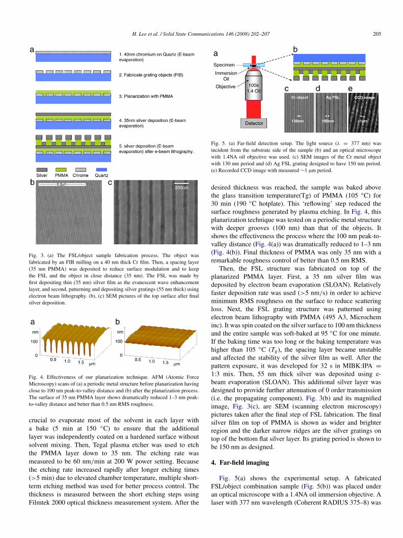
Fig. 5. (a) Far-field detection setup. The light source (λ = 377 nm) wasincident from the substrate side of the sample (b) and an optical microscopewith 1.4NA oil objective was used. (c) SEM images of the Cr metal objectwith 130 nm period and (d) Ag FSL grating designed to have 150 nm period.(e) Recorded CCD image with measured ∼1 µm period.
desired thickness was reached, the sample was baked abovethe glass transition temperature(Tg) of PMMA (105 ◦C) for30 min (190 ◦C hotplate). This ‘reflowing’ step reduced thesurface roughness generated by plasma etching. In Fig. 4, thisplanarization technique was tested on a periodic metal structurewith deeper grooves (100 nm) than that of the objects. Itshows the effectiveness the process where the 100 nm peak-to-valley distance (Fig. 4(a)) was dramatically reduced to 1–3 nm(Fig. 4(b)). Final thickness of PMMA was only 35 nm with aremarkable roughness control of better than 0.5 nm RMS.
Then, the FSL structure was fabricated on top of theplanarized PMMA layer. First, a 35 nm silver film wasdeposited by electron beam evaporation (SLOAN). Relativelyfaster deposition rate was used (>5 nm/s) in order to achieveminimum RMS roughness on the surface to reduce scatteringloss. Next, the FSL grating structure was patterned usingelectron beam lithography with PMMA (495 A3, Microcheminc). It was spin coated on the silver surface to 100 nm thicknessand the entire sample was soft-baked at 95 ◦C for one minute.If the baking time was too long or the baking temperature washigher than 105 ◦C (Tg), the spacing layer became unstableand affected the stability of the silver film as well. After thepattern exposure, it was developed for 32 s in MIBK:IPA =
1:3 mix. Then, 55 nm thick silver was deposited using e-beam evaporation (SLOAN). This additional silver layer wasdesigned to provide further attenuation of 0 order transmission(i.e. the propagating component). Fig. 3(b) and its magnifiedimage, Fig. 3(c), are SEM (scanning electron microscopy)pictures taken after the final step of FSL fabrication. The finalsilver film on top of PMMA is shown as wider and brighterregion and the darker narrow ridges are the silver gratings ontop of the bottom flat silver layer. Its grating period is shown tobe 150 nm as designed.
4. Far-field imaging
Fig. 5(a) shows the experimental setup. A fabricatedFSL/object combination sample (Fig. 5(b)) was placed underan optical microscope with a 1.4NA oil immersion objective. Alaser with 377 nm wavelength (Coherent RADIUS 375–8) was

206 H. Lee et al. / Solid State Communications 146 (2008) 202–207
Fig. 6. (a) Relative intensity cross-section of images recorded by CCD vs. various object periods. (b) Experimental (blue squares) and calculated (red curve) OTFsplotted against lateral wave vectors show good agreement. SEM image (c) and the FSL reconstructed image (d) of a testing three-line object. The line width is 50 nmand the centre distance is 120 nm between each line. The scale bar represents 200 nm in both (c) and (d). (For interpretation of the references to colour in this figurelegend, the reader is referred to the web version of this article.)
used to illuminate the sample and its transmission image wasmeasured by a UV sensitive CCD detector (Roper Scientific).
Fig. 5(c) and (d) are SEM images of a 130 nm period objectand a FSL grating. From the simple grating law, 1
Λdetected=
1Λobj
−1
ΛFSL, the period of a captured image (Λdetected) was
calculated to be 975 nm. The measured image period of1 µm (Fig. 5(e)) is consistent with the calculated value. Thisresult can be explained as a near field moire effect where asimple wave vector mixing of two periodic structures generatesanother periodic image [16]. However, the uniqueness of aFSL imaging comes from its ability to selectively enhancea certain evanescent band (i.e. spatial frequency dependentoptical-transfer function) necessary for the retrieval of theoriginal wave vector information [1]. The relative intensities ofthe real images captured by the CCD vs. the object periodicitiesare plotted in Fig. 6(a). In Fig. 6(b), the spatial frequencydependent transmission behaviour of the FSL is plotted againstthe wave vector of each grating object based on the data shownin Fig. 6(a). The experimental OTF (blue squares) is comparedwith the theoretical calculation (red curve), which shows closeagreement with each other even though the experimental OTFshows rather smooth but acceptably transitional cut-off inreference to the ideal sharp cut-off (vertical dotted line) at2.5k0. This selective enhancement behaviour is an essentialfunction of FSL generating one-to-one mapping between themeasured and the original information [1].
5. Image reconstruction
After the experimental verification of the OTF, an objectwith broader spectrum was fabricated and imaged with a FSL.Fig. 6(c) shows the SEM image of a three-line object withcentre-to-centre distances of 120 nm. Using the FSL, thescattered signal was captured in the far field and the originalobject image was numerically reconstructed (Fig. 6(d)) whichshowed the clearly resolved three-line object. It is possibleto resolve even smaller objects since the enhancement bandextends to 4k0, which represents feature sizes below 100 nm.
The image reconstruction can be done in real-time withoutusing numerical methods as we discussed in our previouswork [2], by combining information from both p (representing
Fig. 7. Schematic setup to realize real-time image reconstruction by optics.Two polarizations which carry different information of the object canbe separated by beam splitter 1 and modified individually. The finalmagnified subdiffraction-limited image can be obtained by recombining bothpolarizations.
evanescent information) and s polarization (representingpropagating information) in one optical setup shown in Fig. 7.As an object scatters nonpolarized incident light, the p-polarized evanescent portion (P1 and P2 bands in Fig. 1) isenhanced and scattered by the FSL grating. Considering themicroscope objective NA value of 1.4, the P1 and P2 bands(Fig. 1(b)) collected by this objective |k| < 1.4k0 originallycome from the evanescent band, 2.5k0 < |k| < 3.9k0. Inaddition, because the objective has 100 time magnification, thepropagating wave vectors are compressed by 100 times andbecome |k| < 0.014k0. Then, P1 and P2 can be shifted backto 0.025k0 < |k| < 0.039k0 by first order diffraction of agrating with the period of 100 times larger than the FSL grating.The 0 order diffraction of this grating can be filtered out at theFourier plane, between Lens 1 and Lens 2. The initial objectinformation 2.5k0 < |k| < 3.9k0 carried by the p-polarizationare finally converted into band 0.025k0 < |k| < 0.039k0.

H. Lee et al. / Solid State Communications 146 (2008) 202–207 207
Since there is no field enhancement involved for s-polarization,all of the evanescent information is negligible. Therefore, thepropagating waves with |k| < 1.4k0 are converted into the band|k| < 0.014k0 just as a conventional microscope does and afilter or a screen can be placed at the Fourier plane betweenLens 3 and Lens 4 to selectively control the contribution of thes polarization to the final image. The p and s information arethen combined at the CCD image plane to give a subdiffraction-limited image of the object.
6. Conclusion
A promising nanoscale imaging method called FSL imagingwas developed and experimentally demonstrated. A FSLnot only enhances but also projects evanescent wave to farfield, enabling a subdiffraction-limited imaging. The detailedfabrication process and the optical characterization werepresented and discussed. Object with 70 nm gap distanceand 120nm centre-to-centre distance was resolved in the farfield. A novel FSL optics setup was proposed which enablesreal-time nanoscale imaging in the far field without the useof any numerical reconstruction algorithm. The FSL conceptpresented in this report is not limited to 1D imaging only.We have also developed a FSL capable of true 2D imagingwhich will be published elsewhere. The FSL opens thedoor to overcome the diffraction limit [2] and has potentialapplications in high resolution real-time bio-imaging andnanoscale lithography also with the possibility to work invarious wavelengths [17].
Acknowledgements
This research is supported by the Center for Scalable andIntegrated Nanomanufacturing (SINAM), and NSF NanoscaleScience and Engineering Center (NSEC) under award no.DMI-0327077, and Army Research Office MURI program(grant no. 50432-PHMUR).
References
[1] S. Durant, J. Opt. Soc. Am. B. 23 (2006) 2383.[2] Z. Liu, S. Durant, H. Lee, Y. Pikus, N. Fang, Y. Xiong, C. Sun, X. Zhang,
Nano Lett. 7 (2007) 403.[3] E. Abbe, Arch. Mikroskop. Anat. 9 (1873) 413.[4] E. Betzig, J.K. Trautman, T.D. Harris, J.S. Weiner, R.K. Kostelak, Science
251 (1991) 1468.[5] S.W. Hell, Nat. Biotechnol. 21 (2003) 1347.[6] Z. Liu, H. Lee, Y. Xiong, C. Sun, X. Zhang, Science 315 (2007) 1686.[7] J.B. Pendry, Phys. Rev. Lett. 85 (2000) 3966.[8] N. Fang, H. Lee, C. Sun, X. Zhang, Science 308 (2005) 534–537.[9] H. Lee, Y. Xiong, N. Fang, W. Srituravanich, S. Durant, M. Ambati, C.
Sun, X. Zhang, New J. Phys. 7 (2005) 255.[10] D.O.S. Melville, R.J. Blaikie, Opt. Express. 13 (2005) 2127.[11] T. Taubner, D. Korobkin, Y. Urzhumov, G. Shvets, R. Hillenbrand,
Science 313 (2006) 1595.[12] V. Podolskiy, E.E. Narimanov, Opt. Lett. 30 (2005) 75.[13] M.G.L. Gustafsson, J. Microsc. 198 (2000) 82.[14] Z. Liu, N. Fang, T.J. Yen, X. Zhang, Appl. Phys. Lett. 83 (2003) 5184.[15] L.E. Stillwagon, R.G. Larson, Phys. Fluids A 2 (1990) 1937.[16] Z. Liu, S. Durant, H. Lee, Y. Xiong, Y. Pikus, C. Sun, X. Zhang, Opt. Lett.
32 (2007) 629.[17] Y. Xiong, Z. Liu, S. Durant, H. Lee, C. Sun, X. Zhang, Opt. Express 15
(2007) 7095.


![����-��Q�kTitle ����-��Q�k Author ï¿½ï¿½ï¿½Ý t�]�c Created Date �����-�](https://static.fdocuments.us/doc/165x107/60a3a35fc4ece70e851f9842/-qk-title-qk.jpg)


![29 Pieces - Collection of easy pieces [(1st and 2nd grade)] · PDF file3 4 Ï Ï Ï Ï Ï Ï Ï Ï Ï Ï Ï Ï Ï Ï Ï Ï Ï Ï Ï Ï Ï Ï Ï Ï Ï hh. . h. hh. . 3. 3 f 4 4 2 1](https://static.fdocuments.us/doc/165x107/5a74e1047f8b9ad22a8c2b1a/29-pieces-collection-of-easy-pieces-1st-and-2nd-grade-a-3-4-a-a.jpg)
