
DESIGN EXAMPLE REPORT - Power Integrations · DESIGN EXAMPLE REPORT Title 35 W Power Supply Using...
32
Power Integrations 5245 Hellyer Avenue, San Jose, CA 95138 USA. Tel: +1 408 414 9200 Fax: +1 408 414 9201 www.powerint.com DESIGN EXAMPLE REPORT Title 35 W Power Supply Using TOP257EN Specification 90 VAC – 264 VAC Input; 13 V, 2.69 A Output Application LCD Monitor Author Applications Engineering Department Document Number DER-187 Date June 24, 2008 Revision 1.0 Summary and Features • Low cost, low component count, high efficiency • Delivers 35 W in a 50 °C ambient temperature environment • EcoSmart ® – meets requirements for low no-load and standby power consumption • 0.55 W output power for <1 W input power • No-load power consumption: <200 mW at 230 VAC • >82% Full-load efficiency • Integrated safety and reliability features • Accurate, auto-recovering, hysteretic thermal shutdown function maintains safe PCB temperatures under all conditions • Auto-restart protects against output short circuits and feedback open- loop failures • Output overvoltage protection (OVP) configurable for latching or self-recovery • Input under-voltage (UV) protection prevents power up or power-down output glitches • Easily meets EN55022 and CISPR-22 Class B conducted EMI: >6 dB margin PATENT INFORMATION The products and applications illustrated herein (including transformer construction and circuits external to the products) may be covered by one or more U.S. and foreign patents, or potentially by pending U.S. and foreign patent applications assigned to Power Integrations. A complete list of Power Integrations' patents may be found at www.powerint.com. Power Integrations grants its customers a license under certain patent rights as set forth at <http://www.powerint.com/ip.htm>.
Transcript of DESIGN EXAMPLE REPORT - Power Integrations · DESIGN EXAMPLE REPORT Title 35 W Power Supply Using...

Power Integrations
5245 Hellyer Avenue, San Jose, CA 95138 USA. Tel: +1 408 414 9200 Fax: +1 408 414 9201
www.powerint.com
DESIGN EXAMPLE REPORT
Title 35 W Power Supply Using TOP257EN
Specification 90 VAC – 264 VAC Input; 13 V, 2.69 A Output
Application LCD Monitor
Author Applications Engineering Department
Document Number
DER-187
Date June 24, 2008
Revision 1.0
Summary and Features
• Low cost, low component count, high efficiency
• Delivers 35 W in a 50 °C ambient temperature environment
• EcoSmart® – meets requirements for low no-load and standby power consumption
• 0.55 W output power for <1 W input power
• No-load power consumption: <200 mW at 230 VAC
• >82% Full-load efficiency
• Integrated safety and reliability features
• Accurate, auto-recovering, hysteretic thermal shutdown function maintains safe PCB temperatures under all conditions
• Auto-restart protects against output short circuits and feedback open- loop failures
• Output overvoltage protection (OVP) configurable for latching or self-recovery
• Input under-voltage (UV) protection prevents power up or power-down output glitches
• Easily meets EN55022 and CISPR-22 Class B conducted EMI: >6 dB margin
PATENT INFORMATION
The products and applications illustrated herein (including transformer construction and circuits external to the products) may be covered
by one or more U.S. and foreign patents, or potentially by pending U.S. and foreign patent applications assigned to Power Integrations. A
complete list of Power Integrations' patents may be found at www.powerint.com. Power Integrations grants its customers a license under
certain patent rights as set forth at <http://www.powerint.com/ip.htm>.

DER-187 – 35 W LCD Monitor, TOP257EN 13 V Output Supply 24-Jun-08
Page 2 of 32
Power Integrations Tel: +1 408 414 9200 Fax: +1 408 414 9201 www.powerint.com
Table of Contents 1 Introduction.................................................................................................................3
2 Power Supply Specification ........................................................................................4
3 Schematic...................................................................................................................5
4 Circuit Description ......................................................................................................6
4.1 Input EMI Filtering ...............................................................................................6
4.2 TOPSwitch HX Primary .......................................................................................6
4.3 Output Rectification .............................................................................................7
4.4 Output Feedback.................................................................................................8
5 PCB Layout ................................................................................................................9
6 Bill of Materials .........................................................................................................10
7 Inductor (L1) Electrical and Build Diagram ...............................................................12
8 Transformer Specification.........................................................................................13
8.1 Electrical Diagram .............................................................................................13
8.2 Electrical Specifications.....................................................................................13
8.3 Materials............................................................................................................13
8.4 Transformer Build Diagram ...............................................................................14
8.5 Transformer Construction..................................................................................14
9 Transformer Spreadsheets.......................................................................................15
10 Performance Data.................................................................................................18
10.1 Efficiency...........................................................................................................18
10.2 No-load Input Power..........................................................................................19
10.3 Available Standby Output Power.......................................................................19
10.4 Regulation .........................................................................................................20
10.4.1 Load ...........................................................................................................20
10.4.2 Line ............................................................................................................20
11 Thermal Performance ...........................................................................................21
12 Waveforms............................................................................................................22
12.1 Drain Voltage and Current, Normal Operation...................................................22
12.2 Output Voltage Start-up Profile..........................................................................22
12.3 Drain Voltage and Current Start-up Profile ........................................................23
12.4 Load Transient Response (50% to 100% Load Step) .......................................23
12.5 Open-loop Protection ........................................................................................24
12.6 Output Ripple Measurements............................................................................25
12.6.1 Ripple Measurement Technique ................................................................25
12.6.2 Measurement Results ................................................................................26
13 Control Loop Measurements.................................................................................27
14 Line Surge.............................................................................................................29
15 Conducted EMI .....................................................................................................30
16 Revision History ....................................................................................................31
Important Note: Although this board is designed to satisfy safety isolation requirements, the engineering prototype has not been agency approved. Therefore, all testing should be performed using an isolation transformer to provide the AC input to the prototype board.

24-Jun-08 DER-187 – 35 W LCD Monitor, TOP257EN 13 V Output Supply
Page 3 of 32
Power Integrations Tel: +1 408 414 9200 Fax: +1 408 414 9201
www.powerint.com
1 Introduction
This engineering report describes an LCD monitor power supply utilizing the TOPSwitch®-HX TOP257EN in a universal input, single output (13 V, 2.69 A) flyback-converter configuration. This document contains specifications for the power supply and transformer, the design schematic, bill of materials, printed circuit board layout, and power supply performance specifications.
Figure 1 – Populated Circuit Board Photograph.

DER-187 – 35 W LCD Monitor, TOP257EN 13 V Output Supply 24-Jun-08
Page 4 of 32
Power Integrations Tel: +1 408 414 9200 Fax: +1 408 414 9201 www.powerint.com
2 Power Supply Specification
Description Symbol Min Typ Max Units Comment
Input
Voltage VIN 90 264 VAC
Frequency fLINE 47 50/60 64 Hz
No-load Input Power (265 VAC) 0.18 0.3 W
Output
Output Voltage 1 VOUT1 13 V ± 5%
Output Ripple Voltage 1 VRIPPLE1 100 mV 20 MHz bandwidth
Output Current 1 IOUT1 2.69 A
Total Output Power
Continuous Output Power POUT 35 W
Efficiency
Full Load η 82 % Vin 90 VAC measured
at POUT 25 o
C
Average active efficiency 25%, 50%, 75%, 100 % of POUT
ηCEC 82 84 % Per California Energy Commission (CEC) / Energy Star requirements
Environmental
Conducted EMI Meets CISPR22B / EN55022B
Safety Designed to meet IEC950, UL1950
Class II
Surge Differential Common Mode
1 2
kV kV
1.2/50 µs surge, IEC 1000-4-5, series impedance:
differential mode: 2 Ω
common mode: 12 Ω
Surge Ring Wave
1 kV 100 kHz ring wave, 500 A short-circuit current; differential and
common modes
Ambient Temperature TAMB 0 50 oC Free convection, sea level

24-Jun-08 DER-187 – 35 W LCD Monitor, TOP257EN 13 V Output Supply
Page 5 of 32
Power Integrations Tel: +1 408 414 9200 Fax: +1 408 414 9201
www.powerint.com
3 Schematic
Figure 2 – Schematic.
DER-187 – 35 W LCD Monitor, TOP257EN 13 V Output Supply 24-Jun-08
Page 6 of 32
Power Integrations Tel: +1 408 414 9200 Fax: +1 408 414 9201 www.powerint.com
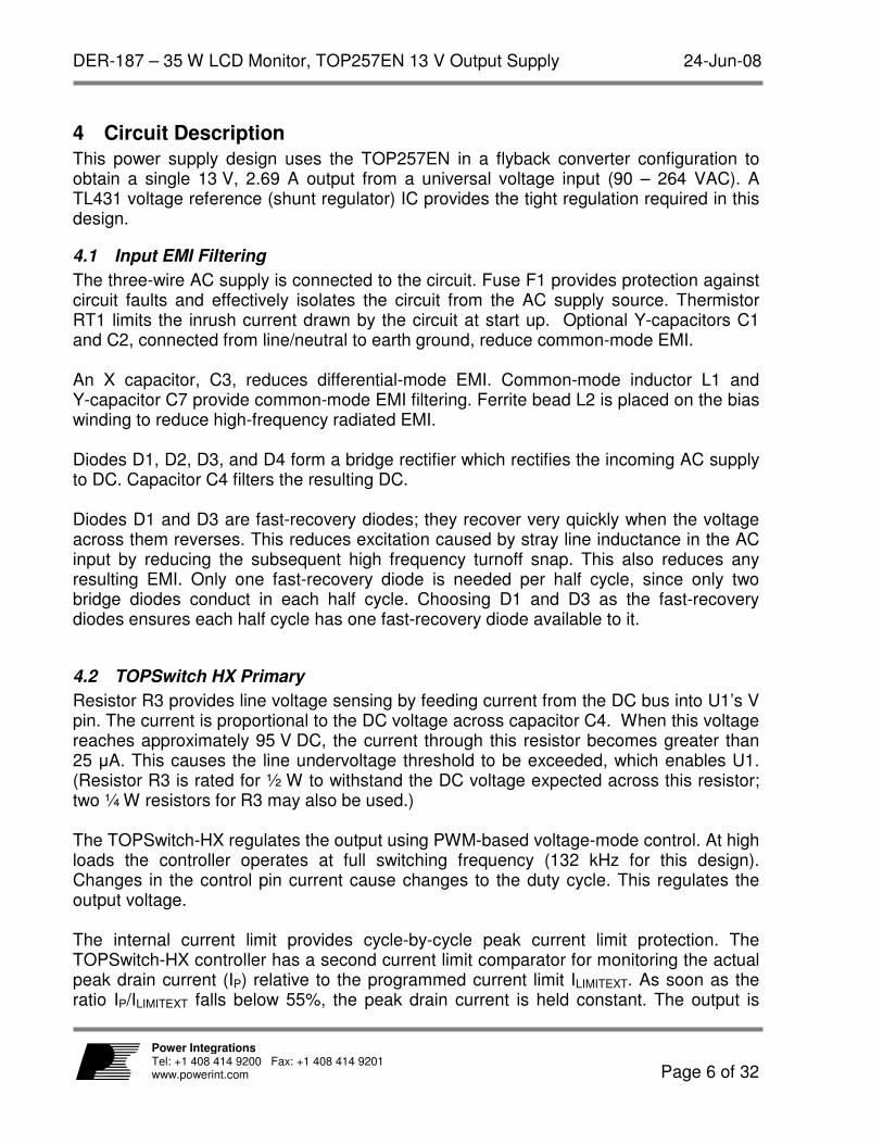
4 Circuit Description
This power supply design uses the TOP257EN in a flyback converter configuration to obtain a single 13 V, 2.69 A output from a universal voltage input (90 – 264 VAC). A TL431 voltage reference (shunt regulator) IC provides the tight regulation required in this design.
4.1 Input EMI Filtering
The three-wire AC supply is connected to the circuit. Fuse F1 provides protection against circuit faults and effectively isolates the circuit from the AC supply source. Thermistor RT1 limits the inrush current drawn by the circuit at start up. Optional Y-capacitors C1 and C2, connected from line/neutral to earth ground, reduce common-mode EMI. An X capacitor, C3, reduces differential-mode EMI. Common-mode inductor L1 and Y-capacitor C7 provide common-mode EMI filtering. Ferrite bead L2 is placed on the bias winding to reduce high-frequency radiated EMI. Diodes D1, D2, D3, and D4 form a bridge rectifier which rectifies the incoming AC supply to DC. Capacitor C4 filters the resulting DC. Diodes D1 and D3 are fast-recovery diodes; they recover very quickly when the voltage across them reverses. This reduces excitation caused by stray line inductance in the AC input by reducing the subsequent high frequency turnoff snap. This also reduces any resulting EMI. Only one fast-recovery diode is needed per half cycle, since only two bridge diodes conduct in each half cycle. Choosing D1 and D3 as the fast-recovery diodes ensures each half cycle has one fast-recovery diode available to it.
4.2 TOPSwitch HX Primary
Resistor R3 provides line voltage sensing by feeding current from the DC bus into U1’s V pin. The current is proportional to the DC voltage across capacitor C4. When this voltage reaches approximately 95 V DC, the current through this resistor becomes greater than 25 µA. This causes the line undervoltage threshold to be exceeded, which enables U1. (Resistor R3 is rated for ½ W to withstand the DC voltage expected across this resistor; two ¼ W resistors for R3 may also be used.) The TOPSwitch-HX regulates the output using PWM-based voltage-mode control. At high loads the controller operates at full switching frequency (132 kHz for this design). Changes in the control pin current cause changes to the duty cycle. This regulates the output voltage. The internal current limit provides cycle-by-cycle peak current limit protection. The TOPSwitch-HX controller has a second current limit comparator for monitoring the actual peak drain current (IP) relative to the programmed current limit ILIMITEXT. As soon as the ratio IP/ILIMITEXT falls below 55%, the peak drain current is held constant. The output is

24-Jun-08 DER-187 – 35 W LCD Monitor, TOP257EN 13 V Output Supply
Page 7 of 32
Power Integrations Tel: +1 408 414 9200 Fax: +1 408 414 9201
www.powerint.com
then regulated by modulating the switching frequency. (This is the variable frequency PWM control mode.) As the load continues to decrease, the switching frequency also decreases linearly down to 30 kHz. Once the switching frequency drops to 30 kHz, the controller keeps it constant and reduces the peak current to regulate the output. (This is the fixed frequency, direct duty cycle PWM control mode.) As the load continues to decrease and the ratio IP/ILIMITEXT falls below 25%, the controller enters multi-cycle-modulation mode. This mode offers excellent efficiency under light-load conditions (such as in standby operation), and low no-load input power consumption. Diode D5 forms a clamp network with C6, R1, and R2 that limits the drain voltage of U1 at the instant of turn-off. Using a fast-recovery (rather than an ultra-fast) diode for D5, allows some of the clamp energy to be recovered. Resistor R1 limits reverse diode current and dampens high frequency ringing. The output of the bias winding is rectified by diode D6 and filtered by the combination of resistor R6 and capacitor C10. Capacitor C5 and resistor R4 dampen any high-frequency ringing caused by D6. This rectified and filtered output is used by optocoupler U2B to provide the control and supply current to the CONTROL terminal (C pin) of U1. Failure in the feedback circuit (caused by an open-loop condition) may cause the power supply output to exceed the regulation limit. The increased output voltage causes the voltage at the bias winding output to also increase. Under these conditions Zener diode VR2 breaks down and current flows into U1’s V pin, causing a latch-OVP shutdown. The power supply’s output voltage is regulated by the feedback circuit on the secondary side, which controls the output voltage by changing the optocoupler current. A change in the optocoupler current causes a change in current flowing into the C pin of U1. Variation of the current into the C pin results in a variation of the duty cycle, which regulates the power supply’s output voltage.
4.3 Output Rectification
Diodes D7 and D8 provide output rectification. Low-ESR capacitors C13 and C14 provide filtering. Inductor L3 and capacitor C15 form a second stage filter that significantly attenuates the switching noise across C13 and C14, ensuring a low noise output. The snubber network comprised of R10 and C12 dampens high-frequency ringing across diodes D7 and D8. The ringing results from transformer winding leakage inductance and secondary trace inductances.

DER-187 – 35 W LCD Monitor, TOP257EN 13 V Output Supply 24-Jun-08
Page 8 of 32
Power Integrations Tel: +1 408 414 9200 Fax: +1 408 414 9201 www.powerint.com
4.4 Output Feedback
The output voltage is controlled using shunt regulator U3. Resistors R13 and R14 form a voltage-divider network that senses the output, keeping the voltage in regulation. Resistor R12 and capacitor C16 are compensation elements around error amplifier U3 which set the feedback circuit frequency response. Resistor R11 sets the overall DC loop gain and limits the current through U2A during transient state conditions.

24-Jun-08 DER-187 – 35 W LCD Monitor, TOP257EN 13 V Output Supply
Page 9 of 32
Power Integrations Tel: +1 408 414 9200 Fax: +1 408 414 9201
www.powerint.com
5 PCB Layout
Figure 3 – Printed Circuit Layout.

DER-187 – 35 W LCD Monitor, TOP257EN 13 V Output Supply 24-Jun-08
Page 10 of 32
Power Integrations Tel: +1 408 414 9200 Fax: +1 408 414 9201 www.powerint.com
6 Bill of Materials Item Qty Ref Des Description Mfg Mfg Part Number
1 2 C1 C2 220 pF, Ceramic Y1 Vishay 440LT33-R
2 1 C3 100 nF, 275VAC, Film, X2 Vishay/Roederstein F1772-410-2000
3 1 C4 100 µF, 400 V, Electrolytic, Low ESR, 630 mΩ, (16 x 40)
Nippon Chemi-Con EKMX401ELL101ML40S
4 1 C5 1 nF, 100 V, Ceramic, X7R Epcos B37981M1102K000
5 1 C6 2.2 nF, 1 kV, Disc Ceramic NIC Components
Corp NCD222K1KVY5FF
6 1 C7 2.2 nF, Ceramic, Y1 Vishay 440LD22-R
7 1 C8 100 nF, 50 V, Ceramic, Z5U, .2Lead Space Kemet C317C104M5U5TA
8 1 C9 47 µF, 16 V, Electrolytic, Gen Purpose, (5 x 11.5)
Panasonic ECA-1CHG470
9 1 C10 22 µF, 50 V, Electrolytic, Very Low ESR, 340 mΩ, (5 x 11)
Nippon Chemi-Con EKZE500ELL220ME11D
10 1 C11 22 pF, 1 kV, Disc Ceramic Panasonic ECC-D3A220JGE
11 1 C12 470 pF, 100 V, Ceramic, COG AVX Corp 5NK471KOBAM
12 2 C13 C14 680 µF, 25 V, Electrolytic, Very Low ESR, 23 mΩ, (10 x 20)
Nippon Chemi-Con EKZE250ELL681MJ20S
13 1 C15 330 µF, 25 V, Electrolytic, Very Low ESR, 56 mΩ, (8 x 15)
Nippon Chemi-Con EKZE250ELL331MH15D
14 1 C16 47 nF, 50 V, Ceramic, Z5U Epcos B37982N5473M000
15 2 D1 D3 600 V, 1 A, Fast Recovery Diode, 200 ns, DO-41
On Semiconductor 1N4937RLG
16 2 D2 D4 1000 V, 1 A, Rectifier, DO-41 Vishay 1N4007-E3/54
17 1 D5 800 V, 1 A, Fast Recovery Diode, 500 ns, DO-41
Diodes Inc. FR106
18 1 D6 200 V, 200 mA, Fast Switching, 50 ns, DO-35 Vishay BAV20
19 2 D7 D8 80 V, 5 A, Schottky, DO-201AD Vishay SB580
20 1 F1 3.15 A, 250V,Fast, TR5 Wickman 37013150410
21 1 J1 5 Position (1 x 5) header, 0.156 pitch, Vertical Molex 26-48-1055
22 1 J3 2 Position (1 x 2) header, 0.156 pitch, Vertical, Straight-Friction Lock Header
Molex 26-48-1025
23 1 L1 9 mH, Common Mode Choke Custom
24 1 L2 3.5 mm x 7.6 mm, 75 Ohms at 25 MHz, 22 AWG hole, Ferrite Bead
Fair-Rite 2743004112
25 1 L3 3.3 µH, 5.5 A JW Miller RL622-3R3K-RC
26 2 R1 R10 33 Ω, 5%, 1/4 W, Carbon Film Yageo CFR-25JB-33R
27 1 R2 100 kΩ, 5%, 1/2 W, Carbon Film Yageo CFR-50JB-100K
28 1 R3 3.9 MΩ, 5%, 1/2 W, Carbon Film Yageo CFR-50JB-3M9
29 1 R4 33 Ω, 5%, 1/8 W, Carbon Film Yageo CFR-12JB-33R
30 1 R5 20 Ω, 5%, 1/4 W, Carbon Film Yageo CFR-25JB-20R
31 1 R6 4.7 Ω, 5%, 1/4 W, Carbon Film Yageo CFR-25JB-4R7
32 1 R7 15.4 kΩ, 1%, 1/4 W, Metal Film Yageo MFR-25FBF-15K4
33 1 R8 10 Ω, 5%, 1/8 W, Carbon Film Yageo CFR-12JB-10R
34 1 R9 100 Ω, 5%, 1/4 W, Carbon Film Yageo CFR-25JB-100R
35 1 R11 1.2 kΩ, 5%, 1/4 W, Carbon Film Yageo CFR-25JB-1K2
36 1 R12 10 kΩ 5%, 1/4 W, Carbon Film Yageo CFR-25JB-10K

24-Jun-08 DER-187 – 35 W LCD Monitor, TOP257EN 13 V Output Supply
Page 11 of 32
Power Integrations Tel: +1 408 414 9200 Fax: +1 408 414 9201
www.powerint.com
37 1 R13 42.2 kΩ 1%, 1/4 W, Metal Film Yageo MFR-25FBF-42K2
38 1 R14 10 kΩ, 1%, 1/4 W, Metal Film Panasonic ERO-S2PHF1002
39 1 RT1 NTC Thermistor, 10 Ώ, 1.7 A Thermometrics CL-120
40 1 T1 Bobbin, EF25,(E25/13/7) Horizontal, 10 pins Epcos B66208-A1110-T1
41 1 U1 TOPSwitch-HX, TOP257EN, eSIP-7C Power Integrations TOP257EN
42 1 U2 Optocoupler, 35 V, CTR 80-160%, 4-DIP Liteon LTV-817A
43 1 U3 2.495 V Shunt Regulator IC, 2%, 0 to 70C, TO-92
On Semiconductor TL431CLPG
44 1 VR2 28 V, 5%, 500 mW, DO-35 Diodes Inc 1N5255B-T

DER-187 – 35 W LCD Monitor, TOP257EN 13 V Output Supply 24-Jun-08
Page 12 of 32
Power Integrations Tel: +1 408 414 9200 Fax: +1 408 414 9201 www.powerint.com
7 Inductor (L1) Electrical and Build Diagram
Figure 4 – L1 Common-mode Inductor Specifications.

24-Jun-08 DER-187 – 35 W LCD Monitor, TOP257EN 13 V Output Supply
Page 13 of 32
Power Integrations Tel: +1 408 414 9200 Fax: +1 408 414 9201
www.powerint.com
8 Transformer Specification
8.1 Electrical Diagram
Figure 5 – Transformer Electrical Diagram.
8.2 Electrical Specifications
Electrical Strength 1 second, 60 Hz, from Pins 1-5 to Pins 6-10 3000 VAC
Primary Inductance Pins 1-2, all other windings open, measured at 100 kHz.
690 µH, ± 5%
Resonant Frequency Pins 1-2, all other windings open 1.8 MHz (Min.)
Primary Leakage Inductance Pins 1-2, with Pins 4-10 shorted, measured at
100 kHz. 13 µH (Max.)
8.3 Materials
Item Description
[1] Core: EF25 Gapped For ALG=220 nH/T^2
[2] Bobbin: EF25 10 Pins Horizontal. See Note Below
[3] Magnet Wire #26 AWG
[4] Magnet Wire #30 AWG
[5] Magnet Wire #39 AWG
[6] Triple Insulated Wire: #23 AWG
[7] Margin Tape 2 mm wide
[8] Tape, 3M1350F-1 13.6 mm Wide
[9] Tape, 3M1350F-1 15.6 mm Wide
[10] Varnish
NOTE: The bobbin used on this transformer design does not meet safety requirements. To meet safety regulations using this design, replace it with bobbin YC-2504 from Ying Chin Co Ltd.

DER-187 – 35 W LCD Monitor, TOP257EN 13 V Output Supply 24-Jun-08
Page 14 of 32
Power Integrations Tel: +1 408 414 9200 Fax: +1 408 414 9201 www.powerint.com
8.4 Transformer Build Diagram
Figure 6 – Transformer Build Diagram.
8.5 Transformer Construction
Bobbin Preparation Place bobbin (item [2]) on the winding machine with the primary-pins side oriented to the left-hand side.
Primary Margin Apply 2 mm wide margin of tape (item [7]) on secondary side. Match height of primary and bias windings.
WD1 First Half Primary
Start at Pin 2. Wind 29 turns of item [3] from left to right in 1 layer. Finish on Pin 3.
Basic Insulation Use two layers of item [8] for basic insulation.
WD2 Bias Winding Starting at Pin 5, wind 8 quad-filar turns of item [4]. Wind from left to right and spread turns evenly across bobbin. Finish at Pin 4.
Basic Insulation Use one layer of item [9] for basic insulation.
WD3 Secondary Winding
Start temporarily on pins 3 and 4. Wind 7 bi-filar turns of item [6] in 1 layer. Wind from left to right and finish on pins 7 and 8. Bend the starting leads toward the secondary side and connect them, respectively, to pins 9 and 10.
Basic Insulation Use one layer of item [9] for basic insulation.
Primary Margin Apply 2 mm wide margin of Item [7] on secondary side. Match height of shield and primary windings.
WD4 Shield Start Temporarily on pin 3, wind from left to right 9 quad-filar turns of item [5]. Finish on Pin 1. Cut the starting terminal at the beginning of the winding.
Basic Insulation Use one layer of item [8] for basic insulation.
WD5 Second Half Primary.
Start at Pin 3. Wind 27 turns of item [3] from left to right in 1 layer. Finish on Pin 1.
Outer Wrap Wrap windings with 3 layers of tape (item [9]).
Final Assembly Assemble and secure core halves. Varnish impregnate (item [10]).

24-Jun-08 DER-187 – 35 W LCD Monitor, TOP257EN 13 V Output Supply
Page 15 of 32
Power Integrations Tel: +1 408 414 9200 Fax: +1 408 414 9201
www.powerint.com
9 Transformer Spreadsheets
ACDC_TOPSwitchHX_021308; Rev.1.8; Copyright Power Integrations 2008
INPUT INFO OUTPUT UNIT
TOP_HX_021308: TOPSwitch-HX Continuous/Discontinuous Flyback Transformer Design Spreadsheet
ENTER APPLICATION VARIABLES Customer
VACMIN 90 Volts Minimum AC Input Voltage
VACMAX 264 Volts Maximum AC Input Voltage
fL 50 Hertz AC Mains Frequency
VO 13.00 Volts Output Voltage (main)
PO_AVG 35.00 Watts Average Output Power
PO_PEAK 35.00 Watts Peak Output Power
n 0.83 %/100 Efficiency Estimate
Z 0.50 Loss Allocation Factor
VB 15 Volts Bias Voltage
tC 3.00 mSeconds Bridge Rectifier Conduction Time Estimate
CIN 100.0 100 uFarads Input Filter Capacitor
ENTER TOPSWITCH-HX VARIABLES
TOPSwitch-HX TOP257EN Universal /
Peak 115 Doubled/230 V
Chosen Device TOP257EN Power
Out 119 W / 119
W 157 W
KI 0.37 External ILIMIT reduction factor (KI=1.0 for default ILIMIT, KI <1.0 for lower ILIMIT)
ILIMITMIN_EXT 1.170 Amps Use 1% resistor in setting external ILIMIT
ILIMITMAX_EXT 1.346 Amps Use 1% resistor in setting external ILIMIT Frequency (F)=132kHz, (H)=66kHz F F
Select 'H' for Half frequency – 66 kHz, or 'F' for Full frequency – 132 kHz
fS 132000 Hertz TOPSwitch-HX Switching Frequency: Choose between 132 kHz and 66 kHz
fSmin 119000 Hertz TOPSwitch-HX Minimum Switching Frequency
fSmax 145000 Hertz TOPSwitch-HX Maximum Switching Frequency High Line Operating Mode FF Full Frequency, Jitter enabled
VOR 108.00 Volts Reflected Output Voltage
VDS 10 Volts TOPSwitch on-state Drain-to-source Voltage
VD 0.50 Volts Output Winding Diode Forward-voltage Drop
VDB 0.70 Volts Bias Winding Diode Forward-voltage Drop
KP 0.59 Ripple to Peak Current Ratio (0.3 < KRP < 1.0 : 1.0< KDP<6.0)
PROTECTION FEATURES
LINE SENSING
VUV_STARTUP 95 95 Volts Minimum DC Bus Voltage at which the power supply will start-up
VOV_SHUTDOWN 490 Volts Typical DC Bus Voltage at which power supply will shut-down (Max)
RLS 4 M-ohms Use two standard, 2.2 M-Ohm, 5% resistors in series for line sense functionality.
OUTPUT OVERVOLTAGE

DER-187 – 35 W LCD Monitor, TOP257EN 13 V Output Supply 24-Jun-08
Page 16 of 32
Power Integrations Tel: +1 408 414 9200 Fax: +1 408 414 9201 www.powerint.com
VZ 27 Volts Zener Diode rated voltage for Output Overvoltage shutdown protection
RZ 5.1 k-ohms Output OVP resistor. For latching shutdown use 20 ohm resistor instead
OVERLOAD POWER LIMITING
Overload Current Ratio at VMAX 1.2
Enter the desired margin to current limit at VMAX. A value of 1.2 indicates that the current limit should be 20% higher than peak primary current at VMAX
Overload Current Ratio at VMIN 1.06 Margin to current limit at low line.
ILIMIT_EXT_VMIN 1.09 A Peak primary Current at VMIN
ILIMIT_EXT_VMAX 1.04 A Peak Primary Current at VMAX
RIL 15.49 k-ohms Current limit/Power Limiting resistor.
RPL N/A M-ohms Resistor not required. Use RIL resistor only
Core Type EF25 EF25 Core Type
Core EF25 P/N: PC40EF25-Z
Bobbin EF25_BOB
BIN P/N: *
AE 0.518 cm^2 Core Effective Cross Sectional Area
LE 5.78 cm Core Effective Path Length
AL 2000 nH/T^2 Ungapped Core Effective Inductance
BW 15.6 mm Bobbin Physical Winding Width
M 1.00 mm Safety Margin Width (Half the Primary to Secondary Creepage Distance)
L 2.00 Number of Primary Layers
NS 7 7 Number of Secondary Turns
DC INPUT VOLTAGE PARAMETERS
VMIN 101 Volts Minimum DC Input Voltage
VMAX 373 Volts Maximum DC Input Voltage
CURRENT WAVEFORM SHAPE PARAMETERS
DMAX 0.54 Maximum Duty Cycle (calculated at PO_PEAK)
IAVG 0.42 Amps Average Primary Current (calculated at average output power)
IP 1.09 Amps Peak Primary Current (calculated at Peak output power)
IR 0.64 Amps Primary Ripple Current (calculated at average output power)
IRMS 0.58 Amps Primary RMS Current (calculated at average output power)
TRANSFORMER PRIMARY DESIGN PARAMETERS
LP 690 uHenries Primary Inductance
LP Tolerance 5 5 Tolerance of Primary Inductance
NP 56 Primary Winding Number of Turns
NB 8 Bias Winding Number of Turns
ALG 220 nH/T^2 Gapped Core Effective Inductance
BM 2590 Gauss Maximum Flux Density at PO, VMIN (BM<3000)

24-Jun-08 DER-187 – 35 W LCD Monitor, TOP257EN 13 V Output Supply
Page 17 of 32
Power Integrations Tel: +1 408 414 9200 Fax: +1 408 414 9201
www.powerint.com
BP 3362 Gauss
Peak Flux Density (BP<4200) at ILIMITMAX and LP_MAX. Note: Recommended values for adapters and external power supplies <=3600 Gauss
BAC 765 Gauss AC Flux Density for Core Loss Curves (0.5 X Peak to Peak)
ur 1776 Relative Permeability of Ungapped Core
LG 0.26 mm Gap Length (Lg > 0.1 mm)
BWE 27.2 mm Effective Bobbin Width
OD 0.49 mm Maximum Primary Wire Diameter including insulation
INS 0.06 mm Estimated Total Insulation Thickness (= 2 * film thickness)
DIA 0.42 mm Bare conductor diameter
AWG 26 AWG Primary Wire Gauge (Rounded to next smaller standard AWG value)
CM 256 Cmils Bare conductor effective area in circular mils
CMA 441 Cmils/Amp Primary Winding Current Capacity (200 < CMA < 500)
Primary Current Density (J) 4.54
Amps/mm^2
Primary Winding Current density (3.8 < J < 9.75)
Lumped parameters
ISP 8.71 Amps Peak Secondary Current
ISRMS 4.28 Amps Secondary RMS Current
IO_PEAK 2.69 Amps Secondary Peak Output Current
IO 2.69 Amps Average Power Supply Output Current
IRIPPLE 3.32 Amps Output Capacitor RMS Ripple Current
CMS 856 Cmils Secondary Bare Conductor minimum circular mils
AWGS 20 AWG Secondary Wire Gauge (Rounded up to next larger standard AWG value)
DIAS 0.81 mm Secondary Minimum Bare Conductor Diameter
ODS 1.94 mm Secondary Maximum Outside Diameter for Triple Insulated Wire
INSS 0.56 mm Maximum Secondary Insulation Wall Thickness
VOLTAGE STRESS PARAMETERS
VDRAIN 588 Volts Maximum Drain Voltage Estimate (Includes Effect of Leakage Inductance)
PIVS 60 Volts Output Rectifier Maximum Peak Inverse Voltage
PIVB 69 Volts Bias Rectifier Maximum Peak Inverse Voltage

DER-187 – 35 W LCD Monitor, TOP257EN 13 V Output Supply 24-Jun-08
Page 18 of 32
Power Integrations Tel: +1 408 414 9200 Fax: +1 408 414 9201 www.powerint.com
10 Performance Data
All measurements performed at room temperature.
10.1 Efficiency
50
60
70
80
90
100
90 110 130 150 170 190 210 230 250 270
Line Voltage (AC)
Ou
tpu
t E
ffic
ien
cy
(%
)
Figure 7 – Efficiency vs. Input Voltage, Room Temperature.

24-Jun-08 DER-187 – 35 W LCD Monitor, TOP257EN 13 V Output Supply
Page 19 of 32
Power Integrations Tel: +1 408 414 9200 Fax: +1 408 414 9201
www.powerint.com
10.2 No-load Input Power
100
120
140
160
180
200
220
90 110 130 150 170 190 210 230 250 270
Input Voltage (AC)
Inp
ut
Po
we
r(m
W)
Figure 8 – Zero Load Input Power vs. Input Line Voltage, Room Temperature.
10.3 Available Standby Output Power
The chart below shows the available output power vs. line voltage, corresponding to input power levels of 0.5 W, 1 W, 2 W, and 3 W.
0.0
0.2
0.4
0.6
0.8
1.0
1.2
1.4
1.6
1.8
2.0
2.2
2.4
2.6
90 110 130 150 170 190 210 230 250 270
Input Voltage (AC)
Av
ailab
le O
utp
ut
Po
wer
(W) Input Power = 0.5 W
Input Power = 1.0 W
Input Power = 2.0 W
Input Power = 3.0 W
Figure 9 – Available Power at Standby.

DER-187 – 35 W LCD Monitor, TOP257EN 13 V Output Supply 24-Jun-08
Page 20 of 32
Power Integrations Tel: +1 408 414 9200 Fax: +1 408 414 9201 www.powerint.com
10.4 Regulation
10.4.1 Load
10
11
12
13
14
15
16
25% 50% 75% 100%
Percentage Of Output Load
Ou
tpu
t V
olt
ag
e (
DC
) 115 VAC
230 VAC
Figure 10 – Load Regulation, 25 °C.
10.4.2 Line
10
11
12
13
14
15
16
90 110 130 150 170 190 210 230 250 270
Line Voltage (AC)
Ou
tpu
t V
olt
ag
e (
DC
)
Figure 11 – Line Regulation, 25 °C, Full Load.

24-Jun-08 DER-187 – 35 W LCD Monitor, TOP257EN 13 V Output Supply
Page 21 of 32
Power Integrations Tel: +1 408 414 9200 Fax: +1 408 414 9201
www.powerint.com
11 Thermal Performance
Thermal performance was measured by placing the power supply in a cardboard box, and placing the box inside a thermal chamber. The temperature in the chamber was adjusted to maintain an ambient temperature (inside the cardboard box) of 50 °C. The power supply was allowed to run for approximately 2 hours to stabilize before data was collected. To measure U1’s temperature, a T-type thermocouple was attached to its exposed pad, close to the heatsink of the device. The output diode (D7 and D8) temperatures were measured by soldering a T-type thermocouple to the cathode close to the plastic case of each diode. Temperatures for T1 and L1 were measured by attaching a T-type thermocouple firmly to their respective cores.
Temperature (°°°°C) Temperature (°°°°C) Item
90 VAC 264 VAC
Ambient Temperature 50 50
T1 89 86
U1 94 79
L1 98 60
D7 106 103
D8 106 103

DER-187 – 35 W LCD Monitor, TOP257EN 13 V Output Supply 24-Jun-08
Page 22 of 32
Power Integrations Tel: +1 408 414 9200 Fax: +1 408 414 9201 www.powerint.com
12 Waveforms
12.1 Drain Voltage and Current, Normal Operation
Figure 12 – 90 VAC, Full Load. Upper: IDRAIN, 0.5 A/div.
Lower: VDRAIN, 100 V, 2 µs/div.
Figure 13 – 264 VAC, Full Load. Upper: IDRAIN, 0.5 A/div.
Lower: VDRAIN, 200 V/div, 2 µs/div.
12.2 Output Voltage Start-up Profile
Figure 14 – Start-up Profile, 115 VAC 5 V, 20 ms/div. Resistive Load.
Figure 15 – Start-up Profile, 230 VAC 5 V, 20 ms/div.
24-Jun-08 DER-187 – 35 W LCD Monitor, TOP257EN 13 V Output Supply
Page 23 of 32
Power Integrations Tel: +1 408 414 9200 Fax: +1 408 414 9201
www.powerint.com
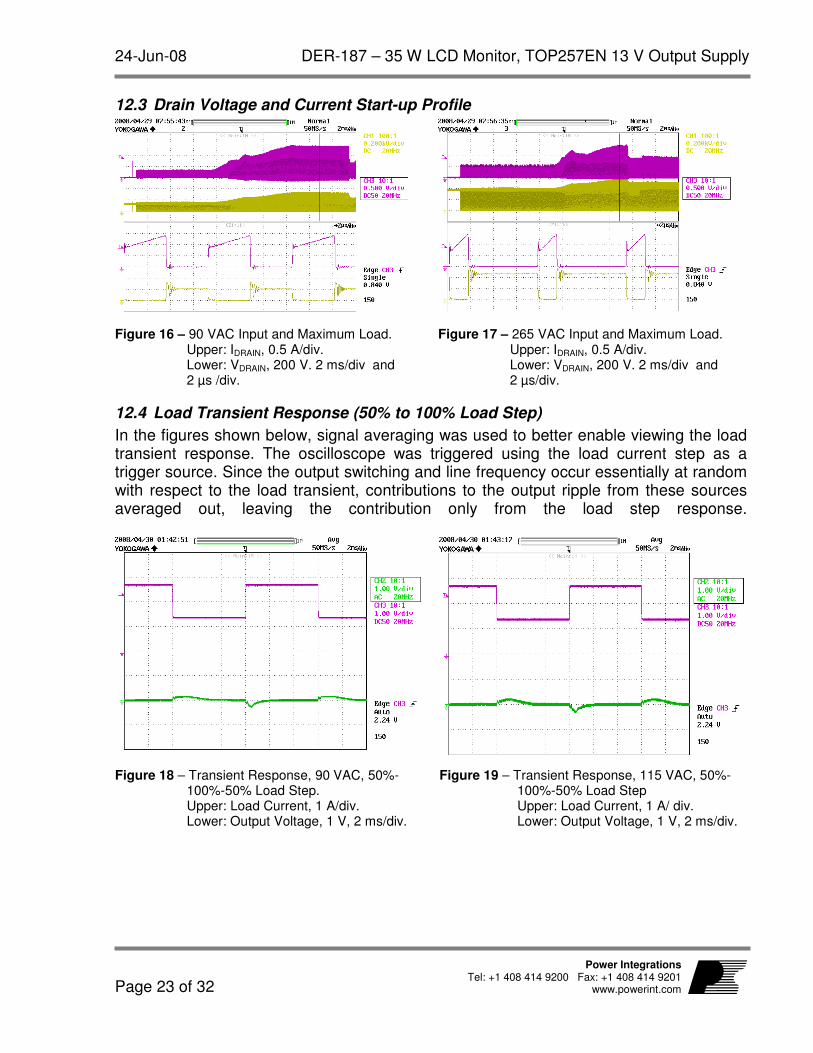
12.3 Drain Voltage and Current Start-up Profile
Figure 16 – 90 VAC Input and Maximum Load. Upper: IDRAIN, 0.5 A/div. Lower: VDRAIN, 200 V. 2 ms/div and 2 µs /div.
Figure 17 – 265 VAC Input and Maximum Load. Upper: IDRAIN, 0.5 A/div. Lower: VDRAIN, 200 V. 2 ms/div and 2 µs/div.
12.4 Load Transient Response (50% to 100% Load Step)
In the figures shown below, signal averaging was used to better enable viewing the load transient response. The oscilloscope was triggered using the load current step as a trigger source. Since the output switching and line frequency occur essentially at random with respect to the load transient, contributions to the output ripple from these sources averaged out, leaving the contribution only from the load step response.
Figure 18 – Transient Response, 90 VAC, 50%-100%-50% Load Step. Upper: Load Current, 1 A/div. Lower: Output Voltage, 1 V, 2 ms/div.
Figure 19 – Transient Response, 115 VAC, 50%-100%-50% Load Step Upper: Load Current, 1 A/ div. Lower: Output Voltage, 1 V, 2 ms/div.

DER-187 – 35 W LCD Monitor, TOP257EN 13 V Output Supply 24-Jun-08
Page 24 of 32
Power Integrations Tel: +1 408 414 9200 Fax: +1 408 414 9201 www.powerint.com
Figure 20 – Transient Response, 230 VAC, 50%-100%-50% Load Step. Upper: Load Current, 1 A/div. Lower: Output Voltage, 1 V, 2 ms/div.
12.5 Open-loop Protection
Optocoupler U2A was shorted, which opened the control loop. The output voltage was measured at no load (which is the worst-case condition for this test). Results are shown below.
Figure 21 – Output Voltage, Open-loop Test. Vin = 264 VAC.

24-Jun-08 DER-187 – 35 W LCD Monitor, TOP257EN 13 V Output Supply
Page 25 of 32
Power Integrations Tel: +1 408 414 9200 Fax: +1 408 414 9201
www.powerint.com
12.6 Output Ripple Measurements
12.6.1 Ripple Measurement Technique
For DC output ripple measurements, use a modified oscilloscope test probe to reduce spurious signals. Details of the probe modification are provided in figures below. Tie two capacitors in parallel across the probe tip of the 4987BA probe adapter. Use a
0.1 µF/50 V ceramic capacitor and a 1.0 µF/50 V aluminum-electrolytic capacitor. The aluminum-electrolytic capacitor is polarized, so always maintain proper polarity across DC outputs.
Figure 22 – Oscilloscope Probe Prepared for Ripple Measurement. (End Cap and Ground Lead Removed)
Figure 23 – Oscilloscope Probe with Probe Master 4987BA BNC Adapter. (Modified with wires for probe ground for ripple measurement, and two parallel decoupling capacitors added)
Probe Ground
Probe Tip

DER-187 – 35 W LCD Monitor, TOP257EN 13 V Output Supply 24-Jun-08
Page 26 of 32
Power Integrations Tel: +1 408 414 9200 Fax: +1 408 414 9201 www.powerint.com
12.6.2 Measurement Results
Figure 24 – Ripple, 90 VAC, Full Load. 2 ms, 50 mV/div.
Figure 25 – Ripple, 115 VAC, Full Load. 2 ms, 50 mV/div.
Figure 26 – Ripple, 230 VAC, Full Load. 2 ms, 50 mV/div.

24-Jun-08 DER-187 – 35 W LCD Monitor, TOP257EN 13 V Output Supply
Page 27 of 32
Power Integrations Tel: +1 408 414 9200 Fax: +1 408 414 9201
www.powerint.com
13 Control Loop Measurements
Figure 27 – Gain-phase Plot, 90 VAC, Maximum Steady-state Load.
Vertical Scale: Gain = 10 dB/div, Phase = 30 °/div.
Crossover Frequency = 800 Hz, Phase Margin = 60°.
Figure 28 – Gain-phase Plot, 115 VAC, Maximum Steady-state Load. Vertical Scale: Gain = 10 dB/div, Phase = 30 °/div.
Crossover Frequency = 1.0 kHz, Phase Margin = 60°.

DER-187 – 35 W LCD Monitor, TOP257EN 13 V Output Supply 24-Jun-08
Page 28 of 32
Power Integrations Tel: +1 408 414 9200 Fax: +1 408 414 9201 www.powerint.com
Figure 29 – Gain-phase Plot, 230 VAC, Maximum Steady-state Load. Vertical Scale: Gain = 10 dB/div, Phase = 30 °/div.
Crossover Frequency = 400 Hz, Phase Margin = 60°.
These results show the supply is always stable. The worst case phase margin is 60°. The gain margin is in excess of 10 dB.

24-Jun-08 DER-187 – 35 W LCD Monitor, TOP257EN 13 V Output Supply
Page 29 of 32
Power Integrations Tel: +1 408 414 9200 Fax: +1 408 414 9201
www.powerint.com
14 Line Surge
A single test unit underwent IEC61000-4-5 differential input line 1.2/50 µs surge testing. The input voltage was set to 230 VAC with a 60 Hz frequency. The output was driving a full load, and operation was verified following each surge event.
Surge Level (V)
Input Voltage (VAC)
Injection Location
Injection Phase (°)
Test Result (Pass/Fail)
Generator Output
Impedance (Ω)
+250 230 L to N 90 Pass 2 -250 230 L to N 270 Pass 2
+500 230 L to N 90 Pass 2
-500 230 L to N 270 Pass 2
+750 230 L to N 90 Pass 2
-750 230 L to N 270 Pass 2
+1000 230 L to N 90 Pass 2
-1000 230 L to N 270 Pass 2
+500 230 L and N to PE 90 Pass 12
-500 230 L and N to PE 270 Pass 12
+1000 230 L and N to PE 90 Pass 12
-1000 230 L and N to PE 270 Pass 12
+1500 230 L and N to PE 90 Pass 12
-1500 230 L and N to PE 270 Pass 12
+2000 230 L and N to PE 90 Pass 12
-2000 230 L and N to PE 270 Pass 12
The unit passed under all test conditions.

DER-187 – 35 W LCD Monitor, TOP257EN 13 V Output Supply 24-Jun-08
Page 30 of 32
Power Integrations Tel: +1 408 414 9200 Fax: +1 408 414 9201 www.powerint.com
15 Conducted EMI
Figure 30 – Conducted EMI, Maximum Steady-state Load, 115 VAC, 60 Hz, EN55022 B Limits.
Figure 31 – Conducted EMI, Maximum Steady-state Load, 230 VAC, 60 Hz, EN55022 B Limits.

24-Jun-08 DER-187 – 35 W LCD Monitor, TOP257EN 13 V Output Supply
Page 31 of 32
Power Integrations Tel: +1 408 414 9200 Fax: +1 408 414 9201
www.powerint.com
16 Revision History
Date Author Revision Description and changes Reviewed 24-Jun-08 SGK 1.0 Initial Release JD

DER-187 – 35 W LCD Monitor, TOP257EN 13 V Output Supply 24-Jun-08
Page 32 of 32
Power Integrations Tel: +1 408 414 9200 Fax: +1 408 414 9201 www.powerint.com
For the latest updates, visit our website: www.powerint.com
Power Integrations reserves the right to make changes to its products at any time to improve reliability or
manufacturability. Power Integrations does not assume any liability arising from the use of any device or circuit
described herein. POWER INTEGRATIONS MAKES NO WARRANTY HEREIN AND SPECIFICALLY DISCLAIMS ALL
WARRANTIES INCLUDING, WITHOUT LIMITATION, THE IMPLIED WARRANTIES OF MERCHANTABILITY,
FITNESS FOR A PARTICULAR PURPOSE, AND NON-INFRINGEMENT OF THIRD PARTY RIGHTS.
PATENT INFORMATION
The products and applications illustrated herein (including transformer construction and circuits external to the products)
may be covered by one or more U.S. and foreign patents, or potentially by pending U.S. and foreign patent applications
assigned to Power Integrations. A complete list of Power Integrations’ patents may be found at www.powerint.com.
Power Integrations grants its customers a license under certain patent rights as set forth at
http://www.powerint.com/ip.htm.
The PI Logo, TOPSwitch, TinySwitch, LinkSwitch, DPA-Switch, PeakSwitch, EcoSmart, Clampless, E-Shield, Filterfuse, StackFET,
PI Expert and PI FACTS are trademarks of Power Integrations, Inc. Other trademarks are property of their respective
companies. ©Copyright 2008 Power Integrations, Inc.
Power Integrations Worldwide Sales Support Locations
WORLD HEADQUARTERS 5245 Hellyer Avenue San Jose, CA 95138, USA. Main: +1-408-414-9200 Customer Service: Phone: +1-408-414-9665 Fax: +1-408-414-9765 e-mail: [email protected]
GERMANY Rueckertstrasse 3 D-80336, Munich Germany Phone: +49-89-5527-3911 Fax: +49-89-5527-3920 e-mail: [email protected]
JAPAN Kosei Dai-3 Bldg., 2-12-11, Shin-Yokohama, Kohoku-ku, Yokohama-shi, Kanagawa 222-0033 Phone: +81-45-471-1021 Fax: +81-45-471-3717 e-mail: [email protected]
TAIWAN 5F, No. 318, Nei Hu Rd., Sec. 1 Nei Hu Dist. Taipei, Taiwan 114, R.O.C. Phone: +886-2-2659-4570 Fax: +886-2-2659-4550 e-mail: [email protected]
CHINA (SHANGHAI) Rm 1601/1610, Tower 1, Kerry Everbright City No. 218 Tianmu Road West, Shanghai, P.R.C. 200070 Phone: +86-21-6354-6323 Fax: +86-21-6354-6325 e-mail: [email protected]
INDIA #1, 14
th Main Road
Vasanthanagar Bangalore-560052 India Phone: +91-80-41138020 Fax: +91-80-41138023 e-mail: [email protected]
KOREA RM 602, 6FL Korea City Air Terminal B/D, 159-6 Samsung-Dong, Kangnam-Gu, Seoul, 135-728, Korea Phone: +82-2-2016-6610 Fax: +82-2-2016-6630 e-mail: [email protected]
UNITED KINGDOM 1st Floor, St. James’s House East Street, Farnham Surrey, GU9 7TJ United Kingdom Phone: +44 (0) 1252-730-141 Fax: +44 (0) 1252-727-689 e-mail: [email protected]
CHINA (SHENZHEN) Rm A, B & C 4
th Floor, Block C,
Electronics Science and Technology Building, 2070 Shennan Zhong Rd, Shenzhen, Guangdong, China, 518031 Phone: +86-755-8379-3243 Fax: +86-755-8379-5828 e-mail: [email protected]
ITALY Via De Amicis 2 20091 Bresso MI – Italy Phone: +39-028-928-6000 Fax: +39-028-928-6009 e-mail: [email protected]
SINGAPORE 51 Newton Road, #15-08/10 Goldhill Plaza, Singapore, 308900 Phone: +65-6358-2160 Fax: +65-6358-2015 e-mail: [email protected]
APPLICATIONS HOTLINE World Wide +1-408-414-9660 APPLICATIONS FAX World Wide +1-408-414-9760