Design Example Report - Power · Design Example Report Title ... High active mode efficiency: ......
28
Power Integrations 5245 Hellyer Avenue, San Jose, CA 95138 USA. Tel: +1 408 414 9200 Fax: +1 408 414 9201 www.powerint.com Design Example Report Title 3 W Single Output, <10 mW No-load Consumption, Isolated Adapter Using LinkSwitch-XT Specification 85 VAC – 265 VAC Input; 5 V, 0.6 A, CV Output Application General Purpose Adapter Author Applications Engineering Department Document Number DER-227 Date October 6, 2009 Revision 1.1 Summary and Features Universal Input: 85 to 265 VAC EcoSmart® – Easily meets all current international energy efficiency standards - China (CECP) / CEC / ENERGY STAR 2 / EU CoC Extremely low no-load input power consumption: <10 mW at 230 VAC EC IPP rating of 5 out of 5 stars High active mode efficiency: >70 % o Exceeds 64% ENERGY STAR v2, EC CoC v4 and EuP Tier 2 requirements Meets EN55022B/CISPR22B conducted EMI limits without a Y-capacitor across the isolation barrier PATENT INFORMATION The products and applications illustrated herein (including transformer construction and circuits external to the products) may be covered by one or more U.S. and foreign patents, or potentially by pending U.S. and foreign patent applications assigned to Power Integrations. A complete list of Power Integrations' patents may be found at www.powerint.com. Power Integrations grants its customers a license under certain patent rights as set forth at <http://www.powerint.com/ip.htm>.
Transcript of Design Example Report - Power · Design Example Report Title ... High active mode efficiency: ......

Power Integrations
5245 Hellyer Avenue, San Jose, CA 95138 USA. Tel: +1 408 414 9200 Fax: +1 408 414 9201
www.powerint.com
Design Example Report
Title 3 W Single Output, <10 mW No-load Consumption, Isolated Adapter Using LinkSwitch-XT
Specification 85 VAC – 265 VAC Input; 5 V, 0.6 A, CV Output
Application General Purpose Adapter
Author Applications Engineering Department
Document Number
DER-227
Date October 6, 2009
Revision 1.1
Summary and Features Universal Input: 85 to 265 VAC EcoSmart® – Easily meets all current international energy efficiency standards -
China (CECP) / CEC / ENERGY STAR 2 / EU CoC Extremely low no-load input power consumption: <10 mW at 230 VAC EC IPP rating of 5 out of 5 stars High active mode efficiency: >70 %
o Exceeds 64% ENERGY STAR v2, EC CoC v4 and EuP Tier 2 requirements Meets EN55022B/CISPR22B conducted EMI limits without a Y-capacitor across the
isolation barrier PATENT INFORMATION The products and applications illustrated herein (including transformer construction and circuits external to the products) may be covered by one or more U.S. and foreign patents, or potentially by pending U.S. and foreign patent applications assigned to Power Integrations. A complete list of Power Integrations' patents may be found at www.powerint.com. Power Integrations grants its customers a license under certain patent rights as set forth at <http://www.powerint.com/ip.htm>.

DER-227 3 W Adapter – LNK363DN 6-Oct-09
Page 2 of 28
Power Integrations Tel: +1 408 414 9200 Fax: +1 408 414 9201 www.powerint.com
Table of Contents 1 Introduction.................................................................................................................3 2 Power Supply Specification ........................................................................................4 3 Schematic...................................................................................................................5 4 Circuit Description ......................................................................................................6
4.1 Input Rectification and EMI Filtering....................................................................6 4.2 LinkSwitch Primary..............................................................................................6 4.3 Output Rectification .............................................................................................6 4.4 Output Feedback.................................................................................................7 4.5 Primary Bias Circuit .............................................................................................7 4.6 Design for low no-load consumption ...................................................................7
5 PCB Layout ................................................................................................................8 6 Bill of Materials ...........................................................................................................9 7 Transformer Design..................................................................................................10
7.1 Electrical Diagram .............................................................................................10 7.2 Electrical Specifications.....................................................................................10 7.3 Material..............................................................................................................10 7.4 Transformer Build Diagram ...............................................................................11 7.5 Transformer Construction..................................................................................11
8 Transformer Design Spreadsheet.............................................................................12 9 Performance Data ....................................................................................................14
9.1 Efficiency ...........................................................................................................14 9.1.1 Active Mode Efficiency ...............................................................................14
9.2 No-load Input Power..........................................................................................15 9.3 Regulation .........................................................................................................16 9.4 Available Standby Output Power.......................................................................17
10 Waveforms............................................................................................................18 10.1 Drain Voltage and Current, Normal Operation...................................................18 10.2 Output Voltage Start-up Profile..........................................................................19 10.3 Drain Voltage Start-up Profile............................................................................19 10.4 Load Transient Response (50% to 100% Load Step) .......................................20 10.5 Thermal Performance........................................................................................21 10.6 Output Ripple Measurements............................................................................23
10.6.1 Ripple Measurement Technique ................................................................23 10.6.2 Measurement Results ................................................................................24
11 Conducted EMI .....................................................................................................25 11.1 115 VAC, Full load ............................................................................................25 11.2 230 VAC, Full load ............................................................................................26
12 Revision History ....................................................................................................27 Important Note: Although this board is designed to satisfy safety isolation requirements, the engineering prototype has not been agency approved. Therefore, all testing should be performed using an isolation transformer to provide the AC input to the prototype board.

6-Oct-09 DER-227 3 W Adapter – LNK363DN
Page 3 of 28
Power Integrations Tel: +1 408 414 9200 Fax: +1 408 414 9201
www.powerint.com
1 Introduction This document is an engineering report describing a 5 V, 0.6 A power supply utilizing the LNK363DN (SO8 package) from the LinkSwitch-XT family. It contains the power supply specification, schematic, bill of materials, transformer documentation, printed circuit layout, and performance data. This design highlights the ultra low no-load input power consumption that is possible when using a LinkSwitch-XT device.
Figure 1 – Populated Circuit Board Photograph.

DER-227 3 W Adapter – LNK363DN 6-Oct-09
Page 4 of 28
Power Integrations Tel: +1 408 414 9200 Fax: +1 408 414 9201 www.powerint.com
2 Power Supply Specification The table below represents the minimum acceptable performance of the design. Actual performance is listed in the results section.
Description Symbol Min Typ Max Units Comment
Input Voltage VIN 85 265 VAC 2 Wire – no P.E.
Frequency fLINE 47 50/60 64 Hz
No-load Input Power (230 VAC) 0.02 W
Output
Output Voltage VOUT(CV) 4.75 5.00 5.25 V Measured at PCB terminal
Output Ripple Voltage VRIPPLE 250 mV 20 MHz bandwidth
Output Current IOUT1 0.5 0.55 0.6 A In CC Mode
Total Output Power
Continuous Output Power POUT 3 W
Efficiency
Full Load 59 % Measured at Full Load 25 oC
Required average efficiency at 25, 50, 75 and 100 % of POUT CEC 64 % Per ENERGY STAR test method
Environmental
Conducted EMI Meets CISPR22B / EN55022B Output floating or earth grounded
Safety Designed to meet IEC950, UL1950 Class II
Ambient Temperature TAMB -10 40 oC Free convection, sea level, enclosed adapter
Figure 2 – Output Characteristic Limits.

6-Oct-09 DER-227 3 W Adapter – LNK363DN
Page 5 of 28
Power Integrations Tel: +1 408 414 9200 Fax: +1 408 414 9201
www.powerint.com
3 Schematic
Figure 3 – Schematic.

DER-227 3 W Adapter – LNK363DN 6-Oct-09
Page 6 of 28
Power Integrations Tel: +1 408 414 9200 Fax: +1 408 414 9201 www.powerint.com
4 Circuit Description The Flyback power supply shown in Figure 3 was designed around the LNK363DN (U1). The output voltage is sensed and feed back to U1 through optocoupler U2. That feedback is used by U1 to maintain constant voltage (CV) regulation of the output.
4.1 Input Rectification and EMI Filtering Diodes D1-D4 rectify the AC input voltage. Capacitors C1 and C2 filter the rectified AC input voltage and provide a high voltage DC bus which is connected to pin 1 of the transformer. Inductor L1 and ferrite bead L2 are used to provide differential mode filtering for conducted EMI compliance.
4.2 LinkSwitch Primary The LNK363DN device integrates the oscillator, controller, startup and other protection circuitry as well as the high voltage MOSFET on a single monolithic IC. Suffix D indicates the SO-8 package and the second suffix N indicates lead-free RoHS compliant device. The LNK363DN operates at a fixed current limit (ILIMIT). Every enabled switching cycle the primary current ramps to this current limit level. Output regulation is maintained by skipping switching cycles (ON/OFF control). The internal controller determines if the next switching cycle should be enabled or disabled (skipped) based on the current flowing into the FEEDBACK (FB) pin. If a current less than 49 µA flows into the FB pin when the oscillator’s (internal) clock signal occurs, MOSFET switching is enabled for that particular switching cycle and the MOSFET turns on. If the current is greater than 49 µA then the MOSFET is disabled for the current switching cycle. The switching cycle terminates when the current through the MOSFET reaches ILIMIT, or the on-time of the MOSFET reaches the maximum duty cycle (DCMAX) limit. At full load, few switching cycles will be skipped (disabled), resulting in a high effective switching frequency. As the load reduces, more switching cycles are skipped, which reduces the effective switching frequency. At no-load, most switching cycles are skipped, which is what makes the no-load power consumption of supplies designed around the LinkSwitch-XT family so low, since switching losses are the dominant loss mechanism at light loading. Additionally, since the amount of energy per switching cycle is fixed by ILIMIT, the skipping of switching cycles gives the supply a flat efficiency characteristic over the load range.
4.3 Output Rectification Diode D5 rectifies the output from transformer T1. This rectifier is a low drop Schottky diode. Output filtering was provided by capacitor C6 which is a super low ESR type to reduce output ripple and remove the need for a LC second stage switching noise filter.

6-Oct-09 DER-227 3 W Adapter – LNK363DN
Page 7 of 28
Power Integrations Tel: +1 408 414 9200 Fax: +1 408 414 9201
www.powerint.com
4.4 Output Feedback The output voltage (CV portion) is regulated by the LMV431 (U2), which is a 1%, 1.24 V reference shunt regulator. Resistors R6 and R8, both 1% resistors, program the output voltage to 5 V. Resistor R7 and C7 provide loop compensation. A feedback current proportional to the output voltage flows through the optocoupler diode (U3A). On the primary side, phototransistor (U3B) delivers this feedback current into the FB pin. Just before the start of each cycle, the LinkSwitch-XT controller checks this FB pin current, to determine if the next switching cycle is enabled or disabled.
4.5 Primary Bias Circuit LinkSwitch-XT devices do not require an external bias supply for operation and can be configured to be self powered. However providing the operating current for the device into the BYPASS (BP) pin externally dramatically reduces no load input power. In this design the bias winding (pins 3 and 4 on the transformer) output is rectified and filtered by D7 and C8. The value of C8 was selected to give an acceptable minimum voltage during no-load when the supply is operating at low switching frequencies. Resistor R11 is selected such that approximately 200 A to 250 A flows into the BP pin.
4.6 Design for low no-load consumption In addition to the addition of a bias circuit the following design choices were made to reduce no-load input power Zener bleed primary clamp (VR1, R12, C3, R2, D6)
Typically for this type of design a RCD clamp would be used (VR1 replaced with a zero ohm jumper). However at low switching frequencies the voltage across the capacitor (C3) can discharge below the reflected output voltage making the clamp appear as a load and increasing input power. The addition of VR1 prevents this by limiting the minimum voltage across C3 falling below the voltage rating of VR1.
Use of TLV431 vs. TL431 (U2) The TLV431 reference requires a bias current of 100 A vs. 1 mA for the TLV431. This reduces input power at no-load by ~20 mW (including effect of efficiency).
High gain optocoupler (U3) The use of a high gain optocoupler reduces no-load input power by reducing the current through the optocoupler and hence loading of the output.
DER-227 3 W Adapter – LNK363DN 6-Oct-09
Page 8 of 28
Power Integrations Tel: +1 408 414 9200 Fax: +1 408 414 9201 www.powerint.com
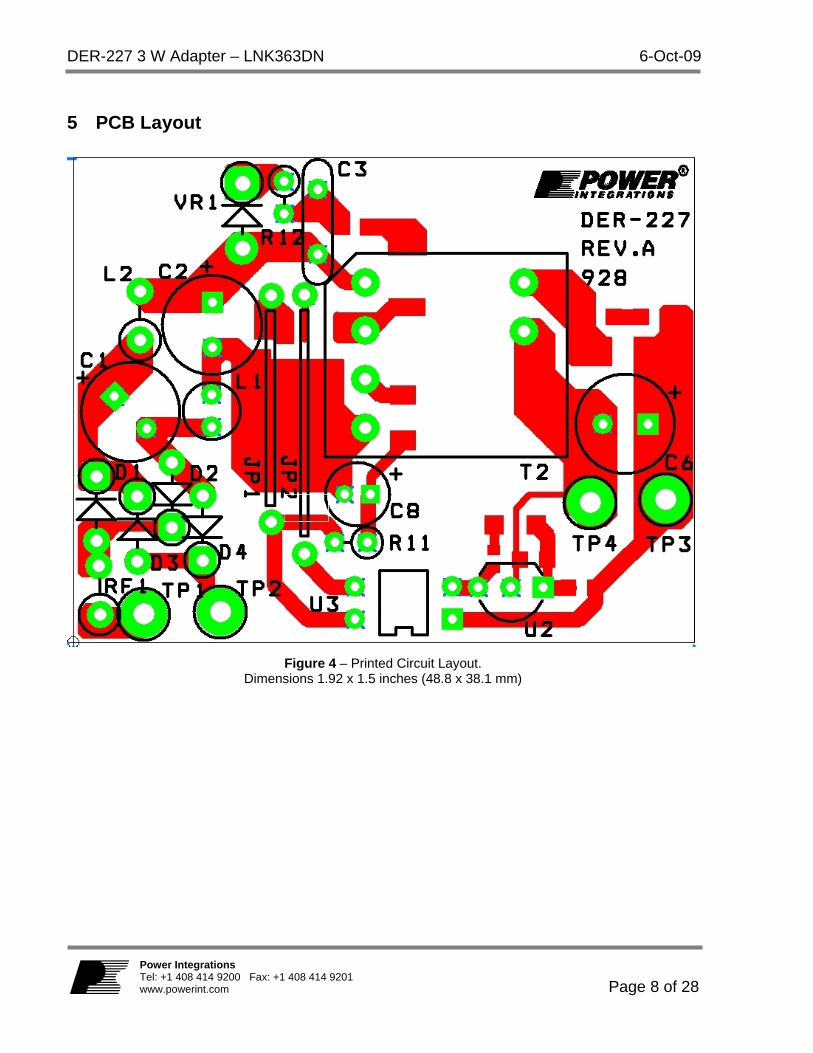
5 PCB Layout
Figure 4 – Printed Circuit Layout.
Dimensions 1.92 x 1.5 inches (48.8 x 38.1 mm)

6-Oct-09 DER-227 3 W Adapter – LNK363DN
Page 9 of 28
Power Integrations Tel: +1 408 414 9200 Fax: +1 408 414 9201
www.powerint.com
6 Bill of Materials
Item Ref Des Qty Description Mfg Part Number Mfg
1 2 C1 C2 4.7 F, 400 V, Electrolytic, (8 x 11.5) TAQ2G4R7MK0811MLL3 Taicon Corporation
2 1 C3 10 nF, 630 V, Film ECQ-E6103KF Panasonic
3 1 C4 100 nF, 50 V, Ceramic, X7R, 0805 ECJ-2YB1H104K Panasonic
4 1 C5 1 nF, 50 V, Ceramic, X7R, 0805 ECJ-2VB1H102K Panasonic
5 1 C6 1000 F, 10 V, Electrolytic, Low ESR, (8 x 16) 10MCZ1000M8X16 Rubycon
6 1 C7 100 nF, 50 V, Ceramic, X7R, 1206 ECJ-3VB1H104K Panasonic
7 1 C8 33 F, 35 V, Electrolytic, Low ESR, 50 m, (5 x 11.5) ELXZ350ELL330MEB5D Nippon Chemi-Con
8 4 D1 D2 D3 D4 1000 V, 1 A, Rectifier, DO-41 1N4007 Vishay
9 1 D5 40 V, 1 A, Schottky, DO-214AC SS14 Vishay
10 1 D6 1000 V, 1 A, Rectifier, MELF DL4007 Diodes Inc
11 1 D7 75 V, 0.15 A, Fast Switching, 4 ns, MELF LL4148-13 Diode Inc.
12 1 JP1 Wire Jumper, Non insulated, 22 AWG, 0.7 in 298 Alpha
13 1 JP2 Wire Jumper, Non insulated, 22 AWG, 0.6 in 298 Alpha
14 1 L1 1 mH, 0.15 A, Ferrite Core SBCP-47HY102B Tokin
15 1 L2 3.5 mm x 4.45 mm, 56 at 100 MHz, 22 AWG hole, Ferrite Bead 2761001112 Fair-Rite
16 1 R2 330 , 5%, 1/8 W, Metal Film, 0805 ERJ-6GEYJ331V Panasonic
17 1 R3 16 , 5%, 1/8 W, Metal Film, 0805 ERJ-6GEYJ160V Panasonic
18 1 R6 301 k, 1%, 1/8 W, Metal Film, 0805 ERJ-6ENF3013V Panasonic
19 1 R7 1 k, 5%, 1/10 W, Metal Film, 0603 ERJ-3GEYJ102V Panasonic
20 1 R8 100 k, 1%, 1/8 W, Metal Film, 0805 ERJ-6ENF1003V Panasonic
21 1 R11 14.3 k, 1%, 1/4 W, Metal Film MFR-25FBF-14K3 Yageo
22 1 R12 51 k, 5%, 1/4 W, Metal Film ERJ-3GEYJ512V Yageo
23 1 RF1 8.2 , 2 W, Fusible/Flame Proof Wire Wound CRF253-4 5T 8R2 Vitrohm
24 1 T2 Bobbin, EE13, Horizontal, 8 pins 548 Hical Magnetics
25 1 TP1 Test Point, WHT,THRU-HOLE MOUNT 5012 Keystone
26 2 TP2 TP4 Test Point, BLK,THRU-HOLE MOUNT 5011 Keystone
27 1 TP3 Test Point, RED,THRU-HOLE MOUNT 5010 Keystone
28 1 U1 LinkSwitch-XT, LNK363DN, SO-8-DN LNK363DN Power Integrations
29 1 U2 1.24V Shunt Reg IC LMV431ACZ National Semiconductor
30 1 U3 Opto coupler, 35 V, CTR 80-160%, 4-DIP PC817X1 Sharp
31 1 VR1 68 V, 5%, 5 W, DO-41 1N5373BG ON Semiconductor
Note: Parts listed above are RoHS Compliant

DER-227 3 W Adapter – LNK363DN 6-Oct-09
Page 10 of 28
Power Integrations Tel: +1 408 414 9200 Fax: +1 408 414 9201 www.powerint.com
7 Transformer Design
7.1 Electrical Diagram
Figure 5 – Transformer Electrical Diagram.
7.2 Electrical Specifications Electrical Strength 60 seconds, 60 Hz, from pins 1-4 to pins 7-8. 3000 VAC Primary Inductance Pins 1-2, all other windings open. 1620 H, -/+10%Resonant Frequency Pins 1-2, all other windings open. 540 kHz (Min.) Primary Leakage Inductance Pins 1-2, pins 3-4, pins 7-8 shorted. 140 H (Max.)
7.3 Material Item Description [1] Core: PC44 EE13 Gapped for 64 nH/T2. [2] Bobbin: EE13, Horizontal, Hical Magnetics 548. [3] Magnet wire: #37 AWG, double coated. [4] Triple insulated: #26 AWG. [5] Magnet wire: #26 AWG, double coated. [6] Tape: 3M 1298 Polyester Film, 2 mils thick, 7.5mm wide. [7] Copper tape 2 mil thick. [8] Varnish.
2
3
Cancellation
Bias
Primary
159T #37 AWG
WDG # 3
WDG # 1
24T #26 AWG
WDG # 2
27T #37 AWG X2
4
1 8
7
Secondary
11T #26 T.I.W WDG # 4

6-Oct-09 DER-227 3 W Adapter – LNK363DN
Page 11 of 28
Power Integrations Tel: +1 408 414 9200 Fax: +1 408 414 9201
www.powerint.com
7.4 Transformer Build Diagram
Figure 6 – Transformer Build Diagram.
7.5 Transformer Construction Bobbin
Preparation Place the bobbin [2] with primary pins on the left hand side. Winding direction is clockwise direction.
Winding 1: Shield
Start at pin 1, wind 27 bifilar turns of item [3] from left to right. Wind with tight tension across entire bobbin evenly in a single uniform layer, and cut the finish end – leave floating.
Insulation 1 layer of tape, item [6] for insulation.
Winding 2: Primary
Start at pin 2, wind 53 turns of item [3] from left to right , 1 layer of tape, item [6], continue wind another 53 turns from right to left, 1 layer of tape, item [6], continue wind another 53 turns from left to right. Place the wire with tight tension across the bobbin evenly in a uniform winding. Terminate on pin 1.
Insulation 1 layer of tape, item [6] for insulation.
Winding 3: Bias
Start at pin 4, wind 16 turns of item [5] from left to right with tight tension, 1 layer of tape, item [6], continue wind another 8 turns from right to left, and terminate at pin 3. Cut the start end. Wind with tight tension across the bobbin evenly for all these three layers.
Insulation 1 layer of tape, item [6] for insulation. Winding 4: Secondary
Start at pin 8, wind 11 turns of item [4] from right to left with tight tension in a uniform winding. Terminate at pin 7. Wind with tight tension across the bobbin evenly.
Insulation 3 layer of tape, item [6] for insulation.
Flux band Construct a flux band by wrapping a single shorted turn of item [7] around the outside of windings and core halves with tight tension. Make an electrical connection to pin(s) 1 using wire.
Finish Dip Varnish in item [8] – do not vacuum impregnate due to higher capacitance.
1 No Connect
Primary Winding
Bias Winding
Cancellation Winding
2
4
1 Layer of Tape
3
7
8
1 Layer of Tape
1
Secondary Winding 11Ts

DER-227 3 W Adapter – LNK363DN 6-Oct-09
Page 12 of 28
Power Integrations Tel: +1 408 414 9200 Fax: +1 408 414 9201 www.powerint.com
8 Transformer Design Spreadsheet ACDC_LinkSwitch-
XT_021307; Rev.1.20; Copyright Power Integrations 2007 INPUT INFO OUTPUT UNIT
ACDC_LinkSwitch-XT_021307_Rev1-20.xls; LinkSwitch-XT Continuous/Discontinuous Flyback Transformer Design Spreadsheet
ENTER APPLICATION VARIABLES VACMIN 85 Volts Minimum AC Input Voltage VACMAX 265 Volts Maximum AC Input Voltage fL 50 Hertz AC Mains Frequency
VO 5.00 Volts Output Voltage (main) (For CC designs enter upper CV tolerance limit)
IO 0.60 Amps Power Supply Output Current (For CC designs enter upper CC tolerance limit)
CC Threshold Voltage 0.00 Volts Voltage drop across sense resistor.
Output Cable Resistance 0.00 0.00 Ohms Enter the resistance of the output cable (if used)
PO 3.00 Watts Output Power (VO x IO + CC dissipation)
Feedback Type Opto Opto
Choose 'BIAS' for Bias winding feedback and 'OPTO' for Optocoupler feedback from the 'Feedback Type' drop down box at the top of this spreadsheet
Add Bias Winding yes Yes
Choose 'YES' in the 'Bias Winding' drop down box at the top of this spreadsheet to add a Bias winding. Choose 'NO' to continue design without a Bias winding. Addition of Bias winding can lower no load consumption
Clampless design (LNK 362 only)
NO External Clamp
Choose 'YES' from the 'clampless Design' drop down box at the top of this spreadsheet for a clampless design. Choose 'NO' to add an external clamp circuit. Clampless design lowers the total cost of the power supply
n 0.7 Efficiency Estimate at output terminals.
Z 0.50 0.5 Loss Allocation Factor (suggest 0.5 for CC=0 V, 0.75 for CC=1 V)
tC 2.90 mSeconds Bridge Rectifier Conduction Time Estimate CIN 9.40 uFarads Input Capacitance
Input Rectification Type F F Choose H for Half Wave Rectifier and F for Full Wave Rectification from the 'Rectification' drop down box at the top of this spreadsheet
ENTER LinkSwitch-XT VARIABLES
LinkSwitch-XT LNK363 LNK363
User selection for LinkSwitch-XT. Ordering info - Suffix P/G indicates DIP 8 package; suffix D indicates SO8 package; second suffix N indicates lead free RoHS compliance
Chosen Device LNK363 ILIMITMIN 0.195 Amps Minimum Current Limit ILIMITMAX 0.225 Amps Maximum Current Limit fSmin 124000 Hertz Minimum Device Switching Frequency
I^2fmin 4948 A^2Hz I^2f (product of current limit squared and frequency is trimmed for tighter tolerance)
VOR 83.00 83 Volts Reflected Output Voltage
VDS 10 Volts LinkSwitch-XT on-state Drain to Source Voltage
VD 0.75 0.75 Volts Output Winding Diode Forward Voltage Drop
KP 1.07 Ripple to Peak Current Ratio (0.6 < KP < 6.0). For Clampless Designs use KP > 1.1
ENTER TRANSFORMER CORE/CONSTRUCTION VARIABLES Core Type EE13 EE13 User-Selected transformer core Core EE13 P/N: PC40EE13-Z Bobbin EE13_
BOBBIN
P/N: EE13_BOBBIN
AE 0.171 cm^2 Core Effective Cross Sectional Area LE 3.02 cm Core Effective Path Length

6-Oct-09 DER-227 3 W Adapter – LNK363DN
Page 13 of 28
Power Integrations Tel: +1 408 414 9200 Fax: +1 408 414 9201
www.powerint.com
AL 1130 nH/T^2 Ungapped Core Effective Inductance BW 7.9 mm Bobbin Physical Winding Width M 0 mm Safety Margin Width (Half the Primary to Secondary
Creepage Distance) L 3.00 3 Number of Primary Layers NS 11 11 Number of Secondary Turns NB 24 24 Number of Bias winding turns VB 12.55 Volts Bias Winding voltage PIVB 74 Volts Bias Diode Maximum Peak Inverse Voltage
DC INPUT VOLTAGE PARAMETERS VMIN 89 Volts Minimum DC Input Voltage VMAX 375 Volts Maximum DC Input Voltage CURRENT WAVEFORM SHAPE PARAMETERS DMAX 0.49 Maximum Duty Cycle IAVG 0.05 Amps Average Primary Current IP 0.1950 Amps Minimum Peak Primary Current IR 0.1950 Amps Primary Ripple Current IRMS 0.08 Amps Primary RMS Current TRANSFORMER PRIMARY DESIGN PARAMETERS LP 1620 uHenries Typical Primary Inductance. +/- 10% LP_TOLERANCE 10.00 10 % Primary inductance tolerance
NP 159 Primary Winding Number of Turns ALG 64 nH/T^2 Gapped Core Effective Inductance BM 1342 Gauss Maximum Operating Flux Density, BM<1500 is
recommended BAC 671 Gauss AC Flux Density for Core Loss Curves (0.5 X Peak
to Peak) ur 1588 Relative Permeability of Ungapped Core LG 0.32 mm Gap Length (Lg > 0.1 mm) BWE 23.7 mm Effective Bobbin Width OD 0.149 mm Maximum Primary Wire Diameter including
insulation INS 0.03 mm Estimated Total Insulation Thickness (= 2 * film
thickness) DIA 0.115 mm Bare conductor diameter AWG 37 AWG Primary Wire Gauge (Rounded to next smaller
standard AWG value) CM 20 Cmils Bare conductor effective area in circular mils CMA 255 Cmils/A
mp Primary Winding Current Capacity (150 < CMA < 500)
TRANSFORMER SECONDARY DESIGN PARAMETERS Lumped parameters ISP 2.81 Amps Peak Secondary Current ISRMS 1.11 Amps Secondary RMS Current IRIPPLE 0.94 Amps Output Capacitor RMS Ripple Current CMS 223 Cmils Secondary Bare Conductor minimum circular mils AWGS 26 AWG Secondary Wire Gauge (Rounded up to next larger
standard AWG value) DIAS 0.41 mm Secondary Minimum Bare Conductor Diameter ODS 0.72 mm Secondary Maximum Outside Diameter for Triple
Insulated Wire INSS 0.16 mm Maximum Secondary Insulation Wall Thickness VOLTAGE STRESS PARAMETERS VDRAIN 569 Volts Maximum Drain Voltage Estimate (Includes Effect of
Leakage Inductance) PIVS 31 Volts Output Rectifier Maximum Peak Inverse Voltage

DER-227 3 W Adapter – LNK363DN 6-Oct-09
Page 14 of 28
Power Integrations Tel: +1 408 414 9200 Fax: +1 408 414 9201 www.powerint.com
9 Performance Data All measurements performed at room temperature, 60 Hz input frequency. The measurements were done at the PCB terminals.
9.1 Efficiency
60
65
70
75
0 0.06 0.12 0.18 0.24 0.3 0.36 0.42 0.48 0.54 0.6
Output Current (A)
Eff
icie
ncy
(%)
265 V
230 V115 V85 V
Figure 7 – Efficiency vs. Input Voltage, Room Temperature, 60 Hz.
9.1.1 Active Mode Efficiency
Percent of Full Load
Efficiency (%)
115 VAC 230 VAC
25 68.83 70.51 50 70.24 70.91 75 70.27 70.86 100 69.86 70.96
Average 69.80 70.81 EC CoC,
EuP Tier 2, ENERGY STAR v2 requirements (%)
64

6-Oct-09 DER-227 3 W Adapter – LNK363DN
Page 15 of 28
Power Integrations Tel: +1 408 414 9200 Fax: +1 408 414 9201
www.powerint.com
9.2 No-load Input Power
5
6
7
8
9
10
11
12
13
80 100 120 140 160 180 200 220 240 260
Input Voltage (VAC)
No
Lo
ad I
np
ut
Po
wer
(m
W)
Figure 8 – Zero Load Input Power vs. Input Line Voltage, Room Temperature, 60 Hz.

DER-227 3 W Adapter – LNK363DN 6-Oct-09
Page 16 of 28
Power Integrations Tel: +1 408 414 9200 Fax: +1 408 414 9201 www.powerint.com
9.3 Regulation
4.5
4.7
4.9
5.1
5.3
5.5
0 0.06 0.12 0.18 0.24 0.3 0.36 0.42 0.48 0.54 0.6
Output Current (A)
Ou
tpu
t vo
ltag
e (V
) 265 V230 V115 V 85 V
Figure 9 – Load and Line Regulation, Room Temperature.

6-Oct-09 DER-227 3 W Adapter – LNK363DN
Page 17 of 28
Power Integrations Tel: +1 408 414 9200 Fax: +1 408 414 9201
www.powerint.com
9.4 Available Standby Output Power The chart below shows the available output power versus line voltage at input power consumption levels of 1, 2 and 3 Watts (respectively). Again, this performance illustrates the value of ON/OFF control, as it automatically maintains a high efficiency, even during very light loading. This simplifies complying with standby requirements that specify that a fair amount of power be available to the load at low input power consumption levels. The LinkSwitch ON/OFF control scheme maximizes the amount of out power available to load in standby operation when the allowable input power is fixed at a low value. This simplifies the design of products such as printers, set-top boxes, DVD players, etc. that must meet stringent standby power consumption requirements.
0
1
2
3
85 105 125 145 165 185 205 225 245 265
Voltage Input (VAC)
Ou
tpu
t P
ow
er (
W)
Pin = 3 W
Pin = 2 W
Pin = 1 W
Figure 10 – Available Output Power for 1, 2 and 3 Watts of Input Power.

DER-227 3 W Adapter – LNK363DN 6-Oct-09
Page 18 of 28
Power Integrations Tel: +1 408 414 9200 Fax: +1 408 414 9201 www.powerint.com
10 Waveforms
10.1 Drain Voltage and Current, Normal Operation
Figure 11 – 115 VAC, Full Load.
Upper: IDRAIN, 0.1 A / div. Lower: VDRAIN, 50 V, 1 s / div.
Figure 12 – 230 VAC, Full Load. Upper: IDRAIN, 0.1 A / div. Lower: VDRAIN, 100 V, 1 s / div.
Figure 13 – 115 VAC, Full Load. VDRAIN, 50 V, 20 s / div.
Figure 14 – 230 VAC, Full Load. VDRAIN, 100 V, 20 s / div.

6-Oct-09 DER-227 3 W Adapter – LNK363DN
Page 19 of 28
Power Integrations Tel: +1 408 414 9200 Fax: +1 408 414 9201
www.powerint.com
10.2 Output Voltage Start-up Profile
Figure 15 – Start-up Profile, 115 VAC.
Slower Rise Time is Full Load Waveform.Faster Rise Time is No Load Waveform. 1 V, 5 ms / div.
Figure 16 – Start-up Profile, 230 VAC. Slower Rise Time is Full Load Waveform.Faster Rise Time is No Load Waveform. 1 V, 5 ms / div.
10.3 Drain Voltage Start-up Profile
Figure 17 – 85 VAC Input and Maximum Load. VDRAIN,50 V / div.
Figure 18 – 265 VAC Input and Maximum Load. VDRAIN, 100 V / div.

DER-227 3 W Adapter – LNK363DN 6-Oct-09
Page 20 of 28
Power Integrations Tel: +1 408 414 9200 Fax: +1 408 414 9201 www.powerint.com
10.4 Load Transient Response (50% to 100% Load Step) In the figures shown below, signal averaging was used to better enable viewing the load transient response. The oscilloscope was triggered using the load current step as a trigger source. Since the output switching and line frequency occur essentially at random with respect to the load transient, contributions to the output ripple from these sources will average out, leaving the contribution only from the load step response.
Figure 19 – Transient Response, 115 VAC,
50-100-50% Load Step. Upper: Output Voltage 500 mV / div. Lower: Load Current, 0.25 A / div.
Figure 20 – Transient Response, 230 VAC, 50-100-50% Load Step. Upper: Output Voltage 500 mV / div. Lower: Load Current, 0.25 A / div.

6-Oct-09 DER-227 3 W Adapter – LNK363DN
Page 21 of 28
Power Integrations Tel: +1 408 414 9200 Fax: +1 408 414 9201
www.powerint.com
10.5 Thermal Performance Temperature measurements of key components were taken using t-type thermocouples. The thermocouples were soldered directly to the source of LNK363DN and to the cathode of output rectifier D5 and clamp diode VR1. The thermocouple was glued to the core and winding surface of transformer T1. The unit was sealed inside a box to eliminate any air flow. The box was placed inside a thermal chamber. The ambient temperature inside the box was raised to 40 ºC. The unit was then operated at full load and the temperature measurements were taken after they stabilized for 1 hour at 40 ºC. Measurements were taken with no air flow across the power supply.
Temperature (C) Item
85 VAC 265 VAC
Ambient 40 40
Transformer (T1) 70 71.4
Clamp Diode 63 63.5
LinkSwitch-XT (U1) Source pin
81.6 85
Output Rectifier (D5) 72.9 75.2
Table 1 – Thermal Performance, Full Load.

DER-227 3 W Adapter – LNK363DN 6-Oct-09
Page 22 of 28
Power Integrations Tel: +1 408 414 9200 Fax: +1 408 414 9201 www.powerint.com
The thermal images indicate the hottest areas and components on both sides of the board and were taken to ensure that the hottest components were being monitored with thermocouples when placed in the thermal chamber. The thermal images show that the hottest point on the top side is the output diode. The hottest point on the bottom side of the board is the LinkSwitch-XT device.
Figure 21 –Thermograph of Top Layer.
Figure 22 –Thermograph of Bottom Layer.

6-Oct-09 DER-227 3 W Adapter – LNK363DN
Page 23 of 28
Power Integrations Tel: +1 408 414 9200 Fax: +1 408 414 9201
www.powerint.com
10.6 Output Ripple Measurements
10.6.1 Ripple Measurement Technique
For DC output ripple measurements, a modified oscilloscope test probe must be utilized in order to reduce spurious signals due to pickup. Details of the probe modification are provided in figures below. The 4987BA probe adapter is affixed with two capacitors tied in parallel across the probe tip. The capacitors include one (1) 0.1 F/50 V ceramic type and one (1) 1.0 F/50 V aluminum electrolytic. The aluminum electrolytic type capacitor is polarized, so proper polarity across DC outputs must be maintained (see below).
Figure 23 – Oscilloscope Probe Prepared for Ripple Measurement. (End Cap and Ground Lead Removed)
Figure 24 – Oscilloscope Probe with Probe Master (www.probemaster.com) 4987A BNC Adapter.
(Modified with wires for ripple measurement, and two parallel decoupling capacitors added)
Probe Ground
Probe Tip

DER-227 3 W Adapter – LNK363DN 6-Oct-09
Page 24 of 28
Power Integrations Tel: +1 408 414 9200 Fax: +1 408 414 9201 www.powerint.com
10.6.2 Measurement Results
Figure 25 – Output Ripple, 115 VAC, Full Load.
Figure 26 – Output Ripple, 230 VAC, Full Load.

6-Oct-09 DER-227 3 W Adapter – LNK363DN
Page 25 of 28
Power Integrations Tel: +1 408 414 9200 Fax: +1 408 414 9201
www.powerint.com
11 Conducted EMI Conducted EMI were tested with flux band at115 VAC and 230 VAC at full load, with earth connected to output return and artificial hand connected to output return. Composite EN55022B/CISPR22B conducted limits are shown. In all cases there was about 10dB margin.
11.1 115 VAC, Full load
Line Neutral
Artificial Hand Connected to Output Return.
Artificial Hand Connected to Output Return.
Output Grounded. Output Grounded.
Figure 27 – Conducted EMI at 115 VAC.

DER-227 3 W Adapter – LNK363DN 6-Oct-09
Page 26 of 28
Power Integrations Tel: +1 408 414 9200 Fax: +1 408 414 9201 www.powerint.com
11.2 230 VAC, Full load
Line Neutral
Artificial Hand Connected to Output Return. Artificial Hand Connected to Output Return.
Output Grounded.
Output Grounded.
Figure 28 – Conducted EMI at 230 VAC.

6-Oct-09 DER-227 3 W Adapter – LNK363DN
Page 27 of 28
Power Integrations Tel: +1 408 414 9200 Fax: +1 408 414 9201
www.powerint.com
12 Revision History Date Author Revision Description & Changes Reviewed 10-Jul-09 PL 1.0 Initial Release Apps & Mktg 6-Oct-09 PL 1.1 Updated transformer
instructions specification error.
SGK

DER-227 3 W Adapter – LNK363DN 6-Oct-09
Page 28 of 28
Power Integrations Tel: +1 408 414 9200 Fax: +1 408 414 9201 www.powerint.com
For the latest updates, visit our website: www.powerint.com Power Integrations reserves the right to make changes to its products at any time to improve reliability or manufacturability. Power Integrations does not assume any liability arising from the use of any device or circuit described herein. POWER INTEGRATIONS MAKES NO WARRANTY HEREIN AND SPECIFICALLY DISCLAIMS ALL WARRANTIES INCLUDING, WITHOUT LIMITATION, THE IMPLIED WARRANTIES OF MERCHANTABILITY, FITNESS FOR A PARTICULAR PURPOSE, AND NON-INFRINGEMENT OF THIRD PARTY RIGHTS.
PATENT INFORMATION The products and applications illustrated herein (including transformer construction and circuits external to the products) may be covered by one or more U.S. and foreign patents, or potentially by pending U.S. and foreign patent applications assigned to Power Integrations. A complete list of Power Integrations’ patents may be found at www.powerint.com. Power Integrations grants its customers a license under certain patent rights as set forth at http://www.powerint.com/ip.htm. The PI Logo, TOPSwitch, TinySwitch, LinkSwitch, DPA-Switch, PeakSwitch, EcoSmart, Clampless, E-Shield, Filterfuse, StackFET, PI Expert and PI FACTS are trademarks of Power Integrations, Inc. Other trademarks are property of their respective companies. ©Copyright 2009 Power Integrations, Inc.
Power Integrations Worldwide Sales Support Locations
WORLD HEADQUARTERS 5245 Hellyer Avenue San Jose, CA 95138, USA. Main: +1-408-414-9200 Customer Service: Phone: +1-408-414-9665 Fax: +1-408-414-9765 e-mail: [email protected]
GERMANY Rueckertstrasse 3 D-80336, Munich Germany Phone: +49-89-5527-3911 Fax: +49-89-5527-3920 e-mail: [email protected]
JAPAN Kosei Dai-3 Bldg., 2-12-11, Shin-Yokohama, Kohoku-ku, Yokohama-shi, Kanagawa 222-0033 Phone: +81-45-471-1021 Fax: +81-45-471-3717 e-mail: [email protected]
TAIWAN 5F, No. 318, Nei Hu Rd., Sec. 1 Nei Hu Dist. Taipei, Taiwan 114, R.O.C. Phone: +886-2-2659-4570 Fax: +886-2-2659-4550 e-mail: [email protected]
CHINA (SHANGHAI) Rm 1601/1610, Tower 1, Kerry Everbright City No. 218 Tianmu Road West, Shanghai, P.R.C. 200070 Phone: +86-21-6354-6323 Fax: +86-21-6354-6325 e-mail: [email protected]
INDIA #1, 14th Main Road Vasanthanagar Bangalore-560052 India Phone: +91-80-41138020 Fax: +91-80-41138023 e-mail: [email protected]
KOREARM 602, 6FL Korea City Air Terminal B/D, 159-6 Samsung-Dong, Kangnam-Gu, Seoul, 135-728, Korea Phone: +82-2-2016-6610 Fax: +82-2-2016-6630 e-mail: [email protected]
UNITED KINGDOM 1st Floor, St. James’s House East Street, Farnham Surrey, GU9 7TJ United Kingdom Phone: +44 (0) 1252-730-141 Fax: +44 (0) 1252-727-689 e-mail: [email protected]
CHINA (SHENZHEN) Rm A, B & C 4th Floor, Block C, Electronics Science and Technology Building, 2070 Shennan Zhong Rd, Shenzhen, Guangdong, China, 518031 Phone: +86-755-8379-3243 Fax: +86-755-8379-5828 e-mail: [email protected]
ITALY Via De Amicis 2 20091 Bresso MI – Italy Phone: +39-028-928-6000 Fax: +39-028-928-6009 e-mail: [email protected]
SINGAPORE 51 Newton Road, #15-08/10 Goldhill Plaza, Singapore, 308900 Phone: +65-6358-2160 Fax: +65-6358-2015 e-mail: [email protected]
APPLICATIONS HOTLINE World Wide +1-408-414-9660 APPLICATIONS FAX World Wide +1-408-414-9760

![[SCORE] Opus 76 Pout-pourri (Guitar & Flute or Violin)](https://static.fdocuments.us/doc/165x107/5695d2781a28ab9b029a8a98/score-opus-76-pout-pourri-guitar-flute-or-violin.jpg)


![New Doc 04-02-2020 07.31 - WordPress.com · [Gandaan keseluruhan, At (dB) bagi radio penerima AM.] The output power, Pout in Watts and dBm. [Kuasa keseluruhan, Pout dalam Watt dan](https://static.fdocuments.us/doc/165x107/5f6479ece50ca6114d31f430/new-doc-04-02-2020-0731-gandaan-keseluruhan-at-db-bagi-radio-penerima-am.jpg)