Design, Characterization And Compact Modeling Of Novel ...
135
University of Central Florida University of Central Florida STARS STARS Electronic Theses and Dissertations, 2004-2019 2008 Design, Characterization And Compact Modeling Of Novel Silicon Design, Characterization And Compact Modeling Of Novel Silicon Controlled Rectifier (scr)-based Devices For Electrostatic Discha Controlled Rectifier (scr)-based Devices For Electrostatic Discha Lifang Lou University of Central Florida Part of the Electrical and Electronics Commons Find similar works at: https://stars.library.ucf.edu/etd University of Central Florida Libraries http://library.ucf.edu This Doctoral Dissertation (Open Access) is brought to you for free and open access by STARS. It has been accepted for inclusion in Electronic Theses and Dissertations, 2004-2019 by an authorized administrator of STARS. For more information, please contact [email protected]. STARS Citation STARS Citation Lou, Lifang, "Design, Characterization And Compact Modeling Of Novel Silicon Controlled Rectifier (scr)- based Devices For Electrostatic Discha" (2008). Electronic Theses and Dissertations, 2004-2019. 3597. https://stars.library.ucf.edu/etd/3597
Transcript of Design, Characterization And Compact Modeling Of Novel ...
University of Central Florida University of Central Florida
STARS STARS
Electronic Theses and Dissertations, 2004-2019
2008
Design, Characterization And Compact Modeling Of Novel Silicon Design, Characterization And Compact Modeling Of Novel Silicon
Controlled Rectifier (scr)-based Devices For Electrostatic Discha Controlled Rectifier (scr)-based Devices For Electrostatic Discha
Lifang Lou University of Central Florida
Part of the Electrical and Electronics Commons
Find similar works at: https://stars.library.ucf.edu/etd
University of Central Florida Libraries http://library.ucf.edu
This Doctoral Dissertation (Open Access) is brought to you for free and open access by STARS. It has been accepted
for inclusion in Electronic Theses and Dissertations, 2004-2019 by an authorized administrator of STARS. For more
information, please contact [email protected].
STARS Citation STARS Citation Lou, Lifang, "Design, Characterization And Compact Modeling Of Novel Silicon Controlled Rectifier (scr)-based Devices For Electrostatic Discha" (2008). Electronic Theses and Dissertations, 2004-2019. 3597. https://stars.library.ucf.edu/etd/3597
DESIGN, CHARACTERIZATION AND COMPACT MODELING OF NOVEL SILICON CONTROLLED RECTIFIER (SCR)-BASED DEVICES FOR
ELECTROSTATIC DISCHARGE (ESD) PROTECTION APPLICATIONS IN INTEGRATED CIRCUITS
by
LIFANG LOU B.S. Zhejiang University, 2000 M.S. Zhejiang University, 2003
A dissertation submitted in partial fulfillment of the requirements for the degree of Doctor of Philosophy
in the School of Electrical Engineering and Computer Science in the College of Engineering and Computer Science
at the University of Central Florida Orlando, Florida
Fall Term 2008
Major Professor: Juin J. Liou

ii
© 2008 Lifang Lou
iii
ABSTRACT
Electrostatic Discharge (ESD), an event of a sudden transfer of electrons between two
bodies at different potentials, happens commonly throughout nature. When such even occurs on
integrated circuits (ICs), ICs will be damaged and failures result. As the evolution of
semiconductor technologies, increasing usage of automated equipments and the emerging of
more and more complex circuit applications, ICs are more sensitive to ESD strikes. Main ESD
events occurring in semiconductor industry have been standardized as human body model
(HBM), machine model (MM), charged device model (CDM) and international electrotechnical
commission model (IEC) for control, monitor and test. In additional to the environmental control
of ESD events during manufacturing, shipping and assembly, incorporating on-chip ESD
protection circuits inside ICs is another effective solution to reduce the ESD-induced damage.
This dissertation presents design, characterization, integration and compact modeling of novel
silicon controlled rectifier (SCR)-based devices for on-chip ESD protection.
The SCR-based device with a snapback characteristic has long been used to form a VSS-
based protection scheme for on-chip ESD protection over a broad rang of technologies because
of its low on-resistance, high failure current and the best area efficiency. The ESD design
window of the snapback device is defined by the maximum power supply voltage as the low
edge and the minimum internal circuitry breakdown voltage as the high edge. The downscaling
of semiconductor technology keeps on squeezing the design window of on-chip ESD protection.
For the submicron process and below, the turn-on voltage and sustain voltage of ESD protection
iv
cell should be lower than 10 V and higher than 5 V, respectively, to avoid core circuit damages
and latch-up issue. This presents a big challenge to device/circuit engineers. Meanwhile, the high
voltage technologies push the design window to another tough range whose sustain voltage, 45 V
for instance, is hard for most snapback ESD devices to reach. Based on the in-depth elaborating
on the principle of SCR-based devices, this dissertation first presents a novel unassisted, low
trigger- and high holding-voltage SCR (uSCR) which can fit into the aforesaid ESD design
window without involving any extra assistant circuitry to realize an area-efficient on-chip ESD
protection for low voltage applications. The on-chip integration case is studied to verify the
protection effectiveness of the design. Subsequently, this dissertation illustrate the development
of a new high holding current SCR (HHC-SCR) device for high voltage ESD protection with
increasing the sustain current, not the sustain voltage, of the SCR device to the latchup-immune
level to avoid sacrificing the ESD protection robustness of the device.
The ESD protection cells have been designed either by using technology computer aided
design (TCAD) tools or through trial-and-error iterations, which is cost- or time-consuming or
both. Also, the interaction of ESD protection cells and core circuits need to be identified and
minimized at pre-silicon stage. It is highly desired to design and evaluate the ESD protection cell
using simulation program with integrated circuit emphasis (SPICE)-like circuit simulation by
employing compact models in circuit simulators. And the compact model also need to predict the
response of ESD protection cells to very fast transient ESD events such as CDM event since it is
a major ESD failure mode. The compact model for SCR-based device is not widely available.
This dissertation develops a macromodeling approach to build a comprehensive SCR compact
model for CDM ESD simulation of complete I/O circuit. This modeling approach offers
v
simplicity, wide availability and compatibility with most commercial simulators by taking
advantage of using the advanced BJT model, Vertical Bipolar Inter-Company (VBIC) model.
SPICE Gummel-Poon (SGP) model has served the ICs industry well for over 20 years while it is
not sufficiently accurate when using SGP model to build a compact model for ESD protection
SCR. This dissertation seeks to compare the difference of SCR compact model built by using
VBIC and conventional SGP in order to point out the important features of VBIC model for
building an accurate and easy-CAD implement SCR model and explain why from device physics
and model theory perspectives.

vi
To my husband Zhongyan, my parents Dingyuan and Xiuying

vii
ACKNOWLEDGMENTS
This dissertation would not have been possible without the help and support of a number
of people. First of all, I would like to express my deepest gratitude to my esteemed advisor, Dr.
Juin J. Liou. His encouragement, advice, mentoring and patience have been very helpful and
valuable for me to accomplish my research. I also want to thank my other dissertation committee
members, Dr. John Shen (UCF), Dr. Kalpathy B. Sundaram (UCF), Dr. Jim Vinson (Intersil) and
Dr. Thomas Xinzhang Wu (UCF), for spending their time to review the manuscript and
providing valuable suggestions.
I would like to thank Dr. Jim Vinson, my project supervisor in Intersil Corporation, again
for his guidance of the project, numerous helpful discussions and suggestions, and training of the
operation of various equipments, thank Joseph C. Bernier (United Space Alliance), my mentor in
the early stage of this work at Intersil Corporation, and thank Jean-Michel Tschann (Intersil) for
his patient and timely help on layout work.
I am also grateful to Dr. Alister Young, my mentor of modeling research in Fairchild
Semiconductor Corporation, and Jay Chapin (Fairchild), my project manager of device design,
for their invaluable discussions and guidance, tremendous help whenever I have a problem, and
encouragements all the time to let me never give up. I also would like to thank Dr. Paul
Yuanzhong Zhou (Analog Devices) for his guidance and help in the early stage of my modeling
work in Fairchild, thank Alvin Sugerman (Fairchild) for very helpful discussions of device
design, thank Dr. Timwah Luk (Fairchild), Dr. Donna Robinson-Hahn (Fairchild), and Duane

viii
Connerney (Fairchild) for their encouragements and management supports, thank Dr. Yong Liu
(Fairchild), Dr. Zhaohui Luo (Fairchild), Dr. Jim Hall (Fairchild), William R. Newberry, and
TaegHyun (Mike) Kang (Fairchild) for their help on my research work in Fairchild, and thank
Bruce Lyons (Fairchild) for his support of testing.
I acknowledge Don Harper and Denise Tjon Ket Tjong, assistant directors of technology
of CECS in UCF, for their big help on setting up and maintaining the EDA tools to allow my
research work proceed.
I am fortunate to work within a research group of talented students. I owe big
appreciation to David Ellis and Slavica Malobabic for their kind and timely help whenever I
need. I also want to thank Javier A. Salcedo (Analog Devices), Zhiwei Liu (UCF), You Li (UCF),
Brian Chang (UCF) and Dennis Chen for inspiring discussions on Intersil’s projects. Special
thanks to Ji Chen (NanoAmp Solutions), Xiaofang Gao (Intel), Hao Ding (Texas Instruments),
Zhi Cui (Infineon), Yue Fu (Freescale), Xiang Liu (UCF) and Blerina Aliaj (UCF). I have
enjoyed every moment that we have worked together. And sincere gratitude goes to my friends,
Yi Ma (Stanford University), Hongliang Gao (Intel), Yin Zhou (Unipixel), Baiyun Chen (UCF),
Jian Lv (UCF), Hongwei Jia (UCF), Yali Xiong (IR), Boyi Yang (UCF), Shan Sun (UCF), Ming
Jiang (UCF), Lina Guo (UCF), Hongxia Tang (UCF), Yayuan Fu (UCF).
Finally, I am deeply indebted to my husband Zhongyan (Johnny) Sheng, mother Xiuying
Lu, my father Dingyuan Lou. Their love and understanding have always been the strongest
support to me.

ix
TABLE OF CONTENTS
LIST OF FIGURES ...................................................................................................................... xii
LIST of TABLES......................................................................................................................... xvi
LIST of ACRONYMS ................................................................................................................ xvii
CHAPTER 1. INTRODUCTION .............................................................................................. 1
1.1. What is ESD............................................................................................................... 1
1.2. How is ESD Relevant to Semiconductor Industry..................................................... 1
1.3. ESD Failure Modes on ICs and ESD models ............................................................ 2
1.4. Characterization of ESD performance in ICs ............................................................ 6
1.4.1. Human Body Model (HBM)...................................................................................... 6
1.4.2. Machine Model (MM) ............................................................................................... 7
1.4.3. Charged Device Model (CDM) ................................................................................. 8
1.4.4. System-Level ESD Standard IEC 61000-4-2 ............................................................ 9
1.4.5. Transmission Line Pulse (TLP) ............................................................................... 12
1.5. Commonly Used ESD On-Chip Protection Circuits................................................ 13
1.5.1. The Qualities of Good ESD Protection.................................................................... 14
1.5.2. ESD Protection Schemes ......................................................................................... 15
1.5.3. Power Supply Clamp Design ................................................................................... 18
1.6. Dissertation Outline ................................................................................................. 22
x
CHAPTER 2. DESIGN AND INTEGRATION OF LOW VOLTAGE ESD PROTECTION
DEVICES FOR AREA-EFFICIENT ON-CHIP ESD PROTECTION........................................ 24
2.1. Introduction.............................................................................................................. 24
2.2. Device Principle and Device Structure .................................................................... 26
2.3. Experimental Results and Discussions .................................................................... 32
2.4. On-Chip Integration ................................................................................................. 36
2.5. Chapter Summary .................................................................................................... 38
CHAPTER 3. DEVELOPMENT OF HIGH HOLDING CURRENT SCR FOR HIGH
VOLTAGE ESD PROTECTION APPLICATIONS.................................................................... 39
3.1. Introduction.............................................................................................................. 39
3.2. Holding Current of SCR Devices ............................................................................ 43
3.3. Device Structure, Experimental Results and Discussions ....................................... 46
3.4. Chapter Summary .................................................................................................... 52
CHAPTER 4. COMPREHENSIVE COMPACT MODELING OF SCR DEVICES FOR CDM
ESD SIMULATION OF COMPLETE I/O CIRCUITS ............................................................... 53
4.1. Introduction.............................................................................................................. 53
4.2. SCR Compact Model Development......................................................................... 55
4.2.1. Equivalent Circuit of SCR ....................................................................................... 56
4.2.2. Substrate Parasitic Modeling ................................................................................... 58
4.2.3. Substrate Resistance Modeling ................................................................................ 59
4.2.4. Negative Characteristic Modeling ........................................................................... 59
4.2.5. Avalanche Current Modeling................................................................................... 60
xi
4.2.6. High-Level Injection Modeling ............................................................................... 62
4.2.7. Capacitance Modeling ............................................................................................. 63
4.2.8. Parameter Extraction................................................................................................ 65
4.3. TLP Results and Discussions................................................................................... 67
4.4. CDM Transient Simulation of I/O Circuit ............................................................... 73
4.4.1. CDM Pulse Circuit................................................................................................... 73
4.4.2. Experimental Results ............................................................................................... 75
4.4.3. Simulation Results ................................................................................................... 76
4.5. Chapter Summary .................................................................................................... 80
CHAPTER 5. COMPARISON OF VBIC AND CONVENTIONAL GUMMEL-POON
MODEL FOR ESD SCR COMPACT MODELING.................................................................... 81
5.1. Introduction.............................................................................................................. 81
5.2. Model Development by Using VBIC and SGP ....................................................... 85
5.3. Model Analysis and Discussion............................................................................... 90
5.3.1. Triggering Region.................................................................................................... 90
5.3.2. High Current Region................................................................................................ 93
5.3.3. Negative Operation Region...................................................................................... 98
5.4. Chapter Summary .................................................................................................... 99
CHAPTER 6. CONCLUSIONS............................................................................................. 101
LIST OF REFERENCES............................................................................................................ 104
xii
LIST OF FIGURES
Figure 1.1 Illustrations of the three basic failure mechanisms: (a) oxide failure, (b) metallization
burnout, and (c) junction damage or burnout.................................................................................. 4
Figure 1.2 The simplified lumped circuit representation for ESD HBM model. ........................... 7
Figure 1.3 The simplified lumped circuit representation for ESD MM model. ............................. 8
Figure 1.4 Simplified CDM lumped circuit representation. ........................................................... 9
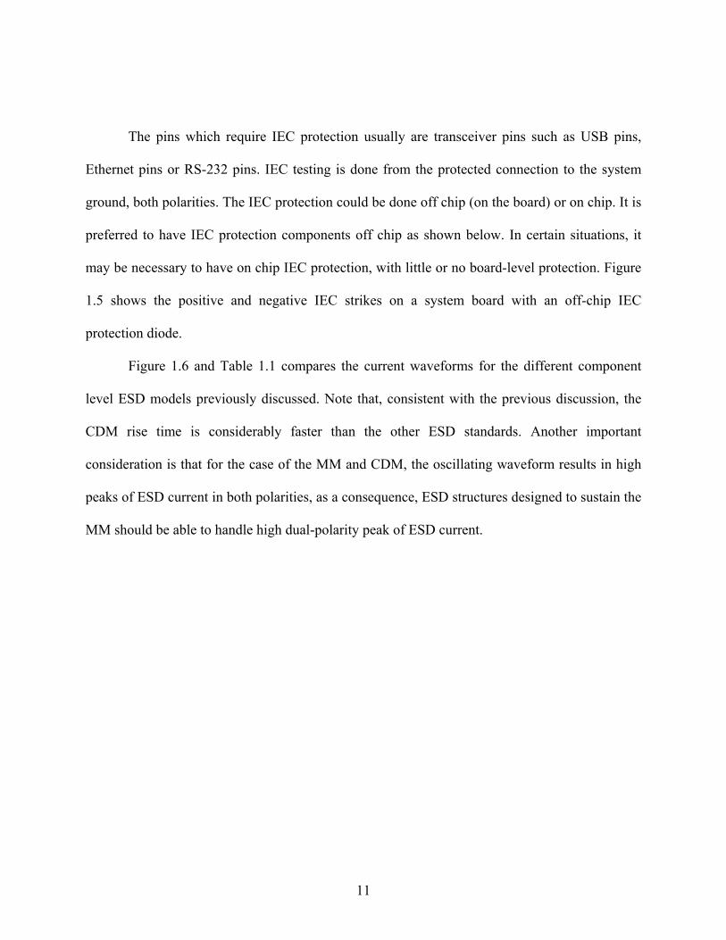
Figure 1.5 The negative (a) and positive (b) IEC zapping on a system board which has a off-chip
IEC protection device. .................................................................................................................. 10
Figure 1.6 Superposed waveforms obtained from the standard component level ESD models.
Waveforms are generated from SPICE simulation....................................................................... 12
Figure 1.7 The VDD-based ESD protection scheme...................................................................... 17
Figure 1.8 The VSS-based ESD protection scheme....................................................................... 17
Figure 1.9 A simplified transient supply clamp, consisting of a capacitor, a resistor and a
MOSFET....................................................................................................................................... 18
Figure 1.10 The ESD design windows for (a) diode-chain-based, and (b) snapback-device-based
supply clamps................................................................................................................................ 20
Figure 2.1 Device cross-section view of the uSCR, showing the locations of the Ln and Lp
regions and the dimensions associated with the device characteristic.......................................... 26
Figure 2.2 The equivalent circuit of the SCR device.................................................................... 30
Figure 2.3 Schematic diagram showing the different cases of Ln+Lp. Lx always keeps at 1μm. . 31

xiii
Figure 2.4 Measured TLP I-V characteristics of the four uSCR devices listed in Table 2.1. ...... 34
Figure 2.5 Measured TLP I-V characteristics of the four uSCR devices listed in Table 2.2. ...... 35
Figure 2.6 (a) Scheme of the on-chip ESD protection realized with the uSCR device. (b)
Equivalent circuit schematic diagram of the layout showed in (a). It shows the discharge current
loops under the different HBM and CDM zaps. ........................................................................... 37
Figure 3.1 The comparison of generic characteristics of the high holding current and the high
holding voltage snapback ESD protection cells within the ESD design window defined by the
supply voltage (VDD), Vmax and the latchup-immune current (ILU). ........................................... 42
Figure 3.2 The device cross-section view of the conventional SCR structure. ............................ 43
Figure 3.3 The equivalent circuit of the SCR device, showing the directions of all electron and
hole current components after the both PNP and NPN transistors turn on................................... 46
Figure 3.4 The top view of the SCR devices. (a) Strip topology of conventional SCR, (b)
segmented topology of high holding current SCR (HHC-SCR), (c) modified HHC-SCR with a
well tie removed from each strip with an interval of every two well ties, and (d) modified HHC-
SCR with a well tie removed from each strip with an interval of every well tie.......................... 47
Figure 3.5 The illustration of the segment topology of the SCR device reported in reference [83].
....................................................................................................................................................... 49
Figure 3.6 TLP measurement results of the conventional SCR, the SCR presented in [83] and
HC-SCR devices with different D3=D4. ...................................................................................... 50
Figure 3.7 TLP measurement results of the HHC-SCR device and the two modified HHC-SCRs
shown in Figure 3.4(c) and (d)...................................................................................................... 51
xiv
Figure 4.1 (a) Cross-section view of the HH-LVTSCR and (b) equivalent circuit of the HH-
LVTSCR. ...................................................................................................................................... 56
Figure 4.2 Schematic of the HH-LVTSCR macromodel with all model elements included,
showing the detailed connections of all internal nodes. ............................................................... 57
Figure 4.3 Different terminal configurations for the parameter extraction of different transistor
models. .......................................................................................................................................... 67
Figure 4.4 Simulated and measured TLP I-V characteristics of the HH-LVTSCR...................... 70
Figure 4.5 (a) Simulated and measured time-dependent pad voltages and (b) simulated and
measured pad currents right after the SCR triggering. ................................................................. 71
Figure 4.6 The simulated pad voltage under VFTLP pulse at a steady-state current of 1A. ........ 71
Figure 4.7 Simulated (a) base-emitter and collector-emitter voltages of the PNP and NPN
transistors and (b) emitter, base and collector currents of the PNP and NPN transistors............. 73
Figure 4.8 Current waveforms of CDM pulses generated by the calibrated CDM equivalent
circuit (insert) with the small target. ............................................................................................. 74
Figure 4.9 (a) Schematic of on-chip ESD protection realized with SCR devices and (b) schematic
showing the discharge current paths of the ESD protection in (a) under the positive and negative
CDM zaps. .................................................................................................................................... 76
Figure 4.10 Simulated transient voltage and current at the input-only pin under a positive 500 V
CDM stress.................................................................................................................................... 78
Figure 4.11 Simulated transient voltage and currents at the output-only pin under a positive 1 kV
CDM stress.................................................................................................................................... 79
Figure 5.1 The model circuit of the SPICE Gummel-Poon bipolar transistor model................... 84
xv
Figure 5.2 (a) The equivalent sub-circuit of VBIC bipolar transistor model and (b) the model
circuit network. ............................................................................................................................. 84
Figure 5.3 (a) Cross-section view of the HH-LVTSCR and (b) equivalent circuit of the HH-
LVTSCR when the macromodel is using VBIC model to describe the NPN transistor............... 86
Figure 5.4 (a) Cross-section view of the HH-LVTSCR and (b) equivalent circuit of the HH-
LVTSCR when the macromodel is using SGP model to describe the NPN transistor................. 86
Figure 5.5 Schematic of the HH-LVTSCR SGP-based macromodel with all model elements
included, showing the detailed connections of all internal nodes................................................. 87
Figure 5.6 Measured and Simulated TLP I-V characteristics of the macromodels built with VBIC
and SGP models............................................................................................................................ 88
Figure 5.7 (a) The measured and simulated time-dependent pad voltages and (b) pad currents by
VBIC-based macromodel right after the SCR triggering. (c) The simulated time-dependent pad
voltages and (d) pad currents by SGP-based macromodel right after the SCR triggering. .......... 89
Figure 5.8 Simulated (a) base-emitter and collector-emitter voltages of the PNP and NPN
transistors and (b) emitter, base and collector currents of the PNP and NPN transistors in the
SGP-based macromodel................................................................................................................ 92
Figure 5.9 The Gummel-Poon plots and output characteristics of VBIC and SGP model of NPN
transistor under normal model extraction conditions.................................................................... 95
Figure 5.10 The Gummel-Poon plot of VBIC and SGP model of NPN transistor when the
macromodels is in conduction mode with a voltage of 10.85 V at Anode. .................................. 97
Figure 5.11 The output characteristics of VBIC and SGP model of NPN transistor when the
macromodels is in conduction mode with a voltage of 10.85 V at Anode. .................................. 98
xvi
LIST OF TABLES
Table 1.1 The comparison of different standard component level ESD models. ......................... 12
Table 2.1 Lateral dimensions and TLP measurement results of the four uSCR devices with
different Ln + Lp. ........................................................................................................................... 33
Table 2.2 Lateral dimensions and TLP measurement results of uSCR-T3 devices with different
D5.................................................................................................................................................. 35
Table 4.1 Comparison of waveforms simulated from the calibrated CDM equivalent circuit in
Figure 4.8 vs. JEDEC specifications............................................................................................. 74
xvii
LIST OF ACRONYMS
ATE Automatic Test Equipment
BiCMOS Bipolar Complementary Metal-Oxide-Semiconductor
BJT Bipolar Junction Transistor
BSIM3v3 Berkeley Short Channel IGFET 3v3
CDM Charged Device Model
DHVSCR Dynamic Holding Voltage Silicon Controlled Rectifier
ESD Electrostatic Discharge
ESDA Electrostatic Discharge Association
HBM Human Body Model
ggNMOS grounded gate N-type MOSFET
HHC-SCR High Holding Current SCR
HH-LVTSCR High-Holding Low-Voltage Triggering SCR
IC-CAP Integrated Circuit Characterization and Analysis Program
ICs Integrated Circuits
IEC International Electrotechnical Commission
JEDEC Joint Electron Device Engineering Council
LIGCSCR Latch-Up-Immune Gate-Coupled LVTCSR
LOCOS Local Oxidation of Silicon
LVTSCR Low-Voltage Triggering SCR

xviii
MLSCR Modified Lateral SCR
MM Machine Model
MOS Metal Oxide Semiconductor
MOSFET MOS Field Effect Transistor
NESD N-type ESD
PLDD P-type Lightly-Doped Drain
RF Radio Frequency
SCR Silicon Controlled Rectifier
SGP SPICE Gummel-Poon
SPDT Single Pole Double Throw
SPICE Simulation Program with Integrated Circuit Emphasis
TCAD Technology Computer Aided Design
TDDB Time-Dependent Dielectric Breakdown
TLP Transmission Line Pulse
uSCR un-Assisted Low-Trigger and High Holding Voltage SCR
VFTLP Very-Fast TLP
VBIC Vertical Bipolar Inter-Company

1
CHAPTER 1. INTRODUCTION
1.1. What is ESD
Electrostatics, or static electricity, is an excess of deficiency of electrons on a surface. It
is as old as the time itself. Static electricity is caused by contact and separation of 2 dissimilar
materials including solids, liquids and gas. The very first documented observation of static
electricity generation is back to 600 B.C. when Greeks rubbed amber with a piece of fur and
observed attraction of lightweight objects to the amber. Electrostatic discharge (ESD) is the
transfer of electrons between two bodies at different static potentials. The three mechanisms
being responsible for generating the potential difference are triboelectrification, induction and
conduction. The famous experiment is Franklin’s kite test in 1952 showing lightening is an ESD
event [1].
Back to our everyday’s life, no one could hardly experience some kind of ESD events,
like experiencing the shocking sparks when touching a door handle of a car. The damages caused
by ESD should never been overlooked.
1.2. How is ESD Relevant to Semiconductor Industry
The ESD problem became a real issue after World War II as highly insulating polymeric
materials found widespread usage where substantial static charge accumulation might cause
machinery shut downs. However, the devastating ESD damage problem was not taken into
serious consideration until the modern microelectronics technologies took the role in our
2
everyday life, which is how ESD failure problem became relevant to semiconductor integrated
circuits (ICs) technologies [1]-[3].
Only a half century after the development of ICs was initiated, ICs have become
ubiquitous. Modern computing, communications, manufacturing and transport systems,
including Internet, all depend on the existence of integrated circuits. Technological innovation in
the semiconductor industry has never slowed down. The evolution in the downscaling of the
physical dimensions is considered a main factor in obtaining lower cost, while achieving better
performance and more compact ICs, all of them keys for today’s demanding applications [4].
ESD failure is a profound reliability problem to ICs and poses a grand challenge to the
semiconductor industry [5]. The impact of the invisible ESD phenomena became materialized
with the invention of semiconductor transistor in 1947 and the development of metal-oxide
semiconductor (MOS) technologies in the 1960s. The electronic device and system failures due
to ESD events in the semiconductor industry escalated almost exponentially in the 1970s [1]. As
the semiconductor ICs technologies keep on downscaling, ICs parts become increasingly
susceptible to ESD damages [6]-[9]. Statistics indicated that up to 30% of all ICs failure might
be attributed to ESD [10]. The actual cost of ESD damage to the electronics industry is running
into the billions of dollars annually [11]. And ESD protection has become a topic of major
interest and discussion [12]-[14].
1.3. ESD Failure Modes on ICs and ESD models
ESD damage to electronic devices can occur at any point from manufacture to field
service. Damage results from handling the devices in uncontrolled surroundings or when poor

3
ESD control practices are used. Generally damage is classified as either a catastrophic failure or
a latent defect.
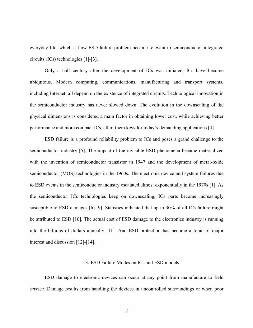
The catastrophic failure causes immediate ICs malfunction. There are mainly three failure
modes for permanently damaging semiconductor devices due to ESD events [15]-[16] and they
can be described as followings:
1. Oxide failure: oxide may have void formation, vaporization and filament
formation, leading to shorts or opens [17], as shown in Figure 1.1(a).
2. Metallization burnout: metal and contacts may melt and vaporization may
occur, leading to shorts and opens, as shown in Figure 1.1(b).
3. Junction damage or burnout: junction may melt and cross diffusion or lattice
damage may occur. It is an important mechanism in bipolar junction transistor
[18] and MOS devices [19]. In NMOS, this failure is often displayed by a high
reverse leakage current, and it may be due to a redistribution of n-type dopants
into the channel or due to lattice damage during the ESD event, as shown in
Figure 1.1(c).
A latent defect is more difficult to identify. A device that is exposed to an ESD event may
be partially degraded, yet continue to perform its intended function. However, the operating life
of the device may be reduced dramatically. A product or system incorporating devices with
latent defects may experience premature failure after the user places them in service. Such
failures are usually costly to repair and in some applications may create personnel hazards.
4
Figure 1.1 Illustrations of the three basic failure mechanisms: (a) oxide failure, (b) metallization burnout, and (c) junction damage or burnout.
ESD damage is usually caused by one of three events: direct electrostatic discharge to the
device, electrostatic discharge from the device or field-induced discharges. Damage to an ESD
sensitive device by the ESD event is determined by the device’s ability to dissipate the energy of
the discharge or withstand the voltage levels involved. This is known as the device’s ESD
sensitivity.
Discharge to the device. An ESD event can occur when any charged conductor (including
the human body) discharges to an ESD sensitive device. The most common cause of electrostatic
(a)
(b) (c)
5
damage is the direct transfer of electrostatic charge from the human body or a charged material
to the electrostatic discharge sensitive device. When one walks across a floor, an electrostatic
charge accumulates on the body. Simple contact of a finger to the leads of a device or assembly
allows the body to discharge, possibly causing device damages. The model used to simulate this
event is the Human Body Model (HBM). A similar discharge can occur from a charged
conductive object, such as a metallic tool or fixture. The model used to characterize this event is
known as the Machine Model (MM).
Discharge from the device. The transfer of charge from an ESD sensitive device is also
an ESD event. Static charge may accumulate on the ESD sensitive device itself through handling
or contact with packaging materials, work surfaces, or machine surfaces. This frequently occurs
when a device moves across a surface or vibrates in a package. The model used to simulate the
transfer of charge from an ESD sensitive device is referred to as the Charged Device Model
(CDM). The capacitance and energies involved are different from those of a discharge to the
ESD sensitive device. In some cases, a CDM event can be more destructive than the HBM for
some devices.
The trend towards automated assembly would seem to solve the problems of HBM ESD
events. However, it has been shown that components may be more sensitive to damage when
assembled by automated equipment. A device may become charged, for example, from sliding
down the feeder. If it then contacts the insertion head or another conductive surface, a rapid
discharge occurs from the device to the metal object.
Field induced Discharges. Another event that can directly or indirectly damage devices is
termed Field Induction. As noted earlier, whenever any object becomes electrostatically charged,
6
there is an electrostatic field associated with that charge. If an ESDS device is placed in that
electrostatic field, a charge may be induced on the device. If the device is then momentarily
grounded while within the electrostatic field, a transfer of charge from the device occurs as a
CDM event. If the device is removed from the region of the electrostatic field and grounded
again, a second CDM event will occur as charge (of opposite polarity from the first event) is
transferred from the device.
1.4. Characterization of ESD performance in ICs
Based on the three ESD damage events mentioned above, standard ESD models which
simulate real ESD events have been constituted by ESD Association (ESDA) and Joint Electron
Device Engineering Council (JEDEC) in order to characterize the susceptibility of an IC to ESD
damage. ICs will be tested by stressing the device under test (DUT) with emulated ESD zaps of
different models, a procedure called ESD zapping. The ESD models are represented as lumped
circuit equivalents, so that testing is consistent and reliability can be defined as a quantitative
attribute.
1.4.1. Human Body Model (HBM)
The HBM is intended to represent the electrostatic discharge from the fingertip of a pre-
charged human being delivered to a device [20]-[21]. The discharge current levels can be 1-4 A
with a rise time of 10 ns and a discharge time constant of 150 ns. The HBM lumped circuit
model is represented as a capacitor discharging through a resistor, with the capacitance CESD =
7
100 pF, the inductance LESD ≈7.5 μH, and the resistance RESD = 1.5 k ohm, as shown in Figure
1.2.
DUTVESD
CESD=100pF+-
LESD=7.5
S
RESD=1500Short
R=500
Load for waveform calibration
μHΩ
ΩDUTVESD
CESD=100pF+-
LESD=7.5
S
RESD=1500Short
R=500
Load for waveform calibration
μHΩ
Ω
Figure 1.2 The simplified lumped circuit representation for ESD HBM model.
1.4.2. Machine Model (MM)
The MM is intended to represent the interaction of electrical discharge from a pre-
charged conductive source, such as metallic tools or machine, to the component [22]-[23]. In
Japan, this model is widely used in the automotive industry. The standardized waveform for the
MM is obtained by the lumped circuit as in Figure 1.3, the capacitor CESD = 200 pF, the inductor
LESD ≈1.5 μH, and the resistance RESD < 1 Ω. With essentially no series resistance in its path,
the MM event has higher current levels than the HBM for the same charging voltage. The MM is
a damped sinusoidal oscillating current waveform, and the time to the first current peak is
typically 15ns with duration for the pulse of approximately 40ns. Although the pulse width
appears to be less, the power dissipation in the IC is dominated by the time at the peak current
level, and this is nearly the same for both HBM and MM. Hence, the failure currents for HBM
8
and MM will be approximately the same and the equivalent MM level to a 2000V HBM under
the present ESD Association Standards is about 100V with a peak current of 1.7A.
DUTVESD
CESD=200pF+-
LESD=1.5
S
RESD< 1Short
R=500
Load for waveform calibration
μHΩ
ΩDUTVESD
CESD=200pF+-
LESD=1.5
S
RESD< 1Short
R=500
Load for waveform calibration
μHΩ
Ω
Figure 1.3 The simplified lumped circuit representation for ESD MM model.
1.4.3. Charged Device Model (CDM)
The CDM represents the electrostatic discharge occurring from a chip via an external
grounded element. Different from HBM and MM, in the CDM event it is the packaged integrated
circuit that accumulates the charge on its package and/or die [24]-[25]. During a CDM event
rapid discharge occurs with the resulting current levels in tens of amperes and very fast rise time
(<500ps rise time). The resulting damage due to such direct pin discharge is normally gate oxide
breakdown. Because of the widespread use of automated manufacturing and testing line, as well
as thinner and thinner gate oxides in advanced technologies, the CDM model has gained
importance in more recent years [26]-[27]. CDM levels are dependent on package type and
hence the same protection scheme may give different levels from one product chip to another
product chip. Note that while the ratio for HBM and MM equivalence is more than 20:1, i.e. a
100V MM threshold is the same as a 2000V HBM threshold, CDM thresholds are not directly
9
linked to HBM and MM thresholds. A typical CDM setup is shown in Figure 1.4, where the ESD
sensitive DUT is placed upside down on a charge plate, charged by a high voltage source, and
then discharge through a discharge head. There are two different means for charging up the DUT:
direct charging and field induced charging. The former charges the DUT by direct contact. The
latter, recommended by many test standards, charges the DUT through electric field induction.
The CDM is the fastest of the ESD phenomena, and the equivalent lumped circuit typically
includes, a capacitor CESD = 6.8 pF, an inductor LESD <1 μH, and the resistance RESD = 1 ohm.
VESD
CESD=6.8pF
RESD=1Ω
DUT
V
LESD<1µH
VESD
CESD=6.8pF
RESD=1Ω
DUT
V
LESD<1µH
Figure 1.4 Simplified CDM lumped circuit representation.
1.4.4. System-Level ESD Standard IEC 61000-4-2
IEC stands for International Electrotechnical Commission. IEC 61000-4-2 is a widely
accepted European standard which defines a system level ESD event that is meant to be tested on
actual end equipments like PCs, PDAs, set top boxes, etc. In this standard two different test
procedures are defined, the air-gap test and the contact test. Commonly, the air-gap test is less
10
repeatable than the contact test. In regular testing programs, circuits are tested powered up and
powered down in order to guarantee functionality after stress, not only when the system is off but
also during operation. This IEC standard defines an ESD event that is much stronger than a
component level ESD event such as HBM, CDM. For instance, a level 4 IEC 61000-4-2 ESD
event has a peak current of 30A, compared to a 2kV HBM peak current of 1.3 A.
- IEC strike
System GND
Port to be protected
+ IEC strike
Chip
Chip
Board
Board
ESD Clamp
System GND
Port to be protected
ESD Clamp
On-Chip ESD Protection
Off-Chip IEC Protection Diode
On-Chip ESD Protection
Off-Chip IEC Protection Diode
(a)
(b)
- IEC strike
System GND
Port to be protected
+ IEC strike
Chip
Chip
Board
Board
ESD Clamp
System GND
Port to be protected
ESD Clamp
On-Chip ESD Protection
Off-Chip IEC Protection Diode
On-Chip ESD Protection
Off-Chip IEC Protection Diode
(a)
(b)
Figure 1.5 The negative (a) and positive (b) IEC zapping on a system board which has a off-chip IEC protection device.
11
The pins which require IEC protection usually are transceiver pins such as USB pins,
Ethernet pins or RS-232 pins. IEC testing is done from the protected connection to the system
ground, both polarities. The IEC protection could be done off chip (on the board) or on chip. It is
preferred to have IEC protection components off chip as shown below. In certain situations, it
may be necessary to have on chip IEC protection, with little or no board-level protection. Figure
1.5 shows the positive and negative IEC strikes on a system board with an off-chip IEC
protection diode.
Figure 1.6 and Table 1.1 compares the current waveforms for the different component
level ESD models previously discussed. Note that, consistent with the previous discussion, the
CDM rise time is considerably faster than the other ESD standards. Another important
consideration is that for the case of the MM and CDM, the oscillating waveform results in high
peaks of ESD current in both polarities, as a consequence, ESD structures designed to sustain the
MM should be able to handle high dual-polarity peak of ESD current.

12
0 20 40 60 80 100 120
-4
-2
0
2
4
6
8
10
121kV CDM
through Small Target
200V MM
2 kV HBMCur
rent
(A)
Time (ns)
2kV HBM 200V MM 1kV CDM through Small Target
Figure 1.6 Superposed waveforms obtained from the standard component level ESD models. Waveforms are generated from SPICE simulation.
Table 1.1 The comparison of different standard component level ESD models.
Model HBM MM CDM Voltage Level 2 kV 200V 1 kV through small target Pulse Width ~ 150 ns ~ 40 ns ~ 1 ns Rise Time 2 ~ 10 ns 10 ~ 15 ns 100 ~ 500 ps
Peak Current 1.33 A ~3.6 A 12 A
1.4.5. Transmission Line Pulse (TLP)
All the existing ESD test models, as discussed above, share one common
disadvantageous feature that the ESD test methods developed upon them are destructive. Such
ESD zapping tests provide results about ESD failure threshold of an ESD sensitive device.
13
However, they offer no insights into the possible failure mechanisms, which are critical to ESD
protection design. Such information can be obtained by use of a transmission line pulse (TLP)
technique. TLP technique has been increasingly accepted in practical ESD protection circuit
design since it was introduced into ESD protection design [29]. Many TLP testing systems with
different flavor exist [12], [30]. The principle for TLP test is that a piece of transmission line
cable is charged by a voltage source, and the TLP system forces a trapezoidal current waveform
into device under test, easier to control compared to that generated based on other ESD test
standards [30]-[31]. The pulse width of the TLP is a function of the length of the transmission
line and the propagation velocity of the transmission line. For this method, the standard choice of
pulse width has been determined based on the HBM model, i.e., the TLP current level gives an
estimated HBM level [30], [32]. This ESD characterization method allows for a closer estimation
of the device conducting characteristics. It also provides an idea of the quasi-static behavior of
the ESD device since reliable data can be taken during the 100 ns time frame of the pulse width,
with having reduced effects of self-heating in the device. In this respect, the TLP curve below the
second-breakdown point can be considered a good approach to a dc-simulated curve. However, it
still represents the way the device responds to ESD stress because it reveals the operating points
after the initial turn-on transient.
1.5. Commonly Used ESD On-Chip Protection Circuits
There are two general methods to reduce IC failure due to ESD. One consists of the usage
of ionization apparatus, the proper handling and grounding of personnel and equipment during
manufacturing, and the usage of safety packaged chips, i.e., to prevent ESD events from
14
occurring [33]. The other method is to incorporate effective on-chip protection circuitry inside
ICs, which would shunt high currents to keep ESD strikes away from the internal circuitry and
clamp high voltages during an ESD event [34]-[35]. A chip manufacturer has partial control over
a customer’s handling of its product, but it is not possible to guarantee total ESD immunity.
However, through the proper design of on-chip protection structures, the threshold of sustainable
stress can be significantly increased, resulting in improved reliability of the ICs and electronics
systems [12]-[14], [17].
1.5.1. The Qualities of Good ESD Protection
The capability of ESD protection circuitry can be determined by its performance in four
categories: robustness, effectiveness, speed and transparency. Good ESD protection must
function well in all of these areas [12].
Robustness – Robustness describes the ability of the ESD protection circuitry to handle
the ESD current by itself. It is defined as the ESD level at which the ESD protection circuitry
fails. For example, a protection circuitry that can withstand a peak current of 3 A on the HBM
timescale has a robustness of 4.5 kV HBM. Robustness is usually, but not always, proportional
to the width of the protection circuitry. Therefore, it is often convenient to measure the
breakdown characteristics of a protection device with TLP or HBM testing and quantify its
failure level in milliamperes per micrometer or HBM volts per micrometer.
Effectiveness – Effectiveness describes the ability of the protection circuitry to limit the
voltage to a safe level such that circuits in parallel with the ESD protection do not fail. To
15
achieve higher protection levels, the voltage sustained across the ESD protection circuitry must
decrease or the turn-on voltage of the failing elements must increase.
Speed – Speed is of particular importance for CDM events, with their subnanosecond rise
time. Even robust and effective ESD networks must activate with enough speed to clamp the
ESD event at a safe level without causing circuits in parallel to fail.
Transparency – Transparency requires that the ESD protection not interfere with the
normal operation of the I/O circuit and of the chip itself. This includes the ESD clamp should not
have so much capacitance that it violates the loading limits of the I/O signaling specification, the
ESD clamp must not draw excessive current at either high or low input or output levels, the ESD
clamp must be compatible with the normal sequence for applying power, and the ESD clamp has
to be able to tolerate the over-voltage conditions.
1.5.2. ESD Protection Schemes
In ESD measurement practice of HBM and MM, ESD pulses zap through 2 pin
combinations in different directions, i.e., zapping the I/O pin versus the power supply pin in both
polarities, zapping the I/O pad to the ground pin in both polarities, zapping the I/O pin versus I/O
pin in both polarities and zapping power supply pin versus ground pin in both polarities [20]-[23].
For the case of CDM, the whole component package will be charged positively and negatively
then all pins will be grounded respectively. The discharge current will go into or come out of the
package from the grounded pin to the substrate of the chip [24]-[25]. A good ESD protection
network must provide a discharge path for all pin combinations and must limit the voltage across
any sensitive devices. Most ESD solutions rely on shunting charge from an I/O pin to a power
16
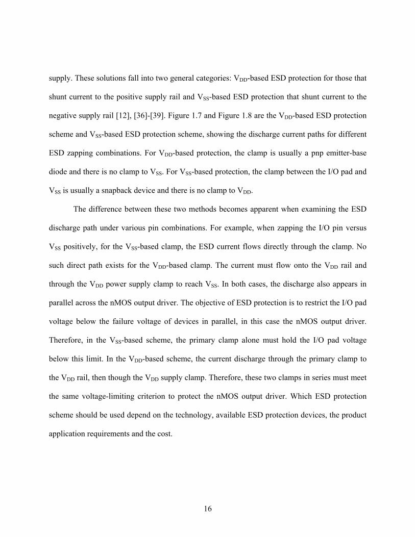
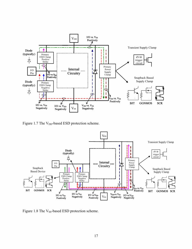
supply. These solutions fall into two general categories: VDD-based ESD protection for those that
shunt current to the positive supply rail and VSS-based ESD protection that shunt current to the
negative supply rail [12], [36]-[39]. Figure 1.7 and Figure 1.8 are the VDD-based ESD protection
scheme and VSS-based ESD protection scheme, showing the discharge current paths for different
ESD zapping combinations. For VDD-based protection, the clamp is usually a pnp emitter-base
diode and there is no clamp to VSS. For VSS-based protection, the clamp between the I/O pad and
VSS is usually a snapback device and there is no clamp to VDD.
The difference between these two methods becomes apparent when examining the ESD
discharge path under various pin combinations. For example, when zapping the I/O pin versus
VSS positively, for the VSS-based clamp, the ESD current flows directly through the clamp. No
such direct path exists for the VDD-based clamp. The current must flow onto the VDD rail and
through the VDD power supply clamp to reach VSS. In both cases, the discharge also appears in
parallel across the nMOS output driver. The objective of ESD protection is to restrict the I/O pad
voltage below the failure voltage of devices in parallel, in this case the nMOS output driver.
Therefore, in the VSS-based scheme, the primary clamp alone must hold the I/O pad voltage
below this limit. In the VDD-based scheme, the current discharge through the primary clamp to
the VDD rail, then though the VDD supply clamp. Therefore, these two clamps in series must meet
the same voltage-limiting criterion to protect the nMOS output driver. Which ESD protection
scheme should be used depend on the technology, available ESD protection devices, the product
application requirements and the cost.
17
Internal Circuitry
I/O Pin
VDD
VSSI/O vs. VDDNegatively
Primary ESD Clamp
Negative Strike
Primary ESD Clamp
Positive Strike
PrimaryPower SupplyClamp
I/O vs. VSSNegatively
I/O vs. VSSPositively
VDD vs. VSSNegatively
VDD vs. VSSPositively
Snapback Based Supply ClampDiode
(typically)
Diode(typically)
BJT GGNMOS SCR
Transient Supply Clamp
dV/dttrigger circuit
I/O vs . VDDPositively
Internal Circuitry
I/O Pin
VDD
VSSI/O vs. VDDNegatively
Primary ESD Clamp
Negative Strike
Primary ESD Clamp
Positive Strike
PrimaryPower SupplyClamp
I/O vs. VSSNegatively
I/O vs. VSSPositively
VDD vs. VSSNegatively
VDD vs. VSSPositively
Snapback Based Supply ClampDiode
(typically)
Diode(typically)
BJT GGNMOS SCR
Transient Supply Clamp
dV/dttrigger circuit
I/O vs . VDDPositively I/O vs . VDDPositively
Figure 1.7 The VDD-based ESD protection scheme.
Internal Circuitry
I/O Pin
VDD
VSSI/O vs. VDDNegatively
I/O vs. VSSNegatively I/O vs. VDD
Positively I/O vs. VSSPositively
VDDvs. VSSNegatively
VDD vs. VSSPositively
Snapback Based Supply Clamp
Diode(typically)
BJT GGNMOS SCR
Transient Supply Clamp
dV/dttrigger circuit
Primary ESD ClampPositive
Strike
Primary ESD Clamp
Negative Strike
PrimaryPower Supply ClampSnapback
Based Device
BJT GGNMOS SCR
Figure 1.8 The VSS-based ESD protection scheme.

18
1.5.3. Power Supply Clamp Design
For both ESD protection scheme, they all have primary power supply clamp. There are
two types of supply clamp, the static supply clamp and the transient supply clamp. Transient
supply clamp has been used widely in preventing ESD damage [40]-[41]. It has been proven to
offer robust, scalable, portable and easily simulated [42]-[48]. The operation of transient clamps
depends on both a trigger voltage and the rate at which that voltage is applied (dV/dt). Figure 1.9
shows a simple transient supply clamp circuit, which consists of a capacitor, a resistor and a
MOS device, to illustrate basic concept of how the transient clamp works. When the microchip
(i.e., circuit core) being protected is subjected to the ESD stress, the ESD pulse will be fed
simultaneously to the external capacitor C and drain terminal of the MOSFET in the ESD
protection circuit. Such a pulse, which has a very high voltage, will give rise to a voltage drop in
the external resistor R and therefore will turn on the MOSFET within a very short period of time.
A lot of transient supply clamp designs have been presented in literatures [42]-[48].
C
R
SUPPLY
VSS
Control Node
Transient Power Supply Clamp
C
R
SUPPLY
VSS
Control Node
Transient Power Supply Clamp
Figure 1.9 A simplified transient supply clamp, consisting of a capacitor, a resistor and a MOSFET.
19
In additional to the transient supply clamp, the static supply clamps are also being used
widely. The static supply clamp can be diode chain which is only applicable for low voltage
supplies or snapback-based devices (as shown in Figure 1.7 and Figure 1.8). The static supply
clamp is designed to respond when a specific trigger voltage is exceeded. To realize the effective
ESD protection without interfering with the normal operation of the protected circuit, the key
considerations include (as shown in Figure 1.10): 1) the turn-on voltage or the trigger voltage
(VT) and the clamping voltage at the required ESD protection level have to be kept below the
voltage of internal circuitry breakdown, 2) the sustain point (also called holding point) in the
case of the snapback devices has to be larger than the power supply voltage (VDD) to avoid
latchup problems [49], 3) low leakage current at operating voltage DVD, 4) good robustness, i.e.,
high second breakdown current (It2) per unit area. In additional, for the static supply clamp using
snapback-based device, if its clamped voltage is low enough and the robustness is high enough in
reverse operation, the extra diode between supply and VSS in supply ESD protection section (in
Figure 1.7 and Figure 1.8) and the primary ESD clamp for negative strikes in signal ESD
protection section (in Figure 1.8) can be removed to save area.
20
Figure 1.10 The ESD design windows for (a) diode-chain-based, and (b) snapback-device-based supply clamps.
Normally, there are three type of devices, bipolar junction transistor (BJT), MOS field –
effect transistor (MOSFET) and silicon controlled rectifier (SCR) having been used to form the
snapback-based power supply clamp and the primary ESD clamp for positive strikes, as shown
ESD Design Window
Nor
mal
Ope
ratio
n
Inte
rnal
Circ
uitry
Bre
akdo
wn
VT
IT2
VDD Vmax
Ron
Voltage
Cur
rent
ESD Design Window
Nor
mal
Ope
ratio
n
Inte
rnal
Circ
uitry
Bre
akdo
wn
VT IT
IH
IT2
VH
VDD Vmax
Ron
Voltage
Cur
rent
(a)
(b)
21
in Figure 1.7 and Figure 1.8. A BJT is actually the underlying building bricks of these advanced
ESD protection networks. When BJT is used in ESD protection, [39], [50]-[51], the collector of
the BJT is normally connected to the protected pad, the emitter to one of the power rails, and an
additional resistor between the base and emitter is incorporated. When the ESD pulse appears in
the protected pad, the BJT can go into the snapback mode and create a low impedance discharge
path that guarantees the integrity of the protected circuit.
Another proven protection element more often used in CMOS technologies is the
MOSFET. For example, the grounded gate N-MOSFET (ggNMOS) with minimum design
channel length and gate-, source-, and bulk- contacts tied together to ground represents the key
element of many ESD protection concepts. Beside its electrical properties, it is available at the
beginning of the technology definition, characterized at the early stages of the development
process, as well as area-effective.
The operation of the ggNMOS during an ESD event is mainly controlled by the
embedded NPN BJT, formed by the drain (n+), bulk (p), and source (n+), lateral structure [12].
As a result, the ggNMOS goes into snapback [52] during an ESD event and can be often self-
protected. A similar concept applies to the PMOS. A lot of design works have been done to use
MOS device as ESD protection [53], for example, PNP-driven NMOS [53], substrate triggered
NMOS [54], NMOS triggered NMOS [55], etc. A drawback of an ESD device with MOS gate is
that it can suffer long-term reliability problems if the pad operating voltage is higher than the
pre-established voltage rating, or if a relatively large electric field is applied at the gate during
the ESD event [56].

22
Different SCR-based device designed for ESD protection have been proposed in the
literature using an experimental approach [57]. The SCR-based devices are not standard
structures optimized in CMOS or Bipolar Complementary Metal-Oxide-Semiconductor
(BiCMOS) processes, and even though these devices can be the most efficient structures in terms
of ESD protection, it has been rather difficult to design functional SCR-based protection devices
[58] and effective compact modeling techniques for this type of device are also required.
Although the SCR-type structures might serve as superior ESD protection components in
CMOS/BiCMOS technologies, the embedded SCR in the CMOS/BiCMOS processes has been,
instead, a cause of concern because of the latchup problem [49], [60]. Thus, the challenge in the
ESD design using SCR-based structures is to maintain a safe operation in the circuit without a
latchup problem, while obtaining the advantage of the deep snapback and high conductivity
modulation for high ratio of ESD protection per unit area [59].
1.6. Dissertation Outline
The investigation presented in this dissertation provides a comprehensive study of the
design, characterization and integration of the ESD protection using SCR-based structures and
the development and implementation of compact models for the SCR-based structures to predict
ESD protection level and evaluate the interaction of ESD cell with core circuitry at pre-silicon
stage. The organization of the dissertation is as following.
Chapter 2 starts with design methodologies followed by presenting the design of a novel
and robust un-assisted low-trigger and high holding voltage SCR (uSCR) for low voltage
application and the implementation of such device into whole chips to realize optimized ESD

23
protection. Chapter 3 addresses a new high holding current SCR (HHC-SCR) for the ESD
protection of high voltage applications. Chapter 4 describes the development of a simulation
program with integrated circuit emphasis (SPICE) equivalent-circuit model for the SCR used for
ESD protection applications, with emphasis being placed on the simulation of circuits subject to
an fast-transient and highly destructive ESD event known as CDM. The framework developed
includes the equivalent circuit, model components’ equations, and model parameter extraction.
Chapter 5 assesses two SCR macromodels by using Vertical Bipolar Inter-Company (VBIC)
model and SPICE Gummel-Poon (SGP) model respectively are presented and the simulations
results of both macromodels are compared with measurements. Comparing with SGP model, the
unique advanced features of VBIC model for building an accurate SCR macromodel have been
pointed out and analyzed from device physics and model theory perspectives. Chapter 6 comes
summary and conclusion of the dissertation.
24
CHAPTER 2. DESIGN AND INTEGRATION OF LOW VOLTAGE ESD PROTECTION DEVICES FOR AREA-EFFICIENT ON-CHIP ESD
PROTECTION
2.1. Introduction
As processes are scaling down, the breakdown voltage of internal circuitry is lower and
lower. Especially for the ultra-thin gate oxide, with the time-dependent dielectric breakdown
(TDDB) continually decreasing. To cover both intrinsic and extrinsic gate oxide failure, the
suggested maximum permissible voltage limit under Electrostatic Discharge (ESD) conditions is
10 V for deep submicron process and below [61]. When using the VSS-based ESD protection
scheme as shown in Figure 1.8, the trigger voltage of designed snapback-based ESD protection
cells, which are sitting as the primary ESD clamp for positive strikes on I/O pad in Figure 1.8
and as the primary power supply clamp between supply and VSS in Figure 1.7 and Figure 1.8,
should be lower than 10V. For a 3.3 V product application running on the feature size of 0.35 μm,
taking into account the maximum transient voltage, the holding voltage of the ESD protection
cells should be higher than 5 V and/or the holding current of ESD cell should be higher than the
minimum latch-up current in order to avoid a latch-up issue [49]. Such a narrow ESD design
window (refer to Figure 1.10) presents a big challenge to the device/circuit engineers.
SCRs also known as thyristors are used extensively in power device applications because
of the capability to switch from very high impedance state to a very low impedance state. Such
device has long been used as an on-chip ESD protection element to form snapback-based ESD
clamp [62]-[63] over a broad rang of technologies because of its low on-resistance, high failure
25
current and the best area efficiency for on-chip ESD protection [12], [62]-[64], but a
conventional SCR’s trigger voltage is higher than 10 V and the transient-induced latch-up is still
a major problem. Some SCR devices have been reported to have a low switching voltage, such as
gate-coupled low-voltage triggering (LVTSCR) [65], grounded-gate NMOS triggered SCR [61],
double-triggered SCR [66], smart triggered multi-finger SCR [67], etc., but those SCR devices
have to be assisted by external trigger circuitry to reach such low trigger voltage. For latch-up,
two methods were reported to solve this problem. One way is to increase the trigger current [68]
or by increasing the holding current [69]. The former has to use trigger circuitry to insure low
trigger voltage and the latter needs to shunt an external resistance and gate structure, which
consume the layout area. Besides these, the highly latch-up-immune gate-coupled LVTCSR
(LIGCSCR) [70] was also reported, but the properly designed control circuits need to be
involved. In addition, the holding voltage of dynamic holding voltage SCR (DHVSCR) [71] has
been shown to be not high enough.
This chapter presents the first un-assisted, low-trigger and high-holding voltage SCR
(uSCR), which can simultaneously realize a trigger voltage as low as 7 V and a tunable holding
voltage from 5 to 7.5 V without using any external circuitry [72]-[74]. The ESD robustness of
the uSCR in both positive and negative operations are higher than 60 mA/μm, thus enabling
excellent ESD protection levels of +/- 8 kV HBM and +/- 2 kV CDM based on JEDEC standard,
when using uSCR as the primary ESD clamp for positive strikes on I/O pad and as the primary
supply clamp between supply and VSS in the ESD protection scheme of Figure 1.8.
26
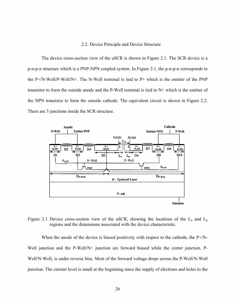
2.2. Device Principle and Device Structure
The device cross-section view of the uSCR is shown in Figure 2.1. The SCR device is a
p-n-p-n structure which is a PNP-NPN coupled system. In Figure 2.1, the p-n-p-n corresponds to
the P+/N-Well/P-Well/N+. The N-Well terminal is tied to P+ which is the emitter of the PNP
transistor to form the outside anode and the P-Well terminal is tied to N+ which is the emitter of
the NPN transistor to form the outside cathode. The equivalent circuit is shown in Figure 2.2.
There are 3 junctions inside the SCR structure.
N +N + P +
P- sub
N - Epytaxial Layer
P +
N-Well Emitter-PNP Emitter-NPN P-WellAnode Cathode
D1
D2
D3
D4
D5 D8
D9
D10
Lx
D7
DN-Well DP-Well
Substrate
Ln Lp
NESD PLDDNLDD PLDDN +
NLDDP +
PLDD
Rp-wellNPNPNP
P- WellN- WellD6
Rn-well
PLDDNESD
N +N + P +
P- sub
N - Epytaxial Layer
P +
N-Well Emitter-PNP Emitter-NPN P-WellAnode Cathode
D1
D2
D3
D4
D5 D8
D9
D10
Lx
D7
DN-Well DP-Well
Substrate
Ln Lp
NESD PLDDNLDD PLDDN +
NLDDP +
PLDD
R
N +N + P +
P- sub
N - Epytaxial Layer
P +
N-Well Emitter-PNP Emitter-NPN P-WellAnode Cathode
D1
D2
D3
D4
D5 D8
D9
D10
Lx
D7
DN-Well DP-Well
Substrate
Ln Lp
NESD PLDDNLDD PLDDN +
NLDDP +
PLDD
Rp-wellNPNPNP
P- WellN- WellD6
Rn-well
PLDDNESD
Figure 2.1 Device cross-section view of the uSCR, showing the locations of the Ln and Lp regions and the dimensions associated with the device characteristic.
When the anode of the device is biased positively with respect to the cathode, the P+/N-
Well junction and the P-Well/N+ junction are forward biased while the center junction, P-
Well/N-Well, is under reverse bias. Most of the forward voltage drops across the P-Well/N-Well
junction. The current level is small at the beginning since the supply of electrons and holes to the
27
center junction is restricted by the reverse-biased junction on either side [75]. If holes are
injected from P+ to N-Well and will recombine with electrons in N-Well region to maintain
space charge neutrality, the supply of electrons in current situation is severely restricted since N-
Well region is terminated in the reverse-biased P-Well/N-Well junction. It is the same thing to
electrons injected from N+ to P-Well region. The P-Well/N-Well junction is the blocking
junction. The supply of electrons and holes are from the thermal generation of electron-hole pairs
at the center junction. As a result, the total current is approximately the reverse saturation current
of the center junction and the SCR device is in forward-blocking state. The reverse saturation
current passing through the center junction will be multiplied by the carrier multiplication due to
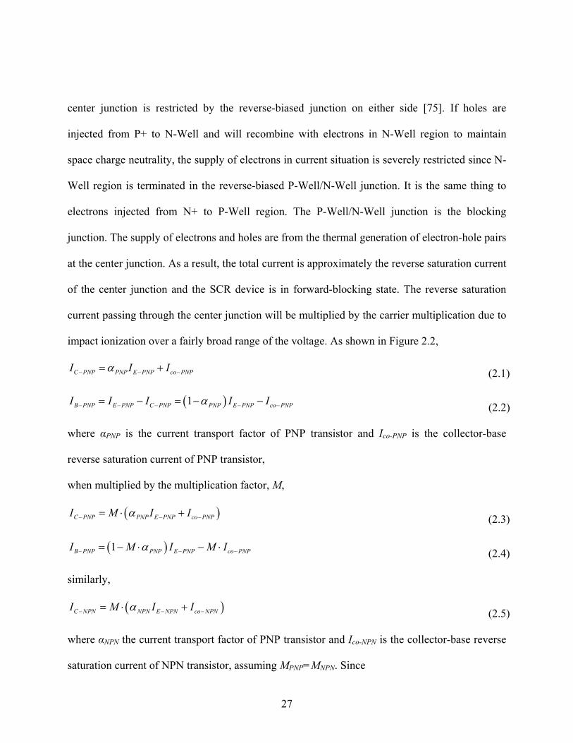
impact ionization over a fairly broad range of the voltage. As shown in Figure 2.2,
C PNP PNP E PNP co PNPI I Iα− − −= + (2.1)
( )1B PNP E PNP C PNP PNP E PNP co PNPI I I I Iα− − − − −= − = − − (2.2)
where αPNP is the current transport factor of PNP transistor and Ico-PNP is the collector-base
reverse saturation current of PNP transistor,
when multiplied by the multiplication factor, M,
( )C PNP PNP E PNP co PNPI M I Iα− − −= ⋅ + (2.3)
( )1B PNP PNP E PNP co PNPI M I M Iα− − −= − ⋅ − ⋅ (2.4)
similarly,
( )C NPN NPN E NPN co NPNI M I Iα− − −= ⋅ + (2.5)
where αNPN the current transport factor of PNP transistor and Ico-NPN is the collector-base reverse
saturation current of NPN transistor, assuming MPNP=MNPN. Since
28
B PNP SUB PNP C NPNI I I− − −+ = (2.6)
E PNP A SUB PNPI I I− −= − (2.7)
E NPN A SUB NPNI I I− −= − (2.8)
replacing Equation (2.4), (2.5), (2.7), (2.8) in Equation (2.6), it will have:
( )1 ( )
co PNP co NPN PNP SUB PNP NPN SUB NPNA
PNP NPN
M I I M I M II
Mα αα α
− − − −+ − −=
− + (2.9)
When carrier multiplication happens in the center junction, many electrons are swept into N-
Well region and holes into P-Well region. This process provides the majority carriers to these
regions needed for increased injection by the emitter junctions. As derived in Equation (2.9),
breakdown occurs at the center blocking junction when
( ) 1PNP NPNM α α+ → (2.10)
When the bias voltage increases, the depletion region of the P-Well/N-Well junction will expand,
which means the base widths of both PNP and NPN transistors will be narrowed. Since αPNP and
αNPN increase as the base widths decrease, the device triggering can occur by the effect of base-
width narrowing. And just moderate narrowing can increase the alphas enough to trigger the
device with the contribution of avalanche multiplication. As M(αPNP +αNPN) approaches unity,
many holes injected into N-Well region survive to be swept across center blocking junction into
P-Well region. This helps to feed the recombination in P-Well region and to support the injection
of holes into N+ region. Similarly, the elections injected in to P-Well region and collected by N-
Well will supply the injection of electrons into P+ region. The transfer of injected carriers across
the center junction is regenerative which means a greater supply of electrons to N-Well allows a
29
greater injection of holes from P+ and this greater injection of holes further feeds P-Well by
transistor action. The process continues to repeat itself to push the device to be triggered in the
end.
From another point of view, when the bias voltage increases, the reverse saturation
current will increase due to impact ionization. This current will flow through the two substrate
resistances, RN-Well and RP-Well (see Figure 2.1 and Figure 2.2), to raise the base-emitter voltages
of both transistors. As long as the voltage drop on the base-emitter junction is greater than about
0.7 V, the PNP emitter and the NPN emitter would be allowed to inject a large number of holes
and electrons, respectively, and the positive feedback regenerative mechanism is then initiated
and the SCR device becomes active. Both PNP and NPN transistors are working in forward
active mode now.
When the avalanche multiplication happens in the center junction, the primary collector
current, IC-PNP and IC-NPN, are multiplied by M.
( ) ( )A C PNP C NPN PNP E PNP co PNP NPN E NPN co NPNI M I M I M I I M I Iα α− − − − − −= ⋅ + ⋅ = ⋅ + + ⋅ + (2.11)
Equation (2.11) can be rewritten as:
1 E PNP E NPN co PNP co NPNPNP NPN
A A A
I I I IM I I I
α α− − − −+= + +
(2.12)
M can also be expressed as [84]:
1 1n
BC
BRK
VM V
⎛ ⎞= − ⎜ ⎟
⎝ ⎠ (2.13)
VBRK is the breakdown voltage of the center junction which is also the base-collector junction of
both PNP and NPN transistors, VBC is the voltage drop across this junction, and n is typically
30
equal to 2. By equaling Equation (2.12) with Equation (2.13), the trigger voltage, VT, will be
obtained as:
1
1n
E PNP E NPN co PNP co NPNT BC BRK PNP NPN
A A A
I I I IV V VI I I
α α− − − −⎛ ⎞+= = ⋅ − − −⎜ ⎟
⎝ ⎠ (2.14)
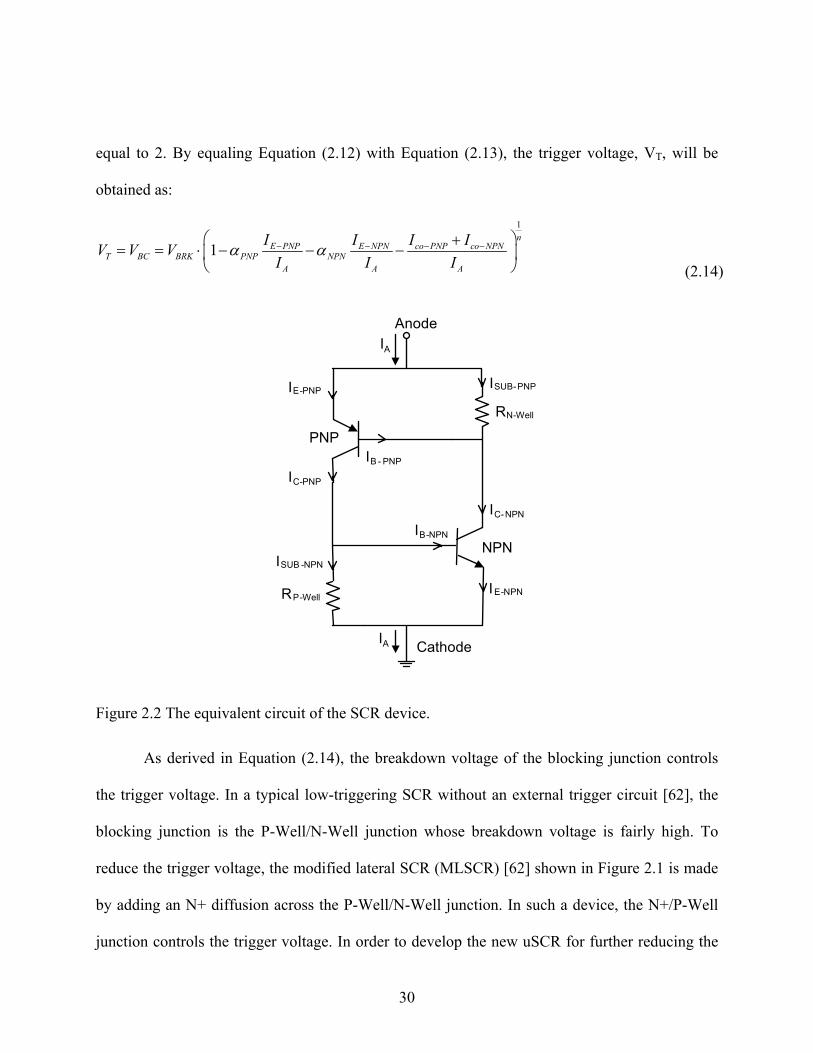
Cathode
Anode
RN-Well
RP-Well
PNP
NPN
IA
ISUB-PNP
IB - PNP
ISUB -NPN
IC-PNP
IE-NPN
IE-PNP
IC-NPN
IB-NPN
IA
Figure 2.2 The equivalent circuit of the SCR device.
As derived in Equation (2.14), the breakdown voltage of the blocking junction controls
the trigger voltage. In a typical low-triggering SCR without an external trigger circuit [62], the
blocking junction is the P-Well/N-Well junction whose breakdown voltage is fairly high. To
reduce the trigger voltage, the modified lateral SCR (MLSCR) [62] shown in Figure 2.1 is made
by adding an N+ diffusion across the P-Well/N-Well junction. In such a device, the N+/P-Well
junction controls the trigger voltage. In order to develop the new uSCR for further reducing the
31
trigger voltage, the N-type ESD (NESD) and P-type lightly-doped drain (PLDD) regions
(regions indicated with dashed lines in Figure 2.1) are added into the MLSCR through the LDD
ion implant step. The lengths, Ln and Lp, depict the NESD and PLDD region extensions. Lx is the
distance between the N+ and P+ regions (see Figure 2.1) and the silicide blocking mask covers
this region for the fully-salicided process. The variation of Ln and Lp is visualized in Figure 2.3.
When these two NESD and PLDD regions touch or overlap with each other (i.e., Ln+Lp ≥ Lx),
the NESD/PLDD junction takes over the N+/P-Well junction and becomes the dominant
blocking junction. The order of magnitude of doping levels for N+, P-Well, NESD and PLDD
are approximately 1020cm-3, 1017cm-3, 1019cm-3 and 1019cm-3, respectively. Since the depletion-
region width of the NESD/PLDD junction is much smaller than that of the N+/P-Well junction
under the same reverse-biased voltage, the former can breakdown at a smaller voltage than the
latter, which is able to make the SCR device triggered at much lower voltage.
P-Well
NESD PLDD
Silicide Blocking Layer
Lx
Ln Lp
Lx=1µm
Ln Lp
Ln Lp
N -Well
PLDD
Lx=1µm
Lx=1µm
Ln+Lp < Lx
Ln+Lp= Lx
Ln+Lp > Lx
Ln LpD5 D6
P-Well
PLDD
Silicide Blocking Layer
Lx
Ln Lp
Lx=1µm
Ln Lp
Ln Lp
N -Well
NESD PLDD
Lx=1µm
Lx=1µm
Ln+Lp < Lx
Ln+Lp= Lx
Ln+Lp > Lx
Ln LpD5 D
P-Well
NESD PLDD
Silicide Blocking Layer
Lx
Ln Lp
Lx=1µm
Ln Lp
Ln Lp
N -Well
PLDD
Lx=1µm
Lx=1µm
Ln+Lp < Lx
Ln+Lp= Lx
Ln+Lp > Lx
Ln LpD5 D6
P-Well
PLDD
Silicide Blocking Layer
Lx
Ln Lp
Lx=1µm
Ln Lp
Ln Lp
N -Well
NESD PLDD
Lx=1µm
Lx=1µm
Ln+Lp < Lx
Ln+Lp= Lx
Ln+Lp > Lx
Ln LpD5 D
Figure 2.3 Schematic diagram showing the different cases of Ln+Lp. Lx always keeps at 1μm.
32
A high and tunable holding voltage is desirable for latch-up immunity. On the
phenomenological level, the holding voltage depends on the degree of space charge
neutralization in the base regions of the p-n-p and n-p-n BJTs due to free carriers injected from
the emitter regions of the two BJTs. Hence, the lateral dimensions associated with the
neutralization area and injection area are the key parameters in designing the holding voltage.
For the uSCR shown in Figure 2.1, the holding voltage is tunable by changing the dimensions D3,
D5, D6 and D8.
For the negative characteristic of the uSCR device, the reverse breakdown and
conducting capability will be different when N-Well electrode is connected in two different ways.
Keeping the terminals, Emitter-NPN and P-Well, connected together as Cathode and tied to
ground, when N-Well is connected to Anode, the reverse breakdown voltage will approximate
the turn-on voltage of forward-biased p-n junction and the conduction current can be relatively
high. When N-Well is left open, the reverse breakdown voltage is about equal to VCEO of the
parasitic PNP BJT and the conducting capability is low. The normal operation of uSCR is to
keep N-Well connected to Anode. The connection way of N-Well open can be used to form a
dual direction SCR [63].
2.3. Experimental Results and Discussions
uSCR devices have been fabricated on a 0.35-μm fully-salicided BiCMOS process (see
Table 1.1). Their TLP I-V characteristics are plotted in Figure 2.4. The devices all have a width
of 100 μm and Lx of 1μm, while Ln and Lp are varied. The distance of anode to cathode keeps at
a (a has a value of more than 10 μm).
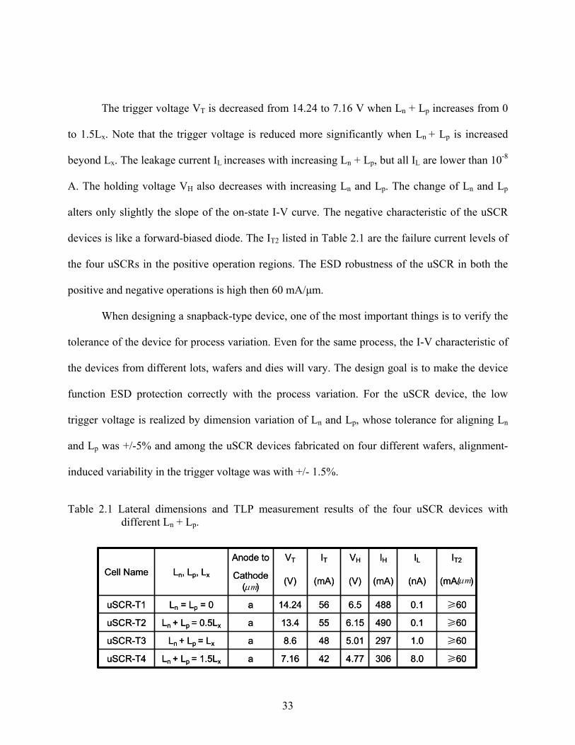
33
The trigger voltage VT is decreased from 14.24 to 7.16 V when Ln + Lp increases from 0
to 1.5Lx. Note that the trigger voltage is reduced more significantly when Ln + Lp is increased
beyond Lx. The leakage current IL increases with increasing Ln + Lp, but all IL are lower than 10-8
A. The holding voltage VH also decreases with increasing Ln and Lp. The change of Ln and Lp
alters only slightly the slope of the on-state I-V curve. The negative characteristic of the uSCR
devices is like a forward-biased diode. The IT2 listed in Table 2.1 are the failure current levels of
the four uSCRs in the positive operation regions. The ESD robustness of the uSCR in both the
positive and negative operations is high then 60 mA/μm.
When designing a snapback-type device, one of the most important things is to verify the
tolerance of the device for process variation. Even for the same process, the I-V characteristic of
the devices from different lots, wafers and dies will vary. The design goal is to make the device
function ESD protection correctly with the process variation. For the uSCR device, the low
trigger voltage is realized by dimension variation of Ln and Lp, whose tolerance for aligning Ln
and Lp was +/-5% and among the uSCR devices fabricated on four different wafers, alignment-
induced variability in the trigger voltage was with +/- 1.5%.
Table 2.1 Lateral dimensions and TLP measurement results of the four uSCR devices with different Ln + Lp.
a
a
a
a
Cathode( )
Anode to
8.0
1.0
0.1
0.1
(nA)
IL
306
297
490
488
(mA)
IH
≥604.77427.16Ln + Lp = 1.5LxuSCR-T4
≥605.01488.6Ln + Lp = LxuSCR-T3
≥606.155513.4Ln + Lp = 0.5LxuSCR-T2
≥606.55614.24Ln = Lp = 0uSCR-T1
(mA/ )(V)(mA)(V)
IT2VHITVT
Ln, Lp, LxCell Name
a
a
a
a
Cathode( )
Anode to
8.0
1.0
0.1
0.1
(nA)
IL
306
297
490
488
(mA)
IH
≥604.77427.16Ln + Lp = 1.5LxuSCR-T4
≥605.01488.6Ln + Lp = LxuSCR-T3
≥606.155513.4Ln + Lp = 0.5LxuSCR-T2
≥606.55614.24Ln = Lp = 0uSCR-T1
(mA/ )(V)(mA)(V)
IT2VHITVT
Ln, Lp, LxCell Namemμ
mμ
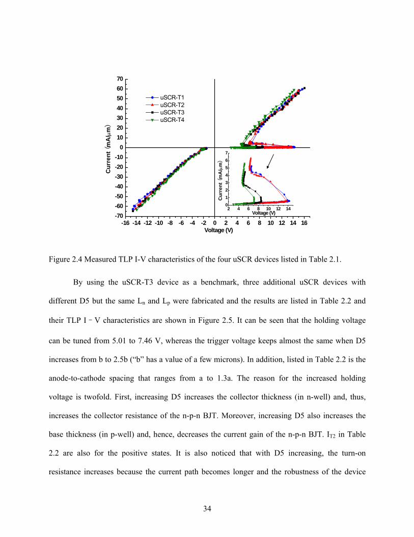
34
Figure 2.4 Measured TLP I-V characteristics of the four uSCR devices listed in Table 2.1.
By using the uSCR-T3 device as a benchmark, three additional uSCR devices with
different D5 but the same Ln and Lp were fabricated and the results are listed in Table 2.2 and
their TLP I–V characteristics are shown in Figure 2.5. It can be seen that the holding voltage
can be tuned from 5.01 to 7.46 V, whereas the trigger voltage keeps almost the same when D5
increases from b to 2.5b (“b” has a value of a few microns). In addition, listed in Table 2.2 is the
anode-to-cathode spacing that ranges from a to 1.3a. The reason for the increased holding
voltage is twofold. First, increasing D5 increases the collector thickness (in n-well) and, thus,
increases the collector resistance of the n-p-n BJT. Moreover, increasing D5 also increases the
base thickness (in p-well) and, hence, decreases the current gain of the n-p-n BJT. IT2 in Table
2.2 are also for the positive states. It is also noticed that with D5 increasing, the turn-on
resistance increases because the current path becomes longer and the robustness of the device
-16 -14 -12 -10 -8 -6 -4 -2 0 2 4 6 8 10 12 14 16-70-60-50-40-30-20-10
010203040506070
2 4 6 8 10 12 1401234567
Voltage (V)C
urre
nt (
mA
/μm)
C
urre
nt (
mA
/μm)
Voltage (V)
uSCR-T1 uSCR-T2 uSCR-T3 uSCR-T4
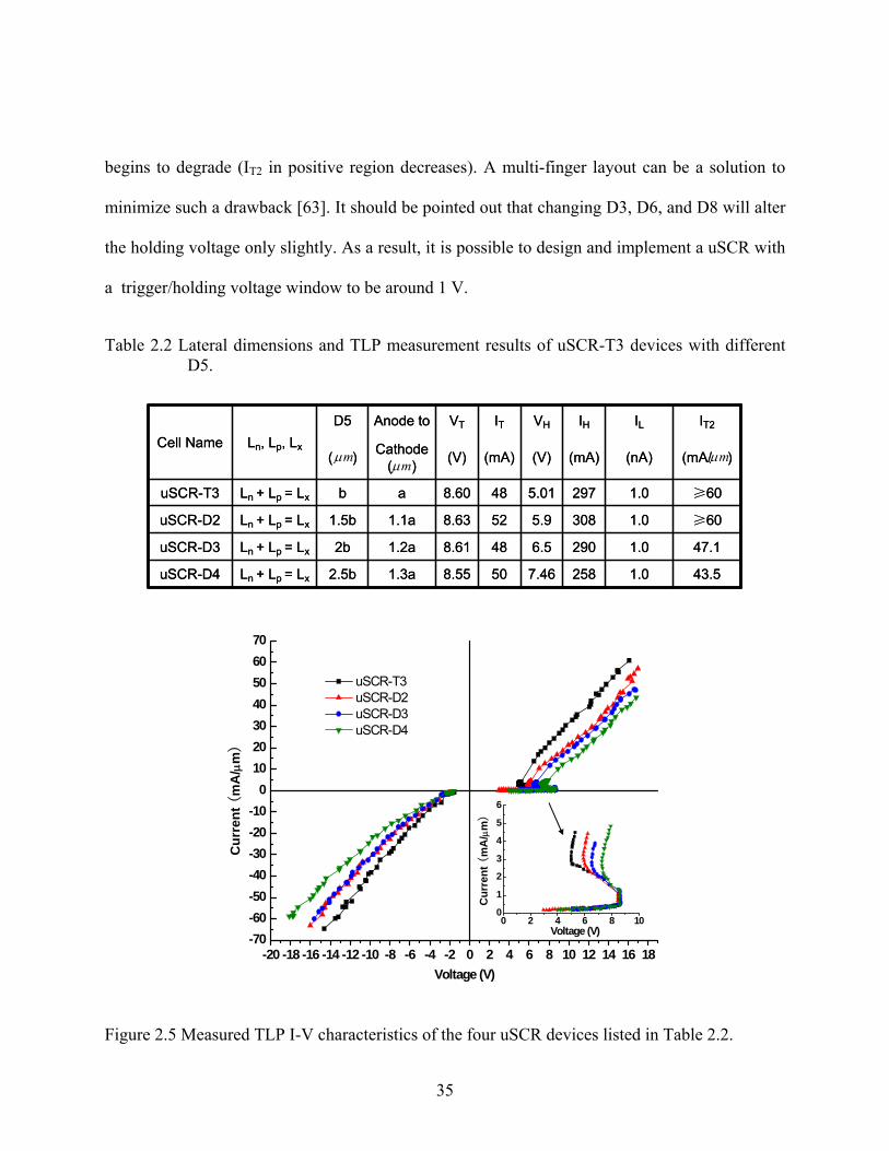
35
begins to degrade (IT2 in positive region decreases). A multi-finger layout can be a solution to
minimize such a drawback [63]. It should be pointed out that changing D3, D6, and D8 will alter
the holding voltage only slightly. As a result, it is possible to design and implement a uSCR with
a trigger/holding voltage window to be around 1 V.
Table 2.2 Lateral dimensions and TLP measurement results of uSCR-T3 devices with different D5.
1.0
1.0
1.0
1.0
(nA)
IL
1.3a
1.2a
1.1a
a
Cathode( )
Anode to
258
290
308
297
(mA)
IH
43.57.46508.552.5bLn + Lp = LxuSCR-D4
47.16.5488.612bLn + Lp = LxuSCR-D3
≥605.9528.631.5bLn + Lp = LxuSCR-D2
≥605.01488.60bLn + Lp = LxuSCR-T3
(mA/ )(V)(mA)(V)( )
IT2VHITVTD5Ln, Lp, LxCell Name
1.0
1.0
1.0
1.0
(nA)
IL
1.3a
1.2a
1.1a
a
Cathode( )
Anode to
258
290
308
297
(mA)
IH
43.57.46508.552.5bLn + Lp = LxuSCR-D4
47.16.5488.612bLn + Lp = LxuSCR-D3
≥605.9528.631.5bLn + Lp = LxuSCR-D2
≥605.01488.60bLn + Lp = LxuSCR-T3
(mA/ )(V)(mA)(V)( )
IT2VHITVTD5Ln, Lp, LxCell Name
mμmμmμ
Figure 2.5 Measured TLP I-V characteristics of the four uSCR devices listed in Table 2.2.
-20 -18 -16 -14 -12 -10 -8 -6 -4 -2 0 2 4 6 8 10 12 14 16 18-70-60-50-40-30-20-10
010203040506070
0 2 4 6 8 100
1
2
3
4
5
6
Voltage (V)
Cur
rent
(m
A/μ
m)
Cur
rent
(m
A/μ
m)
Voltage (V)
uSCR-T3 uSCR-D2 uSCR-D3 uSCR-D4

36
2.4. On-Chip Integration
The uSCR devices were integrated into a low-voltage IC and Figure 2.6(a) shows its on-
chip ESD protection scheme. This uSCR device is designed for the VSS-based ESD protection
scheme as shown in Figure 1.8. The anode terminals of the uSCR devices are all connected to the
pads and their cathode terminals are all connected to the common ground bus of the chip. The
TLP results show the ESD robustness of uSCR is as high as 60 mA/μm at both positive and
negative operation regions, the extra diode between supply and VSS in supply ESD protection
section and the primary ESD clamp for negative strikes in signal ESD protection section (in
Figure 1.8) can be removed to save area. The die size of the test chip is 1000*800 μm2 the
package type is 10-lead MicroPAK. The total width of the uSCR devices employed in this IC
chip are all 100 μm. Figure 2.6(b) is the equivalent circuit schematic diagram of the layout
showed in Figure 2.6(a). It illustrates the discharging current loops under the different JEDEC-
standard HBM and CDM zaps. The diode inside each uSCR cell denotes the device when it is
working in the negative operation. It can be seen that some discharging currents have to go
through positive- and negative-direction uSCR cells, for example, in the case of the HBM zap of
I/O pin vs. Vcc. The robustness of the uSCR in both directions can protect the chip up to +/- 8 kV
HBM and +/- 2 kV CDM stresses. Due to the robustness of the uSCR itself and no any
externally-assisted circuitry, each uSCR cell only consumes an area of about 2400 μm2.

37
Internal Circuitry
I/O Pad
I/O Pad
I/O Pad
I/O Pad
Vcc
GND
Internal Circuitry
Input Pin
OutputPin
Vcc
Vss
uSCR Cell
uSCRCell
uSCR Cell
uSCR
I/O Pad
I/O Pad
I/O Pad
I/O Pad
uSCR
uSCR
uSCR
uSCR
uSC
RuS
CR
uSC
RuS
CR
Ground Bus
Discharge current path of HBM zap of I/O pin vs. Vcc
Discharge current path of HBM zap of I/O pin vs. I/O pin
Discharge current path ofpositive CDM zap and
HBM zap of GND vs. I/O pin
Discharge current path ofnegative CDM zap and
HBM zap of I/O pin vs. GND
Internal Circuitry
I/O Pad
I/O Pad
I/O Pad
I/O Pad
Vcc
GND
Internal Circuitry
Input Pin
OutputPin
Vcc
Vss
uSCR Cell
uSCRCell
uSCR Cell
uSCR
I/O Pad
I/O Pad
I/O Pad
I/O Pad
uSCR
uSCR
uSCR
uSCR
uSC
RuS
CR
uSC
RuS
CR
Ground Bus
Discharge current path of HBM zap of I/O pin vs. Vcc
Discharge current path of HBM zap of I/O pin vs. I/O pin
Discharge current path ofpositive CDM zap and
HBM zap of GND vs. I/O pin
Discharge current path ofnegative CDM zap and
HBM zap of I/O pin vs. GND
Figure 2.6 (a) Scheme of the on-chip ESD protection realized with the uSCR device. (b) Equivalent circuit schematic diagram of the layout showed in (a). It shows the discharge current loops under the different HBM and CDM zaps.
The proposed uSCR in this chapter with a trigger voltage lower than 8 V, a holding
voltage higher than 6 V, an ESD robustness higher than 60 mA/μm and an HBM as well as a
CDM ESD-protection levels as high as +/- 8 kV and +/- 2 kV, respectively, is one of the most
advanced ESD devices to date for low-voltage ESD-protection applications.
(a)
(b)
38
2.5. Chapter Summary
As technology advances, the requirement for the trigger and holding voltages of the ESD
devices becomes more stringent. This chapter starts with discussion of the triggering mechanism
of the SCR device then presents a novel low trigger-/high holding-voltage SCR devices, called
uSCR, which have been successfully designed, fabricated and characterized on a 0.35 μm
BiCMOS process. Experimental results have verified that the trigger voltage can be reduced to
less than 8 V without using any external trigger circuitry and that the holding voltage can be
increased to more than 6 V without sacrificing the ESD robustness. The ESD robustness of the
uSCR device makes it be used as an area efficient ESD protection cell in VSS-based ESD
protection scheme. The area efficiency is realized by three factors:
1. The uSCR device itself is robust, with a IT2 higher than 60 mA/μm at both
forward and reverse operation region.
2. When apply the uSCR device in VSS-based ESD protection scheme, the extra
diode for negative ESD strike can be removed, with relaying on the uSCR
device to dump the ESD current of negative strike.
3. Comparing with VDD-based ESD protection scheme, the VSS-based ESD
protection scheme dose not have to involve an ESD clamp between I/O pad and
VDD.
39
CHAPTER 3. DEVELOPMENT OF HIGH HOLDING CURRENT SCR FOR HIGH VOLTAGE ESD PROTECTION APPLICATIONS
3.1. Introduction
High voltage technologies have been developed by extending mature, less expensive
CMOS technologies (0.18 μm and above) with new features for specific automotive or consumer
electronics products, etc, which offers significant economical advantages in this competitive
market segment [76]. The new features, such as equipping the MOS transistors with thick gate
oxides and lowly doped drain/source implants to increase the voltage tolerance of the devices,
allows driving the maximum operating voltages to the limits of the process technology. The ESD
protection cells for the high voltage technologies need to be able to withstand the high voltages.
However, these new technology features will significantly degrade the high current performance
of conventional protection devices.
ESD related issues in high voltage technologies including: 1) Strong snapback. The
additional feature in high voltage technology, low doping implants, will strongly impact the
snapback behavior of conventional snapback ESD protection device, like ggNMOS. The holding
voltage of the ggNMOS for high voltage technologies are far away below operation voltage, VDD.
This is due to Kirk effect [77]-[78]. Also, the ggNMOS shows the immediate degradation after
snapback. 2) Intrinsic high voltage NMOS reliability issues due to high voltage and high current
applications. 3) Multi-finger non- uniformly triggering. The Murphy’s law always prefers to turn
on one MOSFET finger ahead of any other ones. The condition, VT1 (the trigger voltage) < VT2

40
(the thermal runaway voltage), needs to meet to make other fingers come to play together before
the first-turn-on finger fails, especially for the silicide technologies. It is hard to make VT1 < VT2
valid in high voltage technologies [79]. 4) Latchup risk. Due to the strong snapback, transient
latchup may occur due to the low holding voltage of the ESD protection cell. 5) High series
resistance, which is due to the increasing critical distance in high voltage technologies to avoid
punch through when the lightly doped diffusions make the depletion region wider. 6) The
triggering competition between the weak output driver and the parallel ESD clamp are tougher in
high voltage technologies.
We have discussed in previous chapters that the SCR device has long been used as a
robust and area-efficient on-chip ESD protection device. Its inherent regenerative feedback
mechanism leads to a deep-snapback characteristic with a relatively small holding voltage [80].
This reduces the power dissipation in the SCR during the ESD event and makes the SCR device
more robust than other ESD devices such as diodes and GGNMOS [81].
The SCR device is one of the good candidate devices to be used for high voltage ESD
protection [76]. When using SCR devices for ESD protection of high voltage ICs, the transient
trigger voltage needs to be tailored to meet high voltage application. Also, the small holding
voltage will become problematic, especially for the case of a supply clamp. The VDD is much
higher for high voltage applications than that when the technology is for CMOS low voltage
application, for example, VDD can be from 5 V to 65 V and higher. The low holding voltage
would allow the SCR to remain in its low conductive state after the ESD event dissipated if the
holding voltage is smaller than the supply voltage. And the SCR-based devices with low holding
41
voltage would interfere with the normal circuit operation when accidentally triggered on by noise
pulses, which is known as the ESD-induced latchup [49].
There are two solutions to avoid such kind of latchup. One is to increase the holding
voltage (VH) to be greater than the maximum voltage supply of VDD [82]-[83], which either has
to stack several ESD protection devices by consuming a large layout area [82] or has to sacrifice
the robustness [83] which is right the advantage of SCR-based devices due to the relatively low
holding voltage. Another solution is to increase the triggering current [68] or the holding current
of the SCR devices [69]. As shown in Figure 3.1, if the SCR device has an holding current (IH)
higher than certain latchup-immune current (ILU), the latchup due to ESD device false triggering
can be avoided during normal operation as well as under the overshooting and undershooting
noise pulses. Additionally, since the requirement of VH > VDD can be dropped, the failure current
(IT2) of the SCR device can be higher, comparing with the other latchup-immune solution which
requires VH > VDD. By doing this way, the big advantage of high failure current of the SCR
device due to deep-snapback can be utilized well. Literature [68]-[69] have reported such SCR
devices with high IH for latchup-free solutions, but both cases have to involve ground-gate MOS
devices which normally will incur serious reliability weakness issues for high voltage
technologies [76].
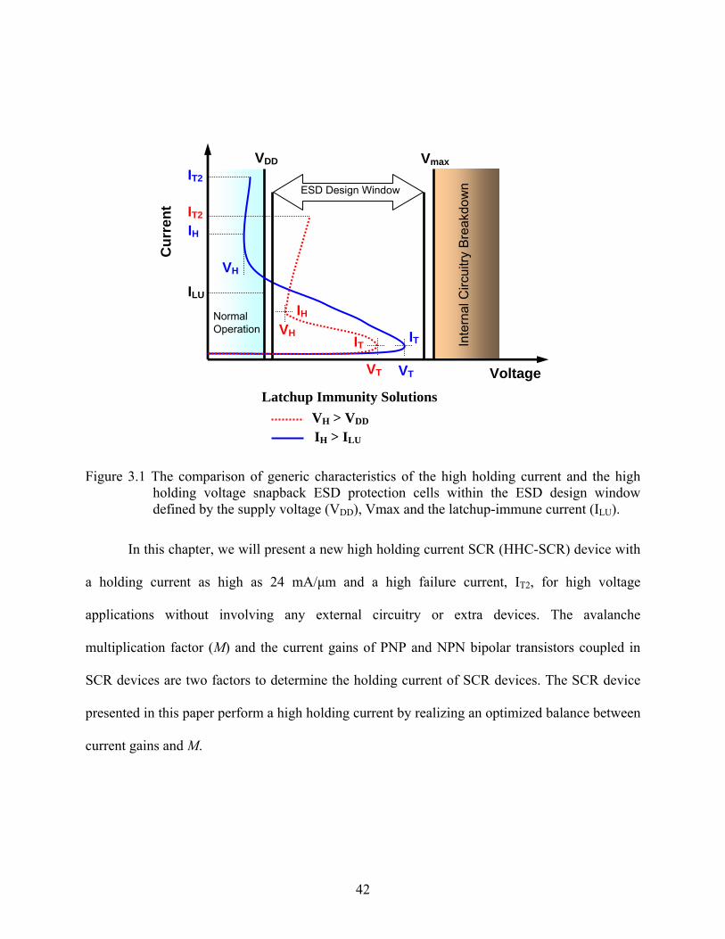
42
Figure 3.1 The comparison of generic characteristics of the high holding current and the high holding voltage snapback ESD protection cells within the ESD design window defined by the supply voltage (VDD), Vmax and the latchup-immune current (ILU).
In this chapter, we will present a new high holding current SCR (HHC-SCR) device with
a holding current as high as 24 mA/μm and a high failure current, IT2, for high voltage
applications without involving any external circuitry or extra devices. The avalanche
multiplication factor (M) and the current gains of PNP and NPN bipolar transistors coupled in
SCR devices are two factors to determine the holding current of SCR devices. The SCR device
presented in this paper perform a high holding current by realizing an optimized balance between
current gains and M.
ESD Design Window
Normal Operation
Inte
rnal
Circ
uitry
Bre
akdo
wn
VT
IT
IH
IT2
VH
VDD Vmax
Voltage
Cur
rent
ILU
VH IH
VT
IT
IT2
Latchup Immunity Solutions VH > VDD IH > ILU
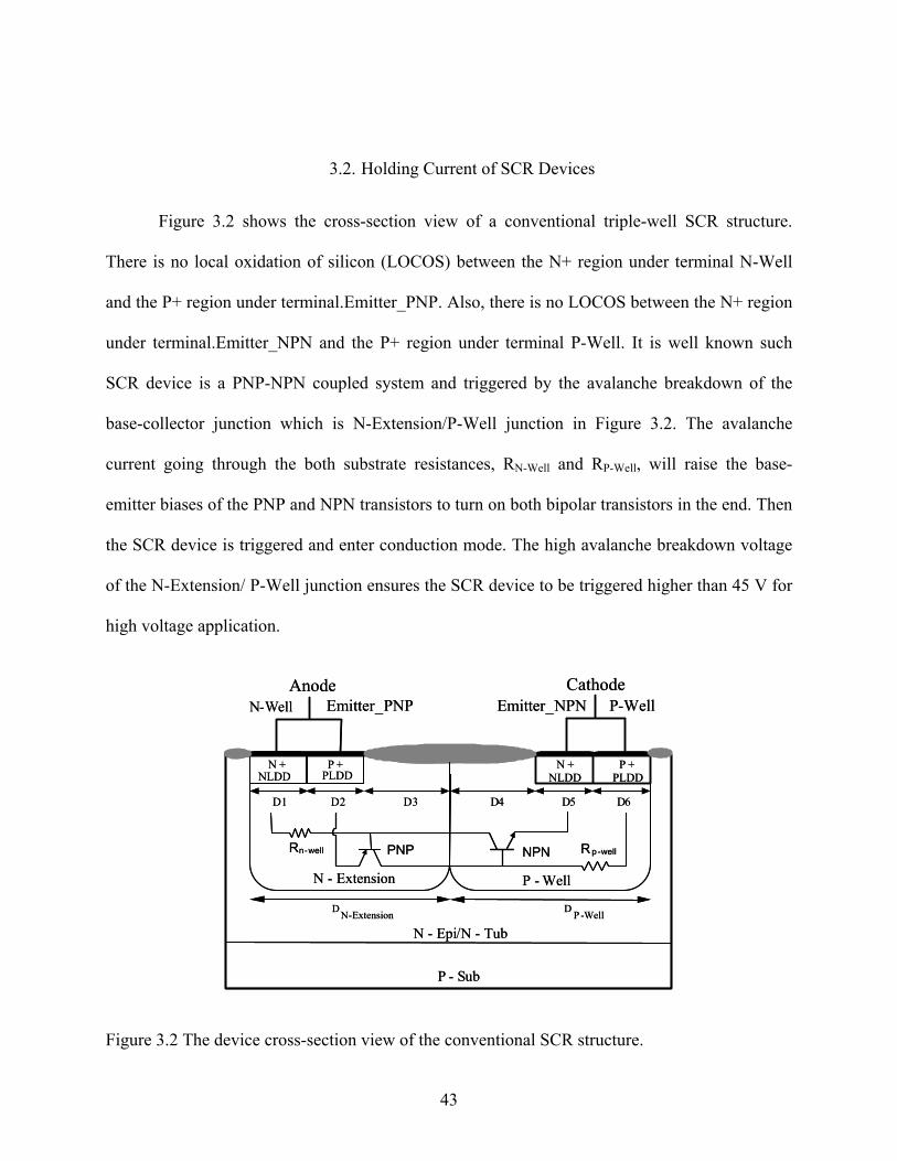
43
3.2. Holding Current of SCR Devices
Figure 3.2 shows the cross-section view of a conventional triple-well SCR structure.
There is no local oxidation of silicon (LOCOS) between the N+ region under terminal N-Well
and the P+ region under terminal.Emitter_PNP. Also, there is no LOCOS between the N+ region
under terminal.Emitter_NPN and the P+ region under terminal P-Well. It is well known such
SCR device is a PNP-NPN coupled system and triggered by the avalanche breakdown of the
base-collector junction which is N-Extension/P-Well junction in Figure 3.2. The avalanche
current going through the both substrate resistances, RN-Well and RP-Well, will raise the base-
emitter biases of the PNP and NPN transistors to turn on both bipolar transistors in the end. Then
the SCR device is triggered and enter conduction mode. The high avalanche breakdown voltage
of the N-Extension/ P-Well junction ensures the SCR device to be triggered higher than 45 V for
high voltage application.
N + P +
P - Sub
N - Epi/N - Tub
N-Well Emitter_PNP Emitter_NPN P-WellAnode Cathode
D1
D N-Extension D P -Well
NLDD PLDDN +
NLDDP +
PLDD
Rp-wellNPNPNP
P - WellN - Extension
Rn-well
D2 D3 D4 D5 D6
N + P +
P - Sub
N - Epi/N - Tub
N-Well Emitter_PNP Emitter_NPN P-WellAnode Cathode
D1
D N-Extension D P -Well
NLDD PLDDN +
NLDDP +
PLDD
Rp-wellNPNPNP
P - WellN - Extension
Rn-well
D2 D3 D4 D5 D6
Figure 3.2 The device cross-section view of the conventional SCR structure.
44
The SCR device physics before triggering has been discussed in detail in Chapter 2.Here
will discuss the state after the SCR device triggers. Figure 3.3 is the equivalent circuit of the
SCR device, showing all the directions of electron and hole currents after the SCR triggers,
which means both PNP and NPN transistors turn on. Igen is avalanche generation current. Igen is a
function of the avalanche multiplication factor, M, in the high electrical field region. Igen due to
an incident current Ip is given by [84]:
( 1)gen pI M I= − ⋅ (3.1)
M is also expressed as Equation (2.13). Before SCR device triggers, Ip is solely due to thermal
generation and minority carrier diffusion. Igen only supplies the ISUB-PNP and ISUB-NPN. As both
bipolar transistors turn on, Igen will also supply IB-PNP and IB-NPN in additional to ISUB-PNP and ISUB-
NPN. But the bipolar current, IC-PNP and IC-NPN, now provide additional current sources for
multiplication. Equation (3.1) can be rewritten as:
( 1) ( )gen p C PNP C NPNI M I I I− −= − ⋅ + + (3.2)
Thus, the value of M required to sustain both bipolar devices in the on states can be reduced and
voltage snapback is observed where the voltage at Anode drops to a sustaining level, VH. IC-PNP
and IC-NPN are functions of current gains of both intrinsic PNP and NPN transistors, βPNP and βNPN.
The requirement that the SCR device stays latched is given by [85]:
1 1 11 11 1PNP NPN
M
β β
⎛ ⎞⎜ ⎟⎜ ⎟+ ≥⎜ ⎟+ +⎜ ⎟⎝ ⎠ (3.3)
The holding voltage VH is reached by coming to a balance between M and βPNP & βNPN. If the
βPNP and βNPN are bigger, which means IC-PNP + IC-NPN (see equation (3.2)) will be bigger, the M
45
will be less resulting a smaller VH, vice versa. The corresponding current when the SCR device
reaches VH is the holding current, IH, which can be expressed as (as shown in Figure 3.3):
H SUB PNP E PNPI I I− −= + (3.4)
SUB PNP gen C NPN B PNPI I I I− − −= + − (3.5)
Since the Ip is much smaller comparing with IC-PNP and IC-NPN after the device turns on, we can
get the relationship:
( 1) ( )gen C PNP C NPN genI M I I I− −≈ − ⋅ + = (3.6)
C PNPE PNP
PNP
IIα
−− =
(3.7)
C PNPB PNP
PNP
IIβ−
− = (3.8)
By replacing (3.6), (3.7), (3.8) and (3.9) in (3.5), we finally have:
( )H C PNP C NPNI M I I− −= ⋅ + (3.9)
As the aforementioned, an increasing of IC-PNP+IC-NPN will normally cause M decreasing.
So the high holding current will be realized by designing a SCR structure with a maximal M(IC-
PNP+IC-NPN), which means to find an optimized combination of M and βPNP & βNPN.
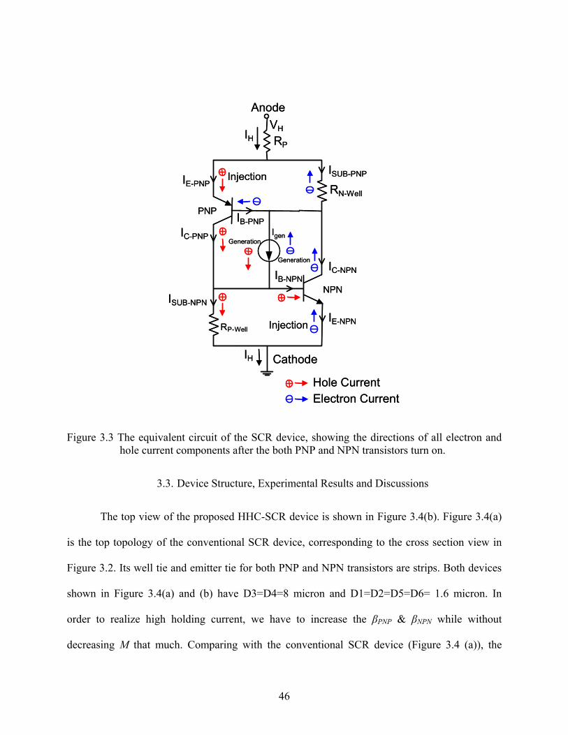
46
Cathode
Anode
RP-Well
PNP
NPN
Injection
Injection
Generation
Generation
Hole CurrentElectron Current
IE-PNP
IE-NPN
IC-NPNIB-NPN
IC-PNP
ISUB-NPN
RN-Well
ISUB-PNP
IB-PNPIgen
IHVH
RP
IH Cathode
Anode
RP-Well
PNP
NPN
Injection
Injection
Generation
Generation
Hole CurrentElectron Current
IE-PNP
IE-NPN
IC-NPNIB-NPN
IC-PNP
ISUB-NPN
RN-Well
ISUB-PNP
IB-PNPIgen
IHVH
RP
IH
Figure 3.3 The equivalent circuit of the SCR device, showing the directions of all electron and hole current components after the both PNP and NPN transistors turn on.
3.3. Device Structure, Experimental Results and Discussions
The top view of the proposed HHC-SCR device is shown in Figure 3.4(b). Figure 3.4(a)
is the top topology of the conventional SCR device, corresponding to the cross section view in
Figure 3.2. Its well tie and emitter tie for both PNP and NPN transistors are strips. Both devices
shown in Figure 3.4(a) and (b) have D3=D4=8 micron and D1=D2=D5=D6= 1.6 micron. In
order to realize high holding current, we have to increase the βPNP & βNPN while without
decreasing M that much. Comparing with the conventional SCR device (Figure 3.4 (a)), the
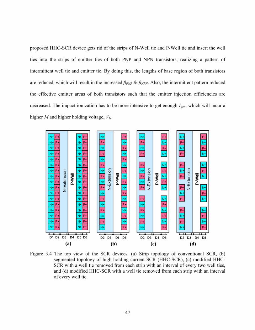
47
proposed HHC-SCR device gets rid of the strips of N-Well tie and P-Well tie and insert the well
ties into the strips of emitter ties of both PNP and NPN transistors, realizing a pattern of
intermittent well tie and emitter tie. By doing this, the lengths of base region of both transistors
are reduced, which will result in the increased βPNP & βNPN. Also, the intermittent pattern reduced
the effective emitter areas of both transistors such that the emitter injection efficiencies are
decreased. The impact ionization has to be more intensive to get enough Igen, which will incur a
higher M and higher holding voltage, VH.
P+
N+
P+
N+
P+
N+
P+
N+
P+
N+
P+
N+
P+
N+
P+
N+
N+
P+
P+
N+
P+
N+
P+
N+
P+
N+
P+
N+
P+
N+
P+
N+
N+
P+
D2 D3 D4 D5
N-E
x ten
s ion
P-W
ell
P+
N+
P+
N+
P+
P+
N+
P+
P+
N+
P+
P+
N+
N+
P+
P+
N+
N+
P+
N+
N+
P+
N+
N+
P+
N+
N+
P+
D2 D3 D4 D5
N-E
x ten
sion
P-W
ell
P+
N+
P+
N+
P+
P+
N+
P+
N+
P+
P+
N+
P+
N+
N+
P+
P+
N+
N+
P+
N+
P+
N+
N+
P+
N+
P+
N+
N+
P+
D2 D3 D4 D5
N-E
x ten
sion
P-W
ell
N+
N+
N+
N+
N+
N+
N+
N+
N+
N+
N+
N+
N+
N+
N+
N+
N+
P+
P+
P+
P+
P+
P+
P+
P+
P+
P+
P+
P+
P+
P+
P+
P+
P+
D1 D2 D3 D6D4 D5
N-E
xten
sion
P -W
ell
P+
P+
P+
P+
P+
P+
P+
P+
P+
P+
P+
P+
P+
P+
P+
P+
P+
N+
N+
N+
N+
N+
N+
N+
N+
N+
N+
N+
N+
N+
N+
N+
N+
N+
P+
N+
P+
N+
P+
N+
P+
N+
P+
N+
P+
N+
P+
N+
P+
N+
N+
P+
P+
N+
P+
N+
P+
N+
P+
N+
P+
N+
P+
N+
P+
N+
N+
P+
D2 D3 D4 D5
N-E
x ten
s ion
P-W
ell
P+
N+
P+
N+
P+
P+
N+
P+
P+
N+
P+
P+
N+
N+
P+
P+
N+
N+
P+
N+
N+
P+
N+
N+
P+
N+
N+
P+
D2 D3 D4 D5
N-E
x ten
sion
P-W
ell
P+
N+
P+
N+
P+
P+
N+
P+
N+
P+
P+
N+
P+
N+
N+
P+
P+
N+
N+
P+
N+
P+
N+
N+
P+
N+
P+
N+
N+
P+
D2 D3 D4 D5
N-E
x ten
sion
P-W
ell
N+
N+
N+
N+
N+
N+
N+
N+
N+
N+
N+
N+
N+
N+
N+
N+
N+
P+
P+
P+
P+
P+
P+
P+
P+
P+
P+
P+
P+
P+
P+
P+
P+
P+
D1 D2 D3 D6D4 D5
N-E
xten
sion
P -W
ell
P+
P+
P+
P+
P+
P+
P+
P+
P+
P+
P+
P+
P+
P+
P+
P+
P+
N+
N+
N+
N+
N+
N+
N+
N+
N+
N+
N+
N+
N+
N+
N+
N+
N+
Figure 3.4 The top view of the SCR devices. (a) Strip topology of conventional SCR, (b) segmented topology of high holding current SCR (HHC-SCR), (c) modified HHC-SCR with a well tie removed from each strip with an interval of every two well ties, and (d) modified HHC-SCR with a well tie removed from each strip with an interval of every well tie.
(b) (c) (d) (a)
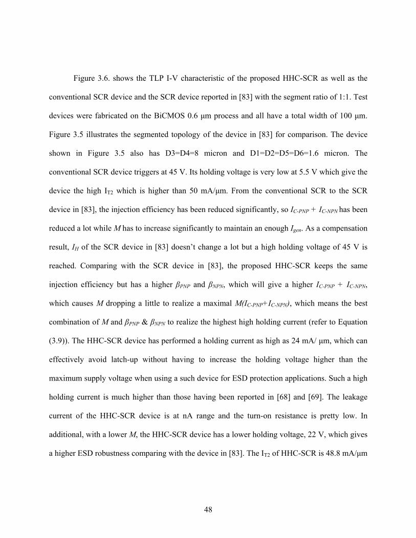
48
Figure 3.6. shows the TLP I-V characteristic of the proposed HHC-SCR as well as the
conventional SCR device and the SCR device reported in [83] with the segment ratio of 1:1. Test
devices were fabricated on the BiCMOS 0.6 μm process and all have a total width of 100 μm.
Figure 3.5 illustrates the segmented topology of the device in [83] for comparison. The device
shown in Figure 3.5 also has D3=D4=8 micron and D1=D2=D5=D6=1.6 micron. The
conventional SCR device triggers at 45 V. Its holding voltage is very low at 5.5 V which give the
device the high IT2 which is higher than 50 mA/μm. From the conventional SCR to the SCR
device in [83], the injection efficiency has been reduced significantly, so IC-PNP + IC-NPN has been
reduced a lot while M has to increase significantly to maintain an enough Igen. As a compensation
result, IH of the SCR device in [83] doesn’t change a lot but a high holding voltage of 45 V is
reached. Comparing with the SCR device in [83], the proposed HHC-SCR keeps the same
injection efficiency but has a higher βPNP and βNPN, which will give a higher IC-PNP + IC-NPN,
which causes M dropping a little to realize a maximal M(IC-PNP+IC-NPN), which means the best
combination of M and βPNP & βNPN to realize the highest high holding current (refer to Equation
(3.9)). The HHC-SCR device has performed a holding current as high as 24 mA/ μm, which can
effectively avoid latch-up without having to increase the holding voltage higher than the
maximum supply voltage when using a such device for ESD protection applications. Such a high
holding current is much higher than those having been reported in [68] and [69]. The leakage
current of the HHC-SCR device is at nA range and the turn-on resistance is pretty low. In
additional, with a lower M, the HHC-SCR device has a lower holding voltage, 22 V, which gives
a higher ESD robustness comparing with the device in [83]. The IT2 of HHC-SCR is 48.8 mA/μm
49
versus 28 mA/μm in [83] which relies on increasing VH to be higher than VDD to realize the
latchup immunity. And the IT2 of HHC-SCR is almost as good as that of the conventional SCR.
N+
N+
N+
N+
N+
N+
N+
N+
N+
N+
N+
N+
N+
N+
N+
N+
N+
P+
P+
P+
P+
P+
P+
P+
P+
P+
P+
P+
P+
P+
P+
P+
P+
P+
P+
N+
P+
N+
P+
N+
P+
N+
P+
N+
P+
N+
P+
N+
P+
N+
N+
P+
D1
P+
N+
P+
N+
P+
N+
P+
N+
P+
N+
P+
N+
P+
N+
N+
P+
D2 D3 D6D4 D5
N-E
xten
sion
P-W
ell
N+
N+
N+
N+
N+
N+
N+
N+
N+
N+
N+
N+
N+
N+
N+
N+
N+
P+
P+
P+
P+
P+
P+
P+
P+
P+
P+
P+
P+
P+
P+
P+
P+
P+
P+
N+
P+
N+
P+
N+
P+
N+
P+
N+
P+
N+
P+
N+
P+
N+
N+
P+
D1
P+
N+
P+
N+
P+
N+
P+
N+
P+
N+
P+
N+
P+
N+
N+
P+
D2 D3 D6D4 D5
N-E
xten
sion
P-W
ell
Figure 3.5 The illustration of the segment topology of the SCR device reported in reference [83].
The further increasing of βPNP and βNPN are also performed to verify the maximal M(IC-
PNP+IC-NPN) has been reached. Taking the proposed HHC-SCR in Figure 3.4(b) as a benchmark,
which has a D3=D4=8 micron, D3=D4 is reduced from 8.0 micro to 2.0 micron, which cause
βPNP and βNPN increasing. Figure 3.6 shows the TLP measurement results of HHC-SCR with
different D3 and D4. It can be seen that when D3=D4 decrease, the lengths of base region of
both transistors are reduced, which will result in the increased βPNP & βNPN then the increased IC-
PNP + IC-NPN. However, the holding voltage decreases since M has decreased. As the result, the
overall holding current, which is the product of M and IC-PNP + IC-NPN, drops from 24 mA/μm to
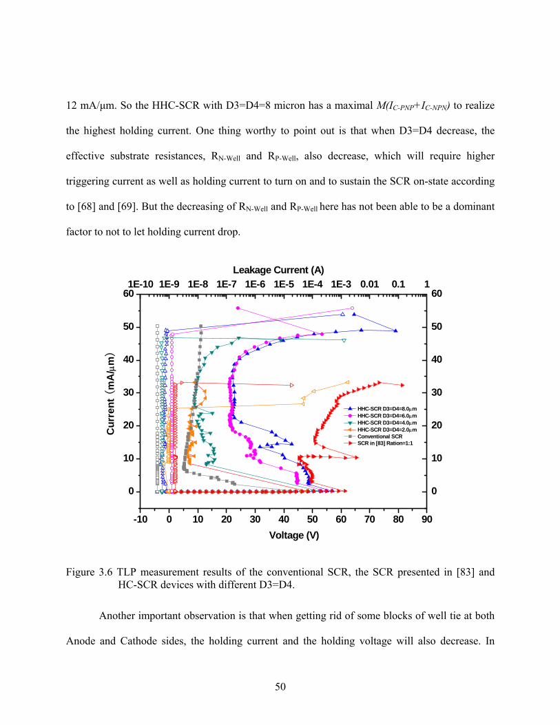
50
12 mA/μm. So the HHC-SCR with D3=D4=8 micron has a maximal M(IC-PNP+IC-NPN) to realize
the highest holding current. One thing worthy to point out is that when D3=D4 decrease, the
effective substrate resistances, RN-Well and RP-Well, also decrease, which will require higher
triggering current as well as holding current to turn on and to sustain the SCR on-state according
to [68] and [69]. But the decreasing of RN-Well and RP-Well here has not been able to be a dominant
factor to not to let holding current drop.
-10 0 10 20 30 40 50 60 70 80 90
0
10
20
30
40
50
601E-10 1E-9 1E-8 1E-7 1E-6 1E-5 1E-4 1E-3 0.01 0.1 1
0
10
20
30
40
50
60
C
urre
nt (
mA
/μm)
Voltage (V)
Leakage Current (A)
HHC-SCR D3=D4=8.0μm HHC-SCR D3=D4=6.0μm HHC-SCR D3=D4=4.0μm HHC-SCR D3=D4=2.0μm Conventional SCR SCR in [83] Ration=1:1
Figure 3.6 TLP measurement results of the conventional SCR, the SCR presented in [83] and HC-SCR devices with different D3=D4.
Another important observation is that when getting rid of some blocks of well tie at both
Anode and Cathode sides, the holding current and the holding voltage will also decrease. In
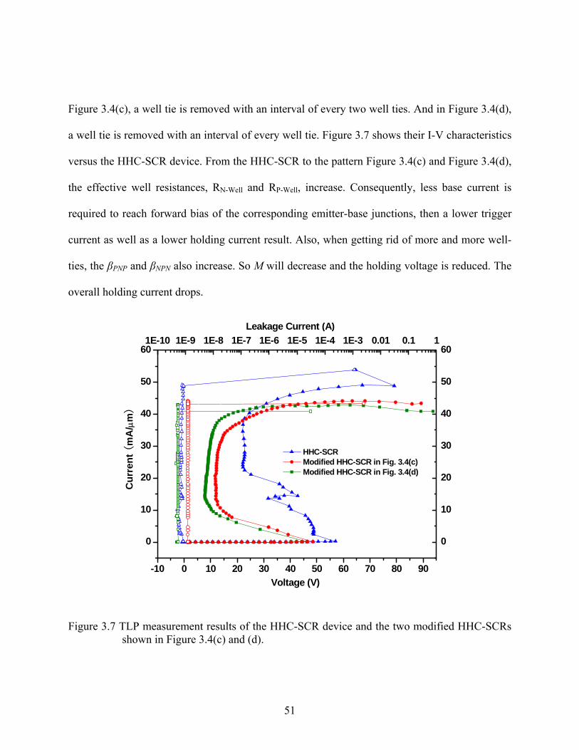
51
Figure 3.4(c), a well tie is removed with an interval of every two well ties. And in Figure 3.4(d),
a well tie is removed with an interval of every well tie. Figure 3.7 shows their I-V characteristics
versus the HHC-SCR device. From the HHC-SCR to the pattern Figure 3.4(c) and Figure 3.4(d),
the effective well resistances, RN-Well and RP-Well, increase. Consequently, less base current is
required to reach forward bias of the corresponding emitter-base junctions, then a lower trigger
current as well as a lower holding current result. Also, when getting rid of more and more well-
ties, the βPNP and βNPN also increase. So M will decrease and the holding voltage is reduced. The
overall holding current drops.
-10 0 10 20 30 40 50 60 70 80 90
0
10
20
30
40
50
601E-10 1E-9 1E-8 1E-7 1E-6 1E-5 1E-4 1E-3 0.01 0.1 1
0
10
20
30
40
50
60
HHC-SCR Modified HHC-SCR in Fig. 3.4(c) Modified HHC-SCR in Fig. 3.4(d)
Leakage Current (A)
Voltage (V)
Cur
rent
(m
A/μ
m)
Figure 3.7 TLP measurement results of the HHC-SCR device and the two modified HHC-SCRs shown in Figure 3.4(c) and (d).
52
3.4. Chapter Summary
Preventing latchup is an important issue in the design and realization of on-chip ESD
protection solutions for high voltage integrated circuits. This can be achieved by using ESD
devices having a high holding voltage and/or high holding current. To this end, a novel high
holding current SCR (HHC-SCR) has been presented in this chapter for high voltage applications
and test devices have been fabricated on the BiCMOS 0.6 μm process. The holding current of
SCR device is dependent on the avalanche multiplication factor, M, and the current gains of the
PNP and NPN transistors in SCR device. The TLP measurement results have shown that by
reaching a maximal M(IC-PNP+IC-NPN), the HHC-SCR device has realized a holding current as
high as 24 mA/μm to effectively avoid latch-up and a high failure current (48 mA/μm) for ESD
robustness. Additionally, without involving any external circuitry or extra devices, the HHC-
SCR device releases reliability weakness issues and accomplishes the minimum area
consumption.
53
CHAPTER 4. COMPREHENSIVE COMPACT MODELING OF SCR DEVICES FOR CDM ESD SIMULATION OF COMPLETE I/O CIRCUITS
4.1. Introduction
The CDM ESD event has been discussed in Chapter 1. The first use of CDM test method
was reported in by Bossard et al. in [86]. The increased usage of automated manufacturing and
testing equipment has led to environments that are more likely to have the presence of the CDM
ESD event, rather than the more well-known HBM. As such, the CDM is becoming more and
more widely used for defining the ESD stress and reliability in the semiconductor industry. The
CDM possesses pulses that can reach several Amps in a few tenth of nano second. In addition the
waveform of the current associated with the CDM is oscillatory (see Figure 1.6). These issues
make the development of an accurate and compact model for CDM ESD devices very difficult,
but such a model is urgently needed in the research and development of effective and robust
CDM ESD protection solutions for a wide range of integrated circuits.
Normally, the ESD protection SCR devices have been designed through simulations by
using either technology computer aided design (TCAD) tools or through experimental approach,
which is also called trial-and-error iterations. The former is normally time-consuming and it is
difficult to include both ESD protection cells and the protected core circuits into the TCAD
simulation. The latter way also has to wait the entire cycle of test chip to get results and cost
more money to run more rounds of trial if the first round doesn’t succeed. Additionally, there is
interaction between ESD protection cells and core circuits. On one hand, ESD protection cell
54
will incur adverse parasitic effects to core circuits, such as extra parasitic capacitance and noise,
which is a disaster especially for high speed and radio frequency (RF) ICs. On the other hand,
the performance of ESD protection cells will be impact by core circuits. A working stand-alone
ESD protection unit does not warrant chip level ESD protection 0. So comparing with device
simulations and iterative experiments, design engineers prefer to employ compact models in a
circuit simulator to get faster prediction of the ESD protection level of the whole chip and do co-
design of the ESD and functional circuitry at the pre-silicon stage.
Even though SCR in one of the most important ESD protection devices, SCR compact
model is not widely available since most available design tools, such as SPICE, do not contain
the standard model of SCR and SCR devices for ESD protection operate in high-current and
breakdown regimes which regular circuit models do not cover. A few SCR compact models have
been reported in the literature. Juliano and Rosenbaum developed a model based on the Verilog-
A coded behavior modeling to describe the SCR snapback [87]-[88], but a smoothing function
has to be used to ensure continuity. Another model was built from a macromodel consisting of
existing device models, but additional auxiliary current and voltage sources have to be added to
properly describe the breakdown behavior in the SCR [89]-[90], an approach that is hard-coded
in simulators and lacks flexibility when the technology is changed. Zhou et al. mentioned that an
advanced BJT model can be used as the backbone for the SCR compact modeling [91]-[92]. This
model doesn’t describe the CDM-relevant features, such as the device characteristics in negative
operation and the substrate element modeling. Therefore it is not applicable for the simulation of
I/O circuits subject to the CDM ESD stress.
55
In this chapter, we seek to develop a comprehensive compact model for the high-holding,
low-triggering SCR (HH-LVTSCR) [93] used to provide CDM ESD protection at the I/O pin of
CMOS circuits. Section 3.2 will focus on model development and model implementation, as well
as the discussion of apposite model parameter extraction. Special attention is given to accurately
describing the CDM-relevant operation states. This is followed by the presentation of the
modeling results and verification for SCR operations based on TLP technique in Section 4.3. In
order to achieve accurate simulation of CDM events, proper characterization of the CDM tester
is just as critical as the device modeling. A JEDEC-standard CDM waveform created by a
calibrated series RLC circuit is presented in Section 4.4. And this section will demonstrate the
application of the new SCR model on a 0.35 μm CMOS circuit under the CDM stress, and the
model will successfully explain as to why the input-only pins of the circuit have lower CDM
robustness than the output-only pins [94].
4.2. SCR Compact Model Development
The cross section of a HH-LVTSCR is shown in Figure 4.1(a). The device is considered
here to illustrate the model development, but the modeling approach applies generally to other
SCR devices. The terminal connection of the HH-LVTSCR device in typical ESD applications is
shown in Figure 4.1(a) as well. The N-Well and Emitter-PNP terminals are connected to the
Anode. The Gate, Emitter-NPN, P-Well and Substrate terminals are tied together to be the
Cathode.
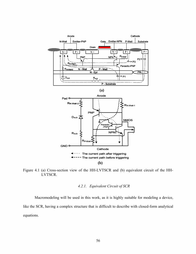
56
N - Well
P - Substrate
N - Epi
N-Well Gate
P - Well
Anode Cathode
Drain
N + P +
Substrate
RP-Well
Rsub
RN-Well -1
NPNPNP
Dsub
P-Well
N + N + P + P +
Emitter-PNP Emitter-NPN
RN-Well-2
Parasitic-PNP
P1
P3P2
PBLN - WellN - Well
P - SubstrateP - Substrate
N - EpiN - Epi
N-Well Gate
P - WellP - Well
Anode Cathode
Drain
N + P +
Substrate
RP-Well
Rsub
RN-Well -1N-Well -1
NPNPNP
Dsub
P-Well
N + N + P + P +
Emitter-PNP Emitter-NPN
RN-Well-2N-Well-2
Parasitic-PNP
P1
P3P2
PBL
Cathode
Anode
RN-Well-1
RP-Well
PNP
Parasitic-PNP
NMOS
NPN
RN-Well-2
Rsub
Dsub
GND
Pad
The current path before triggeringThe current path after triggering
Cathode
Anode
RN-Well-1
RP-Well
PNP
Parasitic-PNP
NMOS
NPN
RN-Well-2RN-Well-2
Rsub
Dsub
GND
Pad
The current path before triggeringThe current path after triggering
Figure 4.1 (a) Cross-section view of the HH-LVTSCR and (b) equivalent circuit of the HH-LVTSCR.
4.2.1. Equivalent Circuit of SCR
Macromodeling will be used in this work, as it is highly suitable for modeling a device,
like the SCR, having a complex structure that is difficult to describe with closed-form analytical
equations.
(a)
(b)
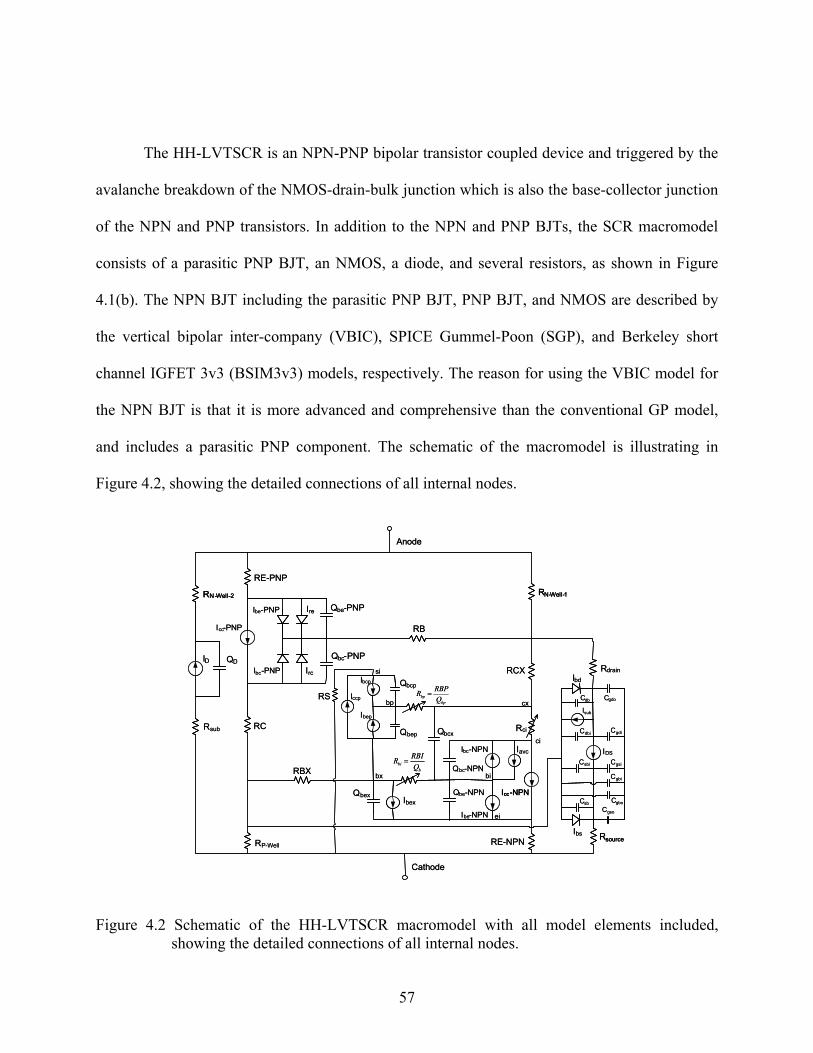
57
The HH-LVTSCR is an NPN-PNP bipolar transistor coupled device and triggered by the
avalanche breakdown of the NMOS-drain-bulk junction which is also the base-collector junction
of the NPN and PNP transistors. In addition to the NPN and PNP BJTs, the SCR macromodel
consists of a parasitic PNP BJT, an NMOS, a diode, and several resistors, as shown in Figure
4.1(b). The NPN BJT including the parasitic PNP BJT, PNP BJT, and NMOS are described by
the vertical bipolar inter-company (VBIC), SPICE Gummel-Poon (SGP), and Berkeley short
channel IGFET 3v3 (BSIM3v3) models, respectively. The reason for using the VBIC model for
the NPN BJT is that it is more advanced and comprehensive than the conventional GP model,
and includes a parasitic PNP component. The schematic of the macromodel is illustrating in
Figure 4.2, showing the detailed connections of all internal nodes.
Rsource
ID QD
Cathode
Anode
RP-Well
Rsub
RB
Qbe-PNP
Qbc-PNP
RE-PNP
RE-NPN
RC Rci
RCX
RBX
Qbcp
Qbep
Ibc-NPN
Ibe-NPN
Iavc
Icc-PNP
Cgso
Cgdo
Cgbo
Isub
Qbc-NPN
Qbcx
RS
Qbe-NPN
Iccp
Ibep
Ibcp
Ibc-PNP
Ibe-PNP
Rdrain
Cgbi
IDS
Csb
Cdb
Cgsi
CgdiCdbi
Csbi
si
QbexIbex
bp
bx bi
ci
ei
cx
Ibd
Ibs
Ire
Irc
bpbp
RBPRQ
=
bib
RBIRQ
=
RN-Well-2 RN-Well -1
Icc-NPN
RsourceRsource
ID QD
Cathode
Anode
RP-Well
Rsub
RB
Qbe-PNP
Qbc-PNP
RE-PNP
RE-NPN
RC Rci
RCX
RBX
Qbcp
Qbep
Ibc-NPN
Ibe-NPN
Iavc
Icc-PNP
Cgso
Cgdo
Cgbo
Isub
Qbc-NPN
Qbcx
RS
Qbe-NPN
Iccp
Ibep
Ibcp
Ibc-PNP
Ibe-PNP
Rdrain
Cgbi
IDS
Csb
Cdb
Cgsi
CgdiCdbi
Csbi
si
QbexIbex
bp
bx bi
ci
ei
cx
Ibd
Ibs
Ire
Irc
bpbp
RBPRQ
=
bib
RBIRQ
=
RN-Well-2RN-Well-2 RN-Well -1RN-Well -1
Icc-NPNIccIcc-NPN
Figure 4.2 Schematic of the HH-LVTSCR macromodel with all model elements included, showing the detailed connections of all internal nodes.
58
4.2.2. Substrate Parasitic Modeling
The CDM testing requires that the substrate of the device under test is charged either
directly or indirectly to the specified voltage. One of the input or output pins is then grounded,
and the behavior of the device during the subsequent high current discharge determines its CDM
ESD robustness [24][25].
The terminal connection of the HH-LVTSCR is as Figure 4.1(a). If the substrate of the
SCR is positively charged and the anode is grounded, then the P-Substrate/N-Well junction is
forward biased and current flows through the forward biased junction. Since the Emitter-NPN
and P-Well terminals are also tied to the substrate, the current will also pass through the forward
biased P-Well/N-Well junction. Additionally, the Emitter-NPN/P-Well junction is being reverse-
biased and the NPN transistor can be turned on. The discharge current flows both laterally and
vertically. On the other hand, if the device is negatively charged and the anode is grounded, the
HH-LVTSCR triggers in the normal manner, where the junction breakdown followed by the base
voltage raise of NPN and PNP transistors will result in the SCR being triggered [95].
Based on the above discussion, a diode, Dsub, is integrated into the macromodel
schematic to model the P-Substrate/N-Well junction (see Figure 4.1 ). In addition, P-Well, N-Epi
and P-Substrate also forms a substrate parasitic PNP transistor which has been included in the
VBIC NPN model. The VBIC model includes an intrinsic NPN transistor and a parasitic PNP
transistor. So no extra PNP transistor is needed to insert into the macromodel of Figure 4.1. This
is one advantage of using VBIC to model the NPN transistor.
59
4.2.3. Substrate Resistance Modeling
The important factors for SCR triggering are the substrate resistance RN-Well-1 and RP-Well
(see Figure 4.1). Before device triggering, the reverse saturation current of the blocking junction
mainly goes through these two resistances, as shown by dashed line in Figure 4.1(b). The current
level is very low. After device is triggered, appreciable current is injected into the N-Well and P-
Well from the terminal Emitter-PNP and Emitter-NPN to cause conductivity modulation. Little
current passes by RN-Well-1 and RP-Well. The current path is as dotted line in Figure 4.1(b). So the
resistance RN-Well-1 and RP-Well can be assumed to be constant independent of bias. There are
another two substrate resistances, RN-Well-2 and Rsub (Figure 4.1), which are associated with Dsub.
4.2.4. Negative Characteristic Modeling
The negative characteristic of the HH-LVTSCR is like a forward-biased diode, as the
TLP measurements in Figure 4.4. With the terminal connection as in Figure 4.1, when under the
reverse bias, the P-Well/N-Well and P-Substrate/N-Well junction diodes are forward biased and
diode-mode conduction results. The P-Substrate/N-Well junction has been modeled by Dsub. The
current path going through Dsub under reverse bias is denoted as P1 in Figure 4.1(a). The P-
Well/N-Well junction is the base-collector junction of the PNP transistor as well as the NPN
transistor. It has been modeled within the respective SGP model and VBIC model. The current
path going through P-Well/N-Well junction diode under reverse bias is denoted as P2 in Figure
4.1(a). There is one more current path going through the base-collector junction of the Parasitic-
PNP transistor built in VBIC, denoted as P3.
60
The SGP model is normally sufficiently accurate for the PNP BJT. We have found that, if
the GP model is used for the NPN transistor, which means there are only current path P1 and P2,
the simulation results can not fit the TLP measurement results since the coupled PNP and NPN
transistor models can not function correctly as a forward biased diode under reverse bias. If we
add an extra diode parallel with Dsub to fit the negative characteristic of the device, the added
diode will double-model the P-Well/N-Well junction and the positive characteristic of the
macromodel will be affected.
With the built-in parasitic PNP transistor, we have additional current path, P3, parallel
with P1 and P2 to conduct more reverse current. The VBIC model parameters, RS, RBP and
RCX (see Figure 4.2) can be tweaked to make the model to fit the negative characteristic.
4.2.5. Avalanche Current Modeling
The avalanche breakdown mechanism controls the SCR triggering and SCR conduction
after the snapback. In the conventional approach in which a SCR is modeled with two coupled
PNP and NPN bipolar transistors using the SGP model, an avalanche generation current source
has to be inserted in parallel with the base-collector junction, which is the N+/P-Well junction in
Figure 4.1(a), to properly characterize the junction breakdown [89]-[90]. A classical expression
for such a current source IBRK is given by [96]:
( )1( 1)
1BRK F n
BC BRK
I IV V
= ⋅ −− (4.1)
VBRK is the breakdown voltage of the base-collector junction, VBC is the voltage drop across this
junction, IF is the leakage current, and n is typically equal to 2. However, behavior languages or
61
special setups in CAD simulators are needed to implement such a current source, which could
significantly lower the simulation speed and may cause convergence problems.
Our approach of integrating the VBIC and BSIM models has alleviated this shortcoming,
as all the necessary avalanche current sources are imbedded in the equivalent circuit in Figure
4.2 [98]. In BSIM3v3 model, the substrate current Isub is given by [97]-[98].
0 01( )( ) expsub ds dseff dsa
eff ds dseff
I V V IL V Vα βα
⎛ ⎞= + − −⎜ ⎟⎜ ⎟−⎝ ⎠ (4.2)
Where Leff is the effective channel length of the MOS, Vdseff is the effective drain-source voltage,
Vdsat is in the saturation drain-source voltage, Idsa is the drain current without considering impact
ionization, and α0, α1 and β0 are fitting parameters associated with impact ionization coefficients
and Isub scalability. The avalanche current of the base-collector junction of the BJT is available in
the VBIC model given by [99]-[100]:
( )12( ) 1MC
lAVC Vcc bc laveI I I AVC V e
−− ⋅= − ⋅ ⋅ ⋅ (4.3)
21 ( ) 0.01 ( )2l bci bciV PC V PC V⎡ ⎤= − + + −⎣ ⎦ (4.4)
where Icc is the forward transport current, Ibc is the base/collector current shown as Icc-NPN and
Ibc-NPN current sources in Figure 4.2, (Icc - Ibc) is the collector current without avalanche, PC is
the junction built-in potential, MC is the junction grading coefficient, Vbci is the intrinsic voltage
drop over the junction, and AVC1 and AVC2 are fitting parameters.
These two parallel current sources in Equation (4.2) and Equation (4.3) correctly model
the avalanche generation current during the device triggering. In addition, they have similar
exponential voltage dependence and provide more fitting parameters to work with than using the
62
current source in Equation (4.1), which offer more control on the avalanche current to model the
snapback accurately. Moreover, without the need of any external current source, the
implementation of the macromodel is much simpler. In principle, the macromodel in Figure 4.2
can be implemented in any circuit simulator containing advanced MOS and BJT models. The
simplicity of this modeling approach offers advantages of higher simulation speed, more
flexibility, and less convergence issues.
4.2.6. High-Level Injection Modeling
After the device is triggered, considerable electrons and holes are injected from the
emitters of NPN and PNP transistor, and the SCR resistance is reduced significantly. The high-
level injection can also give rise to base pushout and conductivity modulation in the collector.
This effect is accounted for in the VBIC model with the quasi-saturation components. The quasi
saturation behavior is modeled with the resistor element Rci and charge elements Qbc and Qbcx
(see Figure 4.2). The quasi-saturation model consists of the current in the intrinsic collector
region (N-Epi region in Figure 4.1):
0
1ln1
bcirci bci bci
bciepi
KkTV K Kq K
IRCI
⎡ ⎤⎛ ⎞++ ⋅ − −⎢ ⎥⎜ ⎟+⎝ ⎠⎣ ⎦=
(4.5)
1 bciqV kTbciK GAMM e= + ⋅ (4.6)
1 bcxqV kTbcxK GAMM e= + ⋅ (4.7)
rci bci bcxV V V= − (4.8)
63
RCI is the intrinsic collector resistance, GAMM is the epi doping parameter, and Vbci and Vbcx are
equal to Vbi - Vci and Vbi - Vcx, respectively. The intrinsic collector resistance Rci is not formulated
explicitly. Instead, the current Irci passing through Rci is expressed as [99]-[100]:
( )
2
1 221
0.5 0.01
epiorci
epio
rci
II
I RCI
VVO
HRCF
=⎛ ⎞⎜ ⎟
⋅⎜ ⎟+ ⎜ ⎟⋅ +⎜ ⎟+⎜ ⎟⎝ ⎠ (4.9)
where VO is the epi drift saturation voltage and HRCF is the high current factor.
4.2.7. Capacitance Modeling
The principal dynamic behavior of the device is modeled by both the non-linear junction
and diffusion capacitances. Correctly modeling those capacitances is important to make the
SPICE simulation results predictable when running the transient simulation for the complete I/O
circuit. This is especially crucial when the transient stress is CDM.
As shown in Figure 4.2, there are a bunch of capacitances within the macromodel. They
have been modeled respectively by VBIC, SGP and BSIM3v3 and the associated model
parameters are extracted through the standard extraction process of each model, but the correct
“coupling” between the different capacitances has to be decided.
The base-emitter and base-collector junction charges of the PNP transistor are modeled
by Qbe-PNP and Qbc-PNP in the SGP model (see Figure 4.2). The parasitic capacitance of the
base-substrate junction is taken care of by QD in the diode component Dsub, and all the model
parameters associated with the base-substrate capacitance in the SGP model are set to zero.
64
In the VBIC NPN transistor model, the base-emitter and base-collector dielectric overlap
capacitances, CBEO and CBCO, originated from the double-poly BJT process, which is not
applicable for the NPN transistor considered here. So these capacitances are set to zero. The
base-emitter and base-collector junction charges are modeled by the intrinsic and extrinsic
portions which are Qbe-NPN and Qbex, and Qbc-NPN and Qbcx, respectively (see Figure 4.2). The
PNP transistor and the NPN transistor share the same base-collector junction, so the base-
collector junction charge should not be modeled twice by the VBIC and SGP models. Since the
VBIC has more advanced base-collector capacitance model than the SGP, we keep the initially
extracted model parameters for Qbc-NPN and Qbcx the same, but set the model parameter CJC in
the GP model to a very small value, say 0.1% of the original value. Qbc-NPN and Qbcx in VBIC
are given by [99]-[100]:
bc jc tri bciQ Q TR I QCO K= + ⋅ + ⋅ (4.10)
bcx bcxQ QCO K= ⋅ (4.11)
Qjc is the depletion charge and TR*Itri is the diffusion charge where TR is the reverse transit time
and Itri is the reverse transport current. The terms of QCO*Kbci and QCO*Kbcx are not included in
the SGP model and are used to describe the charge associated with the effect of high level
injection, a dominant mechanism after the SCR device is triggered.
BSIM3v3 also has the sophisticated capacitance models as illustrated in Figure 4.2 [97]-
[98]. All the model parameters associated with capacitances are kept the original extracted value
in order to get the correct transient response of the generation current.
65
4.2.8. Parameter Extraction
Contacts for all the seven terminals, N-Well, Emitter-PNP, Drain, Gate, Emitter-NPN, P-
Well and Substrate are made in order to carry out parameter extractions. Different terminals are
used and biased for the parametric tests of different models, as illustrated in Figure 4.3. Industry
standard software tool Integrated Circuit Characterization and Analysis Program (IC-CAP) is
used for the parameter extraction of VBIC, SGP and BSIM3v3. The model parameters are
extracted from the I-V and C-V characteristics measured by parameter analyzer with following
the standard model extraction strategies in IC-CAP user manual and BSIM3v3 user manual [97],
[101]-[103]. Special emphasis has been placed on the substrate current and the avalanche
breakdown current. The parameters associated with the generation current, α0, α1 and β0 in
BSIM3v3 as well as AVC1 and AVC2 in VBIC, are first extracted following the respective
standard algorithm. Based on the forward output I-V characteristics in avalanche breakdown
region (at high Vce), we can carry out the extraction and optimization of the parameter AVC1 and
AVC2. Then the two parameters are optimized to fit the curve of Ic/g0 versus Vce. Subsequently,
the above 5 fitting parameters are tweaked slightly to fit the measured snapback curves. An
advantage of the macromodeling approach, especially for industry applications, is that it allows
reusing of the already available accurate lumped models and parameter extraction for the non-
ESD domain of device operation.
The parameter extraction of the parasitic PNP transistor was done concurrently during the
standard VBIC model parameter extraction. Dsub, it is not suitable to use the 7-terminal structure
in Figure 4.3 to do measurement for model extraction. However, P-Substrate/N-Well junction is
one of the most important elementary junctions for the process. Dsub composes the parasitic
66
portion of the macromodels of the most valid devices. So it normally has been modeled for the
standard devices by design a specific structure to extract the characterization of the P-
Substrate/N-Well junction. The parameters are available to be used for the presented SCR mode.
The VBIC model parameters, RS, RBP and RCX (see Figure 4.2) will be tweaked to
make the model to fit the ESD conduction in the negative direction.
The value of RP-Well can be extracted from the forward-bias slope of the diode curve
obtained by grounding the Drain and Emitter-NPN terminals and biasing the P-Well terminal.
For extraction of RN-Well-1, the MEDICI TCAD tool is employed to calculate the sheet resistance,
Rs, of the n-well segment of the SCR structure in Figure 4.1. The value of RN-Well-1 is equal to Rs
times the length-to-width ratio. The other two substrate resistances RN-Well-2 and Rsub (Figure 4.1),
which are associated with Dsub, can also be calculated by multiplication of the relevant sheet
resistance with the length-to-width ratio.
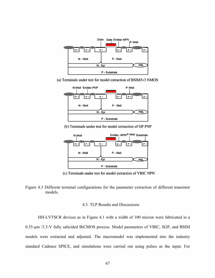
67
N - Well
P - Substrate
N - Epi
N-Well
Gate
P - Well
Drain
N + P +
Substrate
P-Well
N + N + P + P +
Emitter-PNP
Emitter-NPN
N - Well
P - Substrate
N - Epi
P - Well
N + P + N + N + P + P +
N - Well
P - Substrate
N - Epi
P - Well
N + P + N + N + P + P +
P-Well
P-WellEmitter -NPNN-Well
(a) Terminals under test for model extraction of BSIM3v3 NMOS
(b) Terminals under test for model extraction of GP PNP
(c) Terminals under test for model extraction of VBIC NPN
PBL
PBL
PBL
N - Well
P - Substrate
N - Epi
N-Well
Gate
P - Well
Drain
N + P +
Substrate
P-Well
N + N + P + P +
Emitter-PNP
Emitter-NPN
N - Well
P - Substrate
N - Epi
P - Well
N + P + N + N + P + P +
N - Well
P - Substrate
N - Epi
P - Well
N + P + N + N + P + P +
P-Well
P-WellEmitter -NPNN-Well
(a) Terminals under test for model extraction of BSIM3v3 NMOS
(b) Terminals under test for model extraction of GP PNP
(c) Terminals under test for model extraction of VBIC NPN
PBL
PBL
PBL
Figure 4.3 Different terminal configurations for the parameter extraction of different transistor models.
4.3. TLP Results and Discussions
HH-LVTSCR devices as in Figure 4.1 with a width of 100 micron were fabricated in a
0.35-μm /3.3-V fully salicided BiCMOS process. Model parameters of VBIC, SGP, and BSIM
models were extracted and adjusted. The macromodel was implemented into the industry
standard Cadence SPICE, and simulations were carried out using pulses as the input. For

68
measurement, Barth-4002 TLP pulse generator was used, and the rise time and width of TLP
pulses were 8 ns and 100 ns, respectively. The same pulses were also considered in simulations.
In Figure 4.4, an excellent match between the measured and simulated TLP I-V
characteristic is obtained for both the forward and reverse directions. In the positive direction,
the SCR triggers at 9.4 V and holds at 5 V, while the SCR turns on at 0.7 V and without
snapback in the reverse direction. Figure 4.4 also shows the simulation result of the macromodel
presented by Zhou et al. [92] with using the same model parameter set and the same setup of
simulation deck as the presented SCR maromodel. In Zhou et al.’s model, the substrate terminal
of the BJT is tied high to form the Anode of the SCR. Without adding a PNP transistor in his
macromodel, Zhou et al. just used the parasitic PNP and the intrinsic NPN transistors to form the
SCR. But VBIC model does not include a complete gummel-poon transistor for the parasitic
PNP. The parasitic transport current Iccp (Figure 4.2) models the substrate current when the
intrinsic transistor goes into saturation. It is given by [99]-[100]:
( )tfp trpccp
bp
I II
Q−
= (4.12)
( ) ( ) ( )( ) ( )1 1 1bep bciV NFP vt V NFP vttfpI WSP ISP e WSP ISP e⋅ ⋅= ⋅ ⋅ − + − ⋅ ⋅ −
(4.13)
( )( ) 1bcpV NFP vttrpI ISP e ⋅= ⋅ −
(4.14)
( )21 1 1 42bp pQ Q= + +
(4.15)
2tfp
p
IQ
IKP=
(4.16)
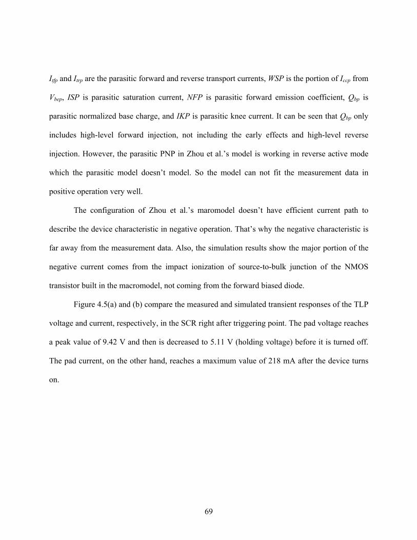
69
Itfp and Itrp are the parasitic forward and reverse transport currents, WSP is the portion of Iccp from
Vbep, ISP is parasitic saturation current, NFP is parasitic forward emission coefficient, Qbp is
parasitic normalized base charge, and IKP is parasitic knee current. It can be seen that Qbp only
includes high-level forward injection, not including the early effects and high-level reverse
injection. However, the parasitic PNP in Zhou et al.’s model is working in reverse active mode
which the parasitic model doesn’t model. So the model can not fit the measurement data in
positive operation very well.
The configuration of Zhou et al.’s maromodel doesn’t have efficient current path to
describe the device characteristic in negative operation. That’s why the negative characteristic is
far away from the measurement data. Also, the simulation results show the major portion of the
negative current comes from the impact ionization of source-to-bulk junction of the NMOS
transistor built in the macromodel, not coming from the forward biased diode.
Figure 4.5(a) and (b) compare the measured and simulated transient responses of the TLP
voltage and current, respectively, in the SCR right after triggering point. The pad voltage reaches
a peak value of 9.42 V and then is decreased to 5.11 V (holding voltage) before it is turned off.
The pad current, on the other hand, reaches a maximum value of 218 mA after the device turns
on.
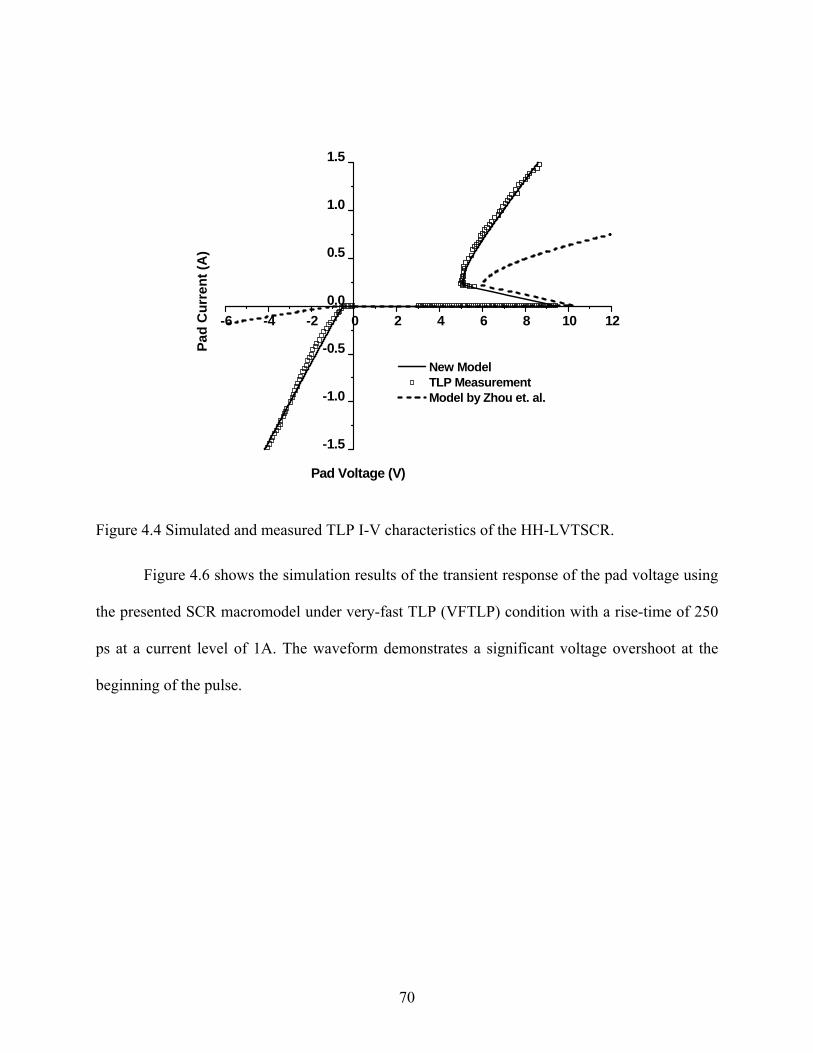
70
-6 -4 -2 0 2 4 6 8 10 12
-1.5
-1.0
-0.5
0.0
0.5
1.0
1.5
Pad
Cur
rent
(A)
Pad Voltage (V)
New Model TLP Measurement Model by Zhou et. al.
Figure 4.4 Simulated and measured TLP I-V characteristics of the HH-LVTSCR.
Figure 4.6 shows the simulation results of the transient response of the pad voltage using
the presented SCR macromodel under very-fast TLP (VFTLP) condition with a rise-time of 250
ps at a current level of 1A. The waveform demonstrates a significant voltage overshoot at the
beginning of the pulse.
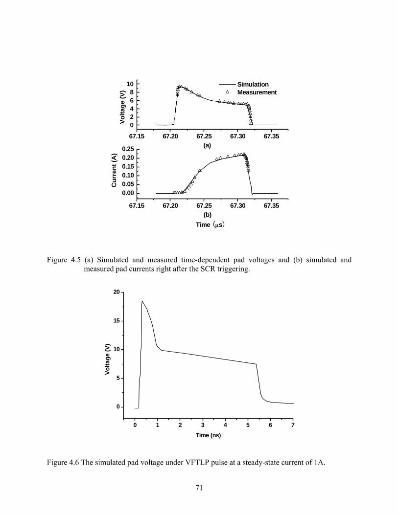
71
67.15 67.20 67.25 67.30 67.35
02468
10
67.15 67.20 67.25 67.30 67.35
0.000.050.100.150.200.25
(b)
(a)
Volta
ge (V
)
Time (μs)
C
urre
nt (A
)
Simulation Measurement
Figure 4.5 (a) Simulated and measured time-dependent pad voltages and (b) simulated and measured pad currents right after the SCR triggering.
0 1 2 3 4 5 6 7
0
5
10
15
20
Volta
ge (V
)
Time (ns)
Figure 4.6 The simulated pad voltage under VFTLP pulse at a steady-state current of 1A.
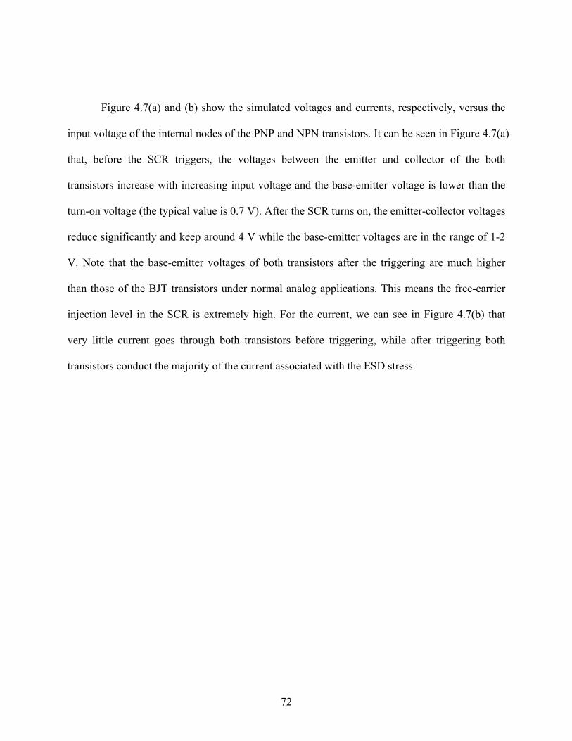
72
Figure 4.7(a) and (b) show the simulated voltages and currents, respectively, versus the
input voltage of the internal nodes of the PNP and NPN transistors. It can be seen in Figure 4.7(a)
that, before the SCR triggers, the voltages between the emitter and collector of the both
transistors increase with increasing input voltage and the base-emitter voltage is lower than the
turn-on voltage (the typical value is 0.7 V). After the SCR turns on, the emitter-collector voltages
reduce significantly and keep around 4 V while the base-emitter voltages are in the range of 1-2
V. Note that the base-emitter voltages of both transistors after the triggering are much higher
than those of the BJT transistors under normal analog applications. This means the free-carrier
injection level in the SCR is extremely high. For the current, we can see in Figure 4.7(b) that
very little current goes through both transistors before triggering, while after triggering both
transistors conduct the majority of the current associated with the ESD stress.

73
0 5 10 15 20-0.8
-0.6
-0.4
-0.2
0.0
0.2
0.4
0.6
0.8
0 5 10 15 20
0
2
4
6
8
10
12
(b)
(a)
Cur
rent
(A)
Anode to Cathode Voltage (V)
NPN-IB NPN-IC NPN-IE PNP-IB PNP-IC PNP-IE
Volta
ge (V
)
Anode to Cathode Voltage (V)
NPN-Vbe
NPN-Vce
PNP-Veb
PNP-Vec
Figure 4.7 Simulated (a) base-emitter and collector-emitter voltages of the PNP and NPN transistors and (b) emitter, base and collector currents of the PNP and NPN transistors.
4.4. CDM Transient Simulation of I/O Circuit
4.4.1. CDM Pulse Circuit
The CDM event can be emulated using the equivalent circuit in Figure 4.8 consisting of a
capacitance, inductance, resistance, and a JEDEC-specified small target made of a piece of metal
with a resistance of about 45 ohm. The current waveform associated with the CDM discharge
process depends on the values of the RLC and the charging voltage. In order to comply with the
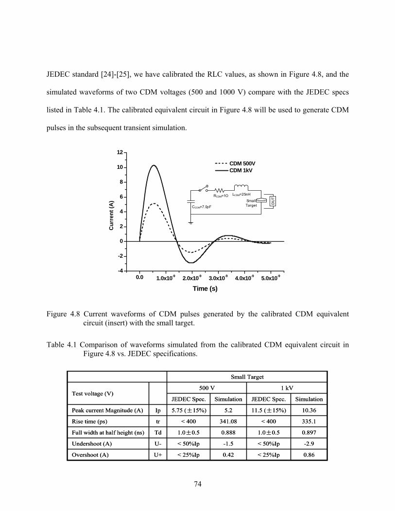
74
JEDEC standard [24]-[25], we have calibrated the RLC values, as shown in Figure 4.8, and the
simulated waveforms of two CDM voltages (500 and 1000 V) compare with the JEDEC specs
listed in Table 4.1. The calibrated equivalent circuit in Figure 4.8 will be used to generate CDM
pulses in the subsequent transient simulation.
0.0 1.0x10⁻⁹ 2.0x10⁻⁹ 3.0x10⁻⁹ 4.0x10⁻⁹ 5.0x10⁻⁹-4
-2
0
2
4
6
8
10
12
Small Target D
UT
CCDM=7.0pF
RCDM=1O LCDM=25nH
Cur
rent
(A)
Time (s)
CDM 500V CDM 1kV
Figure 4.8 Current waveforms of CDM pulses generated by the calibrated CDM equivalent circuit (insert) with the small target.
Table 4.1 Comparison of waveforms simulated from the calibrated CDM equivalent circuit in Figure 4.8 vs. JEDEC specifications.
0.86< 25%Ip0.42< 25%IpU+Overshoot (A)
-2.9< 50%Ip-1.5< 50%IpU-Undershoot (A)
0.8971.0±0.50.8881.0±0.5TdFull width at half height (ns)
335.1< 400341.08< 400trRise time (ps)
10.3611.5 (±15%)5.25.75 (±15%)IpPeak current Magnitude (A)
SimulationJEDEC Spec.SimulationJEDEC Spec.
1 kV500 VTest voltage (V)
Small Target
75
4.4.2. Experimental Results
The HH-LVTSCR devices with a width of 100 micron were integrated into a single pole
double throw (SPDT) analog switch. Figure 4.9(a) shows its on-chip ESD protection scheme.
The anode terminals of the SCR devices are all connected to the pads and their cathode terminals
are all connected to the common ground bus of the chip. The die size of the test chip is 1000*800
μm2, and its package type is 10-lead MicroPAK.
Figure 4.9(b) is the equivalent circuit schematic diagram of the layout showed in (a). In
the SPDT analog switch, there are three types of pins: input-only pins, output-only pins and
power supply pins. The ESD protection is provided by the SCR devices conducting current from
pins to ground bus, which is VSS-based ESD protection scheme as shown in Figure 1.8. Figure
4.9(b) illustrates the discharging paths under the JEDEC-standard CDM zaps. The diode inside
each SCR cell and the output NMOS denotes the device when it is working in the negative
operation.
SPDT analog switch parts are stressed by Thermo KeyTek RCDM automatic tester from
250 V to 1 kV. The stress method is compliance with JEDEC standard [24]-[25]. Those parts are
screened for pin leakage and functionality by automatic test equipment (ATE) before and after
CDM zaps to identify the failure voltage level. The test results revealed that, with the SCR
protecting devices at the pin, the input pins will fail after 500 V CDM zap and the SCR devices
can protect output pins up to 1 kV CDM.
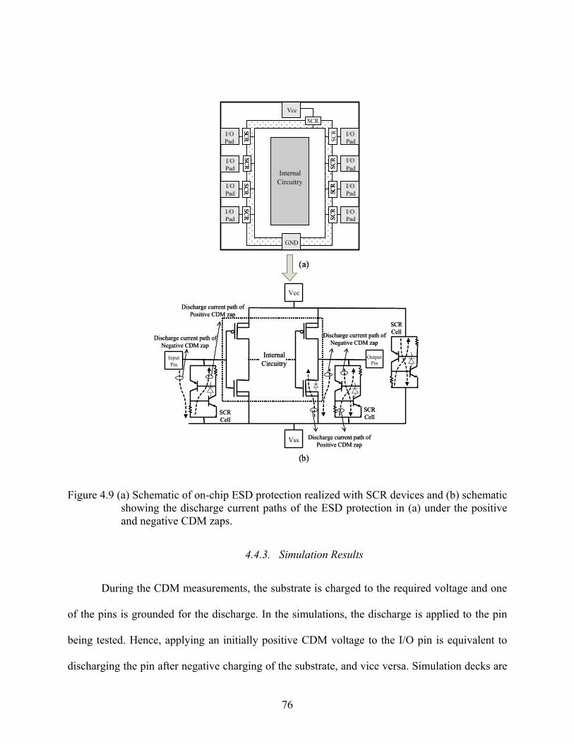
76
SCR
SCR
Internal Circuitry
SCR
SCR
S CRSCR
SCRS CR
I/O Pad
I/O Pad
I/O Pad
I/O Pad
Vcc
GND
Internal Circuitry
Input Pin
OutputPin
Vcc
Vss
SCR Cell
SCR Cell
SCR Cell
Discharge current path ofPositive CDM zap
SCR
I/O Pad
I/O Pad
I/O Pad
I/O Pad
Discharge current path ofNegative CDM zap
Discharge current path ofNegative CDM zap
Discharge current path ofPositive CDM zap
(a)
(b)
SCR
SCR
SCR
Internal Circuitry
SCR
SCR
SCR
SCR
S CRS CR
SCRSCR
SCRSCR
S CRS CR
I/O Pad
I/O Pad
I/O Pad
I/O Pad
Vcc
GND
Internal Circuitry
Input Pin
OutputPin
Vcc
Vss
SCR Cell
SCR Cell
SCR Cell
Discharge current path ofPositive CDM zap
SCR
I/O Pad
I/O Pad
I/O Pad
I/O Pad
Discharge current path ofNegative CDM zap
Discharge current path ofNegative CDM zap
Discharge current path ofPositive CDM zap
(a)
(b)
Figure 4.9 (a) Schematic of on-chip ESD protection realized with SCR devices and (b) schematic showing the discharge current paths of the ESD protection in (a) under the positive and negative CDM zaps.
4.4.3. Simulation Results
During the CDM measurements, the substrate is charged to the required voltage and one
of the pins is grounded for the discharge. In the simulations, the discharge is applied to the pin
being tested. Hence, applying an initially positive CDM voltage to the I/O pin is equivalent to
discharging the pin after negative charging of the substrate, and vice versa. Simulation decks are
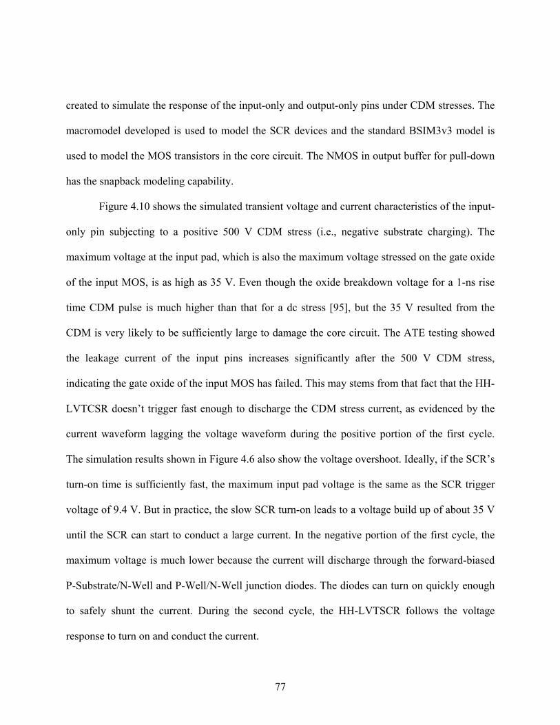
77
created to simulate the response of the input-only and output-only pins under CDM stresses. The
macromodel developed is used to model the SCR devices and the standard BSIM3v3 model is
used to model the MOS transistors in the core circuit. The NMOS in output buffer for pull-down
has the snapback modeling capability.
Figure 4.10 shows the simulated transient voltage and current characteristics of the input-
only pin subjecting to a positive 500 V CDM stress (i.e., negative substrate charging). The
maximum voltage at the input pad, which is also the maximum voltage stressed on the gate oxide
of the input MOS, is as high as 35 V. Even though the oxide breakdown voltage for a 1-ns rise
time CDM pulse is much higher than that for a dc stress [95], but the 35 V resulted from the
CDM is very likely to be sufficiently large to damage the core circuit. The ATE testing showed
the leakage current of the input pins increases significantly after the 500 V CDM stress,
indicating the gate oxide of the input MOS has failed. This may stems from that fact that the HH-
LVTCSR doesn’t trigger fast enough to discharge the CDM stress current, as evidenced by the
current waveform lagging the voltage waveform during the positive portion of the first cycle.
The simulation results shown in Figure 4.6 also show the voltage overshoot. Ideally, if the SCR’s
turn-on time is sufficiently fast, the maximum input pad voltage is the same as the SCR trigger
voltage of 9.4 V. But in practice, the slow SCR turn-on leads to a voltage build up of about 35 V
until the SCR can start to conduct a large current. In the negative portion of the first cycle, the
maximum voltage is much lower because the current will discharge through the forward-biased
P-Substrate/N-Well and P-Well/N-Well junction diodes. The diodes can turn on quickly enough
to safely shunt the current. During the second cycle, the HH-LVTSCR follows the voltage
response to turn on and conduct the current.
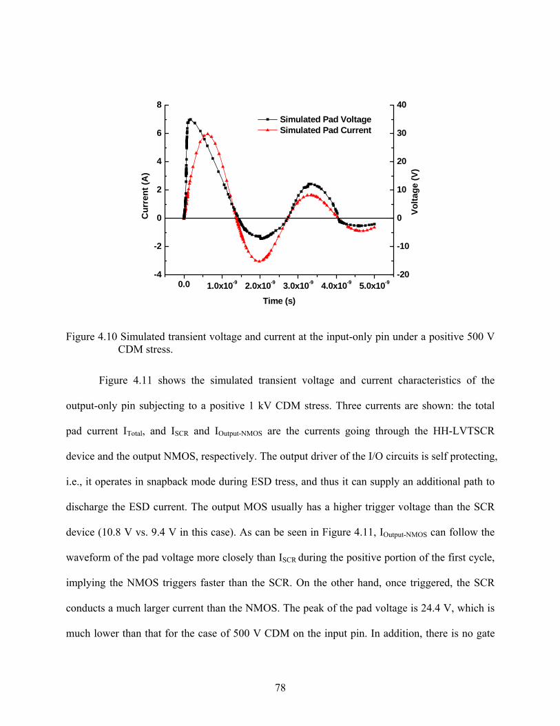
78
0.0 1.0x10⁻⁹ 2.0x10⁻⁹ 3.0x10⁻⁹ 4.0x10⁻⁹ 5.0x10⁻⁹-4
-2
0
2
4
6
8
-20
-10
0
10
20
30
40
Volta
ge (V
)
Cur
rent
(A)
Time (s)
Simulated Pad Voltage Simulated Pad Current
Figure 4.10 Simulated transient voltage and current at the input-only pin under a positive 500 V CDM stress.
Figure 4.11 shows the simulated transient voltage and current characteristics of the
output-only pin subjecting to a positive 1 kV CDM stress. Three currents are shown: the total
pad current ITotal, and ISCR and IOutput-NMOS are the currents going through the HH-LVTSCR
device and the output NMOS, respectively. The output driver of the I/O circuits is self protecting,
i.e., it operates in snapback mode during ESD tress, and thus it can supply an additional path to
discharge the ESD current. The output MOS usually has a higher trigger voltage than the SCR
device (10.8 V vs. 9.4 V in this case). As can be seen in Figure 4.11, IOutput-NMOS can follow the
waveform of the pad voltage more closely than ISCR during the positive portion of the first cycle,
implying the NMOS triggers faster than the SCR. On the other hand, once triggered, the SCR
conducts a much larger current than the NMOS. The peak of the pad voltage is 24.4 V, which is
much lower than that for the case of 500 V CDM on the input pin. In addition, there is no gate
79
oxide directly subjecting the ESD stress in the case of the output-only pin. As such, the CDM
robustness of the output pin is higher than that of the input pin. During the negative portion,
IOutput-NMOS will go through the forward-biased p-well/drain junction diode.
0.0 1.0x10⁻⁹ 2.0x10⁻⁹ 3.0x10⁻⁹ 4.0x10⁻⁹ 5.0x10⁻⁹-8-6-4-202468
10121416
-15
-10
-5
0
5
10
15
20
25
30
Volta
ge (V
)
Cur
rent
(A)
Time (s)
Simulated Pad Voltage ITotal
ISCR
IOutput-NMOS
Figure 4.11 Simulated transient voltage and currents at the output-only pin under a positive 1 kV CDM stress.
The above simulation finding is consistent with the testing results that the input pins
failed after a 500 V CDM stress and the output pins failed at a higher level of 1 kV CDM. While
the output NMOS is self-protecting, the ESD protection device, like HH-LVTSCR considered, is
still indispensable for the output pins. The total width of the output NMOS is not big enough to
handle all the ESD current (the total width of the output NMOS in this presented case is 40 μm)
and its area efficiency of ESD protection is lower than that of the SCR protection device.
80
In order to improve the CDM robustness of the pins, a clear way is to reduce the pad
clamping voltage. A suggested way is to provide an alternate discharge path from pad to VSS or
to reduce the impedance of the existing path [104] or to design new ESD protection structures
which can trigger fast enough to offer adequate CDM protection.
Thus, the model developed, together with the knowledge of pad voltage that can be
applied to the I/O pin without damaging the core circuit, can be used to predict the I/O pin ESD
protection level offered by the SCR protection devices.
4.5. Chapter Summary
In this chapter, we have presented a comprehensive compact model of SCR for the
simulation of integrated circuits subjected to a pervasive ESD event called the charge device
model (CDM). The work illustrated the useful and effective macromodeling approach of
integrating the various industry standard models to describe the individual devices imbedded in
the SCR. In addition, the modeling of the avalanche current sources, substrate parastics, and
capacitances were discussed. The issue of parameter extraction was addressed as well. The
macromodel has been implemented into Cadence SPICE, and TLP and transient simulations
have been carried out. A 0.35-μm CMOS circuit subjecting to CDM stresses was also considered
and tested in support of the modeling development.
81
CHAPTER 5. COMPARISON OF VBIC AND CONVENTIONAL GUMMEL-POON MODEL FOR ESD SCR COMPACT MODELING
5.1. Introduction
In Chapter 4, we have already discussed how important to build a predictable compact
model for SCR devices for ESD protection design and what are the difficulties of building such
model. Also, Chapter 4 presents a marcomodeling approach to build an accurate, stable and fast
SCR compact model by taking the advantage of the advanced BJT model, VBIC. This modeling
approach offers simplicity, wide availability and compatibility with most commercial simulators.
In additional, this approach by using VBIC model can quickly adapted to technology scaling
when new physical phenomena is updated into standard VBIC model for the latest state-of-art
technologies by compact modeling community. Furthermore, the sophisticated capacitance
modeling and the parasitical PNP in the advanced VBIC model ensure this macromodel
approach can simulate the response of the SCR device to very fast transient stimulus such as
CDM.
The macromodeling approach is to use the existing device model to build an equivalent
sub-circuit to describe the characteristic of the device to be modeled. This approach is highly
suitable for modeling a device whose behavior is hard to describe with a close-form analytical
solutions. The SCR device is a PNP-NPN transistor coupled system. The straightforward idea to
model this device is to consolidate a PNP and a NPN BJT to represent the SCR device. The
question is what kind of model should be used for the PNP and NPN transistors in SCR sub-
82
circuit model to make the model accurate. SPICE Gummel-Poon (SGP) model has served the ICs
industry well for over 20 years [105]-[106]. Some literatures have reported SCR sub-circuit
models by using SGP model for the PNP and NPN transistors inside the models [89][90], but the
models have to include the extra current/voltage source and the models can not describe the
negative operation state and the response of the SCR device under very fast transient event. The
SGP model is a three-terminal model and consists of three current sources, Icc, Ibc and Ibe, as
shown in Figure 5.1 which is a NPN-type model circuit. Irc and Ire are the recombination current
in base-collector depletion region and in base-emitter depletion region. The basic of all variants
of the SGP model is the integral charge control model for the dc current Icc passing through the
emitter and collector terminals. There are two capacitances, Qbc and Qbe, associated with the
charges stored between the base and collector terminals and between the base and emitter
terminals.
The Unlike the conventional SGP model, the VBIC is a four-terminal model comprising
the base, emitter, collector and substrate which includes several features that make it distinct
with the SGP model. Figure 5.2 shows the equivalent sub-circuit and complete model network of
a NPN-type VBIC model. The main modeling enhancements of VBIC over SGP are:
1. The improved early effect modeling. The early effect in VBIC models via q1
term to cover the bias dependence of output conductance over a wide range of
biases.
2. Quasi-saturation modeling, which models the conductivity modulation of the
collector.
83
3. Parasitic substrate transistor modeling. VBIC model composes a intrinsic
NPN transistor and a parasitic PNP transistor.
4. Parasitic oxide capacitance modeling.
5. Avalanche current modeling. VBIC models the base-collector avalanche
current at high reverse bias when the device is in forward-active mode.
6. Decoupling of base and collector current. In the conventional SGP model, the
base and collector currents are correlated with current gain while in VBIC
model, there is no such direct connection between the two currents.
7. Improved temperature dependence modeling.
8. Self heating modeling.
9. Capacitance continuous modeling.
For ESD compact modeling purpose, are all the above advanced features benefit the sub-
circuit model with using VBIC model to be a superior one and how these distinct features benefit
the SCR compact model for ESD application? This chapter seeks to compare the difference of
SCR compact model built by using VBIC and conventional SGP in order to point out the
important features of VBIC model for building an accurate and easy-CAD implement SCR
model and explain why from device physics and model theory perspectives. First, the
development of SCR macromodels by using VBIC and SGP will be presented. The results
calculated from the VBIC-based macromodel, calculated from SGP based macromodel and
obtained from measurements will be compared. This will be followed by the discussion of what
kind of unique features in VBIC model, comparing with SGP model, make the VBIC-based
macromodel model SCR triggering and characteristics in conduction mode accurately.
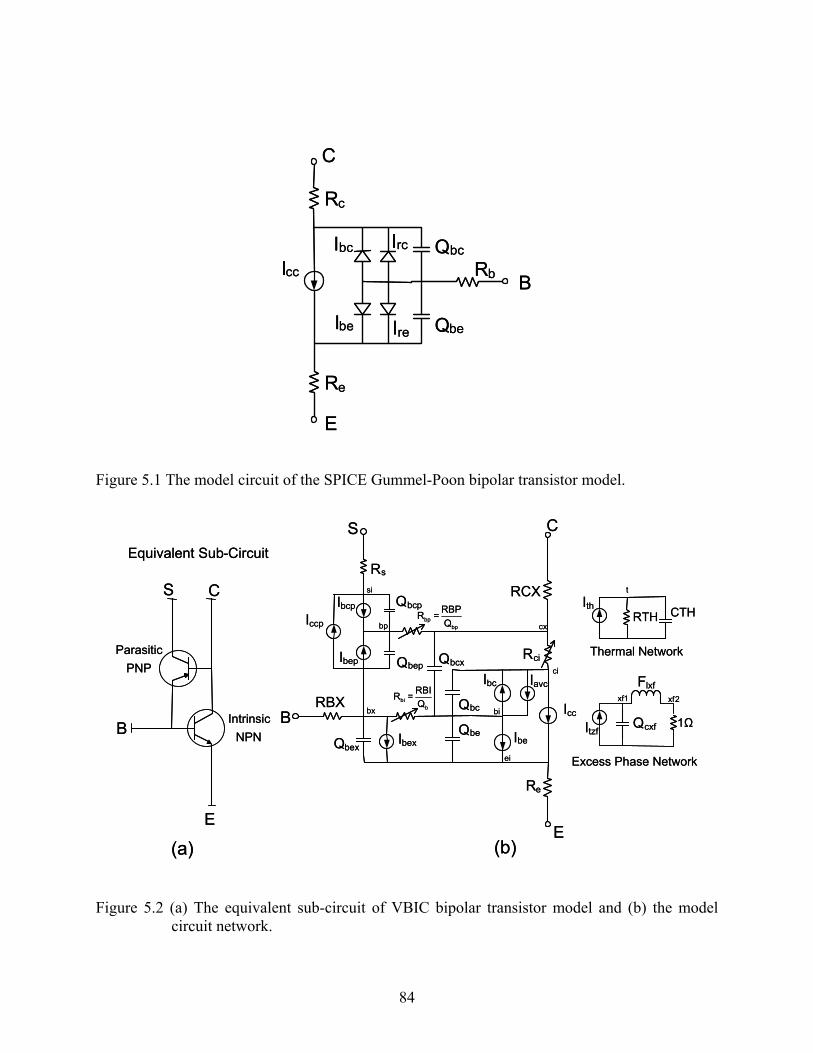
84
Rb
Qbe
Qbc
Re
Rc
Icc
Ibc
Ibe Ire
Irc
B
C
E
Rb
Qbe
Qbc
Re
Rc
Icc
Ibc
Ibe Ire
Irc
B
C
E
Figure 5.1 The model circuit of the SPICE Gummel-Poon bipolar transistor model.
Re
Rci
RCX
RBX
Qbcp
Qbep
Ibc
Ibe
Iavc
IccQbc
Qbcx
Rs
Qbe
Iccp
Ibep
Ibcp
si
QbexIbex
bp
bx bi
ci
ei
cx
B
C
E
S
CS
E
Intrinsic NPN
Parasitic PNP
Excess Phase Network
Thermal Network
Itzf
IthRTH CTH
Qcxf
Flxf
t
xf1 xf2
Equivalent Sub-Circuit
bib
RBIR =Q
1Ω
bpbp
RBPR =Q
(a) (b)
B
Re
Rci
RCX
RBX
Qbcp
Qbep
Ibc
Ibe
Iavc
IccQbc
Qbcx
Rs
Qbe
Iccp
Ibep
Ibcp
si
QbexIbex
bp
bx bi
ci
ei
cx
B
C
E
S
CS
E
Intrinsic NPN
Parasitic PNP
Excess Phase Network
Thermal Network
Itzf
IthRTH CTH
Qcxf
Flxf
t
xf1 xf2
Equivalent Sub-Circuit
bib
RBIR =Q
1Ω
bpbp
RBPR =Q
(a) (b)
B
Figure 5.2 (a) The equivalent sub-circuit of VBIC bipolar transistor model and (b) the model circuit network.
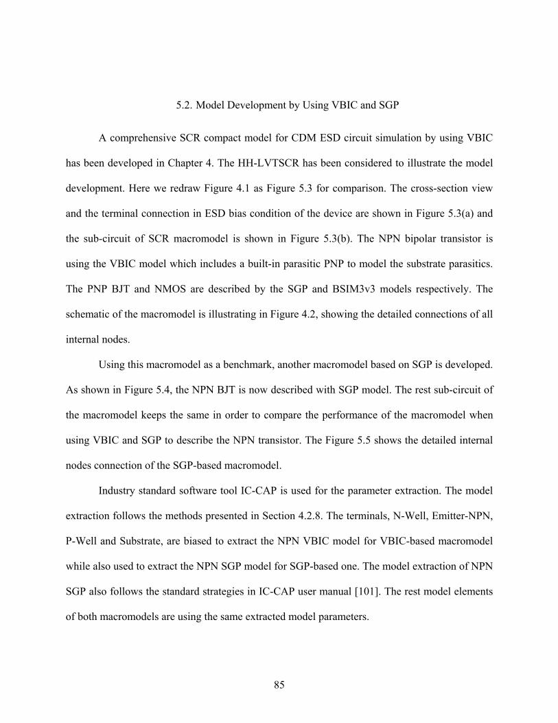
85
5.2. Model Development by Using VBIC and SGP
A comprehensive SCR compact model for CDM ESD circuit simulation by using VBIC
has been developed in Chapter 4. The HH-LVTSCR has been considered to illustrate the model
development. Here we redraw Figure 4.1 as Figure 5.3 for comparison. The cross-section view
and the terminal connection in ESD bias condition of the device are shown in Figure 5.3(a) and
the sub-circuit of SCR macromodel is shown in Figure 5.3(b). The NPN bipolar transistor is
using the VBIC model which includes a built-in parasitic PNP to model the substrate parasitics.
The PNP BJT and NMOS are described by the SGP and BSIM3v3 models respectively. The
schematic of the macromodel is illustrating in Figure 4.2, showing the detailed connections of all
internal nodes.
Using this macromodel as a benchmark, another macromodel based on SGP is developed.
As shown in Figure 5.4, the NPN BJT is now described with SGP model. The rest sub-circuit of
the macromodel keeps the same in order to compare the performance of the macromodel when
using VBIC and SGP to describe the NPN transistor. The Figure 5.5 shows the detailed internal
nodes connection of the SGP-based macromodel.
Industry standard software tool IC-CAP is used for the parameter extraction. The model
extraction follows the methods presented in Section 4.2.8. The terminals, N-Well, Emitter-NPN,
P-Well and Substrate, are biased to extract the NPN VBIC model for VBIC-based macromodel
while also used to extract the NPN SGP model for SGP-based one. The model extraction of NPN
SGP also follows the standard strategies in IC-CAP user manual [101]. The rest model elements
of both macromodels are using the same extracted model parameters.
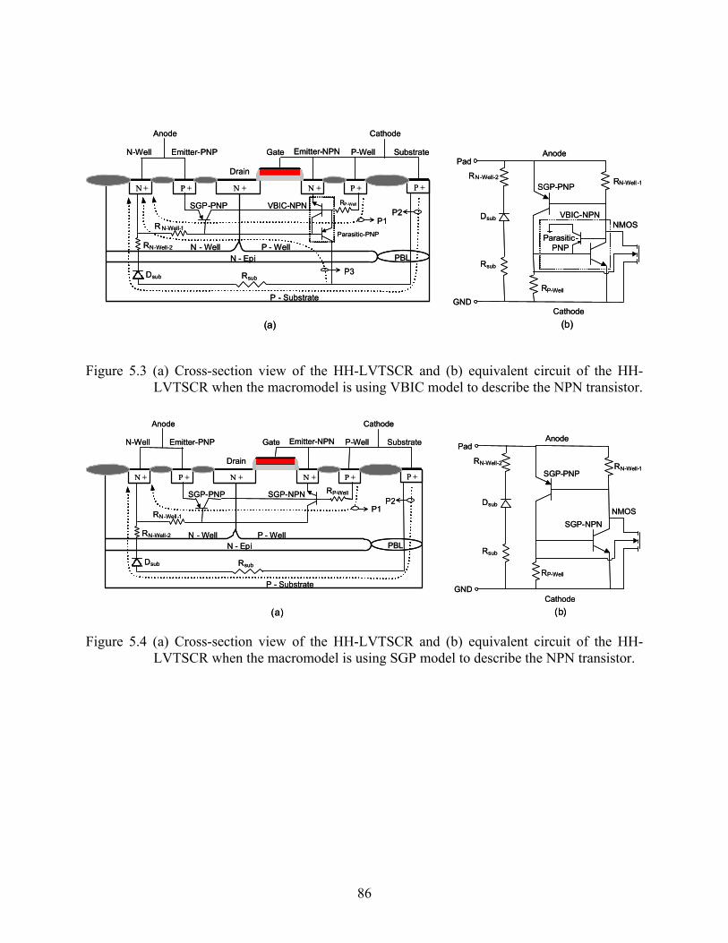
86
N - Well
P - Substrate
N - Epi
N-Well Gate
P - Well
Anode Cathode
Drain
N + P +
Substrate
RP-Well
Rsub
R N-Well-1
VBIC-NPNSGP-PNP
Dsub
P-Well
N + N + P + P +
Emitter-PNP Emitter-NPN
RN-Well-2
Parasitic-PNP
P1
P3
P2
PBL
Cathode
Anode
RN-Well -1
RP-Well
SGP-PNP
Parasitic-PNP
NMOSVBIC-NPN
RN-Well-2
Rsub
Dsub
GND
Pad
(a) (b)
Figure 5.3 (a) Cross-section view of the HH-LVTSCR and (b) equivalent circuit of the HH-LVTSCR when the macromodel is using VBIC model to describe the NPN transistor.
N - Well
P - Substrate
N - Epi
N-Well Gate
P - Well
Anode Cathode
Drain
N + P +
Substrate
RP-Well
Rsub
RN-Well-1
SGP-NPNSGP-PNP
Dsub
P-Well
N + N + P + P +
Emitter-PNP Emitter-NPN
RN-Well-2
P1P2
PBL
Cathode
Anode
RN-Well-1
RP-Well
SGP-PNP
NMOSSGP-NPN
RN-Well-2
Rsub
Dsub
GND
Pad
(a) (b)
N - Well
P - Substrate
N - Epi
N-Well Gate
P - Well
Anode Cathode
Drain
N + P +
Substrate
RP-Well
Rsub
RN-Well-1
SGP-NPNSGP-PNP
Dsub
P-Well
N + N + P + P +
Emitter-PNP Emitter-NPN
RN-Well-2
P1P2
PBL
Cathode
Anode
RN-Well-1
RP-Well
SGP-PNP
NMOSSGP-NPN
RN-Well-2
Rsub
Dsub
GND
Pad
(a) (b)
Figure 5.4 (a) Cross-section view of the HH-LVTSCR and (b) equivalent circuit of the HH-LVTSCR when the macromodel is using SGP model to describe the NPN transistor.

87
Rsource
ID QD
Cathode
Anode
RN-Well -1
RP-Well
RN-Well-2
Rsub
RB-PNP
Qbe-PNP
Qbc-PNP
RE-PNP
RE-NPN
RC-PNP
RC-NPN
RB-NPN
Icc-PNP
Cgso
Cgdo
Cgbo
Isub
Ibc-PNP
Ibe-PNP
Rdrain
Cgbi
IDS
Csb
Cdb
Cgsi
CgdiCdbi
Csbi
Ibd
Ibs
Irc-PNP
Icc-NPN
Ire-PNP
Qbe-NPN
Qbc-NPN Ibc-NPN
Ibe-NPN
Ire-NPN
Irc-NPN
Rsource
ID QD
Cathode
Anode
RN-Well -1
RP-Well
RN-Well-2
Rsub
RB-PNP
Qbe-PNP
Qbc-PNP
RE-PNP
RE-NPN
RC-PNP
RC-NPN
RB-NPN
Icc-PNP
Cgso
Cgdo
Cgbo
Isub
Ibc-PNP
Ibe-PNP
Rdrain
Cgbi
IDS
Csb
Cdb
Cgsi
CgdiCdbi
Csbi
Ibd
Ibs
Irc-PNP
Icc-NPN
Ire-PNP
Qbe-NPN
Qbc-NPN Ibc-NPN
Ibe-NPN
Ire-NPN
Irc-NPN
Figure 5.5 Schematic of the HH-LVTSCR SGP-based macromodel with all model elements included, showing the detailed connections of all internal nodes.
The two macromodel were implemented into the industry standard Cadence SPICE, and
simulations were carried out using pulses as the input. HH-LVTSCR devices with a width of 100
micron were fabricated in a 0.35-μm/3.3-V fully salicided BiCMOS process for model validation.
Barth-4002 TLP pulse generator was used to do the measurement, and the rise time and width of
TLP pulses were 8 ns and 100 ns, respectively. The same pulses were also considered in
simulations.
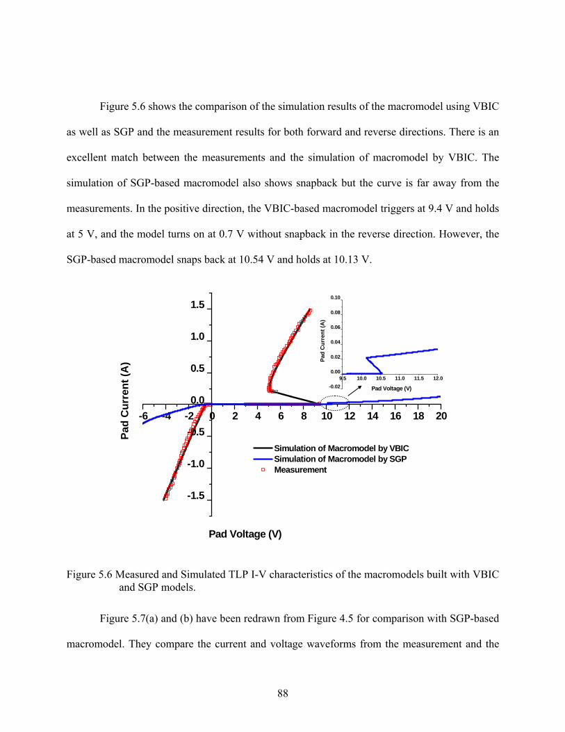
88
Figure 5.6 shows the comparison of the simulation results of the macromodel using VBIC
as well as SGP and the measurement results for both forward and reverse directions. There is an
excellent match between the measurements and the simulation of macromodel by VBIC. The
simulation of SGP-based macromodel also shows snapback but the curve is far away from the
measurements. In the positive direction, the VBIC-based macromodel triggers at 9.4 V and holds
at 5 V, and the model turns on at 0.7 V without snapback in the reverse direction. However, the
SGP-based macromodel snaps back at 10.54 V and holds at 10.13 V.
Figure 5.6 Measured and Simulated TLP I-V characteristics of the macromodels built with VBIC and SGP models.
Figure 5.7(a) and (b) have been redrawn from Figure 4.5 for comparison with SGP-based
macromodel. They compare the current and voltage waveforms from the measurement and the
-6 -4 -2 0 2 4 6 8 10 12 14 16 18 20
-1.5
-1.0
-0.5
0.0
0.5
1.0
1.5
9.5 10.0 10.5 11.0 11.5 12.0-0.02
0.00
0.02
0.04
0.06
0.08
0.10
Pad
Cur
rent
(A)
Pad Voltage (V)
Pad
Cur
rent
(A)
Pad Voltage (V)
Simulation of Macromodel by VBIC Simulation of Macromodel by SGP Measurement
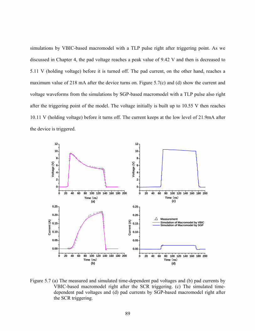
89
simulations by VBIC-based macromodel with a TLP pulse right after triggering point. As we
discussed in Chapter 4, the pad voltage reaches a peak value of 9.42 V and then is decreased to
5.11 V (holding voltage) before it is turned off. The pad current, on the other hand, reaches a
maximum value of 218 mA after the device turns on. Figure 5.7(c) and (d) show the current and
voltage waveforms from the simulations by SGP-based macromodel with a TLP pulse also right
after the triggering point of the model. The voltage initially is built up to 10.55 V then reaches
10.11 V (holding voltage) before it turns off. The current keeps at the low level of 21.9mA after
the device is triggered.
0 20 40 60 80 100 120 140 160 180 200
0
2
4
6
8
10
12
0 20 40 60 80 100 120 140 160 180 200
0.00
0.05
0.10
0.15
0.20
0.25
0 20 40 60 80 100 120 140 160 180 200
0
2
4
6
8
10
12
0 20 40 60 80 100 120 140 160 180 200
0.00
0.05
0.10
0.15
0.20
0.25
Measurement Simulation of Macromodel by VBIC
Time (ns)
Volta
ge (V
)
(d)(b)
(c)(a)
Time (ns)
Cur
rent
(A)
Simulation of Macromodel by SGP
Time (ns)
Volta
ge (V
)
C
urre
nt (A
)
Time (ns)
Figure 5.7 (a) The measured and simulated time-dependent pad voltages and (b) pad currents by VBIC-based macromodel right after the SCR triggering. (c) The simulated time-dependent pad voltages and (d) pad currents by SGP-based macromodel right after the SCR triggering.
90
5.3. Model Analysis and Discussion
5.3.1. Triggering Region
As shown in Figure 5.7, the SGP-based macromodel does not snapback correctly since
the macromodel doesn’t model correctly the avalanche breakdown current which is the most
important components to determine the device triggering.
We have discussed in Section 4.2.5 that in the conventional approach in which a SCR is
modeled with two coupled PNP and NPN bipolar transistors using the SGP model, an avalanche
generation current source as Equation (4.1) has to be inserted in parallel with the base-collector
junction to properly characterize the junction breakdown [89]-[90]. For the macromodel using
VBIC, no extra current source is needed. All the necessary avalanche current sources are
imbedded in the equivalent circuit in Figure 4.2, as described with Equation (4.2) and (4.3).
For the macromodel using SGP for NPN transistor, there is no avalanche breakdown
model in SGP. The macromodel only has one current source imbedded in NMOS transistor
described by BSIM3v3 (Equation (4.2)). Isub accounts for a big portion of the generation current
in VBIC-based macromodel, so the SGP-based macromodel dose snapback even with this one
current source. But without enough generation current generated by the model, the model will
not triggered at the right voltage. Also, the model doesn’t work out the right holding voltage.
Figure 3.3 shows the directions of all electron and hole currents after the SCR triggers which
means both PNP and NPN transistors turn on. Igen is avalanche generation current. The two
current sources, Iave (Equation (4.3)) and Isub (Equation (4.2)), compose Igen in the VBIC-based
macromodel while in the SGP-based macromodel, there is only Isub who functions as Igen. Igen is
given by Equation (3.1). As discussed in Section 3.2, after both PNP and NPN bipolar transistors

91
turn on, Igen will be described as Equation (3.2). Then the value of M will reduce and the voltage
at Anode drops to VH. The value of VH is dependent on the voltage at Anode required to maintain
the base to emitter voltage at the level needed to sustain the bipolar current. Hence, VH is a
function of RN-Well, RP-Well, RP, M and the gains of both intrinsic PNP and NPN transistors, βPNP
and βNPN. As shown in Figure 3.3,
H H P BC SUB PNP N Well SUB NPN P WellV I R V I R I R− − − −= ⋅ + + ⋅ + ⋅ (5.1)
1(1 )SUB PNP H C PNPPNP
I I Iβ− −= − ⋅ +
(5.2)
1(1 )SUB NPN H C NPNNPN
I I Iβ− −= − ⋅ +
(5.3)
Replacing equations (5.2) and (5.3) in equation (5.1), we will get
1 1( ) (1 ) (1 )H H P N Well P Well BC C PNP N Well C NPN P WellPNP NPN
V I R R R V I R I Rβ β− − − − − −= ⋅ + + + − ⋅ + − ⋅ +
(5.4)
IH, IC-PNP and IC-NPN are functions of βPNP and βNPN, and VBC, the voltage drop across base-
collector junction, determines how big M will be. Since the SGP-based maromodel has only one
current source, which requires higher VBC to reach higher M in order to get enough Igen. So the
model has not been able to hold at the right voltage. The VH is much higher for SGP-based
maromodel. The comparison results presented in Figure 5.7 shows that it is not efficient enough
to model the SCR triggering when having the only one current source, Isub in NMOS.
Extra current source needs to be added into the macromodel with NPN transistor
described by SGP. In this way, behavior languages or special setups in CAD simulators are
needed to implement such extra current source, which could significantly lower the simulation

92
speed and may cause convergence problems, while the implementation of the VBIC-based
macromodel is much simpler. In principle, the macromodel in Figure 4.2 can be implemented in
any circuit simulator containing advanced MOS and BJT models. The simplicity of this
modeling approach offers advantages of higher simulation speed, more flexibility, and less
convergence issues.
0 5 10 15 20
02468
10121416182022
0 5 10 15 20-0.6
-0.4
-0.2
0.0
0.2
0.4
0.6
Volta
ge (V
)
Anode to Cathode Voltage (V)
NPN-Vbe
NPN-Vce
PNP-Veb
PNP-Vec
(b)
(a)
Cur
rent
(A)
Anode to Cathode Voltage (V)
NPN-IB NPN-IC NPN-IE PNP-IB PNP-IC PNP-IE
Figure 5.8 Simulated (a) base-emitter and collector-emitter voltages of the PNP and NPN transistors and (b) emitter, base and collector currents of the PNP and NPN transistors in the SGP-based macromodel.
93
Comparing with Figure 4.7, Figure 5.8(a) and (b) show the simulated voltages and
currents, respectively, versus the input voltage of the internal nodes of the PNP and NPN
transistors for the SGP-based macromodel. In Figure 5.8(a), the emitter-collector voltages of
both transistors also increase with increasing input voltage. The trigger voltage of the
macromodel by SGP model is higher than that of the one by VBIC model. After the SCR turns
on, the emitter-collector voltages reduce little bit and keep increasing afterwards while the base-
emitter voltages are in the range of 0.8-1.0 V. For the currents in Figure 5.8(b), very little current
goes through both transistors before triggering, while after triggering the current conduction
level of both transistors are low.
5.3.2. High Current Region
After the SCR device enters conduction mode, both PNP and NPN transistor turn on and
work in forward active mode. The simulated shape of I-V curve in conducting state depends on
the current level both PNP and NPN transistor models can work out. As shown in Figure 5.6,
Figure 4.7 and Figure 5.8, the conduction current level of SGP-based macromodel is low after
the model turns on while the VBIC-based macromodel can give the accurate conduction current.
After the device is triggered, considerable electrons and holes are injected from the
emitters of NPN and PNP transistor, and the SCR resistance is reduced significantly. As shown
in Figure 4.7 and Figure 5.8, the base-emitter biases of PNP and NPN transistors in both
macromodels are higher than those of the BJT transistors under normal analog applications,
especially the biases in the VBIC-based macromodel. This means the free-carrier injection level
in the SCR is extremely high. The high-level injection can also give rise to base pushout and
94
conductivity modulation in the collector. This effect is accounted for in the VBIC model with the
quasi-saturation components described by Equation (4.5) to (4.9).
Additionally, the emitter-collector biases of PNP and NPN transistors in both
macromodels are also high, especially the biases in the SGP-based macromodel. This means the
reverse biases of base-collector junctions are high where effects of impact ionization become
significant. This effect has been taken care of by avalanche current model in VBIC as described
by Equation (4.3) to (4.4).
With aforesaid advanced features in VBIC model, the VBIC-based macromodel can
simulate the SCR characteristic in conduction region very well. Figure 5.9 shows the forward
Gummel-Poon plots (Figure 5.9(a)) and the output characteristics (Figure 5.9(b)) of VBIC and
SGP models for the NPN transistor in both macromodels under normal model extraction
conditions. Figure 5.9(a) is the forward Gummel-Poon plots when Vce = 2 V. Since the NPN
transistor is working under high Vbe bias for SCR modeling, so we focus on high Vbe region when
doing the model extraction of VBIC and SGP for NPN transistor. We tried to make the SGP
model can reach the same high current level as VBIC, sacrificing the low Vbe region. If we make
the Ib and Ic of SGP model match the ones of VBIC model in low Vbe region, the both currents
will drop much lower in the high Vbe region. In Figure 5.9(b), it can be seen that at different Vbe,
the Ic increases as Vce increasing in VBIC model while it keeps almost the same in SGP model,
which shows the capability of VBIC model to handle impact ionization.
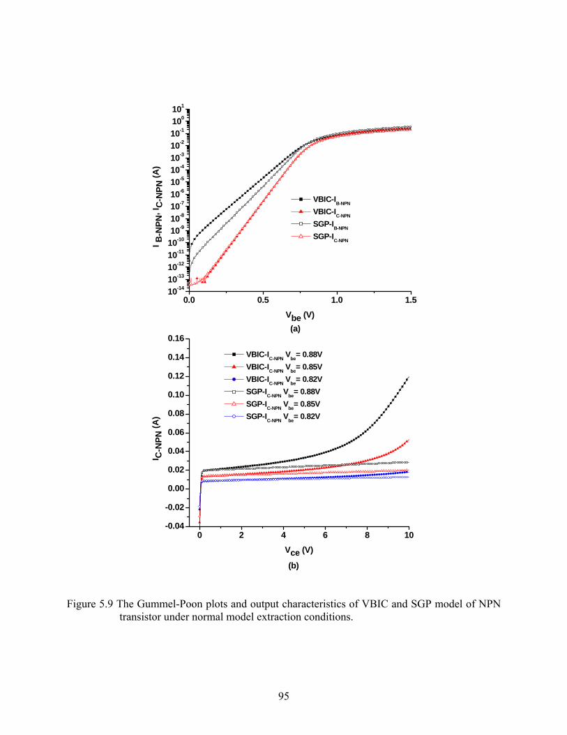
95
0.0 0.5 1.0 1.510-1410-1310-1210-1110-1010-910-810-710-610-510-410-310-210-1100101
0 2 4 6 8 10-0.04
-0.02
0.00
0.02
0.04
0.06
0.08
0.10
0.12
0.14
0.16
I B-N
PN, I
C-N
PN (A
)
Vbe (V)
VBIC-IB-NPN
VBIC-IC-NPN
SGP-IB-NPN
SGP-IC-NPN
(b)
(a)
I C-N
PN (A
)
Vce (V)
VBIC-IC-NPN Vbe= 0.88V VBIC-IC-NPN Vbe= 0.85V VBIC-IC-NPN Vbe= 0.82V SGP-IC-NPN Vbe= 0.88V SGP-IC-NPN Vbe= 0.85V SGP-IC-NPN Vbe= 0.82V
Figure 5.9 The Gummel-Poon plots and output characteristics of VBIC and SGP model of NPN transistor under normal model extraction conditions.
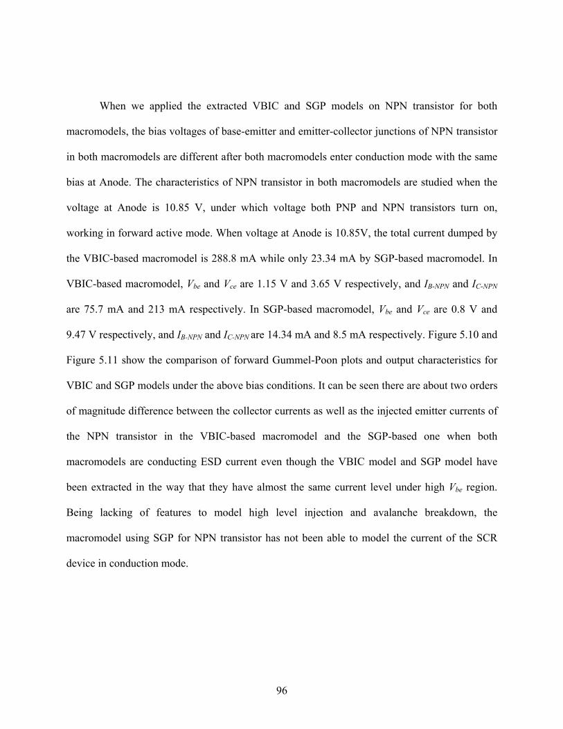
96
When we applied the extracted VBIC and SGP models on NPN transistor for both
macromodels, the bias voltages of base-emitter and emitter-collector junctions of NPN transistor
in both macromodels are different after both macromodels enter conduction mode with the same
bias at Anode. The characteristics of NPN transistor in both macromodels are studied when the
voltage at Anode is 10.85 V, under which voltage both PNP and NPN transistors turn on,
working in forward active mode. When voltage at Anode is 10.85V, the total current dumped by
the VBIC-based macromodel is 288.8 mA while only 23.34 mA by SGP-based macromodel. In
VBIC-based macromodel, Vbe and Vce are 1.15 V and 3.65 V respectively, and IB-NPN and IC-NPN
are 75.7 mA and 213 mA respectively. In SGP-based macromodel, Vbe and Vce are 0.8 V and
9.47 V respectively, and IB-NPN and IC-NPN are 14.34 mA and 8.5 mA respectively. Figure 5.10 and
Figure 5.11 show the comparison of forward Gummel-Poon plots and output characteristics for
VBIC and SGP models under the above bias conditions. It can be seen there are about two orders
of magnitude difference between the collector currents as well as the injected emitter currents of
the NPN transistor in the VBIC-based macromodel and the SGP-based one when both
macromodels are conducting ESD current even though the VBIC model and SGP model have
been extracted in the way that they have almost the same current level under high Vbe region.
Being lacking of features to model high level injection and avalanche breakdown, the
macromodel using SGP for NPN transistor has not been able to model the current of the SCR
device in conduction mode.
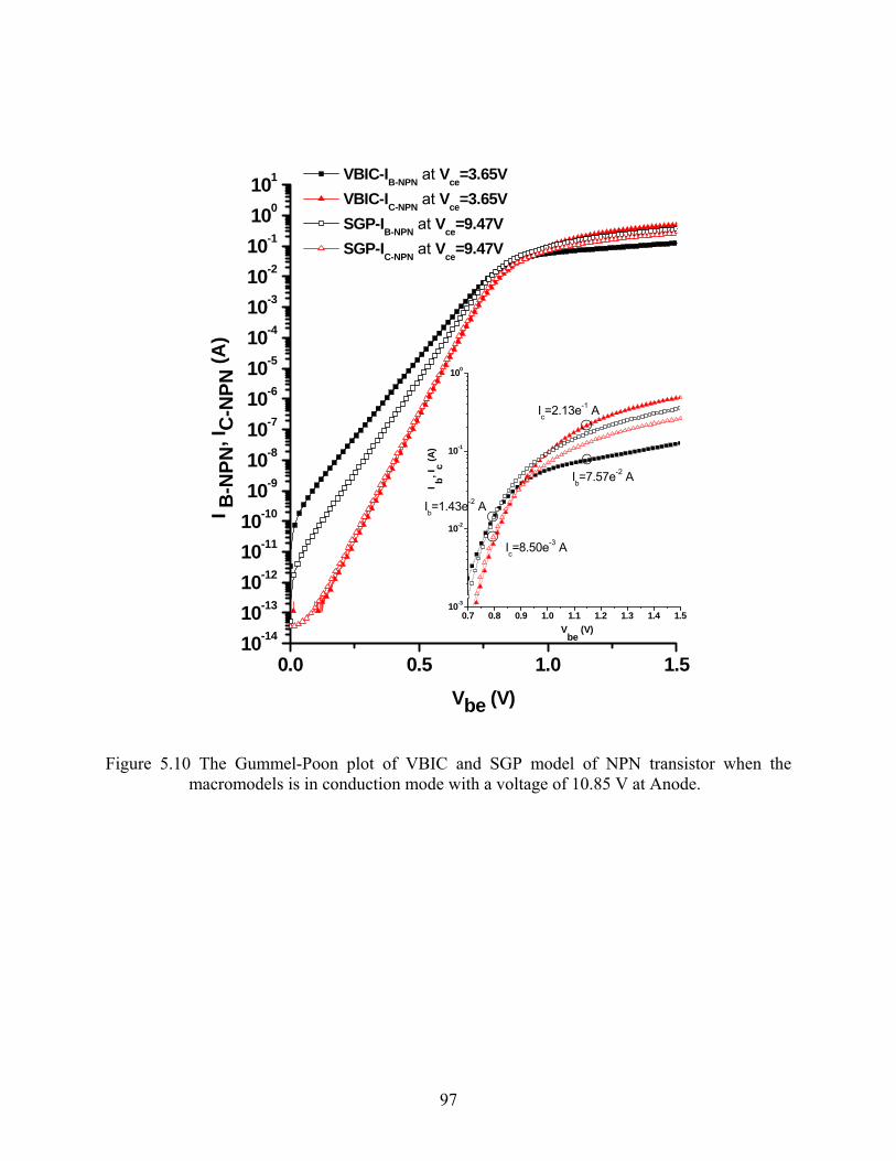
97
0.0 0.5 1.0 1.510-14
10-13
10-12
10-1110-10
10-9
10-8
10-7
10-6
10-5
10-4
10-310-2
10-1
100
101
0.7 0.8 0.9 1.0 1.1 1.2 1.3 1.4 1.510-3
10-2
10-1
100
I b, Ic (A
)
Vbe
(V)
Ic=8.50e-3 A
Ib=1.43e-2 A
Ic=2.13e-1 A
Ib=7.57e-2 A
I B-N
PN, I
C-N
PN (A
)
Vbe (V)
VBIC-IB-NPN at Vce=3.65V VBIC-IC-NPN at Vce=3.65V SGP-IB-NPN at Vce=9.47V SGP-IC-NPN at Vce=9.47V
Figure 5.10 The Gummel-Poon plot of VBIC and SGP model of NPN transistor when the macromodels is in conduction mode with a voltage of 10.85 V at Anode.
98
0 2 4 6 8 10-0.050.000.050.100.150.200.250.300.350.400.450.500.550.60
Ic=2.13e-1 A
Ic=8.50e-3 A
I C-N
PN (A
)
Vce (V)
VBIC-IC-NPN at Vbe= 1.15V SGP-IC-NPN at Vbe= 0.80V
Figure 5.11 The output characteristics of VBIC and SGP model of NPN transistor when the macromodels is in conduction mode with a voltage of 10.85 V at Anode.
5.3.3. Negative Operation Region
The negative characteristic of the HH-LVTSCR is like a forward-biased diode, as the
TLP measurements in Figure 5.6. With the terminal connection as in Figure 5.3 and Figure 5.4,
when under the reverse bias, the P-Well/N-Well and P-Substrate/N-Well junction diodes are
forward biased and diode-mode conduction results. The P-Substrate/N-Well junction has been
modeled by Dsub. The current path going through Dsub under reverse bias is denoted as P1 in
99
Figure 5.3(a) and Figure 5.4(a). The P-Well/N-Well junction is the base-collector junction of the
PNP transistor as well as the NPN transistor. It has been modeled within the respective SGP-PNP
model and VBIC-NPN model in the VBIC-based macromodel, and SGP-PNP model and SGP-
NPN model in the SGP-based macromodel. The current path going through P-Well/N-Well
junction diode under reverse bias is denoted as P2 in Figure 5.3(a) and Figure 5.4(a). There is
one more current path going through the base-collector junction of the Parasitic-PNP transistor
built in VBIC, denoted as P3 (see Figure 5.3(a)).
For the SGP-based macromodel, there are only current path P1 and P2, the simulation
results can not fit the TLP measurement results since the coupled PNP and NPN transistor
models can not function correctly as a forward biased diode under reverse bias. With the built-in
parasitic PNP transistor, we have additional current path, P3, parallel with P1 and P2 to conduct
more reverse current.
5.4. Chapter Summary
In this chapter, we presented two SCR macromodels by using VBIC model and SGP
model respectively to describe the NPN bipolar transistor in the macromodel. The simulation
results of the VBIC-based macromodel shows excellent match with measurements while those of
the SGP-based macromodel do not. Comparing with SGP-based macromodel, the VBIC-based
macromodel has one more current source, avalanche breakdown current, to contribute to the total
generation current, which makes the macromodel predict the trigger and holding voltages
correctly. In additional to the avalanche current model, the VBIC model models the quasi-
saturation behavior to describe high level injection, which makes the VBIC-based macromodel is

100
accurate in conduction mode. Moreover, the parasitic PNP built in VBIC model supplies
additional current path in negative operation, which make the simulation results of the VBIC-
based macromodel fit the TLP measurements well in reverse direction. Being lake of the above
advanced features, the SCR macromodel by using SGP for NPN transistor has not been a
successful model.
101
CHAPTER 6. CONCLUSIONS
ESD failure is a stringent reliability problem to semiconductor industry. Up to one third
of all ICs failure might be attributed to ESD. The dissertation firstly talks about how ESD events
happen and how they related to failures of integrated circuits, which is followed by models of
ESD events and characterization of ESD performance in ICs. Then the dissertation leads the
topic to how to reduce ICs failures due to ESD. One of the most important ways is to incorporate
on-chip ESD protection inside ICs. The main contributions of this dissertation are having
designed and integrated the novel ESD protection devices for low- and high-voltage applications
and having developed and implemented the accurate compact model of the ESD protection
device in SPICE-like circuit simulator to optimize ESD design and predict ESD performance at
pre-silicon stages.
A novel SCR device, called uSCR, has been presented in this dissertation for ESD
protection applications of low-voltage ICs. This is the first time an SCR can possess a trigger
voltage as low as 7 V without using any external triggering circuitry and a holding voltage as
high as 6 V without sacrificing the ESD robustness, while at the same time consuming an area of
only 2400 μm2. The ESD protection robustness of the uSCR in both positive and negative
operations exceeds 60 mA/μm, which enables ESD protection levels of +/- 8 kV HBM and +/- 2
kV CDM for a low voltage ICs.
For high voltage technologies, the first important issue the snapback-type ESD protection
device has to face is how to avoid latch-up. Increase the holding current is an efficient solution.
102
The holding current of SCR device is dependent on the avalanche multiplication factor, M, and
the current gains of the PNP and NPN transistors in SCR device. A novel high holding current
SCR (HHC-SCR) has been developed in this dissertation for high voltage applications and test
devices have been fabricated on the BiCMOS 0.6 μm process. The TLP measurement results
have shown that by reaching a maximal M(IC-PNP+IC-NPN), the HHC-SCR device has realized a
holding current as high as 24 mA/μm to effectively avoid latch-up and a high failure current (48
mA/μm) for ESD robustness. Additionally, without involving any external circuitry or extra
devices, the HHC-SCR device releases reliability weakness issues and accomplishes the
minimum area consumption.
In additional to the on-chip ESD protection design, this dissertation has presented a
comprehensive compact model of SCR for the simulation of integrated circuits subjected to a
pervasive CDM ESD event. The work illustrated the useful and effective macromodeling
approach of integrating the various industry standard models to describe the individual devices
imbedded in the SCR. In addition, the modeling of the avalanche current sources, substrate
parastics, and capacitances were discussed. The issue of parameter extraction was addressed as
well. This modeling approach offers simplicity, wide availability and compatibility with most
commercial simulators by taking advantage of using the advanced BJT model, VBIC. The
presented model is implemented into the industry standard Cadence SPICE to study the CMOS
circuit response to CDM stress. Application to 0.35-μm technology SPDT analog switch I/O
circuits demonstrates effectiveness in analyzing CDM response and quantitatively predicting
withstand levels.
103
In the end, this dissertation compared two SCR macromodels by using VBIC model and
SGP model respectively to describe the NPN bipolar transistor in the SCR macromodel. The
simulation results of the VBIC-based macromodel shows excellent match with measurements
while those of the SGP-based macromodel do not. The avalanche current model, the quasi-
saturation model and the parasitic substrate transistor model built in VBIC model give the VBIC-
based macromodel capability to predict the trigger and holding voltages correctly, to perform in
conduction model accurately and to the dump enough current in reverse operation region to fit
the TLP measurement results. Being lake of the above advanced features, the SCR macromodel
by using SGP for NPN transistor has not been able to be a successful model.
104
LIST OF REFERENCES
[1] A. Wang, On-Chip ESD Protection for Integrated Circuits, Boston: Kluwer Academic
Publishers, 2002.
[2] T. J. Green and W. K. Denson, “A review of EOS/ESD field failures in military
equipment,” in Proceedings of EOS/ESD Symposium, 1988, pp. 7-14.
[3] W. D. Greason, “Electrostatic discharge: A charge driven phenomenon,” in Proc.
EOS/ESD Symposium, vol. EOS-13, Sept. 1991, pp. 1-9.
[4] International Technology Roadmap for Semiconductors, http://www.itrs.net, 2007.
[5] SEMATECH International, “Critical reliability challenges for the international technology
roadmap for semiconductor (ITRS),” SEMATECH DOC ID # 03024377A-TR, 2003.
[6] A. Amerasekera and C. Duvvury, “The impact of technology scaling on ESD robustness
and protection circuit design,” IEEE Transaction Component, Packaging and
Manufacturing Technology, Part A, vol. 21, no. 4, pp. 314-320, June 1995.
[7] S. H. Voldman, L. Lanzerotti, W. Morris, and L. Rubin, “A review of electrostatic
discharge (ESD) in advanced semiconductor technology,” Journal of Microelectronics
Reliability, vol. 44, no. 1, pp. 33-46, Jan 2004.
[8] S. H. Voldman, “A review of latchup and electrostatic discharge (ESD) in BiCMOS RF
silicon germanium technologies: Part I-ESD”, Journal of Microelectronics Reliability, vol.
45, no. 2, pp. 323-340, Feb 2005.

105
[9] S. H. Voldman, “A review of CMOS latchup and electrostatic discharge (ESD) in bipolar
complimentary MOSFET (BiCMOS) Silicon Germanium technologies: Part II–Latchup,”
Journal of Microelectronics Reliability, vol. 45, no. 3-4, pp. 437-455, Apr 2005.
[10] R. Glenn Wagner, J. M. Soden, and C. F. Hawkins, “Extent and Cost of EOS/ESD Damage
in an IC Manufacturing Process,” in Proceedings of EOS/ESD Symposium, 1993, pp. 49-55.
[11] T. J. Green and W. K. Denson, “Review of EOS/ESD Field Failures in Military
Equipment,” in Proceedings of EOS/ESD Symposium, 1988, pp. 7-14.
[12] A. Amerasekera and C. Duvvury, ESD in Silicon Integrated Circuits, 2nd ed., England:
John Wiley, 2002.
[13] J. E. Vinson, J. C. Bernier, G. D. Croft and J. J. Liou, ESD Design and Analysis Handbook,
Boston: Kluwer Academic Publishers, 2003.
[14] S. H. Voldman, ESD Circuits and Devices. England: Wiley, 2006.
[15] D. G. Pierce and D. L. Durgin, “An overview of electrical overstress effects on
semiconductor devices,” in Proceedings of EOS/ESD Symposium, 1981, pp.120-131.
[16] D. G. Pierce, “Electrostatic Discharge (ESD) Failure Mechanisms”, EOS/ESD Tutorial
Notes, 1995, pp. C-1 to C-32.
[17] S. Dabral and T. J. Maloney, Basic ESD and I/O Design, John Wiley & Sons, Inc., 1998.
[18] T. S. Speakman, “A model for the failure of bipolar silicon integrated circuits subjected to
electrostatic discharge,” in Proceedings of International Reliability Physics Symposium,
1974, pp.60-67.
106
[19] M. J. Middendorf and T. Hausken, “Observed physical effects and failure analysis of
EOS/ESD in MOS devices,” in Proceedings of International Symposium for Testing and
Failure Analysis, 1984, pp. 205-213.
[20] JEDEC Solid State Technology Association, “Electrostatic Discharge (ESD) Sensitivity
Testing Human Body Model (HBM),” JESD22-A114E, Jan 2007, [Online] available:
http://www.jedec.org.
[21] Electrostatic Discharge Association, “Electrostatic Discharge Sensitivity Testing – Human
Body Model (HBM) Component Level,” ANSI/ESD STM5.1-2007, Nov 2007, [Online]
available: http://www.esda.org.
[22] Electronic Industries Association, “Electrostatic Discharge (ESD) Sensitivity Testing
Machine Model (MM),” EIA/JESD22-A115-A, Oct 1997, [Online] available:
http://www.jedec.org.
[23] Electrostatic Discharge Association, “Electrostatic Discharge Sensitivity Testing –
Machine Model (MM) Component Level,” ANSI/ESD STM5.2-1999, [Online] available:
http://www.esda.org.
[24] JEDEC Solid State Technology Association, “Field-Induced Charged-Device Model Test
Method for Electrostatic-Discharge-Withstand Thresholds of Microelectronic
Components,” JESD22-C101C, Dec 2004, [Online] available: http://www.jedec.org.
[25] Electrostatic Discharge Association, “Electrostatic Discharge Sensitivity Testing –
Charged Device Model (CDM) Component Level,” ANSI/ESD STM5.3.1-1999, [Online]
available: http://www.esda.org.
107
[26] S. Ramaswamy, E. Li, E. Rosenbaum, and S. M. Kang, “Circuit-level simulation of CDM
and EOS in submicron MOS devices,” in Proceedings of EOS/ESD Symposium, 1996, pp.
316.
[27] J. Lee, K. W. Kim, Y. Huh, P. Bendix, and S.M. Kang, “Chip-level charge-device
modeling and simulation in CMOS integrated circuits,” IEEE Trans. on Computer-Aided
Design of Integrated Circuits and Systems, vol. 22, p.67, 2003.
[28] International Electrotechnical Commission, “Electromagnetic Compatibility (EMC) – Part
4-2: Testing and Measurement Techniques – Electrostatic Discharge Immunity Test,” IEC
61000-4-2, Apr 2001, [Online] available: http://www.iec.ch.
[29] T. Maloney and N. Khurana, “Transmission Line Pulsing Technique for Circuit Modeling
of ESD Phenomena,” in Proceedings of EOS/ESD Symposium, 1985, pp. 49-54.
[30] J. Barth, K. Verhaege, L. Henry and J. Richner, “TLP Calibration, Correlation, Standards,
and New Techniques,” in Proceedings of EOS/ESD Symposium, 2000, pp. 85-96.
[31] JEDEC Solid State Technology Association, “Electrostatic Discharge Sensitivity Testing –
Transmission Line Pulse (TLP) – Component Level,” ANSI/ESD STM5.5.1-2008, [Online]
available: http://www.esda.org.
[32] M. Lee, C. Liu, C.-C. Lin, J.-T. Chou, H. Tang, Y. Chang, and K. Fu, “Comparison and
correlation of ESD HBM (Human Body Model) obtained between TLPG, wafer-level, and
package-level tests,” in Proceedings of EOS/ESD Symposium, 2000, pp. 105.
[33] J. E. Vinson and J. J. Liou, “Electrostatic discharge in semiconductor devices: protection
techniques,” in Proceedings of the IEEE, vol. 88, no. 12, pp.1878-1902, 2000.
108
[34] R. N. Rountree, “ESD protection for submicron CMOS circuits: Issues and Solutions,” in
IEDM Technology Digest, 1988, pp. 580-583.
[35] J. E. Vinson and J. J. Liou, “Electrostatic discharge in semiconductor devices: an overvie,”
in Proceedings of the IEEE, vol. 86, no. 2, pp. 399-420, Feb 1998.
[36] J. E. Vinson and J. J. Liou, “Electrostatic discharge in semiconductor devices: overview of
circuit protection techniques,” in Proceedings of the IEEE Hong Kong Electron Device
Meeting, 2000, pp. 5-8.
[37] L. A. Avery, “A review of electrostatic discharge mechanisms and on-chip protection
techniques to ensure device reliability,” J. Electrostatics, vol. 24, no. 2, pp. 111-113, 1990.
[38] A. Wang and C-H. Tsay, “On a dual-polarity on-chip electrostatic discharge protection
structure,” IEEE Trans. Electron Devices, vol. 48, pp. 978, 2001.
[39] G. Croft and J. Bernier, “ESD protection techniques for high frequency integrated
circuits,” Journal of Microelectronics Reliability, vol. 38, pp. 1681, 1998.
[40] C. Duvvury and C. Diaz, “Dynamic gate coupling of NMOS for efficient output ESD
protection,” in Proceedings of International Reliability Physics Symposium, 1992, pp. 141-
150.
[41] E. Worley, R. Gupta, B. Jones, R. Kjar, C. Nguyen, and M. Tennyson, “Sub-micron Chip
ESD Protection Schemes Which Avoid Avalanching Junctions,” in Proceedings of
EOS/ESD Symposium, 1995, pp 13-20.
[42] R. Merril, and E. Issaq, “ESD design methology,” in Proceedings of EOS/ESD Symposium,
1993, pp. 233-238.

109
[43] T. Maloney and S. Dabral, “Novel Clamp Circuits fro IC Power Supply Protection,” in
Proceedings of EOS/ESD Symposium, 1995, pp. 151-161.
[44] W. Anderson, J. Montanaro and N. Howorth, “Cross-Referenced ESD Protection for
Power Supplies,” in Proceedings of EOS/ESD Symposium, 1998, pp. 86-95.
[45] C. A. Torres, J. W. Miller, M. Stockinger, M. Akers, M. G. Khazhinsky, and J. C. Weldon,
“Modular, Portable, and Easily Simulated ESD Protection Networks for Advanced CMOS
Technologies,” in Proceedings of EOS/ESD Symposium, 2001, pp. 82-95.
[46] J. C. Smith and G. Boseli, “A MOSFET Power Supply Clamp with Feedback Enhanced
Triggering for ESD Protection in Advanced CMOS Technologies,” in Proceedings of
EOS/ESD Symposium, 2003.
[47] M. Stockinger, J. W. Miller, M. G. Khazhinsky, C. A. Torres, J. C. Weldon, B. D. Preble,
M. J. Bayer, M. Akers, and V. G. Kamat, “Advanced rail clamp networks for ESD
protection,” Microelectronics Reliability, vol. 45, no. 2, pp. 211-222, Feb 2005.
[48] M. Stockinger, J. W. Miller, M. G. Khazhinsky, C. A. Torres, J. C. Weldon, B. D. Preble,
M. J. Bayer, M. Akers, V. G. Kamat “Boosted and Distributed Rail Clamp Networks for
ESD Protection in Advanced CMOS Technologies”, Proc. EOS/ESD Symposium, 2003, pp
17-26.
[49] S. Voldman, Latchup, Hoboken, NJ: Wiley, 2007.
[50] S. English, E. Nestler, and A. Olney, “General purpose EOS/ESD protection circuit for
bipolar-CMOS and CMOS integrated circuits,” US Patent 5,917,689, 1999.
110
[51] J. Chen, X. Zhang, A. Amerasekera, and T. Vrotsos, “Design and layout of a high ESD
performance npn structure for submicron BiCMOS/bipolar circuits,” in Proceedings of
IRPS, 1996, pp. 227-232.
[52] A. Amerasekera, S. Ramaswamy, M.-C. Chang, and C. Duvvury, “Modeling MOS
snapback and parasitic bipolar action for circuit-level ESD and high current simulations,”
in Proceedings of IEEE International Reliability Physics Symposium, 1996, pp. 318.
[53] J. Z. Chen, A. Amerasekera and C. Duvvury, “Design methodology and optimization of
gate-driven NMOS ESD protection circuits in submicron CMOS processes,” IEEE
Transaction on Electron Device, vol. 45, no. 12, pp. 2448-2456, Dec 1998.
[54] A. Amerasekera, C. Duvvury, V. Reddy and M. Rodder, “Substrate triggering and silicide
effects on ESD performance and protection circuit design in deep submicron CMOS
process,” in IEDM Technology Digest, 1995, pp. 547-555.
[55] C. Duvvury, S. Ramaswamy, A. Amerasekera, R. Cline, B. Andresen and V. Gupta,
“Substrate Pump NMOS for ESD Protection Applications,” in Proceedings of. EOS/ESD
Symposium, 2000, pp. 7-14.
[56] K. Mistry, D. Krakauer, and B. Doyle, “Impact of snapback-induced hole injection on gate
oxide reliability of N-MOSFETs,” IEEE Electron Device Letters, vol. 11, pp. 460, 1990.
[57] M.-D. Ker, and K.-C. Hsu, “Overview of on-chip electrostatic discharge protection design
with SCR-based devices in CMOS integrated circuits,” IEEE Trans. on Devices and
Materials Reliability, vol. 5, pp. 235, June 2005.

111
[58] M. Corsi, R. Nimmo, and F. Fattori, “ESD protection of BiCMOS integrated circuits which
need to operate in the harsh environments of automotive or industrial,” in Proceedings of
EOS/ESD Symposium, 1993, pp. 209.
[59] J. A. Salcedo, Design and Characterization of Novel Devices for New Generation of
Electronstatic Discharge (ESD) Protection Structures, Ph.D. Thesis, University of Central
Florida, 2006.
[60] S. H. Voldman, ESD Physics and Devices, England: Wiley, 2004.
[61] C. Russ, M. P. J. Mergens, J. Armer, P. Jozwiak, G. Kolluri, L. Avery, and K. Verhaege,
“GGSCR: GGNMOS triggered silicon controlled rectifiers for ESD protection in deep
submicron CMOS processes,” in Proceedings of EOS/ESD Symposium, 2001, pp. 22-31.
[62] A. Chatterjee and T. Polgreen, “A low Voltage Triggering SCR for On-Chip ESD
Protection at Output an Input Pads,” IEEE Electron Device Lett., vol. 12, no. 1, pp. 21-22,
Jan. 1991.
[63] J. Salcedo and J. J. Liou, “A novel dual-polarity device with symmetrical/asymmetrical S-
type I-V characteristics for ESD protection design,” IEEE Electron Device Lett., vol. 27,
no. 1, pp. 65-67, Jan. 2006.
[64] L. R. Avery, “Using SCRs as transient protection structures in integrated circuits,” in
Proceedings of EOS/ESD Symposium, 1983, pp. 17.
[65] M.-D. Ker, H.-H. Chang, and C.-Y. Wu, “A gate-coupled PTLSCR/NTLSCR ESD
protection circuit for deep-submicron low-voltage CMOS ICs,” IEEE J. Solid-State
Circuits, vol. 32, no. 1, pp. 38-51, Jan. 1997.
112
[66] M.-D. Ker and K.-C. Hsu, “SCR devices with double-triggered technique for on-chip ESD
protection in sub-quarter-micron silicided CMOS processes,” IEEE Trans. Device Mater.
Reliab., vol. 3, no. 3, pp. 58-68, Sep. 2003.
[67] F. Azaïs, B. Caillard, S. Dournelle, P. Salomé and P. Nouet, “A new multi-finger SCR-
based structure for efficient on-chip ESD protection,” Microelectronics and Reliability, vol.
45, no. 2, pp. 233-243, Feb 2005.
[68] M.-D. Ker, “Lateral SCR devices with low-voltage high-current triggering characteristics
for output ESD protection in submicron CMOS technology,” IEEE Trans. Electron
Devices, vol. 45, no. 4, pp. 849-860, Apr. 1998.
[69] M. P. J. Mergens, C. C. Russ, K. G.Verhage, J. Armer, P. C. Jozwiak, and R. Mohn, “High
holding current SCRs (HHI-SCR) for ESD protection and latch-up immune IC operation,”
in Proc. EOS/ESD Symp., 2002, pp. 10-17.
[70] C.-H. Lai, M.-H. Liu, S. Su, T.-C. Lu, and S. Pan, “A novel gate-coupled SCR ESD
protection structure with high latchup immunity for highspeed I/O pad,” IEEE Electron
Device Lett., vol. 25, no. 5, pp. 328-330, May 2004.
[71] Ming-Dou Ker; Zi-Ping Chen, “SCR device with dynamic holding voltage for on-chip
ESD protection in a 0.25-/spl mu/m fully salicided CMOS process,” IEEE Transactions on
Electron Devices, vol. 51, no. 10, Oct 2004, pp.1731-1734.
[72] L. Lou and J. J. Liou, “An Unassisted, Low Trigger-, and High Holding-Voltage SCR
(uSCR) for On-Chip ESD-Protection Applications,” IEEE Electron Device Lett., vol. 28,
no. 12, pp. 1120-1122, Dec 2007.
113
[73] L. Lou and J. J. Liou, “A Novel and Robust Un-Assisted, Low-Trigger and High-Holding
Voltage SCR (uSCR) for Area-Efficient On-Chip ESD Protection,” in Proceedings of
IEEE Conference on Electron Devices and Solide-State Circuits, 2007, pp. 605-607.
[74] L. Lou and J. J. Liou, “A novel low-trigger and high-holding voltage SCR without
externally- assisted circuitry for area-efficient on-chip ESD protection,” in Proceedings of
International Semiconductor Device Research Symposium, 2007, pp. 1-2.
[75] B. Streetman and S. Baneriee, Solid State Electron Devices, 6th, Prentic Hall, 2005.
[76] B. Keppens, M. P. J. Mergens, C. S. Trinh, C. C. Russ, B. Van Camp, and K. G. Verhaege,
“ESD protection solutions for high voltage technologies,” Microelectronics Reliability, vol.
46, no. 5, pp. 677-688, May 2006.
[77] R. M. Steinhoff, J. Huang, P. L. Hower, and J. S. Brodsky, “Current filament movement
and silicon melting in an ESD-robust DENMOS transistor,” in Proceedings of EOS/ESD
Symposium, 2003. pp. 98-106.
[78] M. P. J. Mergens, W. Wilkening, S. Mettler; H. Wolf, A. Stricker; W. Fichtner, “Analysis
of lateral DMOS devices under ESD stress conditions,” IEEE Transaction of Electron
Devices, vol. 47, no. 11, pp. 2128-2137, Nov 2000.
[79] M. P. J. Mergens, K. G. Verhaege, C. C. Russ, J. Armer, P. C. Jozwiak, G. Kolluri, and L.
R. Avery, “Multi-finger turn-on circuits and design techniques for enhanced ESD
performance and width scaling,” in Proceedings of EOS/ESD Symposium, 2001. pp. 1-11.
[80] V. A. Vashchenko, A. Concannon, M. ter Beek, and P. Hopper, “High holding voltage
cascoded LVTSCR structures for 5.5-V tolerant ESD protection clamps,” IEEE Trans.
Device Mater. Rel., vol. 4, no. 2, pp. 273-280, June 2004.
114
[81] V. A. Vashchenko, A. Concannon, M. ter Beek, and P. Hopper, “Comparison of ESD
protection capability of lateral BJT, SCR and bidirectional SCR for high-voltage BiCMOS
circuits,” in Proc. BCTM, 2002, pp. 181-184.
[82] O. Quittard, Z. Mrcarica, F. Blanc, G. Notermans, T. Smedes, and H. van Zwol, “ESD
protection for high-voltage CMOS technologies,” in Proc. EOS/ESD Symp., 2006, pp. 77-
86.
[83] Z. Liu, J. J. Liou, and J. Vinson, “Novel silicon-controlled rectifier (SCR) for high-voltage
electrostatic discharge (ESD) applications,” IEEE Trans. Electron Devices, vol. 29, no. 7,
pp. 753-755, July 2008.
[84] S. M. Sze, Physics of Semiconductor Devices, 2nd ed., New York: John Wiley & Sons,
1981.
[85] D. B. Estreich, The Physics and Modeling of Latch-up in CMOS Integrated Circuits, Ph.D.
Thesis, Stanford University, 1981.
[86] P. Bossard, R. Chemelli, and B. Unger, “ESD damage from triboelectrically charged IC
pins,” in Proc. 2nd EOS/ESD Symp., 1980, pp.17-22.
[87] P. A. Juliano and E. Rosenbaum, “A novel SCR macromodel for ESD circuit simulation,”
in International Electron Devices Meeting, 2001, pp.14.3.1-14.3.4.
[88] J. Di Sarro and E. Rosenbaum, “A scalable SCR compact model for ESD circuit
simulation,” in International Reliability Physics Symposium, 2008, pp. 254-261.
[89] J. Rodriguez, M. C. Smayling, and W. L. Wilson, “ESD circuit synthesis and analysis
using TCAD and SPICE,” in International Electron Devices Meeting, 1998, pp. 97-100.
115
[90] F. Azaïs, B. Caillard, S. Dournelle, P. Salomé, and P. Nouet, “A new multi-finger SCR-
based structure for efficient on-chip ESD protection,” Microelectronics Reliability, vol. 45,
no. 2, pp. 233-243, Feb. 2005.
[91] Yuanzhong (Paul) Zhou, Jean-Jacques Hajjar, and Kenneth Lisiak, “Compact modeling of
on-chip ESD protection using standard MOS and BJT models,” in 8th International
Conference on Solid-State and Integrated Circuit Technology, 2006, pp. 1202-1205.
[92] Yuanzhong (Paul) Zhou, Jean-Jacques Hajjar, and Kenneth Lisiak, “Modeling snapback of
LVTSCR devices for ESD circuit simulation using advanced BJT and MOS models,” in
Proc. EOS/ESD Symp., 2007.
[93] J. A. Salcedo, J. J. Liou, and J. C. Bernier, “Novel and robust silicon-controlled rectifier
(SCR) based devices for on-chip ESD protection,” IEEE Electron Device Lett., vol. 25, no.
9, pp. 658-660, Sept. 2004.
[94] Lifang Lou and Juin J. Liou, “A Comprehensive SCR Compact Model for CDM ESD
Simulation,” in IEEE International Reliability Physics Symposium, 2008, pp. 635-636.
[95] C. Duvvury, A. Amerasekera, “Advanced CMOS protection device trigger mechanisms
during CDM,” IEEE Trans. Compon., Packag., Manuf. Technol. A, vol. 19, no. 3, pp. 169-
177, July 1996.
[96] S. M. Sze, Physics of Semiconductor Devices, 2nd ed., New York: John Wiley & Sons,
1981.
[97] BSIM3v3.3.0 Manual, Univ. California, Berkely, 2005.
[98] W. Liu, MOSFET Models for SPICE Simulation including BSIM3v3 and BSIM4, New
York: John Wiley & Sons, 2001.

116
[99] C. McAndrew, et al., “VBIC95, The Vertical Bipolar Inter-Company Model,” IEEE J.
Solid- State Circuits, vol.31, no.10, pp. 1476-1482, 1996.
[100] C. McAndrew, T. Bettinger, L. Lemaitre, and M. Tutt, "BJT Modeling with VBIC, Basics
and V1.3 Updates,” in Workshop of Compact Model, 2003, pp. 278-281.
[101] Agilent Technologies, “User’s Guide,” IC-CAP Documentation 2008, [Online] available:
http://cp.literature.agilent.com/litweb/pdf/iccap2008/iccap2008.html.
[102] “Slides on VBIC,” [Online] available: http://www.designers-
guide.org/VBIC/references.html.
[103] X. Cao, J. McMacken, K. Stiles, P. Layman, J. J. Liou, A. Sun and S. Moinian, “Parameter
Extraction and Optimization for New Industry Standard VBIC Model,” in Proceedings of
International Conference on Advanced Semiconductor Devices and Microsystems, 1998,
pp. 107-115.
[104] S. G. Beebe, “Simulation of complete CMOS I/O circuit response to CDM stress,” in Proc.
EOS/ESD Symp., 1998, pp. 259-270.
[105] H. Gummel and H. Poon, “A compact bipolar transistor model,” in Digest of Technical
Papers in IEEE ISSCC, 1970, pp. 78-79.
[106] Cadence Design System “Spectre Circuit Simulator Device Models and Circuit
Components,” Cadence User Documents, 2008.