DESIGN AND IMPLEMENTATION OF GATE DIFFUSION INPUT …
152
DESIGN AND IMPLEMENTATION OF GATE DIFFUSION INPUT BASED VEDIC MULTIPLIER A THESIS by SHOBA M submitted to Pondicherry University in fulfilment for the award of the degree of DOCTOR OF PHILOSOPHY in ELECTRONICS AND COMMUNICATION ENGINEERING DEPARTMENT OF ELECTRONICS ENGINEERING SCHOOL OF ENGINEERING AND TECHNOLOGY PONDICHERRY UNIVERSITY PONDICHERRY - 605 014, INDIA AUGUST 2016
Transcript of DESIGN AND IMPLEMENTATION OF GATE DIFFUSION INPUT …

DESIGN AND IMPLEMENTATION OF GATE
DIFFUSION INPUT BASED VEDIC
MULTIPLIER
A THESIS
by
SHOBA M
submitted to Pondicherry University in fulfilment for the award of the
degree of
DOCTOR OF PHILOSOPHY
in
ELECTRONICS AND COMMUNICATION ENGINEERING
DEPARTMENT OF ELECTRONICS ENGINEERING
SCHOOL OF ENGINEERING AND TECHNOLOGY
PONDICHERRY UNIVERSITY
PONDICHERRY - 605 014, INDIA
AUGUST 2016

ii
DEPARTMENT OF ELECTRONICS ENGINEERING SCHOOL OF ENGINEERING AND TECHNOLOGY
PONDICHERRY UNIVERSITY PONDICHERRY- 605 014, INDIA
DECLARATION
I certify to the best of my knowledge that the work reported in this
thesis has not been previously submitted for a degree nor it is based on any
other dissertation which a degree or award was conferred on an earlier
occasion for any other candidate.
I also certify that the thesis has been written by me and any help that
I have received in my research work has been acknowledged. In addition, I
certify that all information sources and literature used are indicated in the
thesis.
Place: Pondicherry (M.SHOBA)
Date :

iii
DEPARTMENT OF ELECTRONICS ENGINEERING SCHOOL OF ENGINEERING AND TECHNOLOGY
PONDICHERRY UNIVERSITY PONDICHERRY- 605 014, INDIA
BONAFIDE CERTIFICATE
It is certified that this thesis titled “DESIGN AND
IMPLEMENTATION OF GATE DIFFUSION INPUT BASED VEDIC
MULTIPLIER” is the bonafide work of Mrs. M. SHOBA who carried out
the research under my supervision. Further certified that to the best of my
knowledge the work reported herein does not form part of any other thesis or
dissertation on the basis of which a degree or award was conferred on an
earlier occasion for this or any other candidate.
Dr. R. NAKKEERAN
(Research Supervisor)
Associate Professor and Head
Dept. of Electronics Engineering
School of Engg. and Technology
Place: Pondicherry Pondicherry University
Date : Pondicherry- 605 014

iv
ABSTRACT
The objective of this research is to design a multiplier which poses
better performance in terms of area, delay and power consumption. The
performance of the multiplier can be greatly influenced by the chosen logic
style. In this work, Gate Diffusion Input (GDI) logic is considered. It is a low
power design technique which can implement any function with low transistor
count. However, this logic has the drawback of producing reduced voltage
swing at their outputs, i.e. the output high (or low) voltage deviated from the
VDD (or GND) by threshold voltage Vt. The existing techniques for obtaining
full swing suffer from having more transistor count or high power
consumption. To overcome this issue, a method is proposed by placing
additional transistor PMOS or NMOS at the output, based on the requirements
of VDD or GND output voltage, respectively. Based on this approach, a set of
full swing GDI gates namely, AND, OR, XOR and XNOR are proposed.
Further, three full adders are designed with the help of these full swing gates.
In addition, a new architecture for 4-2 compressor design is proposed in this
thesis, which is based on simplification of its Boolean output expression. The
partial sharing of architecture between sum and carry output minimizes the
hardware components which in turn reduces the area. Not only that, the
removal of redundant hardware minimizes the spurious switching activities
thus saving power. Also, the performance of the parallel adders namely,
Ripple Carry Adder (RCA), Carry Select Adder (CslA) and Carry Look
Ahead (CLA) adder are improved using proposed gates and adder in GDI
logic.
Further, the implementation of the multiplier based on Vedic
mathematics is discussed. Vedic mathematics is an ancient Indian
mathematics, which has been derived from Vedic sutras. Urdhva
Triyagbhyam (UT) is one of the Vedic sutras, which literally means

v
vertically and crosswise to perform the multiplication operation. During a
multiplication process The existing UT multiplier designs exhibit shorter
delay at the expense of larger area. This issue can be mitigated by dividing
the multiplication into two stages and each stage the computation shall be
performed in parallel. Moreover, the deployment of compressor based partial
product accumulation decreases the delay. This proposed multiplier is
implemented using GDI logic. Finally, a new architecture for the hierarchy
multiplier design is proposed by employing carry select adder and Binary to
Excess 1 Converter (BEC). The use of BEC eliminates the n/4 number of
adders, presented in the conventional hierarchy multiplier where n denotes the
multiplier input bit, thereby improving its speed of operation. The building
blocks of hierarchy multiplier are designed using GDI logic.
The power consumption and delay of all the proposed modules and the
related existing designs are analyzed through SPICE simulation at 45 nm
technology model and their area is calculated from the layout. Further, the
robustness of all the proposed modules with respect to process changes is
validated by Monte Carlo simulation.

vi
ACKNOWLEDGEMENT
The journey of my doctoral studies at Pondicherry University has not
been a painless mission and would never have been possible without the help
and support of several people to whom I want to express my earnest gratitude.
Primarily, I would like to express my profound and sincere gratitude to
my research supervisor, Dr. R. Nakkeeran, Associate Professor and Head,
Department of Electronics Engineering, School of Engineering and
Technology, Pondicherry University, Puducherry for his constant
encouragement, insightful discussions, inspiring words and invaluable
guidance during numerous technical discussions that have found their way
into this dissertation. His wide knowledge and logical way of thinking have
been of great value to overcome the obstacles in my research.
I would also like to thank my doctoral committee members
Dr. P. Sivaprakasam, Associate Professor, Department of Physics,
Pondicherry University, Puducherry and Dr. T. Shanmuganantham,
Assistant Professor, Department of Electronics Engineering, Pondicherry
University, Puducherry for their valuable remarks, recommendation and
suggestion at all stages of my research.
I am extremely grateful to Dr. S. Kanmani, Professor, Department of
Information Technology, Pondicherry Engineering College, Puducherry for
her constant motivation, guidance and moral support during my research
period.
I would like to thank my senior and co-research folks, Dr. J. William,
Dr. M. Thachayani, Mr. M. Ramasamy, Dr. K. Thirumalaivasan,
Dr. R. Ramya, Dr. S. Robinson, Mr. M. Rathinasabapathy,
Dr. A. Rajesh, Mr. G. Idayachandran and Mrs. S. Fouziya Sulthana, Mr.

vii
Enamul Haq Sheik, Finitha Jose and Mrs. Anitha Soman for their
motivation, help and moral support.
It is also my pleasure to express my grateful thanks to
Prof. R. Subramanian, former Dean, School of Engineering and Technology,
and Dr. P. Dhanavanthan, Dean, School of Engineering and Technology,
Pondicherry University, Puducherry facilitating me to pursue the research
work.
I would like to acknowledge the support from University Grants
Commission, Government of India under Junior Research Fellowship
scheme.
I greatly appreciate the support of the Department of Electronics
Engineering office staff members including Mr. N. Gokulan,
Mr. B. Santhanakrishnan, Mr. K. Kaliamoorthy and Mr. N. Soureche.
I am greatly indebted to my parents, sister, husband, in laws and my
baby for their endless love and unconditional support to pursue my interests,
which are vital for the completion of my Ph.D study. I received many help
from unknown hands. A very special thanks to all of them.
Finally, I thank the almighty God for the endless blessings to complete
this work successfully.
M. SHOBA

viii
This thesis is dedicated
to my beloved sister
Deepa Mohan

ix
TABLE OF CONTENTS
CHAPTER NO. TITLE PAGE NO.
ABSTRACT iv
ACKNOWLEDGEMENT vi
LIST OF FIGURES xiii
LIST OF TABLES xv
LIST OF SYMBOLS xvii
LIST OF ABBREVIATIONS xviii
1
INTRODUCTION
1.1 PREAMBLE
1
1.2 OBJECTIVES 2
1.3 LITERATURE SURVEY 3
1.3.1 Logic Styles 3
1.3.2 Full Adder 7
1.3.3 4-2 Compressor 9
1.3.4 Parallel Adders 11
1.3.5 Vedic Multiplier 13
1.3.6 Hierarchy Multiplier 18
1.4 ORGANIZATION OF THE THESIS 19
2
DESIGN OF FULL SWING GATES AND FULL
ADDER USING GDI LOGIC
2.1 INTRODUCTION
21
2.2 GDI LOGIC 22
2.2.1 Design of Gates using GDI Logic 24

x
CHAPTER NO. TITLE PAGE NO.
2.2.2 Full Swing AND, OR, XOR and XNOR
Gates 27
2.3 FULL ADDER DESIGNS 32
2.4 RESULTS AND DISCUSSION 35
2.4.1 Performance Analysis of AND, OR, XOR
and XNOR Gates 35
2.4.2 Performance Analysis of Full Adder 41
2.5 SUMMARY 47
3 AREA AND ENERGY EFFICIENT 4-2 COMPRESSOR
DESIGN USING GDI LOGIC
3.1 INTRODUCTION 49
3.2 RELATED WORKS OF 4-2 COMPRESSOR 50
3.3 METHODOLOGY 53
3.3.1 Proposed 4-2 Compressor 53
3.3.2 GDI Logic 55
3.4 RESULTS AND DISCUSSION 56
3.5 SUMMARY 60
4 PERFORMANCE IMPROVEMENT OF PARALLEL
ADDERS USING GDI LOGIC
4.1 INTRODUCTION
61
4.2 AN OVERVIEW OF PARALLEL ADDERS 62
4.2.1 Ripple Carry Adder 62
4.2.2 Carry Look Ahead Adder 63
4.2.3 Carry Select Adder 63
4.3 RESULTS AND DISCUSSION 64
4.4 SUMMARY 73
xi
CHAPTER NO. TITLE PAGE NO.
5 AREA AND ENERGY EFFICIENT VEDIC
MULTIPLIER IMPLEMENTATION
5.1 INTRODUCTION 74
5.2 AN OVERVIEW OF URDHAVA TRIYAGBHYAM
MULTIPLICATION SCHEME 76
5.2.1 UT Algorithm for Decimal Number System 76
5.2.2 UT Algorithm for Binary Number System 78
5.3 PROPOSED MULTIPLIER 80
5.4 RESULTS AND DISCUSSION 82
5.5 SUMMARY 86
6 HIERACHY MULTIPLIER ARCHITECTURE BASED
ON VEDIC MATHEMATICS AND GDI LOGIC
6.1 INTRODUCTION 88
6.2 AN OVERVIEW OF HIERARCHY MULTIPLIER 89
6.3 METHODOLOGY 91
6.3.1 Proposed Hierarchy Multiplier 91
6.3.2 Base Multiplier 94
6.3.3 Carry Select Adder 96
6.3.4 Binary to Excess 1 Converter 96
6.4 RESULTS AND DISCUSSION 97
6.4.1 Proposed Hierarchy Multiplier 97
6.4.2 Binary to Excess 1 Converter 100
6.5 SUMMARY 102
7 CONCLUSION AND FUTURE WORK
7.1 CONCLUSION 104
7.2 SCOPE FOR FUTURE WORK 108

xii
CHAPTER NO. TITLE PAGE NO.
REFERENCES
109
LIST OF PUBLICATIONS
132
VITAE
134

xiii
FIGURE NO.
LIST OF FIGURES
TITLE
PAGE NO.
2.1
Basic GDI cell
22
2.2 GDI based gates (a) AND (b) OR (c) XOR
and (d) XNOR
24
2.3 Proposed full swing gates using GDI logic
(a) AND (b) OR (c) XOR and (d) XNOR
28
2.4 Schematic of the proposed full adders
based on (a) Design 1 (b) Design 2 and
(c) Design 3
34
2.5 Layout of the proposed AND gate 36
2.6 Layout of the proposed OR gate 37
2.7 Layout of the proposed XOR gate 38
2.8 Layout of the proposed XNOR gate 39
2.9 Layouts of the proposed full adders based
on (a) Design 1 (b) Design 2 and
(c) Design 3
45
3.1 42C (a) Block diagram and (b) Base
architecture
50
3.2 Proposed 42C architecture 54
3.3 GDI logic based (a) XOR and (b) MUX 56
3.4 Layout of the proposed 42C 58
4.1 N bit RCA architecture 62
4.2 Performance comparison of parallel adders
(a) Delay (b) Power consumption (c) Area
and (d) PDP
66

xiv
FIGURE NO. TITLE PAGE NO.
4.3
Layout of 32 bit RCA using proposed
adder
68
4.4 Proposed gates based 32 bit CslA adder
Layout (a) Conventional (Ref. [171])
69
(b) BEC based (Ref. [125]) and
(c) Modified (Ref. [89])
4.5 Layout of 32 bit CLA using proposed gates 70
4.6 Performance analysis of parallel adders 72
under process variation (a) Delay
(b) Power consumption and (c) PDP
5.1 Multiplication of 2x2 decimal number 78
using UT algorithm
5.2 Block diagram representation of the 80
proposed Vedic multiplier
5.3 Internal architecture of the proposed Vedic 81
multiplier (a) First stage and (b) Second
stage
5.4 Layout of the proposed Vedic multiplier 85
6.1 Representation of hierarchy multiplier 90
6.2 Proposed 16 bit hierarchy multiplier 93
6.3 Block diagrammatic representation of base 95
multiplier
6.4 4 bit BEC circuit 96
6.5 Layout of the proposed 16 bit hierarchy 99
multiplier
6.6 Layout of the proposed 8 bit BEC 102

xv
LIST OF TABLES
TABLE NO. TITLE PAGE NO.
2.1 Different logic function realization using GDI 23
cell
2.2 Operational characteristics of gates using GDI 24
logic
2.3 Operational characteristics of the proposed full 29
swing GDI gates
2.4 Performance comparison of the proposed gates 35
with existing designs
2.5 Performance analysis of the gates under 40
process variation
2.6 Performance comparison of the proposed full 42
adders with existing designs
2.7 Performance analysis of the full adders under 46
process variation
3.1 Performance comparison of the proposed 4-2 56
compressor with existing designs
3.2 Performance analysis of 4-2 compressors under 59
process variation
5.1 Performance comparison of 8 bit proposed 83
multiplier with existing designs
5.2 Performance analysis of multipliers under 86
process variation

xvi
TABLE NO. TITLE PAGE NO.
6.1 Performance comparison of the proposed 16 bit
hierarchy multiplier with other multipliers
6.2 Performance analysis of 16 bit hierarchy
multiplier under process variation
98
100
6.3 Performance comparison of 8 bit BEC 101

xvii
LIST OF SYMBOLS
GND - Ground Potential
L - Length of the transistor
VDD - Supply Voltage
Vt - Threshold Voltage
Vtp - Threshold voltage of PMOS transistor
Vtn - Threshold voltage of NMOS transistor
W - Width of the transistor

xviii
LIST OF ABBREVIATIONS
42C - 4-2 Compressor
ALU - Arithmetic and Logic Unit
BEC - Binary to Excess 1 Converter
CLA - Carry Look ahead Adder
CSA - Carry Save Array
CMOS - Complementary Metal Oxide Semiconductor
CPL - Complementary Pass transistor Logic
CslA - Carry select Adder
DRC - Design Rule Check
DSP - Digital Signal Processor
FFT - Fast Fourier Transform
FTL - Feed Through Logic
GDI - Gate Diffusion Input
LVS - Layout Versus Schematic
MAC - Multiply and ACcumulate
McCMOS - Multi channel CMOS
NMOS - N Metal Oxide Semiconductor
PDP - Power Delay Product
PMOS - P Metal Oxide Semiconductor
PTL - Pass Transistor Logic
RCA - Ripple Carry Adder
ROM - Random Only Memory
SPICE - Simulation Program with Integrated Circuit
Emphasis
SRPL - Swing Restored Pass transistor Logic
ULPD - Ultra Low Power Diode
UT - Urdhava Triyagbhyam
VLSI - Very Large Scale Integration

1
CHAPTER 1
INTRODUCTION
1.1 PREAMBLE
An increase in the level of integration in modern Very Large Scale
Integration (VLSI) technology has rendered possible integration of many
complex components in a single chip. Moreover, an analog circuit techniques
in the front end wireless communication demand for a digital domain to save
power. In most of these applications, multipliers have been an obligatory
component and determine overall circuit performance with respect to speed,
power consumption and size. Hence, the goal of this research work is
formulated to design a multiplier with less delay, low power consumption and
compact area.
In general, the performance of multiplier in terms of delay, power
consumption and area can be improved by two methods. First one is based on
efficient implementation of multiplier function, whereas, another relies on
proper selection of logic style for its implementation. There have been various
multiplication methods for realizing the low power and high speed multiplier
introduced in the last few decades. However, in these multiplication
techniques, the intermediate computation involved in the multiplier operation
reduces the speed exponentially in accordance with the width of the multiplier
input bit. This becomes a critical issue for a higher number of input bits. But
this issue can be mitigated by the addition of partial products in parallel,
which is adopted from Vedic mathematics based multiplication. Hence, this

2
work explores possible techniques on an existing Vedic multiplier for the
better performance.
As stated earlier, the logic styles used for realizing the multipliers
have significant influence on the speed, size, power consumption and wiring
complexity. Numerous logic styles in the classes of static Complementary
Metal Oxide Semiconductor (CMOS), dynamic, transmission gate, Pass
Transistor Logic (PTL) and Gate Diffusion Input (GDI) logic are discussed in
the literature. Among them, GDI is considered in this research work due to its
merits of low power consumption and implementation of any functions with
low transistor count. However, the gates based on this logic are suffered from
a low output voltage due to the threshold voltage drop. This has motivated us
to propose an improved set of gates that operate with merits of full swing
without increasing the fabrication complexity with the possibility of
implementing with less transistor count. Based on these gates and adders in
mind, new compressors and parallel adders shall be designed. Further, the
Vedic multiplier shall also be realized with the help of these designs.
In this Chapter, the research objectives and exhaustive literature
survey on logic styles followed by the design of full adder, 4-2 compressor,
parallel adder and multiplier are presented in Section 1.2 and Section 1.3,
respectively. The Chapter concludes with the organization of the thesis in
Section 1.4.
1.2 OBJECTIVES
The objectives of the research work are listed as follows:
To propose the gates namely, AND, OR, XOR and XNOR with
full swing GDI logic and to extend the designed gates for
implementing the full adder designs

3
To propose a simple 4-2 compressor architecture with reduced
delay and area
To improve the performance of parallel adders by implementing
them using aforementioned full swing GDI gates and adder
To propose multiplier architecture with less delay, low power
consumption and small area using the concepts of Vedic
mathematics with full swing GDI logic
To make the multiplier design suitable for multiplying any
inputs whose input width is power of 2 with the help of
hierarchy principle
1.3 LITERATURE SURVEY
An extensive literature survey is carried out in order to confirm the
need for the proposed objective. Initially, the reason for selection of GDI
logic and its bottlenecks are explained, and then the full swing mechanisms
available in the literature for GDI logic are discussed. Further, the earlier
works on arithmetic circuits namely, full adder and 4-2 compressor are
explained. In addition, the existing implementations of parallel adders and the
necessary improvements on their architecture are given. Also, the existing
works relating to Vedic multiplier are discussed. Finally, the existing
hierarchy multiplier architecture and its associated drawbacks are discussed.
1.3.1 Logic Styles
The logic styles used for realizing any digital design has a direct
influence the speed, size, power consumption and wiring complexity.
Different logic styles tend to favor the accomplishment of one performance
aspect at the expense of others. These logic styles are varied in respect to the
method of computing intermediate nodes, the number of transistor count

4
though they are implementing the same function. Numerous logic styles in the
classes of static CMOS, dynamic, transmission gate, GDI logic and Pass
Transistor Logic (PTL) are discussed in the literature.
The logic style reported by (Chandrakasan and Broderson 2003;
Goel et al 2006; Purohit and Margala 2012 and Bahadori et al 2016) is CMOS,
the most common design technique, where each logic network will have pull
up and pull down devices which are controlled by gate input signals. The
merit of CMOS circuit is that the static power dissipation is very small and
produces minimal leakage. However, the power dissipation of a CMOS
device depends on its operating frequency. Whenever the frequency of input
signal increases, the CMOS devices dissipate more power. As the input
capacitances of a CMOS gate get larger, its propagation delay is higher
compared to other logic styles.
PTL circuits implement a logic function as a network of MOS
transistors. They are well suited for pipelined circuits and have enhanced
performance over conventional CMOS circuits in terms of silicon area, speed
and reduced power dissipation (Mohab Anis et al 2002; Nikolaidis et al 2002;
Avci and Yildirim 2003; Shen-Fu Hsiao et al 2010 Nehru et al 2012; Jin-Fa
Lin et al 2012; Deepa and Sampath Kumar 2015 and Yazhini and Rajendiran
2015). However, this logic has the drawback of reduced output voltage drop.
This problem can be overcome by the use of swing restoration buffer at the
output and this logic style is named as Complementary Pass transistor Logic
(CPL).
Usually, a CPL gate (Weste 2003) consists of two NMOS logic
networks (one for each signal rail), two small pull-up PMOS transistors for
swing restoration, and two output inverters for the complementary output
signals. Because the MOS networks are connected to variable gate inputs
rather than constant power lines, only one signal path through each network

5
must be active at a time, in order to avoid shorting different inputs together.
The CPL gates have small input loads and good output driving capability due
to the output inverters and the fast differential stage due to the cross-coupled
PMOS pull-up transistors. This attributes to CPL’s high speed. CPL is mainly
used to implement complex functions (XOR and MUX) which employ smaller
and fewer transistors.
With the absence of the pull-up PMOS transistors, the output
voltage swing of CPL gate is lower than the input swing by the NMOS
threshold voltage, because CPL gate is constructed from NMOS transistors
only. If the CPL output is used to drive an inverter, DC current may flow in
the output inverter because the PMOS transistor of the inverter is not
completely OFF. This is eliminated by adding the pull-up PMOS transistors.
In CPL the Boolean function is evaluated using CPL network and full swing
output is achieved using static CMOS inverter. But the problem incurred with
this configuration is leakage current through static inverters. Furthermore, the
layout of CPL cells is not as straightforward and efficient as CMOS, due to its
irregular transistor arrangements and high density wiring.
As an alternate to CPL, Swing Restored Pass transistor Logic
(SRPL) has been used (Bellaour and Elmasry 1995) which consists of two
parts namely, a complimentary output PTL network and a swing restoring
circuit. The former is constructed with NMOS devices and the latter is
constructed with cross coupled CMOS inverters. The inputs in SRPL
technique are connected to drain and gate of PTL network. Here the pass
variables are connected to the drain of the logic network transistors and the
control variables are connected to the gates of the transistors. This type of
arrangement nullifies the shortfalls associated with PTL and CPL.
Nevertheless, in SRPL when proper device scaling is not provided then

6
discharging the output for ‘1’-‘0’ transition becomes a bottleneck and
consequently, the output degrades.
Another widely used logic style is dynamic, which helps to
implement large number of applications such as high speed digital logic
(Anders et al 2002 and Xu-Guang Sun et al 2002); memory (Amrutur and
Horowitz 2001 and Bhavnagarwala et al 2004) as well as high performance
microprocessor design (Nowka and Galambos 1999). This logic family offers
a number of interesting features compared to static logic, namely reduced
transistor count (almost half compared to static CMOS) as well as reduced
load capacitance and hence improved speed. An operation in a dynamic logic
gate is controlled by a clock signal and can be implemented in either Pull-up
(PMOS) or Pull-down (NMOS) configurations. The voltage at the output of
the dynamic circuit is stored on a parasitic capacitance, which is typically
buffered before it is sent to the next stage. This temporary voltage is affected
not only by charge sharing of the internal parasitic capacitances but also by
the consequent dynamic circuit (Fang Tang et al 2012).
GDI logic has been introduced as an alternative to CMOS logic by
Morgenshtein et al (2002). It is a low power design technique which helps to
realize the logic function with lesser number of transistors. Using this logic
style, design of various arithmetic and logic circuits namely, adder (Lee 2007;
Dan Wang et al 2009; Moradi et al 2009; Shrivas et al 2012; Uma and
Dhavachelvan 2012; Archana and Durga 2014; Dhar 2014; Foroutan et al
2014; Morgenshtein et al 2014; Shinde and Nidagundi 2014 and Soundharya
and Arunkumar 2015), subtractor (Dhar et al 2014 and Singh and Kumar
2014), multiplier (Gupta et al 2013 and Reddy et al 2014), divider (Saberkari
et al 2009), comparator (Khurana et al 2013; Sharma and Sharma 2014 and
Shekhawat et al 2014), Arithmetic and Logic Unit (ALU) (Dubey and Sairam
2014), flip flops (Morgenshtein et al 2004; Fisher et al 2009; Swami et al

7
2011; Abiri et al 2014 and Dhar 2014), memory (Magesh Kannan and
Prathyusha 2015), clock generators (Hari and Mai 2011) etc, are discussed in
the literature.
From the operational characteristics of GDI gates, it is concluded
that they produce reduced output voltage for certain input combinations. The
techniques presented so far to achieve gates output with full swing either by
increasing the number of transistors (more than half from non-full swing
design) or increase the power consumption (use of buffers). So a general
method is required to design full swing at the gate level like AND, OR, XOR,
etc. Hence, an attempt shall be made in this thesis to design gates with merits
of the full swing, small area and less power-delay product.
1.3.2 Full Adder
Full adder is a fundamental block in arithmetic and logic units
which is a nucleus to perform various operations such as subtraction,
multiplication, division and address computation as well as additions. Full
adders are encountered in the critical path of the complex arithmetic
computation like multiplication. Obtaining high operation speed at low
power consumption is desirable which make the design of an adder very
challenging. There are standard implementations from various logic styles
that have been used in the past to design full adder circuit. These are varied
in the way of producing intermediate nodes and outputs and transistor count.
On one hand, a full adder design in static CMOS with pull up
PMOS and pull down NMOS is the conventional design but it requires 28
transistors count Weste et al (2003). On the other hand, dynamic circuits can
significantly reduce the transistor count but the incurred power consumption
is high.

8
Building logic in transmission gate is another alternative to
reduce the complexity. A full adder design using transmission gate plus
inverter consists of 20 transistors is discussed in (Weste et al 2003). To
reduce the transistor count further, PTL is used in lieu of transmission gate.
Despite saving the transistor count, the output level is degraded for certain
input combinations.
There are various full adders designs discussed in the literature
(Shams et al 2002; Hung Ten Bui et al 2002; Jin Fa Lin et al 2012 and
Ramanamurty et al 2012). The full adder design discussed by Shams et al
(2002) uses sixteen transistors and can provide the full swing output. Also an
improved ten transistors full adder design is discussed by Hung Ten Bui et al
(2002), but it is suffered by threshold voltage problem. To overcome this
issue, buffering circuit based PTL full adder is introduced by Jin Fa Lin et al
(2012). A MUX based Shannon full adder using fourteen transistors is
discussed by Ramanamurty et al (2012). Though the design is superior in
energy consumption, this scheme suffers from a setback of low driving
capability.
A power delay comparisons of various full adders, using CMOS,
PTL, GDI, static energy recovery are discussed by Saradindu Panda et al
(2012). They suggested that GDI based full adder which operates on low
power consumption. Added to that, GDI based full adders discussed by (Lee
2007; Moradi et al 2009; Dan Wang et al 2009; Uma and Dhavaselvan 2012;
Shrivas et al 2012; Archana and Durga 2014; Dhar et al 2014; Foroutan et al
2014; Morgenshtein et al 2014; Shinde and Nidagundi 2014 and Soundharya
and Arunkumar 2015) claim that these designs are performing better in terms
of power consumption and area requirement. They also pointed out that the
additional transistors required for achieving full swing output is considered as
a setback. This discussion motivated us to design full adder with merits of low
power, small area and minimum delay. Therefore, in this thesis, the design of
full adders in GDI logic with full swing output without increasing area and
delay has been considered as one of the research objectives.

9
1.3.3 4-2 Compressor
The use of digital 4-2 compressor (hereafter, it is referred as 42C)
was first introduced by Weinberger (1981), since its inception, it has gained
popularity in many digital multiplication and multi-operand addition schemes
(Hsaio et al 1998; Margala and Durdle 1998; Radhakrishnan and Preethy
2000; Prasad and Parhi, 2001; Chua-Chin Wang et al 2002; Ohsang Kwon
et al 2002; Yuan 2007; Subhendu Kumar Sahoo and Chandra Shekhar 2008;
Peiman Aliparast et al 2011; Davoud Bahrepour and Mohammad Javad
Sharifi 2013; Abdoreza Pishvaie et al 2014 and Jamshidi et al 2015). Also,
efficient realizations of signal processing applications with the help of 42Cs
have been recently highlighted (Paim et al 2015 and Schiavon et al 2016).
The simplest representation of 42C consists of a pair of two
cascaded full adder blocks but this configuration lacks in terms of circuitry.
The power efficiency of 42C has been improved by realizing them using
bipolar double pass transistor logic compared with CMOS based design
(Margala and Durdle 1998). Furthermore, the saving in transistor count, delay
and circuit size may be obtained by anatomising into gate levels. They are
implemented by hybrid logic styles to attain better driving capability without
increasing much transistor count is discussed in (Chip-Hong Chang et al 2004
and Veeramachaneni et al 2007).
Various significant works have been reported in the literature for the
better implementation of 4-2 compressors. Conventionally, a 4-2 compressor
is implemented by two cascaded connection of full adder cell, but it suffers
from a longer delay of four XOR gates. To reduce this latency, variant 4-2
compressors are developed with dedicated carry generation circuits
(Nagamatsu et al 1990; Oklobdzija 1995; Hussin et al 2008 and Baran et al
2010).

10
The first dedicated carry generation circuit in 42C design has been
introduced by Nagamatsu et al (1990). and. Claiming that the delay is reduced
significantly, this design uses 3 XORs, 3 ANDs, 3 NORs and 1 inverter for
carry computation. Despite the advantages, the transistor count is higher than
that of the conventional design. This gate count has been reduced into 2
XORs, 1 NAND, 1 NOR, 1 MUX and 1 inverter in the 42C design, discussed
by Oklobdzija (1995). Another method of the carry computation in 42C,
performed by NAND and OR, which is designed by Hussin et al (2008) and
requires 2 XORs, 3 NANDs, 1 OR and 1 inverter, whereas another XOR based
intermediate output computation, involved in previously discussed 42C
designs, has been replaced with the help of NOR and NAND gates discussed
by Pishvaie et al (2013). The drawback of this 42C, it consumes not only
more due to spurious switching activities, but also demands higher transistor
count.
The power consumption of 42C can be minimized by adopting fin
field effect transistor based implementation as discussed by Farid Mosh
Gelani et al (2012) at the cost of fabrication complexity. The advantage of
partial utilization of CMOS full adder and gates while implementing 42C
architecture is discussed by Abdoreza Pishvaie et al (2012). They also
analyzed the performance of 54 bit multiplier using the designed compressor.
Though the design gains advantages in terms of speed and power
consumption, it suffers from increasing the circuit area.
There are significant works carried out in the performance study of
compressors under different logic styles. The actual performance difference
from 42C depends on underlined logic styles that host the implementation of
the basic blocks namely XOR and MUX. Alternate to CMOS, the introduction
of double pass transistor logic based 4-2 compressor by (Shen-Fu Hsiao et al
1998 and Aliprasat et al 2010) reduces the internal load capacitance thus

11
results in decreasing the compressor delay. Also, the hybrid logic selection for
the realization of 42C’s building blocks is discussed to improve its
performance (Chip-Hong Chang et al 2004). A year later, another
performance study of a 4-2 compressor using various logic styles has been
done by Michael Horward et al (2005) and suggest that the PTL based
implementation reduces the transistor count considerably while the power
consumption is minimized in CMOS based realisation.
From the discussion of various cited works, it is well known that the
existing compressor design requires architectural modification so as to reduce
the delay and area. This is addressed in this research work. Also, the
elimination of redundant transistors minimizes the spurious switching
activities thus results in reduced power consumption in the proposed 42C.
Further, the performance of 42C is improved by implementing using GDI
logic based proposed gates.
1.3.4 Parallel Adders
The considered parallel adders in this research work are Ripple
Carry Adder (RCA), Carry Select Adder (CslA) and Carry Look Ahead adder
(CLA). Significant works have been carried out in the implementation of
RCA using various logic styles namely CMOS (Ghobadi et al 2010; Shubin
2010; Shahzad Asif and Mark Vesterbacka 2012 and Amuthavalli and
Gunasundari 2015), PTL (Noor Ain Kamsani et al 2015), GDI (Usha et al
2015), dynamic (Arun and Kumar 2014), Feed Through Logic (FTL)
(Sauvagya Ranjan Sahoo and Kamala Kanta Mahapatra 2012 and Sahoo et al
2012). The design of RCA at the sub- threshold region has been studied by
Vatanjou et al (2015). The improvement in RCA speed has been attained
using FTL based implementation by Sahoo et al (2012) at the cost of more
power consumption. On the other hand, utilization of GDI based full adder

12
in the ripple carry implementation hs been able to reduce the power
consumption as discussed by Usha and Ravi (2015).
Not only that, the reduction in power consumption of RCA using
adiabatic logic is also addressed by Anuar et al (2009) at the expense of
increasing considerable delay. In addition, the performance of RCA under
hybrid logic is analyzed by Archana and Durga (2014). From the literature
survey, it is understood that a standalone CMOS based RCA exhibits more
delay and area whereas a dynamic logic offers better performance but more
power consumption. On the other hand, hybrid logic style performs better but
lack of driving capabilities. Therefore in this thesis, the low power high speed
design of RCA based on proposed full adder using GDI logic will be
attempted.
Though RCA design is simple, its speed is limited by the carry
propagation at every stage. Alternate to this, prior carry computation based
addition method has been proposed and this adder was named as CLA. It
mainly uses propagate (performed by XOR gate) and generate (performed by
AND gate) operations in order to pre compute the carry which makes this
adder requires more gate count which in turn raises the switching activities.
Therefore, this adder has setbacks of an increased area and more power
consumption.
Extensive works have been carried out to reduce the area and power
consumption without depriving CLA performance (Ruiz 1996; Jeong Beom
Kim and Dong Whee Kim 2007; Stefania Perri and Pasquale Corsonello 2012;
Senthil Sivakumar et al 2013; Costas Efstathiou et al 2013; Bairu et al 2014;
Chaitanya kumar and Selva kumar 2014; Lunchao Wang and Ken Choi 2014
and Manas Chanda et al 2015). The existing works suffer from an increase in
delay while decreasing power consumption and also increased area while

13
decreasing the delay. Therefore, in this thesis, these issues shall be overcome
by designing propagate and generate gates of CLA adder using proposed full
swing gates which in turn reduces its power consumption and area without
affecting the performance.
An adder in which the sum outputs are pre computed for presumed
carry inputs 0 and 1, from them the actual sum output is selected after the
arrival of final carry is called as CslA adder, which has been introduced by
Bedrij in 1962. This design uses dual RCA followed by selection circuitry
which requires wider area, consumes more power consumption. There are
various ways of designing CslA adder with a minimum area have been
discussed in the literature (Tyagi 1993; Yong Surk Lee et al 1996; Chang and
Hsiao 1998; Yen-Mou Huang and Kuo 2000; Youngjoon Kim and Lee-Sup
Kim 2001; Neve et al 2004; Chen et al 2010; Ramkumar and Kittur 2012;
Grover and Grover 2013; Mohanty and Patel 2014; Pandey et al 2014; Akhter
et al 2015; Sahu and Shubin 2015 and Saxena 2015).
A single carry select adder exhibits wider area with a lower delay.
Although the hybrid mechanism of CslA and CLA requires less area, it
exhibits increased power consumption. The selection of logic style for the
implementation of CslA adder improves its performance metrics namely, area,
power consumption and delay as discussed by Das et al (2015). Therefore, in
this thesis, an efficient implementation of CslA adder shall be done with the
help of GDI logic based gates and full adder.
1.3.5 Vedic Multiplier
Digital multipliers are the core components of Digital Signal
Processor (DSP) whose speed of operation is mainly determined by the speed
of their multipliers. The multiplication process consists of three stages: partial
product generation, partial product reduction and final carry propagate

14
addition. Numerous amount of research has been so far carried out on
different types of multipliers such as array multiplier (Muhammad et al 1999;
Chong et al 2007; Ravi et al 2011 and Sahoo and Shekhar 2011), Booth
multiplier (Senthilpari 2011; Rao and Dubey 2012; Muralidharan and Chang
2013; Choi et al 2014 and Tsoumanis et al 2016), Wallace multiplier (Waters
and Swatzlander 2010; Gahlan et al 2012; Naveen et al 2013; Mhaidat and
Hamazah 2014; Asif and Kong 2014; Dash et al 2014 and Sudha and
Marimuthu 2014). They have aimed at offering higher speed and lower power
consumption with the minimal usage of silicon area. But to achieve all these
objectives at a design is very difficult. Since, the relationship between speed,
area and power are contradictory.
Lowering supply voltage leads to decrease in power consumption
and slower speed and vice versa. However, some techniques found in the
literature are appropriate for designing high speed multipliers while others for
reducing silicon area. In an array multiplier, multiplication of two input bit
can be achieved through one micro operation using combinational circuit.
However, it requires a large number of gates for the generation of partial
product bits and hence it is economically less trivial. On the other hand, the
common multiplication can be done using shift and add operations resulting in
sequential mechanism, hence, producing a large propagation delay.
In the case of Booth multipliers, numbers of partial products are
reduced through Booth’s encoding. Further, they are added with the help of
parallel adders, but the additional processing time of encoding and decoding
techniques limit the performance of the multiplier. To minimize the number
of partial products further, modified Booth recoding has been proposed in
order to reduce the number of adders. Thereby delay is decreased but the
huge number of pre and post processing steps required for recoding and
decoding mechanism increases the power consumption.
15
A column compression multiplier is popular due to its high speed as
introduced by Wallace in 1964. In this method, the partial products of N rows
are reduced by grouping them into sets of a three-row and two-row set using
(3:2) and (2:2) counters respectively. These counters are placed in the critical
path by Dadda in 1965 to reduce the delay and hence the multiplier is called
Dadda multiplier. An increase in layout complexity due to improper
arrangement of an adder is the drawback in both Dadda and Wallace
multipliers that lead to interconnection issues.
The performance of multiplier can be further improved by an
arrangement of adder such that the sum and carries are generated in a single
step instead of waiting for the arrival of carry from a previous stage. Thus,
carry propagation delay is reduced and the multiplier which employs this
technique is named as Carry Save Array (CSA) multiplier (Zhan Yu et al
2000 and Paul et al 2001). Though the layout is regular, the increase in delay
is caused by an increase in number of input bits prohibiting the use of
multipliers for high speed operation. Thus, most classical multiplication
techniques developed to enhance the performance of multipliers land into
above said associated drawbacks. However, the design of multipliers using
Vedic mathematics can provide a solution to those issues.
Vedic mathematics is an ancient Indian system of mathematics
which is derived from Vedic sutras. It was rediscovered in the early twentieth
century from ancient Indian sculptures. The algorithms based on conventional
mathematics can be easily simplified and even optimized by the use of Vedic
mathematics (Maharaja 2001). These methods and ideas can be directly
applied to arithmetic, trigonometry, plain and spherical geometry, calculus,
hydraulics and applied mathematics of various fields. Urdhva Triyagbhyam
(UT) is one of the sutras, which literally means vertically and crosswise and is
used to perform the multiplication operation.

16
Various interesting methods of realizing multipliers based on UT
method have been introduced in the last decades (Tiwari et al 2008; Mehta
and Gawali 2009; Pushpangadan et al 2009; Pradhan et al 2011; Kunchigi et
al 2012; Zulhelmi Zakaria, and Abbasi 2013; Kumar and Sahoo 2015 and
Jinesh et al 2015). The way of developing bigger modular multiplier from a
smaller one is introduced by Pushpangadam et al (2009) to increase the speed.
A high speed Vedic multiplier using UT method is proposed and its
performance is compared to a modified Booth multiplier. The simulated
results of the aforementioned multiplier show its efficiency on speed and area
usage. The performance of the Vedic multiplier has been analyzed with
conventional multiplication technique by Pradhan et al (2011) and concluded
that Vedic multiplier has an advantage of faster computation.
The Vedic multiplier performance is mainly determined by the
accumulation of partial products. To increase its speed various adders such as
CslA (Naaz 2014; Prasad et al 2014 and Gokhale and Bahirgonde 2015) and
parallel prefix adder (Anjana et al 2014) are incorporated in the architecture
of Vedic multiplier. Further, the performance improvements in this kind of
multiplier using higher order compressors are explained (Huddar et al 2013;
Gupta et al 2014; Abhilash et al 2015; Kaur and Prakash 2015 and Abbasi
et al 2015). A compressor based multiplier reduces the delay at the cost of
increased irregularity in layout. Alternate to this, an efficient bit reduction
binary multiplication using Vedic mathematics is explained by Akhter (2007)
in which the number of input bit reductions is possible at the algorithmic level
to minimize the complexity of multiplication operation.
With the introduction on research over Vedic multiplier in the last
several years the researchers made considerable contribution on the
implementation of higher complex circuits such as Multiply Accumulate Unit
(MAC) (Bhatia et al 2015 and Anitha et al 2015), ALU (Kumar and Raman

17
2010 and Gupta et al 2012), factorial calculation circuit (Saha et al 2011),
Fast Fourier Transform (FFT) (Thakre 2010; Prakash and Kirubaveni 2013;
Naoghare and Sakhare 2015 and Badar and Dandekar 2015), filter (Yagain
and Vijayan 2013), squarer (Sethi and Panda 2012) and cubic (Ramalatha and
Thanushkodi 2009) are explored.
The performance evaluation of FFT processor using conventional
and Vedic algorithms will be specifically explored and compared to (Ronisha
Prakash et al 2013) in this research work. They claim that incorporating UT
Vedic multiplication principle, the delay and power consumption can be
minimized. An interesting implementation of factorial calculation circuit
using Vedic mathematics has been described by Saha et al (2011). The
designed circuit is shown to consume less power and area. The circuit
realization has been carried out using transmission logic. It can be a suitable
candidate for low power and high speed factorial calculations.
A step ahead into a design of Vedic multipliers by accounting power
consumption issues are also addressed in the literature (Kayal et al 2014;
Gupta et al 2012 and Chanda et al 2013). Significant amount of research
works have been published recently on Vedic multiplier implementation using
various logic styles such as reversible (Gupta et al 2012; Saligram and
Rakshith 2013 and Ravali et al 2015) and adiabatic (Chanda et al 2013 and
Sing and Sasamal 2015). Further, the leakage power consumption in the
Vedic multiplier is reduced by the use of Multi channel CMOS (McCMOS)
technique which is discussed by Kayal et al (2014). This multiplier uses UT
sutra for the computation purpose and the transistor level realization is carried
out for comparing power performance metric of conventional and Vedic
mathematics. The results show that Vedic multiplier using McCMOS
technique works well on deep submicron regime.

18
Above discussed proposals found in the literature motivated us to
improve the performance of UT Vedic multiplier both the algorithmic and
transistor levels. These approaches can lead to simplifying the computation
architecture and hence, the delay and area usage are minimal in the proposed
multiplier design. Further, the implementation will be carried out using GDI
logic to decrease the area and power consumption.
1.3.6 Hierarchy Multiplier
Hierarchical multipliers are considered as viable means for
achieving orders of magnitude speed up in computer intensive applications
through the use of fine grained parallelism. They are used in various fields of
numerical and scientific computations, image processing, communication,
cryptographic computation and so on (Quan et al 2005; Jarvinen and Skytta
2008; Shi et al 2011; Zakaria and Abbasi 2013 and Jhamb et al 2016).
Multipliers with large width are required for the implementation in
cryptography and error correction circuits in a more reliable transmission over
highly insecure and/or noisy channels in networking and multimedia
applications. A hierarchical principle helps to realize fast large bit multiplier,
except that it requires a large width adder for performing the addition task,
which poses limitation on the performance and increases area of the designed
multiplier (Chin-Long Wey and Jin-Fu Li 2004; Li et al 2007 and
Gurumurthy and Prahalad 2010).
Over the last few decades, a lot of works have been dedicated, at the
algorithmic and implementation level, to improve the performance of
hierarchical multiplier. The delay in the addition process of the hierarchy
multiplier is reduced with the parallel execution of ripple carry adder.
However, this method requires twice the number of adders thus results in

19
increased area. In addition, the delay is reduced with the deployment of carry
look ahead adder for the addition process at the expense of an increase in
interconnection complexity. Not only delay and area but also the power
consumption of the hierarchy multiplier also has to be reduced because the
existing designs append more zeros to equalize the number of bits in order to
make them suitable for parallel computation. This might increase the spurious
activities and thus increases the power consumption. The above mentioned
issues in the existing hierarchy multiplier can be addressed in this research
work by incorporating binary to excess 1 converter to eliminate number of
adders at the final stage of addition process and performing the final addition
using CslA. Consequently, the multiplier performance namely, power
consumption and area can be reduced by implementing using GDI logic
1.4 ORGANIZATION OF THE THESIS
In Chapter 1, an introduction to GDI logic and Vedic multiplier, the
objective of the research work, literature review pertaining to the design of
gates, full adder, 4-2 compressor, parallel adders, Vedic and hierarchy
multiplier and organization of the thesis are discussed.
In Chapter 2, the design of gates namely, AND, OR, XOR and
XNOR with full swing output using GDI logic will be discussed. Further, the
studies conducted on design of three full adders in GDI logic using the
aforementioned gates with simulated results are presented.
The design of 4-2 compressor and its implementation with
simulation results are described in Chapter 3. The implementation of parallel
adders namely, RCA, CslA and CLA using GDI logic are explained along
with their simulation results in Chapter 4.

20
In Chapter 5, the novel design of Vedic multiplier using 4-2
compressor are detailed and their simulation results are discussed. Further, the
implementation of hierarchy multiplier using the aforementioned Vedic
multiplier along with their simulation results shall be given in Chapter 6.
In Chapter 7, the thesis will be concluded by emphasizing the major
conjecture of the study, summary of the research contribution and the scope
for future studies.

21
CHAPTER 2
DESIGN OF FULL SWING GATES AND FULL ADDER
USING GDI LOGIC
2.1 INTRODUCTION
The circuit realization of low power and low area has become an
important issue due to the increasing demand for mobile electronic devices
such as cellular phones, laptop and so on. The adders and digital gates act as
building components in DSP architectures and microprocessors. Therefore,
their design of them with low power, smaller area and faster speed is in great
demand. Standard implementations with various logic styles have been used
in the past to design gates and full adder cells. The logic styles used in the
design basically influence the speed, size, power consumption and wiring
complexity of the circuit. The GDI logic is considered in this thesis due to its
merits of low power consumption and requirement of less transistor count
than other logic styles, subsequently resulting in smaller area. In this Chapter,
the design of gates namely, AND, OR, XOR and XNOR will be described. In
addition, with the help of these gates three designs of full adder are
implemented with the merits of low power consumption, less delay and small
layout area. The organization of this Chapter is as follows: In Section 2, we
describe the implementation of gates using GDI logic and enumerate its
operational characteristics. Mainly, the proposals for full swing gates are
detailed. Also, with the help of these gates, three full adder designs are
discussed in Section 3. The results and discussion of gates and full adders are

22
detailed in Section 4. A performance study of the proposed gates and full
adder under process changes is also discussed in this Section. Finally, Section
5 summarizes this chapter.
2.2 GDI LOGIC
P
G OUTPUT
N
Figure 2.1 Basic GDI cell
GDI logic is introduced as an alternative to CMOS logic. It is a low
power design technique which offers the implementation of the logic function
with fewer numbers of transistors. The basic GDI cell is shown in Figure 2.1.
Though it resembles a conventional CMOS inverter, the source and drain
diffusion input of both PMOS and NMOS transistor is different. On one hand,
in conventional inverter circuit, source and drain diffusion input of PMOS and
NMOS transistors are always tied at VDD and GND potential, respectively. On
the other hand, the diffusion terminal acts as an external input in the GDI cell.
The realization of various Boolean functions such as F1, F2, OR, AND, MUX
and NOT are listed in Table 2.1.
The main drawback of GDI gate is that it suffers from threshold
voltage drop. This drop reduces current drive and affects the performance of
the gate. The output voltage reduction can be compensated by the use of
swing restoration buffers at the output (Morgenshtein et al 2002). However,
the presence of inverters in the buffers increases the transistor count and also
increases the static power consumption when they are connected in cascade.
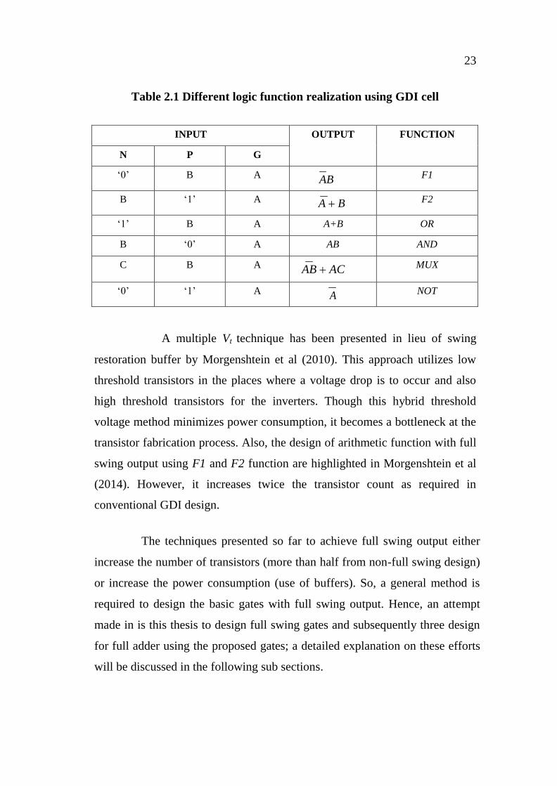
23
Table 2.1 Different logic function realization using GDI cell
INPUT OUTPUT FUNCTION
N P G
‘0’ B A
AB F1
B ‘1’ A A B F2
‘1’ B A A+B OR
B ‘0’ A AB AND
C B A AB AC MUX
‘0’ ‘1’ A
A NOT
A multiple Vt technique has been presented in lieu of swing
restoration buffer by Morgenshtein et al (2010). This approach utilizes low
threshold transistors in the places where a voltage drop is to occur and also
high threshold transistors for the inverters. Though this hybrid threshold
voltage method minimizes power consumption, it becomes a bottleneck at the
transistor fabrication process. Also, the design of arithmetic function with full
swing output using F1 and F2 function are highlighted in Morgenshtein et al
(2014). However, it increases twice the transistor count as required in
conventional GDI design.
The techniques presented so far to achieve full swing output either
increase the number of transistors (more than half from non-full swing design)
or increase the power consumption (use of buffers). So, a general method is
required to design the basic gates with full swing output. Hence, an attempt
made in is this thesis to design full swing gates and subsequently three design
for full adder using the proposed gates; a detailed explanation on these efforts
will be discussed in the following sub sections.

24
B B
B
B
B
2.2.1 Design of Gates using GDI Logic
The gates required for realizing any arithmetic function are AND,
OR, XOR and XNOR. These gate functions can be achieved with two
transistors (excluding the inverters for complementary input signals) and their
transistor level diagrams are shown in Figure 2.2.
GND
A A A
AND OR
A XOR
XNOR
B VDD
(a) (b) (c) (d)
Figure 2.2 GDI based gates (a) AND (b) OR (c) XOR and (d) XNOR
The operational characteristics of these gates are given in Table 2.2.
Assume both the inputs have voltage swing, then the output voltages are
subjected to different input combinations as given in Table 2.2.
Table 2.2 Operational characteristics of gates using GDI logic
INPUT LOGIC GATE
A B AND OR XOR XNOR
‘0’ ‘0’ |Vtp| |Vtp| |Vtp| VDD
‘0’ ‘1’ |Vtp| VDD VDD |Vtp|
‘1’ ‘0’ GND VDD-Vtn VDD-Vtn GND
‘1’ ‘1’ VDD-Vtn VDD-Vtn GND VDD-Vtn
25
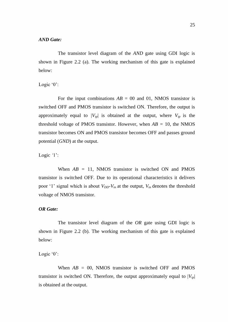
AND Gate:
The transistor level diagram of the AND gate using GDI logic is
shown in Figure 2.2 (a). The working mechanism of this gate is explained
below:
Logic ‘0’:
For the input combinations AB = 00 and 01, NMOS transistor is
switched OFF and PMOS transistor is switched ON. Therefore, the output is
approximately equal to |Vtp| is obtained at the output, where Vtp is the
threshold voltage of PMOS transistor. However, when AB = 10, the NMOS
transistor becomes ON and PMOS transistor becomes OFF and passes ground
potential (GND) at the output.
Logic ‘1’:
When AB = 11, NMOS transistor is switched ON and PMOS
transistor is switched OFF. Due to its operational characteristics it delivers
poor ‘1’ signal which is about VDD-Vtn at the output, Vtn denotes the threshold
voltage of NMOS transistor.
OR Gate:
The transistor level diagram of the OR gate using GDI logic is
shown in Figure 2.2 (b). The working mechanism of this gate is explained
below:
Logic ‘0’:
When AB = 00, NMOS transistor is switched OFF and PMOS
transistor is switched ON. Therefore, the output approximately equal to |Vtp|
is obtained at the output.

26
Logic ‘1’:
When AB = 01, PMOS transistor is switched ON and NMOS
transistor is switched OFF. Therefore, VDD passes through PMOS transistor.
On the contrary, the case occurs when AB = 10 and 11. In this case NMOS
turns ON and PMOS turns OFF resulting in poor ‘1’ signal in NMOS which is
about VDD-Vtn at the output.
XOR Gate:
The transistor level diagram of the XOR gate using GDI logic is
shown in Figure 2.2 (c). The working mechanism of this gate is explained
below:
Logic ‘0’:
When AB = 00, NMOS transistor is switched OFF and PMOS
transistor is switched ON. Therefore, the output obtained is approximately
equal to |Vtp|. However, when AB = 11, the NMOS transistor becomes ON and
PMOS transistor becomes OFF and passes ground potential (GND) at the
output.
Logic ‘1’:
When AB = 01, PMOS transistor is switched ON and NMOS
transistor is switched OFF. Therefore, VDD passes through PMOS transistor.
On the contrary, the case occurs when AB = 10. In this case NMOS turns ON
and PMOS turns OFF resulting in poor ‘1’ signal in NMOS which is about
VDD-Vtn at the output.
XNOR Gate:
The transistor level diagram of the XNOR gate using GDI logic is
shown in Figure 2.2 (d). The working mechanism of this gate is explained
below:

27
Logic ‘0’:
When AB = 01, NMOS transistor is switched OFF and PMOS
transistor is switched ON. Therefore, the output is approximately equal to|Vtp|.
However, when AB = 10, the NMOS transistor becomes ON and PMOS
transistor becomes OFF and passes ground potential (GND) at the output.
Logic ‘1’:
When AB = 00, PMOS transistor is switched ON and NMOS
transistor is switched OFF. Therefore, VDD passes through PMOS transistor.
On the other hand, when AB = 10, NMOS turns ON and PMOS turns OFF
resulting in poor ‘1’ signal in NMOS which is about VDD-Vtn at the output.
From this discussion, it is concluded that the output voltages are
degraded by threshold voltage drop for certain input combinations. The
reduction in output voltage increases significantly with increase in number of
stages. Therefore, the design of full swing gates is necessary and it is
discussed in the forthcoming subsections.
2.2.2 Full Swing AND, OR, XOR and XNOR Gates
The placement of additional PMOS or NMOS transistor at the
output depends on voltage VDD or GND potential, respectively which mitigates
the non full swing problems existed in the conventional scheme. The
transistor level schematics of the proposed gates are illustrated in Figure 2.3
and brief representations of their operational characteristics are given in Table
2.3.

28
Figure 2.3 Proposed full swing gates using GDI logic (a) AND (b) OR (c)
XOR and (d) XNOR
The operation of proposed gates is explained as follows: The
existing design lacks in full swing operation for particular input combinations.
The techniques presented in the literature directly use supply rail VDD for
strong ‘1’ and GND for strong ‘0’. But the proposed design does not use
supply rails either GND or VDD for obtaining the perfect output. It uses input,
but only with proper biasing of a necessary transistor, which may be either
PMOS or NMOS. This in turn would depend on the input level, to mitigate
the threshold voltage loss, which occurs in conventional design.
B
GND
A
A
AND
P1
N1
N2
B
A
A
OR
P1
N1P2
(a) (b)
B
A
B
A
A
B
XOR
P1
P2N1
N2
B
A
B
A
A
XNOR
P1
P2N1
N2
B
(c) (d)

29
Table 2.3 Operational characteristics of the proposed full swing GDI
gates
INPUT LOGIC GATE
A B AND OR XOR XNOR
0’ ‘0’ GND GND GND VDD
‘0’ ‘1’ GND VDD VDD GND
‘1’ ‘0’ GND VDD VDD GND
‘1’ ‘1’ VDD VDD GND VDD
AND Gate:
The transistor level diagram of the proposed full swing AND gate is
shown in Figure 2.3 (a). The working mechanism of this gate is explained
below:
Logic ‘0’:
For the input combinations AB = 00 and 01, N1 (NMOS) transistor is
switched ON and P1 (PMOS) and N2 (NMOS) transistors are switched OFF.
Therefore, the output node is connected to GND potential through N1.
Likewise for another input condition AB = 10, N1 transistor becomes switched
OFF and P1 (PMOS) and N2 (NMOS) transistors are switched ON. Though
P1 and N2 are ON state, N2 will be responsible for delivering GND potential at
the output.
Logic ‘1’:
When AB = 11, N1 (NMOS) transistor is switched OFF, whereas,
P1 (PMOS) and N2 (NMOS) transistors are switched ON, due to the
operational characteristics of P1 it delivers VDD value at the output.

30
OR Gate:
The transistor level diagram of the proposed full swing OR gate is
shown in Figure 2.3 (b). The working mechanism of this gate is explained
below:
Logic ‘0’:
When AB = 00, transistor P2 and N1 will be switched ON whereas
the drain terminal of N1 is connected to GND potential. It is interesting from
the operational characteristics of NMOS, it is good at delivering strong ‘0’
i.e., GND at the output. Therefore, the non full swing problem occurred in the
conventional GDI gate is eliminated.
Logic ‘1’:
For the input combination AB = 01, the transistors N1 and P2 will be
switched ON and the output terminal is tied to VDD potential through P2
transistor. Likewise when AB = 10 and 11, P1 transistor alone will be
switched ON and the output terminal is charged to the potential of VDD
through the same transistor .
XOR Gate:
The transistor level diagram of the proposed full swing XOR gate is
shown in Figure 2.3 (c). The working mechanism of this gate is explained
below:

31
Logic ‘0’:
When AB = 00, P1 and N2 will be switched ON and other two
transistors namely, P2 and N1 will be switched OFF. The output node is
connected to GND potential through N2 transistor. On the other hand, for the
input combination of AB = 11, N1 transistor becomes switched ON and the
remaining transistor are switched OFF. The output node is tied to GND
potential.
Logic ‘1’:
When AB = 01, the transistors P1 and P2 will be switched ON
whereas N1 and N2 will be switched OFF state. It is well known that PMOS
transistor is good at delivering strong ‘1’ potential (VDD). Likewise, for
another input combination AB =10, the transistor P2 and N1 will be switched
ON and the delivering of VDD potential is taken care by the PMOS transistor
P2.
XNOR Gate:
The transistor level diagram of the proposed full swing XNOR gate
is shown in Figure 2.3 (d). The working mechanism of this gate is explained
below:
Logic ‘0’:
When AB = 01, P1 and N2 transistors are switched ON and passing
GND potential to the output is performed by N2 transistor. Likewise, when AB
= 10, N1 and P2 transistors are switched ON, the source of N1 is connected to
the input B i.e. GND potential. Therefore, the output node is tied at GND
potential.

32
Logic ‘1’:
When AB = 00, the transistor P1 will be switched ON. The output
node is connected to VDD potential through P1 transistor since its drain
terminal is tied to inverted input B i.e. VDD. Another input combination AB =
11 drives the transistor N1, N2 and P2 into ON state. The delivering of VDD
potential to the output terminal will be done by P2 transistor.
2.3 FULL ADDER DESIGNS
The design of GDI full adder with full swing output can be made
possible with the help of full swing gates such as AND, OR, XOR and XNOR
discussed in the previous section. This design completely eliminates the swing
restoration buffers that results in improvement in the performance. Three
possible full swing GDI full adders are designed based on the design’s
expressions [eqs. (2.1) - (2.6)] and their schematic diagrams are given in
Figure 2.4.
Design 1:
The transistor level schematic of full adder using design 1 is shown
in Figure 2.4 (a). The Sum and Cout expressions of this full adder are given in
eqs. (2.1) and (2.2), respectively.
(2.1
(2.2
Design 1 uses XOR output as an intermediate result for computing
Sum and Cout. Sum output can be attained by multiplexing the XOR and its
inverted version XNOR through Cin input. The Cout is obtained by multiplexing
the inputs A and Cin whose output is controlled by the selection input, i.e. XOR
output of A and B inputs. The presence of inverter on the

33
critical path increases the delay of the whole circuit. This design is simple and
requires a total of 18 transistors for realizing the full adder function.
Design 2:
The Sum and Cout expressions of the design 2 are represented in eqs.
(2.3) and (2.4), respectively. This design can be attained by means of XOR,
AND and OR along with multiplexer modules.
(2.
(2.4
Multiplexing the AND and OR operation through carry input Cin
helps in Cout realization. The XOR operation on the inputs A, B and Cin
achieves Sum function. It uses total 22 transistors for implementing Design 2
full adder. The schematic of this full adder is given in Figure 2.4 (b).
Design 3:
This full adder is designed with the help of XOR, AND and OR
gates. and the output expressions of Sum and Cout are given in eqs. (2.5) and
(2.6).
(2.
(2.
In this design, Sum output can be achieved by XORing the inputs A,
B and Cin whereas the output Cout is obtained with the help of AND and OR
followed by XOR gate. The intermediate XOR gate output is used for
computing Sum and Cout outputs. The total transistor requirement of this full
adder is 23. The schematic representation of this full adder is given in Figure
2.4 (c).

34
Figure 2.4 Schematic of the proposed full adders based on (a) Design 1
(b) Design 2 and (c) Design 3
Cin
Cin
B
A
B
A
A
B
Cin
Cin
SUM
A
Cin
Cout
(a)
B
A
B
A
A
B
Cin
Sum
Cin
Cin
B
GND
A
A
B
A
A
C
Cin CoutCin
VDD
(b)
B
A
B
A
A
B
Cin
Sum
Cin
Cin
B
GND
A
A
GND
Cin
Cin
AB CoutAB
(c)

35
2.4 RESULTS AND DISCUSSION
In this thesis, full swing gates are proposed and their performance
shall be compared to the existing works. Further, three GDI full adders are
designed based on those full swing gates and their performances are also
compared to other adders found in the literature in terms of speed of
operation, power consumption and layout area. SPICE simulations are
performed in 45 nm technology with VDD = 1.1V. Typical transistor sizes, i.e.,
(W/L)p=240 nm/45 nm and (W/L)n=120 nm/45 nm are used. After the
completion of simulation of 42C, the layout is generated for each of them and
subjected to Design Rule Check (DRC) then Layout Versus Schematic (LVS)
check before the extraction of parasitic. Subsequently, the extracted parasitic
file is back annotated to perform the post layout simulation.
2.4.1 Performance Analysis of AND, OR, XOR and XNOR Gates
The simulation results of the proposed full swing gates along with
the existing designs are shown in Table 2.4. The performance parameters of
the gates namely, delay and power consumption are calculated from the
simulation. The area is measured from the obtained layout.
Table 2.4 Performance comparison of the proposed gates with existing
designs
Design Delay (ps) Power Consumption
(nW)
Area (µm2)
AND OR XOR XNOR AND OR XOR XNOR AND OR XOR XNOR
Ref. [172] 13.3 11.2 23.2 20 350 295 547 514 3.53 3.7 4.6 7.3
Ref. [93] 7.8 8.8 22 25.2 309 259 403 464 2.9 3.0 4.2 4.1
Proposed
(This
Work)
7.4
4.8
7.5
9.4
277
227
284
339
2.2
2.3
3.2
3.4

36
AND Gate:
The simulation results of the AND gate based on CMOS, GDI and
proposed are given in Table 2.4. The proposed AND gate operates with shorter
delay which is achieved with the help of reduced transistor count in the design.
Due to inherent property of low power consumption of GDI logic, the
proposed gate operates with less power consumption. The power saving
attained in this design compared with CMOS and GDI is 21% and 10%,
respectively. Due to the merit of less number of transistors, the designed gate
consumes 38% and 24% less area than CMOS and GDI based gate
respectively. The layout of the proposed gate is shown in Figure 2.5.
Figure 2.5 Layout of the proposed AND gate

37
OR Gate:
The performances of the proposed OR gate in terms of delay and
power consumption is analyzed through simulation and they are compared
with existing design results. From the results, it is understood that the
proposed design outperforms the existing design. The power saving is
accomplished by the proposed design is 23% and 12% more than CMOS and
GDI based design, respectively. Though GDI logic operates with low power
consumption, the use of buffer increases the power consumption whereas in
CMOS logic the increased switching activities might be responsible for
increased power consumption. While considering layout area, the proposed
design has occupied 38% and 23% less area than CMOS and GDI based
realization of the same design. The layout of the proposed OR gate is shown
in Figure 2.6
Figure 2.6 Layout of the proposed OR gate

38
XOR Gate:
The XOR gate based on GDI and proposed performs better in all
aspects than CMOS based design. The delay improvement in the proposed
XOR gate is 66% more than GDI which is resulted from the elimination of
buffer in the output path. On the other hand, the XOR gate based on CMOS
has large input capacitance which results into the slowdown of the operation.
With respect to power consumption, the proposed XOR gate operates at least
rates since it has no direct path between the power supply and ground rails,
which eliminates direct short circuit current. The power saving possible by the
proposed design is 48% and 30%, respectively more than CMOS and GDI
based implementation of the same. The transistor count is also reduced
compared with the other full swing XOR gates reported in the literature which
in turn reduces the overall layout area. The area minimization in proposed
XOR gate is 30% and 24%, respectively more than CMOS and GDI based
design.
Figure 2.7 Layout of the proposed XOR gate

39
XNOR Gate:
Among the simulated XNOR gate designs, the proposed XNOR
performs better in terms of delay, power consumption and area. The delay
improvement in the proposed XNOR gate is 53% and 62%, respectively more
than GDI and CMOS based realization. Due to the elimination of supply rails
in the circuit, the overall power consumption of the proposed XNOR gate has
been lowered. The proposed XNOR gate consumes 34% less power than
CMOS based design. Likewise, the transistor count is also reduced compared
to the existing designs found in the literature [93]. While considering the
layout area, proposed XNOR gate saves 53% and 17%, respectively more than
CMOS and GDI based implementation.
Figure 2.8 Layout of the proposed XNOR gate
40
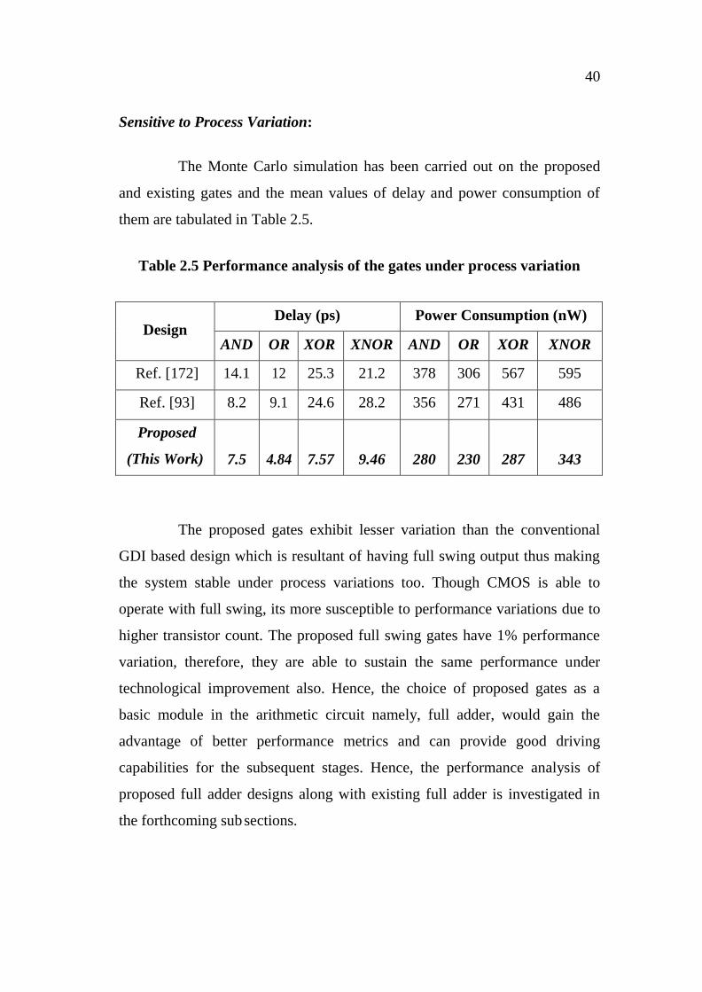
Sensitive to Process Variation:
The Monte Carlo simulation has been carried out on the proposed
and existing gates and the mean values of delay and power consumption of
them are tabulated in Table 2.5.
Table 2.5 Performance analysis of the gates under process variation
Design
Delay (ps) Power Consumption (nW)
AND OR XOR XNOR AND OR XOR XNOR
Ref. [172] 14.1 12 25.3 21.2 378 306 567 595
Ref. [93] 8.2 9.1 24.6 28.2 356 271 431 486
Proposed
(This Work)
7.5
4.84
7.57
9.46
280
230
287
343
The proposed gates exhibit lesser variation than the conventional
GDI based design which is resultant of having full swing output thus making
the system stable under process variations too. Though CMOS is able to
operate with full swing, its more susceptible to performance variations due to
higher transistor count. The proposed full swing gates have 1% performance
variation, therefore, they are able to sustain the same performance under
technological improvement also. Hence, the choice of proposed gates as a
basic module in the arithmetic circuit namely, full adder, would gain the
advantage of better performance metrics and can provide good driving
capabilities for the subsequent stages. Hence, the performance analysis of
proposed full adder designs along with existing full adder is investigated in
the forthcoming sub sections.

41
2.4.2 Performance Analysis of Full Adder
Full adders based on CMOS, CPL, hybrid logic and GDI are
compared to the proposed designs. CMOS logic consists of 28 transistors,
which is considered as reference for comparison. It has a full voltage swing
with buffered Sum and Cout signals. CPL, which is a variant of PTL uses 32
transistors and provides both complementary and true output of Sum and Cout
signals. It uses the feedback transistors for providing full swing. A design
which uses a combination of CMOS and PTL to generate Sum and Cout,
respectively is called hybrid design. For all possible input combinations
applicable to the full adder, the average power consumption and worst case
delay are measured. Table 2.6 summarizes the simulation results of single full
adder. The delay is measured by accounting the time taken from 50% of the
input voltage swing to 50% of the output voltage swing on each transition.
The maximum delay is treated as worst case delay.
From the results of Table 2.6, it is very clear that CPL logic
consumes relatively more power due to more number of transistors required
for its design. In the case of hybrid design, this equally performs well with
CMOS in terms of delay and power consumption. However, it takes lower
number of transistor count compared to CMOS for its design, whereas the
three proposed GDI based full adders, especially Design 2 outperforms all the
other adders in both delay and PDP. This would have resulted due to reduced
transistor count on the paths between input and output. This will also lead to
decrease in parasitic capacitance at the Sum and Cout nodes.

42
Table 2.6 Performance comparison of the proposed full adders with
existing designs
Design Delay
(ps)
Power
Consumption (nW)
Area
(µm2)
PDP
(e-18
J) Ref. [117] 46.2 975.6 22.1 45.1
Ref. [45] 38.8 2680 25.0 103.9
Ref. [168] 35.21 1613 18.0 56.8
Ref. [93] 41.3 1310 16.0 54.1
Ref. [164] 49.13 1685 15.6 82.7
Ref. [94] 32.2 1462 18.6 47.1
Design 1 37.86 927.9 10.1 35.1
Design 2 26.87 1140 13.4 30.6
Design 3 36.57 1216 14.6 44.4
The area overhead of the three proposed adders is lower than that of
conventional CMOS, CPL and hybrid adders taken for comparison. The
performance metrics of all the simulated adders such as delay, power
consumption, energy consumption and process variation analysis are
discussed elaborately in this sub sections.
Delay:
The delay results of the simulated adders are given in Table 2.6.
Among all three proposed adder designs, Design 2 has the lowest delay since
Cout and Sum are computed in parallel. Also the improved delay in Design 2
would have been a result of better driving capability of the proposed XOR
gate. The adder design based on Design 2 operates faster by 34.9% 45.3% and
16.5%, respectively better than the adder discussed in [93], [164] and [94].
The presence of inverter in the critical path of Design 1 leads the design to

43
have higher delay among the three proposed full adder. However, the Design
3 in terms of delay stands midway between Design 1 and Design 2 of the
proposed full adder.
The full adder discussed in [93] has longer delay than all other
designs taken for comparison. The low output voltage at internal nodes of full
adder based on XOR in [93] causes less driving capability resulting in longer
delay. Though the design discussed in [164] operates at full swing, the
presence of buffer in the critical path slowed down the operation. The adder
based on F1 and F2 gates in [94] reduced the delay compared to [93] and
[164] at the cost of more transistor count. However, the speed is still lower
than the proposed adder Design 2.
Power Consumption:
The power consumed by the adders are computed through
simulation and also presented in Table 2.6. It reveals that the three proposed
adders consume low power. Among the proposed adders, Design 1 consumes
low power since it adopts the proposed XOR gate and requires minimum
transistor count than the other two proposed designs. Even though their power
consumption is slightly higher than Design 1 they are still lower than other
existing adders except CMOS based adder. The percentage of power savings
attained with Design 1 is higher than adders explained in [93], [164] and [94]
by 29.2, 44.9 and 36.5, respectively.
Area:
The area of the designed and existing full adders is calculated from
their corresponding layout. For an understanding, the layouts of the proposed
three full adders namely, Design 1, Design 2 and Design 3 are given in Figure
2.9 (a), (b) and (c), respectively. Among the three proposed designs, Design 1
reports the smallest area. This saving has been obtained by partial sharing of

44
architecture between Sum and Cout output. Along with that, the removal of
buffers at the gate output results in transistor count reduction and
subsequently layout area too. The area occupied by Design 1 is 54% smaller
than CMOS based implementation as discussed in [117].
Power Delay Product (PDP):
From the simulation results given in Table 2.6, it is observed that
three proposed full adders consume only a small amount of energy (power
delay product) which is possible due to the presence of full swing gates in
those designs. These gates will only switch the required transistor for the
particular input. Hence, they consume less energy. Among the designs taken
for simulation, Design 2 operates on significantly lower energy consumption.
The amount of energy saving can be achieved with Design 2 is 32.1%, 70.5%
and 46.1% more than adder discussed in [117], [45] and [68], respectively.
The adder discussed in [164] provides full swing only at the output
stage owing to the buffering whereas the intermediate nodes suffered by
voltage drop like adder discussed in [93]. Therefore, the energy consumption
of the adder increases significantly. With respect to full adder based on F1
and F2 gates in [94], though it mitigates threshold drop at intermediate nodes,
the overall energy consumption is high due to more transistor count required
for design as shown in Table 2.6. The PDP of Design 2 is better than all other
designs.

45
(a)
(b)
(c)
Figure 2.9 Layouts of the proposed full adders based on (a) Design 1
(b) Design 2 and (c) Design 3
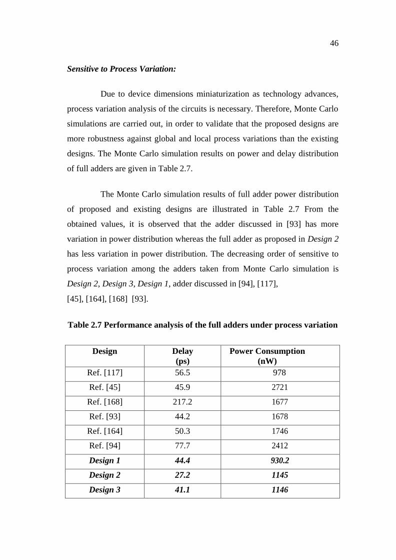
46
Sensitive to Process Variation:
Due to device dimensions miniaturization as technology advances,
process variation analysis of the circuits is necessary. Therefore, Monte Carlo
simulations are carried out, in order to validate that the proposed designs are
more robustness against global and local process variations than the existing
designs. The Monte Carlo simulation results on power and delay distribution
of full adders are given in Table 2.7.
The Monte Carlo simulation results of full adder power distribution
of proposed and existing designs are illustrated in Table 2.7 From the
obtained values, it is observed that the adder discussed in [93] has more
variation in power distribution whereas the full adder as proposed in Design 2
has less variation in power distribution. The decreasing order of sensitive to
process variation among the adders taken from Monte Carlo simulation is
Design 2, Design 3, Design 1, adder discussed in [94], [117],
[45], [164], [168] [93].
Table 2.7 Performance analysis of the full adders under process variation
Design Delay
(ps)
Power Consumption
(nW)
Ref. [117] 56.5 978
Ref. [45] 45.9 2721
Ref. [168] 217.2 1677
Ref. [93] 44.2 1678
Ref. [164] 50.3 1746
Ref. [94] 77.7 2412
Design 1 44.4 930.2
Design 2 27.2 1145
Design 3 41.1 1146
47
The Monte Carlo simulation results for delay distribution of
proposed and the existing full adders are given in Table 2.7. With reference to
performance variation, the decreasing order of delay variation, due to process
changes, among the simulated designs is Design 2, adder based on [164],
[117], Design 1, adder explained in [94], Design 3, adder given in [93], [45]
and [168]. From the values of delay distribution, the full adder based on F1
and F2 gates [94] has higher sensitive to process variation than CMOS based
design. It is observed from the delay distribution results, the full adder based
on [168] has more variation and the Design 2 adder has lower variation. It can
be concluded that Design 2 adder has higher immunity to process variation in
both delay and power distribution.
Three proposed full adder designs have advantages but also some
limitations. Design 1 is an optimal candidate for the applications in which
minimum transistor count and low power are important aspect of design
requirement. The Design 2 provides lower PDP and minimum delay, so it can
be suitable for battery operated and real-time applications. It has slightly
higher transistor count compared to Design 1. Design 3 lies midway between
Design 1 and Design 2, and offers lower delay than Design 1. From the
obtained results, it can be concluded that all three designs operate on low
energy consumption than existing adders taken for comparison. Hence, these
designs can be suitable candidates for realizing energy efficient arithmetic
applications.
2.5 SUMMARY
In this chapter, the digital gates namely, AND, OR, XOR and XNOR
are designed with low delay, low power consumption and small area with the
help of full swing GDI logic. Based on these gates, three full adder designs
that use as few as twenty transistors per bit are proposed. The design adopts
proposed full swing gates to alleviate the threshold voltage problem and to
48
enhance the driving capability for cascaded operation. The enhanced driving
capability also facilitates lower voltage and faster operation which leads to
lower energy consumption. The proposed designs along with existing adder
circuits are simulated using the SPICE simulation tool at 45 nm technology.
The comparison is done in terms of power consumption, propagation delay,
area and PDP. The proposed three designs have lower energy consumption
when compared to other designs presented in the literature. The process
variation analysis of circuits is studied through Monte Carlo simulation. From
the Monte Carlo simulation results, it is found that proposed adder based on
Design 2 can operate reliably and has higher tolerance against process
variation than the previously reported adder in the literature. Hence, these
proposed designs may be suitable for low energy and high speed VLSI circuit
applications.

49
CHAPTER 3
AREA AND ENERGY EFFICIENT 4-2 COMPRESSOR
DESIGN USING GDI LOGIC
3.1 INTRODUCTION
A fast multiplier is an essential component in any high performance
system. Compressors are building blocks of fast tree multiplier. Various
designs of compressors such as 42C, 5-2 and 7-3 have been introduced to
improve a multiplier speed. Among them, 42C is used in the multiplier partial
products reduction phase due to its regular structure. From the study of
various compressors, it is understood that 42C has better compression ratio
and can be considered as a replacement for carry save adder, which is
traditionally used in partial products reduction stage. Furthermore, the regular
structure of 42C decreases the interconnection complexity in the existing
Wallace and Dadda multipliers.
A straightforward realization of 42C uses two cascaded full adder
and has 4 gates delay. To address this issue, dedicated carry generation circuit
has been introduced in 42Cs and their architectures are well explored.
However, these 42Cs architectures exhibit hardware redundancy. Moreover,
the power consumption of redundant gates is not negligible which increases
the overall power consumption of 42C. This problem can be addressed by the
removal of redundant gates, which is accomplished by simplification of
compressor output Boolean expression without affecting its functionality. The
spurious switching activities, contributed by the redundant gates, are eliminate

50
in the proposed 42C thus resulting in power consumption minimization.
Further, the new design shall be proposed and implemented using GDI logic
in this thesis. The rest of the Chapter is organized as follows: Section 2
overviews on the existing 42C designs whereas in Section 3 will propose 42C
and its implementation using GDI logic. Further, the simulation results and
discussion of the 42C are given in Section 4 and finally, the summary is
drawn in Section 5.
3.2 RELATED WORKS OF 4-2 COMPRESSOR
Owing to its regular interconnection, 42C plays an important role in
a multiplier design. It receives x1, x2, x3, x4 and ci, five input bits of the same
weight, compresses them, and generates three output bits namely, s, co and c.
The output carry co is generated based on three inputs x1, x2 and x3 thus in the
results there are no horizontal carry propagation across the compressor. The
block diagram and the base architecture representation of 42C are shown in
Figures 3.1 (a) and 3.1 (b), respectively. The fundamental equation governs
the 42C operation can be reproduced as follows:
1 2 4 i 2 ( .1
4-2 Compressor
x1 x3 x2 x4 ci
sc
co
FA
x1 x2 x3
FA
x4 ci
co
c s
(a) (b)
Figure 3.1 42C (a) Block diagram and (b) Base architecture

51
The 42C functionality can be described in the following eqs. (3.2) - (3.4).
1 2 4 i (3.2)
co 1 2 ( 1 2 1 (3.3)
(3.4)
Conventionally, the 42C is implemented by two cascaded
connection of full adder cell, but it has a longer delay of 4 XOR gates. To
reduce this latency, variant 42Cs are developed with dedicated carry
generation circuits. The first dedicated carry generation circuit in 42C design
is introduced by Nagamatsu et al (1990). This design uses 3 XORs, 3 ANDs, 3
NORs and 1 inverter for carry computation and claims that delay reduced
significantly. Despite the advantages, the transistor count is more than that of
the conventional design. This gate count is reduced into 2XORs, 1NAND,
1NOR, 1MUX and 1 inverter in the 42C design, discussed by Oklobdzija
(1999).
Another method of the realization of carry computation in 42C,
performed by NAND and OR, which is designed by Hussin et al (2008), and
requires 2 XORs, 3 NANDs, 1 OR and 1 inverter. The XOR based intermediate
output computation, involved in previously discussed 42C designs, is replaced
with the help of NOR and NAND gates, discussed by Pishvaie et al (2013).
The drawback of this 42C is not only more power consumption due to
spurious switching activities and also more transistor count. The advantage of
partial utilization of CMOS full adder along with the gates while
implementing 42C architecture is discussed by Pishvaie et al (2012). They
also analyzed the performance of 54 bit multiplier using the designed
compressor. Though the design gains advantages in terms of speed and power
consumption it is suffered by increased area.

52
From the discussion on 42C, it is understood that the conventional
designs exhibit hardware redundancy due to the usage of separate circuits
while computing 42C sum and carry outputs. Moreover, this redundant
hardware increases transistor count and power consumption. This problem
can be addressed by simplifying compressor output Boolean expression
without affecting its functionality. From the truth table of the 42C, it is
observed that the carry output is same as carry input, if XOR output of ci and
x4 is low, otherwise, it follows the x1 x2 x3 output, where x1, x2, x3, x4
and ci are 42C inputs. This feature will be exploited in the proposed 42C,
which helps to use the partial sum output for carry computation. This
eliminates hardware duplication and thus reduces overall transistor count. In
addition to that, the elimination of unnecessary circuits, which might be a
reason for spurious switching activities, would result in reduction of total
power consumption of proposed 42C.
To implement the building blocks of new 42C, GDI logic is chosen.
This logic helps to implement proposed architecture with merits of low power
consumption and lower transistor count compared to other logic styles
namely, CMOS, PTL and transmission, which are used in the existing 42C
designs. Moreover, the existing design prefers either PTL/transmission, due to
its lesser transistor count, but their operational characteristics i.e. weak
driving ability is considered as a drawback. On whole, the proposed
compressor facilitates advantage in both simple architecture and
implementation (mitigates the weak driving problem which is encountered in
the existing 42C designs) level. The discussion on the proposed 42C and the
implementation using full swing GDI logic is explained in the forthcoming
Section.

53
3.3 METHODOLOGY
This Section discusses the architecture and operation of proposed
42C followed by its implementation using full swing GDI logic.
3.3.1 Proposed 4-2 Compressor
The hardware duplication found in the carry computation techniques
of conventional 42C designs is considered as a drawback at both architecture
and implementation level. This can be reduced by sharing the partial output of
sum computation into carry output also. In general, the sum output is obtained
by XOR operation of x1, x2, x3, x4 and ci, in serial. But in the proposed 42C, it
is portioned into two stages. In one stage it performs XOR operation of x1, x2
and x3 where as in another stage, the operation performs over x4 and ci, where
x1, x2, x3, x4 and ci are input bits. The first and second stage outputs are labeled
as M and N, respectively, which are given in eqs. (3.5) and (3.6). Also, it is
noted that both the stage computations are performed in a parallel manner.
Among the two intermediate M and N outputs, N output acts as a
select input for carry computation. If the select input (N) is zero, and then
carry output is same as carry input, otherwise, the carry output follows the
value of M. Further, the XOR operation of M and N will result into
compressor sum output. The sum and carry outputs are represented as s and c,
respectively, whereas co is denoted as a horizontal carry and it is computed
from multiplexing the inputs, either x1/x3 depending on the XOR output of x1
and x2.The proposed 42C’s outputs are expressed in the following eqs.(3.5) - (3.9).
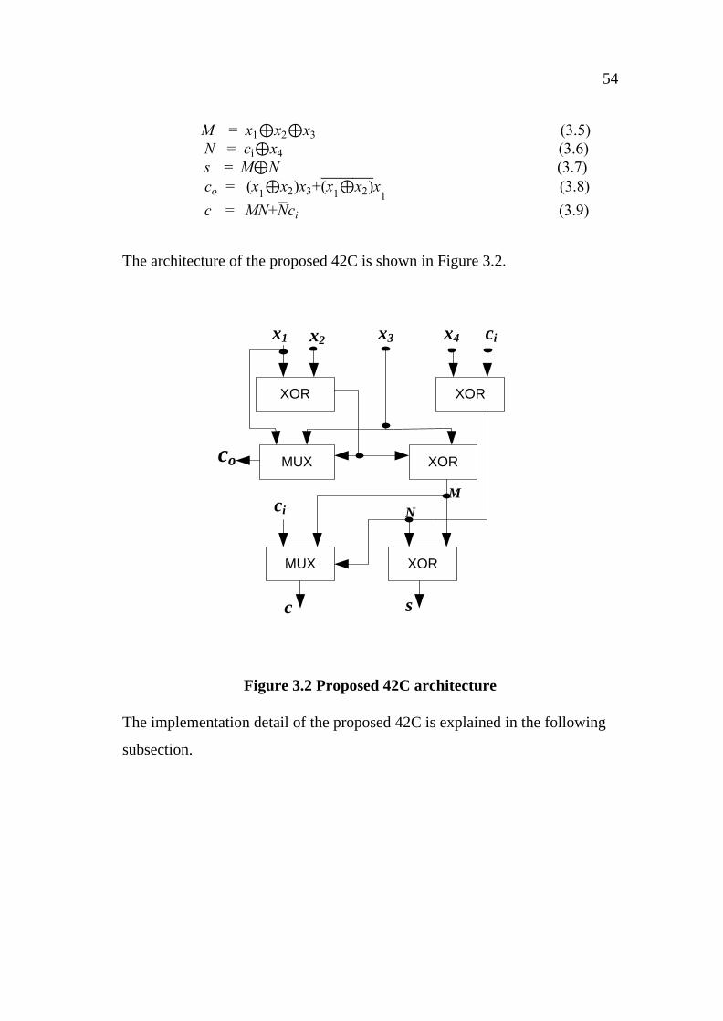
54
1 2 ( . i 4 ( . ( . ( 1 2 ( 1 2
1 ( .
( .
The architecture of the proposed 42C is shown in Figure 3.2.
XOR XOR
MUX XOR
MUX XOR
c
x1 x2 x4
s
cix3
co
ci
M
N
Figure 3.2 Proposed 42C architecture
The implementation detail of the proposed 42C is explained in the following
subsection.

55
3.3.2 GDI Logic
The performance of 42C is influenced by the performance of their
basic modules such as XOR and MUX. The implementations of XOR and
MUX using various logic styles namely, CMOS, PTL and transmission are
well explored in literature. In Abidi et al (2012), a study of performance
comparison of 42C with various logic styles is discussed and concluded that
each implementation performs well in one aspect while compromising other
aspects. The CMOS based implementation of 42C, discussed by Srinivas et al
(2007), has a good driving capability, but the need for more transistor count is
considered as a limitation.
A method of implementing 42C, which has sufficient driving
capability, with reduced transistor count, without increasing interconnection
complexity, is made possible with the help of GDI logic. The design of gates
with the full swing output using GDI logic is obtained through the placement
of additional PMOS or NMOS transistor at the output terminal depends on the
voltage degradation i.e. (VDD-Vt or Vtp). Based on this technique, a set of gates
and adders in GDI logic with full swing are designed and are well explored in
the previous Chapter. From their simulation results, it is understood that these
components exhibit better performance in terms of delay, power consumption
and area. Therefore, they can be used for realizing the proposed 42C to
improve the performance. The diagram of XOR and MUX using GDI logic is
shown in Figures 3.3 (a) and 3.3 (b), respectively.

56
Figure 3.3 GDI logic based (a) XOR and (b) MUX
3.4 RESULTS AND DISCUSSION
In this Section, the simulation results of the proposed and the
existing 42Cs are presented and their performance in terms of delay, power
consumption and layout area is compared. SPICE simulations have been
performed at 45 nm technology with a supply voltage (VDD) of 1.1 V. Typical
transistor sizes, i.e., (W/L)p=240 nm/45 nm and (W/L)n=120 nm/45 nm are
used. After the completion of simulation of 42C, the layouts have been
generated for each of them and are subjected to DRC then LVS check before
the extraction of parasitic. Subsequently, the extracted parasitic file is back
annotated to perform the post layout simulation. The simulation results of 42C
are given in Table 3.1.
Table 3.1 Performance comparison of the proposed 4-2 compressor
with existing designs
S. No. Design Delay
(ps)
Power Consumption
(µW)
Area
(µm2)
PDP
(e-18 J)
1 Ref. [112] 126 6.7 56 844
2 Ref. [107] 175 8.3 55 1452
3 Ref. [65] 137 6.9 58 945
4 Proposed
(This Work) 114 4.4 51 502
B
A
B
A
A
B
XOR
B
A
B
A
MUX
(a) (b)

57
Delay:
The delay is measured by accounting the time from the 50% of the
input voltage swing to 50% of the output voltage swing for each transition.
The maximum delay is treated as worst case delay. The delay computed
through simulation, for all the 42C structures are given in Table 3.1. As it is
expected, proposed 42C has smaller delay compared to those other existing
implementations. This is achieved due to parallel computation of intermediate
outputs. On the other hand, the design discussed in [107] has the highest
delay, due to the requirement of complementary signal imposed by this
compressor architecture. The speed improvement obtained by the proposed
42C is 35%, 17% and 10% more than that of 42Cs discussed in [107], [65]
and [112], respectively.
Power Consumption:
While designing any system, the minimization of power
consumption is given prime importance. In general, the circuit’s power
consumption is determined from their switching activities and node and wire
capacitances. The power consumed by the 42Cs are computed through
simulation and also presented in Table 3.1. The results indicate that the
architecture discussed in [107] and [65] have more power consumption than
that of design in [112] and proposed 42C. The minimum power consumption
is witnessed in proposed 42C owing to its simple and regular structure,
whereas the architecture in [107] consumes more power due to its dense
wiring tracks.
Area:
The layout is drawn for all the existing and proposed 42Cs. The area
is evaluated from their layout and it is given in Table 3.1. From the obtained

58
results, it is witnessed that proposed 42C has less area, whereas more area
belongs to the 42C discussed in [107]. As stated earlier, in Section 3, GDI
logic implements XOR and MUX with reduced transistor count. Therefore, the
area of the proposed 42C is lesser. The layout of the proposed 42C is shown
in Figure 3.4. The percentage of area reduction possible with proposed 42C is
about 9% more than that of a recently reported compressor in [112].
Figure 3.4 Layout of the proposed 42C

59
PDP:
The power delay product of the proposed and existing 42C designs
are given in Table 3.1. Among the compressors discussed, the best and the
worst PDP belong to 42C of proposed and the design discussed in [107],
respectively. The energy saving accomplished with proposed design is 41%
more than the compressor reported in [112]. It is examined from the obtained
results of PDP of 42Cs, the proposed design implemented with GDI logic, has
small PDP with acceptable speed and hence, it can be a proper choice while
performing partial products accumulation in the multiplier.
Sensitivity to Process Variation:
In order to evaluate the sensitivity of the designs to local and global
process variations, Monte Carlo simulations have been carried out and the
results are tabulated in Table 3.2.
Table 3.2 Performance analysis 4-2 compressors under process variation
S. No. Design Delay
(ps)
Power
Consumption (nW)
PDP
(e-18 J)
1 Ref. [112] 129 6855 0884
2 Ref. [107] 184 8506 1565
3 Ref. [65] 137 6811 0933
4 Proposed
(This Work)
115 4410 0507

60
As expected, proposed compressor design has better immunity to
process variation. Moreover, the design based on pass transistor gate,
discussed in [107] is more sensitive due to its driving current dependence on
process sensitive Vt, which is amplified due to voltage drops at internal nodes.
The PDP variation of the proposed design is 1%, whereas the existing
compressor explained in [112] shows about nearly 5%.
3.5 SUMMARY
In this Chapter, a new approach for the design of 4-2 compressor,
which is based on the modification of the existing compressor carry output
implementation without affecting its functionality, is presented. This
technique utilizes the partial output generated during sum computation, used
for carry output. The carry output is same as carry input if XOR operation of ci
and x4 is low otherwise, it follows the XOR output of x1, x2 and x3 input. To
accomplish this, the design divides the computation of sum into two stages
and it is allowed to perform the computation in parallel. The part of the sum
output acts as a select input while implementing carry output. This
modification eliminates hardware redundancy, which is exhibited in the
existing designs, to minimize the transistor count. Moreover, the spurious
transitions from the duplicate gates are avoided, which minimizes the overall
power consumption of the proposed 4-2 compressor significantly. Further, the
performance of 4-2 compressor is improved by proper implementation of
building blocks namely, XOR and MUX. The proposed and the existing 4-2
compressor designs are simulated using 45 nm technology model. The
comparison is done in terms of delay, power consumption, area and PDP. The
proposed design has shown 41% more improvement in PDP compared with
existing compressor reported in the literature. Hence, this area and energy
efficient compressor would be used as one of the building modules for the
implementation of multiplier in signal processing applications.

61
CHAPTER 4
PERFORMANCE IMPROVEMENT OF PARALLEL
ADDERS USING GDI LOGIC
4.1 INTRODUCTION
While the growth of electronics market has driven the VLSI
industry towards very high integration density and system on chip, critical
concerns have been arising on a severe increase in power consumption and
area. High power consumption raises temperature profile of the chip and
affects overall performance of the system. Moreover, the explosive growth in
laptops and portable personal communication systems demand long battery
life at the modest performance. This necessitates an intensive research in low
power and low area integrated circuit design.
Parallel adders are developed to minimize the delay involved in the
binary addition task and are well suited for VLSI implementation. The
performance of these adders can be greatly influenced by the performance of
their basic modules. In this chapter, an efficient implementation of parallel
adders using GDI logic is discussed. The parallel adders under consideration
are, ripple carry, carry select and carry look ahead adders. The basic modules
of these parallel adders are full adder (for (RCA)), XOR and AND gate (for
(CLA)), full adder and MUX (for (CslA)). Therefore, these basic modules are
realized using GDI logic. The organization of the Chapter is as follows:
Section 2 gives an overview of the parallel adders and its implementation
using GDI

62
logic. In Section 3, their simulation results and discussion are given and the
Section 4 summarizes this Chapter.
4.2 AN OVERVIEW OF PARALLEL ADDERS
A brief description of the parallel adders is given in the following
sub section.
4.2.1 Ripple Carry Adder
The RCA is O (n) time and O (n) area adders, where, n is the width
of the operands. General n bit RCA architecture is shown in Figure 4.1. In the
worst case, a carry can propagate from least significant bit position to the
most significant bit position. Moreover, one stage of the RCA, the single full
adder, determines the performance of RCA. Therefore, the delay of RCA can
be decreased by implementing using fast full adder. In order to achieve this
performance, a full adder based on GDI logic is chosen in this research work.
Further, the carry propagation delay can be reduced by minimizing carry
propagation path or by performing pre computation of carries.
FA FA FA FA
Critical Path
N-bit RCAFull Adder
S3
S2
S1
SN
A1
B1
A2
B2
A3
B3
AN
BN
Co
Ci
C1
C2
C3
C4
CN
Figure 4.1 N bit RCA architecture

63
4.2.2 Carry Look Ahead Adder
CLAs have become popular due to their high speed and modularity.
They are O (log n) time and O (n log n) area adders. Consider the n-bit
addition of two n- bit numbers A= an-1, an-2, an-3, .., a0 and B = bn-1, bn-2, bn-3…,
b0 resulting in the output sum S = Sn-1, Sn-2,.., S0 and carry out Cout.
The first stage in CLA computes the bit generate (Gi) and propagate
(Pi) as follows
= (4.1)
(4.2)
These are then utilized to compute the final sum (Si) and carry (Ci+1) bits.
(4.
(4.4)
Where 0 ≤ ≤ -1
An overall delay of carry look ahead adders is dominated by the
delay of passing the carry in look ahead stages. From the CLA architecture, it
is understood that its building blocks are XOR and AND gates. Moreover, the
CLA performance is determined from these basic gates performance.
Therefore, the performance improvement in CLA is possible by implementing
its building blocks using GDI logic.
4.2.3 Carry Select Adder
To minimize the delay due to carry propagation involved in RCA,
CslA is evolved, in which, two additions are performed in parallel, one
assuming Cin as 0 and other one as 1. When the carry is known, finally the
correct sum is selected. They are O (2n) area and O (√ ) time adders. CslA

64
has been used in many computational systems to alleviate the problem of
carry propagation delay by independently generating multiple carries and then
by selecting a final carry to generate the sum. However, CslA is not area
efficient because it uses multiple pairs of RCA to generate intermediate sum
and carry for Cin= 0 and Cin=1.
The different techniques for minimizing the use of dual RCA in
CslA have been attempted by (Ramkumar and Kittur 2012 and Mohanty and
Patel 2014). An interesting approach discussed by Ramkumar and Kittur
(2012) is the use of Binary to Excess 1 Converter (BEC) instead of RCA for
Cin=1. The BEC based CslA involves less logic resources than the
conventional CslA. Also, the area reduction is possible in CslA with the
technique of sharing common Boolean logic expression for Cin 0 and 1
(Youngjoom Kim and Lee-Sup Kim 2001). Though this technique requires
less logic resources than the BEC based CslA, the carry propagation delay
generated is longer. Further, CslA design is simplified based on logic
reformulation and optimization of carry generator module which is explained
by Mohanty and Patel (2014). This design possesses smaller area and delay
than the conventional CslA design. However, still the performance of CslA
design can be improved by proper implementation of their basic modules such
as MUX and full adder. Therefore, the CslA is implemented based on the
proposed designs as discussed in Chapter 2 of this thesis.
4.3 RESULTS AND DISCUSSION
In this Section, the simulation results of the parallel adders based on
CMOS, GDI and proposed are presented and their performance will be
compared. During the evaluation of these adders, the performance metrics
such as area, delay, power consumption and PDP are taken into account.
SPICE simulations are performed at 45 nm technology with a supply voltage
(VDD) of 1.1 V. Typical transistor sizes, i.e., (W/L)n=120 nm/45 nm and
(W/L)p=240 nm/45 nm are used. After the completion of simulation of
parallel adders, the layout is generated for each of them and is subjected to

65
DRC and then LVS check before the extraction of parasitic. Subsequently, the
extracted parasitic file is back annotated to perform the post layout simulation.
Delay:
The delay is measured by accounting the time from the 50% of the
input voltage swing to 50% of the output voltage swing on each transition.
The maximum delay is treated as worst case delay. The delay is computed
through simulation for all the adder structures are given in Figure 4.2 (a). As
it is expected, CLA structures have smaller delay compared to those other
four adders due to the parallel computation of their carries. On the other hand,
RCA has the highest delay due to its serial structure. However, RCA
implemented based on proposed adder, discussed in the Chapter 2 of this
thesis, has shown 12% and 6% speed improvement than CMOS and GDI
adders, respectively. The critical path delay of CslA is smaller than that of
RCA due to the skipping of carry propagation. The implementation of CslA
discussed in [172], [125] and [89] through the use of proposed gates achieves
delay reduction of 15%, 27% and 20% more than CMOS based
implementation of those adders.
Power Consumption:
Power is one of the vital sources hence a major attention is paid to
minimize the power consumption while designing the system. It mainly depends
on the switching activities and node and wire capacitances. The power
consumed by the parallel adders are computed through simulation and also
given in Figure 4.2 (b). The results indicate that the CLA and CslA have higher
power consumption than that of RCA. The minimum power consumption is
witnessed in RCA owing to its simple and regular structure while CLA
consumes more power due to its dense wiring tracks. However, the power
consumption of the CLA based on proposed gates is reduced by 30% than
CMOS based design.

66
Figure 4.2 Performance comparison of parallel adders (a) Delay (b)
Power Consumption (c) Area and (d) PDP
(a)
(b)
(c)
(d)
0
200
400
600
800
1000
1200
CMOS (Ref. [172]) GDI (Ref. [94]) Proposed (This Work)
De
lay
(ps)
RCA (Ref. [27])
Conventional CslA (Ref. [172]) BEC CslA (Ref. [125])
Modified CslA (Ref. [89])
CLA (Ref. [94])
0
100
200
300
400
CMOS (Ref. [172]) GDI (Ref. [94]) Proposed (This Work)
Po
we
r C
on
sum
pti
on
(µ
W) RCA (Ref. [27])
Conventional CslA (Ref. [172])
BEC CslA (Ref. [125])
Modified CslA (Ref. [89])
CLA (Ref. [94])
0
500
1000
1500
2000
2500
3000
CMOS (Ref. [172]) GDI (Ref. [94]) Proposed (This Work)
Are
a (µ
m2 )
RCA (Ref. [27])
Conventional CslA (Ref. [172])
BEC CslA (Ref. [125])
Modified CslA (Ref. [89])
CLA (Ref. [94])
0
20
40
60
80
100
120
CMOS (Ref. [172]) GDI (Ref. [94]) Proposed (This Work)
PD
P (
e -
15
J)
RCA (Ref. [27])
Conventional CslA (Ref. [172])
BEC CslA (Ref. [125])
Modified CslA (Ref. [89])
CLA (Ref. [94])
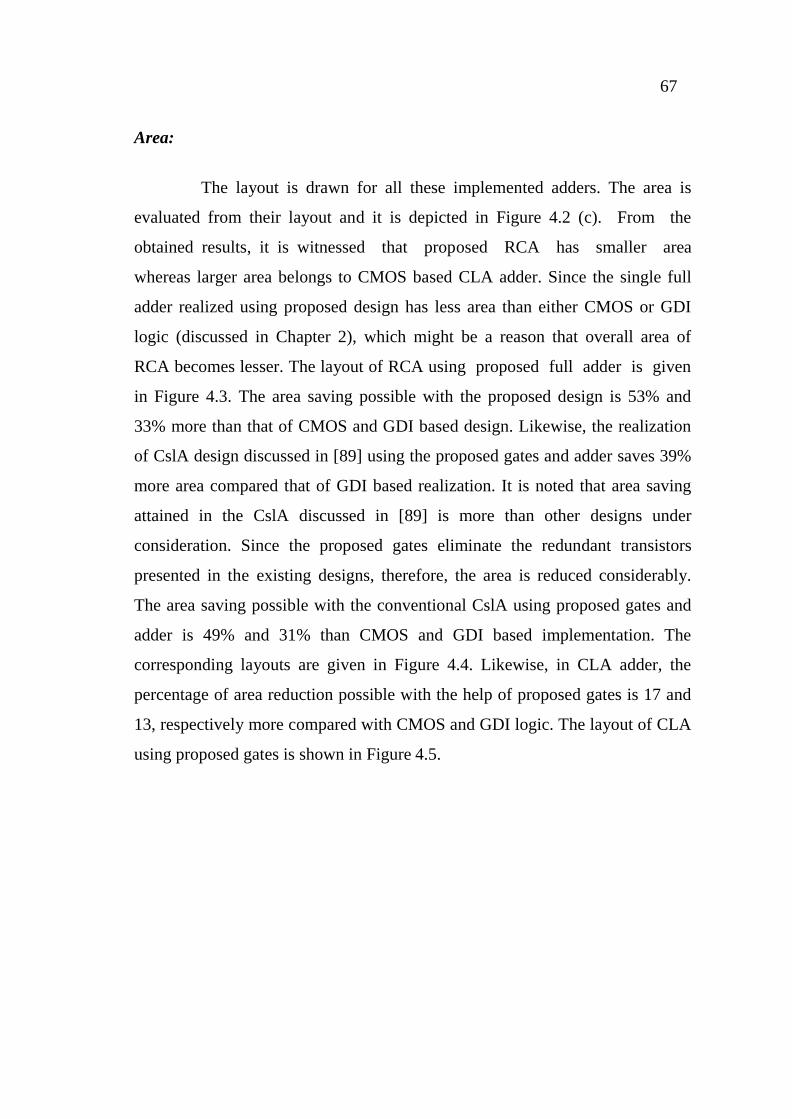
67
Area:
The layout is drawn for all these implemented adders. The area is
evaluated from their layout and it is depicted in Figure 4.2 (c). From the
obtained results, it is witnessed that proposed RCA has smaller area
whereas larger area belongs to CMOS based CLA adder. Since the single full
adder realized using proposed design has less area than either CMOS or GDI
logic (discussed in Chapter 2), which might be a reason that overall area of
RCA becomes lesser. The layout of RCA using proposed full adder is given
in Figure 4.3. The area saving possible with the proposed design is 53% and
33% more than that of CMOS and GDI based design. Likewise, the realization
of CslA design discussed in [89] using the proposed gates and adder saves 39%
more area compared that of GDI based realization. It is noted that area saving
attained in the CslA discussed in [89] is more than other designs under
consideration. Since the proposed gates eliminate the redundant transistors
presented in the existing designs, therefore, the area is reduced considerably.
The area saving possible with the conventional CslA using proposed gates and
adder is 49% and 31% than CMOS and GDI based implementation. The
corresponding layouts are given in Figure 4.4. Likewise, in CLA adder, the
percentage of area reduction possible with the help of proposed gates is 17 and
13, respectively more compared with CMOS and GDI logic. The layout of CLA
using proposed gates is shown in Figure 4.5.

68
Figure 4.3 Layout of 32 bit RCA using proposed adder

69
(a) (b) (c)
Figure 4.4 Proposed gates based 32 bit CslA adder Layout (a)
Conventional (Ref. [172]) (b) BEC based (Ref. [125]) and (c)
Modified (Ref. [89])

70
Figure 4.5 Layout of 32 bit CLA using proposed gates
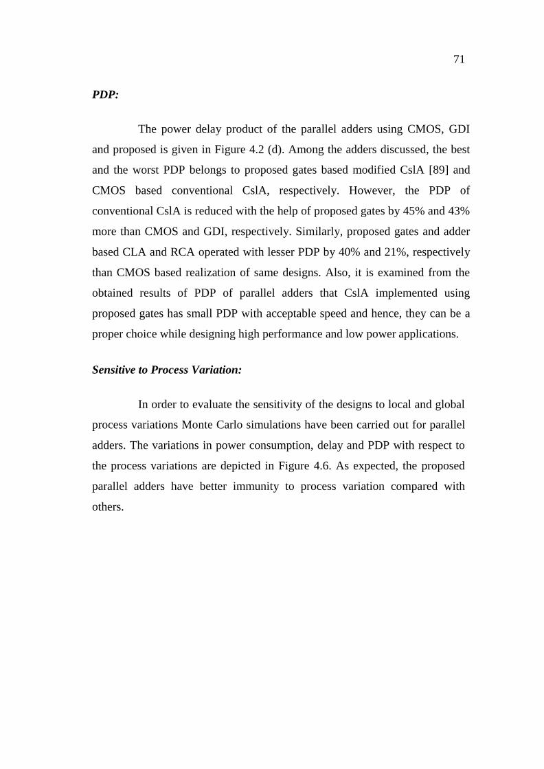
71
PDP:
The power delay product of the parallel adders using CMOS, GDI
and proposed is given in Figure 4.2 (d). Among the adders discussed, the best
and the worst PDP belongs to proposed gates based modified CslA [89] and
CMOS based conventional CslA, respectively. However, the PDP of
conventional CslA is reduced with the help of proposed gates by 45% and 43%
more than CMOS and GDI, respectively. Similarly, proposed gates and adder
based CLA and RCA operated with lesser PDP by 40% and 21%, respectively
than CMOS based realization of same designs. Also, it is examined from the
obtained results of PDP of parallel adders that CslA implemented using
proposed gates has small PDP with acceptable speed and hence, they can be a
proper choice while designing high performance and low power applications.
Sensitive to Process Variation:
In order to evaluate the sensitivity of the designs to local and global
process variations Monte Carlo simulations have been carried out for parallel
adders. The variations in power consumption, delay and PDP with respect to
the process variations are depicted in Figure 4.6. As expected, the proposed
parallel adders have better immunity to process variation compared with
others.
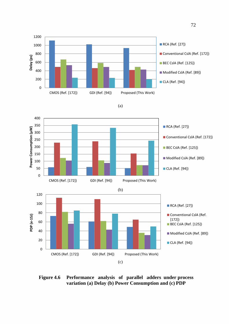
72
Figure 4.6 Performance analysis of parallel adders under process
variation (a) Delay (b) Power Consumption and (c) PDP
(a)
(b)
(c)
0
200
400
600
800
1000
1200
CMOS (Ref. [172]) GDI (Ref. [94]) Proposed (This Work)
De
lay
(ps)
RCA (Ref. [27])
Conventional CslA (Ref. [172])
BEC CslA (Ref. [125])
Modified CslA (Ref. [89])
CLA (Ref. [94])
0
50
100
150
200
250
300
350
400
CMOS (Ref. [172]) GDI (Ref. [94]) Proposed (This Work)
Po
we
r C
on
sum
pti
on
(µ
W) RCA (Ref. [27])
Conventional CslA (Ref. [172])
BEC CslA (Ref. [125])
Modified CslA (Ref. [89])
CLA (Ref. [94])
0
20
40
60
80
100
120
CMOS (Ref. [172]) GDI (Ref. [94]) Proposed (This Work)
PD
P (
e-1
5J)
RCA (Ref. [27])
Conventional CslA (Ref. [172]) BEC CslA (Ref. [125])
Modified CslA (Ref. [89])
CLA (Ref. [94])

73
The performance improvement of parallel adder structures such as
RCA, CslA and CLA with the help of proposed gates and adder is attempted.
It is observed that the proposed gates based RCA and CLA have shown speed
improvement of 12%, and 14%, respectively than CMOS logic. Likewise, the
amount of area reduction achieved in RCA, Modified CslA and CLA based on
proposed gates is 53%, 55% and 28%, respectively more than CMOS logic.
Among the parallel adders, the proposed gates based Modified CslA adder has
shown 43% more improvement in PDP than their existing CMOS
implementation. From the discussion of the performance improvement of
various parallel adders based on proposed gates in GDI logic, CslA adders
have better improvement in PDP than that of RCA and CLA adders.
Therefore, they can be used in the multipliers realization for better
performance.
4.4 SUMMARY
The existing implementation of parallel adders lacks in terms of area
and delay, which is due to the requirement of more transistor count for its
base components such as AND, XOR and adder. To overcome these
drawbacks, proposed gates and adder using GDI logic are employed in the
realization of parallel adders. Further, the performance of the parallel adders
is analyzed using SPICE simulation at 45 nm technology models. The
performance parameters like delay and power consumption of the parallel
adders are measured from their simulation results. In addition, area is
measured from the corresponding layout. From the obtained results, it is
understood that the implemented parallel adders require smaller power delay
product and area compared to the other designs found in the literature.

74
CHAPTER 5
AREA AND ENERGY EFFICIENT VEDIC MULTIPLIER
IMPLEMENTATION
5.1 INTRODUCTION
Designing multiplier with high speed low power and minimal layout
structure is of prime importance. This thesis presents a high speed digital
multiplier by taking the advantage of Vedic multiplication algorithm with low
power design technique called GDI logic. Vedic mathematics is an ancient
Indian mathematics, which was derived from Vedic sutras. It was
rediscovered in the early twentieth century by Maharaja (2001). UT is one of
the Vedic sutras, which literally means vertically and crosswise and is used to
perform a multiplication. In this multiplication process, the partial products
are accumulated at every step as opposed to the conventional multiplication
schemes. Therefore, the speed of this multiplier can be improved by reducing
its partial product accumulation delay. This is attempted in the proposed 8 bit
multiplier. This multiplier computes the output in two stages. At the first
stage, the additions of n bit partial products are performed using n bit adder.
After each addition process, sum and carry outputs are computed and they
move into second stage. It is noted that carry free addition is performed in this
stage. Also, the output bits including sum and carry from the first stage are
not exceeding more than five bits. Therefore, it could be processed efficiently
using 42C rather than with the full adder, which is used in the existing
scheme.

75
A number of interesting methods for realizing a UT multiplier has
been introduced in the last several decades. Several field programmable gate
array realizations of Vedic multiplier are discussed in the literature by Karthik
et al (2012) and Zulhemi et al (2013). They claimed that this multiplier
minimizes the area and improves the speed compared with conventional
multipliers. Also, the multiplier performance improvement in respect of
power, delay and area is attempted by various researchers too. Pushpangadan
et al (2009) introduced a way of developing higher order multiplier from a
smaller one using Vedic multiplication. This was followed by Saha et al
(2011) who implemented 32x32 Vedic multiplier and compared its
performance with Booth radix-4 multiplier. Tiwari et al (2008) discussed the
delay reduction in Vedic multiplier with the help of carry look ahead adder.
This multiplier result indicates that the delay and area of Vedic multiplier is
smaller than array and Booth multiplier.
An introduction of pipeline technique to increase the speed was
discussed by Kunchigi et al (2012). The Vedic multipliers designed with
Random Only Memory (ROM) based approach explained by Sriraman et al
(2012) which offers a significant improvement in speed and power dissipation
compared with conventional multipliers. However, this performance depends
on the reading process of ROM and the subtraction operation. Moreover, the
required area is becoming large for more than 8 bit multiplier. Deepa et al
(2013) had improved multiplier speed by folding and retiming mechanism at
the expense of more area. Vedic multipliers based on carry skip adder
proposed by Senapati et al (2012) offers significant improvement in speed
compared with standard multiplier architectures. The power consumption of
the Vedic multipliers is minimized by implementing them in reversible
(Chanda et al (2013)) and adiabatic logic (Gupta et al (2012)) at the expense
of increase in latency.

76
The Vedic multipliers presented in the existing literature need
further improvement in terms of area, power and speed. This is addressed in
the proposed multiplier. This multiplier delay is reduced with the help of
deployment of 42C in the partial product addition. Also, the GDI logic based
multiplier realization minimizes the power consumption and area. As a whole,
the proposed multiplier has improved the overall performance. The rest of the
Chapter is organized as follows: An overview of the UT multiplication is
briefly given in Section 2. The proposed multiplier is explained in Section 3.
In Section 4, results and discussion are given and the Section 5 concludes the
Chapter.
5.2 AN OVERVIEW OF URDHVA TRIYAGBHYAM
MULTIPLICATION SCHEME
Urdhva Triyagbhyam (UT) is one of the Vedic sutras, which
literally means vertically and crosswise and is used to perform the
multiplication operation. This method requires AND gate, half adder and full
adder for carrying out multiplication operation. It is noted that the partial
products are generated in parallel and become available, prior to actual
addition, thus saving processing time. It is well suited for the multiplication of
both decimal and binary numbers. The mathematical background of UT
algorithm for decimal and binary number multiplication is given below:
5.2.1 UT Algorithm for Decimal Number System
Let X and Y are two numbers to be multiplied. Mathematically X and
Y can be represented as
(5.1)
(5.2)

77
(5.3)
(5.4)
Where X and Y are from 0, 1, 2…, 9 and k may be any integer number.
In the case of 2*2 multiplications, the two inputs are A and B, each
having two digits of X0, X1 and Y0, Y1, providing four outputs P3P2P1P0, as a
result of vertical / crosswise multiplication and addition. The sequential steps
involved in the multiplication procedure are explained as follows:
Step 1: Multiplication process starts from lower digit i.e. X0, Y0 and moves
towards the higher digits X1, Y1.
Step 2: First digit of the product i.e. P0 is obtained by vertical multiplication
of X0 and Y0.
Step 3: For computing P1, do cross wise multiplication of X1, Y0 with X0, Y1,
to get the partial products. After that, perform the addition of these
products, sum is retained as P1. During the addition, if any carry
exists, it is moved to subsequent stage.
Step 4: P2 is obtained from the vertical product of X1 and Y1, provided that
there is no carry from step 3. Otherwise, P2 is obtained after the
addition of vertical product with carry. During this addition process,
any carry occurs, that acts as P3.
As an example, the multiplication of 23 and 22 based on UT method
is illustrated in line diagram as given in Figure 5.1.
The multiplier inputs 23 and 22 are taken as X and Y, having digit X1
X0 as 2 and 3, Y1 Y0 as 2 and 2 respectively.

78
Figure 5.1 Multiplication of 2x2 decimal number using UT algorithm
The concatenation of individual product digit P2P1P0 constitutes the
final product P. Thus, the product is 506.
5.2.2 UT Algorithm for Binary Number System
The UT technique can also be extended to binary number system
and it is found to work accurately. The partial products bits are generated in
single step which minimize the delay associated with the multiplier. For
understanding the multiplication operation, consider the multiplicand and
multiplier represented as X and Y having N number of bits. These two inputs
can be described in mathematical form as

79
(5.4)
(5.5)
xi and yj represent binary numbers may have values of either 0 or 1. The product
of two N bit can be expressed as P where
(5.6)
The multiplication procedure explained for decimal number system
is also holding good for binary number system too.
The advantage of this technique is that all the individual products
are computed in parallel. It increases the speed of operation. But the delay
increases with the increase in number of input bits. This would be a limitation
for this procedure. Hence, this method is suitable for small range of input
though it is appropriate for all cases of multiplication. To mitigate this issue,
multiplier is proposed, without increasing wiring complexity or hardware, by
accounting compressor tree for performing the addition of more than 3 bits at
a time. The various compressors are available in the literature among them
42C is considered for the above said multiplier as it is simple and has regular
interconnection pattern. The discussion of the proposed multiplier and its
implementation is explained in the following Section.

80
5.3 PROPOSED MULTIPLIER
The block diagram of the proposed Vedic multiplier is depicted in
Figure 5.2. The multiplier and multiplicand inputs are represented as X and Y
respectively, and the output is represented as P. The products of Xi.Yj are the
multiplier partial products where the range of i and j is 0 to n-1, n is the
multiplier width. The multiplier partial products are generated from n2
number
of AND gates for n bit input operand. The multiplier output is generated from
these partial products in two stages. In the first stage, these partial products
are added with the help of full adders. Moreover, the parallel addition of
partial products eliminates carry propagation in this stage. This is the
advantage of proposed multiplication technique, whereas in the conventional
scheme carry propagation is allowed, which slows down the multiplication
task. This is illustrated in Figure 5.2, by assigning the individual blocks for
sum and carry outputs to indicate that they are computed in parallel. These
sum and carry outputs are becoming inputs for the second stage computation.
Partial products generation
using AND gates
Adder
Sum outputs Carry outputs
Adder and 4-2 Compressor
Final product bit
(P2n-1,…,P1)
First stage
Second stage
Multiplicand (X) Multiplier (Y)
nn
P0(X0.Y0)
Figure 5.2 Block diagram representation of the proposed Vedic multiplier

81
Figure 5.3 Internal architecture of the proposed Vedic multiplier (a)
First stage and (b) Second stage
2 BIT
ADDERx1y0
x0y1
P1
C1
3 BIT
ADDER
x2y0
x0y2
S2C2
x1y1
4 BIT
ADDER
x3y0
x0y3
S3C3
x2y1x1y2
C4
5 BIT
ADDER
x4y0
x0y4
S4
C5x3y1x1y3 C6x2y2
6 BIT
ADDER
x5y0
x0y5
S5
C7x4y1x1y4 C8x3y2x2y3
7 BIT
ADDER
x6y0
x0y6
S6
C9x5y1x1y5
C10x4y2x2y4x3y3
8 BIT
ADDER
x7y0
x0y7
S7
C11x6y1x1y6 C12x5y2x2y5x4y3x3y4
C13
7 BIT
ADDER
x7y1
x1y7S8
C14x6y2x2y6
C15x5y3x3y5x4y4
6 BIT
ADDER
x7y2
x2y7
S9
C16x6y3x3y6
C17x5y4x4y5
5 BIT
ADDER
x7y3
x3y7
S10
C18x6y4x4y6 C19x5y5
4 BIT
ADDER
x7y4
x4y7
S11
C20x6y5x5y6
C21
3 BIT
ADDER
x7y5
x5y7
S12
C22x6y6
2 BIT
ADDER
x7y6
x6y7
S13
C23
2 BIT
ADDERP2
S2
C1
3 BIT
ADDER P3
S3
C2
3 BIT
ADDER
S4
C3P4
4-2 C P5S5
C4
C5
4-2 C P6S6
C6
C7
4-2 C
P7S7
C8
C9
C5B
C5B
C7B
C9B
4-2 C
P8S8
C10
C11
C7B
C11B
4-2 C P9
S9
C12
C14
C9BC13B
4-2 C
P10S10
C13
C15
C16
C15B
4-2 C
P11S11
C17
C18
C13B
C17B
4-2 C P12
S12
C19
C20
C15BC19B
4-2 C P13
S13
C21
C22
C17B
C21B
4-2 C P14
S14
C23
C19B C23B
3 BIT
ADDER
C23B
C21BP15
(a) (b)

82
The inputs of the first stage are from the partial products which are
generated based on Vedic multiplication, after that, they are accumulated
directly using n bit adder for n bit partial products and their sum and carry
outputs are represented as S and C, respectively. They act as the inputs for the
second stage. This comprises of adder and 42C to perform the addition task.
The arrangement of 42C in the final addition process will increase the
multiplier speed. In the second stage, full adder and 42C are deployed from
which final multiplier output is obtained. The full adder and 42C are used in
the place of addition of three and more than three bits, respectively. It is
interesting that the use of full adder for the addition of more than three bits is
eliminated with the help of 42C. Due to the use of 42C, carry free addition is
performed in the second stage increasing the multiplier speed. Not only that,
the regular interconnection pattern of compressor also minimizes the
multiplier interconnection complexity. The internal architecture details of the
first and second stage of the proposed multiplier are given in Figures 5.3(a)
and 5.3 (b), respectively. The notation of 4-2 C in the Figure 5.3(b) represents
42C.
5.4 RESULTS AND DISCUSSION
In this Section, the simulation results of both the proposed and the
existing multiplier are presented. The performance parameters such as area,
delay, power consumption and PDP of multiplier are evaluated through the
SPICE simulation results at 45 nm technology with a supply voltage (VDD) of
1.1 V. The simulation results of multiplier in respect of delay, power
consumption and layout area are given in Table 5.1. After the completion of
simulation of multipliers, the layout is generated for each of them and
subjected to DRC and then LVS check before the extraction of parasitic.
Subsequently, the extracted parasitic file is back annotated to perform the post
layout simulation.

83
Table 5.1 Performance comparison of 8 bit proposed multiplier with
existing designs
S. No. Multiplier Delay
(ps)
Power Consumption
(µW)
Area
(µm2)
PDP
(e-15 J)
1 Ref. [118] 552 83 2415 45.8
2 Ref. [74] 465 78 1678 36.2
3 Proposed
(This Work)
432 68 1164 29.3
Delay:
The delay is calculated from the 50% of the voltage level of the
input to 50% voltage level of the resulting output voltage for each transition.
The maximum delay is taken as worst case delay. In the proposed multiplier
carry propagation is eliminated during the partial products addition thus
reducing the delay significantly. The speed improvement obtained by the
proposed multiplier is 22% more than the multiplier discussed in [118].
Power Consumption:
The power consumed by the multipliers is computed through
simulation and given in Table 5.1. It is observed from the results that the
proposed multiplier design has lesser power consumption than that of existing
designs. This is due to the implementation of its building components namely,
AND gate, full adder and 42C using proposed design, which minimizes the
multiplier transistor count considerably and spurious transitions, thus reducing
the overall power consumption. The power saving accomplished in the
proposed design is 13% more compared to the Vedic multiplier discussed in
[74]. Also, it is noted that the use of multichannel technique minimizes the
power consumption compared to the multiplier discussed in [118]. However,
the variation of threshold voltage, necessitated by the multichannel process, is
becoming a difficult task during the fabrication process.
84
Area:
The layouts are drawn for all the simulated multiplier and the area is
calculated from them. The values are given in Table 5.1. From the obtained
results, it is observed that the proposed multiplier has 31% lesser area
compared to the recently reported Vedic multiplier in [74]. The layout of the
proposed Vedic multiplier is given in Figure 5.4.
PDP:
The power delay product of the proposed and existing multiplier
designs is given in Table 5.1. The power consumption is minimized
considerably by implementing the proposed multiplier using GDI logic. Also,
the delay is reduced in the proposed multiplier. Hence, the energy (or power
delay product) saving accomplished with proposed design is 36% more than
the multiplier discussed in [118].

85
Figure 5.4 Layout of the proposed Vedic multiplier

86
Sensitive to Process Variation:
A study of circuits performance under the local and global process
variations is carried through Monte Carlo simulations and the results are
tabulated in Table 5.2. It is observed that the proposed multiplier has better
immunity to process variation. Moreover, the design based on multichannel
technique, discussed in [74] is more sensitive because of driving current
dependency on the process sensitivity Vt, which is amplified due to voltage
drops at internal nodes.
Table 5.2 Performance analysis of multipliers under process variation
S. No. Multiplier Delay
(ps)
Power Consumption
(µW)
PDP
(e-15 J)
1 Ref. [118] 569 87.2 49.6
2 Ref. [74] 484 81.5 39.4
3 Proposed
(This Work)
441 69.2 30.5
5.5 SUMMARY
This thesis presents an approach to design Vedic multiplier, in such
a way to improve its speed with the help of deploying 42C in its architecture,
without increasing area. Due to the presence of 42C in this multiplier
architecture, the number of full adders is reduced compared to the existing
design. Though the existing and proposed Vedic multipliers have same
number of stages to perform in the multiplication operation, the delay of
proposed multiplier is reduced by generating intermediate carries which is
independent of carry in inputs. Also, the basic components of multiplier such
as AND gate, adder and 42C have been implemented using proposed designs.
The proposed and the existing multiplier designs are simulated using 45 nm

87
technology model. The comparison is done in terms of delay, power
consumption, area and PDP. The proposed design has shown 35% more
improvement in power delay product compared with the existing multiplier
reported in the literature. The effect of process variation on the multipliers
performance has been analysed through Monte Carlo simulations. From the
obtained results, it is concluded that the proposed multiplier has shown about 2%
performance variations. Hence, this fast energy efficient multiplier can be used as
one of the building modules for the realization of real time signal processing
applications.

88
CHAPTER 6
HIERARCHY MULTIPLIER ARCHITECTURE BASED ON
VEDIC MATHEMATICS AND GDI LOGIC
6.1 INTRODUCTION
Hierarchy multiplier is attractive because of its ability to carry the
multiplication operation within one clock cycle. The existing hierarchical
multipliers occupy more area and also results in more delay. Therefore, in this
Chapter 6, a method to reduce the computation delay of hierarchy multiplier
by employing CslA and BEC is proposed. The use of BEC eliminates the
number of adders, existing in the conventional addition scheme, where n
denotes the multiplier input width. As the area of the hierarchy multiplier is
determined by its base multiplier, the base multiplier is realized with the
proposed Vedic multiplier, which has small area and operates with less delay
than the conventional multipliers. In addition, the reduction of power
consumption in the hierarchy multiplier can be ensured by implementing the
designed multiplier using GDI logic.
In general to design n bit hierarchical multiplier, four
2 base
multipliers are necessary which generate 2n bit output, where n represents
hierarchical multiplier input width. It is noted, all the base multipliers are
allowed to perform the task in parallel. Due to that, the performance of the
hierarchy multiplier is determined from the accumulation delay of its base
multipliers output bits. But this is a time consuming task as it requires more
number of additions and is considered as a bottleneck for the hierarchy

89
multiplier performance. In this work, an approach to perform this
accumulation with less number of addition process is proposed. The following
are the contributions discussed in the Chapter:
(i) For the area and delay efficient implementation of base
multiplier, Vedic multiplier( discussed in previous Chapter) is
considered
(ii) To reduce the accumulation delay of base multiplier output
bits, CslA and BEC are introduced
(iii) To realize the hierarchy multiplier with small area, GDI logic
is chosen
The rest of the Chapter is organized as follows: An overview of the
hierarchy multiplier is described in Section 2. In Section 3, the explanation of
the proposed hierarchy multiplier and the implementation of its building
components namely, base multiplier, CslA adder, BEC converter are also
given. The simulation results and discussion are given in Section 4 and finally,
the Section 5 summarizes the Chapter.
6.2 AN OVERVIEW OF HIERACHY MULTIPLIER
Hierarchy multiplier is significant because of its ability to carry
multiply operation within one clock cycle. The major concern in designing
such multiplier is to minimize the overhead in terms of circuit footprint,
power consumption and computational delay that is required to achieve
reconfigurable. The basic hierarchical topology of large width multiplication
is given in Figure 6.1. After hierarchically decomposed, this scheme needs a
set of base multipliers. For this, the high performance and resource efficiency
of the built in hardware multipliers based on Vedic mathematics is considered
in the proposed hierarchy multiplier design.

90
Given two n*n n unsigned binary numbers X and Y, conventional
principle for calculating X *Y with
2 *
2 multipliers can be expressed as
P = X * Y = (XH.XL) * (YH.YL ) (6.1)
where XH, XL and YH.YL represent the lower and higher order input bits of X
and Y. Eq.(6.1) suggests that a n * n multiplication can be carried in two steps
as depicted in Figure 6.1.
Figure 6.1 Representation of hierarchy multiplier
First, 4n partial products are produced from four n * n multipliers
i.e. executing four n*n multiplications in parallel. Second, the partial products
are summed by using one stage carry save array adder and a fast carry
propagate adder to obtain final 4n bit product. In this way large width
multiplier is implemented with the help of smaller modules. Note that four
multiplier outputs are computed in parallel. In order to perform this, four
2 bit
multipliers are required. It achieves high computation performance by
exploiting parallelism in computing the partial products. The hierarchical
XHYH XH YL XLYH XLYL
Carry Save Adder
Carry Select Adder
XH XL YH YL
Pn-1-0P2n-1:n
X Y

91
principle helps to realize fast large bit multiplier, except that it requires a large
adder for performing the addition process. This large adder poses limitation
on the performance and increases the area of designed multiplier.
The above mentioned issues in the existing hierarchy multiplier can
be addressed by
(i) Incorporating BEC to eliminate n/4 number of adders at the
final stage of addition process
(ii) Performing the final addition using CslA
(iii) Implementing the proposed hierarchy multiplier using GDI
logic
6.3 METHODOLOGY
In this Section, an approach for efficient implementation of n bit
hierarchy multiplier with minimum delay will be presented and discussed. As
an example, the architecture for 16 bit multiplier design is explained. Further,
a new design is suggested for the hierarchy multiplier building block namely,
base multiplier based on Vedic mathematics. Following that, the discussion of
CslA, binary to excess 1 converter and GDI logic is carried out in this Section.
6.3.1 Proposed Hierarchy Multiplier
In general, the hierarchy multiplier speed is determined from the
computation delay of base multiplier output bits addition. This delay can be
decreased by minimizing the number of additions without affecting the
functionality. The following approach is incorporated in the proposed n bit
hierarchy multiplier multiplication procedure to reduce the delay:
92
Step 1: The multiplier inputs and output are represented as X, Y and Z,
respectively.
Step 2: Divide n bit multiplier inputs i.e., X and Y, into equal two halves.
For the input X, it is divided into (Xn,… Xn/2), (Xn/2-1,…, X0), which
are assigned as XH and XL, respectively. The same procedure is also
adopted for another multiplier input Y.
Step 3: After dividing both the inputs, they are formed into four groups like
(XL, YL), (XH ,YL), (XL ,YH) and (XH, YH).
Step 4: The multiplication is accomplished using four
2 bit base multipliers
namely, a0, a1, a2 and a3.
Step 5: The multiplier product bits Zn/4-1,…, Z0 is obtained from 0 to
2-1
output bits of a0.
Step 6: The resultant bits of a1, a2 and concatenation of a0 (
2 to n), a3 (0 to
2-
1) will be formed an array of carry save format which are processed
by carry save adder.
Step 7: The resultant sum and carry from carry save adder are becoming the
inputs for CslA of n bit adder. Also, the sum output of CslA adder is
assigned as multiplier resultant bits for the range of Zn+n/2-1,…, Zn/2.
Step 8: BEC takes the input from a3 (
2 to n bit) and its output bits are
available prior to CslA and they are passed to a multiplexer.
Step 9: The multiplier output bits Z2n,…, Zn+n/2 is obtained from the
multiplexer, based on the carry output of CslA adder, if it is one
then the BEC output becomes the output otherwise the product bits
of a3 (
2 to n bit).

93
Based on this approach, 16 bit (n) hierarchy multiplier architecture
is designed as shown in Figure 6.2. The multiplier inputs are X, Y of 16 bit
width and produces the output Z of 32 bit. First, the inputs X and Y are divided
into equal two halves namely, XH and XL, YH and YL and they are multiplied by
8 bit base multiplier. As seen in Figure 6.2, the symbols of a0, a1, a2 and a3
denote the base multiplier for the multiplication of (XL and YL), (XH and YL),
(XL and YH) and (XH and YH), respectively. Once these multiplication processes
are over, their output bits will form a carry save array as per step 6, which in
turn is processed by carry save adder thus resulting into two rows of 16 bit
output. These bits are further added with the help of 16 bit CslA adder to
produce the multiplier output bits of Z23,…, Z8. Meanwhile, the BEC also
computes its output and feeds to multiplexer as one of the inputs. Another
input for the multiplexer is from a3 output (half of the output bits i.e., n/2 to n-
1). Finally, the multiplexer selects, either BEC or a3 output bit as Z24 to Z31,
based on CslA adder’s carry
Figure 6.2 Proposed 16 bit hierarchy multiplier
Multiplier
a2
CSA adder
CslA adderMUX
Multiplier
a1
Multiplier
a0
Multiplier
a3
BEC0 to n/2-1 bits
(M)
n/2 to n-1 bits
(M)
0 to n/2-1 bits (P)
0 to n-1 bits
(N)0 to n-1 bits (O)
sc
s
c
n/2 to n-1 bits
(P)
Z7Z6Z5Z4Z3Z2Z1Z0Z15Z14Z13Z12Z11Z10Z9Z8Z23Z22Z21Z20Z19Z18Z17Z16Z31Z30Z29Z28Z27Z26Z25Z24
XLYLXL YL XHYHYH XH

94
As a result of introduction of BEC in the hierarchy multiplier, n/4
adders are eliminated. Due to the parallel computation of BEC and CslA
output, the processing delay for multiplier output bits i.e., Z24 to Z31 is
minimized significantly. As seen from the architecture of proposed hierarchy
multiplier, given in Figure 6.2, the critical path of the proposed architecture
consists of one base multiplier, one bit adder, one CslA adder and multiplexer
only. Further, the implementation details of building components of the
hierarchy multiplier namely, base multiplier, CslA adder and BEC converter
are described in the following subsection.
6.3.2 Base Multiplier
As discussed in the earlier Section, the performance of the hierarchy
multiplier is determined by its base multiplier. In the conventional
multiplication techniques, the intermediate computation involved in the
multiplier operation reduces the speed exponentially in accordance with the
number of bits present in multiplier input. This becomes critical issue for
more number of input bits. But this issue can be mitigated by the parallel
addition of partial products which is an inherited principle of Vedic
multiplication method. Though partial products reduction is possible in Booth
multiplication, the encoding and decoding mechanism involved in this method
increases the circuit complexity thereby power consumption. On the other
hand, Wallace multiplication uses random placement of counters for the
efficient partial product accumulation thus makes the design becomes
complex than the conventional scheme. Therefore, the Vedic multiplication is
considered as an alternative way of performing the multiplication operation
without increasing the circuit complexity and power consumption. In this
multiplication process, the partial products are accumulated at every step as
opposed to the conventional multiplication schemes. Therefore, the speed of
this multiplier can be improved by reducing its partial product accumulation
delay. This is attempted in the proposed 8 bit multiplier and its representation
is shown in Figure 6.3.

95
The multiplier inputs and outputs are represented as Xi, Yi and P2i,
where i is 0 to n-1, n denotes the input bit width (for 8 bit multiplier, n=8).
The multiplier partial products (X.Y) are generated using AND gates. From
them, the partial product of X0.Y0 is output bit of multiplier, i.e., P0, whereas
the remaining output bits are obtained after two stage computation. In the first
stage, the partial products generated from AND gates which are added using
adder. After each addition process, sum and carry are computed and they
move into second stage. It is noted that carry free addition is performed in this
stage. Also, these output bits including sum and carry from the first stage are
not exceeding more than five bits. Therefore, 42C is chosen for adding of
these bits rather than full adder, which is used in the existing scheme. Due to
the use of 42C, carry free addition is ensured in the second stage too.
Partial products generation
using AND gates
Adder
Sum outputs Carry outputs
Adder and 4-2 Compressor
Final product bit
(P2n-1,…,P1)
First stage
Second stage
Multiplicand (X) Multiplier (Y)
nn
P0(X0.Y0)
Figure 6.3 Block diagrammatic representation of base multiplier

96
6.3.3 Carry Select Adder
There are various adders employed for the addition of base
multiplier product bits. They are namely, ripple carry, carry look ahead, carry
select and prefix adder. It is well known from the performance study of these
adders that CslA has modest performance in terms of area and delay
[Ramkumar and Kittur 2012 and Mohanty and Patel 2014]. Also, proposed
gates based CslA adder has shown improved performance which is
elaborately discussed in (Chapter 5). Therefore, CslA adders are chosen as
parallel adder while implementing the proposed hierarchy multiplier
architecture.
6.3.4 Binary to Excess 1 Converter
To reduce the delay of partial products addition in the hierarchy
multiplier, this work uses BEC instead of adder for the output bits of Z2n-
1,…,Zn+n/2,. For n bit input width, n+1 bit BECs are required. A structure of 4
bit BEC is shown in Figure 6.4.
B3 B2 B1 B0 B0
X3 X2 X1 X0
Figure 6.4 4 bit BEC circuit

97
6.4 RESULTS AND DISCUSSION
In this section, the simulation results of the 16 bit hierarchy
multiplier and 8 bit binary to excess 1 converter are presented. The
performance parameters such as area, delay, power consumption and PDP of
the simulated designs are evaluated through the SPICE simulation at 45 nm
technology with a supply voltage (VDD) of 1.1 V. Typical transistor sizes, i.e.,
(W/L)p=240 nm/45 nm and (W/L)n=120 nm/45 nm are considered. The delay
and power consumption are calculated as follows: The delay is computed by
accounting the time from the 50% of the input voltage swing to 50% of the
output voltage swing for each transition. The maximum delay is treated as
worst case delay. Likewise, the power consumption is determined from the
various switching activities and the capacitances of circuit. These procedures
are extended for the delay and power consumption calculation of all the
simulated modules namely, proposed hierarchy multiplier and binary to
excess 1 converter.
6.4.1 Proposed Hierarchy Multiplier
The simulation results of the proposed and existing multipliers are
given in Table 6.1.
Delay:
The delay computed through simulation, for all the structures, is
given in Table 6.1 and it is observed that the proposed multiplier has smaller
delay compared to other existing implementations. Due to the deployment of
BEC converter in the base multiplier output bits accumulation, the numbers of
adders are reduced, thus decreasing the delay significantly. Moreover, the
time taken for the binary to excess 1 converter is not accounted in the critical
path delay thereby the speed is improved. The speed improvement obtained

98
by the proposed design is 27% and 11% more than that of multiplier
discussed in [70] and [1] , respectively.
Table 6.1 Performance comparison of the proposed 16 bit hierarchy
multiplier with other multipliers
S. No. Multiplier Delay
(ps)
Power Consumption
(µW)
Area
(µm2)
PDP
(e-15 J)
1 Ref. [70] 727 658 14510 478
2 Ref. [16] 657 563 14978 369
3 Ref. [1] 594 608 15210 361
4 Proposed Hierarchy
Multiplier (This Work)
528 424 12420 223
Power Consumption:
The power consumed by the simulated hierarchy multipliers is
presented in Table 6.1. The minimum power consumption is witnessed in the
proposed design due to the elimination of redundant hardware exhibited in the
existing designs thus minimizing the spurious activities. The proposed design
has 30% less power consumption than that of multiplier discussed in [1].
Area:
The area is computed from the layout of simulated multipliers and it
is given in Table 6.1 whereas the layout of the proposed multiplier is given in
Figure 6.5. From the obtained results, it is witnessed that proposed multiplier
has less area. As stated earlier, the proposed gates and adder are used to
implement the basic components of hierarchical multiplier namely, base
multiplier, CslA adder, BEC converter with reduced transistor count.
Therefore, the area of the proposed hierarchical multiplier is small. The
percentage of area reduction possible with proposed design is about 18%
more than that of a recently reported multiplier in [1].

99
PDP:
The power delay product of the all simulated designs is given in
Table 6.1. Among the multipliers discussed, the best and the worst PDP
witnessed correspond to the proposed and the design discussed in [70],
respectively. Also, the energy conservation accomplished with proposed
design is 38% more than the multiplier reported in [1].
Figure 6.5 Layout of the proposed 16 bit hierarchy multiplier

100
Sensitive to Process Variation:
The sensitivity of the circuit’s performances namely, delay and
power consumption under process variations are studied through Monte Carlo
simulations and their results are given in Table 6.2. The performance
variations are noted as 3%, which is lesser than the existing hierarchy
multiplier results.
Table 6.2 Performance analysis of 16 bit hierarchy multiplier under
process variation
S. No. Multiplier Delay
(ps)
Power Consumption
(µW)
PDP
(e-15 J)
1 Ref. [70] 769 698 536
2 Ref. [16] 692 607 420
3 Ref. [1] 634 638 404
4 Proposed Hierarchy
Multiplier (This Work)
541 441 238
6.4.2 Binary to Excess 1 Converter
The gates of BEC are designed based on CMOS, CPL, GDI and
proposed one. The performance parameters in respect of delay and power
consumption are calculated from the simulation results and tabulated in Table
6.3. As seen from the values the realization of BEC, using proposed gates,
improves its performance compared with the CMOS and CPL.

101
Table 6.3 Performance comparison of 8 bit BEC
S. No. Design Delay
(ps)
Power Consumption
(µW)
Area
(µm2
)
PDP
(e-18 J)
1 Ref. [172] 203 15 537 3045
2 Ref. [45] 188 21 583 3948
3 Ref. [94] 245 11 501 2695
4 Proposed
(This Work)
173 9 445 1557
The delay and power consumption of the BEC, based on proposed
gates, is reduced by 15% and 40%, respectively compared to conventional
CMOS realization. The area is calculated from their layout and is given in
Table 6.3. It is observed that the 17% more area saving is possible with
proposed BEC design than CMOS based implementation. The layout of
proposed BEC is shown in Figure 6.6. Further, Monte Carlo simulation is also
performed to study the circuit robustness under process variation. From the
results, it is noted that proposed BEC circuit has shown 1% performance
variation with respect to process changes.

102
Figure 6.6 Layout of the proposed 8 bit BEC
6.5 SUMMARY
A BEC converter based hierarchy multiplier architecture is proposed
here. It operates with shorter delay due to the removal of n/4 number of
adders, presented in the existing hierarchy multiplier. Moreover, the delay
incurred by BEC is not affecting the hierarchical multiplier because it is not
included in the critical path of the multiplier. In addition to that, a new design
for base multiplier is proposed, based on Vedic mathematics. It has less delay
and small area compared to other multipliers found in the literature. The
major outcome of the proposed design is that the number of adders has been
reduced is more while other reported works remain high. Also, the realization
of proposed multiplier using proposed gates and adder reduces its power
consumption and area. Thus, area-power and delay efficient hierarchy
multiplier is designed. The performances of delay and power consumption of

103
the existing and the proposed hierarchy multipliers are calculated through SPICE
simulation using 45 nm technology model. From the simulation results, it is
calculated that the energy saving achieved by the proposed multiplier design is
38% more than the recently reported multiplier. Further, the multipliers
performance study with respect to process variations is done and examined that
the proposed multiplier has shown 3% performance variation, which is less than
their counterparts. Therefore, the proposed multiplier can be used in the media
processing applications in which large width multiplier with less energy
consumption is of prime importance.

104
CHAPTER 7
CONCLUSION AND FUTURE WORK
7.1 CONCLUSION
This dissertation is mainly focused on the design of arithmetic
circuits namely, full adder, 4-2 compressor, parallel adders and multiplier
with the help of full swing gates in GDI logic. The low power high speed
multiplier with small area is possible by adopting Vedic mathematics based
multiplication technique followed by transistor level implementation carried
out using GDI logic. The merits of GDI logic are to implement the basic
modules of multiplier namely, AND gate, adder and 4-2 compressor with low
power consumption and less transistor count. A new method for partial
products accumulation in the Vedic multiplication has been discussed and
further implemented using GDI logic. Moreover, the scalability of the
designed multiplier is also analyzed through hierarchy multiplication
principle. In addition, the performance of all the designed circuits with respect
to process variation are studied through Monte Carlo simulation and it is
observed that proposed designs show lesser performance parameter changes
than their counterparts. The novelty and significance of these mechanisms are
listed below:
From the operational characteristics of GDI gates, it is concluded
that they produce reduced output voltage, i.e. the output high (or low) voltage
is deviated from the VDD (or GND) by threshold voltage Vt for certain input
combinations. The placement and proper biasing of PMOS or NMOS

105
transistor at the output terminal, depending on the voltage deviation either from
VDD or GND potential, provides full swing output. Based on this technique AND,
OR, XOR and XNOR are designed. From the simulation results of the gates, it is
understood that the proposed gates using GDI logic have shown improved
performance compared to that of conventional GDI designs. The proposed AND,
OR, XOR and XNOR gates operated with less delay by 5%, 45%, 66% and 62%,
respectively than existing gates based on GDI. Likewise, the power conservation
in proposed AND, OR, XOR and XNOR gates are 10%, 12%, 30% and 27%,
respectively more than those available GDI gates. The area reduction attained in
the AND, OR, XOR and XNOR gates are 24%, 23%, 24% and 17%, respectively
more than existing GDI based on those designs. Further, the performance
variations of these proposed gates with respect to process changes are calculated
from Monte Carlo simulation and 1% variation is observed.
With the help of the proposed gates, three designs for full adder are
designed. It is observed from the computed delay values, among the three
proposed designs, Design 2 has the lowest delay since Cout and Sum are
computed in parallel. The full adder design based on Design 2 operates faster
by 41% more than CMOS full adder. Also, the power consumption results
reveal that the three proposed adders consume low power. Among the
proposed adders, Design 1 consumes low power since it adopts the proposed
XOR gate and requires minimum transistor count than the other two proposed
design. The percentage of power savings attained with Design 1 than
conventional GDI adder is 30. Not only power and delay, it is observed that
three proposed full adders consume small amount of energy. This is due to the
presence of full swing gates in the proposed full adders. These full swing
gates will only switch the required transistor for the particular input. In
addition to that, all three designs require less transistor count that results into
reduction of the gate capacitance. Hence, they consume less energy. The

106
amount of energy saving can be possible with Design 2 is 32% more than
CMOS. It can be concluded that proposed adder Design 2 is having higher
immunity to process variation in both delay and power distribution.
A new design for 4-2 compressor is proposed based on
simplification of its Boolean output expression. Due to the simple and regular
architecture the power consumption of the proposed 4-2 compressor is less.
Moreover, this design is implemented using proposed gates in GDI logic thus
results in small area. The percentage of area reduction is possible with
proposed 42C which is about 9% more than that of a recently reported
compressor. Moreover, the energy saving accomplished with proposed design
is 41% more than the existing compressor. The sensitivity of the designed
compressor under global and local variations is computed from Monte Carlo
simulation and the results reveal that the performance deviation of the
proposed compressor is about 1%.
The parallel adders performance are improved with the help of
proposed gates and adder using GDI logic. Simulation results reveal that the
delay and PDP of RCA is reduced by 12% and 16%, respectively more than
CMOS based design. Likewise, modified CslA design implemented using
proposed gates possesses decreased delay and power consumption by 14%
and 15% more compared that of GDI based existing implementation.
Similarly, the proposed gates based CLA improves the speed by 44% more
and decreased the power consumption by 19% less. Along with these
attributes, the reduction in energy consumption is achieved in proposed gates
based RCA, Modified CslA and CLA is 16%, 43% and 40%, respectively
more than CMOS based implementation. In addition, the functionality of the
implemented adders under process changes is studied from Monte Carlo
simulation and observed that they possess less variation about 2%.

107
A new architecture for performing multiplication with less
computational delay using Vedic mathematics is proposed. This multiplier
uses 4-2 compressors in the place of adders which are used in the existing
scheme. The speed improvement obtained by the proposed multiplier is 22%
more than the conventional multiplier. The proposed multiplier design has
lesser power consumption which is achieved due to the implementation of its
building components namely, AND gate, full adder and 4-2 compressor using
proposed designs, which minimizes the requirement of transistor count
considerably, thereby spurious transitions, thus reduces the overall power
consumption. Also, the energy saving accomplished with proposed design is
35% more than the conventional multiplier. The proposed multiplier has 31%
lesser area compared with the recently reported Vedic multiplier. A study of
circuits performance under the local and global process variations is carried
through Monte Carlo simulations and the results are validate that the proposed
multiplier possess 2% performance variation.
The hierarchy multiplier architecture is modified by incorporating
BEC in the place of adder to reduce the processing delay. The speed
improvement obtained by the proposed design is 27% more than that of the
existing multiplier. Also, minimum power consumption is witnessed in the
proposed design due to the elimination of redundant hardware exhibited in the
existing designs thus minimizes the spurious activities. The proposed design
has 30% less power consumption than that of existing multiplier. Also, the
energy conservation accomplished with proposed design is 38% more than the
existing hierarchy multiplier. The percentage of area reduction possible with
proposed design is about 18% more than that of a recently reported hierarchy
multiplier. The sensitivity of the circuit’s performances namely, delay and
power consumption under process variations are studied through Monte Carlo
simulations. It is examined that the proposed hierarchy multiplier has 3%
performance variation.

108
7.2 SCOPE FOR FUTURE WORK
There are many directions to extend the experiments presented in
this thesis. The following is a brief list of suggestions for possible future work
in this research domain.
The performance of multiplier can be investigated under
signal processing applications such as filtering,
transformation and so on
The implementation of squaring and cubic operations using
Vedic mathematics can be done

109
REFERENCES
1. Abbasi S A, Zulhelmi A R M and Alamoud A (201 , “FPGA design,
simulation and protyping of 32 bit pipeline multiplier based on Vedic
mathematics”, IEICE Electronics Express, vol. 12, no. 1 , Jul.,
pp. 1-12.
2. Abdoreza Pishvaie, Ghassem Jaberipur and Ali Jahanian (2014),
“High-performance CMOS (4:2 compressors”, International Journal
of Electronics, vol. 101, no. 11, Jan., pp.1511–1525.
3. Abdoreza Pishvaie, Ghassem Jaberipur, Ali Jahanian (2012),
“Improved CMOS (4;2 compressor designs for parallel multipliers”,
Computers & Electrical Engineering, vol. 38, no. 6, Nov., pp. 1703-1716.
4. Abhilash R, Raju I B K, Chary G and Dubey S (201 , “Area-power
efficient Vedic multiplier using compressors”, In Proc. of International
Conference on Electrical, Electronics, Signals, Communication and
Optimization, pp. 1-5.
5. Abiri E, Salehi M R and Darabi A (2014 , “Design and simulation of
low-power and high speed T-Flip Flap with the modified gate diffusion
input technique in nano process”, In Proc. of Iranian Conference on
Electrical Engineering, pp. 82-87.
6. Akhter S (200 , “VHDL implementation of fast NxN multiplier based
on Vedic mathematics”, In Proc. of European Conference on Circuit
Theory and Design, pp. 472-475.
7. Akhter S, Chaturvedi S and Pardhasardi K (201 , “CMOS
implementation of efficient 16-Bit square root carry-select adder”,
International Conference on Signal Processing and Integrated
Networks, pp. 891-896.

110
8. Amrutur B and Horowitz M (2001 , “Fast low-power decoders for
RAMs”, IEEE Journal of Solid-State Circuits, vol. 36, no. 10, Oct.,
pp. 1506–1515.
9. Amuthavalli G and Gunasundari R (201 , “Analysis and design of
subthreshold leakage power-aware ripple carry adder at circuit-level
using 0nm technology”, In Proc. of Procedia Computer Science,
vol. 48, pp. 660-665
10. Anders M, Mathew S, Bloechel, B, Thompson S, Krishnamurthy R,
Soumyanath K and Borkar S (2002 , “A . GHz 1 0 nm single-ended
dynamic ALU and instruction-scheduler loop”, In Proc. of IEEE
International Solid States Circuits Conference, pp. 410–411.
11. Anitha R, Deshmukh N, Agarwal P, Sahoo S K, Karthikeyan S P and
Reglend I J (201 , “A 2 bit MAC unit design using Vedic multiplier
and reversible logic gate”, In Proc. of International Conference on
Circuit, Power and Computing Technologies, pp. 1-6.
12. Anjana R, Abishna B, Harshitha M S, Abhishek E, Ravichandra V and
Suma M S (2014 , “Implementation of Vedic multiplier using Kogge-
stone adder”, In Proc. of International Conference on Embedded
Systems, pp. 28-31.
13. Anuar N, Takahashi Y and Sekine T (200 , “4-bit Ripple carry adder
using two phase clocked adiabatic static CMOS logic”, In Proc. of
IEEE Region 10 Conference, pp. 1-6.
14. Archana S and Durga G (2014 , “Design of low power and high speed
ripple carry adder”, In Proc. of IEEE International Conference on
Communications and Signal Processing, pp. 939-943.
15. Arun and Kumar M (2014 , “Design of low power split path Data
Driven Dynamic ripple carry adders”, In Proc. of International
Conference on Computing for Sustainable Global Development,
pp. 37-41.
111
16. Asif S and Kong Y (2014 , “Low-area Wallace multiplier”, VLSI
Design, vol. 2014, May, pp. 1–6.
17. Avci M and Yildirim T (200 , “General design method for
complementary pass transistor logic circuits”, Electronics Letters,
vol. 39, no. 1, Jan., pp. 46-48.
18. Badar S and Dandekar D R (201 , “High speed FFT processor design
using radix pipelined architecture”, In Proc. of International
Conference on Industrial Instrumentation and Control, pp. 1050-1055.
19. Bahadori Milad, Kamal Mehdi, Afzali-Kusha Ali and Pedram
Massoud (201 , “A comparative study on performance and reliability
of 32-bit binary adders”, Integration, the VLSI Journal, vol. 53, no.1,
Mar., pp. 54-67.
20. Bairu K. Saptalakar Shrinivas, Saptalakar K Navalagund S S and
Mrityunjaya Latte (2014 , “VLSI Implementation of reduced resource
allocation for modified carry look-ahead adder”, In Proc. of
International Conference on Advanced Communication Control and
Computing Technologies, pp. 559-564.
21. Baran D, Aktan M and Oklobdzija V G (2010 , “Energy efficient
implementation of parallel CMOS multipliers with improved
compressors”, In Proc. of International Symposium on Low-Power
Electronics and Design, pp. 147-152.
22. Bellaour A and Elmasry M I, Low-Power Digital VLSI Design
Circuits and Systems, Kluwer Academic Publishers, 1995.
23. Bhatia G, Bhatia K S, Chauhan O, Chourasia S and Kumar P (2015),
“An efficient MAC unit with low area consumption”, In Proc. of IEEE
India Conference, pp. 1-5.
24. Bhavnagarwala A, Kosonocky S V, Kowalczyk S P and Joshi R V
(2004 , “A trans regional CMOS SRAM with single logic VDD and
dynamic power rails”, In Proc. of IEEE Symposium on VLSI Circuits,
pp. 291–293.

112
25. Chaitanya kumar M V S and Selva kumar J (2014 , “Dual mode logic
carry look ahead adder”, In Proc. of International Conference on
Advanced Communication Control and Computing Technologies,
pp. 537-540.
26. Chanda M, Banerjee S, Saha D and Jain S (201 , “Novel transistor
level realization of ultra low power high-speed adiabatic Vedic
multiplier”, In Proc. of International Multi-Conference on Automation,
Computing, Communication, Control and Compressed Sensing,
pp. 801-806.
27. Chandrakasan M A and Broderson R W, Low power digital CMOS
Design, 4th
ed. Kluwer Academic Publishers, 2003.
28. Chang T Y and Hsiao M J (1 , “Carry-select adder using single
ripple-carry adder”, Electronics Letters, vol. 4, no. 22, Oct.
pp. 2101-2103.
29. Chen Y, Li H, Koh C K, Sun G, Li J, Xie Y and Roy K (2010),
“Variable-Latency Adder (VL-Adder) designs for low power and
NBTI tolerance”, IEEE Transactions on Very Large Scale Integration
(VLSI) Systems, vol. 18, no. 11, Nov., pp. 1621-1624.
30. Chin-Long Wey and Jin-Fu Li (2004 , “Design of reconfigurable array
multipliers and multiplier-accumulators”, In Proc. of IEEE Asia-
Pacific Conference on Circuits and Systems, pp. 37-40.
31. Chip-Hong Chang, Jiangmin Gu and Mingyan Zhang (2004 , “Ultra
low-voltage low-power CMOS 4-2 and 5-2 Compressors for fast
arithmetic circuits”, IEEE Transactions on Circuits and Systems—I:
Regular Papers, vol. 51, no. 10, Oct., pp. 1985-1997.
32. Choi S, Kim G, Yoo H J and Nam B G (2014 , “Hybrid radix-4/-8
truncated multiplier for mobile GPU applications”, Electronics Letters,
vol. 50, no. 23, Jun., pp. 1680-1682.

113
33. Chong K S, Gwee B H and Chang J S (200 , “Low energy 1 -bit
Booth leapfrog array multiplier using dynamic adders”, IET Circuits,
Devices & Systems, vol. 1, no. 2, Apr., pp. 170-174.
34. Chua-Chin Wang, Po-Ming Lee and Chenn-Jung Huang (2002),
“Improved design of C2PL 3-2 compressors for inner product
Processing”, VLSI Design, vol. 14, no.4, Jan., pp. 383–388.
35. Costas Efstathiou, Zaher Owda, and Yiorgos Tsiatouhas (201 , “New
high-speed multi output carry look-ahead adders”, IEEE Transactions
on Circuits and Systems-II: Express Briefs, vol. 60, no. 10, Oct.,
pp. 667-671.
36. Dadda L (1 , “Some schemes for parallel multipliers”, Alta
Frequenza, vol. 34, no. 5, Aug., pp. 349–356.
37. Dan Wang, Maofeng Yang, Wu Cheng, Xuguang Guan, Zhangming
Zhu and Yintang Yang (200 , “Novel low power full adder cells in
1 0nm CMOS technology”, In Proc. of IEEE Conference on Industrial
Electronics and Applications, pp. 430-433.
38. Das A, Mandal S K and Das J K (201 , “High speed square root carry
select adder using MTCMOS D-latch in 4 nm technology”, In Proc. of
International Conference on Electrical, Electronics, Signals,
Communication and Optimization, pp. 1-4.
39. Dash A, Dash S and Mandal S K (2014 , “Design of optimized
Wallace tree multiplier in Cadence”, In Proc. of International
Conference on Microelectronics, Circuits and Systems, pp. 34-38.
40. Davoud Bahrepour and Mohammad Javad Sharifi (201 , “A novel
high speed full adder based on linear threshold gate and its application
to a 4-2 compressor”, Arab J. Sci. Eng., vol. , no. 11, Apr.,
pp. 3041–3050.

114
41. Deepa and Sampath Kumar V (201 , “Analysis of energy efficient
PTL based full Adders using different nano-meter technologies”, In
Proc. of IEEE International Conference on Electronics and
Communication System, pp. 310-315.
42. Dhar K (2014 , “Design of a high speed, low power synchronously
clocked NOR-based JK flip-flop using modified GDI technique in
4 nm technology”, In Proc. of International Conference on Advances
in Computing, Communications and Informatics, pp. 600-606.
43. Dhar K (2014 , “Design of a low power, high speed, energy efficient
full adder using modified GDI and MVT scheme in 45nm
technology”, In Proc. of International Conference on Control,
Instrumentation, Communication and Computational Technologies,
pp. 36-41.
44. Dhar K, Chatterjee A and Chatterjee S (2014 , “Design of an energy
efficient, high speed, low power full subtractor using GDI
technique”, In Proc. of IEEE Students Technology Symposium,
pp. 199-204.
45. Dubey V and Sairam R (2014 , “An Arithmetic and Logic Unit (ALU
optimized for area and power”, In Proc. of IEEE International
Conference on Advanced Computing and Communication
Technologies, pp. 330-334.
46. Fang Tang, Amine Bermak and Zhouye Gu (2012 , “Low power
dynamic logic circuit design using a pseudo dynamic buffer”,
Integration, the VLSI journal, vol. 45 no. 4, Sep., pp. 395-404.
47. Farid Mosh Gelani, Dhamin Al-khalili, and Come Rozon (2012),
“Ultra-low leakage structures for arithmetic circuits using symmetric
and Asymmetric FinFETs”, In Proc. of New Circuits and Systems
Conference, pp. 385-388.

115
48. Fathi A, Azizian S, Hadidi K, Khoei A and Chegani A (2012 , “CMOS
implementation of a fast 4-2 compressor for parallel accumulations”,
In Proc. of the International Symposium on Circuits and Systems,
pp. 1476-1479.
49. Fisher S, Teman A, Vaysman D, Gertsman A, Yadid-Pecht O and Fish
A (200 , “Ultra-low power subthreshold flip-flop design”, In Proc. of
International Symposium on Circuits and Systems, pp. 1573-1576.
50. Foroutan, V, Teheri M, Navi K and Mazreah A (2014 , “Design of two
low power full adder using GDI structure and hybrid CMOS logic
style”, Integration, the VLSI Journal, vol. 4 , no.1, Jan., pp. 48-61.
51. Gahlan N K, Shukla P and Kaur J (2012 , “Implementation of Wallace
tree multiplier using compressor”, International Journal of Computer
Technology and Applications, vol. 3, no. 3, May-June, pp. 1194–1199.
52. Ghobadi N, Majidi R, Mehran M and Afzali-Kusha A (2010 , “Low
power 4-bit full adder cells in subthreshold regime”, In Proc. of Iranian
Conference on Electrical Engineering, pp. 362-367.
53. Goel S, Kumar A and Bayoumi M A (200 , “Design of robust,energy-
efficient full adders for deep-submicrometer design using hybrid-
CMOS logic style”, IEEE Transactions on Very Large Scale
Integration (VLSI) Systems, vol.14, no.12, Dec., pp. 82-94.
54. Gokhale G R and Bahirgonde P D (201 , “Design of Vedic-multiplier
using area-efficient carry select adder”, In Proc. of International
Conference on Advances in Computing, Communications and
Informatics, pp. 576-581.
55. Grover A (201 , “Design of power reversible comparators with
different technologies”, In Proc. of International Conference on
Computational Intelligence, Modeling and Simulation, pp. 193-196.

116
56. Grover A and Grover N (201 “Comparative Analysis: Area-Efficient
carry select adders 1 0 nm Technology”, In Proc. of Asia Modelling
Symposium, pp. 99-102.
57. Gupta J, Grover A, Wadhwa G K and Grover N (201 , “Multipliers
using low power adder cells using 1 0nm technology”, In Proc. of
International Symposium on Computational and Business Intelligence,
pp. 3-6.
58. Gupta A, Malviya U and Kapse V (2012 , “Design of speed, energy
and power efficient reversible logic based Vedic ALU for digital
processors”, In Proc. of International Conference on Engineering,
pp. 1-6.
59. Gupta R, Dhar R, Baishnab K L and Mehedi J (2014 , “Design of
high performance bit Vedic multiplier using compressor”, In Proc. of
International Conference on Advances in Engineering and Technology,
pp. 1-5.
60. Gurumurthy K S and Prahalad M S (2010 , “Fast and power efficient
1 ×1 Array of Array multiplier using Vedic Multiplication”, In Proc.
of International Conference on Microsystems Packaging Assembly and
Circuits Technology, pp. 1-4.
61. Hari O P and Mai A K (2011 , “Low power and area efficient
implementation of N-phase non overlapping clock generator using GDI
technique”, In Proc. of International Conference on Electronics
Computer Technology, pp. 123-127.
62. Howard G M, Mokrian P, Ahmadi M and Miller W C (200 , “Power
and delay analysis of 4:2 compressor cells”, In Proc. of IEEE
International Symposium on Circuits and Systems, pp. 3559-3562.
63. Huddar S R, Rupanagudi S R, Kalpana M and Mohan S (201 , “Novel
high speed Vedic mathematics multiplier using compressors”, In
Proc. of International Multi-Conference on Automation, Computing,
Communication, Control and Compressed Sensing, pp. 465-469.

117
64. Hung Tien Bui, Yuke Wang, Yingtao Jiang (2002 , “Design and
analysis of low-power 10-transistor full adders using novel XOR-
XNOR gates”, IEEE Transactions on Circuits and Systems II: Analog
and Digital Signal Processing, vol. 49, no. 1, Jan., pp. 25-30.
65. Hussin R, Shakaff A Y M, Idris N S Z, Ismail R C and Kamarudin A
(200 , “An efficient modified booth multiplier architecture”, In Proc.
of the International Conference on Electronic Design, pp. 1-4.
66. Jaina D, Sethi K and Panda R (2011 , “Vedic mathematics based
multiply accumulate unit”, In Proc. of the International Conference on
Computational Intelligence and Communication Networks, pp.754-757.
67. Jamshidi V, Fazeli M and Patooghy A (201 , “A low power hybrid
MTJ/CMOS (4-2 compressor for fast arithmetic circuits”, In Proc. of
International Symposium on Computer Architecture and Digital
Systems, pp. 1-6.
68. Jarvinen K and Skytta J (200 , “On parallelization of high-speed
processors for elliptic curve cryptography”, IEEE Transactions on
Very Large Scale Integration (VLSI) Systems, vol. 16, no. 9, Sep.,
pp. 1162-1175.
69. Jeong Beom Kim and Dong Whee Kim (200 , “Low-power carry
look-ahead adder with multi threshold voltage CMOS technology”, In
Proc. of IEEE International Conference, pp. 537-540.
70. Jhamb M, Garima, Lohani H (201 , “Design, implementation and
performance comparison of multiplier topologies in power-delay
space”, Engineering Science and Technology, an International Journal,
vol. 19, no. 1, Mar., pp. 355-363.
71. Jinesh S, Ramesh P and Thomas J (201 , “Implementation of 4 bit
high speed multiplier for DSP application-based on Vedic
mathematics”, In Proc. of IEEE Region 10 Conference, pp. 1-5.

118
72. Jin-Fa Lin Yin-Tsung Hwang Ming-Hwa Sheu (2012 , “Low Power
10-transistor full adder design based on degenerate pass transistor
logic”, In Proc. of IEEE International Symposium on Circuits and
Systems, pp. 496-499.
73. Kaur H and Prakash N R (201 , “Area-efficient low PDP 8-bit Vedic
multiplier design using compressors”, In Proc. of International
Conference on Recent Advances in Engineering and Computational
Sciences, pp. 1-4.
74. Kayal D, Mostafa P, Dandapat A and Sarkar C K (2014 , “Design of
high performance 8 bit multiplier using Vedic algorithm with
McCMOS technique”, Journal of Signal Processing Systems, vol. ,
no. 1, Jul., pp. 1-9.
75. Khurana S, Grover A and Grover N (201 , “Comparative analysis:
power reversible comparator circuits in 0 nm technology”, In Proc. of
Asia Modeling Symposium, pp. 103-107.
76. Kumar A and Raman A (2010 , “Low power ALU design by ancient
mathematics”, In Proc. of International Conference on Computer and
Automation Engineering, pp. 862-865.
77. Kumar G and Sahoo S K (201 , “Implementation of a high speed
multiplier for high-performance and low power
applications”, International Symposium on VLSI Design and Test,
pp. 1-4.
78. Kunchigi V, Kulkarni L and Kulkarni S (2012 , “High speed and area
efficient Vedic multiplier”, International Conference on Devices,
Circuits and Systems, pp. 360-364.
79. Lee P M, Hsu C H and Hung Y H (200 , “Novel 10-T full adders
realized by GDI structure”, In Proc. of International Symposium on
Integrated Circuits, Singapore, pp. 115-118.

119
80. Li W, Dai Z B, Meng T and Ren Q (200 , “Design and
implementation of a high-speed reconfigurable multiplier”, In Proc. of
International Conference on ASIC, pp. 177-180.
81. Lunchao Wang and Ken Choi (2014 , “A carry look-ahead adder
designed by reversible logic”, In Proc. of ISOCC, pp. 216-217.
82. Magesh Kannan P and Prathyusha K (2011 , “Implementation of low
power RAM in GDI technique with full swing”, In Proc. of
International Conference on Signal Processing, Communication,
Computing and Networking Technologies, pp. 592-597.
83. Maharaja J. S. S. B. K. T, Vedic Mathematics, 1st
ed. Motilal
Banarsidass press, 2001.
84. Manash Chanda, Sankalp Jain, Swapnadip De and Chandan Kumar
Sarkar (201 , “Implementation of sub threshold adiabatic logic for
ultralow-power application”, IEEE Transactions on Very Large Scale
Integration (VLSI) Systems, vol. 23, no.12, Dec., pp. 2782-2790.
85. Martin Margala and Nelson G Durdle (1 , “Low-power 4-2
compressor circuits”, International Journal of Electronics, vol. 85,
no. 2, pp. 165- 176.
86. Mehta P and Gawali D (200 , “Conventional versus Vedic
mathematical method for hardware implementation of a multiplier”, In
Proc. of International Conference on Advances in Computing, Control,
& Telecommunication Technologies, pp. 640-642.
87. Mhaidat K M and Hamzah A Y (2014 , “A new efficient reduction
scheme to implement tree multiplier on FPGAs”, In Proc. of
International Design and Test and Symposium, pp. 180-184.
88. Mohab Anis, Mohamed Allam and Mohamed Elmasry (2002 , “Impact
of technology scaling on CMOS logic styles”, IEEE Transactions on
Circuits and Systems—II: Analog and Digital Signal Processing,
vol. 49, no. 8, Aug., pp. 577-588.

120
89. Mohanty B K and Patel S K (2014 , “Area-delay-power efficient carry-
select adder”, IEEE Transactions on Circuits and System-I: Regular
Paper, vol. 61, no. 6, Jun., pp. 418-422.
90. Moradi F, Wisland D T, Mahmoodi H, Aunet S, Cao T V and Peiravi
A (200 , “Ultra low power full adder topologies”, In Proc. of IEEE
International Symposium on Circuits and Systems, pp. 3158-3161.
91. Morgenshtein A, Fish A and Wagner I A (2002 , “Gate-Diffusion
Input (GDI) – A power-efficient method for digital combinatorial
circuits”, IEEE Transactions on Very Large Scale Integration (VLSI)
Systems, vol. 10, no. 5, Oct., pp. 566-581.
92. Morgenshtein A, Fish A and Wagner I A (2004 , “An efficient
implementation of D-flip-flop using the GDI technique”, In Proc. of
International Symposium on Circuits and Systems, pp. 673-676.
93. Morgenshtein A, Shwartz I and Fish A (2010 , “Gate Diffusion Input
(GDI Logic in standard CMOS nanoscale process”, In Proc. of IEEE
Convention of Electrical and Electronics Engineers, pp. 776-780.
94. Morgenshtein A, Shwartz I and Fish A (2014 , “Full swing Gate
Diffusion Input (GDI) logic – case study for low power CLA adder
design”, Integration, the VLSI Journal, vol. 4 , no. 1, Jan., pp. 62-70.
95. Muhammad K, Somasekhar D and Roy K (1 , “Switching
characteristics of generalized array multiplier architectures and their
applications to low power design”, In Proc. of International Conference
on Computer Design, pp. 230-235.
96. Muralidharan R and Chang C H (201 , “Radix-4 and radix-8 booth
encoded multi-modulus multipliers”, IEEE Transactions on Circuits
and Systems I: Regular Papers, vol. 60, no. 11, Nov., pp. 2940-2952.
97. Naaz S A, Pradeep M N, Bhairannawar S and Halvi S (2014 , “FPGA
implementation of high speed Vedic multiplier using CSLA for parallel
FIR architecture”, International Conference on Devices, Circuits and
Systems, pp. 1-5.

121
98. Nagamatsu N, Tanaka S, Mori J, Noguchi T and Hatanaka H (1990),
“A 1 ns 2x 2-bit CMOS multiplier with an improved parallel
structure”, IEEE Journal of Solid-State Circuits, vol. 25, no. 2, Apr.,
pp. 494-497.
99. Naoghare A A and Sakhare A V (201 , “Review on FFT architecture
for real valued signals using Radix 25 algorithm”, In Proc. of
International Conference on Pervasive Computing, pp. 1-3.
100. Naveen R, Thanushkodi K and Saranya C (201 , “Low power
Wallace multiplier using gate diffusion input based full adder”,
International Journal of Electronics and Communication Engineering
Research, vol. 1, no. 3, Aug., pp.17-22.
101. Nehru K, Shanmugam A and Darmila Thenmozhi G (2012 ,” Design
of low power ALU using T FA and PTL based MUX circuits”, In
Proc. of IEEE-International Conference on Advances In Engineering,
Science And Management, pp. 145-149.
102. Neve A, Schettler H, Ludwig T and Flandre D (2004 , “Power-delay
product minimization in high-performance 64-bit carry-select adders”,
IEEE Transactions on Very Large Scale Integration (VLSI) Systems,
vol. 12, no. 3, Mar., pp. 235-244.
103. Nikolaidis S, Pournara1 H and Chatzigeorgiou A (2002 , “Output
waveform evaluation of basic pass transistor structure”, Lecture Notes
in Computer Science, pp. 229–238.
104. Nowka K J and T Galambos T (1 , “Circuit design techniques for a
Giga Hertz integer microprocessor”, In Proc. of IEEE International
Conference on Computer Design, pp. 11–16.
105. Okhalama Bedrij (1 2 , “Carry-Select Adder”, IRE Transactions on
Electronic Computers, vol. EC-11, no. 3, Jun., pp. 340-346.

122
106. Ohsang Kwon and Swartzlander E E (2002 , “A 1 -bit by 16-bit MAC
design using fast : compressor cells”, Journal of VLSI Signal
Processing, vol. 31, no. 2, Jun., pp. 77–89.
107. Oklobdzija V J (1 , “Improving multiplier design by using
improved column tree and optimized final adder in CMOS technology”,
IEEE Transactions on Very Large Scale Integration (VLSI) Systems,
vol. 3, no. 2, Jun., pp. 292-30.
108. Paim G, Fonseca M, Costa E and Almeida S (201 , “Power efficient
2-D rounded cosine transform with adder compressors for image
compression”, In Proc. of International Conference on Electronics,
Circuits and Systems, pp. 348-351.
109. Pandey S, Khan A and Sarma R (2014 , “Comparative analysis of
carry select adder using 8T and 10T full adder cells”, In Proc. of
International Conference on Communications and Signal Processing,
pp. 985-989.
110. Paul B C, Soeleman H and Roy K (2001 , “An × sub-threshold
digital CMOS carry save array multiplier”, In Proc. of Solid-State
Circuits Conference, pp. 377-380.
111. Peiman Aliparast, Ziaddin Daie Koozehkanani, Abdolhamid Moallemi
Khiavi, Ghader Karimian and Hossein Balazadeh Bahar (2011 , “A
very high-speed CMOS 4-2 compressor using fully differential current-
mode circuit techniques”, Analog Integr. Circ. Sig. Process., vol. 66,
no. 2, Feb., pp. 235–243.
112. Pishvaie A, Jaberipur G and Jahanian A (201 , “Redesigned CMOS
4;2 compressor for fast binary multipliers”, Canadian Journal of
Electrical and Computer Engineering, vol. 36, no. 3, pp. 111-115.
113. Pradhan M, Panda R and Kumar Sahu S (2011 , “Speed Comparison of
1 x1 Vedic Multipliers”, International Journal of Computer
Applications, vol. 21, no. 6, May, pp. 16–19.

123
114. Prakash R and Kirubaveni S (201 , “Performance evaluation of FFT
processor using conventional and Vedic algorithm”, In Proc. of
International Conference on Emerging Trends in Computing,
Communication and Nanotechnology, pp. 89-94.
115. Prasad K and Parhi K K (2001 , “Low-power 4-2 and 5-2
compressors”, In Proc. of Asilomar Conference on Signals, Systems
and Computers, pp. 129-133.
116. Prasad Y B, Chokkakula G, Reddy P S and Samhitha N R (2014),
“Design of low power and high speed modified carry select adder for
1 bit Vedic Multiplier”, In Proc. of International Conference on
Information Communication and Embedded Systems, pp. 1-6.
117. Purohit S and Margala M (2012 , “Investigating the impact of logic
and circuit implementation for full adder performance”, IEEE
Transactions on Very Large Scale Integration (VLSI) Systems, vol. 20,
no. 7, Jul., pp. 1327-1331.
118. Pushpangadan R, Sukumaran V, Innocent R, Sasikumar D and Sundar
V (200 , “High speed Vedic multiplier for digital signal processors”,
IETE Journal of Research, vol. 55, no. 6, Nov.-Dec., pp. 282-286,.
119. Quan G, Davis J P, Devarkal S and Buell D A (200 , “High level
synthesis for large bit width multipliers on FPGAs: A case study”, In
Proc. of the International Conference on Hardware/Software Co
Design and System Synthesis, pp. 213-218.
120. Quan S, Qiang Q and Wey C L (200 , “A novel reconfigurable
architecture of low power unsigned multiplier for digital signal
processing”, In Proc. of the International Symposium on Circuits and
Systems, pp. 3327-3330.
121. Radhakrishnan D and Preethy A P (2000 , “Low power CMOS pass
logic 4-2 compressor for high-speed multiplication”, In Proc. of IEEE
Midwest Symposium on Circuits and Systems, pp. 1296-1298.

124
122. Rakshith T R and Saligram R (201 , “Design of high speed low power
multiplier using reversible logic: A Vedic mathematical approach”, In
Proc. of International Conference on Circuits, Power and Computing
Technologies, pp. 775-781.
123. Ramalatha M and Thanushkodi K (200 , “A novel time and energy
efficient cubing circuit using Vedic mathematics for finite field
arithmetic”, In Proc. of the International Conference on Advances in
Recent Technologies in Communication and Computing, pp. 873-875.
124. Ramana Murthy G, Senthil Pari C, Velraj Kumar P and Lim T S
(2012 , “A new -T multiplexer based full adder for low power and
leakage current optimisation”, IEICE Electronics Express, vol. 9,
no. 17, Sep., pp. 1434-1441.
125. Ramkumar B and Kittur H M (2012 , “Low-power and area-efficient
carry select adder”, IEEE Transactions on Very Large Scale
Integration (VLSI) Systems, vol. 20, no. 2, Feb., pp. 371-375.
126. Rao M J and Dubey S (2012 , “A high speed and area efficient Booth
recoded Wallace tree multiplier for fast arithmetic circuits”, In Proc. of
Asia Pacific Conference on Post Graduate Research in
Microelectronics and Electronics, pp. 220-223.
127. Ravali B, Micheal Priyanka M and Ravi T (201 , “Optimized
reversible logic design for Vedic multiplier”, In Proc. of International
Conference on Control, Instrumentation, Communication and
Computational Technologies, pp. 127-133.
128. Ravi N, Subbaiah Y, Prasad T J and Rao T S (2011 , “A novel low
power, low area array multiplier design for DSP applications”, In Proc.
of International Conference on Signal Processing, Communication,
Computing and Networking Technologies, pp. 254-257.
129. Reddy B N M, Sheshagiri H N, Vijayakumar B R and Santhala S
(2014 , “Implementation of low Power -Bit multiplier using gate
diffusion input logic”, In Proc. of IEEE International Conference on
Computational Science and Engineering, pp. 1868-1871.

125
130. Ruiz G A (1 , “Compact four bit carry look CMOS adder in multi
output DCVS logic”, Electronics Letters, vol. 2, no. 1 , Aug.,
pp. 1556-1557.
131. Saberkari A, Shokouhi S B, Kiani A and Poorahangaryan F (200 , “A
novel low power static frequency divider based on the GDI
technique”, In Proc. of Canadian Conference on Electrical and
Computer Engineering, pp. 67-70.
132. Saha P, Banerjee A, Bhattacharyya P and A Dandapat A (2011 , “High
speed ASIC design of complex multiplier using Vedic
mathematics”, In Proc. of IEEE Students Technology Symposium,
pp. 237-241.
133. Sahoo S K and Shekhar C (2011 , “Delay optimized array multiplier
for signal and image processing”, In Proc. of International Conference
on Image Information Processing, pp. 1-4.
134. Sahoo S R and Mahapatra K K (2012 , “Design of low power and high
speed ripple carry adder using modified feed through logic”, In Proc.
of International Conference on Communications, Devices and
Intelligent Systems, pp. 377-380.
135. Sahu R and Subudhi A K (201 , “An area optimized carry select
adder”, In Proc. of International Conference on Power,
Communication and Information Technology, pp. 589-594.
136. Saligram R and Rakshith T R (201 , “Optimized reversible Vedic
multipliers for high speed low power operations”, In Proc. of IEEE
Conference on Information and Communication Technologies,
pp. 809-814.
137. Saradindu Panda, Banerjee A, Maji B and Mukhopadhyay A K (2012),
“Power and delay comparison in between different types of full adder
circuits”, International Journal of Advanced Research in Electrical,
Electronics and Instrumentation Engineering, vol. 1, no. 3, Sep.,
pp. 168-172.

126
138. Saxena P (201 , “Design of low power and high speed carry select
adder using Brent Kung adder”, In Proc. of International Conference
on VLSI Systems, Architecture, Technology and Applications, pp. 1-6.
139. Schiavon T, Paim G, Fonseca M, Costa E and Almeida S (2016),
“Exploiting adder compressors for power-efficient 2-D approximate
DCT realization”, In Proc. of International Symposium on Circuits and
Systems, pp. 383-386.
140. Senthil Sivakumar M, Arockia Jayadhas S, Arputharaj T and
Banupriya M (201 , “4-bit Manchester carry look-ahead adder design
using MT-CMOS domino logic”, In Proc. of International Conference
on Information Science, Computing and Telecommunications,
pp. 15-18.
141. Senthilpari C (2011 , “A low power and high performance radix-4
multiplier design using pass transistor logic technique” IETE Journal
of Research, vol. 57, no. 2, pp. 149-155.
142. Sethi K and Panda R (201 , “Multiplier less high speed squaring
circuit for binary numbers”, International Journal of Electronics,
vol. 102, no. 3, Mar., pp. 433-443.
143. Shahzad Asif and Mark Vesterbacka (2012 , “Performance analysis of
radix-4 adders”, Integration, the VLSI Journal, vol. 4 , no. 2, Mar.,
pp. 111-120.
144. Shams A M, Darwish D K and Bayoumi M A (2002 , “Performance
analysis of low power 1-bit CMOS full adder cells”, IEEE
Transactions on Very Large Scale Integration (VLSI) Systems, vol. 10,
no.1, Feb., pp. 20-29.
145. Sharma A and Sharma P (2014 , “Area and power efficient 4-bit
comparator design by using 1-bit full adder module”, In Proc. of
International Conference on Parallel, Distributed and Grid Computing
pp. 1-6.

127
146. Shekhawat V, Sharma T and Sharma K G (2014 , “2-Bit magnitude
comparator using GDI technique”, In Proc. of International Conference
on Recent Advances and Innovations in Engineering, pp. 1-5.
147. Shen-Fu Hsiao, Ming-Roun Jiang and Jia-Sien Yeh (1 , “Design of
high-speed low-power 3-2 counter and 4-2 compressor for fast
multipliers”, Electronics Letters, vol. 4, no. 4, Feb., pp. 341-343.
148. Shen-Fu Hsiao, Ming-Yu Tsai and Chia-Sheng Wen (2010 , “Low
area/power synthesis using hybrid pass transistor/CMOS logic cells in
standard cell-based design environment”, IEEE Transactions on
Circuits And Systems—II: Express Briefs, vol. 57, no. 1, Jan., pp. 21-25.
149. Shi J, Jing G, Di Z and Yang S (2011 , “The design and
implementation of reconfigurable multiplier with high flexibility”, In
Proc. of the International Conference on Electronics, Communications
and Control, pp. 1095-1098,
150. Shinde K D and Nidagundi J C (2014 , “Design of fast and efficient 1-
bit full adder and its performance analysis”, In Proc. of International
Conference on Control, Instrumentation, Communication and
Computational Technologies, pp.1275-1279.
151. Shrivas J, Akashe S and Tiwari N (2012 , “Design and performance
analysis of 1 bit full adder using GDI technique in nanometer era”, In
Proc. of World Congress on Information and Communication
Technologies, pp. 822-825.
152. Shubin V V (2010 , “Analysis and comparison of ripple carry full
adders by speed”, In Proc. of International Conference and Seminar on
Micro/Nanotechnologies and Electron Devices, pp. 132-135.
153. Singh H and Kumar R (2014 , “10-T Full subtraction Logic Using GDI
Technique”, In Proc. of International Conference on Computational
Intelligence and Communication Networks, pp. 956-960.

128
154. Singh S and Sasamal T N (201 , “Design of Vedic multiplier using
adiabatic logic," In Proc. of International Conference on Futuristic
Trends on Computational Analysis and Knowledge Management,
pp. 438-441.
155. Soundharya M and Arunkumar R (201 , “GDI based area delay power
efficient carry select adder”, In Proc. of International Conference on
Green Engineering and Technologies, pp. 1-5.
156. Stefania Perri and Pasquale Corsonello (2012 , “New methodology for
the design of efficient binary addition circuits in QCA”, IEEE
Transactions on Nanotechnology, vol. 11, no. 6, Nov., pp. 1192-1200.
157. Subhendu Kumar Sahoo and Chandra Shekhar (200 , “Design and
analysis of a compact fast parallel multiplier for high speed DSP
applications using novel partial product generator and 4:2 compressor”,
International Journal of Electronics, vol. 95, no. 2, Feb., pp.139–157.
158. Sudha S and Marimuthu C N (2014 , “Design of area delay-power
efficient adaptive filter using Wallace tree multiplier”, International
Journal of Scientific Engineering and Research, vol. 2, no. 4, Apr.,
pp. 121–125.
159. Swami N, Arora N and Singh B P (2011 , “Low Power subthreshold D
flip flop”, In Proc. of International Conference on Devices and
Communications, pp. 1-4.
160. Thakre L P, Balpande S, Akare U and Lande S (2010 , “Performance
evaluation and synthesis of multiplier used in FFT operation using
conventional and Vedic algorithms”, In Proc. of International
Conference on Emerging Trends in Engineering and Technology,
pp. 614-619.
161. Tiwari H D, Gankhuyag G, Chan Mo Kim and Yong Beom Cho
(200 , “Multiplier design based on ancient Indian Vedic
mathematics”, In Proc. of International SoC Design Conference,
pp. 65-68.
129
162. Tsoumanis K, Axelos N, Moschopoulos N, Zervakis G and Pekmestzi
K (201 , “Pre-Encoded Multipliers Based on Non-Redundant Radix-4
Signed-Digit Encoding”, IEEE Transactions on Computers, vol. ,
no. 2, Feb., pp. 670-676.
163. Tyagi A (1 , “A reduced-area scheme for carry-select adders”,
IEEE Transactions on Computers, vol. 42, no. 10, Oct., pp. 1163-1170.
164. Uma R and Dhavachelvan P (2012 , “Modified gate diffusion input
technique: a new technique for enhancing performance in full adder
circuits”, In Proc. of International Conference on Communication,
Computing and Security, pp. 74-81.
165. Usha S and Ravi T (201 , “Design of 4-bit ripple carry adder using
hybrid T full adder”, In Proc. of International Conference on Circuit,
Power and Computing Technologies, pp. 1-8.
166. Vatanjou A A, Ytterdal T and Aunet S (201 , “Energy efficient
sub/near-threshold ripple-carry adder in standard nm CMOS”, In
Proc. of Asia Symposium on Quality Electronic Design, pp. 7-12.
167. Veeramachaneni S, Krishna K M, Avinash L, Puppala S R and
Srinivas M B (200 , “Novel Architectures for high-speed and low-
power 3-2, 4-2 and 5-2 compressors”, In Proc. of International
Conference on VLSI and Embedded Systems, pp. 324-329.
168. Wariya S, Nagaria R and Tiwari S (2012 , “Performance analysis of
high speed hybrid CMOS full adder circuits for low voltage VLSI
design”, VLSI Design, vol. 2012, Jan., pp. 1–18.
169. Wallace C (1 4 , “A suggestion for a fast multiplier”, IEEE
Transactions on Electronic Computers, vol. EC-13, pp. 14–17.
170. Waters R S and Swartzlander E E (2010 , “A Reduced Complexity
Wallace Multiplier Reduction”, IEEE Transactions on Computers,
vol. 59, no. 8, Aug., pp. 1134-1137.
171. Weignberger A (1 1 , “4:2 carry-save adder module”, IBM Technical
Disclosure Bulletin, vol. 23, pp.1-4.

130
172. Weste N H E and Harris D, CMOS VLSI Design, 2nd
ed, Pearson
Education, 2005.
173. Xu-guang Sun, Zhi-gang Mao and Feng-chang Lai (2002 , “A 4 bit
parallel CMOS adder for high performance processors”, In Proc. of the
IEEE Asia-Pacific Conference on ASIC, pp. 205–208.
174. Yagain D and Vijayan K A (201 , “FIR filter design based on
retiming automation using VLSI design metrics”, In Proc. of
International Conference on Technology, Informatics, Management,
Engineering and Environment, pp. 17-22.
175. Yazhini G and Rajendiran M (201 , “Low power-area efficient design
of 1 bit full adder”, In Proc. of International Conference on Computing
for Sustainable Global Development, pp. 1679-1683.
176. Yen-Mou Huang and Kuo J B (2000 , “A high-speed conditional carry
select adder circuit with a successively incremented carry number
block structure for low-voltage VLSI implementation”, IEEE
Transactions on Circuits and Systems II: Analog and Digital Signal
Processing, vol. 47, no. 10, Oct., pp. 1074-1079.
177. Yong Surk Lee, Joh P, Jae Hee You and Kyu Tae Park (199 , “Fast
and gate-count efficient arithmetic logic unit”, Electronics Letters,
vol. 32, no. 23, Nov., pp. 2126-2127.
178. Youngjoon Kim and Lee-Sup Kim (2001 , “ 4-bit carry-select adder
with reduced area”, Electronics Letters, vol. , no. 10, May,
pp. 614-615.
179. Yuan S C (200 , “4-2 compressor of fast booth multiplier for high-
speed RISC processor”, International Journal of Electronics, vol. 4,
no. 9, Sep., pp. 869–875.
180. Zakaria Z and Abbasi S A (201 , “Optimized multiplier based upon
input LUTs and Vedic mathematics”, World Academic of Science,
Engineering and Technology, vol. 7, no.1, Jan., pp. 26-30.

131
181. Zhan Yu, Wasserman L and Willson A N (2000 , “A painless way to
reduce power dissipation by over 18% in Booth-encoded carry-save
array multipliers for DSP”, In Proc. of IEEE workshop on Signal
Processing Systems, pp. 571-580.

132
LIST OF PUBLICATIONS
Journals:
1. Shoba Mohan and Nakkeeran Rangaswamy, “An improved
implementation of hierarchy array multiplier using CslA adder and full
swing GDI logic”, International Journal of Computer Aided
Engineering and Technology (Inderscience), Accepted.
2. Shoba Mohan and Nakkeeran Rangaswamy, “Energy and area efficient
hierarchy multiplier architecture based on Vedic mathematics and GDI
logic”, Engineering Science and Technology, an International
Journal (Elsevier), in press.
3. Shoba Mohan and Nakkeeran Rangaswamy, “GDI based full adders
for energy efficient arithmetic applications”, Engineering Science and
Technology, an International Journal (Elsevier), vol. 19, no.1,
pp. 485-496, March 2016.
4. Shoba Mohan and Nakkeeran Rangaswamy, “Implementation of Vedic
multiplier using GDI logic”, International Journal of Applied
Engineering Research (Scopus Indexed), vol. 10, no. 1, pp. 244-
247, March 2015.
5. Shoba Mohan and Nakkeeran Rangaswamy, “Design of high speed
multiplier using Vedic mathematics”, European Journal of Scientific
Research (Scopus Indexed), vol. 129, no. 1 pp. 6-15, February 2015.

133
Conferences:
1. Shoba Mohan and Nakkeeran Rangaswamy, “An improved
implementation of array multiplier using full swing GDI logic gates,
IEEE International Conference on Innovations in Information
Embedded and Communication Systems, Tamilnadu, India, March
16-18, 2016.
2. Shoba Mohan and Nakkeeran Rangaswamy, “An implementation of
CLA adder with minimum area and lesser PDP using full swing GDI
logic gates, IEEE International Conference on Electronics and
Communication Systems, Tamilnadu, India, February 25-26, 2016.
3. Shoba Mohan and Nakkeeran Rangaswamy “Design of ripple carry
adder using GDI logic”, Springer International Conference on Soft
Computing Systems, Tamilnadu, India, April 21-22, 2015.
4. Shoba Mohan and Nakkeeran Rangaswamy “Performance analysis of 1
bit full adder using GDI Logic”, IEEE International Conference on
Information, Communication and Embedded Systems, Tamilnadu,
India, February 27-28, 2014.
5. Shoba Mohan and Nakkeeran Rangaswamy “Gate diffusion input
based primitive cells for full swing logic”, International Conference
on Green Technology Concepts for bridging the digital divide
using ICT, Puducherry, India, July 5-6, 2013.
List of Papers Communicated to Journal:
1. Shoba Mohan and Nakkeeran Rangaswamy, “Energy and area efficient
Vedic multiplier using full swing GDI logic”, International Journal of
Electronics (Taylor and Francis).
2. Shoba Mohan and Nakkeeran Rangaswamy, “Area and energy efficient
4-2 compressor design for tree multiplier implementation”,
Proceedings of the National Academy of Sciences, India Section A:
Physical Sciences (Springer).

134
VITAE
Mrs. M. Shoba was born in Tamilnadu, India in 1986. He received
B.E degree in Electronics and Communication Engineering and M.E degree in
VLSI design from Anna University, Tamilnadu, India in 2007 and 2009,
respectively.
She has worked as a Lecturer in Dr. Mahalingam College of
Engineering and Technology from 2009 to 2010, Assistant Professor at
Dhanalakshmi Srinivasan Engineering College, from 2010 to 2012. She has
been awarded Junior Research Fellowship under National Eligibility Test
(NET) from the University Grants Commission (UGC), Government of India.
She has published around 10 papers in International Journals and
International Conferences. She is a life member of ISTE and student member
of IEEE and IEICE. Her current research interests are in the areas of design
and implementation of energy efficient digital hardware architecture for low
battery operated devices.