Design and Implementation of Digital Signal Processing Hardware for a Software Radio Reciever
124
Utah State University DigitalCommons@USU All Graduate eses and Dissertations Graduate Studies 5-2008 Design and Implementation of Digital Signal Processing Hardware for a Soſtware Radio Reciever Jake Talbot Utah State University Follow this and additional works at: hps://digitalcommons.usu.edu/etd Part of the Electrical and Computer Engineering Commons is esis is brought to you for free and open access by the Graduate Studies at DigitalCommons@USU. It has been accepted for inclusion in All Graduate eses and Dissertations by an authorized administrator of DigitalCommons@USU. For more information, please contact [email protected]. Recommended Citation Talbot, Jake, "Design and Implementation of Digital Signal Processing Hardware for a Soſtware Radio Reciever" (2008). All Graduate eses and Dissertations. 265. hps://digitalcommons.usu.edu/etd/265
Transcript of Design and Implementation of Digital Signal Processing Hardware for a Software Radio Reciever

Utah State UniversityDigitalCommons@USU
All Graduate Theses and Dissertations Graduate Studies
5-2008
Design and Implementation of Digital SignalProcessing Hardware for a Software Radio RecieverJake TalbotUtah State University
Follow this and additional works at: https://digitalcommons.usu.edu/etd
Part of the Electrical and Computer Engineering Commons
This Thesis is brought to you for free and open access by the GraduateStudies at DigitalCommons@USU. It has been accepted for inclusion in AllGraduate Theses and Dissertations by an authorized administrator ofDigitalCommons@USU. For more information, please [email protected].
Recommended CitationTalbot, Jake, "Design and Implementation of Digital Signal Processing Hardware for a Software Radio Reciever" (2008). All GraduateTheses and Dissertations. 265.https://digitalcommons.usu.edu/etd/265

DESIGN AND IMPLEMENTATION OF DIGITAL SIGNAL PROCESSING
HARDWARE FOR A SOFTWARE RADIO RECIEVER
by
Jake Talbot
A report submitted in partial fulfillmentof the requirements for the degree
of
MASTER OF SCIENCE
in
Computer Engineering
Approved:
Dr. Jacob H. Gunther Dr. Todd K. MoonMajor Professor Committee Member
Dr. Aravind DasuCommittee Member
UTAH STATE UNIVERSITYLogan, Utah
2008

ii
Copyright © Jake Talbot 2008
All Rights Reserved

iii
Abstract
Design and Implementation of Digital Signal Processing Hardware for a Software Radio
Reciever
by
Jake Talbot, Master of Science
Utah State University, 2008
Major Professor: Dr. Jacob H. GuntherDepartment: Electrical and Computer Engineering
This project summarizes the design and implementation of field programmable gate ar-
ray (FPGA) based digital signal processing (DSP) hardware meant to be used in a software
radio system. The filters and processing were first designed in MATLAB and then imple-
mented using very high speed integrated circuit hardware description language (VHDL).
Since this hardware is meant for a software radio system, making the hardware flexible was
the main design goal. Flexibility in the FPGA design was reached using VHDL generics
and generate for loops. The hardware was verified using MATLAB generated signals as
stimulus to the VHDL design and comparing the VHDL output with the corresponding
MATLAB calculated signal. Using this verification method, the VHDL design was verified
post place and route (PAR) on several different Virtex family FPGAs.
(123 pages)

iv
To my beloved family: Courtney, Caden, and Lucas.

v
Acknowledgments
I am indebted to many people for the completion of this project. First and foremost, I
would like to thank my major professor, Dr. Gunther. He has shown a tremendous amount
of patience throughout the design process. He has always been eager to entertain questions
and elicit advice whenever I would arrive at his office, often times unannounced. I would
also like to thank my committee members, Dr. Moon and Dr. Dasu, for their patience and
willingness to help me throughout the course of this project. Next, I would like to thank my
wife for her loving support throughout my college career, especially for helping me edit the
first draft of this thesis. She often supplied motivation when I felt like I had none. Thanks
also to my office mates: Roger West, John Flake, Cameron Grant, and Darin Nelson who
have helped me greatly these last few semesters. Finally, I would like to extend thanks to
my parents, Steve and Jill. They have provided unending support and encouragement to
me throughout my whole life.
Jake Talbot

vi
Contents
Page
Abstract . . . . . . . . . . . . . . . . . . . . . . . . . . . . . . . . . . . . . . . . . . . . . . . . . . . . . . . iii
Acknowledgments . . . . . . . . . . . . . . . . . . . . . . . . . . . . . . . . . . . . . . . . . . . . . . . v
List of Tables . . . . . . . . . . . . . . . . . . . . . . . . . . . . . . . . . . . . . . . . . . . . . . . . . . . viii
List of Figures . . . . . . . . . . . . . . . . . . . . . . . . . . . . . . . . . . . . . . . . . . . . . . . . . . ix
1 Background . . . . . . . . . . . . . . . . . . . . . . . . . . . . . . . . . . . . . . . . . . . . . . . . . . 1
1.1 Introduction . . . . . . . . . . . . . . . . . . . . . . . . . . . . . . . . . . . . 11.2 Software Radios . . . . . . . . . . . . . . . . . . . . . . . . . . . . . . . . . . 11.3 Project Scope . . . . . . . . . . . . . . . . . . . . . . . . . . . . . . . . . . . 21.4 CIC Filter Theory . . . . . . . . . . . . . . . . . . . . . . . . . . . . . . . . 31.5 Polyphase FIR Filter Theory . . . . . . . . . . . . . . . . . . . . . . . . . . 71.6 Conclusion . . . . . . . . . . . . . . . . . . . . . . . . . . . . . . . . . . . . 9
2 MATLAB Design . . . . . . . . . . . . . . . . . . . . . . . . . . . . . . . . . . . . . . . . . . . . . 10
2.1 Introduction . . . . . . . . . . . . . . . . . . . . . . . . . . . . . . . . . . . . 102.2 Specifications . . . . . . . . . . . . . . . . . . . . . . . . . . . . . . . . . . . 102.3 CIC Filter Design . . . . . . . . . . . . . . . . . . . . . . . . . . . . . . . . . 132.4 Polyphase FIR Filter Design . . . . . . . . . . . . . . . . . . . . . . . . . . . 152.5 Conclusion . . . . . . . . . . . . . . . . . . . . . . . . . . . . . . . . . . . . 19
3 VHDL Design . . . . . . . . . . . . . . . . . . . . . . . . . . . . . . . . . . . . . . . . . . . . . . . . 20
3.1 Introduction . . . . . . . . . . . . . . . . . . . . . . . . . . . . . . . . . . . . 203.2 Generics . . . . . . . . . . . . . . . . . . . . . . . . . . . . . . . . . . . . . . 203.3 Design Hierarchy . . . . . . . . . . . . . . . . . . . . . . . . . . . . . . . . . 22
3.3.1 Demodulator . . . . . . . . . . . . . . . . . . . . . . . . . . . . . . . 223.3.2 CIC Hierarchy . . . . . . . . . . . . . . . . . . . . . . . . . . . . . . 233.3.3 FIR Filter Hierarchy . . . . . . . . . . . . . . . . . . . . . . . . . . . 25
3.4 Conclusion . . . . . . . . . . . . . . . . . . . . . . . . . . . . . . . . . . . . 28
4 Verification . . . . . . . . . . . . . . . . . . . . . . . . . . . . . . . . . . . . . . . . . . . . . . . . . . 29
4.1 Introduction . . . . . . . . . . . . . . . . . . . . . . . . . . . . . . . . . . . . 294.2 Verification Method . . . . . . . . . . . . . . . . . . . . . . . . . . . . . . . 294.3 FPGA Utilization . . . . . . . . . . . . . . . . . . . . . . . . . . . . . . . . . 304.4 Conclusion . . . . . . . . . . . . . . . . . . . . . . . . . . . . . . . . . . . . 33

vii
5 Summary and Future Work . . . . . . . . . . . . . . . . . . . . . . . . . . . . . . . . . . . . . 35
5.1 Introduction . . . . . . . . . . . . . . . . . . . . . . . . . . . . . . . . . . . . 355.2 Work Completed . . . . . . . . . . . . . . . . . . . . . . . . . . . . . . . . . 355.3 Future Work . . . . . . . . . . . . . . . . . . . . . . . . . . . . . . . . . . . 375.4 Conclusion . . . . . . . . . . . . . . . . . . . . . . . . . . . . . . . . . . . . 38
References . . . . . . . . . . . . . . . . . . . . . . . . . . . . . . . . . . . . . . . . . . . . . . . . . . . . . . 39
Appendices . . . . . . . . . . . . . . . . . . . . . . . . . . . . . . . . . . . . . . . . . . . . . . . . . . . . . 40
Appendix A Synthesis Options and Timing Constraints . . . . . . . . . . . . . 41A.1 Introduction . . . . . . . . . . . . . . . . . . . . . . . . . . . . . . . 41A.2 Synthesis Options . . . . . . . . . . . . . . . . . . . . . . . . . . . . 41A.3 Timing Constraints . . . . . . . . . . . . . . . . . . . . . . . . . . . . 43A.4 Conclusion . . . . . . . . . . . . . . . . . . . . . . . . . . . . . . . . 50
Appendix B MATLAB Listings . . . . . . . . . . . . . . . . . . . . . . . . . . 51B.1 Main Script . . . . . . . . . . . . . . . . . . . . . . . . . . . . . . . . 51B.2 Functions Used . . . . . . . . . . . . . . . . . . . . . . . . . . . . . . 55
Appendix C VHDL Listings . . . . . . . . . . . . . . . . . . . . . . . . . . . . 59C.1 Top Level of the Hierarchy . . . . . . . . . . . . . . . . . . . . . . . 59C.2 Second Level of the Hierarchy . . . . . . . . . . . . . . . . . . . . . . 63C.3 Third Level of the Hierarchy . . . . . . . . . . . . . . . . . . . . . . 73C.4 Fourth Level of the Hierarchy . . . . . . . . . . . . . . . . . . . . . . 87C.5 Fifth Level of the Hierarchy . . . . . . . . . . . . . . . . . . . . . . . 92C.6 Leaf Nodes . . . . . . . . . . . . . . . . . . . . . . . . . . . . . . . . 94

viii
List of Tables
Table Page
2.1 Input signal specifications. . . . . . . . . . . . . . . . . . . . . . . . . . . . . 11
3.1 Description of generics. . . . . . . . . . . . . . . . . . . . . . . . . . . . . . . 21
4.1 Generic values used to generate fig. 4.2. . . . . . . . . . . . . . . . . . . . . 30
A.1 Modified implementation options. . . . . . . . . . . . . . . . . . . . . . . . . 42

ix
List of Figures
Figure Page
1.1 Basic building blocks of a CIC filter. . . . . . . . . . . . . . . . . . . . . . . 4
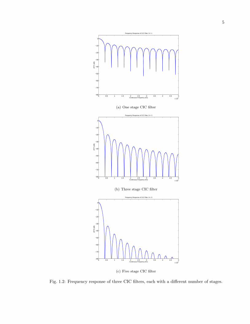
1.2 Frequency response of three CIC filters, each with a different number of stages. 5
1.3 Block diagram of a CIC decimator. . . . . . . . . . . . . . . . . . . . . . . . 6
1.4 Block diagram of a decimating CIC filter in which the downsampler has beenpushed before the comb cascade using a Noble identity. Notice that the combfilters now delay the input signal by M samples instead of RM samples asin fig. 1.3. . . . . . . . . . . . . . . . . . . . . . . . . . . . . . . . . . . . . . 6
1.5 Block diagram showing the processing from (1.2) using polyphase filters anddelay elements. The filtered signal is then downsampled. . . . . . . . . . . . 8
1.6 Block diagram showing a decimating polyphase filter after a noble identityhas been applied to the block diagram in fig. 1.5, pushing the downsamplersin front of the polyphase filters. This is the processing that will be performedafter the CIC filter in the design of this project. . . . . . . . . . . . . . . . . 9
2.1 A figure showing the role of each of the specifications outlined in Table 2.1. 11
2.2 Spectrum of the test signal that contains the four frequency components atF0 + W , F0 − W , F0 + δF , and F0 − δF . The first two are desired, whereasthe second two frequency components are undesired and should be filtered out. 14
2.3 Spectrum of the test signal after demodulation by cosine. . . . . . . . . . . 14
2.4 Top-level block diagram of the system. . . . . . . . . . . . . . . . . . . . . . 15
2.5 Frequency response of the CIC filter with five stages. At W , the frequencyof interest, the attenuation is about -0.56 dB. At W + δF , the first unwantedfrequency component, the attenuation is about -1.28 dB. . . . . . . . . . . . 16
2.6 Test spectrum after CIC filter has decimated it by 125. . . . . . . . . . . . . 16
2.7 Frequency response of the designed low-pass prototype filter. Notice thatthe stop-band attenuation is actually 80 dB. This is because the filter wasdesigned above specs to account for quantization error when fixed point co-efficients are used. . . . . . . . . . . . . . . . . . . . . . . . . . . . . . . . . 17

x
2.8 Frequency response of the quantized low-pass prototype filter. The frequencyresponse of the full precision filter is also shown for comparison. . . . . . . . 18
2.9 Spectrum of the fully decimated signal. This signal is sampled at the de-sired sample rate, FS,final = 100kHz, which is twice the symbol rate of thecommunications system. . . . . . . . . . . . . . . . . . . . . . . . . . . . . . 18
3.1 Block diagram of the top level in the design hierarchy. The decimation factorgenerics for each filter are specified. The q1 and q2 blocks shown are quan-tizers. They perform quantization using truncation, keeping the upper bitsof the input. . . . . . . . . . . . . . . . . . . . . . . . . . . . . . . . . . . . . 22
3.2 The top-level of the CIC filter hierarchy. . . . . . . . . . . . . . . . . . . . . 23
3.3 Integrators module structure. This structure was generated using a generatefor loop based on the N stages cic generic of the top-level module. Registersare shown as a block with a triangle on the bottom. . . . . . . . . . . . . . 24
3.4 Block diagram of the downsampler module in the CIC filter hierarchy. Thestart ctrl module enables the ce ctrl module to grab the first good sample. . 24
3.5 A block diagram of the comb filter cascade. The M parameter is called thedifferential delay. There is no generic specifying this parameter; it is fixed attwo for this design. . . . . . . . . . . . . . . . . . . . . . . . . . . . . . . . . 25
3.6 Block diagram showing the top level of the hierarchy for the polyphase FIRfilter. . . . . . . . . . . . . . . . . . . . . . . . . . . . . . . . . . . . . . . . . 26
3.7 Block diagram showing the structure of the FIR taps module in the polyphaseFIR filter design hierarchy. . . . . . . . . . . . . . . . . . . . . . . . . . . . 27
4.1 Plot showing quantized outputs from the MATLAB simulation alongside thecorresponding outputs from the post PAR top level VHDL simulation. . . . 31
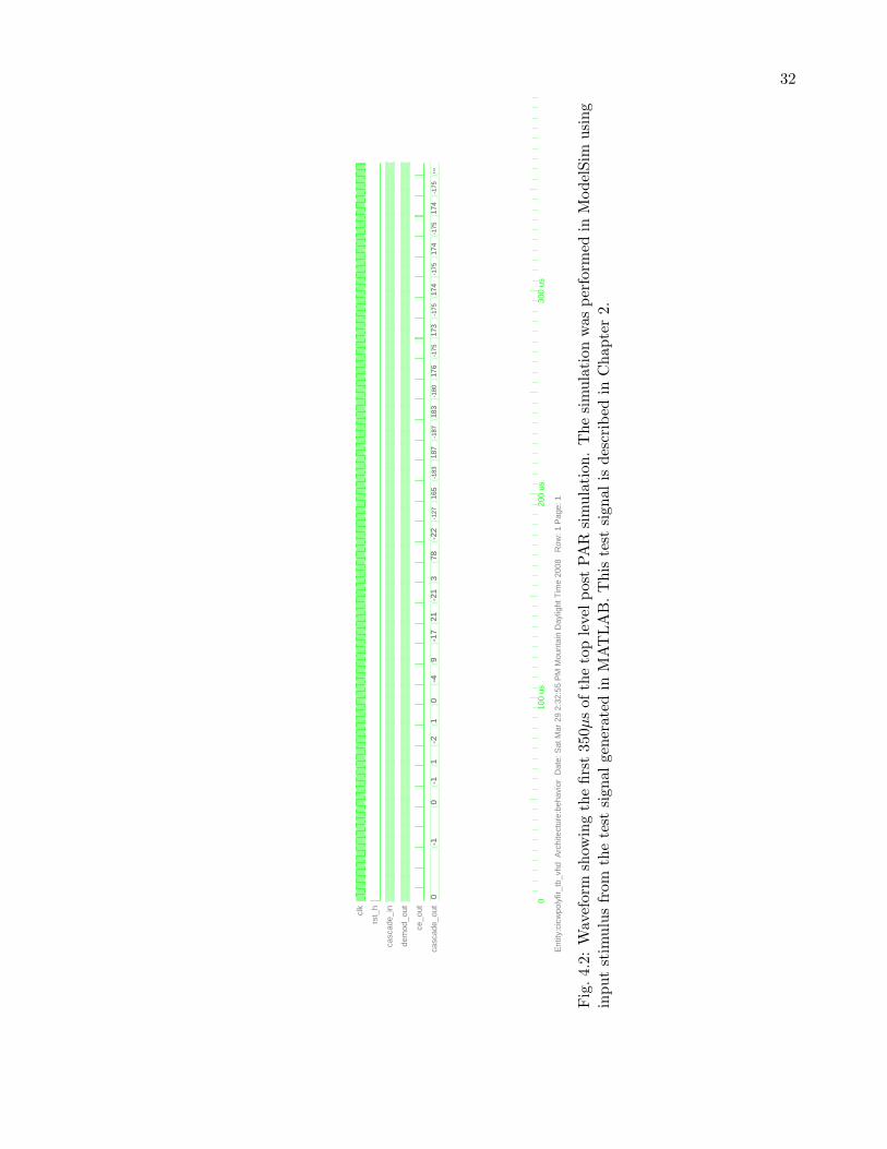
4.2 Waveform showing the first 350μs of the top level post PAR simulation. Thesimulation was performed in ModelSim using input stimulus from the testsignal generated in MATLAB. This test signal is described in Chapter 2. . . 32
4.3 An excerpt of a Xilinx ISE 9.1i PAR report outlining the target FPGA uti-lization for the VHDL design. The target FPGA here is a Xilinx Virtex595sxt. . . . . . . . . . . . . . . . . . . . . . . . . . . . . . . . . . . . . . . . 33

1
Chapter 1
Background
1.1 Introduction
In recent years, there has been a great demand for wireless communications technology.
As a result of this increasing demand, several new wireless communication standards have
been created and put into use. With the advent of all of these different wireless standards, it
is desirable to have a radio receiver that is capable of communicating with several different
standards. This requires a radio to be able to reconfigure its features (demodulation, error
correction, etc.) according to the type of communications standard it is trying to interact
with. Another advantage of a radio that can be reconfigured is the fact that the radio does
not become obsolete with the creation of a new wireless standard. A radio that can be
reconfigured is called a software radio.
1.2 Software Radios
In order for a radio to be able to reconfigure itself based on the signals it is receiving,
it has to be largely defined with software. In other words, these types of radios are able to
reconfigure the hardware using software. This terminology is somewhat vague. How much
flexibility does a radio need to have in order to be called a software radio? The following
quote helps to define what it means to be a software radio.
A good working definition of a software radio is a radio that is substantially
defined in software and whose physical layer behavior can be significantly altered
through changes to its software [1, pg. 2].
As an example, a radio that utilizes a digital signal processor or microprocessor is not
necessarily a software radio. On the other hand, if a radio defines its modulation, error

2
correction and encryption in its software and also exhibits some flexibility over the radio
frequency (RF) hardware, it is clearly a software radio. Generally, a software radio refers
to a radio that is flexible with respect to the software, but the software operates on a static
hardware platform.
In order to maximize flexibility, a software radio receiver digitizes the received signal as
soon as possible to utilize the flexibility of digital signal processing (DSP). This is usually
done after an analog front end filters, amplifies, and mixes the signal to an intermediate
frequency (IF). The signal is then digitized and translated to baseband using a digital down
converter (DDC).
1.3 Project Scope
In this project, hardware will be designed and implemented that will perform an IF to
baseband conversion of a received signal. This hardware is intended for use in a software
radio. The functions that this hardware will perform are outlined below:
• Demodulation: The incoming signal will be translated from an intermediate frequency
to baseband.
• Decimation: The baseband signal will be filtered and downsampled to a more man-
ageable sampling rate.
Even with RF hardware partially demodulating the carrier signal to an intermediate
frequency, the sample rate of the system is still fairly high (about 100 - 500 MHz). This
being the case, a DSP chip will not be able to process the data coming from the analog
to digital converter (ADC) fast enough for a real time setting. This leaves either a field
programmable gate array (FPGA) or an application specific integrated circuit (ASIC) as
the target hardware for this project. Being in a University setting, an FPGA is the more
economical choice. Using an FPGA is desirable also because they can be reprogrammed on
the fly, coinciding with the reconfigurability required of a software radio.
Having determined that an FPGA will be used to perform the processing, very high
speed integrated circuit hardware description language (VHDL) will be used to implement

3
the hardware. VHDL was chosen since the use of generic modules and generate for loops (a
VHDL construct, discussed in detail in Chapter 3) will make the FPGA design flexible and
reconfigurable. With generic modules, the processing the FPGA performs can be greatly
altered or modified by simply changing the generic values of the top level design. Generate
for loops that are based on the generic values will then be used to create the structures of
the decimating filters.
For this design, the intermediate frequency is assumed to be 14 of the ADC sample rate.
This imposes some restrictions on the analog front end of the receiver. These restrictions on
the RF hardware make the demodulation circuitry multiplier free (see Chapter 2 for more
details). Another implication of these simplifying assumptions is that the received signal
is going to be oversampled by a large factor, leading to a high decimation factor required
of the DDC hardware. For example, if FS = 100MHz and the bandwidth of the desired
signal is 100 kHz, the decimation factor will be in the neighborhood of 1000.
Since the DDC hardware is going to need to decimate the input signal by a large factor,
the decimation will be broken up into a cascade of two to three decimating filters. The first
filter in the cascade is going to have to operate at a fairly high sample rate. Because of this,
the first filter in the cascade was chosen to be a cascaded integrator-comb (CIC) filter [1–4].
These filters have a low-pass response and are multiplier-free. With applications of the
Noble identities, these filters can also be made to decimate or interpolate. After the CIC
filter partially decimates the input signal, a more complicated filter can be implemented
to perform the rest of the decimation. Due to this, the next filter(s) in the cascade were
chosen to be polyphase decimating filters [2, 5]. The theory of each of these types of filters
are described in the following sections.
1.4 CIC Filter Theory
As mentioned before, a cascaded integrator comb (CIC) filter is a multiplier free filter
that has a low-pass response1. These filters can also be used as a decimating filter. As the
1This development follows closely from [1].

4
name suggests, a CIC filter is constructed by cascading two simple filter structures together:
combs and integrators. Figure 1.1 shows the structure of each of these building blocks.
The more integrator and comb filters that are cascaded together, the better the CIC
filter does at filtering. The CIC filter exhibits better stopband attenuation, but the sinc
shaping in the passband is more pronounced. In essence, a cascade of an integrator and a
comb filter is equivalent to an FIR filter with an impulse response of a rectangular window
of length M . This translates to a sinc shaped filter response. Figure 1.2 shows the frequency
response of CIC filters with one, three, and five stages to further illustrate this point.
In order to make this a decimating filter, N integrator filters are cascaded together
followed by N comb filters and finally by a downsampler. Figure 1.3 shows a block diagram
of this cascade.
The transfer function of the decimating CIC filter shown in fig. 1.3 is
H(z) =
(1 − z−RM
1 − z−1
)N
,
leading to the frequency response
H(ω) =
(sin
(ωRM
2
)sin
(ω2
))N
,
where R is the decimation factor of the filter, M is the differential delay (or the number of
samples to delay the input signal in the comb stages), and N is the number of stages in the
CIC. Using one of the Noble identities, the downsampler can be pushed before the comb
filter cascade. This is shown in fig. 1.4.
IN OUT
z−1
(a) Integrator Filter
IN OUT
z−M
-
(b) Comb Filter
Fig. 1.1: Basic building blocks of a CIC filter.
5
0 0.5 1 1.5 2 2.5 3 3.5 4 4.5 5
x 106
−80
−70
−60
−50
−40
−30
−20
−10
0
Frequency Response of CIC Filter, N = 1
Continuous Frequency (Hz)
|FF
T| (
dB)
(a) One stage CIC filter
0 0.5 1 1.5 2 2.5 3 3.5 4 4.5 5
x 106
−80
−70
−60
−50
−40
−30
−20
−10
0
Frequency Response of CIC Filter, N = 3
Continuous Frequency (Hz)
|FF
T| (
dB)
(b) Three stage CIC filter
0 0.5 1 1.5 2 2.5 3 3.5 4 4.5 5
x 106
−80
−70
−60
−50
−40
−30
−20
−10
0
Frequency Response of CIC Filter, N = 5
Continuous Frequency (Hz)
|FF
T| (
dB)
(c) Five stage CIC filter
Fig. 1.2: Frequency response of three CIC filters, each with a different number of stages.

6
INN
IntegratorsN
Combs (RM delay)↓ R OUT
Fig. 1.3: Block diagram of a CIC decimator.
The structure shown in fig. 1.4 is desirable because in this configuration, the comb
cascade can operate at the lower sample rate. There are several advantages for using a
CIC filter. The first reason is that they are multiplier free, making them ideal for high
sample rate applications. Secondly, they can be organized such that they decimate the
incoming signal while at the same time filtering with a low-pass filter to avoid aliasing
in the frequency domain. One disadvantage of the CIC filter, however, is that they have
relatively large gain. The gain of a CIC filter is (RM)N . This leads to large accumulator
registers in the integrator stages when fixed-point arithmetic is used. If the bit width of the
accumulator registers is not sufficient to allow for the gain of the filter, they can overflow
and cause the filter to be unstable. It has been shown [6] that if the output bit width follows
Bout = Bin + N�log2 RM�, (1.1)
where Bout is the bit width of the CIC filter output and Bin is the bit width of the input to
the CIC filter, then the accumulators will not overflow and the filter will be stable. It can
be seen from (1.1) that the bit width of the accumulators can be quite large. With modern
FPGAs however, registers are plentiful. Due to this, full precision according to (1.1) will
be kept throughout the CIC filter and quantized before the next filter processes the data.
Another disadvantage of the CIC filter is that it has a sinc shaped frequency response.
This could lead to unwanted attenuation in the passband of the filter. To correct this, a
INN
Integrators↓ R
NCombs (M delay)
OUT
Fig. 1.4: Block diagram of a decimating CIC filter in which the downsampler has beenpushed before the comb cascade using a Noble identity. Notice that the comb filters nowdelay the input signal by M samples instead of RM samples as in fig. 1.3.

7
CIC correction filter [7] usually follows a decimating CIC filter to correct the unwanted
droop. The filter that will follow the CIC filter and decimate the signal to its final desired
sample rate is a polyphase FIR filter.
1.5 Polyphase FIR Filter Theory
A decimating FIR filter is constructed by taking a prototype filter (a low-pass filter
with a cutoff frequency near πM
radians or 12M
cycles, where M is the desired decimation
factor) and decomposing the coefficients into several shorter polyphase filters in such a
way that a Noble identity can be invoked to push the downsampling operation before the
polyphase representations of the filter2. This is desirable for this application for two main
reasons:
1. The polyphase filters operate at the slower sample rate.
2. A single FIR filter can be used to both downsample and filter the input signal to avoid
aliasing in the downsampling process.
The first step in constructing a polyphase representation is to decompose the coeffi-
cients, h(n), into M different polyphase filters, each with NM
taps where N is the number
of taps in the prototype filter and M is the decimation factor. This decomposition can be
visualized by writing the Z-transform of h(n) in the following way:
H(Z) =
h(0) + h(M + 0)z−M + h(2M + 0)z−2M + . . .
+h(1)z−1 + h(M + 1)z−(M+1) + h(2M + 1)z−(2M+1) + . . .
+h(2)z−2 + h(M + 2)z−(M+2) + h(2M + 2)z−(2M+2) + . . .
. . .
+h(M − 1)z−(M−1) + h(2M − 1)z−(2M−1) + . . .
2This discussion follows closely from [2] and [3].

8
=
H0(zM )
+z−1H1(zM )
+z−2H2(zM )
. . .
+zM−1HM−1(zM ).
(1.2)
Now, each row in (1.2) can be looked at as a polynomial in zM , with each row offset
with a one sample delay from the row above it. Each row now represents a polyphase filter.
Figure 1.5 shows a block diagram that performs the same processing as (1.2) and then
downsamples the signal by M .
We are now in a position to apply a Noble identity and push the downsampler in front
of the polyphase filters. The block diagram showing this operation is shown in fig. 1.6. The
sequence of delay elements and downsamplers preceding the polyphase filters in fig. 1.6 is
often replaced with a commutator switch.
One or two cascaded stages of these polyphase filters will follow the decimating CIC to
finish the decimation of the oversampled input signal coming from the ADC in the system.
This concludes the theory of the filters used in this project. There will be two polyphase
filters if the droop in the passband of the CIC causes enough distortion to require a CIC
compensation filter. If the droop in the passband is acceptable, however, there will only be
one decimating polyphase filter in the system.
IN
z−1 H1(zM )
H0(zM )
z−2
...
H2(zM )
...
z−(M−1) HM−1(zM )
↓ M OUT
Fig. 1.5: Block diagram showing the processing from (1.2) using polyphase filters and delayelements. The filtered signal is then downsampled.

9
IN
z−1 ↓ M H1(z)
H0(z)↓ M
z−2 H2(z)↓ M
......
...
z−(M−1) HM−1(z)↓ M
OUT
Fig. 1.6: Block diagram showing a decimating polyphase filter after a noble identity hasbeen applied to the block diagram in fig. 1.5, pushing the downsamplers in front of thepolyphase filters. This is the processing that will be performed after the CIC filter in thedesign of this project.
1.6 Conclusion
In this chapter, we have described a need for this project and given sufficient back-
ground theory to understand the terminology used in the following chapters of this report.
This chapter has also defined the DSP that is involved with this project and outlined the
processing that needs to be taken place for the DDC of the incoming software radio signal.
The following chapters will describe the design (in MATLAB) of the filters and the VHDL
implementation and verification. The final chapter will summarize the work completed
on this project and outlines possible future work that is related to the work done in this
project. Appendix B and Appendix C show the MATLAB and VHDL listings of this design,
respectively. These appendices are included for reference.

10
Chapter 2
MATLAB Design
2.1 Introduction
As a first step in the design process, a preliminary MATLAB design was made. The
intended FPGA system was simulated using MATLAB before the digital system was imple-
mented using VHDL. This step in the design process served several purposes. First, a more
thorough understanding of how the hardware should work was attained when this step was
carried out. Second, intermediate signals from the MATLAB design of the system can be
input into a VHDL testbench and used to stimulate certain parts of the design. Third, the
MATLAB design was used to determine the tolerable precision of the polyphase FIR filter
coefficients. Fourth, the performance of the system can be visualized and verified much
easier in a MATLAB environment than a VHDL environment. Because of these reasons, a
preliminary MATLAB design was implemented.
2.2 Specifications
To verify correct functionality of the filters in the digital down conversion processing
chain, some general requirements of the spectrum of the incoming signal had to be defined.
These specifications are shown in Table 2.1. Note that these specifications are only to test
a single configuration of the software radio. It is necessary to specify a set of specifications
so that the hardware can be verified for this class of signals. This being said, a main goal
of the software radio will be to successfully process other, different types of signals when it
is implemented in a communications system.
To further visualize each specifications role and importance, fig. 2.1 shows an example
spectrum.

11
Table 2.1: Input signal specifications.Specification Description Value
FS The sampling frequency of the ADC used inthe system.
100 MHz
F0 The carrier frequency of the desired sig-nal. For this design, this specification isfixed at 1
4FS . This makes the demodulationmultiplier-less (see discussion below).
14FS = 25 MHz
W This specifies the one-sided bandwidth of thedesired spectrum.
50 kHz
ΔF Frequency separation between wanted signaland unwanted signals in the spectrum.
125 kHz
δF Transition band required of the anti-aliasingfilter for the initial decimation.
25 kHz
F (Hz)
|H(F )|
Antialiasing filter response
F0 F0 + W F0 + ΔFF0 − ΔFδF
Fig. 2.1: A figure showing the role of each of the specifications outlined in Table 2.1.

12
Choosing F0 to be 14FS makes the demodulator multiplier-less in the following way.
Normally, the demodulator modulates by sin(·) and cos(·) at the carrier frequency F0, but
since F0 = 14FS , the modulators can be simplified:
cos (2πF0n) = cos
(2π
4FSn
)
= cos(π
2FSn
)
=
⎧⎪⎪⎪⎪⎨⎪⎪⎪⎪⎩
1 n = 0, 4, 8, . . .
0 n = 1, 3, 5, . . .
−1 n = 2, 6, 10, . . .
. (2.1)
The demodulator in the in-phase branch of the receiver can be similarly simplified:
sin(π
2FSn
)=
⎧⎪⎪⎪⎪⎨⎪⎪⎪⎪⎩
1 n = 1, 5, 9, . . .
0 n = 0, 2, 4, . . .
−1 n = 3, 7, 11, . . .
. (2.2)
It is important to note, though, that this F0 is not necessarily the true carrier frequency
of the desired signal. It is more likely that F0 is going to be an intermediate frequency where
an analog front end to the digital receiver has performed a partial demodulation. So to be
more precise, F0 is the intermediate carrier frequency.
Another important specification that needs to be fixed for this example scenario is
the overall decimation factor. Suppose that a square root raised cosine (SRRC) pulse
shape is used with an excess bandwidth (α) of 100%. Also assume that we want the final
downsampled signal to be oversampled by a factor of two, that is:
FS,final = 2RS ,
where RS is the symbol rate and FS,final is the final sampling rate after the decimation
stages. Because of the SRRC pulse shape, the bandwidth of the signal (W ) can be related

13
to the sampling rate:
W =1 + α
2TS
=1
TS
= RS ,
so that
FS,final = 2RS = 2W = 100kHz,
and finally
DTOT =FS
FS,final
=100MHz
100kHz= 1000,
where DTOT is the overall decimation factor.
Notice that DTOT can be factored as 23 · 53 = 8 · 125. This is convenient because
it means that each decimation stage is able to decimate by an integer factor. The CIC
filter will decimate by a factor of 125, leaving the polyphase FIR filter to decimate by the
remaining factor of 8.
To test the design of the filters and to verify their proper operation, a test signal
consisting of a sum of cosines at four different frequencies will be processed by the filter
cascade. The four different frequencies were chosen to be: F0 + W , F0 − W , F0 + δF ,
and finally F0 − δF . Obviously, after the filtering and downsampling stages, the first two
frequency components should be intact while the second two frequency components should
be filtered out. Figure 2.2 shows the test signal that is applied to the system.
Figure 2.3 shows the signal after the test signal was demodulated with the sequence of
{±1, 0} shown in (2.1).
After demodulation, the signal will be downsampled and decimated by a factor of 125
by the CIC filter. Immediately following this decimation, a polyphase filter will filter and
downsample the signal by the remaining factor of 8. Figure 2.4 shows a block diagram of
the top level system.
2.3 CIC Filter Design
Having defined the specifications of this test spectrum, the filters can be designed.
As discussed in Chapter 1, the demodulated signal will first be processed by a CIC filter.

14
2.49 2.492 2.494 2.496 2.498 2.5 2.502 2.504 2.506 2.508 2.51
x 107
0
0.5
1
1.5
2
2.5
3x 10
4
X: 2.492e+007Y: 2.952e+004
X: 2.495e+007Y: 2.968e+004
X: 2.505e+007Y: 2.964e+004
X: 2.508e+007Y: 2.943e+004
Continuous Frequency (Hz)
|FF
T|
Modulated Signal
Fig. 2.2: Spectrum of the test signal that contains the four frequency components at F0+W ,F0−W , F0 + δF , and F0− δF . The first two are desired, whereas the second two frequencycomponents are undesired and should be filtered out.
0 5 10 15
x 104
0
0.5
1
1.5
2
2.5
3x 10
16
X: 4.997e+004Y: 2.546e+016
X: 7.515e+004Y: 2.146e+016
Demodulated Signal
Continuous Frequency
|FF
T|
Fig. 2.3: Spectrum of the test signal after demodulation by cosine.

15
INPUT demodCIC
↓ D cicFIR
↓ D firOUTPUT
Fig. 2.4: Top-level block diagram of the system.
At this stage in the downsampling process, the incoming signal is heavily oversampled
(FS/2 = 50MHz whereas W = 50kHz). This means that the main lobe of the CIC filter
has to be fairly narrow, requiring a high number of stages. Through experimentation, it
was found that a CIC filter with five stages had a sufficiently narrow main lobe. Figure 2.5
shows the frequency response of a CIC filter with five stages and a differential delay of two.
Notice that the CIC filter will not completely filter out the unwanted frequency compo-
nent, and also that it does attenuate the desired signal slightly. This attenuation, however,
is negligible (in this case) and does not affect the functionality of the receiver. This fil-
ter does, however, avoid aliasing before the downsampling operation because it filters out
everything except for the two signals that are close to baseband. The demodulated signal
after being CIC filtered and decimated by 125 is shown in fig. 2.6.
Since the effects of the sinc-shaping on the signal from the CIC signal are negligible,
there is no need to make the polyphase FIR filter a CIC correction filter [7] and it can
simply be designed as a low-pass filter.
2.4 Polyphase FIR Filter Design
After the decimation accomplished by the CIC filter, the two frequency components
that remain are separated enough in the spectrum that the polyphase FIR filter can properly
filter the remaining unwanted frequency components out of the spectrum while, at the same
time, downsampling to the desired sampling rate, FS,final.
Since the CIC filter decimated the signal by a factor of 125, W is now effectively at
(50 · 125)kHz = 6.25MHz in the spectrum while the unwanted frequency component lies
at (75 · 125)kHz = 9.375MHz at a sample rate of FS
125 = 800kHz. This being the case, the
prototype filter was designed to be a low-pass filter with a passband (Fpass) of 6.25MHz
and a stop-band (Fstop) of 9.375MHz. This filter was designed using a Chebyshev window

16
0 1 2 3 4 5 6 7
x 105
−80
−70
−60
−50
−40
−30
−20
−10
0
Frequency Response of CIC Filter, N = 5
Continuous Frequency (Hz)
|FF
T| (
dB)
Fig. 2.5: Frequency response of the CIC filter with five stages. At W , the frequencyof interest, the attenuation is about -0.56 dB. At W + δF , the first unwanted frequencycomponent, the attenuation is about -1.28 dB.
0 2 4 6 8 10 12 14 16 18
x 106
0
0.5
1
1.5
2
2.5x 10
14
X: 6.25e+006Y: 2.036e+014
X: 9.375e+006Y: 1.73e+014
Continuous Frequency (Hz)
|FF
T|
CIC decimated signal, Rcic
= 125
Fig. 2.6: Test spectrum after CIC filter has decimated it by 125.

17
with 60 dB of attenuation in the stop-band. To achieve the specified stop-band attenuation,
240 filter taps were used. Figure 2.7 shows the frequency response of the designed filter.
In the VHDL implementation, the filter coefficients are going to be represented as
two’s-complement signed integers. This means that the designed filter coefficients need to
be quantized. Sufficient precision needs to be maintained to keep the necessary stop-band
attenuation. After experimentation, it was determined that 14 bits of precision in the
coefficients were sufficient. Figure 2.8 shows the filter response of the filter with quantized
coefficients along with the full precision filter.
Using the designed prototype filter taps, a polyphase filter is created using the process
outlined in Chapter 1. In this case, there are 240 taps and a downsampling factor of eight,
so the polyphase filterbank will have eight filters, each with 30 (2408 ) taps (see fig. 1.6).
After the polyphase filter is designed, the CIC decimated signal is further filtered and
downsampled. Figure 2.9 shows the final, fully decimated signal. As you can see, the filter
cascade filters out all the unwanted signal components for this example spectrum and avoids
aliasing in the downsampling operations simultaneously.
0 5 10 15
x 106
−100
−90
−80
−70
−60
−50
−40
−30
−20
−10
0
Frequency Response of Prototype Filter, 240 taps
Continuous Frequency (Hz)
|FF
T| i
n dB
Filter responseF
pass
Fstop
Fig. 2.7: Frequency response of the designed low-pass prototype filter. Notice that thestop-band attenuation is actually 80 dB. This is because the filter was designed above specsto account for quantization error when fixed point coefficients are used.

18
0 5 10 15
x 106
−120
−100
−80
−60
−40
−20
0
Continuous Frequency
|FF
T| i
n dB
Quantized and Double Precision Magnitude Response 240 taps
Full PrecisionQuantized to 14 bits
Fig. 2.8: Frequency response of the quantized low-pass prototype filter. The frequencyresponse of the full precision filter is also shown for comparison.
0 2 4 6 8 10 12
x 107
0
2
4
6
8
10
12
14
16
18x 10
12
Continuous Frequency (Hz)
|FF
T|
Polyphase filtered signal, Rfir
= 8, Rcombined
= 1000
X: 5e+007Y: 1.68e+013
Fig. 2.9: Spectrum of the fully decimated signal. This signal is sampled at the desiredsample rate, FS,final = 100kHz, which is twice the symbol rate of the communicationssystem.

19
2.5 Conclusion
In this chapter, a test signal was created and the appropriate filters were designed
to properly process this signal. As you can see from the preceeding sections, the filters
designed properly filter and downsample the signal such that aliasing is avoided. Also, the
signal is decimated to the appropriate sample rate. The sample rate is low enough now
that something like a DSP chip can be used to incorporate further flexibility in the signal
processing that remains to make decisions on what symbols were sent.

20
Chapter 3
VHDL Design
3.1 Introduction
For reasons discussed in Chapter 1, the down conversion of the signal is performed in
an FPGA. This allows for the flexibility required of a software radio. In order to make the
design flexible, VHDL generics were incorporated into the design. In addition to generics,
generate for loops (which were based on the generic parameters) were used to generate the
structure of the filters. In order to accommodate the different sampling rates that are in
the design, one global clock signal is used to drive the flip flops. Clock enable signals are
then created and used to drive clock enabled flip flops for the slower sampling rate portions.
To implement the math functions required in the antialiasing filters, two’s-complement
signed, fixed point integer arithmetic is implemented on the FPGA. This facilitates the use
of the VHDL operators (+,-,*), thus enabling the use of generic adders and multipliers.
Also, initializing the FIR filter tap ROMs is done by loading them with files generated by
MATLAB. The generic values of the VHDL design are described next.
3.2 Generics
As mentioned in the previous section, one important aspect of the design are the
generic parameters. These are used to make the FPGA design flexible. In order to change
the behavior of the processing, one simply has to change the related generics. Table 3.1
outlines the generics that are used to describe the top level of the design hierarchy. These
generics then get mapped to the appropriate modules in the lower levels of the design
hierarchy.

21
Table 3.1: Description of generics.generic description
B casc in The input bit width of the processing chain,essentially the output bit width of the ADCused in the system.
B cic out The output bit width of the CIC filter and thebit width of the accumulators in the integratorstages.
D cic The decimation factor of the CIC filter.
N stages cic The number of stages in the CIC filter.
N poly taps The number of taps in the polyphase FIR fil-ter.
B poly coeffs The number of bits in the coefficients of theFIR filter.
B poly in The input bit width of the polyphase FIR fil-ter. This is effectively the number of bits toquantize the CIC filter output to before theFIR filter processes the data.
B poly out The full precision output of the polyphase FIRfilter. This is also the number of bits used inthe accumulator registers in the acc D mod-ules.
B casc out The output bit width of the filter cascade.This is a quantized version of the FIR filteroutput.
D fir The decimation factor of the FIR filter. Alsothe number of elements in the tap ROM mod-ules.
B rom addr The number of bits in the tap ROM moduleaddress. This is log2(D fir).

22
As you can see, the behavior of the VHDL design can be greatly modified by simply
modifying the generic values. It is important to note, however, that changing a generic
changes the entire design. This means that the design needs to be synthesized, mapped,
and routed again. This can be a potential problem for a software radio. One possible work-
around is to have several different FPGA configurations (corresponding to different generic
values) in on-board memory. The software can then decide which programming image to
use to reprogram the FPGA with. A description of the VHDL modules used in the design
hierarchy follows this section.
3.3 Design Hierarchy
The VHDL design has several different levels of hierarchy. This section explains each
level of the hierarchy in detail. Figure 3.1 shows the top level of the hierarchy.
The following sections descend into the design hierarchy supplying descriptions of each
module.
3.3.1 Demodulator
As shown in fig. 3.1, the demodulator module is the first block in the processing chain.
For the reasons discussed in Chapter 2, there are no multipliers in the demodulator circuitry.
This module assigns the output according to a two bit counter and (2.1).
INPUT demodCIC
↓ D cicq1
FIR↓ D fir
q2 OUTPUT
Fig. 3.1: Block diagram of the top level in the design hierarchy. The decimation factorgenerics for each filter are specified. The q1 and q2 blocks shown are quantizers. Theyperform quantization using truncation, keeping the upper bits of the input.

23
3.3.2 CIC Hierarchy
The CIC filter is broken down into four different levels of hierarchy. The top level of
the CIC hierarchy is shown in fig. 3.2.
A few important things to note about the CIC filter design are:
• The input is sign extended to B cic out bits, and this amount of precision is kept
throughout.
• B cic out is assumed to be sufficient for the accumulations that are occurring in the
integrator stages. In other words, the adders in the CIC filter implementation have
no carry bits.
• The CIC filter is pipelined: the accumulator registers are arranged in such a way that
there is only one addition in between the register layers [8]. Also, pipeline registers
were added in the comb stages in order to only require one subtraction operation in
between registers.
The next sections describe the Integrators, Downsample, and Combs modules shown
in fig. 3.2.
CIC Integrators
The integrators module of the CIC filter is simply a cascade of several accumulators.
How many accumulators to cascade is governed by the N cic stages generic. A generate for
loop based on this generic is used to cascade the appropriate number of accumulators in
this design. Figure 3.3 shows a block diagram of the structure of this module.
It is important to note also that the integrators have to operate at the highest sample
rate, therefore, it is critical that they are sufficiently optimized. The next section shows the
design of the downsampler block shown in fig. 3.2.
CIC IN Integrators ↓ D cic Combs CIC OUT
Fig. 3.2: The top-level of the CIC filter hierarchy.

24
INTS IN . . . INTS OUT
Fig. 3.3: Integrators module structure. This structure was generated using a generate forloop based on the N stages cic generic of the top-level module. Registers are shown as ablock with a triangle on the bottom.
CIC Downsampler
As mentioned in sec. 3.1, the downsampling operation in the CIC filter is accomplished
using a clock enabled register. Two controllers are also in the downsampler module. One
control accounts for the latency due to the accumulator registers and outputs an enable
signal to the second controller to signal it when to start counting. This ensures that the
clock enabled flip flop passes on the first good sample to the rest of the design because
it has properly waited for the first sample to propagate through the accumulators. The
second controller generates the clock enable signal that drives the comb flip flops and some
of the flip flops in the polyphase FIR filter. The first controller is based on the N stages cic
generic whereas the second controller counts clock cycles according to the D cic generic.
Figure 3.4 shows a block diagram of the downsampler module.
After the downsampling operation, the data rate is divided by the D cic generic. This
means that the comb sections (and the first half of the FIR filter) can operate at the slower
rate.
CIC Combs
The final stage of the CIC filter is a cascade of N comb filters. These filters operate
clk start ctrl ce ctrl
IN
cereg OUT
d
ce
q
Fig. 3.4: Block diagram of the downsampler module in the CIC filter hierarchy. Thestart ctrl module enables the ce ctrl module to grab the first good sample.

25
at FS
D cic . As in the CIC integrator stages, a generate for loop based on the N stages cic
generic was used to cascade the desired number of comb filters together. A block diagram
of the structure of the comb filter cascade is shown in fig. 3.5.
As you can see from fig. 3.5, pipeline registers were added to reduce the combinational
path delay. With the extra register layers, there is only one subtractor in between a register.
After the comb stage, the signal has been filtered and downsampled by a factor of D cic.
After the CIC filter, the signal needs to be downsampled to the final sample rate. This is
accomplished with a polyphase FIR filter.
3.3.3 FIR Filter Hierarchy
The polyphase FIR filter is the final step in the digital down conversion of the signal. As
mentioned before, after the CIC filter partially decimates the input signal, it gets quantized
and then input to the FIR filter. This is so that the FIR filter can maintain full precision
throughout the filtering operations. Also, to make the FIR filter flexible, tap ROM modules
are loaded from text files. This design method makes it easy to design filter coefficients in
MATLAB or another software tool and load them into the VHDL design. A block diagram
of the top level of the FIR filter hierarchy is shown in fig. 3.6.
As you can see from fig. 3.6, the top level of the polyphase FIR filter hierarchy consists
simply of the controllers that are needed to feed the signals needed to do the filtering into the
FIR taps block. The FIR taps block is where the filtering actually takes place. Descriptions
of the controllers shown are given here:
COMBS IN
z−M
. . .
z−M
COMBS OUT
- -
Fig. 3.5: A block diagram of the comb filter cascade. The M parameter is called thedifferential delay. There is no generic specifying this parameter; it is fixed at two for thisdesign.

26
enablecontrol
cecontrol
CE OUT
addrcontrol
DATA IN
FIRtaps
DATA OUT
Fig. 3.6: Block diagram showing the top level of the hierarchy for the polyphase FIR filter.
enable control This controller serves much the same purpose as that of the start ctrl con-
troller shown in fig. 3.4. Namely, it outputs an enable signal to the ce control module
signaling it when the first good sample has arrived. The major difference between
start ctrl and enable control is that enable control counts the clock enable signal
output from the downsampling module in the CIC filter instead of the global clock
signal. This controller accounts for the latency introduced by the pipeline registers in
the comb section of the CIC filter.
ce control This controller uses both D cic and D fir to determine how many cycles of the
global clock to count before its clock enable signal is output. Note that this controller
counts only the global clock, it does not depend on the clock enable controller from
the downsample module in the CIC filter.
addr control This controller is a simple down counter that is used to address the tap
ROMs in the FIR taps module. It is important to note that this counter can count
down from an arbitrary number, it does not have to be a power of two.
The following section describes the structure and functionality of the FIR taps module
shown in fig. 3.6.
FIR Taps Module
The FIR taps module is the heart of the polyphase FIR filter. This is where the

27
downsampling and filtering takes place. In a usual polyphase filter bank implementation,
there would be several filters operating in parallel (the number of filters is equal to the
decimation rate of the filter, in this case, this is described by the D fir generic). In order
to save resources on the FPGA, this structure was “collapsed” into one filter. This was
accomplished by using tap ROM modules that hold D fir coefficients and modules that
accumulate the tap multiplier outputs for D fir cycles [9]. This accumulation is where the
effective downsampling operation takes place as well. Figure 3.7 shows the block diagram
of this “collapsed” polyphase FIR implementation. It is also important to note that the
structure was implemented using a generate for loop based on the N poly taps generic.
Some notes about the design of the FIR taps module are discussed here. The ACCDi
modules shown in fig. 3.7 accumulate their input for D fir cycles. This is where the down-
sampling operation takes place in the filter. Full precision is kept throughout the filter
and quantized at the end. Full precision is kept in the following way: first, the output bit
width of the multiplier is the sum of the bit widths of the two inputs (in terms of generics,
this is B rom coeffs + B poly in). Second, enough guard bits in the accumulator inside the
ACCDi modules are added to accommodate both for the accumulation and the adder chain
that follows. This is done to avoid having to implement carry chain logic through the adder
chain. The bit width of the accumulator registers in the ACCDi modules is set using the
generic B poly out.
IN
ROM0
ACCD0
ROM1
ACCD1
. . .
. . .
. . .
ROMN
ACCDN
OUT
Fig. 3.7: Block diagram showing the structure of the FIR taps module in the polyphaseFIR filter design hierarchy.

28
3.4 Conclusion
This chapter summarized the key points and design methodologies used in translating
the DSP design discussed in Chapter 2 into an FPGA design using VHDL. This VHDL
implementation obtains the flexibility required of a software radio using the generics shown
in Table 3.1. The hierarchy of the VHDL design was then summarized and described. The
next topic to be discussed is the method of verification used in the design process.
29
Chapter 4
Verification
4.1 Introduction
In this chapter, post place and route (PAR) simulations of the VHDL design are com-
pared with outputs from the MATLAB design to verify the correct functionality of the
synthesized, placed, and routed VHDL design.
Using Xilinx ISE 9.1i software tools1, the VHDL design was synthesized to several
FPGA targets. The post PAR simulations discussed in this chapter used a Virtex5-95sxt
FPGA as the target. ModelSim2 simulation software was used to perform the simulations.
4.2 Verification Method
In order to verify the VHDL design, intermediate signals from the MATLAB design
were quantized and written to files. These files were then read into a VHDL testbench
(using the VHDL textio package) and used to stimulate the design. Next, the VHDL
module output was written to a file to compare with the corresponding MATLAB signal.
For example, if the CIC filter implementation was to be tested, the demodulator output
from MATLAB would be quantized and written to a file. Then the testbench would read in
this file and use it to stimulate the CIC filter. The output of the CIC filter module would
then be written to a file. Finally, the CIC filter output from the MATLAB simulation could
be quantized and compared with the VHDL output.
Using this verification method, a simulation was conducted on the top level of the
VHDL design hierarchy. Using the test signal described in Chapter 2 as stimulus, the final
downsampled signal from the VHDL module matched exactly to the same signal from the
1© Xilinx Inc. 1995-20072© Mentor Graphics Corporation 2006

30
Table 4.1: Generic values used to generate fig. 4.2.generic value
B casc in 14
B cic out 54
D cic 125
N stages cic 5
N poly taps 30
B poly coeffs 14
B poly in 26
B poly out 50
B casc out 24
D fir 8
B rom addr 3
MATLAB simulation (as long as the MATLAB signal was quantized to the same fixed point
precision). Figure 4.2 shows the post PAR ModelSim simulation results. Table 4.1 shows
the generic values used for the simulation shown in fig. 4.2.
As you can see from fig. 4.2, the output signal changes at a much slower rate than
the input signal. It is important to note also, that the ce out signal shown in the figure is
also an output of the system. This is so that the processing that follows the decimation
can be synchronized to the output of the FPGA. Figure 4.2 also verifies that the design
meets the desired sampling rate of the system. In other words, the integrator section of
the CIC filter is able to operate at the desired frequency of 100MHz. In order to verify
the functionality of the system however, the output shown in fig. 4.2 needs to be compared
with the equivalent MATLAB signal. This comparison is shown in fig. 4.1.
As you can see from fig. 4.1, the VHDL implementation and the MATLAB simulation
perform the same desired processing of the test signal. A comparison of the VHDL output
from fig. 4.2 with the VHDL output from fig. 4.1 can also be used as further verification.
4.3 FPGA Utilization
For reference, a Xilinx ISE 9.1i PAR report that summarizes the utilization of the target
FPGA is included in fig. 4.3. Note that the processing that has been described throughout
this report has been for a one-dimensional signal (e.g., BPSK or PAM).

31
0 5 10 15 20 25 30 35−200
−150
−100
−50
0
50
100
150
200
Time (samples)
Qua
ntiz
ed O
utpu
ts
MATLAB Simulation Vs. VHDL Simulation
MATLAB outputVHDL output
Fig. 4.1: Plot showing quantized outputs from the MATLAB simulation alongside thecorresponding outputs from the post PAR top level VHDL simulation.
32
0-1
0-1
1-2
10
-49
-17
21-2
13
78-2
2-1
2716
5-1
8318
7-1
8718
3-1
8017
6-1
7517
3-1
7517
4-1
7517
4-1
7517
4-1
7517
4
010
0 us
200
us30
0 us
clk
rst_
h
casc
ade_
in
dem
od_o
ut
ce_o
ut
casc
ade_
out
0-1
0-1
1-2
10
-49
-17
21-2
13
78-2
2-1
2716
5-1
8318
7-1
8718
3-1
8017
6-1
7517
3-1
7517
4-1
7517
4-1
7517
4-1
7517
4
Ent
ity:c
icw
poly
fir_t
b_vh
d A
rchi
tect
ure:
beha
vior
Dat
e: S
at M
ar 2
9 2:
32:5
5 P
M M
ount
ain
Day
light
Tim
e 20
08
Row
: 1 P
age:
1
Fig
.4.2
:W
avef
orm
show
ing
the
firs
t350μ
sof
the
top
level
pos
tPA
Rsi
mula
tion
.T
he
sim
ula
tion
was
per
form
edin
Model
Sim
usi
ng
input
stim
ulu
sfr
omth
ete
stsi
gnal
gener
ated
inM
AT
LA
B.T
his
test
sign
alis
des
crib
edin
Chap
ter
2.

33
Device Utilization Summary:
Number of BUFGs 2 out of 32 6%
Number of DSP48Es 60 out of 640 9%
Number of External IOBs 41 out of 640 6%
Number of LOCed IOBs 0 out of 41 0%
Number of RAMB18X2s 30 out of 244 12%
Number of Slice Registers 6949 out of 58880 11%
Number used as Flip Flops 6949
Number used as Latches 0
Number used as LatchThrus 0
Number of Slice LUTS 6988 out of 58880 11%
Number of Slice LUT-Flip Flop pairs 11039 out of 58880 18%
Fig. 4.3: An excerpt of a Xilinx ISE 9.1i PAR report outlining the target FPGA utilizationfor the VHDL design. The target FPGA here is a Xilinx Virtex5 95sxt.
If a two-dimensional signal such as QPSK or QAM needs to be processed, an in-phase
processing branch needs to be included. Seeing as the processing would be identical for
the in-phase branch, these utilization reports need to be roughly doubled if a signal that
requires an in-phase branch is required.
One thing to note about fig. 4.3 is that this design uses 60 DSP48 blocks when there
are only 30 taps in the FIR filter. This is because in this design, the multiplication that
takes place requires a precision that is above the specification of the DSP48 block, so two of
these blocks have to be used for each multiplication in the FIR filter.
As it can be seen from fig. 4.3, this design uses only a small fraction of the resources
available for the target FPGA. Even if a QAM or QPSK signal needs to be processed, this
design would only utilize about 20% of the resources available. This opens up the possibility
of some of the downstream processing also being done on the FPGA.
4.4 Conclusion
In this chapter, the VHDL design and the MATLAB design were compared to verify
the functionality of the VHDL implementation. The method of verification was described

34
and then put to use to verify the functionality of the VHDL implementation. Furthermore,
this chapter described the device utilization as reported by the Xilinx ISE 9.1i tool.
35
Chapter 5
Summary and Future Work
5.1 Introduction
FPGA-based hardware that will take a software radio signal as input and decimate it
to the desired sampling rate has been designed, implemented, and verified. This design is
planned to be the first processing element in a processing chain that will make up a software
radio receiver. MATLAB was used to simulate the design at a high level and then VHDL
was used to implement the design on an FPGA. Successful post PAR simulations have been
obtained for several different FPGAs of the Xilinx Virtex family.
5.2 Work Completed
The scope of this project has been to design, implement, simulate, and verify the
hardware design summarized above. A summary of the work completed is shown below.
• Development of DSP theory: Decimating filter architectures and applications were
studied. As a result, a cascade of a CIC filter and a polyphase FIR filter was decided
to be designed and implemented. Initially, the polyphase FIR filter was going to be
made into a CIC correction filter, but later in the design process this was deemed
unnecessary.
• DSP Design: After the general structure of the DSP processing was established, the
filters had to be designed. Experiments were conducted using MATLAB to decide on
filter parameters such as:
- The number of stages in the CIC.
36
- The polyphase filter specifications: Passband frequency, cutoff frequency, and
stopband attenuation.
- Polyphase filter design: The polyphase FIR filter was designed using an ideal
frequency response and windowing using a Chebyshev window.
• MATLAB simulation: After the filters were designed, a MATLAB script was writ-
ten that simulated the cascade of the two filters. A test signal that would simulate
a realistic input signal was created and ran through the filter cascade. Several in-
termediate signals were quantized and written to files in order to verify the VHDL
implementation.
• VHDL implementation: The filter cascade was implemented using VHDL. The use of
generics and generate for loops allowed for the flexibility required of hardware used
in a software radio.
• Verification: In order to deal with the fact that several sampling rates were present
in this design, multi-cycle path specifications had to be input into the Xilinx tools to
verify that the design would meet timing requirements (see Appendix A). The VHDL
implementation was synthesized, placed and routed, and thoroughly simulated using
the MATLAB signals mentioned above. Finally, the VHDL output was compared
with the MATLAB simulation to ensure that the FPGA would perform the correct
processing on the input signal.
In summary, some of the necessary hardware for a software radio receiver has been
designed. Since the hardware is targeted for an FPGA and was written in VHDL, the
design is flexible and portable. The VHDL code has also been commented to allow for
future work on the design if needed. The MATLAB script used to verify the DSP design is
also used to simplify the design process. In particular, a MATLAB script has been written
that writes the coefficients of the FIR filter to several text files such that they can easily be
loaded into the VHDL modules.

37
5.3 Future Work
The first major area of future work in regards to this project consists of verifying
the design in an actual FPGA. Because of time and budget constraints, this has not been
accomplished at the present time. There are also several other areas of future work that
are related to this project.
The scope of the project discussed in this report consists of only one of several hardware
elements that are needed for a software radio receiver. This being the case, several other
projects can be done to construct the other necessary elements that make up an entire
software radio receiver. Some of these elements are:
• An analog front end to the receiver: This circuitry takes the signal from the receiver
antenna, demodulates it to the required intermediate frequency (14FS), and then passes
this to an ADC.
• Symbol recovery processing: After the signal is translated from the intermediate fre-
quency and downsampled to the desired symbol rate (by the hardware designed for
this project), several other processing steps need to be taken before the sent symbols
can be recovered. This processing consists of matched filtering, symbol timing recov-
ery, carrier phase recovery, equalization, and minimum distance decisions. Since the
sample rate of the design at this point is a little more manageable, this processing
will most likely be done in a DSP chip. This is desirable because these chips can
be programmed in a high-level language such as C, giving the design engineer more
flexibility. As mentioned in Chapter 4, however, there is probably room in the FPGA
to do some of these kinds of processing tasks as well.
• Board design, layout, and fabrication: After the necessary DSP hardware has been
designed and implemented, a printed circuit board (PCB), consisting of the necessary
hardware, needs to be designed an implemented. This is the ultimate goal of the
overall project of which the design in this report is but a small part. If a PCB can be
designed, then it can be fabricated at a much smaller cost than a development board
with the required functionality. This is an ideal situation for an educational setting.

38
5.4 Conclusion
In conclusion, an FPGA design that is flexible and portable has been designed for use
in a software radio system. This design is not too large to fill a modern FPGA, so additional
processing can be performed on the same device if desired. The hardware designed in this
project processes the received signal straight from the ADC and decimates it to a more
manageable sample rate where a DSP chip can finish the necessary processing in a more
flexible manner, coinciding with the methodology of a software radio.

39
References
[1] J. H. Reed, Software Radio: A Modern Approach to Radio Engineering. Prentice Hall,2002.
[2] F. J. Harris, Multirate Signal Processing for Communication Systems. Prentice Hall,2004.
[3] M. Rice, Digital Communications: A Discrete Time Approach. Prentice Hall, 2008.
[4] T. Hentschel, Sample Rate Conversion in Software Configurable Radios. Artech House,2002.
[5] T. Bose, Digital Signal and Image Processing. John Wiley and Sons, 2004.
[6] E. Hogenauer, “An economical class of digital filters for decimation and interpolation,”IEEE Transactions on Acoustics, Speech, and Signal Processing, 1981.
[7] Understanding CIC Compensation Filters [Online]. Available: http://www.altera.
com/literature/an/an455.pdf.
[8] Cascaded Integrator-Comb (CIC) Filter V3.0 [Online]. Available: http://china.
xilinx.com/ipcenter/catalog/logicore/docs/cic.pdf.
[9] Continuously Variable Fractional Rate Decimator [Online]. Available: http:
//www.xilinx.com/support/documentation/application_notes/xapp936.pdf.

40
Appendices

41
Appendix A
Synthesis Options and Timing Constraints
A.1 Introduction
This appendix describes the synthesis options that were used to synthesize this design
to the FPGA using the Xilinx software tools. This appendix also outlines and describes the
methods that were used to apply timing constraints to the design. These timing constraints
specify the period for the global clock signal and identify the paths in the design that can
take multiple cycles of the global clock due to the downsampling operations present in the
processing. These paths are called multi-cycle paths.
A.2 Synthesis Options
In order to get the design to synthesize, place, and route properly, several of the
settings of the Xilinx 9.1i synthesizer, mapper, and router were changed. Table A.1 shows
the settings that were modified from the default value in the Xilinx tool used.
The effect of the synthesis options shown in Table A.1 are outlined below:
• Ensure that the synthesizer utilizes the block RAM resources embedded in the fabric
for the tap ROM modules.
• The keep hierarchy option tells the synthesizer to keep the hierarchy set up in the
VHDL files instead of flattening the hierarchy and optimizing the boundaries.
• Shift register extraction was turned off because it utilized twice as many flip flops for
the delay elements in the comb stages. The synthesizer can use LUT elements in each
slice as shift registers, but reset logic cannot be included. Reset logic needed to be in
the delay elements of the comb filters, so this option was turned off.
42
Table A.1: Modified implementation options.Setting Description Default
Synthesis Options
Optimization effort high low
Keep hierarchy yes no
RAM style block auto
ROM style block auto
Shift register extraction off on
Resource sharing off on
Register duplication off on
Equivalent register removal off on
MAP Options
Placer extra effort normal none
Combinatorial logic optimization on off
Register duplication on off
Trim unconnected signals off on
Optimization strategy balanced area
PAR Options
PAR effort (overall) high standard
Extra effort (highest PAR level only) normal none

43
• Equivalent register removal was turned off because the synthesizer optimized elements
out of the tap ROM modules if there were two coefficients that happened to be the
same stored in the same ROM.
• The other options were set to make the design more optimized and run a little faster.
The main effect of the MAP and PAR options was to turn the optimization effort of
the tools up. The trim unconnected signals option of the MAP tool had to be turned off
because of the quantizer modules. The mapper would see that some of the signals had no
load and optimize the logic that created the signals away, effectively optimizing the entire
design to nothing. This was obviously a bad thing, so the option that made the mapper do
this was turned off.
A.3 Timing Constraints
In order to set constraints for the timing of the design, a user constraints file is input
into the Xilinx software tool. The tool then uses this file when it performs a place and
route. For this design, the period of the clock was constrained to meet the 100MHz sample
rate. Because of the downsampling operations in both the CIC filter and the polyphase
FIR filter, several multi-cycle path constraints also had to be set up. These constraints
tell the Xilinx tool that there are paths that are allowed to operate slower than the global
clock period constraint. The user constraint file for this design is filt cascade.ucf. This file
is shown below.
# globa l t iming c on s t r a i n t s
NET ” c lk ” TNM NET = ” c lk ” ;
TIMESPEC ”TS clk ” = PERIOD ” c lk ” 6 ns HIGH 50 %; # per iod i s ove r cons t ra ined a l i t t l e
OFFSET = IN 5 ns BEFORE ” c lk ” ; # pad to setup con s t r a i n t
OFFSET = OUT 7 .5 ns AFTER ” c lk ” ;
# stepp ing l e v e l
CONFIG stepp ing = ”2” ;
# g l oba l c on s t r a i n t s on high−fanout , non c lock nets
# IF KEEP HIERARCHY IS ENABLED, EN OUT 1 NET DOESN'T EXIST
#NET ” c i c 0 / decimator /dsampler / en out 1 ” MAXDELAY = 2 ns ;
#NET ” c i c 0 / decimator /dsampler / en out 1 ” MAXSKEW = 1 .5 ns ;

44
NET ” c i c 0 / decimator /dsampler / en out ” MAXDELAY = 2 ns ;
NET ” c i c 0 / decimator /dsampler / en out ” MAXSKEW = 1 .5 ns ;
# timing groups f o r comb s e c t i o n s o f c i c f i l t e r
INST ” c i c 0 / decimator / outreg / outp ∗” TNM = ”dsample out ” ;
INST ” c i c 0 /combs/comb gen [ 0 ] . cmb1 . f i r s t cmb / outreg / outp ∗” TNM = ”comb0 out ” ;
INST ” c i c 0 /combs/comb gen [ 0 ] . cmb1 . f i r s t cmb /delay / de layreg2 / outp ∗” TNM = ”comb0sreg out ” ;
INST ” c i c 0 /combs/comb gen [ 1 ] .mid cmbs.cmb mids/ outreg / outp ∗” TNM = ”comb1 out ” ;
INST ” c i c 0 /combs/comb gen [ 1 ] .mid cmbs.cmb mids/ delay / de layreg2 / outp ∗” TNM = ”comb1sreg out ” ;
INST ” c i c 0 /combs/comb gen [ 2 ] .mid cmbs.cmb mids/ outreg / outp ∗” TNM = ”comb2 out ” ;
INST ” c i c 0 /combs/comb gen [ 2 ] .mid cmbs.cmb mids/ delay / de layreg2 / outp ∗” TNM = ”comb2sreg out ” ;
INST ” c i c 0 /combs/comb gen [ 3 ] .mid cmbs.cmb mids/ outreg / outp ∗” TNM = ”comb3 out ” ;
INST ” c i c 0 /combs/comb gen [ 3 ] .mid cmbs.cmb mids/ delay / de layreg2 / outp ∗” TNM = ”comb3sreg out ” ;
INST ” c i c 0 /combs/comb gen [ 4 ] . l a s t cmb . cmb l a s t / outreg / outp ∗” TNM = ”comb4 out ” ;
INST ” c i c 0 /combs/comb gen [ 4 ] . l a s t cmb . cmb l a s t / delay / de layreg2 / outp ∗” TNM = ”comb4sreg out ” ;
# timing groups f o r accumulator f l i p f l o p s f o r f i r f i l t e r
INST ” f i r 0 / f i r / tap gen [ 2 9 ] . l a s t t a p . a c cD l a s t / accumulator ∗” TNM = FFS ”accD29 acc ” ;
INST ” f i r 0 / f i r / tap gen [ 2 8 ] .mid taps .accD mid / accumulator ∗” TNM = FFS ”accD28 acc ” ;
INST ” f i r 0 / f i r / tap gen [ 2 7 ] .mid taps .accD mid / accumulator ∗” TNM = FFS ”accD27 acc ” ;
INST ” f i r 0 / f i r / tap gen [ 2 6 ] .mid taps .accD mid / accumulator ∗” TNM = FFS ”accD26 acc ” ;
INST ” f i r 0 / f i r / tap gen [ 2 5 ] .mid taps .accD mid / accumulator ∗” TNM = FFS ”accD25 acc ” ;
INST ” f i r 0 / f i r / tap gen [ 2 4 ] .mid taps .accD mid / accumulator ∗” TNM = FFS ”accD24 acc ” ;
INST ” f i r 0 / f i r / tap gen [ 2 3 ] .mid taps .accD mid / accumulator ∗” TNM = FFS ”accD23 acc ” ;
INST ” f i r 0 / f i r / tap gen [ 2 2 ] .mid taps .accD mid / accumulator ∗” TNM = FFS ”accD22 acc ” ;
INST ” f i r 0 / f i r / tap gen [ 2 1 ] .mid taps .accD mid / accumulator ∗” TNM = FFS ”accD21 acc ” ;
INST ” f i r 0 / f i r / tap gen [ 2 0 ] .mid taps .accD mid / accumulator ∗” TNM = FFS ”accD20 acc ” ;
INST ” f i r 0 / f i r / tap gen [ 1 9 ] .mid taps .accD mid / accumulator ∗” TNM = FFS ”accD19 acc ” ;
INST ” f i r 0 / f i r / tap gen [ 1 8 ] .mid taps .accD mid / accumulator ∗” TNM = FFS ”accD18 acc ” ;
INST ” f i r 0 / f i r / tap gen [ 1 7 ] .mid taps .accD mid / accumulator ∗” TNM = FFS ”accD17 acc ” ;
INST ” f i r 0 / f i r / tap gen [ 1 6 ] .mid taps .accD mid / accumulator ∗” TNM = FFS ”accD16 acc ” ;
INST ” f i r 0 / f i r / tap gen [ 1 5 ] .mid taps .accD mid / accumulator ∗” TNM = FFS ”accD15 acc ” ;
INST ” f i r 0 / f i r / tap gen [ 1 4 ] .mid taps .accD mid / accumulator ∗” TNM = FFS ”accD14 acc ” ;
INST ” f i r 0 / f i r / tap gen [ 1 3 ] .mid taps .accD mid / accumulator ∗” TNM = FFS ”accD13 acc ” ;
INST ” f i r 0 / f i r / tap gen [ 1 2 ] .mid taps .accD mid / accumulator ∗” TNM = FFS ”accD12 acc ” ;
INST ” f i r 0 / f i r / tap gen [ 1 1 ] .mid taps .accD mid / accumulator ∗” TNM = FFS ”accD11 acc ” ;
INST ” f i r 0 / f i r / tap gen [ 1 0 ] .mid taps .accD mid / accumulator ∗” TNM = FFS ”accD10 acc ” ;
INST ” f i r 0 / f i r / tap gen [ 9 ] .mid taps .accD mid / accumulator ∗” TNM = FFS ”accD9 acc ” ;
INST ” f i r 0 / f i r / tap gen [ 8 ] .mid taps .accD mid / accumulator ∗” TNM = FFS ”accD8 acc ” ;
INST ” f i r 0 / f i r / tap gen [ 7 ] .mid taps .accD mid / accumulator ∗” TNM = FFS ”accD7 acc ” ;
INST ” f i r 0 / f i r / tap gen [ 6 ] .mid taps .accD mid / accumulator ∗” TNM = FFS ”accD6 acc ” ;
INST ” f i r 0 / f i r / tap gen [ 5 ] .mid taps .accD mid / accumulator ∗” TNM = FFS ”accD5 acc ” ;
INST ” f i r 0 / f i r / tap gen [ 4 ] .mid taps .accD mid / accumulator ∗” TNM = FFS ”accD4 acc ” ;
INST ” f i r 0 / f i r / tap gen [ 3 ] .mid taps .accD mid / accumulator ∗” TNM = FFS ”accD3 acc ” ;
INST ” f i r 0 / f i r / tap gen [ 2 ] .mid taps .accD mid / accumulator ∗” TNM = FFS ”accD2 acc ” ;
INST ” f i r 0 / f i r / tap gen [ 1 ] .mid taps .accD mid / accumulator ∗” TNM = FFS ”accD1 acc ” ;
INST ” f i r 0 / f i r / tap gen [ 0 ] . f i r s t t a p . a c cD 0 / accumulator ∗” TNM = FFS ”accD0 acc ” ;
# combine a l l groups above in to one big timegroup
TIMEGRP ”accum regs ” = ”accD29 acc ” ” accD28 acc ” ” accD27 acc ” ” accD26 acc ”
” accD25 acc ” ” accD24 acc ” ” accD23 acc ” ” accD22 acc ”
” accD21 acc ” ” accD20 acc ” ” accD19 acc ” ” accD18 acc ”
” accD17 acc ” ” accD16 acc ” ” accD15 acc ” ” accD14 acc ”
” accD13 acc ” ” accD12 acc ” ” accD11 acc ” ” accD10 acc ”
” accD9 acc ” ” accD8 acc ” ” accD7 acc ” ” accD6 acc ”

45
” accD5 acc ” ” accD4 acc ” ” accD3 acc ” ” accD2 acc ”
” accD1 acc ” ” accD0 acc ” ;
# timing groups f o r accumulator outputs in f i r f i l t e r
INST ” f i r 0 / f i r / tap gen [ 2 9 ] . l a s t t a p . a c cD l a s t / ac c ou t ∗” TNM = FFS ”accD29 out ” ;
INST ” f i r 0 / f i r / tap gen [ 2 8 ] .mid taps .accD mid / acc ou t ∗” TNM = FFS ”accD28 out ” ;
INST ” f i r 0 / f i r / tap gen [ 2 7 ] .mid taps .accD mid / acc ou t ∗” TNM = FFS ”accD27 out ” ;
INST ” f i r 0 / f i r / tap gen [ 2 6 ] .mid taps .accD mid / acc ou t ∗” TNM = FFS ”accD26 out ” ;
INST ” f i r 0 / f i r / tap gen [ 2 5 ] .mid taps .accD mid / acc ou t ∗” TNM = FFS ”accD25 out ” ;
INST ” f i r 0 / f i r / tap gen [ 2 4 ] .mid taps .accD mid / acc ou t ∗” TNM = FFS ”accD24 out ” ;
INST ” f i r 0 / f i r / tap gen [ 2 3 ] .mid taps .accD mid / acc ou t ∗” TNM = FFS ”accD23 out ” ;
INST ” f i r 0 / f i r / tap gen [ 2 2 ] .mid taps .accD mid / acc ou t ∗” TNM = FFS ”accD22 out ” ;
INST ” f i r 0 / f i r / tap gen [ 2 1 ] .mid taps .accD mid / acc ou t ∗” TNM = FFS ”accD21 out ” ;
INST ” f i r 0 / f i r / tap gen [ 2 0 ] .mid taps .accD mid / acc ou t ∗” TNM = FFS ”accD20 out ” ;
INST ” f i r 0 / f i r / tap gen [ 1 9 ] .mid taps .accD mid / acc ou t ∗” TNM = FFS ”accD19 out ” ;
INST ” f i r 0 / f i r / tap gen [ 1 8 ] .mid taps .accD mid / acc ou t ∗” TNM = FFS ”accD18 out ” ;
INST ” f i r 0 / f i r / tap gen [ 1 7 ] .mid taps .accD mid / acc ou t ∗” TNM = FFS ”accD17 out ” ;
INST ” f i r 0 / f i r / tap gen [ 1 6 ] .mid taps .accD mid / acc ou t ∗” TNM = FFS ”accD16 out ” ;
INST ” f i r 0 / f i r / tap gen [ 1 5 ] .mid taps .accD mid / acc ou t ∗” TNM = FFS ”accD15 out ” ;
INST ” f i r 0 / f i r / tap gen [ 1 4 ] .mid taps .accD mid / acc ou t ∗” TNM = FFS ”accD14 out ” ;
INST ” f i r 0 / f i r / tap gen [ 1 3 ] .mid taps .accD mid / acc ou t ∗” TNM = FFS ”accD13 out ” ;
INST ” f i r 0 / f i r / tap gen [ 1 2 ] .mid taps .accD mid / acc ou t ∗” TNM = FFS ”accD12 out ” ;
INST ” f i r 0 / f i r / tap gen [ 1 1 ] .mid taps .accD mid / acc ou t ∗” TNM = FFS ”accD11 out ” ;
INST ” f i r 0 / f i r / tap gen [ 1 0 ] .mid taps .accD mid / acc ou t ∗” TNM = FFS ”accD10 out ” ;
INST ” f i r 0 / f i r / tap gen [ 9 ] .mid taps .accD mid / acc ou t ∗” TNM = FFS ”accD9 out ” ;
INST ” f i r 0 / f i r / tap gen [ 8 ] .mid taps .accD mid / acc ou t ∗” TNM = FFS ”accD8 out ” ;
INST ” f i r 0 / f i r / tap gen [ 7 ] .mid taps .accD mid / acc ou t ∗” TNM = FFS ”accD7 out ” ;
INST ” f i r 0 / f i r / tap gen [ 6 ] .mid taps .accD mid / acc ou t ∗” TNM = FFS ”accD6 out ” ;
INST ” f i r 0 / f i r / tap gen [ 5 ] .mid taps .accD mid / acc ou t ∗” TNM = FFS ”accD5 out ” ;
INST ” f i r 0 / f i r / tap gen [ 4 ] .mid taps .accD mid / acc ou t ∗” TNM = FFS ”accD4 out ” ;
INST ” f i r 0 / f i r / tap gen [ 3 ] .mid taps .accD mid / acc ou t ∗” TNM = FFS ”accD3 out ” ;
INST ” f i r 0 / f i r / tap gen [ 2 ] .mid taps .accD mid / acc ou t ∗” TNM = FFS ”accD2 out ” ;
INST ” f i r 0 / f i r / tap gen [ 1 ] .mid taps .accD mid / acc ou t ∗” TNM = FFS ”accD1 out ” ;
INST ” f i r 0 / f i r / tap gen [ 0 ] . f i r s t t a p . a c cD 0 / acc ou t ∗” TNM = FFS ”accD0 out ” ;
# combine a l l above groups in to one big group
TIMEGRP ” acc outputs ” = ”accD29 out ” ”accD28 out ” ”accD27 out ” ”accD26 out ”
”accD25 out ” ”accD24 out ” ”accD23 out ” ”accD22 out ”
”accD21 out ” ”accD20 out ” ”accD19 out ” ”accD18 out ”
”accD17 out ” ”accD16 out ” ”accD15 out ” ”accD14 out ”
”accD13 out ” ”accD12 out ” ”accD11 out ” ”accD10 out ”
”accD9 out” ”accD8 out” ”accD7 out ” ”accD6 out ”
”accD5 out” ”accD4 out” ”accD3 out ” ”accD2 out ”
”accD1 out” ”accD0 out ” ;
# timing groups f o r tmp r e g i s t e r s in accD modules o f f i r f i l t e r
INST ” f i r 0 / f i r / tap gen [ 2 9 ] . l a s t t a p . a c cD l a s t /tmp ∗” TNM = FFS ”accD29 tmp ” ;
INST ” f i r 0 / f i r / tap gen [ 2 8 ] .mid taps .accD mid /tmp ∗” TNM = FFS ”accD28 tmp ” ;
INST ” f i r 0 / f i r / tap gen [ 2 7 ] .mid taps .accD mid /tmp ∗” TNM = FFS ”accD27 tmp ” ;
INST ” f i r 0 / f i r / tap gen [ 2 6 ] .mid taps .accD mid /tmp ∗” TNM = FFS ”accD26 tmp ” ;
INST ” f i r 0 / f i r / tap gen [ 2 5 ] .mid taps .accD mid /tmp ∗” TNM = FFS ”accD25 tmp ” ;
INST ” f i r 0 / f i r / tap gen [ 2 4 ] .mid taps .accD mid /tmp ∗” TNM = FFS ”accD24 tmp ” ;
INST ” f i r 0 / f i r / tap gen [ 2 3 ] .mid taps .accD mid /tmp ∗” TNM = FFS ”accD23 tmp ” ;
INST ” f i r 0 / f i r / tap gen [ 2 2 ] .mid taps .accD mid /tmp ∗” TNM = FFS ”accD22 tmp ” ;
INST ” f i r 0 / f i r / tap gen [ 2 1 ] .mid taps .accD mid /tmp ∗” TNM = FFS ”accD21 tmp ” ;
INST ” f i r 0 / f i r / tap gen [ 2 0 ] .mid taps .accD mid /tmp ∗” TNM = FFS ”accD20 tmp ” ;

46
INST ” f i r 0 / f i r / tap gen [ 1 9 ] .mid taps .accD mid /tmp ∗” TNM = FFS ”accD19 tmp ” ;
INST ” f i r 0 / f i r / tap gen [ 1 8 ] .mid taps .accD mid /tmp ∗” TNM = FFS ”accD18 tmp ” ;
INST ” f i r 0 / f i r / tap gen [ 1 7 ] .mid taps .accD mid /tmp ∗” TNM = FFS ”accD17 tmp ” ;
INST ” f i r 0 / f i r / tap gen [ 1 6 ] .mid taps .accD mid /tmp ∗” TNM = FFS ”accD16 tmp ” ;
INST ” f i r 0 / f i r / tap gen [ 1 5 ] .mid taps .accD mid /tmp ∗” TNM = FFS ”accD15 tmp ” ;
INST ” f i r 0 / f i r / tap gen [ 1 4 ] .mid taps .accD mid /tmp ∗” TNM = FFS ”accD14 tmp ” ;
INST ” f i r 0 / f i r / tap gen [ 1 3 ] .mid taps .accD mid /tmp ∗” TNM = FFS ”accD13 tmp ” ;
INST ” f i r 0 / f i r / tap gen [ 1 2 ] .mid taps .accD mid /tmp ∗” TNM = FFS ”accD12 tmp ” ;
INST ” f i r 0 / f i r / tap gen [ 1 1 ] .mid taps .accD mid /tmp ∗” TNM = FFS ”accD11 tmp ” ;
INST ” f i r 0 / f i r / tap gen [ 1 0 ] .mid taps .accD mid /tmp ∗” TNM = FFS ”accD10 tmp ” ;
INST ” f i r 0 / f i r / tap gen [ 9 ] .mid taps .accD mid /tmp ∗” TNM = FFS ”accD9 tmp ” ;
INST ” f i r 0 / f i r / tap gen [ 8 ] .mid taps .accD mid /tmp ∗” TNM = FFS ”accD8 tmp ” ;
INST ” f i r 0 / f i r / tap gen [ 7 ] .mid taps .accD mid /tmp ∗” TNM = FFS ”accD7 tmp ” ;
INST ” f i r 0 / f i r / tap gen [ 6 ] .mid taps .accD mid /tmp ∗” TNM = FFS ”accD6 tmp ” ;
INST ” f i r 0 / f i r / tap gen [ 5 ] .mid taps .accD mid /tmp ∗” TNM = FFS ”accD5 tmp ” ;
INST ” f i r 0 / f i r / tap gen [ 4 ] .mid taps .accD mid /tmp ∗” TNM = FFS ”accD4 tmp ” ;
INST ” f i r 0 / f i r / tap gen [ 3 ] .mid taps .accD mid /tmp ∗” TNM = FFS ”accD3 tmp ” ;
INST ” f i r 0 / f i r / tap gen [ 2 ] .mid taps .accD mid /tmp ∗” TNM = FFS ”accD2 tmp ” ;
INST ” f i r 0 / f i r / tap gen [ 1 ] .mid taps .accD mid /tmp ∗” TNM = FFS ”accD1 tmp ” ;
INST ” f i r 0 / f i r / tap gen [ 0 ] . f i r s t t a p . a c cD 0 /tmp ∗” TNM = FFS ”accD0 tmp ” ;
# group a l l above groups in to a big timegroup
TIMEGRP ”accD tmps” = ”accD29 tmp” ”accD28 tmp” ”accD27 tmp” ”accD26 tmp”
”accD25 tmp” ”accD24 tmp” ”accD23 tmp” ”accD22 tmp”
”accD21 tmp” ”accD20 tmp” ”accD19 tmp” ”accD18 tmp”
”accD17 tmp” ”accD16 tmp” ”accD15 tmp” ”accD14 tmp”
”accD13 tmp” ”accD12 tmp” ”accD11 tmp” ”accD10 tmp”
”accD9 tmp” ”accD8 tmp” ”accD7 tmp” ”accD6 tmp”
”accD5 tmp” ”accD4 tmp” ”accD3 tmp” ”accD2 tmp”
”accD1 tmp” ”accD0 tmp ” ;
# timing groups f o r tap output r e g i s t e r s in f i r f i l t e r
INST ” f i r 0 / f i r / tap gen [ 2 9 ] . l a s t t a p . r e g l a s t / outp ∗” TNM = FFS ” f i r t a p 29 ou t ” ;
INST ” f i r 0 / f i r / tap gen [ 2 8 ] .m id taps . r eg mid / outp ∗” TNM = FFS ” f i r t a p2 8 ou t ” ;
INST ” f i r 0 / f i r / tap gen [ 2 7 ] .m id taps . r eg mid / outp ∗” TNM = FFS ” f i r t a p2 7 ou t ” ;
INST ” f i r 0 / f i r / tap gen [ 2 6 ] .m id taps . r eg mid / outp ∗” TNM = FFS ” f i r t a p2 6 ou t ” ;
INST ” f i r 0 / f i r / tap gen [ 2 5 ] .m id taps . r eg mid / outp ∗” TNM = FFS ” f i r t a p2 5 ou t ” ;
INST ” f i r 0 / f i r / tap gen [ 2 4 ] .m id taps . r eg mid / outp ∗” TNM = FFS ” f i r t a p2 4 ou t ” ;
INST ” f i r 0 / f i r / tap gen [ 2 3 ] .m id taps . r eg mid / outp ∗” TNM = FFS ” f i r t a p2 3 ou t ” ;
INST ” f i r 0 / f i r / tap gen [ 2 2 ] .m id taps . r eg mid / outp ∗” TNM = FFS ” f i r t a p2 2 ou t ” ;
INST ” f i r 0 / f i r / tap gen [ 2 1 ] .m id taps . r eg mid / outp ∗” TNM = FFS ” f i r t a p2 1 ou t ” ;
INST ” f i r 0 / f i r / tap gen [ 2 0 ] .m id taps . r eg mid / outp ∗” TNM = FFS ” f i r t a p2 0 ou t ” ;
INST ” f i r 0 / f i r / tap gen [ 1 9 ] .m id taps . r eg mid / outp ∗” TNM = FFS ” f i r t a p1 9 ou t ” ;
INST ” f i r 0 / f i r / tap gen [ 1 8 ] .m id taps . r eg mid / outp ∗” TNM = FFS ” f i r t a p1 8 ou t ” ;
INST ” f i r 0 / f i r / tap gen [ 1 7 ] .m id taps . r eg mid / outp ∗” TNM = FFS ” f i r t a p1 7 ou t ” ;
INST ” f i r 0 / f i r / tap gen [ 1 6 ] .m id taps . r eg mid / outp ∗” TNM = FFS ” f i r t a p1 6 ou t ” ;
INST ” f i r 0 / f i r / tap gen [ 1 5 ] .m id taps . r eg mid / outp ∗” TNM = FFS ” f i r t a p1 5 ou t ” ;
INST ” f i r 0 / f i r / tap gen [ 1 4 ] .m id taps . r eg mid / outp ∗” TNM = FFS ” f i r t a p1 4 ou t ” ;
INST ” f i r 0 / f i r / tap gen [ 1 3 ] .m id taps . r eg mid / outp ∗” TNM = FFS ” f i r t a p1 3 ou t ” ;
INST ” f i r 0 / f i r / tap gen [ 1 2 ] .m id taps . r eg mid / outp ∗” TNM = FFS ” f i r t a p1 2 ou t ” ;
INST ” f i r 0 / f i r / tap gen [ 1 1 ] .m id taps . r eg mid / outp ∗” TNM = FFS ” f i r t a p1 1 ou t ” ;
INST ” f i r 0 / f i r / tap gen [ 1 0 ] .m id taps . r eg mid / outp ∗” TNM = FFS ” f i r t a p1 0 ou t ” ;
INST ” f i r 0 / f i r / tap gen [ 9 ] .m id taps . r eg mid / outp ∗” TNM = FFS ” f i r t a p 9 ou t ” ;
INST ” f i r 0 / f i r / tap gen [ 8 ] .m id taps . r eg mid / outp ∗” TNM = FFS ” f i r t a p 8 ou t ” ;
INST ” f i r 0 / f i r / tap gen [ 7 ] .m id taps . r eg mid / outp ∗” TNM = FFS ” f i r t a p 7 ou t ” ;
INST ” f i r 0 / f i r / tap gen [ 6 ] .m id taps . r eg mid / outp ∗” TNM = FFS ” f i r t a p 6 ou t ” ;

47
INST ” f i r 0 / f i r / tap gen [ 5 ] .m id taps . r eg mid / outp ∗” TNM = FFS ” f i r t a p 5 ou t ” ;
INST ” f i r 0 / f i r / tap gen [ 4 ] .m id taps . r eg mid / outp ∗” TNM = FFS ” f i r t a p 4 ou t ” ;
INST ” f i r 0 / f i r / tap gen [ 3 ] .m id taps . r eg mid / outp ∗” TNM = FFS ” f i r t a p 3 ou t ” ;
INST ” f i r 0 / f i r / tap gen [ 2 ] .m id taps . r eg mid / outp ∗” TNM = FFS ” f i r t a p 2 ou t ” ;
INST ” f i r 0 / f i r / tap gen [ 1 ] .m id taps . r eg mid / outp ∗” TNM = FFS ” f i r t a p 1 ou t ” ;
INST ” f i r 0 / f i r / tap gen [ 0 ] . f i r s t t a p . r e g 0 / outp ∗” TNM = FFS ” f i r t a p 0 ou t ” ;
# group a l l above groups in to one timegroup
TIMEGRP ” tap outputs ” = ” f i r t a p 2 9 ou t ” ” f i r t a p 2 8 ou t ” ” f i r t a p 2 7 ou t ” ” f i r t a p 2 6 ou t ”
” f i r t a p 25 ou t ” ” f i r t a p 24 ou t ” ” f i r t a p 23 ou t ” ” f i r t a p 22 ou t ”
” f i r t a p 21 ou t ” ” f i r t a p 20 ou t ” ” f i r t a p 19 ou t ” ” f i r t a p 18 ou t ”
” f i r t a p 17 ou t ” ” f i r t a p 16 ou t ” ” f i r t a p 15 ou t ” ” f i r t a p 14 ou t ”
” f i r t a p 13 ou t ” ” f i r t a p 12 ou t ” ” f i r t a p 11 ou t ” ” f i r t a p 10 ou t ”
” f i r t a p 9 ou t ” ” f i r t a p 8 ou t ” ” f i r t a p 7 ou t ” ” f i r t a p 6 ou t ”
” f i r t a p 5 ou t ” ” f i r t a p 4 ou t ” ” f i r t a p 3 ou t ” ” f i r t a p 2 ou t ”
” f i r t a p 1 ou t ” ” f i r t a p 0 ou t ” ;
# timing groups f o r rom outputs in f i r f i l t e r
### USE THESE GROUPS IF BLOCK RAMS ARE USED
INST ” f i r 0 / f i r / tap gen [ 0 ] . f i r s t t a p . r om 0 /Mrom rom out mux00001” TNM = RAMS rom0 out ;
INST ” f i r 0 / f i r / tap gen [ 1 ] .mid taps .rom mid /Mrom rom out mux00001” TNM = RAMS rom1 out ;
INST ” f i r 0 / f i r / tap gen [ 2 ] .mid taps .rom mid /Mrom rom out mux00001” TNM = RAMS rom2 out ;
INST ” f i r 0 / f i r / tap gen [ 3 ] .mid taps .rom mid /Mrom rom out mux00001” TNM = RAMS rom3 out ;
INST ” f i r 0 / f i r / tap gen [ 4 ] .mid taps .rom mid /Mrom rom out mux00001” TNM = RAMS rom4 out ;
INST ” f i r 0 / f i r / tap gen [ 5 ] .mid taps .rom mid /Mrom rom out mux00001” TNM = RAMS rom5 out ;
INST ” f i r 0 / f i r / tap gen [ 6 ] .mid taps .rom mid /Mrom rom out mux00001” TNM = RAMS rom6 out ;
INST ” f i r 0 / f i r / tap gen [ 7 ] .mid taps .rom mid /Mrom rom out mux00001” TNM = RAMS rom7 out ;
INST ” f i r 0 / f i r / tap gen [ 8 ] .mid taps .rom mid /Mrom rom out mux00001” TNM = RAMS rom8 out ;
INST ” f i r 0 / f i r / tap gen [ 9 ] .mid taps .rom mid /Mrom rom out mux00001” TNM = RAMS rom9 out ;
INST ” f i r 0 / f i r / tap gen [ 1 0 ] .mid taps .rom mid /Mrom rom out mux00001” TNM = RAMS rom10 out ;
INST ” f i r 0 / f i r / tap gen [ 1 1 ] .mid taps .rom mid /Mrom rom out mux00001” TNM = RAMS rom11 out ;
INST ” f i r 0 / f i r / tap gen [ 1 2 ] .mid taps .rom mid /Mrom rom out mux00001” TNM = RAMS rom12 out ;
INST ” f i r 0 / f i r / tap gen [ 1 3 ] .mid taps .rom mid /Mrom rom out mux00001” TNM = RAMS rom13 out ;
INST ” f i r 0 / f i r / tap gen [ 1 4 ] .mid taps .rom mid /Mrom rom out mux00001” TNM = RAMS rom14 out ;
INST ” f i r 0 / f i r / tap gen [ 1 5 ] .mid taps .rom mid /Mrom rom out mux00001” TNM = RAMS rom15 out ;
INST ” f i r 0 / f i r / tap gen [ 1 6 ] .mid taps .rom mid /Mrom rom out mux00001” TNM = RAMS rom16 out ;
INST ” f i r 0 / f i r / tap gen [ 1 7 ] .mid taps .rom mid /Mrom rom out mux00001” TNM = RAMS rom17 out ;
INST ” f i r 0 / f i r / tap gen [ 1 8 ] .mid taps .rom mid /Mrom rom out mux00001” TNM = RAMS rom18 out ;
INST ” f i r 0 / f i r / tap gen [ 1 9 ] .mid taps .rom mid /Mrom rom out mux00001” TNM = RAMS rom19 out ;
INST ” f i r 0 / f i r / tap gen [ 2 0 ] .mid taps .rom mid /Mrom rom out mux00001” TNM = RAMS rom20 out ;
INST ” f i r 0 / f i r / tap gen [ 2 1 ] .mid taps .rom mid /Mrom rom out mux00001” TNM = RAMS rom21 out ;
INST ” f i r 0 / f i r / tap gen [ 2 2 ] .mid taps .rom mid /Mrom rom out mux00001” TNM = RAMS rom22 out ;
INST ” f i r 0 / f i r / tap gen [ 2 3 ] .mid taps .rom mid /Mrom rom out mux00001” TNM = RAMS rom23 out ;
INST ” f i r 0 / f i r / tap gen [ 2 4 ] .mid taps .rom mid /Mrom rom out mux00001” TNM = RAMS rom24 out ;
INST ” f i r 0 / f i r / tap gen [ 2 5 ] .mid taps .rom mid /Mrom rom out mux00001” TNM = RAMS rom25 out ;
INST ” f i r 0 / f i r / tap gen [ 2 6 ] .mid taps .rom mid /Mrom rom out mux00001” TNM = RAMS rom26 out ;
INST ” f i r 0 / f i r / tap gen [ 2 7 ] .mid taps .rom mid /Mrom rom out mux00001” TNM = RAMS rom27 out ;
INST ” f i r 0 / f i r / tap gen [ 2 8 ] .mid taps .rom mid /Mrom rom out mux00001” TNM = RAMS rom28 out ;
INST ” f i r 0 / f i r / tap gen [ 2 9 ] . l a s t t a p . r om l a s t /Mrom rom out mux00001” TNM = RAMS rom29 out ;
# group a l l above groups in to one big timegroup
TIMEGRP ”rom outputs ” = ”rom29 out” ” rom28 out” ” rom27 out” ” rom26 out” ” rom25 out”
” rom24 out” ” rom23 out” ” rom22 out” ” rom21 out” ” rom20 out”
” rom19 out” ” rom18 out” ” rom17 out” ” rom16 out” ” rom15 out”
” rom14 out” ” rom13 out” ” rom12 out” ” rom11 out” ” rom10 out”
” rom9 out” ” rom8 out” ” rom7 out” ” rom6 out” ” rom5 out”
” rom4 out” ” rom3 out” ” rom2 out” ” rom1 out” ” rom0 out ” ;

48
### USE THESE GROUPS IF DISTRIBUTED ROMS ARE USED
#INST ” f i r 0 / f i r / tap gen [ 2 7 ] .mid taps .rom mid / rom out ∗” TNM = FFS ”rom27 out ” ;
#INST ” f i r 0 / f i r / tap gen [ 2 6 ] .mid taps .rom mid / rom out ∗” TNM = FFS ”rom26 out ” ;
#INST ” f i r 0 / f i r / tap gen [ 2 5 ] .mid taps .rom mid / rom out ∗” TNM = FFS ”rom25 out ” ;
#INST ” f i r 0 / f i r / tap gen [ 2 4 ] .mid taps .rom mid / rom out ∗” TNM = FFS ”rom24 out ” ;
#INST ” f i r 0 / f i r / tap gen [ 2 3 ] .mid taps .rom mid / rom out ∗” TNM = FFS ”rom23 out ” ;
#INST ” f i r 0 / f i r / tap gen [ 2 2 ] .mid taps .rom mid / rom out ∗” TNM = FFS ”rom22 out ” ;
#INST ” f i r 0 / f i r / tap gen [ 2 1 ] .mid taps .rom mid / rom out ∗” TNM = FFS ”rom21 out ” ;
#INST ” f i r 0 / f i r / tap gen [ 2 0 ] .mid taps .rom mid / rom out ∗” TNM = FFS ”rom20 out ” ;
#INST ” f i r 0 / f i r / tap gen [ 1 9 ] .mid taps .rom mid / rom out ∗” TNM = FFS ”rom19 out ” ;
#INST ” f i r 0 / f i r / tap gen [ 1 8 ] .mid taps .rom mid / rom out ∗” TNM = FFS ”rom18 out ” ;
#INST ” f i r 0 / f i r / tap gen [ 1 7 ] .mid taps .rom mid / rom out ∗” TNM = FFS ”rom17 out ” ;
#INST ” f i r 0 / f i r / tap gen [ 1 6 ] .mid taps .rom mid / rom out ∗” TNM = FFS ”rom16 out ” ;
#INST ” f i r 0 / f i r / tap gen [ 1 5 ] .mid taps .rom mid / rom out ∗” TNM = FFS ”rom15 out ” ;
#INST ” f i r 0 / f i r / tap gen [ 1 4 ] .mid taps .rom mid / rom out ∗” TNM = FFS ”rom14 out ” ;
#INST ” f i r 0 / f i r / tap gen [ 1 3 ] .mid taps .rom mid / rom out ∗” TNM = FFS ”rom13 out ” ;
#INST ” f i r 0 / f i r / tap gen [ 1 2 ] .mid taps .rom mid / rom out ∗” TNM = FFS ”rom12 out ” ;
#INST ” f i r 0 / f i r / tap gen [ 1 1 ] .mid taps .rom mid / rom out ∗” TNM = FFS ”rom11 out ” ;
#INST ” f i r 0 / f i r / tap gen [ 1 0 ] .mid taps .rom mid / rom out ∗” TNM = FFS ”rom10 out ” ;
#INST ” f i r 0 / f i r / tap gen [ 9 ] .mid taps .rom mid / rom out ∗” TNM = FFS ”rom9 out ” ;
#INST ” f i r 0 / f i r / tap gen [ 8 ] .mid taps .rom mid / rom out ∗” TNM = FFS ”rom8 out ” ;
#INST ” f i r 0 / f i r / tap gen [ 7 ] .mid taps .rom mid / rom out ∗” TNM = FFS ”rom7 out ” ;
#INST ” f i r 0 / f i r / tap gen [ 6 ] .mid taps .rom mid / rom out ∗” TNM = FFS ”rom6 out ” ;
#INST ” f i r 0 / f i r / tap gen [ 5 ] .mid taps .rom mid / rom out ∗” TNM = FFS ”rom5 out ” ;
#INST ” f i r 0 / f i r / tap gen [ 4 ] .mid taps .rom mid / rom out ∗” TNM = FFS ”rom4 out ” ;
#INST ” f i r 0 / f i r / tap gen [ 3 ] .mid taps .rom mid / rom out ∗” TNM = FFS ”rom3 out ” ;
#INST ” f i r 0 / f i r / tap gen [ 2 ] .mid taps .rom mid / rom out ∗” TNM = FFS ”rom2 out ” ;
#INST ” f i r 0 / f i r / tap gen [ 1 ] .mid taps .rom mid / rom out ∗” TNM = FFS ”rom1 out ” ;
#INST ” f i r 0 / f i r / tap gen [ 0 ] . f i r s t t a p . r om 0 / rom out ∗” TNM = FFS ”rom0 out ” ;
## group a l l above groups in to one big timegroup
#TIMEGRP ” rom outputs ” = ”rom27 out” ” rom26 out” ” rom25 out” ” rom24 out”
# ”rom23 out” ” rom22 out” ” rom21 out” ” rom20 out”
# ”rom19 out” ” rom18 out” ” rom17 out” ” rom16 out”
# ”rom15 out” ” rom14 out” ” rom13 out” ” rom12 out”
# ”rom11 out” ” rom10 out” ” rom9 out” ” rom8 out”
# ”rom7 out” ” rom6 out” ” rom5 out” ” rom4 out”
# ”rom3 out” ” rom2 out” ” rom1 out” ” rom0 out ” ;
# mult i c y c l e path s p e c i f i c a t i o n s f o r CIC f i l t e r
TIMESPEC ”TS cic mcp1” = FROM ”dsample out ” TO ”comb0 out” ”TS clk ” ∗ 125 ;
TIMESPEC ”TS cic mcp2” = FROM ”comb0sreg out ” TO ”comb0 out” ”TS clk ” ∗ 125 ;
TIMESPEC ”TS cic mcp3” = FROM ”comb0 out” TO ”comb1 out” ”TS clk ” ∗ 125 ;
TIMESPEC ”TS cic mcp4” = FROM ”comb1sreg out ” TO ”comb1 out” ”TS clk ” ∗ 125 ;
TIMESPEC ”TS cic mcp5” = FROM ”comb1 out” TO ”comb2 out” ”TS clk ” ∗ 125 ;
TIMESPEC ”TS cic mcp6” = FROM ”comb2sreg out ” TO ”comb2 out” ”TS clk ” ∗ 125 ;
TIMESPEC ”TS cic mcp7” = FROM ”comb2 out” TO ”comb3 out” ”TS clk ” ∗ 125 ;
TIMESPEC ”TS cic mcp8” = FROM ”comb3sreg out ” TO ”comb3 out” ”TS clk ” ∗ 125 ;
TIMESPEC ”TS cic mcp9” = FROM ”comb3 out” TO ”comb4 out” ”TS clk ” ∗ 125 ;
TIMESPEC ”TS cic mcp10” = FROM ”comb4sreg out ” TO ”comb4 out” ”TS clk ” ∗ 125 ;
# mult i c y c l e path s p e c i f i c a t i o n s f o r FIR f i l t e r
TIMESPEC ”TS fir mcp1 ” = FROM ”comb4 out” TO ”accum regs ” ”TS clk ” ∗ 125 ;
TIMESPEC ”TS fir mcp2 ” = FROM ”rom outputs ” TO ”accum regs ” ”TS clk ” ∗ 125 ;
TIMESPEC ”TS fir mcp3 ” = FROM ”comb4 out” TO ”accD tmps” ”TS clk ” ∗ 125 ;

49
TIMESPEC ”TS fir mcp4 ” = FROM ”rom outputs ” TO ”accD tmps” ”TS clk ” ∗ 125 ;
TIMESPEC ”TS fir mcp5 ” = FROM ” acc outputs ” TO ” tap outputs ” ”TS clk ” ∗ 1000 ;
# as s i gn output bu f f e r s to use f a s t s lew ra te d r i v e r s
NET ” cascade out <∗” SLEW = FAST;
#NET ” cascade out <1>” SLEW = FAST;
#NET ” cascade out <2>” SLEW = FAST;
#NET ” cascade out <3>” SLEW = FAST;
#NET ” cascade out <4>” SLEW = FAST;
#NET ” cascade out <5>” SLEW = FAST;
#NET ” cascade out <6>” SLEW = FAST;
#NET ” cascade out <7>” SLEW = FAST;
#NET ” cascade out <8>” SLEW = FAST;
#NET ” cascade out <9>” SLEW = FAST;
#NET ” cascade out <10>” SLEW = FAST;
#NET ” cascade out <11>” SLEW = FAST;
#NET ” cascade out <12>” SLEW = FAST;
#NET ” cascade out <13>” SLEW = FAST;
#NET ” cascade out <14>” SLEW = FAST;
#NET ” cascade out <15>” SLEW = FAST;
#NET ” cascade out <16>” SLEW = FAST;
#NET ” cascade out <17>” SLEW = FAST;
#NET ” cascade out <18>” SLEW = FAST;
#NET ” cascade out <19>” SLEW = FAST;
#NET ” cascade out <20>” SLEW = FAST;
#NET ” cascade out <21>” SLEW = FAST;
#NET ” cascade out <22>” SLEW = FAST;
#NET ” cascade out <23>” SLEW = FAST;
NET ” ce out ” SLEW = FAST;
The first several lines of filt cascade.ucf set up the period constraint of the global
clock and set up the input to pad and pad to output constraints as well. The next lines of
filt cascade.ucf set up the muti-cycle path constraints of the design. The TNM -- NET syntax
was used for this. This syntax uses the instantiation names of the synthesized nets in the
design to create timing groups. After several of these groups are outlined for each path, the
TIMEGRP statements group these individual groups into one big group. After each of these
groups are set up, the TIMESPEC -- FROM -- TO statements define how long each path is
allowed to take based on the global clock period constraint. This was the general method
used to specify the multi-cycle paths in the design due to the downsampling operations
performed. The last section of the file tells the MAP tool to use fast slew rate drivers for
the output signals. This speeds up the pad to out timing specifications a great deal.
It is important to note here that since the multi-cycle path constraints are based on
the instantiation names of the design, they could possibly change if the generic values of

50
the design are changed. For example, if the number of stages in the CIC filter is modified,
then some paths outlined in filt cascade.ucf would not be constrained or not exist anymore.
This was a main reason for including this appendix. If the structure of the filter cascade is
modified, the user constraints file needs to be modified or the design will not be constrained
properly and the MAP tool will not be able to optimize the design sufficiently.
A.4 Conclusion
The synthesis, MAP, and PAR options that were changed to make the design synthesize
and route correctly were outlined in this appendix. Also, the timing specifications and the
method for constraining the design was also outlined.

51
Appendix B
MATLAB Listings
B.1 Main Script
des2.m
%% des2.m
% Jake Talbot
% June 21 , 2007
% des2.m ( des ign #2) − t h i s s c r i p t i s the second des ign o f the in te rmed ia te
% frequency to baseband conver s ion proce s s o f the so f tware rad io r e c e i v e r .
% des2.m i s very s im i l a r to des1.m , except f o r the d i f f e r e n c e s ou t l i n ed
% below :
%
% The major d i f f e r e n c e o f des2.m from des1.m i s the f a c t that there are
% only two f i l t e r s in the decimation cascade in s t ead o f t h r e e . This i s
% because i t was found that at the passband edge o f the CIC f i l t e r , the re
% was only ¬0 . 5 dB of attenuat ion , so a CIC compensation f i l t e r was deemed
% not n e c e s s a r y . That being the case , the cascade o f a decimate by 2
% polyphase f i l t e r and a decimate by four polyphase f i l t e r in des1.m has
% been changed to a s i n g l e decimate by e i gh t polyphase f i l t e r in t h i s
% sc r i p t , des2 .m.
%
% Another change i s that t h i s s c r i p t wr i t e s the quant ized f i l t e r
% c o e f f i c i e n t s and a l l other nece s sa ry inputs / outputs to s e v e r a l f i l e s to
% eventua l l y be used in a VHDL testbench to t e s t the des ign implementat ion .
%
% August 1 , 2007
% Revis ion #1 : changed sample ra t e to 100 MHz and c a r r i e r f requency to
% 25 MHz in order to f a c i l i t a t e an e a s i e r implementation o f the CIC f i l t e r
% on the FPGA.
%
% August 17 , 2007
% Revis ion #2 : quant ized the output o f the c i c f i l t e r to 26 b i t s in s t ead
% of l e av ing i t at f u l l p r e c i s i o n . This i s so I could t e s t the polyphase
% f i l t e r without having to accomodate f o r the huge b i t width coming from
% the output o f the c i c .
%
% September 8 , 2007
% Revis ion #3 : quant ized the output o f the polyphase f i l t e r to 24 b i t s
% in s t ead o f l e av ing i t at f u l l p r e c i s i o n . This i s because the next

52
% element in the s i g n a l p ro c e s s i ng chain ( probably a DSP) w i l l not be ab le
% to accomodate 50 output b i t s from the FPGA.
%
% January 7 , 2008
% Revis ion #4 : reworked how the data was p l o t t e d . Ins tead o f ove rwr i t ing
% old f i g u r e s with new ones and pausing the s c r i p t , a l l the data ge t s
% p lo t t ed at the end in one s ub f i g u r e .
%
% January 15 , 2008
% Revis ion #5 : added the ” d e l e t e ∗ . t x t ” l i n e to ensure that the newest
% ve r s i on s o f a l l the . t x t f i l e s are used in the VHDL implementat ion .
%
% March 15 , 2008
% Revis ion #6 : added some more p l o t s that were inc luded in my t h e s i s .
c l c ;
c l f ;
c l o s e a l l ;
c l e a r a l l ;
d e l e t e ∗ . t x t ;
%% Set up des ign parameters
n o i s e f l a g = 0 ; % f l a g f o r adding no i s e (1 = add noise , 0 = don ' t )
Fs adc = 100 e6 ; % Sampling f requency coming from ADC (Hz)
R c ic = 125 ; % f a c t o r that CIC decimates by
M = 2 ; % d i f f e r e n t i a l de lay o f CIC f i l t e r
N = 5 ; % number o f s t age s in CIC f i l t e r
R f i r = 8 ; % decimation f a c t o r f o r polyphase f i l t e r
Fo = 25 e6 ; % c a r r i e r f requency (Hz)
NFFT = 2ˆ15; % number o f po in t s in f f t c a l c u l a t i o n
f cn s = ( 0 :NFFT − 1)∗ Fs adc /NFFT; % vector o f cont inuous f r e qu en c i e s
NFFT2 = 2ˆ18; % number o f po in t s in f f t c a l c u l a t i o n
f cns2 = ( 0 :NFFT2 − 1)∗ Fs adc /NFFT2; % vector o f cont inuous f r e qu en c i e s
Bin = 14 ; % # of b i t s from ADC
Bcoe f f s = 14 ; % # of b i t s f o r f i l t e r c o e f f i c i e n t s
Bcicout = 26 ; % # of b i t s to quant ize output o f c i c to
Bf i r out = 50 ; % # of b i t s on the output o f the polyphase f i r f i l t e r
Bcascout = 24 ; % # of b i t s a f t e r quant i z ing output o f f i r f i l t e r
fwant = 50 e3 ; % one s ided bandwidth (Hz) o f s i g n a l o f i n t e r e s t
funwant = 75 e3 ; % frequency where another unwanted s i g n a l r e s i d e s in spectrum
%% Create a t e s t s i g n a l to be demodulated down to baseband
F1 = Fo + funwant ; % f i r s t unwanted frequency component
F2 = Fo − funwant ; % second unwanted frequency component
Fo 1 = Fo + fwant ; % f i r s t o f the wanted frequency component
Fo 2 = Fo − fwant ; % second o f the wanted frequency component
T1 = 1/F1 ; % per iod o f h i ghe s t f requency component
n = 0:1/ Fs adc :15000∗T1 ; % time index f o r c o s i n e s
n = n∗(180/ pi ) ;
t e s t s i g = cosd (2∗ pi ∗F1∗n) + cosd (2∗ pi ∗F2∗n) + cosd (2∗ pi ∗Fo 1∗n) . . .
+ cosd (2∗ pi ∗Fo 2∗n) + cosd (2∗ pi ∗(F1 + 100 e3 )∗n ) ;
i f ( n o i s e f l a g ) % add no i s e in to s i g n a l
var = 0 .01 ; % var iance o f Gaussian white no i s e
no i s e = var ∗ randn (1 , l ength (n ) ) ; % vector o f no i s e
t e s t s i g = t e s t s i g + no i s e ; % add no i s e to modulated s i g n a l

53
end
% quant ize t e s t s i g and wr i t e to a f i l e f o r VHDL testbench
t e s t s i g 1 = t e s t s i g /(max( abs ( t e s t s i g ) ) + 1 ) ;
t e s t s i g q = f l o o r ( ( t e s t s i g 1 ∗ 2ˆ(Bin − 1 ) ) ) ;
f i l e p r i n t ( [ ' t e s t s i gB ' , num2str ( Bin ) ] , t e s t s i g q , Bin ) ;
%% Demodulate the t e s t s i g n a l
mod sig = ze ro s (1 , l ength (n ) ) ; % a l l o c a t e vector
mod sig ( 1 : 4 : l ength (n ) ) = 1 ; % cos ( p i / 2∗ ( 0 : 4 : end ) ) = 1
mod sig ( 3 : 4 : l ength (n ) ) = −1; % cos ( p i / 2∗ ( 2 : 4 : end ) ) = −1
bb s i g = mod sig . ∗ t e s t s i g ; % c a l c u l a t e dp r e s u l t
bb s i g q = mod sig . ∗ t e s t s i g q ; % c a l c u l a t e quant ized r e s u l t
% wr i t e quant ized demodulated s i g n a l to a f i l e f o r VHDL testbench
f i l e p r i n t ( [ ' demod sigB ' , num2str ( Bin ) ] , bb s ig q , Bin ) ;
%% Design decimating CIC f i l t e r
Bacc = Bin + c e i l (N∗ l og2 ( R c ic ∗M) ) ; % # of b i t s r equ i r ed in accumulators
h s i n g l e = ones (1 , R c ic ∗M) ; % impulse response o f a s i n g l e CIC
hc i c = h s i n g l e ;
f o r j = 1 :N − 1 ;
hc i c = conv ( hcic , h s i n g l e ) ; % cascade N s tage s o f s i n g l e CIC f i l t e r s
end
%% F i l t e r and downsample s i g n a l w/ CIC
bb s i g = conv ( bb s ig , hc i c ) ; % f i l t e r the baseband s i g n a l
bb s i g q = conv ( bb s ig q , hc i c ) ; % f i l t e r the quant ized s i g n a l
i n t s i g 1 = downsample ( bb s ig , R c ic ) ; % downsample the f i l t e r e d s i g n a l
i n t s i g 1 q = downsample ( bb s ig q , R c ic ) ;
% quant ize the va lues o f i n t s i g 1 q down to 26 b i t s
i n t s i g 1 q = f l o o r ( ( i n t s i g 1 q / 2ˆ Bcicout ) ) ;
% wr i t e the quantized , decimated s i g n a l to a f i l e f o r VHDL tes tbenches
f i l e p r i n t ( [ ' dec125B ' , num2str ( Bcicout ) ] , i n t s i g 1 q , Bcicout ) ;
%% Design decimate by 8 polyphase f i l t e r
Fc = 7 .291967e6 ; % cn s . c u t o f f f requency (Hz)
L = 240 ; % # of f i l t e r taps
hprac = l p f i r (Fc , Fs adc , L ) ; % des ign an l p f
% quant ize and wr i t e f i l t e r c o e f f i c i e n t s to a f i l e f o r VHDL implementation
hprac = hprac /(max( abs ( hprac ) ) + 1 ) ;
hprac q = f l o o r ( ( hprac ∗ 2ˆ( Bcoe f f s − 1 ) ) ) ;
f i l e p r i n t ( [ ' po l y co e f f sL ' , num2str (L) , 'B ' , num2str ( Bcoe f f s ) ] , hprac q , Bcoe f f s ) ;
%% F i l t e r and downsample s i g n a l w/ decimating polyphase f i l t e r
f i n s i g = p o l y f i l t ( i n t s i g 1 , hprac , R f i r , Bcoe f f s , 0 ) ; %polyphase decimate
f i n s i g q = p o l y f i l t ( i n t s i g 1 q , hprac q , R f i r , Bcoe f f s , 1 ) ;
% quant ize the polyphase f i l t e r output to Bcascout
f i n s i g q = f l o o r ( f i n s i g q / 2ˆ( B f i r out − Bcascout + 2 ) ) ;

54
% wri te f i n a l quant ized downsampled s i g n a l to f i l e f o r VHDL testbench
f i l e p r i n t ( [ ' out s igB ' , num2str ( Bcascout ) ] , f i n s i g q , Bcascout ) ;
%% Plot spec t ra o f a l l i n t e rmed ia te s i g n a l s
% p lo t the spectrum of the modulated s i g n a l
f i g u r e ( 1 ) ; % open a new f i g u r e
p lo t ( fcns2 , abs ( f f t ( t e s t s i g , NFFT2) ) , ' l i n ew id th ' , 2 ) ;
x l ab e l ( ' Continuous Frequency (Hz) ' , ' f o n t s i z e ' , 1 4 ) ;
y l ab e l ( ' |FFT | ' , ' f o n t s i z e ' , 1 4 ) ;
t i t l e ( ' Modulated S igna l ' , ' f o n t s i z e ' , 1 4 ) ;
xlim ( [ ( 2 5 e6 − 100 e3 ) , (25 e6 + 100 e3 ) ] ) ;
% p lo t the spectrum of the demodulated s i g n a l
f i g u r e ( 2 ) ;
p l o t ( fcns2 , abs ( f f t ( bb s ig , NFFT2) ) , ' l i n ew id th ' , 2 ) ;
t i t l e ( ' Demodulated S igna l ' , ' f o n t s i z e ' , 1 4 ) ;
x l ab e l ( ' Continuous Frequency ' , ' f o n t s i z e ' , 1 4 ) ;
y l ab e l ( ' |FFT | ' , ' f o n t s i z e ' , 1 4 ) ;
xlim ( [ 0 , 150 e3 ] ) ;
% p lo t the downsampled and CIC f i l t e r e d s i g n a l
f i g u r e ( 3 ) ;
p l o t ( fcns , abs ( f f t ( i n t s i g 1 , NFFT) ) , ' l i n ew id th ' , 2 ) ;
x l ab e l ( ' Continuous Frequency (Hz) ' , ' f o n t s i z e ' , 1 4 ) ;
y l ab e l ( ' |FFT | ' , ' f o n t s i z e ' , 1 4 ) ;
t i t l e ( [ 'CIC decimated s i gna l , R { c i c } = ' num2str ( R c ic ) ] , ' f o n t s i z e ' , 1 4 ) ;
xlim ( [ 0 , 125∗150 e3 ] ) ;
% p lo t the polyphase FIR decimated s i g n a l
f i g u r e ( 4 ) ;
p l o t ( fcns , abs ( f f t ( f i n s i g , NFFT) ) , ' l i n ew id th ' , 2 ) ;
x l ab e l ( ' Continuous Frequency (Hz) ' , ' f o n t s i z e ' , 1 4 ) ;
y l ab e l ( ' |FFT | ' , ' f o n t s i z e ' , 1 4 ) ;
t i t l e ( [ ' Polyphase f i l t e r e d s i gna l , R { f i r } = ' num2str ( R f i r ) . . .
' , R {combined} = ' num2str ( R c ic ∗ R f i r ) ] , ' f o n t s i z e ' , 1 4 ) ;
xlim ( [ 0 , 1000∗125 e3 ] ) ;
% p lo t the f requency response o f the CIC f i l t e r
f i g u r e ( 5 ) ;
Hcic = abs ( f f t ( hcic , NFFT2) ) ;
p l o t ( fcns2 , 10∗ l og10 ( Hcic /max( Hcic ) ) , ' l i n ew id th ' , 2 ) ;
t i t l e ( [ ' Frequency Response o f CIC F i l t e r , N = ' , num2str (N) ] , . . .
' f o n t s i z e ' , 1 4 ) ;
x l ab e l ( ' Continuous Frequency (Hz) ' , ' f o n t s i z e ' , 1 4 ) ;
y l ab e l ( ' |FFT | (dB) ' , ' f o n t s i z e ' , 1 4 ) ;
xlim ( [ 0 7e5 ] ) ;
ylim ([−80 5 ] ) ;

55
B.2 Functions Used
fileprint.m
f unc t i on [ ] = f i l e p r i n t (name , vector , numbits )
% Jake Talbot
% June 21 , 2007
% f i l e p r i n t .m − t h i s s c r i p t i s used to open a f i l e with the f i l ename
% ”name.txt ” , and depending
% on the both f l ag , wr i t e s the va lues to the opened f i l e .
%
% INPUT ARGUMENTS
% − name : a s t r i n g that w i l l be the name o f the f i l e wr i t t en t o .
% − vector : a vector that i s to be wr i t t en to the f i l e .
% − numbits : the number o f b i t s that the vector has been quant ized t o .
fname = [ name , ' . t x t ' ] ; % c r ea t e f i l ename
f i d = fopen ( fname , 'wt ' ) ; % open f i l e to wr i t e to in text mode
f p r i n t f ( f id , [ '%− ' , num2str ( numbits ) , ' . 0 f \n ' ] , vec tor ) ;
f c l o s e ( f i d ) ; % c l o s e the f i l e
lp fir.m
f unc t i on [ l p f c o e f f s ] = l p f i r (Fc , Fs , L)
% Jake Talbot
% June 20 , 2007
% l p f i r .m ( low pass f i r ) − t h i s func t i on de s i gns a lowpass f i l t e r us ing a
% chebyshev window with 65 or more dB attenuat ion in the stopband.
% INPUT ARGUMENTS
% − Fc : the de s i r ed c u t o f f f requency in Hz. Note that t h i s i s not the
% frequency that s p e c i f i e s the passband or the stopband , i t i s the
% frequency at which you want the f i l t e r to s t a r t a t t enua t i ng . I t i s
% normally picked to be ( Fstop − Fpass )/2 + Fpass , where Fpass i s the
% de s i r ed passband frequency and Fstop i s the de s i r ed stopband f r equency .
% − Fs : the sample f requency o f the system in Hz
% − L : de s i r ed number o f f i l t e r taps , must be d i v i s i b l e by 2
% OUTPUT ARGUMENTS
% − l p f c o e f f s : the c o e f f i c i e n t s o f the des igned f i l t e r
%%%%%%%%%%%%%%%%%%%%%%%%%%%%%%%%%%%%%%%%%%%%%%%%%%%%%%%%%%%%%%%%%%%%%%%%%%%
% Design impulse response o f idea l , causa l LPF
%%%%%%%%%%%%%%%%%%%%%%%%%%%%%%%%%%%%%%%%%%%%%%%%%%%%%%%%%%%%%%%%%%%%%%%%%%%
fc = 2∗(Fc/Fs ) ; % d i g i t a l r ep . o f c u t o f f f requency
hid = f c ∗ s i n c ( f c ∗ ( ( 0 : L − 1) − L/2 ) ) ; % i d e a l LPF impulse response
%%%%%%%%%%%%%%%%%%%%%%%%%%%%%%%%%%%%%%%%%%%%%%%%%%%%%%%%%%%%%%%%%%%%%%%%%%%
% Window i d e a l impulse response

56
%%%%%%%%%%%%%%%%%%%%%%%%%%%%%%%%%%%%%%%%%%%%%%%%%%%%%%%%%%%%%%%%%%%%%%%%%%%
win = window(@chebwin , L , 6 5 ) ; % c r ea t e a Chebyshev window
win = win ' ;
l p f c o e f f s = hid . ∗ win ; % window i d e a l f i l t e r to make a p r a c t i c a l one
polyfilt.m
f unc t i on [ o u t s i g ] = p o l y f i l t ( i n s i g , f i r f i l t , D, Bcoe f f s , p r i n t )
% Jake Talbot
% June 20 , 2007
% po l y f i l t .m ( polyphase f i l t e r ) − t h i s MATLAB funct i on i s used to take a
% normal FIR f i l t e r , decompose in to i t ' s decimating polyphase
% repre s enta t i on , and f i l t e r and downsample the incoming s i g n a l .
% INPUT ARGUMENTS
% − i n s i g − the input s i g n a l to be decimated
% − f i r f i l t − the c o e f f i c i e n t s o f the normal f i r f i l t e r
% − D − the de s i r ed decimation f a c t o r
% − Bcoe f f s − the number o f b i t s in quant ized ve r s i on o f f i l t e r
% − pr in t − f l a g f o r p r i n t i ng the c o e f f s to s e v e r a l f i l e s or not (1 =
% print , 0 = don ' t )
%
% OUTPUT ARGUMENTS
% − ou t s i g − the decimated s i g n a l
%
% po l y f i l t .m uses polyphase type one decomposit ion and a commutator in s t ead
% of a tapped delay l i n e f o l l owed by downsamplers. I t i s a l s o important to
% note that p o l y f i l t .m does not s c a l e the output to recove r from the
% impl ied s c a l i n g by D that occurs in the downsampling p r o c e s s .
%
% REVISIONS
% August 13 , 2007
% added code to pr in t the polyphase f i l t e r ' s c o e f f i c i e n t s to s e v e r a l
% f i l e s named ” romi . tx t ” where the i i s f o r the column of the polyphase
% f i l t e r array p o l y f i l t s . To do th i s , the number o f b i t s in the
% c o e f f i c i e n t s ( Bcoe f f s ) , and a f l a g to dec ide whether or not to p r in t to
% the f i l e s ( p r in t ) were added to t h i s func t i on as input arguments.
%
% September 5 , 2007
% changed the f i l t e r i n g operat ion from the f i l t e r func t i on to the conv
% func t i on so I could more thoroughly t e s t the VHDL implementat ion .
%%%%%%%%%%%%%%%%%%%%%%%%%%%%%%%%%%%%%%%%%%%%%%%%%%%%%%%%%%%%%%%%%%%%%%%%%%%
% Set up gene ra l parameters
%%%%%%%%%%%%%%%%%%%%%%%%%%%%%%%%%%%%%%%%%%%%%%%%%%%%%%%%%%%%%%%%%%%%%%%%%%%
N = length ( f i r f i l t ) ; % f i nd length o f f i l t e r
f i r f i l t = [ f i r f i l t , z e ro s (1 , D∗ c e i l (N/D)−N) ] ; % ensure that D d iv i d e s N
N = length ( f i r f i l t ) ; % f i nd new length o f f i l t e r
L = N/D; % length o f polyphase f i l t e r s
M = length ( i n s i g ) ; % f i nd length o f input s i g n a l
i n s i g = [ i n s i g , z e ro s (1 , D∗ c e i l (M/D) − M) ] ; % ensure that D d iv i d e s K
M = length ( i n s i g ) ; % f i nd new length o f input s i g n a l

57
K = M/D; % # of columns in commutator array
ou t l en = K + L − 1 ; % length o f output array
p o l y f i l t s = ze ro s (D, L ) ; % array f o r polyphase f i l t e r s , each row i s a f i l t e r
po ly in = ze ro s (D, K) ; % array f o r input samples from commutator
polyout = ze ro s (D, ou t l en ) ; % array to hold polyphase f i l t e r e d outputs
%%%%%%%%%%%%%%%%%%%%%%%%%%%%%%%%%%%%%%%%%%%%%%%%%%%%%%%%%%%%%%%%%%%%%%%%%%%
% Decompose o r i g i n a l f i l t e r in to type I polyphase f i l t e r s
%%%%%%%%%%%%%%%%%%%%%%%%%%%%%%%%%%%%%%%%%%%%%%%%%%%%%%%%%%%%%%%%%%%%%%%%%%%
ind = 1 ; % index f o r o r i g i n a l f i l t e r
f o r i = 1 :L % scan through columns
f o r j = 1 :D % scan through rows
p o l y f i l t s ( j , i ) = f i r f i l t ( ind ) ; % dea l out samples down columns
ind = ind + 1 ;
end
end
%%%%%%%%%%%%%%%%%%%%%%%%%%%%%%%%%%%%%%%%%%%%%%%%%%%%%%%%%%%%%%%%%%%%%%%%%%%
% Print columns o f p o l y f i l t s to f i l e ( s ) f o r VHDL implementation based upon
% the pr in t f l a g
%%%%%%%%%%%%%%%%%%%%%%%%%%%%%%%%%%%%%%%%%%%%%%%%%%%%%%%%%%%%%%%%%%%%%%%%%%%
i f ( p r in t )
f o r i = 1 :L % scan through columns o f p o l y f i l t
fname = [ ' rom ' , num2str ( i − 1 ) ] ;
p r in tb ina ry ( p o l y f i l t s ( : , i ) , Bcoe f f s , fname ) ; % pr in t c o e f f s to f i l e in binary
end
end
%%%%%%%%%%%%%%%%%%%%%%%%%%%%%%%%%%%%%%%%%%%%%%%%%%%%%%%%%%%%%%%%%%%%%%%%%%%
% Deal out input samples l i k e a commutator would , each row goes with a
% corresponding polyphase f i l t e r
%%%%%%%%%%%%%%%%%%%%%%%%%%%%%%%%%%%%%%%%%%%%%%%%%%%%%%%%%%%%%%%%%%%%%%%%%%%
ind = 1 ;
po ly in (1 , 1) = i n s i g ( ind ) ; % f i r s t row o f f i r s t column i s only non−zero value in column
ind = ind + 1 ;
f o r i = 2 :K % loop through columns
f o r j = D:−1:1 % loop through rows backwards
po ly in ( j , i ) = i n s i g ( ind ) ; % dea l out samples commutator s t y l e
ind = ind + 1 ;
end
end
%%%%%%%%%%%%%%%%%%%%%%%%%%%%%%%%%%%%%%%%%%%%%%%%%%%%%%%%%%%%%%%%%%%%%%%%%%%
% F i l t e r the dea l t out input s i g n a l s with the polyphase f i l t e r s
%%%%%%%%%%%%%%%%%%%%%%%%%%%%%%%%%%%%%%%%%%%%%%%%%%%%%%%%%%%%%%%%%%%%%%%%%%%
fo r i = 1 :D % f i l t e r a r rays row − wise
polyout ( i , : ) = conv ( p o l y f i l t s ( i , : ) , po ly in ( i , : ) ) ;
end
%%%%%%%%%%%%%%%%%%%%%%%%%%%%%%%%%%%%%%%%%%%%%%%%%%%%%%%%%%%%%%%%%%%%%%%%%%%
% Sum the f i l t e r e d array column − wise to compute f i n a l output
%%%%%%%%%%%%%%%%%%%%%%%%%%%%%%%%%%%%%%%%%%%%%%%%%%%%%%%%%%%%%%%%%%%%%%%%%%%
ou t s i g = ze ro s (1 , ou t l en ) ; % vector to hold the output s i g n a l
ind = 1 ; % index f o r output s i g n a l
f o r i = 1 : ou t l en % loop through columns

58
f o r j = 1 :D % loop through rows
ou t s i g ( ind ) = ou t s i g ( ind ) + polyout ( j , i ) ; % add up a l l numbers in column
end
ind = ind + 1 ;
end % s i g n a l i s ready to be output by the end.
printbinary.m
f unc t i on [ ] = pr in tb ina ry ( x , B, fname )
%PRINTBINARY pr in t va lues o f vec tor x in binary form into f i l e fname.txt
% PRINTBINARY takes va lues o f vec tor x , conver t s them to B b i t two ' s complement
% binary format , and then p r i n t s the binary r ep r e s en ta t i on to the f i l e
% ” fname.txt ” . This i s used to pr in t the c o e f f i c i e n t s o f the
% decimating polyphase f i l t e r ( s ) in the in te rmed ia te f requency to baseband
% conver s ion proce s s to a f i l e so that they can be used to load the ROM
% modules in the VHDL implementat ion .
%
% INPUT ARGUMENTS
% − x − the vector that you d e s i r e to p r in t in binary format
% − B − the number o f b i t s in the binary r ep r e s en t a t i on
% − fname − a s t r i n g r ep r e s en t i ng the f i l e where you want the data to
% be wr i t t en to
f i d = fopen ( [ fname , ' . t x t ' ] , 'wt ' ) ; % open a f i l e in wr i t e mode
x = dec2bin (x , B) ; % convert e lements o f vec tor in to B − b i t binary
[ row co l ] = s i z e (x ) ; % c a l c u l a t e number o f rows and columns in binary vector
f o r i = 1 : row % loop through rows
f o r j = 1 : c o l
i f ( x ( i , j ) == ' / ' ) % i f number i s negat ive , convert '/ ' s to 1 ' s
x ( i , j ) = ' 1 ' ;
end
f p r i n t f ( f id , '%c ' , x ( i , j ) ) ; % pr in t e lements o f vec tor to a f i l e , one charac t e r at a time
end
f p r i n t f ( f id , '%c\n ' , ' ' ) ; % pr in t a newl ine cha rac t e r to the f i l e
end
f c l o s e ( f i d ) ; % c l o s e the f i l e

59
Appendix C
VHDL Listings
C.1 Top Level of the Hierarchy
filt cascade.vhd
−−−−−−−−−−−−−−−−−−−−−−−−−−−−−−−−−−−−−−−−−−−−−−−−−−−−−−−−−−−−−−−−−−−−−−−−−−−−−−−−−−
−− Company : Utah State Un ive r s i ty
−− Engineer : Jake Talbot
−−
−− Create Date : 10 : 36 : 44 08/20/2007
−− Design Name : f i l t c a s c a d e
−− Module Name : f i l t c a s c a d e − s t ruc
−− Pro j ec t Name : c i cwpo l y f i r 2 . i s e
−− Target Devices : v i r t ex4 − sx fami ly or v i r t ex5 − sx fami ly
−− Tool v e r s i on s : ISE 9 .1 i
−− Desc r ip t i on :
−− f i l t c a s c a d e . vhd − This VHDL ent i t y i s the top l e v e l in the h i e ra rchy o f
−− the in te rmed ia te f requency to baseband s i g n a l p ro c e s s i ng chain . Some o f
−− the f e a t u r e s o f t h i s des ign are as f o l l ow s : To perform downsampling , c l o ck
−− enable s i g n a l s are generated , not an i n t e r n a l l y d iv ided c l o ck . Generic
−− adders , subt rac tor s , and mu l t i p l i e r s are used to f a c i l i t a t e easy changes o f
−− the des ign .
−−
−− Gener ics
−− B casc in : # of b i t s on input o f cascade , which i s the input o f the CIC .
−− B c i c out : # of b i t s on the output o f the CIC , a l s o the accumulator b i t
−− width f o r the i n t e g r a t o r s and combs . The accumulator b i t width ,
−− and thus the # of output b i t s i s determined by the f o l l ow ing
−− equat ion :
−− B c i c out = B casc in + c e i l (N ∗ l og2 (D ∗ M))
−− where M i s the d i f f e r e n t i a l de lay ( f i x ed at 2) , N i s the number
−− o f s t ag e s in the CIC ( gene r i c = N s t a g e s c i c ) , and D i s the
−− decimation f a c t o r ( g ene r i c = D cic ) . I f t h i s equat ion i s
−− fo l lowed , than the accumulators w i l l not over f l ow .
−− D cic : The decimation f a c t o r o f the CIC , note that t h i s value a f f e c t s
−− the b i t width o f the accumulators and thus the output o f the CIC .
−− N s t ag e s c i c : # of s t ag e s in the CIC f i l t e r , t h i s g ene r i c a l s o i n f l u e n c e s
−− the number o f b i t s r equ i r ed in the accumulators o f the CIC .
−− N poly taps : # of taps in the polyphase f i l t e r . Not ice that t h i s value
−− depends on the length o f the o r i g i n a l prototype f i l t e r and the

60
−− decimation f a c t o r o f the polyphase f i l t e r ( s ee D f i r d e s c r i p t i o n
−− f o r eqn . ) .
−− B po l y c o e f f s : # o f b i t s in the polyphase f i l t e r c o e f f i c i e n t s .
−− B po ly in : # of b i t s on the input o f the polyphase f i l t e r . This i s
−− e f f e c t i v e l y what you want the CIC output to be quant ized to be f o r e
−− the polyphase f i l t e r p r o c e s s e s the data .
−− B poly out : # of b i t s on the output o f the polyphase f i l t e r . Fu l l p r e c i s i o n
−− i s u sua l l y maintained to avoid over f l ow e r r o r s .
−− B casc out : # of b i t s on the output o f the f i l t e r cascade . S ince f u l l
−− p r e c i s i o n i s maintained through the polyphase f i l t e r ,
−− quant i za t i on i s u sua l l y r equ i r ed .
−− D f i r : Decimation f a c t o r f o r the polyphase f i l t e r . Note that the number o f
−− taps in the f i l t e r i s g iven by the equat ion :
−− n taps = c e i l ( n pro to type taps / D f i r )
−− where n taps i s the number o f taps in the polyphase f i l t e r ,
−− n proto type taps i s the number o f taps in the o r i g i n a l f i l t e r , and
−− D f i r i s the decimation f a c t o r .
−− B rom addr : number o f b i t s in the c o e f f i c i e n t ROM modules in the polyphse
−− f i l t e r . This i s g iven by the f o l l ow ing equat ion :
−− B rom = c e i l ( log2 ( D f i r ) )
−− This equat ion holds because there are D f i r e lements in each
−− tap ROM of the polyphase f i l t e r .
−−
−− Ports
−− c l k : The g l oba l c l o ck f o r the f i l t e r cascade . The paramaters above and/or
−− the synthe s i z e r , MAP, and PAR s e t t i n g s have to be such that the des ign
−− can be run with a g l oba l c l o ck per iod o f at l e a s t 100 MHz.
−− r s t h : The g l oba l synchronous , a s s e r t ed high r e s e t input . This r e s e t input
−− r e s e t s a l l f l i p −f l o p s and RAM blocks .
−− ca s cade in : The input to the f i l t e r cascade . This i s the output o f the ADC
−− in the r e c e i v e r o f the so f tware rad io .
−− ce out : This i s a c l o ck enable output o f the cascade . This c l o ck enable
−− s i g n a l i s meant to dr ive other c l o ck enabled f l i p −f l o p s that are
−− meant to operate at the same ra t e as the output o f the f i l t e r
−− cascade .
−− cascade out : The output o f the f i l t e r cascade . This i s u sua l l y the
−− quant ized polyphase f i l t e r output .
−−
−− I n t e r na l S i gna l s
−− demod out : The output o f the demodulator , input to CIC f i l t e r .
−− tmp c ic out : Output o f CIC f i l t e r , input to f i r s t quant i z e r .
−− f i r i n : Input to polyphase FIR f i l t e r , output o f f i r s t quant i z e r .
−− f i r o u t : Output o f polyphase FIR f i l t e r , input to second quant i z e r .
−− tmp ce1 : Clock enable output o f CIC f i l t e r , used to dr ive f l i p f l o p s that
−− operate at the same sample ra t e as the output o f the CIC f i l t e r .
−− tmp ce2 : Clock enable output o f polyphase FIR f i l t e r , used to dr i ve f l i p
−− f l o p s that operate at the f i n a l , s l owes t sample ra t e . This i s
−− a l s o the ce out s i g n a l o f the block .
−− Dependencies :
−−
−− Revis ion :
−− Revis ion 0 .01 − F i l e Created
−− Revis ion 1 − November 4 , 2007 − I added the demodulator to the des ign .
−− This module i s what takes the output o f the ADC and demodulates the s i g n a l .
−− This added an extra cy c l e o f l a t ency to the system . To co r r e c t th i s ,

61
−− the value that the counter in the s t a r t c n t module o f the c i c / decimator
−− module counts up to was changed .
−−
−− Addit iona l Comments :
−−
−−−−−−−−−−−−−−−−−−−−−−−−−−−−−−−−−−−−−−−−−−−−−−−−−−−−−−−−−−−−−−−−−−−−−−−−−−−−−−−−−−
l i b r a r y IEEE ;
use IEEE . STD LOGIC 1164 .ALL;
use IEEE .STD LOGIC ARITH.ALL;
use IEEE .STD LOGIC UNSIGNED.ALL;
−−−− Uncomment the f o l l ow ing l i b r a r y d e c l a r a t i on i f i n s t a n t i a t i n g
−−−− any Xi l inx p r im i t i v e s in t h i s code .
−−l i b r a r y UNISIM ;
−−use UNISIM . VComponents . a l l ;
e n t i t y f i l t c a s c a d e i s
g ene r i c ( B ca s c in : i n t e g e r := 12 ;
B c i c ou t : i n t e g e r := 52 ;
D c ic : i n t e g e r := 125 ;
N s t a g e s c i c : i n t e g e r := 5 ;
N poly taps : i n t e g e r := 30 ;
B po l y c o e f f s : i n t e g e r := 14 ;
B po ly in : i n t e g e r := 26 ;
B poly out : i n t e g e r := 50 ;
B casc out : i n t e g e r := 24 ;
D f i r : i n t e g e r := 8 ;
B rom addr : i n t e g e r := 3 ) ;
port ( c l k : in STD LOGIC;
r s t h : in STD LOGIC;
ca s cade in : in STD LOGIC VECTOR ( B casc in − 1 downto 0 ) ;
c e out : out STD LOGIC;
cascade out : out STD LOGIC VECTOR ( B casc out − 1 downto 0 ) ) ;
end f i l t c a s c a d e ;
a r c h i t e c t u r e s t ruc o f f i l t c a s c a d e i s
component demod i
g ene r i c ( B : i n t e g e r ) ;
port ( c l k : in STD LOGIC;
r s t h : in STD LOGIC;
inp : in STD LOGIC VECTOR (B − 1 downto 0 ) ;
outp : out STD LOGIC VECTOR (B − 1 downto 0 ) ) ;
end component demod i ;
component c i c
g ene r i c ( B c i c i n : i n t e g e r ;
B c i c ou t : i n t e g e r ;
D factor : i n t e g e r ;
N : i n t e g e r ) ;
port ( c l k : in STD LOGIC;
r s t h : in STD LOGIC;
c i c i n : in STD LOGIC VECTOR ( B c i c i n − 1 downto 0 ) ;
c e out : out STD LOGIC;
c i c ou t : out STD LOGIC VECTOR ( B c i c ou t − 1 downto 0 ) ) ;

62
end component c i c ;
component p o l y f i r t o p
gene r i c ( N taps : i n t e g e r ;
N c i c s t a g e s : i n t e g e r ;
B co e f f s : i n t e g e r ;
B input : i n t e g e r ;
B output : i n t e g e r ;
D c ic : i n t e g e r ;
D f i r : i n t e g e r ;
B rom addr : i n t e g e r ) ;
port ( c l k : in STD LOGIC;
r s t h : in STD LOGIC;
c e i n : in STD LOGIC;
insample : in STD LOGIC VECTOR ( B input − 1 downto 0 ) ;
c e out : out STD LOGIC;
outsample : out STD LOGIC VECTOR ( B output − 1 downto 0 ) ) ;
end component p o l y f i r t o p ;
component quant i z e r
g ene r i c ( B in : i n t e g e r ;
B out : i n t e g e r ) ;
port ( inp : in STD LOGIC VECTOR ( B in − 1 downto 0 ) ;
outp : out STD LOGIC VECTOR ( B out − 1 downto 0 ) ) ;
end component quant i z e r ;
s i g n a l demod out : STD LOGIC VECTOR ( B casc in − 1 downto 0 ) ;
s i g n a l tmp c ic out : STD LOGIC VECTOR ( B c i c ou t − 1 downto 0 ) ;
s i g n a l f i r i n : STD LOGIC VECTOR ( B po ly in − 1 downto 0 ) ;
s i g n a l f i r o u t : STD LOGIC VECTOR ( B poly out − 1 downto 0 ) ;
s i g n a l tmp ce1 , tmp ce2 : STD LOGIC;
begin
demod0 : demod i
g ene r i c map ( B => B casc in )
port map ( c lk => clk , r s t h => r s t h , inp => cascade in , outp => demod out ) ;
c i c 0 : c i c
g ene r i c map ( B c i c i n => B casc in , B c i c ou t => B cic out , D factor => D cic ,
N => N s t ag e s c i c )
port map ( c lk => clk , r s t h => r s t h , c i c i n => demod out , ce out => tmp ce1 ,
c i c o u t => tmp c ic out ) ;
q0 : quant i z e r
g ene r i c map ( B in => B cic out , B out => B po ly in )
port map ( inp => tmp cic out , outp => f i r i n ) ;
f i r 0 : p o l y f i r t o p
gene r i c map ( N taps => N poly taps , N c i c s t a g e s => N stage s c i c , B co e f f s => B po ly co e f f s ,
B input => B poly in , B output => B poly out , D cic => D cic , D f i r => D f i r ,
B rom addr => B rom addr )
port map ( c lk => clk , r s t h => r s t h , c e i n => tmp ce1 ,
insample => f i r i n , c e out => tmp ce2 , outsample => f i r o u t ) ;

63
q1 : quant i z e r
g ene r i c map ( B in => B poly out , B out => B casc out )
port map ( inp => f i r o u t , outp => cascade out ) ;
c e out ≤ tmp ce2 ;
end s t ruc ;
c on f i gu r a t i on f i l t c a s c a d e c o n o f f i l t c a s c a d e i s
f o r s t ruc
f o r demod0 : demod i
use en t i t y work . demod i ( behv ) ;
end f o r ;
f o r c i c 0 : c i c
use c on f i gu r a t i on work . c i c c on ;
end f o r ;
f o r q0 , q1 : quant i z e r
use en t i t y work . quant i z e r ( behv ) ;
end f o r ;
f o r f i r 0 : p o l y f i r t o p
use c on f i gu r a t i on work . p o l y f i r t o p c o n ;
end f o r ;
end f o r ;
end con f i gu r a t i on f i l t c a s c a d e c o n ;
C.2 Second Level of the Hierarchy
demod i.vhd
−−−−−−−−−−−−−−−−−−−−−−−−−−−−−−−−−−−−−−−−−−−−−−−−−−−−−−−−−−−−−−−−−−−−−−−−−−−−−−−−−−
−− Company :
−− Engineer :
−−
−− Create Date : 10 : 26 : 13 07/06/2007
−− Design Name : f i l t c a s c a d e
−− Module Name : demod i − behv
−− Pro j ec t Name : c i cwpo l y f i r 2
−− Target Devices : v i r t e x 4 − SX fami ly
−− Tool v e r s i on s : ISE 9 .1 i
−− Desc r ip t i on : This VHDL ent i t y i s a demodulator f o r the in phase branch o f the
−− DSP proc e s s i ng chain . S ince the c a r r i e r f requency i s 1/4 the sampling frequency ,
−− the modulator i s m u l t i p l i e r l e s s because
−− { 1 , n = 0 , 4 , 8 , . . .
−− cos (2∗ pi /n) = { 0 , n = 1 , 3 , 5 , . . .
−− { −1, n = 2 , 6 , 1 0 , . . .
−− Below are d e s c r i p t i o n s o f the gene r i c s , ports , and i n t e r n a l s i g n a l s o f t h i s

64
−− module .
−−
−− Gener ics
−− B : The # of b i t s on the input and output o f the module .
−− Since t h i s module i s the f i r s t th ing in the p roc e s s i ng chain o f the
−− f i l t e r cascade , t h i s should match the # of b i t s that the ADC outputs .
−−
−− Ports
−− c l k : The c l ock s i g n a l f o r the f l i p f l o p s o f t h i s module . These f l i p −f l o p s
−− must operate at the same sample ra t e as the ADC.
−− r s t h : The g l oba l synchronous , a s s e r t ed high r e s e t input .
−− inp : The input s i g n a l to the demodulator , t h i s i s the output o f the
−− ADC.
−− outp : The output s i g n a l o f the demodulator , t h i s i s the input to the CIC
−− f i l t e r .
−−
−− I n t e r na l S i gna l s
−− cnt : This s i g n a l i s used as a counter to count the # of c l ock c y c l e s .
−− Based on th i s , the demodulator dec ide s whether to output a zero
−− (n odd ) , the input (n = 0 , 4 , 8 , . . . ) , or the input mu l t i p l i ed by −1
−− (n= 2 , 6 , 1 0 , . . . ) . Not ice that the mult ip ly by −1 i s s imply a 2 ' s
−− complement negat ion o f the input .
−−
−− Dependencies :
−−
−− Revis ion :
−− Revis ion 0 .01 − F i l e Created
−− Addit iona l Comments :
−−
−−−−−−−−−−−−−−−−−−−−−−−−−−−−−−−−−−−−−−−−−−−−−−−−−−−−−−−−−−−−−−−−−−−−−−−−−−−−−−−−−−
l i b r a r y IEEE ;
use IEEE . STD LOGIC 1164 .ALL;
use IEEE .STD LOGIC ARITH.ALL;
use IEEE .STD LOGIC UNSIGNED.ALL;
−−−− Uncomment the f o l l ow ing l i b r a r y d e c l a r a t i on i f i n s t a n t i a t i n g
−−−− any Xi l inx p r im i t i v e s in t h i s code .
−−l i b r a r y UNISIM ;
−−use UNISIM . VComponents . a l l ;
e n t i t y demod i i s
g ene r i c ( B : i n t e g e r := 12 ) ; −− # of b i t s from ADC
port ( c l k : in STD LOGIC;
r s t h : in STD LOGIC;
inp : in STD LOGIC VECTOR(B − 1 downto 0 ) ;
outp : out STD LOGIC VECTOR(B − 1 downto 0 ) ) ;
end demod i ;
a r c h i t e c t u r e behv o f demod i i s
s i g n a l cnt : STD LOGIC VECTOR(1 downto 0 ) ; −− va r i ab l e to count c l k c y c l e s and/or time index n
begin
demod cos : p roce s s ( c l k )
begin
i f c lk ' event and c lk = '1 ' then
i f r s t h = '1 ' then

65
cnt ≤ ”00” ;
outp ≤ ( o the r s => ' 0 ' ) ;
e l s e
case cnt i s
when ”00” => outp ≤ inp ;
when ”01” | ”11” => outp ≤ ( o the r s => ' 0 ' ) ;
when ”10” => outp ≤ ( not inp ) + 1 ; −− 2 ' s compliment negate the number
when othe r s => outp ≤ ( o the r s => 'Z ' ) ;
end case ;
cnt ≤ cnt + 1 ; −− increment cnt on posedge o f c l o ck
end i f ; −− r s t h = '1 '
end i f ; −− clk ' event and c lk = '1 '
end proce s s demod cos ;
end behv ;
cic.vhd
−−−−−−−−−−−−−−−−−−−−−−−−−−−−−−−−−−−−−−−−−−−−−−−−−−−−−−−−−−−−−−−−−−−−−−−−−−−−−−−−−−
−− Company :
−− Engineer :
−−
−− Create Date : 07 : 36 : 20 08/03/2007
−− Design Name :
−− Module Name : c i c − s t ruc
−− Pro j ec t Name :
−− Target Devices :
−− Tool v e r s i on s :
−− Desc r ip t i on : This VHDL ent i t y i s the top l e v e l o f the CIC des ign h i e ra rchy .
−− This des ign uses a c l ock enable s i g n a l and c lock enabled r e g i s t e r s ra the r
−− than an i n t e r n a l l y d iv ided c l ock . Also , t h i s des ign uses g ene r i c adder/ sub t r a c t o r s
−− us ing the VHDL '+ ' or '− ' opera to r s . This CIC f i l t e r i s des igned with a d i f f e r e n t i a l
−− delay o f 2 . Below are d e s c r i p t i o n s o f the g en e r i c s and port s o f the c i c f i l t e r .
−−
−− Gener ics
−− B c i c i n : # of b i t s on the input o f the c i c
−− B c i c out : # of b i t s on the output o f the c i c . This i s a l s o the number o f
−− b i t s that are in the accumulator r e g i s t e r s o f both the i n t e g r a t o r
−− s t age s and comb s tage s . This value i s determined by the f o l l ow ing
−− equat ion :
−−
−− Bacc = B c i c i n + c e i l (N ∗ l og2 ( D factor ∗ M))
−−
−− where N i s the number o f s t age s in the f i l t e r , D factor i s the
−− decimation rate , and M i s the d i f f e r e n t i a l de lay ( f i x ed at 2 f o r
−− t h i s des ign ) .
−− D factor : This i s the decimation f a c t o r f o r the CIC .
−− N : This i s the number o f s t age s in both the i n t e g r a t o r and comb cascades
−− o f the CIC f i l t e r . .
−−
−− Ports
−− c l k : The g l oba l c l o ck f o r the des ign . The des ign parameters above have to
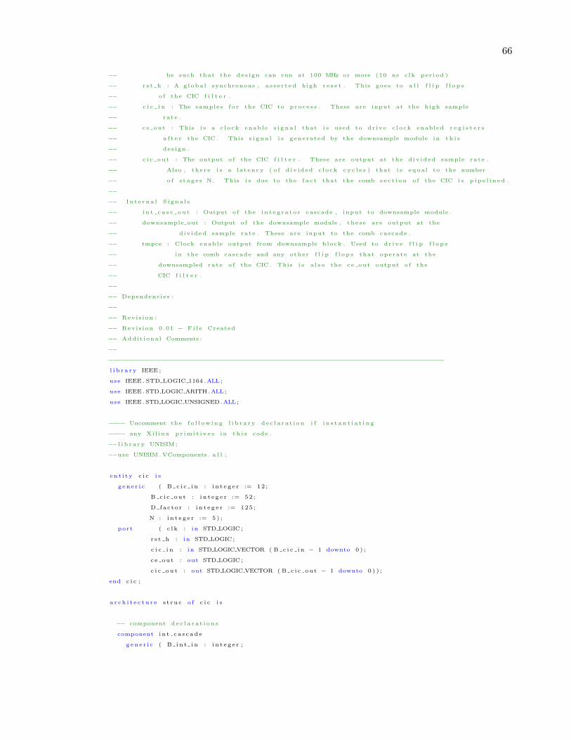
66
−− be such that the des ign can run at 100 MHz or more (10 ns c l k per iod )
−− r s t h : A g l oba l synchronous , a s s e r t ed high r e s e t . This goes to a l l f l i p f l o p s
−− o f the CIC f i l t e r .
−− c i c i n : The samples f o r the CIC to proce s s . These are input at the high sample
−− ra t e .
−− ce out : This i s a c l o ck enable s i g n a l that i s used to dr ive c l ock enabled r e g i s t e r s
−− a f t e r the CIC . This s i g n a l i s generated by the downsample module in t h i s
−− des ign .
−− c i c ou t : The output o f the CIC f i l t e r . These are output at the d iv ided sample ra t e .
−− Also , the re i s a l a t ency ( o f d iv ided c lock c y c l e s ) that i s equal to the number
−− o f s t age s N. This i s due to the f a c t that the comb s e c t i on o f the CIC i s p i p e l i n ed .
−−
−− I n t e r na l S i gna l s
−− i n t c a s c o u t : Output o f the i n t e g r a t o r cascade , input to downsample module .
−− downsample out : Output o f the downsample module , these are output at the
−− div ided sample ra t e . These are input to the comb cascade .
−− tmpce : Clock enable output from downsample block . Used to dr ive f l i p f l o p s
−− in the comb cascade and any other f l i p f l o p s that operate at the
−− downsampled ra t e o f the CIC . This i s a l s o the ce out output o f the
−− CIC f i l t e r .
−−
−− Dependencies :
−−
−− Revis ion :
−− Revis ion 0 .01 − F i l e Created
−− Addit iona l Comments :
−−
−−−−−−−−−−−−−−−−−−−−−−−−−−−−−−−−−−−−−−−−−−−−−−−−−−−−−−−−−−−−−−−−−−−−−−−−−−−−−−−−−−
l i b r a r y IEEE ;
use IEEE . STD LOGIC 1164 .ALL;
use IEEE .STD LOGIC ARITH.ALL;
use IEEE .STD LOGIC UNSIGNED.ALL;
−−−− Uncomment the f o l l ow ing l i b r a r y d e c l a r a t i on i f i n s t a n t i a t i n g
−−−− any Xi l inx p r im i t i v e s in t h i s code .
−−l i b r a r y UNISIM ;
−−use UNISIM . VComponents . a l l ;
e n t i t y c i c i s
g ene r i c ( B c i c i n : i n t e g e r := 12 ;
B c i c ou t : i n t e g e r := 52 ;
D factor : i n t e g e r := 125 ;
N : i n t e g e r := 5 ) ;
port ( c l k : in STD LOGIC;
r s t h : in STD LOGIC;
c i c i n : in STD LOGIC VECTOR ( B c i c i n − 1 downto 0 ) ;
c e out : out STD LOGIC;
c i c ou t : out STD LOGIC VECTOR ( B c i c ou t − 1 downto 0 ) ) ;
end c i c ;
a r c h i t e c t u r e s t ruc o f c i c i s
−− component d e c l a r a t i o n s
component i n t c a s c ade
g ene r i c ( B i n t i n : i n t e g e r ;

67
B int out : i n t e g e r ;
N : i n t e g e r ) ;
port ( c l k : in STD LOGIC;
r s t h : in STD LOGIC;
c a s c i n : in STD LOGIC VECTOR ( B in t i n − 1 downto 0 ) ;
ca s c out : out STD LOGIC VECTOR ( B int out − 1 downto 0 ) ) ;
end component i n t c a s c ade ;
component downsample
g ene r i c ( B downsample : i n t e g e r ;
D factor : i n t e g e r ;
N : i n t e g e r ) ;
port ( c l k : in STD LOGIC;
r s t h : in STD LOGIC;
data in : in STD LOGIC VECTOR (B downsample − 1 downto 0 ) ;
c l k en : out STD LOGIC;
data out : out STD LOGIC VECTOR (B downsample − 1 downto 0 ) ) ;
end component downsample ;
component comb cascade
g ene r i c ( B comb cascade : i n t e g e r ;
N : i n t e g e r ) ;
port ( c l k : in STD LOGIC;
r s t h : in STD LOGIC;
ce : in STD LOGIC;
c a s c i n : in STD LOGIC VECTOR ( B comb cascade − 1 downto 0 ) ;
ca s c out : out STD LOGIC VECTOR ( B comb cascade − 1 downto 0 ) ) ;
end component comb cascade ;
−− i n t e r n a l s i g n a l s
s i g n a l i n t c a s c o u t : STD LOGIC VECTOR( B c i c ou t − 1 downto 0 ) ; −− output o f i n t e g r a t o r s t age s
s i g n a l downsample out : STD LOGIC VECTOR( B c i c ou t − 1 downto 0 ) ; −− output o f downsample block
s i g n a l tmpce : STD LOGIC; −− ce output o f downsample block
begin −− arch . s t ruc o f c i c
−− i n s t a n t i a t e i n t e g r a t o r s t age s
i n t e g r a t o r s : i n t c a s c ade
g ene r i c map ( B in t i n => B c i c in , B int out => B cic out , N => N)
port map ( c lk => clk , r s t h => r s t h , c a s c i n => c i c i n , ca s c out => i n t c a s c o u t ) ;
−− i n s t a n t i a t e downsample block
decimator : downsample
g ene r i c map ( B downsample => B cic out , D factor => D factor , N => N)
port map ( c lk => clk , r s t h => r s t h , da ta in => i n t c a s c ou t , c l k en => tmpce ,
data out => downsample out ) ;
−− i n s t a n t i a t e comb s tage s
combs : comb cascade
g ene r i c map ( B comb cascade => B cic out , N => N)
port map ( c lk => clk , r s t h => r s t h , ce => tmpce , c a s c i n => downsample out ,
ca s c out => c i c o u t ) ;
−− a s s i gn the c l ock enable output to the i n t e r n a l s i g n a l tmpce
ce out ≤ tmpce ;

68
end s t ruc ;
−− c on f i gu r a t i on de c l a r a t i on f o r c i c en t i t y
c on f i gu r a t i on c i c c on o f c i c i s
f o r s t ruc
f o r i n t e g r a t o r s : i n t c a s c ade
use c on f i gu r a t i on work . i n t c a s cade con ;
end f o r ;
f o r decimator : downsample
use c on f i gu r a t i on work . downsample con ;
end f o r ;
f o r combs : comb cascade
use c on f i gu r a t i on work . comb cascade con ;
end f o r ;
end f o r ;
end con f i gu r a t i on c i c c on ;
quantizer.vhd
−−−−−−−−−−−−−−−−−−−−−−−−−−−−−−−−−−−−−−−−−−−−−−−−−−−−−−−−−−−−−−−−−−−−−−−−−−−−−−−−−−
−− Company :
−− Engineer :
−−
−− Create Date : 10 : 38 : 16 08/20/2007
−− Design Name :
−− Module Name : quant i z e r − behv
−− Pro j ec t Name :
−− Target Devices :
−− Tool v e r s i on s :
−− Desc r ip t i on : This VHDL ent i t y i s used to quant ize both the f u l l p r e c i s i o n CIC
−− f i l t e r output and the f u l l p r e c i s i o n polyphase FIR f i l t e r output . The
−− quant i za t i on method used here i s t runcat i on . Below are d e s c r i p t i o n s o f the
−− gene r i c s , ports , and i n t e r n a l s i g n a l s that are used in t h i s en t i t y .
−−
−− Gener ics
−− B in : The b i t width o f the input , e i t h e r the CIC output or the polyphase
−− FIR f i l t e r output .
−− B out : The b i t width o f the input a f t e r t runcat i on .
−−
−− Ports
−− inp : The f u l l p r e c i s i o n input .
−− outp : The quantized r ep r e s en ta t i on o f the input s i g n a l .
−−
−− I n t e r na l S i gna l s
−− There are no i n t e r n a l s i g n a l s in t h i s en t i t y .
−−
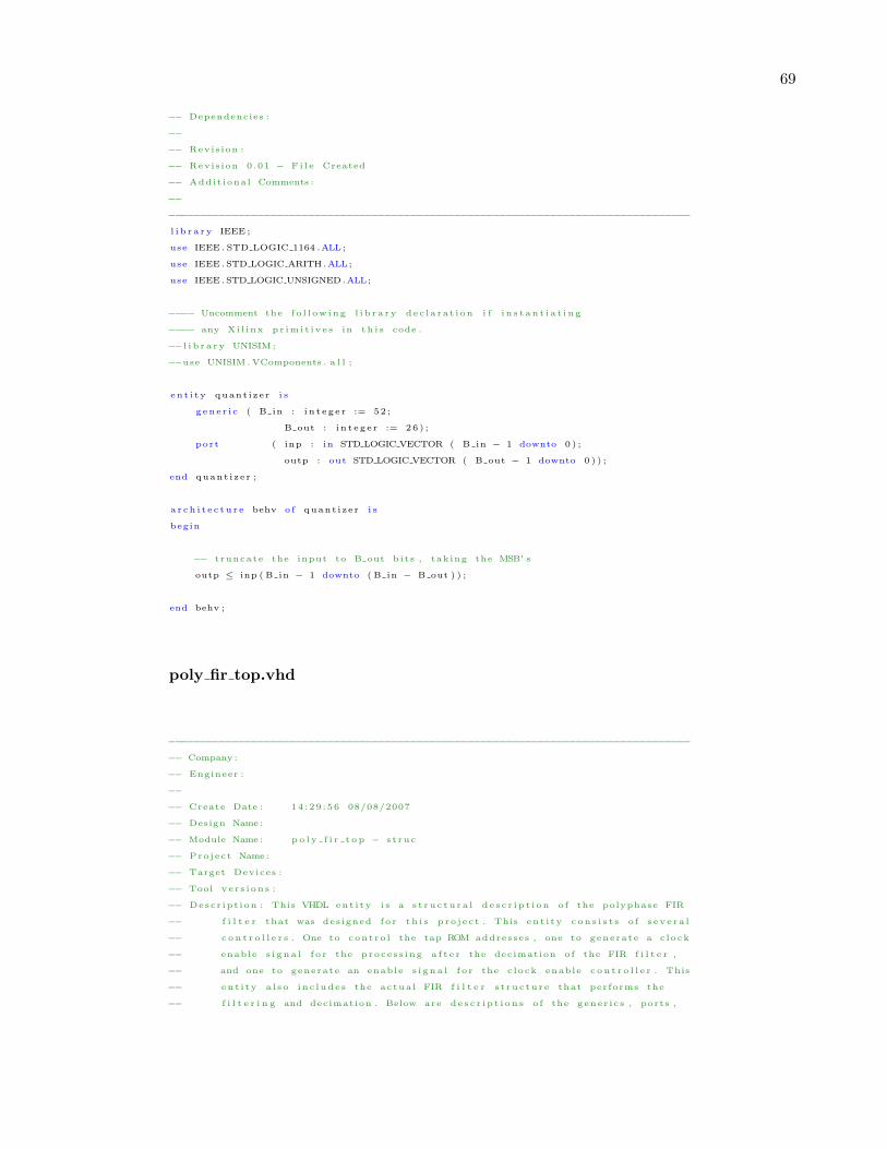
69
−− Dependencies :
−−
−− Revis ion :
−− Revis ion 0 .01 − F i l e Created
−− Addit iona l Comments :
−−
−−−−−−−−−−−−−−−−−−−−−−−−−−−−−−−−−−−−−−−−−−−−−−−−−−−−−−−−−−−−−−−−−−−−−−−−−−−−−−−−−−
l i b r a r y IEEE ;
use IEEE . STD LOGIC 1164 .ALL;
use IEEE .STD LOGIC ARITH.ALL;
use IEEE .STD LOGIC UNSIGNED.ALL;
−−−− Uncomment the f o l l ow ing l i b r a r y d e c l a r a t i on i f i n s t a n t i a t i n g
−−−− any Xi l inx p r im i t i v e s in t h i s code .
−−l i b r a r y UNISIM ;
−−use UNISIM . VComponents . a l l ;
e n t i t y quant i z e r i s
g ene r i c ( B in : i n t e g e r := 52 ;
B out : i n t e g e r := 26 ) ;
port ( inp : in STD LOGIC VECTOR ( B in − 1 downto 0 ) ;
outp : out STD LOGIC VECTOR ( B out − 1 downto 0 ) ) ;
end quant i z e r ;
a r c h i t e c t u r e behv o f quant i z e r i s
begin
−− t runcate the input to B out b i t s , tak ing the MSB' s
outp ≤ inp ( B in − 1 downto ( B in − B out ) ) ;
end behv ;
poly fir top.vhd
−−−−−−−−−−−−−−−−−−−−−−−−−−−−−−−−−−−−−−−−−−−−−−−−−−−−−−−−−−−−−−−−−−−−−−−−−−−−−−−−−−
−− Company :
−− Engineer :
−−
−− Create Date : 14 : 29 : 56 08/08/2007
−− Design Name :
−− Module Name : p o l y f i r t o p − s t ruc
−− Pro j ec t Name :
−− Target Devices :
−− Tool v e r s i on s :
−− Desc r ip t i on : This VHDL ent i t y i s a s t r u c t u r a l d e s c r i p t i o n o f the polyphase FIR
−− f i l t e r that was des igned f o r t h i s p r o j e c t . This en t i t y c o n s i s t s o f s e v e r a l
−− c o n t r o l l e r s . One to con t r o l the tap ROM addresses , one to generate a c l ock
−− enable s i g n a l f o r the p roc e s s i ng a f t e r the decimation o f the FIR f i l t e r ,
−− and one to generate an enable s i g n a l f o r the c l ock enable c o n t r o l l e r . This
−− en t i t y a l s o i n c l ude s the ac tua l FIR f i l t e r s t ru c tu r e that performs the
−− f i l t e r i n g and decimation . Below are d e s c r i p t i o n s o f the gene r i c s , ports ,

70
−− and i n t e r n a l s i g n a l s that t h i s en t i t y uses .
−−
−− Gener ics
−− N taps : The Number o f taps in the FIR f i l t e r .
−− N c i c s t a g e s : The Number o f s t age s in the preced ing CIC f i l t e r . This i s
−− needed to account f o r the la t ency inherent in the p i p e l i n ed
−− comb cascade in the CIC .
−− B coe f f s : The b i t width o f the f i l t e r c o e f f i c i e n t s used .
−− B input : The b i t width o f the input to the polyphase FIR f i l t e r .
−− B output : The f u l l p r e c i s i o n b i t width o f the output o f the polyphase FIR
−− f i l t e r .
−− D cic : The decimation f a c t o r o f the CIC f i l t e r .
−− D f i r : The decimation f a c t o r o f the polyphase FIR f i l t e r .
−− B rom addr : The number o f b i t s r equ i r ed f o r the address o f the tap ROMs.
−− This i s dependent on the g ene r i c D f i r , s i n c e the # of e lements
−− in each tap rom i s equal to D f i r . Thus t h i s g ene r i c can be
−− c a l cu l a t ed by the f o l l ow ing equat ion :
−−
−− B rom addr = c e i l ( log2 ( D f i r ) )
−−
−− Ports
−− c l k : The g l oba l c l o ck s i g n a l .
−− r s t h : The g loba l , synchronous , a s s e r t ed high r e s e t s i g n a l .
−− c e i n : The c l ock enable s i g n a l used f o r l o g i c that needs to operate at
−− the CIC output ra t e .
−− insample : The input samples , they are input to the polyphase FIR f i l t e r at
−− the CIC output ra t e .
−− ce out : The c l ock enable s i g n a l used f o r l o g i c that needs to operate at the
−− polyphase f i l t e r output ra t e .
−− outsample : The output o f the polyphase FIR f i l t e r . This i s f u l l p r e c i s i on ,
−− a lso , any l o g i c that p o t e n t i a l l y f o l l ow s t h i s output needs to
−− be dr iven by the c l ock enable s i g n a l ce out .
−−
−− I n t e r na l S i gna l s
−− tmp ce : The c l ock enable s i g n a l used to dr ive f l i p f l o p s that need to
−− operate at the polyphase FIR f i l t e r output ra t e . This i s a l s o
−− the ce out output o f t h i s en t i t y .
−− tmp en : The enable s i g n a l used to t e l l the c e c t r l e n t i t y when to s t a r t
−− counting c l ock s i g n a l s . This i s needed to account f o r the la t ency
−− o f the comb cascade o f the CIC f i l t e r .
−− addr : The address s i g n a l that i s generated by the add r c t r l e n t i t y . This
−− s i g n a l i s used to address data in the tap ROMs of the f i r t a p s
−− en t i t y .
−−
−− Dependencies :
−−
−− Revis ion :
−− Revis ion 0 .01 − F i l e Created
−− Addit iona l Comments :
−−
−−−−−−−−−−−−−−−−−−−−−−−−−−−−−−−−−−−−−−−−−−−−−−−−−−−−−−−−−−−−−−−−−−−−−−−−−−−−−−−−−−
l i b r a r y IEEE ;
use IEEE . STD LOGIC 1164 .ALL;
use IEEE .STD LOGIC ARITH.ALL;
use IEEE .STD LOGIC UNSIGNED.ALL;

71
−−−− Uncomment the f o l l ow ing l i b r a r y d e c l a r a t i on i f i n s t a n t i a t i n g
−−−− any Xi l inx p r im i t i v e s in t h i s code .
−−l i b r a r y UNISIM ;
−−use UNISIM . VComponents . a l l ;
e n t i t y p o l y f i r t o p i s
g ene r i c ( N taps : i n t e g e r := 30 ;
N c i c s t a g e s : i n t e g e r := 5 ;
B co e f f s : i n t e g e r := 14 ;
B input : i n t e g e r := 26 ;
B output : i n t e g e r := 48 ;
D cic : i n t e g e r := 10 ;
D f i r : i n t e g e r := 8 ;
B rom addr : i n t e g e r := 3 ) ;
Port ( c l k : in STD LOGIC;
r s t h : in STD LOGIC;
c e i n : in STD LOGIC;
insample : in STD LOGIC VECTOR ( B input − 1 downto 0 ) ;
c e out : out STD LOGIC;
outsample : out STD LOGIC VECTOR ( B output − 1 downto 0 ) ) ;
end p o l y f i r t o p ;
a r c h i t e c t u r e s t ruc o f p o l y f i r t o p i s
−− component d e c l a r a t i o n s
component c e c t r l
g ene r i c ( D cic : i n t e g e r ;
D f i r : i n t e g e r ) ;
port ( c l k : in STD LOGIC;
r s t h : in STD LOGIC;
en in : in STD LOGIC;
ce out : out STD LOGIC) ;
end component c e c t r l ;
component f i r t a p s
g ene r i c ( N taps : i n t e g e r ;
D factor : i n t e g e r ;
B co e f f s : i n t e g e r ;
B input : i n t e g e r ;
B output : i n t e g e r ;
B rom addr : i n t e g e r ) ;
port ( c l k : in STD LOGIC;
r s t h : in STD LOGIC;
c e f a s t : in STD LOGIC;
ce s l ow : in STD LOGIC;
f i r i n : in STD LOGIC VECTOR ( B input − 1 downto 0 ) ;
rom addr : in STD LOGIC VECTOR ( B rom addr − 1 downto 0 ) ;
f i r o u t : out STD LOGIC VECTOR ( B output − 1 downto 0 ) ) ;
end component f i r t a p s ;
component add r c t r l
g ene r i c ( B addr : i n t e g e r ) ;
port ( c l k : in STD LOGIC;
r s t h : in STD LOGIC;

72
en in : in STD LOGIC;
c e i n : in STD LOGIC;
addr out : out STD LOGIC VECTOR ( B addr − 1 downto 0 ) ) ;
end component add r c t r l ;
component e n c t r l
g ene r i c ( N c i c s t a g e s : i n t e g e r ) ;
port ( c l k : in STD LOGIC;
r s t h : in STD LOGIC;
c e i n : in STD LOGIC;
en out : out STD LOGIC) ;
end component e n c t r l ;
−− i n t e r n a l s i g n a l s
s i g n a l tmp ce : STD LOGIC;
s i g n a l addr : STD LOGIC VECTOR ( B rom addr − 1 downto 0 ) ;
s i g n a l tmp en : STD LOGIC;
begin
c t r l 0 : e n c t r l
g ene r i c map ( N c i c s t a g e s => N c i c s t a g e s )
port map ( c lk => clk , r s t h => r s t h , c e i n => ce in , en out => tmp en ) ;
c t r l 1 : c e c t r l
g ene r i c map ( D cic => D cic , D f i r => D f i r )
port map ( c lk => clk , r s t h => r s t h , en in => tmp en , ce out => tmp ce ) ;
c t r l 2 : a dd r c t r l
g ene r i c map ( B addr => B rom addr )
port map ( c lk => clk , en in => tmp en , c e i n => ce in , r s t h => r s t h , addr out => addr ) ;
f i r : f i r t a p s
g ene r i c map ( N taps => N taps , D factor => D f i r , B co e f f s => B coe f f s ,
B input => B input , B output => B output , B rom addr => B rom addr )
port map ( c lk => clk , r s t h => r s t h , c e f a s t => ce in , c e s l ow => tmp ce ,
f i r i n => insample , rom addr => addr , f i r o u t => outsample ) ;
c e out ≤ tmp ce ;
end s t ruc ;
c on f i gu r a t i on p o l y f i r t o p c o n o f p o l y f i r t o p i s
f o r s t ruc
f o r c t r l 1 : c e c t r l
use en t i t y work . c e c t r l ( behv ) ;
end f o r ;
f o r c t r l 2 : a dd r c t r l
use en t i t y work . a dd r c t r l ( behv ) ;
end f o r ;
f o r f i r : f i r t a p s
use c on f i gu r a t i on work . f i r t a p s c o n ;
end f o r ;

73
end f o r ;
end con f i gu r a t i on p o l y f i r t o p c o n ;
C.3 Third Level of the Hierarchy
int cascade.vhd
−−−−−−−−−−−−−−−−−−−−−−−−−−−−−−−−−−−−−−−−−−−−−−−−−−−−−−−−−−−−−−−−−−−−−−−−−−−−−−−−−−
−− Company :
−− Engineer :
−−
−− Create Date : 11 : 36 : 29 07/30/2007
−− Design Name :
−− Module Name : i n t c a s c ade − s t ruc
−− Pro j ec t Name :
−− Target Devices :
−− Tool v e r s i on s :
−− Desc r ip t i on : This VHDL ent i t y i s a s t r u c t u r a l d e s c r i p t i o n o f the i n t e g r a t o r
−− cascade o f the CIC f i l t e r . This en t i t y r e s i d e s in the second l e v e l o f the
−− h ie ra rchy o f the des ign . This cascade s i gn extends the input to the CIC
−− to the number o f b i t s on the output ( thus the accumulator b i t width ) and then
−− cascades N in t e g r a t o r s e c t i o n s toge the r . Below i s a d e s c r i p t i o n o f the g en e r i c s and
−− port s f o r t h i s en t i t y .
−−
−− Gener ics
−− B in t i n : # of b i t s on the input to the i n t e g r a t o r cascade , t h i s i s the
−− number o f b i t s on the input to the f i l t e r cascade .
−− B int out : # of b i t s on the output o f the i n t e g r a t o r cascade .
−− N : # of i n t e g r a t o r s t age s to cascade toge the r .
−−
−− Ports
−− c l k : Global c l o ck f o r e n t i r e CIC , the r e g i s t e r s in the i n t e g r a t o r s t age s
−− don ' t need to be c l ock enabled r e g i s t e r s because they need to operate
−− at the same sample ra t e o f the ADC.
−− r s t h : Global synchronous , a s s e r t ed high r e s e t s i g n a l .
−− c a s c i n : Input to the i n t e g r a t o r cascade .
−− ca s c out : Output o f the i n t e g r a t o r cascade .
−−
−− I n t e r na l S i gna l s
−− i n t r n s i g : This i s an array o f standard l o g i c v ec to r s that are equal in
−− l ength to the accumulator b i t width . Each row of the array i s
−− used as an output o f an i n t e g r a t o r s tage .
−− s gn ex t i n : This s i g n a l i s the input to the cascade s i gn extended to the
−− accumulator b i t width .
−−
−− Dependencies :
−−
−− Revis ion :
−− Revis ion 0 .01 − F i l e Created
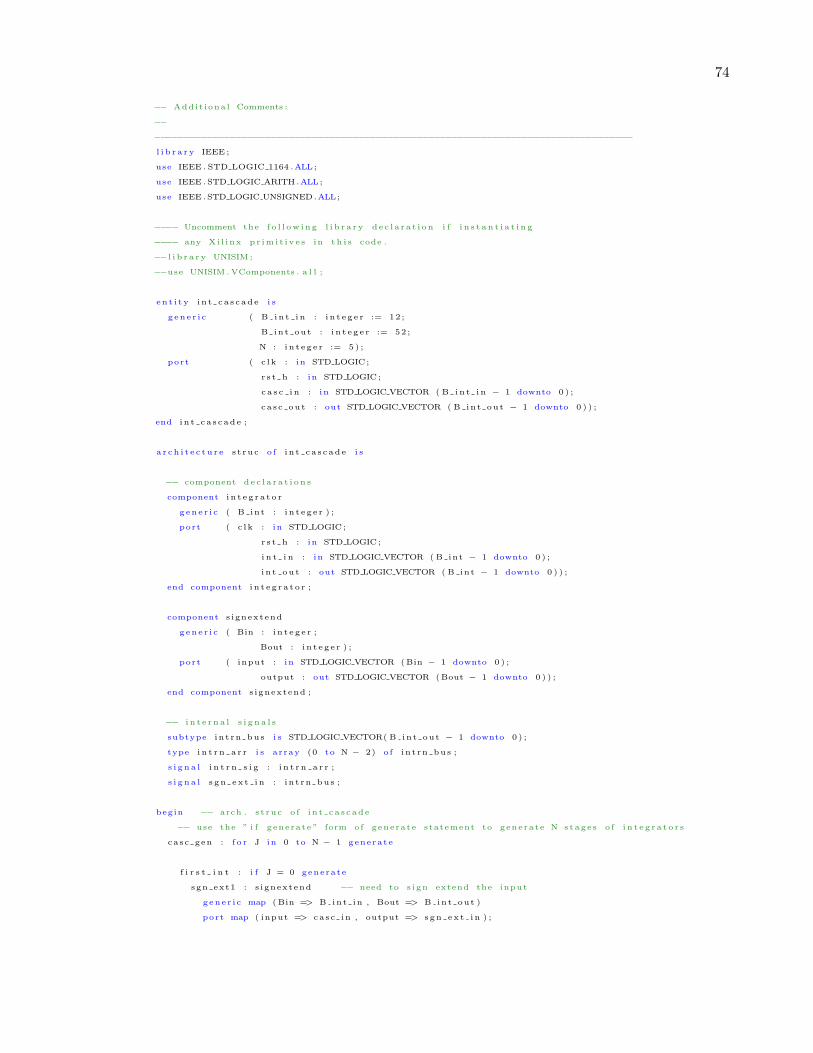
74
−− Addit iona l Comments :
−−
−−−−−−−−−−−−−−−−−−−−−−−−−−−−−−−−−−−−−−−−−−−−−−−−−−−−−−−−−−−−−−−−−−−−−−−−−−−−−−−−−−
l i b r a r y IEEE ;
use IEEE . STD LOGIC 1164 .ALL;
use IEEE .STD LOGIC ARITH.ALL;
use IEEE .STD LOGIC UNSIGNED.ALL;
−−−− Uncomment the f o l l ow ing l i b r a r y d e c l a r a t i on i f i n s t a n t i a t i n g
−−−− any Xi l inx p r im i t i v e s in t h i s code .
−−l i b r a r y UNISIM ;
−−use UNISIM . VComponents . a l l ;
e n t i t y i n t c a s c ade i s
g ene r i c ( B i n t i n : i n t e g e r := 12 ;
B int out : i n t e g e r := 52 ;
N : i n t e g e r := 5 ) ;
port ( c l k : in STD LOGIC;
r s t h : in STD LOGIC;
c a s c i n : in STD LOGIC VECTOR ( B in t i n − 1 downto 0 ) ;
ca s c out : out STD LOGIC VECTOR ( B int out − 1 downto 0 ) ) ;
end in t c a s c ade ;
a r c h i t e c t u r e s t ruc o f i n t c a s c ade i s
−− component d e c l a r a t i o n s
component i n t e g r a t o r
g ene r i c ( B int : i n t e g e r ) ;
port ( c l k : in STD LOGIC;
r s t h : in STD LOGIC;
i n t i n : in STD LOGIC VECTOR ( B int − 1 downto 0 ) ;
i n t ou t : out STD LOGIC VECTOR ( B int − 1 downto 0 ) ) ;
end component i n t e g r a t o r ;
component s ignextend
gene r i c ( Bin : i n t e g e r ;
Bout : i n t e g e r ) ;
port ( input : in STD LOGIC VECTOR (Bin − 1 downto 0 ) ;
output : out STD LOGIC VECTOR (Bout − 1 downto 0 ) ) ;
end component s ignextend ;
−− i n t e r n a l s i g n a l s
subtype in t rn bus i s STD LOGIC VECTOR( B int out − 1 downto 0 ) ;
type i n t r n a r r i s array (0 to N − 2) o f i n t rn bus ;
s i g n a l i n t r n s i g : i n t r n a r r ;
s i g n a l s gn ex t i n : i n t rn bus ;
begin −− arch . s t ruc o f i n t c a s c ade
−− use the ” i f generate ” form of generate statement to generate N s tage s o f i n t e g r a t o r s
casc gen : f o r J in 0 to N − 1 generate
f i r s t i n t : i f J = 0 generate
sgn ext1 : s ignextend −− need to s i gn extend the input
g ene r i c map (Bin => B int in , Bout => B int out )
port map ( input => ca s c in , output => s gn ex t i n ) ;

75
i n t e g r a t o r 1 : i n t e g r a t o r −− i n s t a n t i a t e an i n t e g r a t o r to operate on s i gn extended input
g ene r i c map ( B int => B int out )
port map ( c lk => clk , r s t h => r s t h , i n t i n => s gn ex t in , i n t ou t => i n t r n s i g ( J ) ) ;
end generate f i r s t i n t ;
mid int s : i f J > 0 and J < N − 1 generate
int s mid : i n t e g r a t o r −− cascade i n t e g r a t o r s toge the r
g ene r i c map ( B int => B int out )
port map ( c lk => clk , r s t h => r s t h , i n t i n => i n t r n s i g ( J − 1) , i n t ou t => i n t r n s i g ( J ) ) ;
end generate mid int s ;
l a s t i n t : i f J = N − 1 generate
i n t l a s t : i n t e g r a t o r −− a s s i gn output o f l a s t i n t e g r a t o r to output o f b lock
gene r i c map ( B int => B int out )
port map ( c lk => clk , r s t h => r s t h , i n t i n => i n t r n s i g ( J − 1) , i n t ou t => ca s c out ) ;
end generate l a s t i n t ;
end generate casc gen ;
end s t ruc ;
−− c on f i gu r a t i on de c l a r a t i on f o r i n t c a s c ade en t i t y
c on f i gu r a t i on in t ca s cade con o f i n t c a s c ade i s
f o r s t ruc
f o r casc gen (0)
f o r f i r s t i n t
f o r sgn ext1 : s ignextend
use en t i t y work . s ignextend ( behv ) ;
end f o r ;
f o r i n t e g r a t o r 1 : i n t e g r a t o r
use c on f i gu r a t i on work . i n t e g r a t o r c on ;
end f o r ;
end f o r ;
end f o r ;
f o r casc gen (1 to N − 2)
f o r mid int s
f o r in t s mid : i n t e g r a t o r
use c on f i gu r a t i on work . i n t e g r a t o r c on ;
end f o r ;
end f o r ;
end f o r ;
f o r casc gen (N − 1)
f o r l a s t i n t
f o r i n t l a s t : i n t e g r a t o r
use c on f i gu r a t i on work . i n t e g r a t o r c on ;
end f o r ;
end f o r ;
end f o r ;
end f o r ;
end con f i gu r a t i on i n t ca s cade con ;

76
downsample.vhd
−−−−−−−−−−−−−−−−−−−−−−−−−−−−−−−−−−−−−−−−−−−−−−−−−−−−−−−−−−−−−−−−−−−−−−−−−−−−−−−−−−
−− Company :
−− Engineer :
−−
−− Create Date : 13 : 37 : 51 08/02/2007
−− Design Name :
−− Module Name : downsample − s t ruc
−− Pro j ec t Name :
−− Target Devices :
−− Tool v e r s i on s :
−− Desc r ip t i on : This VHDL ent i t y i s a s t r u c t u r a l d e s c r i p t i o n o f the downsample block .
−− The downsample block c o n s i s t s o f two c o n t r o l l e r s / counters . The f i r s t c o n t r o l l e r
−− ( s t a r t c t r l ) that i s used i s needed to grab the c o r r e c t sample from the i n t e g r a t o r
−− cascade upon a r e s e t . S ince there are mul t ip l e i n t e g r a t o r stages , the f i r s t sample
−− that the downsampler needs to keep i s not the f i r s t sample that comes in a f t e r a r e s e t .
−− S t a r t c t r l s imply counts the number o f c y c l e s equ iva l en t to the number o f i n t e g r a t o r s t age s
−− o f the incoming c l ock and then outputs an enable s i g n a l to the c l k c t r l b lock .
−− The second c o n t r o l l e r in the downsample block i s the c l k c t r l b lock . This
−− block counts the number o f samples equ iva l en t to D factor and outputs a c l ock enable
−− s i g n a l to enable the r e g i s t e r s a f t e r the downsampler when the counter wraps to zero .
−− With these two c on t r o l l e r s , downsampling can be achieved by simply r e g i s t e r i n g the
−− input to the downsampler block with a c l ock enabled r e g i s t e r that i s dr iven by the
−− enable output o f the c l k c t r l c o n t r o l l e r . Below i s a d e s c r i p t i o n o f the gene r i c s ,
−− ports , and i n t e r n a l s i g n a l s o f the downsample block .
−−
−− Gener ics
−− B downsample : # of b i t s on input and output o f downsample block .
−− D factor : Factor that downsample block i s to decimate by .
−− N : # of s t age s in i n t e g r a t o r and comb cascade .
−−
−− Ports
−− c l k : Global c lock , used to generate c l ock enable s i g n a l based on D factor .
−− r s t h : Global synchronous , a s s e r t ed high r e s e t s i g n a l .
−− data in : Data coming from in t e g r a t o r stages , only every D factor−th sample i s
−− passed on to the comb s tage s .
−− c l k en : c l o ck enable output to dr ive comb cascade r e g i s t e r s . These r e g i s t e r s
−− operate at the incoming c l ock ra t e d iv ided by D factor .
−− data out : Data output from the downsample block . This i s s imply every D factor−th
−− input sample .
−−
−− I n t e r na l S i gna l s
−− fsm en : Output o f s t a r t c t r l , t h i s s i g n a l t e l l s the c l k c t r l module when to
−− s t a r t counting c y c l e s o f the fa s t , g l oba l c l o ck .
−− tmp en : Output o f the c l k c t r l module . This i s the c l k en output o f the
−− downsample block .
−−
−− Dependencies :
−−
−− Revis ion :
−− Revis ion 0 .01 − F i l e Created
−− Addit iona l Comments :

77
−−
−−−−−−−−−−−−−−−−−−−−−−−−−−−−−−−−−−−−−−−−−−−−−−−−−−−−−−−−−−−−−−−−−−−−−−−−−−−−−−−−−−
l i b r a r y IEEE ;
use IEEE . STD LOGIC 1164 .ALL;
use IEEE .STD LOGIC ARITH.ALL;
use IEEE .STD LOGIC UNSIGNED.ALL;
−−−− Uncomment the f o l l ow ing l i b r a r y d e c l a r a t i on i f i n s t a n t i a t i n g
−−−− any Xi l inx p r im i t i v e s in t h i s code .
−−l i b r a r y UNISIM ;
−−use UNISIM . VComponents . a l l ;
e n t i t y downsample i s
g ene r i c ( B downsample : i n t e g e r := 52 ;
D factor : i n t e g e r := 125 ;
N : i n t e g e r := 5 ) ;
port ( c l k : in STD LOGIC;
r s t h : in STD LOGIC;
data in : in STD LOGIC VECTOR (B downsample − 1 downto 0 ) ;
c l k en : out STD LOGIC;
data out : out STD LOGIC VECTOR (B downsample − 1 downto 0 ) ) ;
end downsample ;
a r c h i t e c t u r e s t ruc o f downsample i s
−− component d e c l a r a t i o n s
component c l k c t r l
g ene r i c ( D : i n t e g e r ) ;
port ( c l k : in STD LOGIC;
r s t h : in STD LOGIC;
en in : in STD LOGIC;
en out : out STD LOGIC) ;
end component c l k c t r l ;
component s t a r t c t r l
g ene r i c ( N : i n t e g e r ) ;
port ( c l k : in STD LOGIC;
r s t h : in STD LOGIC;
en : out STD LOGIC) ;
end component s t a r t c t r l ;
component c e r e g
g ene r i c ( B ce reg : i n t e g e r ) ;
port ( c l k : in STD LOGIC;
r s t h : in STD LOGIC;
ce : in STD LOGIC;
inp : in STD LOGIC VECTOR ( B ce reg − 1 downto 0 ) ;
outp : out STD LOGIC VECTOR ( B ce reg − 1 downto 0 ) ) ;
end component c e r e g ;
−− i n t e r n a l s i g n a l s
s i g n a l fsm en : STD LOGIC; −− enable s i g n a l f o r the c l ock enable s t a t e machine
s i g n a l tmp en : STD LOGIC; −− c l ock enable output f o r d iv ided c l ock
begin

78
−− i n s t a n t i a t e a s tar tup counter to enable c l o ck d i v i d e r s t a t e machine
s t a r t c n t : s t a r t c t r l
g ene r i c map (N => N)
port map ( c lk => clk , r s t h => r s t h , en => fsm en ) ;
−− i n s t a n t i a t e an enabled c l ock d i v i d e r s t a t e machine . This module outputs
−− the c l ock enable s i g n a l f o r a l l r e g i s t e r s in the comb cascade .
dsampler : c l k c t r l
g ene r i c map (D => D factor )
port map ( c lk => clk , r s t h => r s t h , en in => fsm en , en out => tmp en ) ;
−− r e g i s t e r the output o f the downsample block with a c l ock enabled r e g i s t e r ,
−− e f f e c t i v e l y downsampling the s i g n a l by D factor
outreg : c e r e g
g ene r i c map ( B ce reg => B downsample )
port map ( c lk => clk , r s t h => r s t h , ce => tmp en , inp => data in , outp => data out ) ;
−− a s s i gn output c l ock enable s i g n a l to i n t e r n a l s i g n a l tmp en
c l k en ≤ tmp en ;
end s t ruc ;
−− c on f i gu r a t i on de c l a r a t i on f o r downsample en t i t y
c on f i gu r a t i on downsample con o f downsample i s
f o r s t ruc
f o r s t a r t c n t : s t a r t c t r l
use en t i t y work . s t a r t c t r l ( behv ) ;
end f o r ;
f o r dsampler : c l k c t r l
use en t i t y work . c l k c t r l ( behv ) ;
end f o r ;
f o r outreg : c e r e g
use en t i t y work . c e r e g ( behv ) ;
end f o r ;
end f o r ;
end con f i gu r a t i on downsample con ;
comb cascade.vhd
−−−−−−−−−−−−−−−−−−−−−−−−−−−−−−−−−−−−−−−−−−−−−−−−−−−−−−−−−−−−−−−−−−−−−−−−−−−−−−−−−−
−− Company :
−− Engineer :
−−
−− Create Date : 07 : 11 : 28 08/03/2007
−− Design Name :
−− Module Name : comb cascade − s t ruc
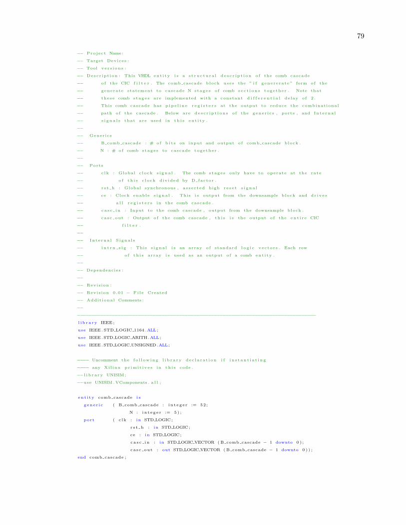
79
−− Pro j ec t Name :
−− Target Devices :
−− Tool v e r s i on s :
−− Desc r ip t i on : This VHDL ent i t y i s a s t r u c t u r a l d e s c r i p t i o n o f the comb cascade
−− o f the CIC f i l t e r . The comb cascade block uses the ” i f g ene r e ra t e ” form of the
−− generate statement to cascade N s tage s o f comb s e c t i o n s toge the r . Note that
−− these comb s tage s are implemented with a constant d i f f e r e n t i a l de lay o f 2 .
−− This comb cascade has p i p e l i n e r e g i s t e r s at the output to reduce the combinat ional
−− path o f the cascade . Below are d e s c r i p t i o n s o f the gene r i c s , ports , and In t e rna l
−− s i g n a l s that are used in t h i s en t i t y .
−−
−− Gener ics
−− B comb cascade : # of b i t s on input and output o f comb cascade block .
−− N : # of comb s tage s to cascade toge the r .
−−
−− Ports
−− c l k : Global c l o ck s i g n a l . The comb s tage s only have to operate at the ra t e
−− o f t h i s c l o ck d iv ided by D factor .
−− r s t h : Global synchronous , a s s e r t ed high r e s e t s i g n a l
−− ce : Clock enable s i g n a l . This i s output from the downsample block and d r i v e s
−− a l l r e g i s t e r s in the comb cascade .
−− c a s c i n : Input to the comb cascade , output from the downsample block .
−− ca s c out : Output o f the comb cascade , t h i s i s the output o f the e n t i r e CIC
−− f i l t e r .
−−
−− I n t e r na l S i gna l s
−− i n t r n s i g : This s i g n a l i s an array o f standard l o g i c ve c to r s . Each row
−− o f t h i s array i s used as an output o f a comb en t i t y .
−−
−− Dependencies :
−−
−− Revis ion :
−− Revis ion 0 .01 − F i l e Created
−− Addit iona l Comments :
−−
−−−−−−−−−−−−−−−−−−−−−−−−−−−−−−−−−−−−−−−−−−−−−−−−−−−−−−−−−−−−−−−−−−−−−−−−−−−−−−−−−−
l i b r a r y IEEE ;
use IEEE . STD LOGIC 1164 .ALL;
use IEEE .STD LOGIC ARITH.ALL;
use IEEE .STD LOGIC UNSIGNED.ALL;
−−−− Uncomment the f o l l ow ing l i b r a r y d e c l a r a t i on i f i n s t a n t i a t i n g
−−−− any Xi l inx p r im i t i v e s in t h i s code .
−−l i b r a r y UNISIM ;
−−use UNISIM . VComponents . a l l ;
e n t i t y comb cascade i s
g ene r i c ( B comb cascade : i n t e g e r := 52 ;
N : i n t e g e r := 5 ) ;
port ( c l k : in STD LOGIC;
r s t h : in STD LOGIC;
ce : in STD LOGIC;
c a s c i n : in STD LOGIC VECTOR ( B comb cascade − 1 downto 0 ) ;
ca s c out : out STD LOGIC VECTOR ( B comb cascade − 1 downto 0 ) ) ;
end comb cascade ;

80
a r ch i t e c t u r e s t ruc o f comb cascade i s
−− component d e c l a r a t i o n s
component comb
gene r i c ( B comb : i n t e g e r ) ;
port ( c l k : in STD LOGIC;
r s t h : in STD LOGIC;
ce : in STD LOGIC;
comb in : in STD LOGIC VECTOR (B comb − 1 downto 0 ) ;
comb out : out STD LOGIC VECTOR (B comb − 1 downto 0 ) ) ;
end component comb ;
−− i n t e r n a l s i g n a l s
subtype in t rn bus i s STD LOGIC VECTOR( B comb cascade − 1 downto 0 ) ;
type i n t r n a r r i s array (0 to N − 2) o f i n t rn bus ;
s i g n a l i n t r n s i g : i n t r n a r r ;
begin −− arch . s t ruc o f comb cascade
comb gen : f o r K in 0 to N − 1 generate
cmb1 : i f K = 0 generate
f i r s t cmb : comb
gene r i c map (B comb => B comb cascade )
port map ( c lk => clk , r s t h => r s t h , ce => ce ,
comb in => ca s c in , comb out => i n t r n s i g (K) ) ;
end generate cmb1 ;
mid cmbs : i f K > 0 and K < N − 1 generate
cmb mids : comb
gene r i c map (B comb => B comb cascade )
port map ( c lk => clk , r s t h => r s t h , ce => ce ,
comb in => i n t r n s i g (K − 1) , comb out => i n t r n s i g (K) ) ;
end generate mid cmbs ;
last cmb : i f K = N − 1 generate
cmb last : comb
gene r i c map (B comb => B comb cascade )
port map ( c lk => clk , r s t h => r s t h , ce => ce ,
comb in => i n t r n s i g (K − 1) , comb out => ca s c out ) ;
end generate last cmb ;
end generate comb gen ;
end s t ruc ;
−− c on f i gu r a t i on de c l a r a t i on f o r comb cascade en t i t y
c on f i gu r a t i on comb cascade con o f comb cascade i s
f o r s t ruc
f o r comb gen (0)
f o r cmb1
f o r f i r s t cmb : comb
use con f i gu r a t i on work . comb con ;

81
end f o r ;
end f o r ;
end f o r ;
f o r comb gen (1 to N − 1)
f o r mid cmbs
f o r cmb mids : comb
use con f i gu r a t i on work . comb con ;
end f o r ;
end f o r ;
end f o r ;
f o r comb gen (N − 1)
f o r last cmb
f o r cmb last : comb
use con f i gu r a t i on work . comb con ;
end f o r ;
end f o r ;
end f o r ;
end f o r ;
end con f i gu r a t i on comb cascade con ;
fir taps.vhd
−−−−−−−−−−−−−−−−−−−−−−−−−−−−−−−−−−−−−−−−−−−−−−−−−−−−−−−−−−−−−−−−−−−−−−−−−−−−−−−−−−
−− Company :
−− Engineer :
−−
−− Create Date : 14 : 36 : 40 08/08/2007
−− Design Name :
−− Module Name : f i r t a p s − s t ruc
−− Pro j ec t Name :
−− Target Devices :
−− Tool v e r s i on s :
−− Desc r ip t i on : This en t i t y i s a s t r u c t u r a l d e s c r i p t i o n o f a transposed d i r e c t
−− form FIR f i l t e r . To make t h i s a polyphase decimating f i l t e r , tap ROMs
−− conta in ing D factor c o e f f i c i e n t s are i n s e r t e d and the output o f the tap
−− mu l t i p l i e r s are accumulated f o r D factor c y c l e s . The c o e f f i c i e n t s are
−− s to r ed in the tap ROMs in such a way that f o r each cyc le , the equ iva l en t
−− FIR f i l t e r i s a polyphase r ep r e s en t a t i on o f the prototype f i l t e r . The
−− accumulators make i t so the f i l t e r outputs at a decimated ra t e . To s t o r e the
−− c o e f f i c i e n t s in the tap ROMs co r r e c t l y , a MATLAB s c r i p t ( p o l y f i l t .m) dea l s
−− the prototype f i l t e r c o e f f i c i e n t s out c o r r e c t l y and then wr i t e s these
−− c o e f f i c i e n t va lues to s e v e r a l t ext f i l e s that are then used to i n i t i a l i z e the
−− tap ROMs. Below are d e s c r i p t i o n s o f the gene r i c s , ports , and i n t e r n a l
−− i n t e r n a l s i g n a l s used in t h i s en t i t y .
−−
−− Gener ics
−− N taps : The number o f taps in the FIR f i l t e r .
−− D factor : The f a c t o r at which the f i l t e r w i l l decimate .

82
−− B coe f f s : The b i t width o f the c o e f f i c i e n t s s to r ed in the tap ROMs.
−− B input : The b i t width o f the input to the polyphase FIR f i l t e r .
−− B output : The b i t width o f the output o f the polyphase FIR f i l t e r . This
−− i s u sua l l y made to keep f u l l p r e c i s i o n through the mu l t i p l i e r s
−− and the accumulators . This i s a l s o the b i t width o f the
−− accumulators .
−− B rom addr : The number o f b i t s in the tap ROM address inputs .
−−
−− Ports
−− c l k : The g l oba l c l o ck s i g n a l .
−− r s t h : The g loba l , synchronous , a s s e r t ed high r e s e t s i g n a l
−− c e f a s t : The c l ock enable s i g n a l that d r i v e s f l i p f l o p s operat ing
−− at the CIC f i l t e r output ra t e .
−− ce s l ow : The c l ock enable s i g n a l that d r i v e s f l i p f l o p s operat ing
−− at the polyphase FIR f i l t e r output ra t e .
−− f i r i n : The input samples to the polyphase FIR f i l t e r .
−− rom addr : The address used to f e t ch data from the tap ROMs.
−− f i r o u t : The output o f the polyphase FIR f i l t e r . This i s u sua l l y kept
−− at f u l l p r e c i s i o n .
−−
−− I n t e r na l S i gna l s
−− i n t rn r om s i g : This s i g n a l i s an array o f standard l o g i c ve c to r s (SLVs) that
−− are used in the generate f o r loop as outputs o f the
−− tap ROMs. These are input to the tap mu l t i p l i e r s along with the
−− input s i gna l , f i r i n .
−− i n t r n mu l t s i g : This s i g n a l i s an array o f SLVs that are used in the generate
−− f o r loop as outputs o f the tap mu l t i p l i e r s . These are then
−− input to the accumulators .
−− i n t r n a c cD s i g : This s i g n a l i s an array o f SLVs that are used in the generate
−− f o r loop as outputs o f the accumulators . These are then input
−− to the tap adders along with the r e g i s t e r outputs from the
−− prev ious tap .
−− i n t r n r e g s i g : This s i g n a l i s an array o f SLVs used as outputs o f the tap
−− r e g i s t e r s used in the generate f o r loop . These are input
−− to the tap adders along with the accumulator outputs .
−− i n t r n add s i g : This s i g n a l i s an array o f SLVs used as outputs o f the
−− tap adders used in the generate f o r loop . These are then
−− input to the tap r e g i s t e r s .
−−
−− Dependencies :
−−
−− Revis ion :
−− Revis ion 0 .01 − F i l e Created
−− Addit iona l Comments :
−−
−−−−−−−−−−−−−−−−−−−−−−−−−−−−−−−−−−−−−−−−−−−−−−−−−−−−−−−−−−−−−−−−−−−−−−−−−−−−−−−−−−
l i b r a r y IEEE ;
use IEEE . STD LOGIC 1164 .ALL;
use IEEE .STD LOGIC ARITH.ALL;
use IEEE .STD LOGIC UNSIGNED.ALL;
−−−− Uncomment the f o l l ow ing l i b r a r y d e c l a r a t i on i f i n s t a n t i a t i n g
−−−− any Xi l inx p r im i t i v e s in t h i s code .
−−l i b r a r y UNISIM ;
−−use UNISIM . VComponents . a l l ;

83
en t i t y f i r t a p s i s
g ene r i c ( N taps : i n t e g e r := 30 ;
D factor : i n t e g e r := 8 ;
B co e f f s : i n t e g e r := 14 ;
B input : i n t e g e r := 26 ;
B output : i n t e g e r := 40 ;
B rom addr : i n t e g e r := 3 ) ;
port ( c l k : in STD LOGIC;
r s t h : in STD LOGIC;
c e f a s t : in STD LOGIC;
ce s l ow : in STD LOGIC;
f i r i n : in STD LOGIC VECTOR ( B input − 1 downto 0 ) ;
rom addr : in STD LOGIC VECTOR ( B rom addr − 1 downto 0 ) ;
f i r o u t : out STD LOGIC VECTOR ( B output − 1 downto 0 ) ) ;
end f i r t a p s ;
a r c h i t e c t u r e s t ruc o f f i r t a p s i s
−− component d e c l a r a t i o n s
component coe f f rom
gene r i c ( N elems : i n t e g e r := 8 ;
B data : i n t e g e r := 14 ;
B addr : i n t e g e r := 3 ;
fname : s t r i n g := ”rom0 . txt ” ) ;
port ( c l k : in STD LOGIC;
r s t h : in STD LOGIC;
en : in STD LOGIC;
addr : in STD LOGIC VECTOR ( B addr − 1 downto 0 ) ;
rom out : out STD LOGIC VECTOR ( B data − 1 downto 0 ) ) ;
end component coe f f rom ;
component gen mult
g ene r i c ( B mult in1 : i n t e g e r ;
B mult in2 : i n t e g e r ) ;
port ( in1 : in STD LOGIC VECTOR ( B mult in1 − 1 downto 0 ) ;
in2 : in STD LOGIC VECTOR ( B mult in2 − 1 downto 0 ) ;
prod : out STD LOGIC VECTOR (( B mult in1 + B mult in2 ) − 1 downto 0 ) ) ;
end component gen mult ;
component accum D
gene r i c ( D factor : i n t e g e r ;
B acc in : i n t e g e r ;
B acc out : i n t e g e r ) ;
port ( c l k : in STD LOGIC;
r s t h : in STD LOGIC;
c e i n : in STD LOGIC;
a c c i n : in STD LOGIC VECTOR ( B acc in − 1 downto 0 ) ;
acc out : out STD LOGIC VECTOR ( B acc out − 1 downto 0 ) ) ;
end component accum D ;
component c e r e g
g ene r i c ( B ce reg : i n t e g e r ) ;
port ( c l k : in STD LOGIC;
r s t h : in STD LOGIC;

84
ce : in STD LOGIC;
inp : in STD LOGIC VECTOR ( B ce reg − 1 downto 0 ) ;
outp : out STD LOGIC VECTOR ( B ce reg − 1 downto 0 ) ) ;
end component c e r e g ;
component gen adder
g ene r i c ( B adder : i n t e g e r ) ;
port ( add1 : in STD LOGIC VECTOR ( B adder − 1 downto 0 ) ;
add2 : in STD LOGIC VECTOR ( B adder − 1 downto 0 ) ;
sum : out STD LOGIC VECTOR ( B adder − 1 downto 0 ) ) ;
end component gen adder ;
−− i n t e r n a l s i g n a l s
subtype rom bus i s STD LOGIC VECTOR ( B co e f f s − 1 downto 0 ) ;
subtype mult out i s STD LOGIC VECTOR (( B co e f f s + B input ) − 1 downto 0 ) ;
subtype accD out i s STD LOGIC VECTOR ( B output − 1 downto 0 ) ;
type rom sig i s array (0 to N taps − 1) o f rom bus ;
type mu l t s i g i s array (0 to N taps − 1) o f mult out ;
type accD s ig i s array (0 to N taps − 1) o f accD out ;
type r e g s i g i s array (0 to N taps − 2) o f accD out ;
type add s ig i s array (1 to N taps − 1) o f accD out ;
s i g n a l i n t rn r om s i g : rom sig ;
s i g n a l i n t r n mu l t s i g : mu l t s i g ;
s i g n a l i n t r n a c cD s i g : accD s ig ;
s i g n a l i n t r n r e g s i g : r e g s i g ;
s i g n a l i n t r n add s i g : add s ig ;
begin −− arch . s t ruc o f f i r t a p s
tap gen : f o r J in 0 to N taps − 1 generate
begin
f i r s t t a p : i f J = 0 generate
begin
rom 0 : coe f f rom
gene r i c map ( N elems => D factor , B data => B coe f f s , B addr => B rom addr ,
fname => ( ”rom” & intege r ' image ( N taps − J − 1) & ” . txt ” ) )
port map ( c lk => clk , r s t h => r s t h , en => c e f a s t , addr => rom addr ,
rom out => i n t rn r om s i g ( J ) ) ;
mult 0 : gen mult
g ene r i c map ( B mult in1 => B input , B mult in2 => B coe f f s )
port map ( in1 => f i r i n , in2 => i n t rn r om s i g ( J ) , prod => i n t r n mu l t s i g ( J ) ) ;
accD 0 : accum D
gene r i c map ( D factor => D factor , B acc in => ( B co e f f s + B input ) ,
B acc out => B output )
port map ( c lk => clk , r s t h => r s t h , c e i n => c e f a s t ,
a c c i n => i n t r n mu l t s i g ( J ) , acc out => i n t r n a c cD s i g ( J ) ) ;
r eg 0 : c e r e g
g ene r i c map ( B ce reg => B output )
port map ( c lk => clk , r s t h => r s t h , ce => ce s low ,

85
inp => i n t r n a c cD s i g ( J ) , outp => i n t r n r e g s i g ( J ) ) ;
end generate f i r s t t a p ;
mid taps : i f J > 0 and J < N taps − 1 generate
begin
rom mid : coe f f rom
gene r i c map ( N elems => D factor , B data => B coe f f s , B addr => B rom addr ,
fname => ( ”rom” & intege r ' image ( N taps − J − 1) & ” . txt ” ) )
port map ( c lk => clk , r s t h => r s t h , en => c e f a s t , addr => rom addr ,
rom out => i n t rn r om s i g ( J ) ) ;
mult mid : gen mult
g ene r i c map ( B mult in1 => B input , B mult in2 => B coe f f s )
port map ( in1 => f i r i n , in2 => i n t rn r om s i g ( J ) , prod => i n t r n mu l t s i g ( J ) ) ;
accD mid : accum D
gene r i c map ( D factor => D factor , B acc in => ( B co e f f s + B input ) ,
B acc out => B output )
port map ( c lk => clk , r s t h => r s t h , c e i n => c e f a s t ,
a c c i n => i n t r n mu l t s i g ( J ) , acc out => i n t r n a c cD s i g ( J ) ) ;
add mid : gen adder
g ene r i c map ( B adder => B output )
port map ( add1 => i n t r n a c cD s i g ( J ) , add2 => i n t r n r e g s i g ( J − 1) ,
sum => i n t r n add s i g ( J ) ) ;
reg mid : c e r e g
g ene r i c map ( B ce reg => B output )
port map ( c lk => clk , r s t h => r s t h , ce => ce s low , inp => i n t r n add s i g ( J ) ,
outp => i n t r n r e g s i g ( J ) ) ;
end generate mid taps ;
l a s t t a p : i f J = N taps − 1 generate
begin
rom las t : coe f f rom
gene r i c map ( N elems => D factor , B data => B coe f f s , B addr => B rom addr ,
fname => ( ”rom” & intege r ' image ( N taps − J − 1) & ” . txt ” ) )
port map ( c lk => clk , r s t h => r s t h , en => c e f a s t , addr => rom addr ,
rom out => i n t rn r om s i g ( J ) ) ;
mu l t l a s t : gen mult
g ene r i c map ( B mult in1 => B input , B mult in2 => B coe f f s )
port map ( in1 => f i r i n , in2 => i n t rn r om s i g ( J ) , prod => i n t r n mu l t s i g ( J ) ) ;
a ccD la s t : accum D
gene r i c map ( D factor => D factor , B acc in => ( B co e f f s + B input ) ,
B acc out => B output )
port map ( c lk => clk , r s t h => r s t h , c e i n => c e f a s t ,
a c c i n => i n t r n mu l t s i g ( J ) , acc out => i n t r n a c cD s i g ( J ) ) ;
add l a s t : gen adder
g ene r i c map ( B adder => B output )
port map ( add1 => i n t r n a c cD s i g ( J ) , add2 => i n t r n r e g s i g ( J − 1) ,
sum => i n t r n add s i g ( J ) ) ;

86
r e g l a s t : c e r e g
g ene r i c map ( B ce reg => B output )
port map ( c lk => clk , r s t h => r s t h , ce => ce s low , inp => i n t r n add s i g ( J ) ,
outp => f i r o u t ) ;
end generate l a s t t a p ;
end generate tap gen ;
end s t ruc ;
c on f i gu r a t i on f i r t a p s c o n o f f i r t a p s i s
f o r s t ruc
f o r tap gen (0)
f o r f i r s t t a p
f o r rom 0 : coe f f rom
use en t i t y work . coe f f rom ( behv ) ;
end f o r ;
f o r mult 0 : gen mult
use en t i t y work . gen mult ( behv ) ;
end f o r ;
f o r accD 0 : accum D
use en t i t y work . accum D( behv ) ;
end f o r ;
f o r r eg 0 : c e r e g
use en t i t y work . c e r e g ( behv ) ;
end f o r ;
end f o r ;
end f o r ;
f o r tap gen (1 to N taps − 2)
f o r mid taps
f o r rom mid : coe f f rom
use en t i t y work . coe f f rom ( behv ) ;
end f o r ;
f o r mult mid : gen mult
use en t i t y work . gen mult ( behv ) ;
end f o r ;
f o r accD mid : accum D
use en t i t y work . accum D( behv ) ;
end f o r ;
f o r add mid : gen adder
use en t i t y work . gen adder ( behv ) ;
end f o r ;
f o r reg mid : c e r e g
use en t i t y work . c e r e g ( behv ) ;
end f o r ;
end f o r ;

87
end f o r ;
f o r tap gen ( N taps − 1)
f o r l a s t t a p
f o r rom las t : coe f f rom
use en t i t y work . coe f f rom ( behv ) ;
end f o r ;
f o r mu l t l a s t : gen mult
use en t i t y work . gen mult ( behv ) ;
end f o r ;
f o r accD la s t : accum D
use en t i t y work . accum D( behv ) ;
end f o r ;
f o r add l a s t : gen adder
use en t i t y work . gen adder ( behv ) ;
end f o r ;
f o r r e g l a s t : c e r e g
use en t i t y work . c e r e g ( behv ) ;
end f o r ;
end f o r ;
end f o r ;
end f o r ;
end con f i gu r a t i on f i r t a p s c o n ;
C.4 Fourth Level of the Hierarchy
integrator.vhd
−−−−−−−−−−−−−−−−−−−−−−−−−−−−−−−−−−−−−−−−−−−−−−−−−−−−−−−−−−−−−−−−−−−−−−−−−−−−−−−−−−
−− Company :
−− Engineer :
−−
−− Create Date : 11 : 11 : 48 07/30/2007
−− Design Name :
−− Module Name : i n t e g r a t o r − s t ruc
−− Pro j ec t Name :
−− Target Devices :
−− Tool v e r s i on s :
−− Desc r ip t i on : This VHDL ent i t y i s a s t r u c t u r a l d e s c r i p t i o n o f a s i n g l e i n t e g r a t o r
−− s tage . The s t ru c tu r e o f t h i s en t i t y i s such that there i s only one adder between each
−− accumulator r e g i s t e r o f the cascade . This g r e a t l y i n c r e a s e s the des ign
−− performance . Below are d e s c r i p t i o n s o f the gene r i c s , ports , and i n t e r n a l s i g n a l s
−− o f t h i s b lock .
−−

88
−− Gener ics
−− B int : # of b i t s on input and output o f i n t e g r a t o r s tage .
−−
−− Ports
−− c l k : Global c l o ck s i g n a l .
−− r s t h : Global synchronous , a s s e r t ed high r e s e t s i g n a l .
−− i n t i n : Input to i n t e g r a t o r s tage .
−− i n t ou t : Output to i n t e g r a t o r s tage .
−−
−− I n t e r na l S i gna l s
−− r eg out : This i s the output o f the accumulator r e g i s t e r . This s i g n a l
−− i s the output o f the in t eg ra to r , but i t a l s o f e ed s back in to
−− the second input o f the adder .
−− add out : This i s the output o f the adder in the i n t e g r a t o r .
−−
−− Dependencies :
−−
−− Revis ion :
−− Revis ion 0 .01 − F i l e Created
−− Addit iona l Comments :
−−
−−−−−−−−−−−−−−−−−−−−−−−−−−−−−−−−−−−−−−−−−−−−−−−−−−−−−−−−−−−−−−−−−−−−−−−−−−−−−−−−−−
l i b r a r y IEEE ;
use IEEE . STD LOGIC 1164 .ALL;
use IEEE .STD LOGIC ARITH.ALL;
use IEEE .STD LOGIC UNSIGNED.ALL;
−−−− Uncomment the f o l l ow ing l i b r a r y d e c l a r a t i on i f i n s t a n t i a t i n g
−−−− any Xi l inx p r im i t i v e s in t h i s code .
−−l i b r a r y UNISIM ;
−−use UNISIM . VComponents . a l l ;
e n t i t y i n t e g r a t o r i s
g ene r i c ( B int : i n t e g e r := 52 ) ;
port ( c l k : in STD LOGIC;
r s t h : in STD LOGIC;
i n t i n : in STD LOGIC VECTOR ( B int − 1 downto 0 ) ;
i n t ou t : out STD LOGIC VECTOR ( B int − 1 downto 0 ) ) ;
end i n t e g r a t o r ;
a r c h i t e c t u r e s t ruc o f i n t e g r a t o r i s
−− component d e c l a r a t i o n s
component gen reg
g ene r i c ( B : i n t e g e r ) ;
port ( c l k : in STD LOGIC;
r s t h : in STD LOGIC;
inp : in STD LOGIC VECTOR (B − 1 downto 0 ) ;
outp : out STD LOGIC VECTOR (B − 1 downto 0 ) ) ;
end component gen reg ;
component gen adder
g ene r i c ( B adder : i n t e g e r ) ;
port ( add1 : in STD LOGIC VECTOR ( B adder − 1 downto 0 ) ;
add2 : in STD LOGIC VECTOR ( B adder − 1 downto 0 ) ;

89
sum : out STD LOGIC VECTOR ( B adder − 1 downto 0 ) ) ;
end component gen adder ;
−− i n t e r n a l s i g n a l s
s i g n a l r eg out : STD LOGIC VECTOR( B int − 1 downto 0 ) ;
s i g n a l add out : STD LOGIC VECTOR( B int − 1 downto 0 ) ;
begin −− arch . s t ruc o f i n t e g r a t o r
−− i n s t a n t i a t e adder to perform accumulation
adder : gen adder
g ene r i c map ( B adder => B int )
port map ( add1 => i n t i n , add2 => reg out , sum => add out ) ;
−− i n s t a n t i a t e accumulator r e g i s t e r
a c c r eg : gen reg
g ene r i c map (B => B int )
port map ( c lk => clk , r s t h => r s t h , inp => add out , outp => r eg out ) ;
−− a s s i gn output o f b lock to i n t e r n a l s i g n a l r eg out
i n t ou t ≤ r eg out ;
end s t ruc ;
−− c on f i gu r a t i on de c l a r a t i on o f i n t e g r a t o r en t i t y
c on f i gu r a t i on i n t e g r a t o r c on o f i n t e g r a t o r i s
f o r s t ruc
f o r adder : gen adder
use en t i t y work . gen adder ( behv ) ;
end f o r ;
f o r a c c r eg : gen reg
use en t i t y work . gen reg ( behv ) ;
end f o r ;
end f o r ;
end con f i gu r a t i on i n t e g r a t o r c on ;
comb.vhd
−−−−−−−−−−−−−−−−−−−−−−−−−−−−−−−−−−−−−−−−−−−−−−−−−−−−−−−−−−−−−−−−−−−−−−−−−−−−−−−−−−
−− Company :
−− Engineer :
−−
−− Create Date : 16 : 13 : 49 08/02/2007
−− Design Name :
−− Module Name : comb − s t ruc
−− Pro j ec t Name :
−− Target Devices :
−− Tool v e r s i on s :
−− Desc r ip t i on : This VHDL ent i t y i s a s t r u c t u r a l d e s c r i p t i o n o f a s i n g l e comb stage
−− o f the comb cascade o f the CIC f i l t e r . This en t i t y i s p i p e l i n ed with output
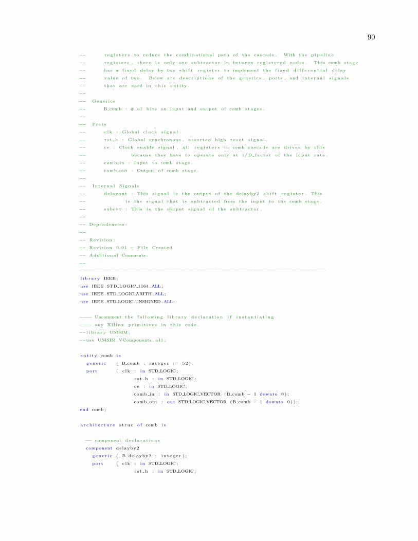
90
−− r e g i s t e r s to reduce the combinat ional path o f the cascade . With the p i p e l i n e
−− r e g i s t e r s , the re i s only one subt rac to r in between r e g i s t e r e d nodes . This comb stage
−− has a f i x ed delay by two s h i f t r e g i s t e r to implement the f i x ed d i f f e r e n t i a l de lay
−− value o f two . Below are d e s c r i p t i o n s o f the gene r i c s , ports , and i n t e r n a l s i g n a l s
−− that are used in t h i s en t i t y .
−−
−− Gener ics
−− B comb : # of b i t s on input and output o f comb s tage s .
−−
−− Ports
−− c l k : Global c l o ck s i g n a l .
−− r s t h : Global synchronous , a s s e r t ed high r e s e t s i g n a l .
−− ce : Clock enable s i gna l , a l l r e g i s t e r s in comb cascade are dr iven by t h i s
−− because they have to operate only at 1/ D factor o f the input ra t e .
−− comb in : Input to comb stage .
−− comb out : Output o f comb stage .
−−
−− I n t e r na l S i gna l s
−− delayout : This s i g n a l i s the output o f the delayby2 s h i f t r e g i s t e r . This
−− i s the s i g n a l that i s subtracted from the input to the comb stage .
−− subout : This i s the output s i g n a l o f the subt rac to r .
−−
−− Dependencies :
−−
−− Revis ion :
−− Revis ion 0 .01 − F i l e Created
−− Addit iona l Comments :
−−
−−−−−−−−−−−−−−−−−−−−−−−−−−−−−−−−−−−−−−−−−−−−−−−−−−−−−−−−−−−−−−−−−−−−−−−−−−−−−−−−−−
l i b r a r y IEEE ;
use IEEE . STD LOGIC 1164 .ALL;
use IEEE .STD LOGIC ARITH.ALL;
use IEEE .STD LOGIC UNSIGNED.ALL;
−−−− Uncomment the f o l l ow ing l i b r a r y d e c l a r a t i on i f i n s t a n t i a t i n g
−−−− any Xi l inx p r im i t i v e s in t h i s code .
−−l i b r a r y UNISIM ;
−−use UNISIM . VComponents . a l l ;
e n t i t y comb i s
g ene r i c ( B comb : i n t e g e r := 52 ) ;
port ( c l k : in STD LOGIC;
r s t h : in STD LOGIC;
ce : in STD LOGIC;
comb in : in STD LOGIC VECTOR (B comb − 1 downto 0 ) ;
comb out : out STD LOGIC VECTOR (B comb − 1 downto 0 ) ) ;
end comb ;
a r c h i t e c t u r e s t ruc o f comb i s
−− component d e c l a r a t i o n s
component delayby2
gene r i c ( B delayby2 : i n t e g e r ) ;
port ( c l k : in STD LOGIC;
r s t h : in STD LOGIC;

91
ce : in STD LOGIC;
d e l i n : in STD LOGIC VECTOR ( B delayby2 − 1 downto 0 ) ;
d e l ou t : out STD LOGIC VECTOR ( B delayby2 − 1 downto 0 ) ) ;
end component delayby2 ;
component gen subt rac to r
g ene r i c ( B subtractor : i n t e g e r ) ;
port ( sub1 : in STD LOGIC VECTOR ( B subtractor − 1 downto 0 ) ;
sub2 : in STD LOGIC VECTOR ( B subtractor − 1 downto 0 ) ;
d i f f : out STD LOGIC VECTOR ( B subtractor − 1 downto 0 ) ) ;
end component gen subt rac to r ;
component c e r e g
g ene r i c ( B ce reg : i n t e g e r := 52 ) ;
port ( c l k : in STD LOGIC;
r s t h : in STD LOGIC;
ce : in STD LOGIC;
inp : in STD LOGIC VECTOR ( B ce reg − 1 downto 0 ) ;
outp : out STD LOGIC VECTOR ( B ce reg − 1 downto 0 ) ) ;
end component c e r e g ;
−− i n t e r n a l s i g n a l s
s i g n a l de layout : STD LOGIC VECTOR(B comb − 1 downto 0 ) ; −− output o f de lay block
s i g n a l subout : STD LOGIC VECTOR(B comb − 1 downto 0 ) ; −− output o f subt rac to r block
begin −− arch . s t ruc o f comb
−− i n s t a n t i a t e a block to delay input s i g n a l by two samples
de lay : delayby2
gene r i c map ( B delayby2 => B comb)
port map ( c lk => clk , r s t h => r s t h , ce => ce , d e l i n => comb in , d e l ou t => delayout ) ;
subt rac to r : g en subt rac to r
g ene r i c map ( B subtractor => B comb)
port map ( sub1 => comb in , sub2 => delayout , d i f f => subout ) ;
−− r e g i s t e r the output to reduce the combinat ional path
outreg : c e r e g
g ene r i c map ( B ce reg => B comb)
port map ( c lk => clk , r s t h => r s t h , ce => ce , inp => subout , outp => comb out ) ;
end s t ruc ;
−− c on f i gu r a t i on de c l a r a t i on f o r comb en t i t y
c on f i gu r a t i on comb con o f comb i s
f o r s t ruc
f o r de lay : delayby2
use c on f i gu r a t i on work . delayby2 con ;
end f o r ;
f o r subt rac to r : g en subt rac to r
use en t i t y work . g en subt rac to r ( behv ) ;
end f o r ;

92
f o r outreg : c e r e g
use en t i t y work . c e r e g ( behv ) ;
end f o r ;
end f o r ;
end con f i gu r a t i on comb con ;
C.5 Fifth Level of the Hierarchy
delayby2.vhd
−−−−−−−−−−−−−−−−−−−−−−−−−−−−−−−−−−−−−−−−−−−−−−−−−−−−−−−−−−−−−−−−−−−−−−−−−−−−−−−−−−
−− Company :
−− Engineer :
−−
−− Create Date : 16 : 06 : 20 08/02/2007
−− Design Name :
−− Module Name : delayby2 − s t ruc
−− Pro j ec t Name :
−− Target Devices :
−− Tool v e r s i on s :
−− Desc r ip t i on : This en t i t y i s s imply a cascade o f two c lock enabled r e g i s t e r s
−− This en t i t y i s used to delay the input o f each comb stage by two samples
−− to implement the f i x ed d i f f e r e n t i a l de lay o f 2 that t h i s des ign uses .
−− Below are d e s c r i p t i o n s o f the gene r i c s , ports , and i n t e r n a l s i g n a l s that
−− are used in t h i s en t i t y .
−−
−− Gener ics
−− B delayby2 : # of b i t s in each r e g i s t e r o f t h i s en t i t y .
−−
−− Ports
−− c l k : A g l oba l c l o ck s i g n a l .
−− r s t h : A g l oba l syncronous , a s s e r t ed high r e s e t .
−− ce : The c l ock enable input that i s used to dr ive the r e g i s t e r s .
−− d e l i n : The input sample to the block .
−− de l ou t : The delayed input sample .
−−
−− I n t e r na l S i gna l s
−− delayby1 : This s i g n a l i s the output o f the f i r s t r e g i s t e r , input to the
−− second r e g i s t e r .
−−
−− Dependencies :
−−
−− Revis ion :
−− Revis ion 0 .01 − F i l e Created
−− Addit iona l Comments :
−−
−−−−−−−−−−−−−−−−−−−−−−−−−−−−−−−−−−−−−−−−−−−−−−−−−−−−−−−−−−−−−−−−−−−−−−−−−−−−−−−−−−
l i b r a r y IEEE ;

93
use IEEE . STD LOGIC 1164 .ALL;
use IEEE .STD LOGIC ARITH.ALL;
use IEEE .STD LOGIC UNSIGNED.ALL;
−−−− Uncomment the f o l l ow ing l i b r a r y d e c l a r a t i on i f i n s t a n t i a t i n g
−−−− any Xi l inx p r im i t i v e s in t h i s code .
−−l i b r a r y UNISIM ;
−−use UNISIM . VComponents . a l l ;
e n t i t y delayby2 i s
g ene r i c ( B delayby2 : i n t e g e r := 52 ) ;
port ( c l k : in STD LOGIC;
r s t h : in STD LOGIC;
ce : in STD LOGIC;
d e l i n : in STD LOGIC VECTOR ( B delayby2 − 1 downto 0 ) ;
d e l ou t : out STD LOGIC VECTOR ( B delayby2 − 1 downto 0 ) ) ;
end delayby2 ;
a r c h i t e c t u r e s t ruc o f delayby2 i s
−− component d e c l a r a t i o n s
component c e r e g
g ene r i c ( B ce reg : i n t e g e r ) ;
port ( c l k : in STD LOGIC;
r s t h : in STD LOGIC;
ce : in STD LOGIC;
inp : in STD LOGIC VECTOR ( B ce reg − 1 downto 0 ) ;
outp : out STD LOGIC VECTOR ( B ce reg − 1 downto 0 ) ) ;
end component c e r e g ;
−− i n t e r n a l s i g n a l s
s i g n a l delayby1 : STD LOGIC VECTOR( B delayby2 − 1 downto 0 ) ;
begin
−− c r ea t e a r e g i s t e r to de lay sample by one cyc l e
de layreg1 : c e r e g
g ene r i c map ( B ce reg => B delayby2 )
port map ( c lk => clk , r s t h => r s t h , ce => ce , inp => de l i n , outp => delayby1 ) ;
−− cascade a second r e g i s t e r to de lay sample by two cy c l e s
de layreg2 : c e r e g
g ene r i c map ( B ce reg => B delayby2 )
port map ( c lk => clk , r s t h => r s t h , ce => ce , inp => delayby1 , outp => de l ou t ) ;
end s t ruc ;
−− c on f i gu r a t i on de c l a r a t i on f o r delayby2 en t i t y
c on f i gu r a t i on delayby2 con o f delayby2 i s
f o r s t ruc
f o r a l l : c e r e g
use en t i t y work . c e r e g ( behv ) ;
end f o r ;
end f o r ;
end con f i gu r a t i on delayby2 con ;

94
C.6 Leaf Nodes
ce ctrl.vhd
−−−−−−−−−−−−−−−−−−−−−−−−−−−−−−−−−−−−−−−−−−−−−−−−−−−−−−−−−−−−−−−−−−−−−−−−−−−−−−−−−−
−− Company :
−− Engineer :
−−
−− Create Date : 18 : 07 : 41 08/07/2007
−− Design Name :
−− Module Name : c e c t r l − behv
−− Pro j ec t Name :
−− Target Devices :
−− Tool v e r s i on s :
−− Desc r ip t i on : This VHDL ent i t y i s used to generate the c l ock enable s i g n a l
−− that d r i v e s f l i p f l o p s operat ing at the polyphase FIR f i l t e r output ra t e .
−− This en t i t y uses the combined decimation f a c t o r ( D cic ∗ D f i r ) and the
−− g l oba l c l o ck in s t ead o f t ry ing to count the c l ock enable s i g n a l that i s
−− generated by the downsample en t i t y o f the CIC f i l t e r . This en t i t y has an
−− enable input to account f o r the la t ency due to the p i p e l i n ed s t ru c tu r e o f
−− the comb cascade o f the CIC f i l t e r . This en t i t y does not s t a r t counting
−− c l ock c y c l e s un t i l the enable s i g n a l i s a s s e r t ed .
−−
−− Gener ics
−− D cic : The decimation f a c t o r o f the CIC f i l t e r .
−− D f i r : The decimation f a c t o r o f the polyphase FIR f i l t e r .
−−
−− Ports
−− c l k : The g l oba l c l o ck s i g n a l
−− r s t h : The g loba l , synchronous , a s s e r t ed high r e s e t s i g n a l
−− en in : The a s s e r t ed high enable s i g n a l that t e l l s the en t i t y when to
−− s t a r t counting c l ock c y c l e s .
−− ce out : The c l ock enable s i g n a l that i s used to dr ive f l i p f l o p s that
−− operate at the polyphase FIR f i l t e r output ra t e .
−−
−− I n t e r na l S i gna l s
−− count : The counter s i g n a l that i s used to count g l oba l c l o ck c y c l e s . When
−− t h i s s i g n a l ge t s r e s e t to zero , the ce out output ge t s a s s e r t ed .
−−
−− Dependencies :
−−
−− Revis ion :
−− Revis ion 0 .01 − F i l e Created
−− Addit iona l Comments :
−−
−−−−−−−−−−−−−−−−−−−−−−−−−−−−−−−−−−−−−−−−−−−−−−−−−−−−−−−−−−−−−−−−−−−−−−−−−−−−−−−−−−
l i b r a r y IEEE ;
use IEEE . STD LOGIC 1164 .ALL;
use IEEE .STD LOGIC ARITH.ALL;
use IEEE .STD LOGIC UNSIGNED.ALL;

95
−−−− Uncomment the f o l l ow ing l i b r a r y d e c l a r a t i on i f i n s t a n t i a t i n g
−−−− any Xi l inx p r im i t i v e s in t h i s code .
−−l i b r a r y UNISIM ;
−−use UNISIM . VComponents . a l l ;
e n t i t y c e c t r l i s
g ene r i c ( D cic : i n t e g e r := 10 ;
D f i r : i n t e g e r := 8 ) ;
port ( c l k : in STD LOGIC;
r s t h : in STD LOGIC;
en in : in STD LOGIC;
ce out : out STD LOGIC) ;
end c e c t r l ;
a r c h i t e c t u r e behv o f c e c t r l i s
−− constant value determining combined decimation f a c t o r
constant D factor : i n t e g e r := ( D cic ∗ D f i r ) ;
−− i n t e r n a l s i g n a l used to count g l oba l c l o ck c y c l e s
s i g n a l count : i n t e g e r range 0 to D factor ;
begin
ce count : p roce s s ( c l k )
begin
i f c lk ' event and c lk = '1 ' then −− do everyth ing on posedge o f c l o ck
i f r s t h = '1 ' then −− c r ea t e a synchronous r e s e t
count ≤ 0 ;
ce out ≤ '0 ' ;
e l s i f en in = '1 ' then −− s t a r t counting when en in ge t s a s s e r t ed
i f count ≤ ( D factor − 1) then −− keep counting un t i l count = D factor −1
i f count = 0 then −− when count wraps to zero , a s s e r t ce out
ce out ≤ '1 ' ;
count ≤ count + 1 ;
e l s e −− keep counting un t i l count = D factor −1
ce out ≤ '0 ' ;
count ≤ count + 1 ;
end i f ; −− count = 0
e l s e
count ≤ 0 ;
ce out ≤ '0 ' ;
end i f ; −− count ≤ ( D factor −1)
end i f ; −− en in = '1 '
end i f ; −− clk ' event and c lk = '1 '
end proce s s ce count ;
end behv ;
addr ctrl.vhd
−−−−−−−−−−−−−−−−−−−−−−−−−−−−−−−−−−−−−−−−−−−−−−−−−−−−−−−−−−−−−−−−−−−−−−−−−−−−−−−−−−
−− Company :
−− Engineer :
−−
−− Create Date : 16 : 35 : 43 08/16/2007

96
−− Design Name :
−− Module Name : add r c t r l − behv
−− Pro j ec t Name :
−− Target Devices :
−− Tool v e r s i on s :
−− Desc r ip t i on : This VHDL ent i t y gene ra t e s the address used to f e t ch c o e f f i c i e n t
−− va lues out o f the tap ROMs in the f i r t a p s en t i t y . This generated address
−− goes to a l l o f the tap ROMs. As you can see , t h i s en t i t y i s s imply a down
−− counter that ge t s s e t to the maximum value when i t i s r e s e t . I t i s
−− important to note that t h i s en t i t y i s dr iven by an enable s i g n a l as we l l
−− as a c l ock enable s i g n a l . This en t i t y i s enabled f o r the same reason that
−− the c e c t r l en t i t y i s enabled , to account f o r the la t ency in the combs o f
−− the CIC f i l t e r . This en t i t y i s a l s o dr ive by a c l ock enable because i t needs
−− to operate at the CIC f i l t e r output ra t e .
−−
−− Gener ics
−− B addr : The number o f b i t s in the address o f the tap ROMs.
−−
−− Ports
−− c l k : The g l oba l c l o ck s i g n a l .
−− r s t h : The g loba l , synchronous , a s s e r t ed high r e s e t s i g n a l .
−− en in : An enable s i g n a l t e l l i n g the counter when to decrement . The counter
−− decrements when t h i s input and the c e i n input are both high .
−− c e i n : The c l ock enable s i g n a l that makes the counter decrement at the
−− CIC f i l t e r output ra t e .
−− adddr out : The generated address that i s used to f e t ch data from the
−− tap ROMs in the f i r t a p s en t i t y .
−−
−− I n t e r na l S i gna l s
−− count : A counter s i g n a l that decrements when t h i s en t i t y i s enabled and
−− at the CIC f i l t e r output ra t e . This i n t e r n a l s i g n a l i s a c tua l l y the
−− addr out output .
−−
−− Dependencies :
−−
−− Revis ion :
−− Revis ion 0 .01 − F i l e Created
−− Addit iona l Comments :
−−
−−−−−−−−−−−−−−−−−−−−−−−−−−−−−−−−−−−−−−−−−−−−−−−−−−−−−−−−−−−−−−−−−−−−−−−−−−−−−−−−−−
l i b r a r y IEEE ;
use IEEE . STD LOGIC 1164 .ALL;
use IEEE .STD LOGIC ARITH.ALL;
use IEEE .STD LOGIC UNSIGNED.ALL;
−−−− Uncomment the f o l l ow ing l i b r a r y d e c l a r a t i on i f i n s t a n t i a t i n g
−−−− any Xi l inx p r im i t i v e s in t h i s code .
−−l i b r a r y UNISIM ;
−−use UNISIM . VComponents . a l l ;
e n t i t y add r c t r l i s
g ene r i c ( B addr : i n t e g e r := 3 ) ;
port ( c l k : in STD LOGIC;
r s t h : in STD LOGIC;
en in : in STD LOGIC;

97
c e i n : in STD LOGIC;
addr out : out STD LOGIC VECTOR ( B addr − 1 downto 0 ) ) ;
end add r c t r l ;
a r c h i t e c t u r e behv o f a dd r c t r l i s
−− dec l a r e a counter s i g n a l used f o r address output
s i g n a l count : STD LOGIC VECTOR ( B addr − 1 downto 0 ) ;
begin
counter : p roce s s ( c l k )
begin
i f c lk ' event and c lk = '1 ' then −− do everyth ing on posedge o f c l o ck
i f r s t h = '1 ' then −− make a synchronous r e s e t
count ≤ ( o the r s => ' 1 ' ) ; −− s e t address to max . value on a r e s e t
e l s i f en in = '1 ' and c e i n = '1 ' then −− decrement when en in and c e i n are '1 '
count ≤ count − 1 ;
end i f ; −− en in = '1 ' and c e i n = '1 '
addr out ≤ count ; −− a s s i gn count to output
end i f ; −− clk ' event and c lk = '1 '
end proce s s counter ;
end behv ;
en ctrl.vhd
−−−−−−−−−−−−−−−−−−−−−−−−−−−−−−−−−−−−−−−−−−−−−−−−−−−−−−−−−−−−−−−−−−−−−−−−−−−−−−−−−−
−− Company :
−− Engineer :
−−
−− Create Date : 13 : 43 : 31 09/01/2007
−− Design Name :
−− Module Name : e n c t r l − behv
−− Pro j ec t Name :
−− Target Devices :
−− Tool v e r s i on s :
−− Desc r ip t i on : This VHDL ent i t y i s used to account f o r the la t ency o f the
−− comb cascade in the CIC f i l t e r . I t s imply counts the number o f c l o ck enable
−− s i g n a l s that are generated by the downsample en t i t y in the CIC f i l t e r and
−− outputs an enable s i g n a l based on the number o f comb s tage s that e x i s t . This
−− enable s i g n a l i s then used to t e l l the c e c t r l en t i t y when to s t a r t counting
−− c y c l e s o f the g l oba l c l o ck . Below are d e s c r i p t i o n s o f the gene r i c s , ports ,
−− and i n t e r n a l s i g n a l s that are used in t h i s en t i t y .
−−
−− Gener ics
−− N c i c s t ag e : The number o f s t age s in the CIC f i l t e r that precedes t h i s
−− polyphase FIR f i l t e r .
−−
−− Ports
−− c l k : The g l oba l c l o ck s i g n a l .
−− r s t h : A globa l , synchronous , a s s e r t ed high r e s e t s i g n a l .
−− c e i n : The c l ock enable s i g n a l generated in the downsample block o f the
−− CIC f i l t e r . This i s what ge t s counted .
−− en out : The enable output that t e l l s the c e c t r l module when to s t a r t
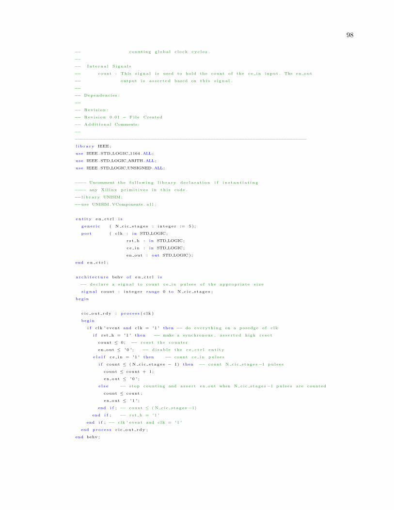
98
−− counting g l oba l c l o ck c y c l e s .
−−
−− I n t e r na l S i gna l s
−− count : This s i g n a l i s used to hold the count o f the c e i n input . The en out
−− output i s a s s e r t ed based on t h i s s i g n a l .
−−
−− Dependencies :
−−
−− Revis ion :
−− Revis ion 0 .01 − F i l e Created
−− Addit iona l Comments :
−−
−−−−−−−−−−−−−−−−−−−−−−−−−−−−−−−−−−−−−−−−−−−−−−−−−−−−−−−−−−−−−−−−−−−−−−−−−−−−−−−−−−
l i b r a r y IEEE ;
use IEEE . STD LOGIC 1164 .ALL;
use IEEE .STD LOGIC ARITH.ALL;
use IEEE .STD LOGIC UNSIGNED.ALL;
−−−− Uncomment the f o l l ow ing l i b r a r y d e c l a r a t i on i f i n s t a n t i a t i n g
−−−− any Xi l inx p r im i t i v e s in t h i s code .
−−l i b r a r y UNISIM ;
−−use UNISIM . VComponents . a l l ;
e n t i t y e n c t r l i s
g ene r i c ( N c i c s t a g e s : i n t e g e r := 5 ) ;
port ( c l k : in STD LOGIC;
r s t h : in STD LOGIC;
c e i n : in STD LOGIC;
en out : out STD LOGIC) ;
end e n c t r l ;
a r c h i t e c t u r e behv o f e n c t r l i s
−− dec l a r e a s i g n a l to count c e i n pu l s e s o f the appropr ia te s i z e
s i g n a l count : i n t e g e r range 0 to N c i c s t a g e s ;
begin
c i c ou t r dy : p roce s s ( c l k )
begin
i f c lk ' event and c lk = '1 ' then −− do everyth ing on a posedge o f c l k
i f r s t h = '1 ' then −− make a synchronous , a s s e r t ed high r e s e t
count ≤ 0 ; −− r e s e t the counter
en out ≤ '0 ' ; −− d i s ab l e the c e c t r l en t i t y
e l s i f c e i n = '1 ' then −− count c e i n pu l s e s
i f count ≤ ( N c i c s t a g e s − 1) then −− count N c i c s t age s −1 pu l s e s
count ≤ count + 1 ;
en out ≤ '0 ' ;
e l s e −− stop counting and a s s e r t en out when N c i c s t age s −1 pu l s e s are counted
count ≤ count ;
en out ≤ '1 ' ;
end i f ; −− count ≤ ( N c i c s t age s −1)
end i f ; −− r s t h = '1 '
end i f ; −− clk ' event and c lk = '1 '
end proce s s c i c ou t r dy ;
end behv ;

99
signextend.vhd
−−−−−−−−−−−−−−−−−−−−−−−−−−−−−−−−−−−−−−−−−−−−−−−−−−−−−−−−−−−−−−−−−−−−−−−−−−−−−−−−−−
−− Company :
−− Engineer :
−−
−− Create Date : 10 : 16 : 16 07/30/2007
−− Design Name :
−− Module Name : s ignextend − behv
−− Pro j ec t Name :
−− Target Devices :
−− Tool v e r s i on s :
−− Desc r ip t i on : This VHDL ent i t y i s a s imple s i gn extender . I t i s used to s i gn
−− extend the input o f the CIC to the accumulator b i t width o f the f i r s t
−− i n t e g r a t o r s tage . To do th i s , i t uses the ” f o r generate ” form of the generate
−− loop . Below are d e s c r i p t i o n s o f the gene r i c s , ports , and i n t e r n a l s i g n a l s that
−− are used in t h i s module .
−−
−− Gener ics
−− Bin : # of b i t s on the input port o f module .
−− Bout : # of b i t s on the output port o f module .
−−
−− Ports
−− input : Non−s i gn extended value from ADC.
−− output : Sign extended value from ADC.
−−
−− I n t e r na l S i gna l s
−− This module has no i n t e r n a l s i g n a l s .
−−
−− Dependencies :
−−
−− Revis ion :
−− Revis ion 0 .01 − F i l e Created
−− Addit iona l Comments :
−−
−−−−−−−−−−−−−−−−−−−−−−−−−−−−−−−−−−−−−−−−−−−−−−−−−−−−−−−−−−−−−−−−−−−−−−−−−−−−−−−−−−
l i b r a r y IEEE ;
use IEEE . STD LOGIC 1164 .ALL;
use IEEE .STD LOGIC ARITH.ALL;
use IEEE .STD LOGIC UNSIGNED.ALL;
−−−− Uncomment the f o l l ow ing l i b r a r y d e c l a r a t i on i f i n s t a n t i a t i n g
−−−− any Xi l inx p r im i t i v e s in t h i s code .
−−l i b r a r y UNISIM ;
−−use UNISIM . VComponents . a l l ;
e n t i t y s ignextend i s
g ene r i c ( Bin : i n t e g e r := 13 ;
Bout : i n t e g e r := 52 ) ;
port ( input : in STD LOGIC VECTOR (Bin − 1 downto 0 ) ;
output : out STD LOGIC VECTOR (Bout − 1 downto 0 ) ) ;
end s ignextend ;

100
a r ch i t e c t u r e behv o f s ignextend i s
begin
output ( Bin − 1 downto 0) ≤ input ;
sgn ext : f o r j in Bin to Bout − 1 generate
output ( j ) ≤ input ( Bin − 1 ) ;
end generate sgn ext ;
end behv ;
clk ctrl.vhd
−−−−−−−−−−−−−−−−−−−−−−−−−−−−−−−−−−−−−−−−−−−−−−−−−−−−−−−−−−−−−−−−−−−−−−−−−−−−−−−−−−
−− Company :
−− Engineer :
−−
−− Create Date : 11 : 48 : 33 08/02/2007
−− Design Name :
−− Module Name : c l k c t r l − behv
−− Pro j ec t Name :
−− Target Devices :
−− Tool v e r s i on s :
−− Desc r ip t i on : This VHDL ent i t y i s a l e a f node o f the downsample block . This en t i t y
−− c r e a t e s a c l ock enable s i g n a l based on the incoming , g l oba l c l o ck s i g n a l .
−− This c l o ck enable s i g n a l i s then used to dr ive c l ock enabled r e g i s t e r s l a t e r
−− on in the p roc e s s i ng chain . C l k c t r l counts a c e r t a i n number o f incoming , f a s t
−− c l ock c y c l e s and outputs t h i s c l o ck enable s i g n a l based on the decimation f a c t o r .
−− Below are d e s c r i p t i o n s o f the gene r i c s , ports , and i n t e r n a l s i g n a l s used in
−− t h i s module .
−−
−− Gener ics
−− D : The decimation f a c t o r o f the CIC f i l t e r .
−−
−− Ports
−− c l k : Global c l o ck s i g n a l .
−− r s t h : Global , synchronous , a s s e r t ed high r e s e t s i g n a l .
−− en in : Input enable s i g n a l . The s t a t e machine does not s t a r t counting c y c l e s
−− un t i l t h i s s i g n a l i s a s s e r t ed . This input comes from the s t a r t c t r l
−− module in t h i s downsample en t i t y .
−− en out : Clock enable s i g n a l that i s used to dr ive a l l c l o ck enabled r e g i s t e r s
−− f o l l ow ing t h i s b lock in the p roc e s s i ng chain . This output i s a
−− r e g i s t e r e d output .
−−
−− I n t e r na l S i gna l s
−− count : This s i g n a l i s used to count the number o f the g l oba l c l o ck s i g n a l
−− and a s s e r t the output at appropr ia te t imes .
−−
−− Dependencies :
−−
−− Revis ion :
−− Revis ion 0 .01 − F i l e Created
−− Addit iona l Comments :
−−

101
−−−−−−−−−−−−−−−−−−−−−−−−−−−−−−−−−−−−−−−−−−−−−−−−−−−−−−−−−−−−−−−−−−−−−−−−−−−−−−−−−−
l i b r a r y IEEE ;
use IEEE . STD LOGIC 1164 .ALL;
use IEEE .STD LOGIC ARITH.ALL;
use IEEE .STD LOGIC UNSIGNED.ALL;
−−−− Uncomment the f o l l ow ing l i b r a r y d e c l a r a t i on i f i n s t a n t i a t i n g
−−−− any Xi l inx p r im i t i v e s in t h i s code .
−−l i b r a r y UNISIM ;
−−use UNISIM . VComponents . a l l ;
e n t i t y c l k c t r l i s
g ene r i c ( D : i n t e g e r := 125 ) ;
port ( c l k : in STD LOGIC;
r s t h : in STD LOGIC;
en in : in STD LOGIC;
en out : out STD LOGIC) ;
end c l k c t r l ;
a r c h i t e c t u r e behv o f c l k c t r l i s
s i g n a l count : i n t e g e r range 0 to D; −− c r ea t e an i n t e g e r s i g n a l b ig enough f o r g iven D
begin
c t r l : p roce s s ( c l k )
begin
i f c lk ' event and c lk = '1 ' then −− count p o s i t i v e edges o f input c l ock s i g n a l
i f r s t h = '1 ' then −− generate a syncronous , a s s e r t ed high r e s e t
count ≤ 0 ;
en out ≤ '0 ' ;
e l s i f en in = '1 ' then −− don ' t s t a r t counting un l e s s FSM i s enabled
i f count ≤ (D − 2) then −− count up to D − 2 because output i s r e g i s t e r e d
i f count = 0 then −− i f counter has wrapped to zero , keep next sample
en out ≤ '1 ' ;
count ≤ count + 1 ;
e l s e −− i f counter i s l e s s than D − 2 , keep counting
en out ≤ '0 ' ;
count ≤ count + 1 ;
end i f ; −− count = 0
e l s e −− r e s e t counter when i t r eaches D − 1
count ≤ 0 ;
en out ≤ '0 ' ;
end i f ; −− count ≤ (D − 2)
end i f ; −− en in = '1 '
end i f ; −− clk ' event and c lk = '1 '
end proce s s c t r l ;
end behv ;
start ctrl.vhd
−−−−−−−−−−−−−−−−−−−−−−−−−−−−−−−−−−−−−−−−−−−−−−−−−−−−−−−−−−−−−−−−−−−−−−−−−−−−−−−−−−
−− Company :
−− Engineer :
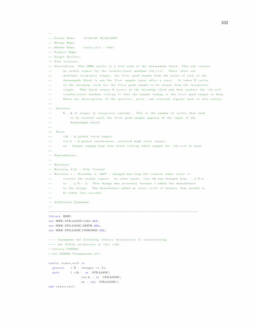
102
−−
−− Create Date : 12 : 00 : 00 08/02/2007
−− Design Name :
−− Module Name : s t a r t c t r l − behv
−− Pro j ec t Name :
−− Target Devices :
−− Tool v e r s i on s :
−− Desc r ip t i on : This VHDL ent i t y i s a l e a f node o f the downsample block . This job c r e a t e s
−− an enable s i g n a l f o r the counter / s t a t e machine c l k c t r l . S ince there are
−− mult ip l e i n t e g r a t o r stages , the f i r s t good sample from the point o f view o f the
−− downsample block i s not the f i r s t sample input a f t e r a r e s e t . I t takes N cy c l e s
−− o f the incoming c l ock f o r the f i r s t good sample to be output from the i n t e g r a t o r
−− s t age s . This block counts N cy c l e s o f the incoming c l ock and then enab le s the c l k c t r l
−− counter / s t a t e machine t e l l i n g i t that the sample coming i s the f i r s t good sample to keep .
−− Below are d e s c r i p t i o n s o f the gene r i c s , ports , and i n t e r n a l s i g n a l s used in t h i s en t i t y .
−−
−− Gener ics
−− N : # of s t age s in i n t e g r a t o r cascade . This i s the number o f c y c l e s that need
−− to be counted un t i l the f i r s t good sample appears at the input o f the
−− downsample block .
−−
−− Ports
−− c l k : A g l oba l c l o ck s i g n a l .
−− r s t h : A g l oba l synchronous , a s s e r t ed high r e s e t s i g n a l .
−− en : Output coming from th i s block t e l l i n g which sample f o r c l k c t r l to keep .
−−
−− Dependencies :
−−
−− Revis ion :
−− Revis ion 0 .01 − F i l e Created
−− Revis ion 1 − November 4 , 2007 − changed how long the counter waits un t i l i t
−− c r e a t e s the enable s i g n a l . In other words , l i n e 68 was changed from . . .≤ N−3
−− to . . .≤ N − 2 . This change was neces sa ry because I added the demodulator
−− to the des ign . The demodulator added an extra cyc l e o f l a t ency that needed to
−− be taken in to account .
−−
−− Addit iona l Comments :
−−
−−−−−−−−−−−−−−−−−−−−−−−−−−−−−−−−−−−−−−−−−−−−−−−−−−−−−−−−−−−−−−−−−−−−−−−−−−−−−−−−−−
l i b r a r y IEEE ;
use IEEE . STD LOGIC 1164 .ALL;
use IEEE .STD LOGIC ARITH.ALL;
use IEEE .STD LOGIC UNSIGNED.ALL;
−−−− Uncomment the f o l l ow ing l i b r a r y d e c l a r a t i on i f i n s t a n t i a t i n g
−−−− any Xi l inx p r im i t i v e s in t h i s code .
−−l i b r a r y UNISIM ;
−−use UNISIM . VComponents . a l l ;
e n t i t y s t a r t c t r l i s
g ene r i c ( N : i n t e g e r := 5 ) ;
port ( c l k : in STD LOGIC;
r s t h : in STD LOGIC;
en : out STD LOGIC) ;
end s t a r t c t r l ;

103
a r ch i t e c t u r e behv o f s t a r t c t r l i s
s i g n a l count : i n t e g e r range 0 to N; −− c r ea t e an i n t e g e r s i g n a l o f c o r r e c t s i z e
begin
s ta r tup count : p roce s s ( c l k )
begin
i f c lk ' event and c lk = '1 ' then −− count p o s i t i v e edges o f incoming c l ock
i f r s t h = '1 ' then −− c r ea t e an a s s e r t ed high , synchronous r e s e t
count ≤ 0 ;
en ≤ '0 ' ;
e l s e
i f count ≤ N − 2 then −− i f count i s ≤ N − 2 , keep counting
count ≤ count + 1 ;
en ≤ '0 ' ;
e l s e −− as soon as count reaches N − 1 , stop counting and a s s e r t en
en ≤ '1 ' ;
end i f ; −− count ≤ N − 3
end i f ; −− r s t h = '1 '
end i f ; −− clk ' event and c lk = '1 '
end proce s s s ta r tup count ;
end behv ;
ce reg.vhd
−−−−−−−−−−−−−−−−−−−−−−−−−−−−−−−−−−−−−−−−−−−−−−−−−−−−−−−−−−−−−−−−−−−−−−−−−−−−−−−−−−
−− Company :
−− Engineer :
−−
−− Create Date : 11 : 42 : 25 08/02/2007
−− Design Name :
−− Module Name : c e r e g − behv
−− Pro j ec t Name :
−− Target Devices :
−− Tool v e r s i on s :
−− Desc r ip t i on : This VHDL ent i t y i s a gene ra l b i t width , p o s i t i v e edge t r i gge r ed ,
−− c l ock enabled D−type r e g i s t e r . This i s used f o r a l l r e g i s t e r s a f t e r the
−− downsample block . Below are d e s c r i p t i o n s o f the por t s and g en e r i c s used in
−− t h i s en t i t y .
−−
−− Gener ics
−− B ce reg : # of b i t s in the r e g i s t e r .
−−
−− Ports
−− c l k : A g l oba l c l o ck s i g n a l .
−− r s t h : A g l oba l synchronous , a s s e r t ed high r e s e t s i g n a l .
−− ce : A c lock enable s i g n a l . This s i g n a l i s c reated from the downsample block
−− and used to dr ive any r e g i s t e r that needs to operate at the d iv ided ra t e .
−− inp : The input to t h i s r e g i s t e r .
−− outp : The output o f t h i s r e g i s t e r .

104
−−
−− Dependencies :
−−
−− Revis ion :
−− Revis ion 0 .01 − F i l e Created
−− Addit iona l Comments :
−−
−−−−−−−−−−−−−−−−−−−−−−−−−−−−−−−−−−−−−−−−−−−−−−−−−−−−−−−−−−−−−−−−−−−−−−−−−−−−−−−−−−
l i b r a r y IEEE ;
use IEEE . STD LOGIC 1164 .ALL;
use IEEE .STD LOGIC ARITH.ALL;
use IEEE .STD LOGIC SIGNED.ALL;
−−−− Uncomment the f o l l ow ing l i b r a r y d e c l a r a t i on i f i n s t a n t i a t i n g
−−−− any Xi l inx p r im i t i v e s in t h i s code .
−−l i b r a r y UNISIM ;
−−use UNISIM . VComponents . a l l ;
e n t i t y c e r e g i s
g ene r i c ( B ce reg : i n t e g e r := 52 ) ;
port ( c l k : in STD LOGIC;
r s t h : in STD LOGIC;
ce : in STD LOGIC;
inp : in STD LOGIC VECTOR ( B ce reg − 1 downto 0 ) ;
outp : out STD LOGIC VECTOR ( B ce reg − 1 downto 0 ) ) ;
end c e r e g ;
a r c h i t e c t u r e behv o f c e r e g i s
begin
en reg : p roce s s ( c l k )
begin
i f c lk ' event and c lk = '1 ' then −− c r ea t e a p o s i t i v e edge t r i g g e r ed r e g i s t e r
i f r s t h = '1 ' then −− c r ea t e a synchronous , a s s e r t ed high r e s e t t a b l e r e g i s t e r
outp ≤ ( o the r s => ' 0 ' ) ;
e l s i f ce = '1 ' then −− c r ea t e a c l ock enabled r e g i s t e r
outp ≤ inp ;
end i f ; −− r s t h = '1 '
end i f ; −− clk ' event and c lk = '1 '
end proce s s en reg ;
end behv ;
coeffrom.vhd
−−−−−−−−−−−−−−−−−−−−−−−−−−−−−−−−−−−−−−−−−−−−−−−−−−−−−−−−−−−−−−−−−−−−−−−−−−−−−−−−−−
−− Company :
−− Engineer :
−−
−− Create Date : 16 : 33 : 41 08/13/2007
−− Design Name :
−− Module Name : coe f f rom − behv
−− Pro j ec t Name :

105
−− Target Devices :
−− Tool v e r s i on s :
−− Desc r ip t i on : This VHDL ent i t y i s a ROM module that i s i n i t i a l i z e d with the
−− contents o f a f i l e . This f i l e conta ins what each element should be
−− i n i t i a l i z e d to in b i t vec tor format . These f i l e s are c reated by the
−− MATLAB s c r i p t p o l y f i l t .m. The en t i t y uses an impure func t i on to i n i t i a l i z e
−− the rom array to the va lues conta ined in the f i l e . Below are d e s c r i p t i o n s
−− o f the gene r i c s , ports , and i n t e r n a l s i g n a l s used in t h i s en t i t y .
−−
−− Gener ics
−− N elems : The number o f e lements in the ROM.
−− B data : The b i t width o f the e lements s to red in the ROM.
−− B addr : The b i t width o f the address input to the ROM.
−− fname : The f i l e name that i s used to i n i t i a l i z e the ROM. This f i l e must
−− be in the same d i r e c t o r y as the en t i t y .
−−
−− Ports
−− c l k : The g l oba l c l o ck s i g n a l .
−− r s t h : The g l oba l synchronous , a s s e r t ed high r e s e t s i g n a l .
−− en : The enable s i g n a l that i s used to output new data at the CIC f i l t e r
−− output ra t e .
−− addr : The address input to the ROM.
−− rom out : The output data from the ROM.
−−
−− I n t e r na l S i gna l s
−− rom : This i s a constant s i g n a l that i s an ( N elems ) by ( B data ) arra
−− that s t o r e s the c o e f f i c i e n t s o f the f i l t e r .
−−
−− Dependencies :
−−
−− Revis ion :
−− Revis ion 0 .01 − F i l e Created
−− Addit iona l Comments :
−−
−−−−−−−−−−−−−−−−−−−−−−−−−−−−−−−−−−−−−−−−−−−−−−−−−−−−−−−−−−−−−−−−−−−−−−−−−−−−−−−−−−
l i b r a r y IEEE ;
use IEEE . STD LOGIC 1164 .ALL;
use IEEE .STD LOGIC ARITH.ALL;
use IEEE .STD LOGIC UNSIGNED.ALL;
use STD.TEXTIO.ALL;
−−−− Uncomment the f o l l ow ing l i b r a r y d e c l a r a t i on i f i n s t a n t i a t i n g
−−−− any Xi l inx p r im i t i v e s in t h i s code .
−−l i b r a r y UNISIM ;
−−use UNISIM . VComponents . a l l ;
e n t i t y coe f f rom i s
g ene r i c ( N elems : i n t e g e r := 8 ;
B data : i n t e g e r := 14 ;
B addr : i n t e g e r := 3 ;
fname : s t r i n g := ”rom0 . txt ” ) ;
port ( c l k : in STD LOGIC;
r s t h : in STD LOGIC;
en : in STD LOGIC;

106
addr : in STD LOGIC VECTOR ( B addr − 1 downto 0 ) ;
rom out : out STD LOGIC VECTOR ( B data − 1 downto 0 ) ) ;
end coe f f rom ;
a r c h i t e c t u r e behv o f coe f f rom i s
−− c r ea t e an i n t e r n a l rom array o f b i t v e c t o r type so i t can be i n i t i a l i z e d with a f i l e
type rom type i s array (0 to N elems − 1) o f b i t v e c t o r ( B data − 1 downto 0 ) ;
−− c r ea t e an impure func t i on to load the ram with a f i l e
impure func t i on load rom ( l o a d f i l e : in s t r i n g ) return rom type i s
f i l e r om f i l e : t ext open read mode i s l o a d f i l e ; −− open a f i l e in read mode
va r i ab l e l i n e i n : l i n e ; −− dec l a r e a l i n e va r i ab l e f o r read ing from f i l e
v a r i ab l e tmp rom : rom type ; −− dec l a r e a rom array to i n i t i a l i z e and then return
begin
f o r I in rom type ' range loop
r e ad l i n e ( r om f i l e , l i n e i n ) ; −− read from f i l e to l i n e va r i ab l e
read ( l i n e i n , tmp rom( I ) ) ; −− i n i t i a l i z e rom element to value from f i l e
end loop ;
re turn tmp rom ;
end func t i on load rom ;
−− c r ea t e a constant rom array and i n i t i a l i z e i t with contents o f f i l e fname
constant rom : rom type := load rom ( fname ) ;
begin −− arch . behv o f coe f f rom
read rom : proce s s ( c l k )
begin
i f c lk ' event and c lk = '1 ' then −− read on a posedge o f c l o ck
i f r s t h = '1 ' then −− output l a s t value o f ROM on a r e s e t
rom out ≤ t o s t d l o g i c v e c t o r ( rom( N elems − 1 ) ) ;
e l s i f en = '1 ' then −− output data accord ing to addr when en i s a s s e r t ed
rom out ≤ t o s t d l o g i c v e c t o r ( rom( conv in t eg e r ( addr ) ) ) ;
end i f ; −− r s t h = '1 '
end i f ; −− clk ' event and c lk = '1 '
end proce s s read rom ;
end behv ;
gen mult.vhd
−−−−−−−−−−−−−−−−−−−−−−−−−−−−−−−−−−−−−−−−−−−−−−−−−−−−−−−−−−−−−−−−−−−−−−−−−−−−−−−−−−
−− Company :
−− Engineer :
−−
−− Create Date : 17 : 01 : 47 08/07/2007
−− Design Name :
−− Module Name : gen mult − behv
−− Pro j ec t Name :
−− Target Devices :
−− Tool v e r s i on s :
−− Desc r ip t i on : This VHDL ent i t y i s a gener i c , s igned , f u l l p r e c i s i o n mu l t i p l i e r .
−− Below are d e s c r i p t i o n s o f the gene r i c s , ports , and i n t e r n a l s i g n a l s o f t h i s
−− en t i t y .
−−
−− Gener ics

107
−− B mult in1 : The b i t width o f the f i r s t input to the mu l t i p l i e r . In t h i s
−− design , t h i s i s the input to the polyphase FIR f i l t e r .
−− B mult in2 : The b i t width o f the second input to the mu l t i p l i e r . In t h i s
−− design , t h i s i s the output o f the tap ROMs.
−−
−− Ports
−− in1 : The f i r s t input to the mu l t i p l i e r .
−− in2 : The second input to the mu l t i p l i e r .
−− prod : The f u l l p r e c i s i on , s igned output o f the mu l t i p l i e r .
−−
−− I n t e r na l S i gna l s
−− There are no i n t e r n a l s i g n a l s in t h i s en t i t y .
−−
−− Dependencies :
−−
−− Revis ion :
−− Revis ion 0 .01 − F i l e Created
−− Addit iona l Comments :
−−
−−−−−−−−−−−−−−−−−−−−−−−−−−−−−−−−−−−−−−−−−−−−−−−−−−−−−−−−−−−−−−−−−−−−−−−−−−−−−−−−−−
l i b r a r y IEEE ;
use IEEE . STD LOGIC 1164 .ALL;
use IEEE .STD LOGIC ARITH.ALL;
use IEEE .STD LOGIC SIGNED.ALL;
−−−− Uncomment the f o l l ow ing l i b r a r y d e c l a r a t i on i f i n s t a n t i a t i n g
−−−− any Xi l inx p r im i t i v e s in t h i s code .
−−l i b r a r y UNISIM ;
−−use UNISIM . VComponents . a l l ;
e n t i t y gen mult i s
g ene r i c ( B mult in1 : i n t e g e r := 14 ;
B mult in2 : i n t e g e r := 16 ) ;
port ( in1 : in STD LOGIC VECTOR ( B mult in1 − 1 downto 0 ) ;
in2 : in STD LOGIC VECTOR ( B mult in2 − 1 downto 0 ) ;
prod : out STD LOGIC VECTOR (( B mult in1 + B mult in2 ) − 1 downto 0 ) ) ;
end gen mult ;
a r c h i t e c t u r e behv o f gen mult i s
begin
mult : p roce s s ( in1 , in2 )
begin
prod ≤ s igned ( in1 ) ∗ s igned ( in2 ) ;
end proce s s mult ;
end behv ;
accum D.vhd
−−−−−−−−−−−−−−−−−−−−−−−−−−−−−−−−−−−−−−−−−−−−−−−−−−−−−−−−−−−−−−−−−−−−−−−−−−−−−−−−−−
−− Company :
−− Engineer :

108
−−
−− Create Date : 14 : 48 : 26 08/07/2007
−− Design Name :
−− Module Name : accum D − behv
−− Pro j ec t Name :
−− Target Devices :
−− Tool v e r s i on s :
−− Desc r ip t i on : This VHDL ent i t y accumulates the input s i g n a l f o r D factor
−− c y c l e s . This en t i t y uses s igned ar i thmet i c to do t h i s . Also , t h i s en t i t y has
−− a c l ock enable s i g n a l because i t needs to accumulate at the CIC f i l t e r output
−− rate , not the g l oba l c l o ck ra t e . This en t i t y keeps f u l l p r e c i s i o n in the
−− accumulator , in other words , the re are s e v e r a l guard b i t s in the accumulator
−− to prevent over f l ow . Below are d e s c r i p t i o n s o f the gene r i c s , ports , and
−− i n t e r n a l s i g n a l s used in t h i s en t i t y .
−−
−− Gener ics
−− D factor : The decimation f a c t o r o f the polyphase FIR f i l t e r . This i s
−− the number o f c y c l e s that the input needs to be accumulated .
−− B acc in : The b i t width o f the input to the accumulator .
−− B acc out : The b i t width o f the output o f the accumulator . This i s a l s o
−− the b i t width o f the accumulator . This i s u sua l l y l a r g e r than
−− the input by s e v e r a l b i t s so that there are some guard b i t s
−− in the accumulator to prevent over f low .
−−
−− Ports
−− c l k : The g l oba l c l o ck s i g n a l .
−− r s t h : The g loba l , synchronous , a s s e r t ed high r e s e t s i g n a l .
−− c e i n : The c l ock enable s i g n a l used to operate the accumulator at the
−− CIC f i l t e r output ra t e in s t ead o f the f a s t e r g l oba l c l o ck ra t e .
−− a c c i n : The input to the accumulator . In t h i s des ign , t h i s i s the output
−− o f the tap mu l t i p l i e r .
−− acc out : The output o f the accumulator . This i s output at the polyphase
−− FIR f i l t e r output ra t e .
−−
−− I n t e r na l S i gna l s
−− accumulator : This s i g n a l i s used to keep the value o f the accumulated
−− input .
−− tmp : This s i g n a l i s a temporary r e g i s t e r that i s used to hold the value
−− o f the input when the counter ove r f l ows . This i s nece s sa ry because
−− without i t , the input that occurs on the cyc l e that the counter
−− ove r f l ows does not get accumulated . This r e g i s t e r s t o r e s the value
−− o f the input that occurs on the cy c l e that the counter ove r f l ows .
−− This value i s then added to the accumulator on the next cy c l e .
−− count : This s i g n a l i s a counter that i s used to keep track o f how many
−− c y c l e s the input has been accumulated .
−−
−− Dependencies :
−−
−− Revis ion :
−− Revis ion 0 .01 − F i l e Created
−− Addit iona l Comments :
−−
−−−−−−−−−−−−−−−−−−−−−−−−−−−−−−−−−−−−−−−−−−−−−−−−−−−−−−−−−−−−−−−−−−−−−−−−−−−−−−−−−−
l i b r a r y IEEE ;
use IEEE . STD LOGIC 1164 .ALL;

109
use IEEE .STD LOGIC ARITH.ALL;
use IEEE .STD LOGIC SIGNED.ALL;
−−−− Uncomment the f o l l ow ing l i b r a r y d e c l a r a t i on i f i n s t a n t i a t i n g
−−−− any Xi l inx p r im i t i v e s in t h i s code .
−−l i b r a r y UNISIM ;
−−use UNISIM . VComponents . a l l ;
e n t i t y accum D i s
g ene r i c ( D factor : i n t e g e r := 8 ;
B acc in : i n t e g e r := 18 ;
B acc out : i n t e g e r := 24 ) ;
port ( c l k : in STD LOGIC;
r s t h : in STD LOGIC;
c e i n : in STD LOGIC;
a c c i n : in STD LOGIC VECTOR ( B acc in − 1 downto 0 ) ;
acc out : out STD LOGIC VECTOR ( B acc out − 1 downto 0 ) ) ;
end accum D ;
a r ch i t e c t u r e behv o f accum D i s
−− f unc t i on d e c l a r a t i on f o r a s i gn extender . This i s needed to
−− s i gn extend the tmp r e g i s t e r output to the accumulator b i t
−− b i t width when i t i s added to the accumulator .
func t i on s ignextend ( num short : in STD LOGIC VECTOR ( B acc in − 1 downto 0) )
re turn STD LOGIC VECTOR i s
va r i ab l e tmp num : STD LOGIC VECTOR ( B acc out − 1 downto 0 ) ;
begin
tmp num( B acc in − 1 downto 0) := num short ;
s i g n ex t : f o r i in B acc in to B acc out − 1 loop
tmp num( i ) := num short ( B acc in − 1 ) ;
end loop s i gn ex t ;
re turn tmp num ;
end func t i on s ignextend ;
−− i n t e r n a l s i g n a l s
s i g n a l accumulator : STD LOGIC VECTOR ( B acc out − 1 downto 0 ) ;
s i g n a l tmp : STD LOGIC VECTOR ( B acc in − 1 downto 0 ) ;
s i g n a l count : i n t e g e r range 0 to D factor ;
begin
accum : proce s s ( c l k )
begin
i f c lk ' event and c lk = '1 ' then −− do everyth ing on posedge o f c l o ck
i f r s t h = '1 ' then −− c r ea t e a synchronous , a s s e r t ed high r e s e t
accumulator ≤ ( o the r s => ' 0 ' ) ;
count ≤ 0 ;
acc out ≤ ( o the r s => ' 0 ' ) ;
tmp ≤ ( o the r s => ' 0 ' ) ;
e l s i f c e i n = '1 ' then −− count when c e i n i s a s s e r t ed
i f count ≤ ( D factor − 2) then −− count f o r D factor −2 cy c l e s
count ≤ count + 1 ; −− increment counter
i f count = 0 then −− when counter over f lows , add tmp to the input
accumulator ≤ s igned ( s ignextend (tmp) ) + s igned ( s ignextend ( a c c i n ) ) ;
e l s e −− when counter hasn ' t overf lowed , add the input to the accumulator
accumulator ≤ s igned ( accumulator ) + s igned ( s ignextend ( a c c i n ) ) ;
end i f ; −− count = 0
e l s e −− r e s e t counter when count = D factor −1 and output accumulator

110
count ≤ 0 ;
acc out ≤ accumulator ;
accumulator ≤ ( o the r s => ' 0 ' ) ;
tmp ≤ a c c i n ;
end i f ; −− count ≤ ( D factor −2)
end i f ; −− r s t h = '1 '
end i f ; −− clk ' event and c lk = '1 '
end proce s s accum ;
end behv ;
gen adder.vhd
−−−−−−−−−−−−−−−−−−−−−−−−−−−−−−−−−−−−−−−−−−−−−−−−−−−−−−−−−−−−−−−−−−−−−−−−−−−−−−−−−−
−− Company :
−− Engineer :
−−
−− Create Date : 13 : 20 : 48 08/06/2007
−− Design Name :
−− Module Name : gen adder − behv
−− Pro j ec t Name :
−− Target Devices :
−− Tool v e r s i on s :
−− Desc r ip t i on : This VHDL ent i t y i s a g ene r i c s igned adder . This i s
−− a l e a f node o f the i n t e g r a t o r en t i t y . This adder i s used in the
−− accumulators o f the i n t e g r a t o r s t age s . I t i s important to note that t h i s
−− adder has no carry in or carry out port s . For t h i s design , i t i s assumed
−− that the accumulator b i t width i s s u f f i c i e n t to not inc lude these por t s .
−− Below are d e s c r i p t i o n s o f the gene r i c s , ports , and i n t e r n a l s i g n a l s that
−− are used in t h i s en t i t y .
−−
−− Gener ics
−− B adder : # of b i t s on input and output o f g ene r i c adder .
−−
−− Ports
−− add1 : The f i r s t input to be added toge the r .
−− add2 : The second input to be added toge the r .
−− sum : The r e s u l t o f adding add1 and add2 .
−−
−− I n t e r na l S i gna l s
−− This module has no i n t e r n a l s i g n a l s .
−−
−− Dependencies :
−−
−− Revis ion :
−− Revis ion 0 .01 − F i l e Created
−− Addit iona l Comments :
−−
−−−−−−−−−−−−−−−−−−−−−−−−−−−−−−−−−−−−−−−−−−−−−−−−−−−−−−−−−−−−−−−−−−−−−−−−−−−−−−−−−−
l i b r a r y IEEE ;
use IEEE . STD LOGIC 1164 .ALL;
use IEEE .STD LOGIC ARITH.ALL;

111
use IEEE .STD LOGIC SIGNED.ALL;
−−−− Uncomment the f o l l ow ing l i b r a r y d e c l a r a t i on i f i n s t a n t i a t i n g
−−−− any Xi l inx p r im i t i v e s in t h i s code .
−−l i b r a r y UNISIM ;
−−use UNISIM . VComponents . a l l ;
e n t i t y gen adder i s
g ene r i c ( B adder : i n t e g e r := 52 ) ;
port ( add1 : in STD LOGIC VECTOR ( B adder − 1 downto 0 ) ;
add2 : in STD LOGIC VECTOR ( B adder − 1 downto 0 ) ;
sum : out STD LOGIC VECTOR ( B adder − 1 downto 0 ) ) ;
end gen adder ;
a r c h i t e c t u r e behv o f gen adder i s
begin
add : p roce s s ( add1 , add2 )
begin
sum ≤ s igned ( add1 ) + s igned ( add2 ) ;
end proce s s add ;
end behv ;
gen subtractor.vhd
−−−−−−−−−−−−−−−−−−−−−−−−−−−−−−−−−−−−−−−−−−−−−−−−−−−−−−−−−−−−−−−−−−−−−−−−−−−−−−−−−−
−− Company :
−− Engineer :
−−
−− Create Date : 13 : 23 : 00 08/06/2007
−− Design Name :
−− Module Name : gen subt rac to r − behv
−− Pro j ec t Name :
−− Target Devices :
−− Tool v e r s i on s :
−− Desc r ip t i on : This VHDL ent i t y i s a g ene r i c B subtractor − b i t s igned subt rac to r .
−− This i s a l e a f node in the comb s t ru c tu r e o f the CIC f i l t e r . This en t i t y
−− r e s i d e s in the four th l e v e l o f h i e ra rchy in the des ign . Gen subtractor
−− sub t ra c t s sub2 from sub1 to c r ea t e d i f f . Below are d e s c r i p t i o n s o f the
−− g en e r i c s and port s used in t h i s module .
−−
−− Gener ics
−− B subtractor : # of b i t s on inputs and output o f module
−−
−− Ports
−− sub1 : Number that sub2 ge t s subtracted from .
−− sub2 : Number that i s subtracted from sub1 .
−− d i f f : The d i f f e r e n c e o f sub1 and sub2 .
−−
−− Dependencies :

112
−−
−− Revis ion :
−− Revis ion 0 .01 − F i l e Created
−− Addit iona l Comments :
−−
−−−−−−−−−−−−−−−−−−−−−−−−−−−−−−−−−−−−−−−−−−−−−−−−−−−−−−−−−−−−−−−−−−−−−−−−−−−−−−−−−−
l i b r a r y IEEE ;
use IEEE . STD LOGIC 1164 .ALL;
use IEEE .STD LOGIC ARITH.ALL;
use IEEE .STD LOGIC UNSIGNED.ALL;
−−−− Uncomment the f o l l ow ing l i b r a r y d e c l a r a t i on i f i n s t a n t i a t i n g
−−−− any Xi l inx p r im i t i v e s in t h i s code .
−−l i b r a r y UNISIM ;
−−use UNISIM . VComponents . a l l ;
e n t i t y gen subt rac to r i s
g ene r i c ( B subtractor : i n t e g e r := 52 ) ;
port ( sub1 : in STD LOGIC VECTOR ( B subtractor − 1 downto 0 ) ;
sub2 : in STD LOGIC VECTOR ( B subtractor − 1 downto 0 ) ;
d i f f : out STD LOGIC VECTOR ( B subtractor − 1 downto 0 ) ) ;
end gen subt rac to r ;
a r c h i t e c t u r e behv o f gen subt rac to r i s
begin
sub : p roce s s ( sub1 , sub2 )
begin
d i f f ≤ s igned ( sub1 ) − s igned ( sub2 ) ;
end proce s s sub ;
end behv ;
gen reg.vhd
−−−−−−−−−−−−−−−−−−−−−−−−−−−−−−−−−−−−−−−−−−−−−−−−−−−−−−−−−−−−−−−−−−−−−−−−−−−−−−−−−−
−− Company :
−− Engineer :
−−
−− Create Date : 17 : 44 : 10 07/03/2007
−− Design Name :
−− Module Name : gen reg − behv
−− Pro j ec t Name :
−− Target Devices :
−− Tool v e r s i on s :
−− Desc r ip t i on : This VHDL ent i t y i s a B−b i t p o s i t i v e edge t r i g g e r ed r e g i s t e r with an
−− asynchronous , a s s e r t ed high r e s e t s i g n a l . This i s used f o r the accumulator
−− r e g i s t e r s in the i n t e g r a t o r cascade o f the CIC f i l t e r . Below are d e s c r i p t i o n s
−− o f the gene r i c s , ports , and i n t e r n a l s i g n a l s that are used in t h i s en t i t y .
−−
−− Gener ics

113
−− B : # of b i t s in r e g i s t e r .
−−
−− Ports
−− c lk : A g l oba l c l o ck .
−− r s t h : A globa l , synchronous , a s s e r t ed high r e s e t s i g n a l
−− inp : Input to the r e g i s t e r .
−− outp : Output o f the r e g i s t e r .
−−
−− I n t e r na l S i gna l s
−− There are no i n t e r n a l s i g n a l s in t h i s en t i t y .
−−
−− Dependencies :
−−
−− Revis ion :
−− Revis ion 0 .01 − F i l e Created
−− 0 .02 − changed from asynchronous r e s e t to synchronous r e s e t , s t i l l
−− a s s e r t ed high .
−− Addit iona l Comments :
−−
−−−−−−−−−−−−−−−−−−−−−−−−−−−−−−−−−−−−−−−−−−−−−−−−−−−−−−−−−−−−−−−−−−−−−−−−−−−−−−−−−−
l i b r a r y IEEE ;
use IEEE . STD LOGIC 1164 .ALL;
use IEEE .STD LOGIC ARITH.ALL;
use IEEE .STD LOGIC UNSIGNED.ALL;
−−−− Uncomment the f o l l ow ing l i b r a r y d e c l a r a t i on i f i n s t a n t i a t i n g
−−−− any Xi l inx p r im i t i v e s in t h i s code .
−−l i b r a r y UNISIM ;
−−use UNISIM . VComponents . a l l ;
e n t i t y gen reg i s
g ene r i c ( B : i n t e g e r := 52 ) ;
port ( c l k : in STD LOGIC;
r s t h : in STD LOGIC;
inp : in STD LOGIC VECTOR(B − 1 downto 0 ) ;
outp : out STD LOGIC VECTOR(B − 1 downto 0 ) ) ;
end gen reg ;
a r c h i t e c t u r e behv o f gen reg i s
begin
reg : p roce s s ( c l k )
begin
i f c lk ' event and c lk = '1 ' then −− c r ea t e a p o s i t i v e edge t r i g g e r ed r e g i s t e r
i f r s t h = '1 ' then −− c r ea t e a synchronous , a s s e r t ed high r e s e t
outp ≤ ( o the r s => ' 0 ' ) ;
e l s e
outp ≤ inp ; −− copy input to output on a p o s i t i v e edge
end i f ; −− r s t h = '1 '
end i f ; −− clk ' event and c lk = '1 '
end proce s s reg ;
end behv ;