Design and Implementation of Adiabatic Logic for Low Power ... · the inverter follows the power...
5
International Journal of Science and Research (IJSR) ISSN (Online): 2319-7064 Index Copernicus Value (2013): 6.14 | Impact Factor (2013): 4.438 Volume 4 Issue 8, August 2015 www.ijsr.net Licensed Under Creative Commons Attribution CC BY Design and Implementation of Adiabatic Logic for Low Power Application Vijendra Pratap Singh 1 , Dr. S. R. P. Sinha 2 1, 2 Institute of Engineering and Technology, Sitapur Road, Lucknow, India Abstract: This paper shows a new Adiabatic approach known as Complementary Pass Transistor Adiabatic Logic. Power minimization is the first priority of VLSI designers. The dynamic power requirement of CMOS circuits is a major concern in the design of personal information systems and large computers. The clocking mechanism used in Adiabatic logic is different from those of standard CMOS circuits. The Recovery phase of the power clock is used to recover charge from the load capacitor. Adiabatic logic provides a way to reuse the energy stored in load capacitors rather than the conventional way of discharging the load capacitors to the ground and wasting this energy. This paper shows the low power dissipation of Adiabatic logic by presenting the results of various designs (an inverter, two input AND gate, two input NAND gate, two input XOR gate). All simulations are carried out by TSPICE 14.1 and technology used is 90nm. Keywords: Adiabatic logic, CPAL , Energy Recovery, Static CMOS, Low Power, Energy dissipation, Power clock. 1. Introduction At present , the power consumption has become the major concern in the portable electronic devices such as mobile phones , laptops for VLSI designers. Due to the limited power of batteries, the circuitry involved in these devices must consume less power. Large power dissipation in these circuits requires costly and noisy cooling machinery. Several low power design techniques have been developed to reduce the power consumption in the conventional CMOS circuits. The energy dissipation in the conventional CMOS can be reduced by using Adiabatic Switching principle. By using the adiabatic switching principle, the power dissipation in the PMOS network can be minimized and energy stored at the load capacitor can be recovered rather than dissipated as heat. The circuits designed using Complementary Pass Transistor adiabatic logic (CPAL) [1] shows less power dissipation as compared to the conventional CMOS. 2. Adiabatic Switching Principle Figure 1 shows the equivalent circuit used to model the conventional CMOS [1] circuits during charging process of the output load capacitance. But in this figure, the constant voltage source is replaced with the constant current source to charge the load capacitance and discharge the load capacitance. Where R is the ON resistance of the PMOS network, C L is the load capacitance [1]. The energy dissipated in the resistance R [1] is given by- Since energy dissipation depends on the R, the ON resistance of the PMOS network. So by reducing the ON resistance of PMOS, energy dissipation can be minimized. The ON resistance [3] of MOS transistor is given by- Where μ is the mobility, C ox is the oxide capacitance, V GS is the gate to source voltage, V TH is the threshold voltage. Dissipated energy also depends on the charging time constant T, if T >>2RC [2] then energy dissipation will be very less as compared to conventional CMOS. Figure1: Constant current source charging a load capacitance, through resistance R.. The energy stored at the load capacitance can be recovered by simply reversing the current direction during discharging process instead of dissipation in the NMOS network. 3. Adiabatic digital logic circuits Practically, there are basically two types of Adiabatic logic circuits defined that is Partially Adiabatic and Fully Adiabatic. In partially Adiabatic logic all charge cannot be recovered by the power clock (pck) that is some charge Is transferred to the ground but in the fully Adiabatic logic based circuits all charge from the load capacitance is recovered by the power clock. In literature, different logic families [1-5] such as Efficient Charge Recovery Logic (ECRL), 2N- 2N2P Adiabatic Logic, Positive Feedback Adiabatic Logic (PFAL), NMOS Energy Recovery Logic (NERL), Clocked Adiabatic Logic (CAL), True Single-Phase Adiabatic Logic (TSEL), Source-coupled Adiabatic Logic (SCAL), Two phase adiabatic static CMOS logic (2PASCL) and Complementary Pass Transistor Adiabatic Logic (CPAL) are given. But in this paper we are using Complementary Pass Transistor Adiabatic Logic (CPAL) for design purpose, Paper ID: SUB157441 930
Transcript of Design and Implementation of Adiabatic Logic for Low Power ... · the inverter follows the power...

International Journal of Science and Research (IJSR) ISSN (Online): 2319-7064
Index Copernicus Value (2013): 6.14 | Impact Factor (2013): 4.438
Volume 4 Issue 8, August 2015
www.ijsr.net Licensed Under Creative Commons Attribution CC BY
Design and Implementation of Adiabatic Logic for
Low Power Application
Vijendra Pratap Singh1, Dr. S. R. P. Sinha
2
1, 2Institute of Engineering and Technology, Sitapur Road, Lucknow, India
Abstract: This paper shows a new Adiabatic approach known as Complementary Pass Transistor Adiabatic Logic. Power
minimization is the first priority of VLSI designers. The dynamic power requirement of CMOS circuits is a major concern in the design
of personal information systems and large computers. The clocking mechanism used in Adiabatic logic is different from those of
standard CMOS circuits. The Recovery phase of the power clock is used to recover charge from the load capacitor. Adiabatic logic
provides a way to reuse the energy stored in load capacitors rather than the conventional way of discharging the load capacitors to the
ground and wasting this energy. This paper shows the low power dissipation of Adiabatic logic by presenting the results of various
designs (an inverter, two input AND gate, two input NAND gate, two input XOR gate). All simulations are carried out by TSPICE 14.1
and technology used is 90nm.
Keywords: Adiabatic logic, CPAL , Energy Recovery, Static CMOS, Low Power, Energy dissipation, Power clock.
1. Introduction
At present , the power consumption has become the major
concern in the portable electronic devices such as mobile
phones , laptops for VLSI designers. Due to the limited
power of batteries, the circuitry involved in these devices
must consume less power. Large power dissipation in these
circuits requires costly and noisy cooling machinery. Several
low power design techniques have been developed to reduce
the power consumption in the conventional CMOS circuits.
The energy dissipation in the conventional CMOS can be
reduced by using Adiabatic Switching principle. By using
the adiabatic switching principle, the power dissipation in the
PMOS network can be minimized and energy stored at the
load capacitor can be recovered rather than dissipated as
heat. The circuits designed using Complementary Pass
Transistor adiabatic logic (CPAL) [1] shows less power
dissipation as compared to the conventional CMOS.
2. Adiabatic Switching Principle
Figure 1 shows the equivalent circuit used to model the
conventional CMOS [1] circuits during charging process of
the output load capacitance. But in this figure, the constant
voltage source is replaced with the constant current source to
charge the load capacitance and discharge the load
capacitance. Where R is the ON resistance of the PMOS
network, CL is the load capacitance [1]. The energy
dissipated in the resistance R [1] is given by-
Since energy dissipation depends on the R, the ON resistance
of the PMOS network. So by reducing the ON resistance of
PMOS, energy dissipation can be minimized. The ON
resistance [3] of MOS transistor is given by-
Where µ is the mobility, Cox is the oxide capacitance, VGS is
the gate to source voltage, VTH is the threshold voltage.
Dissipated energy also depends on the charging time constant
T, if T >>2RC [2] then energy dissipation will be very less as
compared to conventional CMOS.
Figure1: Constant current source charging a load
capacitance, through resistance R..
The energy stored at the load capacitance can be recovered
by simply reversing the current direction during discharging
process instead of dissipation in the NMOS network.
3. Adiabatic digital logic circuits
Practically, there are basically two types of Adiabatic logic
circuits defined that is Partially Adiabatic and Fully
Adiabatic. In partially Adiabatic logic all charge cannot be
recovered by the power clock (pck) that is some charge Is
transferred to the ground but in the fully Adiabatic logic
based circuits all charge from the load capacitance is
recovered by the power clock. In literature, different logic
families [1-5] such as Efficient Charge Recovery Logic
(ECRL), 2N- 2N2P Adiabatic Logic, Positive Feedback
Adiabatic Logic (PFAL), NMOS Energy Recovery Logic
(NERL), Clocked Adiabatic Logic (CAL), True Single-Phase
Adiabatic Logic (TSEL), Source-coupled Adiabatic Logic
(SCAL), Two phase adiabatic static CMOS logic (2PASCL)
and Complementary Pass Transistor Adiabatic Logic (CPAL)
are given. But in this paper we are using Complementary
Pass Transistor Adiabatic Logic (CPAL) for design purpose,
Paper ID: SUB157441 930
International Journal of Science and Research (IJSR) ISSN (Online): 2319-7064
Index Copernicus Value (2013): 6.14 | Impact Factor (2013): 4.438
Volume 4 Issue 8, August 2015
www.ijsr.net Licensed Under Creative Commons Attribution CC BY
because this logic reduced the power consumption compared
to other logic families.
3.1 Design and Simulation for Complementary Pass
Transistor Adiabatic Logic INVERTER
The two phase CPAL inverter is shown in figure 2. It is
mainly composed of two parts: Logic function circuit that
consists of four NMOS transistor with complementary pass
transistor logic function block, and the load drive circuit that
consists of pair of transmission gates. The CPAL inverter is
designed using TSPICE and simulated waveforms are shown
in figure2 and 3 respectively. The power dissipation against
different load capacitance is shown in figure 4.
Figure 2: Implementation of CPAL Inverter.
Where, a is the input of the inverter. When input is at logic
„1‟, the complemented output of the inverter follows the
power clock (Pclk) and output of the inverter is at logic „0‟.
In the same manner, when input is at logic „0‟, the output of
the inverter follows the power clock and shows the logic „1‟
at the output of the inverter.
Figure 3: Simulated waveforms of Adiabatic Inverter
Figure 4: Power dissipation (µW) vs Load Capacitance
3.2 Design and Simulation for Two input CPAL
AND/NAND GATE
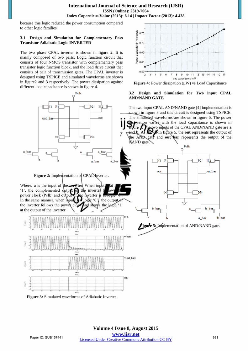
The two input CPAL AND/NAND gate [4] implementation is
shown in figure 5 and this circuit is designed using TSPICE.
The simulated waveforms are shown in figure 6. The power
dissipation varies with the load capacitance is shown in
figure 7. The two inputs of the CPAL AND/NAND gate are a
and b. As shown in figure 5, the out represents the output of
the AND gate and out_bar represents the output of the
NAND gate.
Figure 5: Implementation of AND/NAND gate.
Paper ID: SUB157441 931

International Journal of Science and Research (IJSR) ISSN (Online): 2319-7064
Index Copernicus Value (2013): 6.14 | Impact Factor (2013): 4.438
Volume 4 Issue 8, August 2015
www.ijsr.net Licensed Under Creative Commons Attribution CC BY
Figure 6: Simulated waveforms of CPAL AND/NAND Gate.
Figure 7: Power dissipation (µW) vs Load Capacitance
3.3 Design and Simulation for Two input CPAL
OR/NOR GATE
The two input CPAL OR/NOR gate [4] implementation is
shown in figure 8 and this circuit is designed using TSPICE.
The simulated waveforms are shown in figure 9. The power
dissipation varies with the load capacitance is shown in
figure 10. Where a and b represents the two inputs of CPAL
OR/NOR gate. As shown in figure 8, the out represents the
output of the OR gate and out_bar represents the output of
the NOR gate.
Figure 8: Implementation of CPAL OR/NOR gate
Figure 9: Simulated waveforms of CPAL OR/NOR Gate
Figure10: Power dissipation (µW) vs Load Capacitance.
3.4 Design and Simulation for Two input CPAL
XOR/XNOR GATE
The two input CPAL XOR/XNOR gate [4] implementation is
shown in figure 11 and this circuit is designed using TSPICE.
The simulated waveforms are shown in figure12. The power
dissipation varies with the load capacitance is shown in
figure 13. Where a and b represents the two inputs of CPAL
Paper ID: SUB157441 932

International Journal of Science and Research (IJSR) ISSN (Online): 2319-7064
Index Copernicus Value (2013): 6.14 | Impact Factor (2013): 4.438
Volume 4 Issue 8, August 2015
www.ijsr.net Licensed Under Creative Commons Attribution CC BY
XOR/XNOR gate. As shown in figure 11, the out represents
the output of XOR gate and out_bar represents the output of
the XNOR gate.
Figure11: Implementation of CPAL XOR/XNOR gate
Figure12: Simulated waveforms of CPAL XOR/XNOR
gate
Figure 13: Power dissipation (µW) vs Load Capacitance
4. Conclusion
The Complementary Pass Transistor adiabatic logic circuits
are preferred over conventional CMOS logic circuit because
a CPAL circuit shows power reduction for the same design.
The simulation results show that CPAL circuit can recover
the energy dissipated in the conventional CMOS circuits.
However CPAL circuits cannot suitable for the application
where high speed of operation is required.
References
[1] Rakesh Kumar Yadav, Ashwani K. Rana, Shweta
Chauhan, Deepesh Ranka, Kamalesh Yadav, “ Four
Phase Clocking Rule for Energy Efficient Digital
Circuits - An Adiabatic Concept,” National Institute of
Technology, Hamirpur India,2011 IEEE.
[2] W. C. Athas, L.J. Svensson, J.G. Koller, N. Tzartzanis,
and E. Chou, “Low power digital systems based on
adiabatic switching principles,” IEEE Trans. VLSI
Systems, vol. 2, no. 4, pp. 398-407, Dec. 1994.
[3] J. S. Denker, “A review of adiabatic computing,” in
IEEE Symp. on Low Power Electronics pp. 94- 97,1994.
[4] Nikunj R Patel, Sarman K Hadia, “ Adiabatic Logic For
Low Power Application Using Design 180nm
Technology,”International Journal of Computer Trends
and Technology (IJCTT) – volume 4 Issue 4 –April
2013.
[5] Y. Moon and D.K. Jeong, “An efficient charge recover
logic circuit,” IEEE J. Solid-State Circuits, vol. 31, no.
4, pp. 514–522, Apr. 1996.
[6] A.G. Dickinson and J.S. Denker, “Adiabatic dynamic
logic,” IEEE J. Solid-state Circuits, vol. 30, pp. 311-
355, Mar. 1995.
[7] Arjun Mishra, Neha Singh, “Low Power Circuit Design
using Positive Feedback Adiabatic Logic (PFAL),” International Journal of Science and Research (IJSR) -
Volume 3 Issue 6, June 2014
[8] A. Vetuli, S. Di Pascoli, L.M. Reyneri, “Positive
Feedback in adiabatic logic”, Electronics Letters, Vol.
32 Issue 20, pp. 1867-1869, September 1996.
[9] Xiaoyan Luo, Wei Cheng, Jianping Hu,
“Complementary Pass-Transistor Adiabatic Logic with
Dual-Threshold CMOS and Gate-Length Biasing
Techniques for Leakage Reduction”, International
Journal of Digital Content Technology and its
Applications (JDCTA), Volume7, Number5, March
2013.
Author Profile
Vijendra Pratap Singh, received the B.Tech degree in Applied
Electronics and Instrumentation Engineering from Skyline Institute
of Engineering and Technology, Greater Noida, Uttar Pradesh,
India. He is currently final year student of M.Tech in Micro-
Electronics from, Institute of Engineering and Technology,
Lucknow. His area of interest includes Micro-Electronics and
VLSI.
Paper ID: SUB157441 933

International Journal of Science and Research (IJSR) ISSN (Online): 2319-7064
Index Copernicus Value (2013): 6.14 | Impact Factor (2013): 4.438
Volume 4 Issue 8, August 2015
www.ijsr.net Licensed Under Creative Commons Attribution CC BY
Dr. S.R.P Sinha received the B.Tech degree from, Ranchi
University in 1981 and M.Tech degree from, University of
Roorkee in 1984. He received the Ph.D degree from Lucknow
University in 2004. He is presently working as Associate Professor
in Department of Electronics Engineering, in Institute of
engineering and technology, Lucknow. His area of interest includes
Solid State Electronic Devices, Micro-Electronics and VLSI.
Paper ID: SUB157441 934