DESIGN AND FABRICATION OF AN INFRARED OPTICAL …cmosedu.com/jbaker/students/theses/Design and...
118
DESIGN AND FABRICATION OF AN INFRARED OPTICAL PYROMETER ASIC AS A DIAGNOSTIC FOR SHOCK PHYSICS EXPERIMENTS By Jared Gordon Bachelor of Science in Electrical Engineering University of Nevada Las Vegas 2009 A thesis submitted in partial fulfillment of the requirements for the Master of Science in Electrical Engineering Department of Electrical and Computer Engineering College of Engineering The Graduate College University of Nevada Las Vegas December 2013
Transcript of DESIGN AND FABRICATION OF AN INFRARED OPTICAL …cmosedu.com/jbaker/students/theses/Design and...

DESIGN AND FABRICATION OF AN INFRARED OPTICAL PYROMETER ASIC
AS A DIAGNOSTIC FOR SHOCK PHYSICS EXPERIMENTS
By
Jared Gordon
Bachelor of Science in Electrical Engineering
University of Nevada Las Vegas
2009
A thesis submitted in partial fulfillment
of the requirements for the
Master of Science in Electrical Engineering
Department of Electrical and Computer Engineering
College of Engineering
The Graduate College
University of Nevada Las Vegas
December 2013


------------------------------------------------------------------------------------------------------------
Copyright by Jared Gordon, 2014
All Rights Reserved
------------------------------------------------------------------------------------------------------------

ii
THE GRADUATE COLLEGE
We recommend the thesis prepared under our supervision by
Jared Gordon
entitled
Design and Fabrication of an Infrared Optical Pyrometer Asic as a
Diagnostic for Shock Physics Experiments
is approved in partial fulfillment of the requirements for the degree of
Master of Science in Electrical Engineering
Department of Electrical and Computer Engineering
R. Jacob Baker, Ph.D., Committee Chair
Peter Stubberud, Ph.D., Committee Member
Rama Venkat, Ph.D., Committee Member
Evangelo Yfantis, Ph.D., Graduate College Representative
Kathryn Hausbeck Korgan, Ph.D., Interim Dean of the Graduate College
December 2013

iii
ABSTRACT
Optical pyrometry is the sensing of thermal radiation emitted from an object using a
photoconductive device to convert photons into electrons, and is an important diagnostic
tool in shock physics experiments. Data obtained from an optical pyrometer can be used
to generate a blackbody curve of the material prior to and after being shocked by a high
speed projectile. The sensing element consists of an InGaAs photodiode array, biasing
circuitry, and multiple transimpedance amplifiers to boost the weak photocurrent from
the noisy dark current into a signal that can eventually be digitized. Once the circuit
elements have been defined, more often than not commercial-off-the-shelf (COTS)
components are inadequate to satisfy every requirement for the diagnostic, and therefore
a custom application specific design has to be considered. This thesis outlines the initial
challenges with integrating the photodiode array block with multiple COTS
transimpedance amplifiers onto a single chip, and offers a solution to a comparable
optical pyrometer that uses the same type of photodiodes in conjunction with a re-
designed transimpedance amplifier integrated onto a single chip. The final design
includes a thorough analysis of the transimpedance amplifier along with modeling the
circuit behavior which entails schematics, simulations, and layout. An alternative circuit
is also investigated that incorporates an approach to multiplex the signals from each
photodiode onto one data line and not only increases the viable real estate on the chip, but
also improves the behavior of the photodiodes as they are subjected to less thermal load.
The optical pyrometer application specific integrated circuit (ASIC) for shock physic
experiments includes a transimpedance amplifier (TIA) with a 100 kΩ gain operating at

iv
bandwidth of 30 MHz, and an input-referred noise RMS current of 50 nA that is capable
of driving a 50 Ω load.

v
ACKNOWLEDGEMENTS
My family means everything to me, and without their unconditional love and
continued support I do not think I could have ever done this. I especially thank my wife
for having to put up with my obsession with work and school. This will only be worth it
if it makes me a better husband and father. I would also like to thank my coworkers who
have provided such great insight, and have given me the perspective to continue on with
my studies. Especially Tom Waltman, who was instrumental in me pursuing this type of
research. I cannot thank him enough for how supportive he has been. Certainly I could
never forget thanking Jake Baker. Dr. Baker has served as my professor, thesis adviser,
but most of all as a friend. His instruction and guidance made what I considered a year
ago as a hopeless endeavor all the more possible. There has not been a single moment
during my long nights of writing when I felt any of this work to be a burden, and I
believe much of that has to do with Jake showing me the bigger picture of what will be
pursued and accomplished in years to come. This research will continue because of the
need for technological innovation at work, the willingness of those that I work with, the
foresight of my committee, and the tenacity of those wanting to see this through. For all
of these things and much more, I truly thank you all.

vi
DEDICATION
For my wife Janae, my son Ethan, and my daughters Gabrielle and Layla,
you are my inspiration.
I love you.

vii
TABLE of CONTENTS
ABSTRACT ................................................................................................................................... iii
ACKNOWLEDGEMENTS ............................................................................................................. v
DEDICATION ................................................................................................................................ vi
LIST of TABLES ........................................................................................................................... ix
LIST of FIGURES .......................................................................................................................... x
CHAPTER 1 - INTRODUCTION ................................................................................................... 1
1.1 BACKGROUND ......................................................................................................... 1
1.2 MOTIVATION ........................................................................................................... 2
1.3 THESIS ORGANIZATION ........................................................................................ 3
CHAPTER 2 – PHOTODIODE BACKGROUND ......................................................................... 5
2.1 PN PHOTODIODE ..................................................................................................... 5
2.2 PIN PHOTODIODE .................................................................................................... 8
2.3 AVALANCHE PHOTODIODE ................................................................................. 9
CHAPTER 3 – TRANSIMPEDANCE AMPLIFIER BACKGROUND ....................................... 12
3.1 SHUNT-SHUNT FEEDBACK OPEN-LOOP GAIN VERIFICATION .................. 17
3.2 GENERIC TIA SIMULATION ................................................................................ 21
3.3 IMPROVED TIA CIRCUIT ..................................................................................... 24
3.3.1 IMPROVED TIA OPEN-LOOP GAIN VERIFICATION ..................... 26
3.3.2 IMPROVED TIA DESIGN ENCAPSULATION .................................. 33
CHAPTER 4 – NOISE................................................................................................................... 37
4.1 THERMAL NOISE ................................................................................................... 38
4.2 SHOT NOISE ............................................................................................................ 42
4.2.1 DARK CURRENT ................................................................................. 44
4.2.2 PHOTON NOISE ................................................................................... 44
4.2.3 NOISE EQUIVALENT POWER ........................................................... 46
4.3 FLICKER NOISE .................................................................................................... 47
4.4 TREATMENT OF NOISE IN IMPROVED TIA CIRCUIT ................................... 49
4.4.1 THE TREATMENT OF NOISE IN CURRENT MIRRORS ................. 49
4.4.2 INPUT-REFERRED NOISE IN MULTI-STAGE AMPLIFIERS ......... 52
4.4.3 PHOTODIODE INPUT-REFERRED NOISE IMPACT ....................... 53
4.5 IMPROVED TIA CIRCUIT NOISE ANALYSIS ................................................... 56

viii
CHAPTER 5 – SIMULATION AND TESTING RESULTS ........................................................ 63
5.1 IMPROVED TIA FINAL SIMULATION RESULTS .............................................. 63
5.2 IMPROVED TIA CIRCUIT TEST RESULTS ......................................................... 74
5.3 TIA FINAL DESIGN ................................................................................................ 89
5.4 TRANSIMPEDANCE AMPLIFIER LAYOUT ....................................................... 96
CHAPTER 6 – CONCLUSIONS AND FUTURE WORK ........................................................... 98
REFERENCES ............................................................................................................................ 100
VITA ............................................................................................................................................ 102

ix
LIST of TABLES
Table 3-1. Operational point analysis results for the improved TIA ............................................ 27
Table 4-1. PD RMS input-referred noise ....................................................................................... 55
Table 5-1. Input pulse parameters ............................................................................................. 66
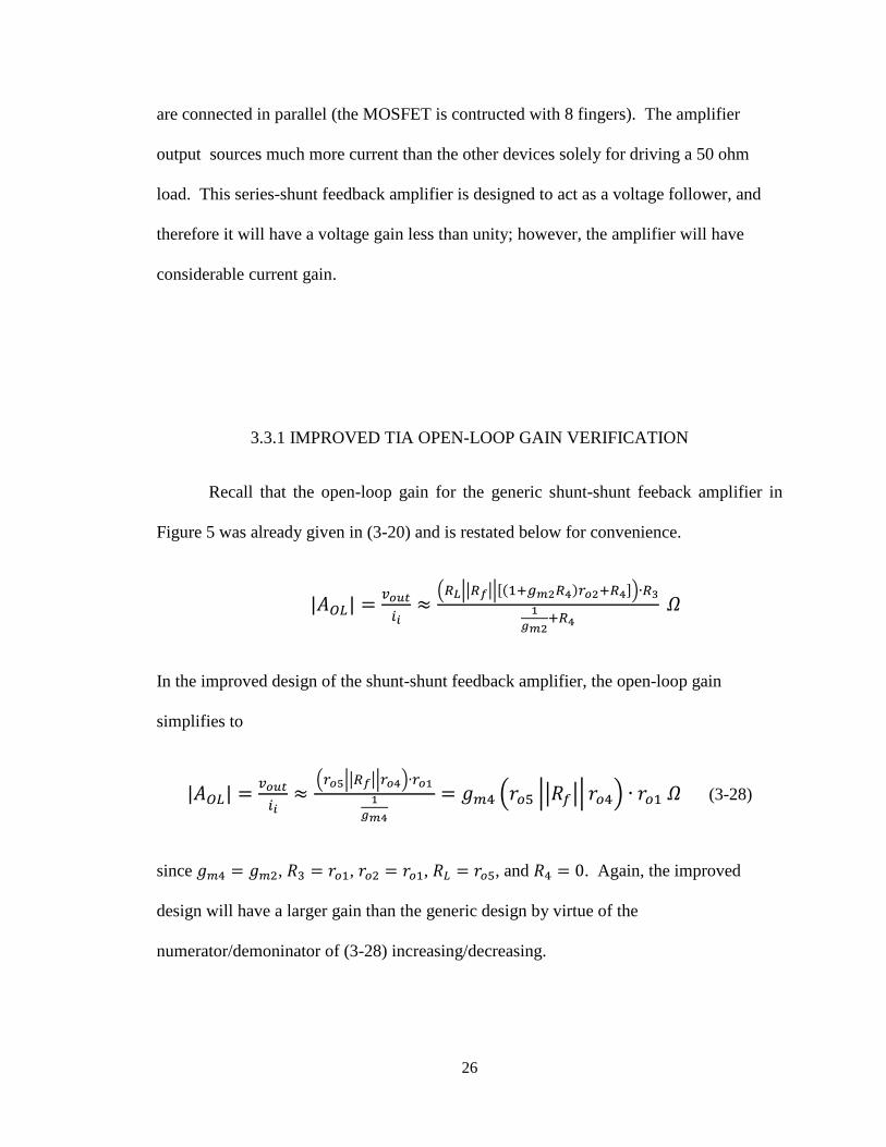
Table 5-2. Equipment fielded for TIA test ............................................................................... 76
Table 5-3. TIA test theoretical and measured results .............................................................. 83

x
LIST of FIGURES
Figure 1. pn photodiode cross section ............................................................................................. 5
Figure 2. PIN photodiode cross section .......................................................................................... 8
Figure 3. APD photodiode cross section ....................................................................................... 10
Figure 4. Avalanche multiplication pictorial representation ......................................................... 11
Figure 5. Generic shunt-shunt feedback amplifier ........................................................................ 13
Figure 6. Shunt-shunt feedback amplifier open-loop small-signal model .................................... 15
Figure 7. Small-signal analysis to find vx in the generic shunt-shunt feedback amplifier ........... 18
Figure 8. Small-signal analysis to find vout/vx in the generic shunt-shunt feedback amplifier ... 19
Figure 9. Output impedance seen looking into drain M2 .............................................................. 20
Figure 10. Generic TIA AC analysis schematic ........................................................................... 22
Figure 11. Generic TIA OP analysis results ................................................................................. 22
Figure 12. Generic TIA open-loop gain plot from the AC analysis .............................................. 23
Figure 13. Improved TIA design .................................................................................................. 25
Figure 14. AC analysis plot of the open-loop gain for the improved shunt-shunt amplifier ........ 28
Figure 15. DC operating point nodal voltages .............................................................................. 29
Figure 16. Series-shunt feedback amplifier small-signal model .................................................... 30
Figure 17. AC analysis plot of the open-loop gain for the series-shunt amplifier ........................ 32

xi
Figure 18. AC analysis schematic of the open-loop gain for the series-shunt amplifier .............. 33
Figure 19. AC analysis plot of the closed-loop gain for the shunt-shunt amplifier ...................... 34
Figure 20. AC analysis plot of the closed-loop gain for the series-shunt amplifier ...................... 35
Figure 21. AC analysis plot of the closed-loop gain for the TIA .................................................. 36
Figure 22. Thermal noise models .................................................................................................. 39
Figure 23. Shot noise model ......................................................................................................... 40
Figure 24. Shot noise generation .................................................................................................. 43
Figure 25. Flicker noise PSD ........................................................................................................ 47
Figure 26. MOSFET noise model ................................................................................................. 49
Figure 27. Simple current mirror noise model .............................................................................. 50
Figure 28. Output-referred noise for a simple current mirror ....................................................... 50
Figure 29. Cascode current mirror with noise ............................................................................... 52
Figure 30. Output-referred noise of a single amplifier ................................................................. 53
Figure 31. PD input noise ............................................................................................................. 54
Figure 32. TIA noise model .......................................................................................................... 56
Figure 33. Improved TIA noise model ......................................................................................... 58
Figure 34. TIA noise analysis schematic ...................................................................................... 61
Figure 35. Voltage spectral density noise plot for MB1 an M1 .................................................... 61

xii
Figure 36. Thermal noise contribution in the TIA due to MOSFETs M1 through M5 ....... 62
Figure 37. Improved TIA circuit DC analysis ......................................................................... 64
Figure 38. Input terminal DC sweep of the improved TIA ...................................................... 64
Figure 39. Output terminal DC sweep of the improved TIA ................................................... 65
Figure 40. Improved TIA circuit schematic with PD model .................................................. 65
Figure 41. Output signals produced by Ipeak currents ........................................................... 67
Figure 42. Improved TIA noise analysis schematic ................................................................ 67
Figure 43. Output noise measurent for the Improved TIA circuit ......................................... 68
Figure 44. Output noise RMS voltage for the Improved TIA circuit ................................... 69
Figure 45. Gain vs. frequency for the Improved TIA circuit ................................................. 69
Figure 46. Open-loop gain of the shunt-shunt feedback amplifier with 𝑅𝑓 = 25 𝑘𝛺 ........ 71
Figure 47. Open-loop gain of the series-shunt feedback amplifier ....................................... 72
Figure 48. Shunt-shunt feedback amplifier open-loop gain ........................................................ 73
Figure 49. Series-shunt feedback amplifier open-loop gain ....................................................... 73
Figure 50. Improved TIA circuit bare die chip ........................................................................ 75
Figure 51. Test circuit schematic ............................................................................................... 75
Figure 52. Test bench .................................................................................................................. 76

xiii
Figure 53. Top level view of DIP .............................................................................................. 77
Figure 54. DG535 input voltage pulse #1 at 5x attenuation and 844 ns pulse width ......... 79
Figure 55. 8082A input voltage pulse #2 at < 5ns pulsewidth .............................................. 79
Figure 56. 8082A input voltage pulse #3 at < 10ns pulsewidth ............................................ 80
Figure 57. Output pulse #1 .......................................................................................................... 81
Figure 58. Output pulse #2 .......................................................................................................... 81
Figure 59. Output pulse #3 .......................................................................................................... 82
Figure 60. Output pulse #4 .......................................................................................................... 82
Figure 61. Improved TIA schematic with emphasis on the current mirror .......................... 84
Figure 62. Improved TIA schematic with a negative increase in the M1 gate potential .... 85
Figure 63. Transient analysis results of a positive increase in the M1 gate potential ......... 85
Figure 64. Transient analysis results of a 1 μm increase in the channel width of M1 ......... 86
Figure 65. Transient analysis results of a 1 μm decrease in the channel width of M1 ........ 87
Figure 66. Spectrum analyzer output noise measurement of the improved TIA ................... 88
Figure 67. Final TIA design for the optical pyrometer ASIC ....................................................... 90
Figure 68. Final TIA op-amp schematic ....................................................................................... 91
Figure 69. Final TIA DC analysis schematic ................................................................................ 93
Figure 70. Final TIA DC analysis gain expectation with an 𝑅𝑏𝑖𝑎𝑠 = 5 𝑘𝛺 .................................. 93

xiv
Figure 71. Final TIA transient analysis with an 𝑅𝑏𝑖𝑎𝑠 = 5 𝑘𝛺 ..................................................... 94
Figure 72. Final TIA transient analysis with an 𝑅𝑏𝑖𝑎𝑠 = 20 𝑘𝛺 ................................................... 94
Figure 73. Final TIA transient analysis with an 𝑅𝑏𝑖𝑎𝑠 = 2 𝑘𝛺, and 𝑅𝑓 = 25 𝑘𝛺 ......................... 95
Figure 74. Final TIA closed-loop gain with an 𝑅𝑓 = 100 𝑘𝛺 ...................................................... 95
Figure 75. Final TIA output noise PSD with an 𝑅𝑓 = 100 𝑘𝛺 ..................................................... 96
Figure 76. Layout of the final TIA ................................................................................................ 97
Figure 77. Chip layout 1.5 𝑚𝑚 × 1.5 𝑚𝑚 ............................................................................... 97

1
CHAPTER 1 – INTRODUCTION
1.1 BACKGROUND
In shock wave physics experiments, dynamic temperature measurements are a critical
diagnostic tool that provides valuable information about a material’s state under shock
conditions [1]. To get real-time, in-situ temporal measurements, the diagnostic has to
map the shape of the black body temperature curve at multiple wavelengths within a short
record length. The basic elements of the diagnostic system include a photodiode
transducer to convert infrared thermal radiation to electricity, a transimpedance amplifier
(TIA) to convert the small photocurrent into a viable voltage signal, and an analog-to-
digital converter (ADC) to record the signal. The focus of this Thesis is a subsection of
the overall diagnostic system called an optical pyrometer which consists of an array of
photodetectors and a transimpedance amplifier.
Limitations in current commercial-off-the-shelf (COTS) technology has shifted the
focus away from assembling ad-hoc instrumentation with COTS components to
designing application specific integrated circuits (ASICs) in order to meet the increasing
design requirements of smaller footprints, higher bandwidth, and better noise
performance. An optical pyrometer ASIC chip solves the current problems of integrating
differing package types associated with the photodiode array sensing unit with multiple
TIAs; moreover, it allows a certain amount of flexibility in designing around a set of
requirements without sacrificing the performance from COTS components. In some
cases an ASIC chip design will reduce the footprint of the instrument and increase its

2
performance. The integration of the photodiode array with COTS transimpedance
amplifiers into an optical pyrometer instrument may increase the thermal loading on the
photodiode array. Thermal loading is an important factor that has to be considered in any
practical design as the photodiode package is susceptible to degradation in dynamic
resolution as a consequence to sharing chip real estate with a set of transimpedance
amplifiers. Without the knowledge a priori of the type of data achievable from such
experiments, that type of degradation in SNR can make the difference in the success of a
diagnostic.
1.2 MOTIVATION
The implementation of a successful experimental diagnostic is limited more often
than not by the technology that is available to both the scientist and engineer [2]. Many
times there have been cases where a diagnostic cannot be fielded because an instrument
has yet to be created to take the measurement of interest, or the COTS components that
are available are unsuitable. Characteristics that include, biasing, noise immunity, form
factor, and integration have to be carefully balanced in order to achieve a successful
diagnostic. The constraint of having to utilize COTS components can severely impact the
performance to the point where COTS are no longer a practical solution. This can result
in an experiment being delayed indefinitely, which can be costly to a company or
research lab.
Designing an optical pyrometer ASIC chip for shock physic experiments has two
advantages. The first advantage is that new types of diagnostics instrumentation that

3
have not been created thus far can be created in current technology, and the other is that
the small form factor reduces the usable real estate in the test chamber thereby increasing
the number of measurements. The impact of this technology spans both science and
engineering fields. These types of instrumentation ASICs create vast opportunities in
materials science as in-situ monitoring devices, and opens the door to analog and digital
chip designers who will be called upon to create innovative instrumentation designs.
1.3 THESIS ORGANIZATION
This Thesis describes the simulation, design, layout, and fabrication of an optical
pyrometer ASIC for shock physic experiments. Chapter 2 gives background information
on the photodiode, and emphasizes three different types that are likely to be used as the
sensing element in an optical pyrometer instrument. Chapter 3 provides a primer for the
TIA. Both the generic and improved TIA are discussed and compared in order to
demonstrate how simple adjustments can make significant improvements in the AC
performance. Concepts such as feedback, mixing-sampling topologies, and AC
characteristics that include open-loop and closed-loop gain are introduced. Calculations
of the AC parameters are compared with simulations in order to solidify the concepts.
Chapter 3 also discusses the TIA biasing circuitry, and introduces the cascode current
mirror. The chapter concludes with an encapsulation of the improved TIA closed-loop
gain. Chapter 4 covers the noise sources present in the optical pyrometer ASIC. Noise is
a limiting characteristic for any design, and this design is not an exception. Photodiode
shot noise, dark current, noise equivalent power, and MOSFET thermal and flicker noise

4
are all discussed. This chapter also discusses the noise modeling of the TIA along with
simulations of the output noise, and input-referred noise of the improved TIA topology.
Chapter 5 documents the testing of the improved TIA, and compares the test results with
the results obtained through simulation. Differences in the testing and simulations results
are discussed, and a final TIA design is proposed that addresses the shortcomings with
the improved TIA. A discussion that includes simulations are included with the final TIA
circuit. Chapter 6 provides additional background regarding the optical pyrometer’s role
in shock physics experiments, and the reasons why a new design is needed. The chapter
discusses a viable replacement option for the sensing transducer, and the final TIA chip
layout. This chapter concludes with a plan for future work.

5
CHAPTER 2 – PHOTODIODE BACKGROUND
2.1 PN PHOTODIODE
The front-end of the optical pyrometer ASIC begins with the sensing element that
converts infrared thermal radiation into an electrical signal. An ideal transducer for this
task is a photodiode. A photodiode is comprised of a semiconductive material that is
constructed into a pn junction with a heavily doped p-type material, and a lighter doped
n-type material. A section of the pn diode, called the active area, is exposed to the
environment to trap incident radiation. Figure 1 shows a cross sectional view of a pn
photodiode.
Light incident upon the active area of the photodiode generates electron-hole pairs
(EHPs) when the energy of the electromagnetic radiation is greater than the bandgap
energy of the photoconductive material [3]. The photodiode has terminals on both sides
of the junction and is usually reverse-biased. This implies that the p side of the junction
is more negatively charged than the n side. The reverse-bias attracts the majority carriers
Figure 1. pn photodiode cross section [5].

6
away from the junction, which exposes the immobile ions in the depletion region, and
induces an electric field across the junction in a direction towards the p-type material [3,
4]. In this respect a photodiode takes on the characteristics of a voltage-controlled
capacitor where the majority carriers behave as two sides of the parallel plates, and the
depletion region acts as the dielectric gap. The depletion region, hence the electric field,
penetrates deep into the n-region of the device because it is lightly doped. Any incident
radiation capable of generating EHPs sweeps the pair by drifting them in opposing
directions towards their respective majority carriers [3, 5]. The electrons are pushed out
of the terminal thereby generating a photocurrent in an external circuit. An increase in
the reverse-bias voltage increases the strength of the electric field within the depletion
region of the device, and therefore increases the photocurrent. Not all of the incident
electromagnetic radiation is absorbed into the active area, and not all of the radiation that
is absorbed generates EHPs. Light below the material’s bandgap energy is absorbed and
converted into heat, and light with energy above the bandgap energy does not imply an
increase in the photocurrent. The excess energy of photons at a wavelength below the
maximum cutoff wavelength will also be absorbed as heat by the lattice, and will not
contribute to additional photocurrent. The cutoff wavelength (𝜆(µ𝑚)) for the conversion
of light into electrons is given below
𝜆(µ𝑚) =ℎ𝑐
𝐸𝐺(𝑒𝑉)=
1.24
𝐸𝐺(𝑒𝑉) (2-1)
where 𝐸𝐺(𝑒𝑉) is the bandgap energy of the photoconductive material, and the constant
ℎ𝑐 = 1.24 is derived from ((4.14 × 10⁻¹⁵𝑒𝑉 ∙ 𝑠) ∙ (3 × 10⁸ 𝑚/𝑠)) = 1.24 × 10⁻⁶𝑒𝑉 ∙
𝑚 = 1.24 𝑒𝑉 ∙ 𝜇𝑚 [5]. Near-infrared radiation has a wavelength of approximately

7
1.1µm, so the minimum bandgap that a material must have in order to generate a
photocurrent is
𝐸𝐺(𝑒𝑉) =1.24
1.1µ𝑚= 1.13 𝑒𝑉 (2-2)
Also, not all of the EHPs, generated by the absorbed radiation, are swept to their
respective terminals. A small portion of the generated EHPs will recombine with each
other, or become trapped within the defects of the material. The lost charges primarily
contribute to lattice vibrations (phonons) that will act as noisy dark current limiting the
dynamic range of the device [5]. Some of the light incident upon the active area reflects
off the interface and is lost by the transducer. These factors and many others reduce the
effectiveness of the device in converting light into an electrical signal thereby decreasing
the quantum efficiency and responsivity of the photodiode.
One figure-of-merit for a photodiode is quantum efficiency. The equation for
quantum efficiency 𝜂 is shown below
𝜂 =𝐼𝑝ℎ/𝑒
𝑃𝑜/ℎ𝜈 (2-3)
where 𝐼𝑝ℎ is the photocurrent in the external circuit due to the collection of electrons, 𝑒, is
the electronic charge (1.60 × 10⁻¹⁹𝐶) in SI units, 𝑃𝑜 is the incident optical power, ℎ is
Planck’s constant (6.62 × 10⁻³⁴𝐽𝑠), and 𝜈 is the electromagnetic radiation frequency [5].
Equation 2-3 gives a ratio of the number of electrons collected per second to the number
of photons collected per second, and is a figure-of-merit for how efficient the
photoconductive material is in converting light to electrons. The window of the
photodiode contains an anti-reflective (AR) coating to prevent a significant percentage of

8
the light from reflecting off the active area, and is one common method utilized for
increasing the quantum efficiency
Responsivity is another figure-of-merit for the photodiode that characterizes the
conversion of light at a given wavelength into a photocurrent [5]. The equation for
responsivity ℛ is
ℛ =𝐼𝑝ℎ
𝑃𝑜 (2-4)
2.2 PIN PHOTODIODE
Another way to increase the quantum efficiency of the photodiode is to sandwich
an intrinsic layer between the highly doped p-region, 𝑝+, and a highly doped n-region,
𝑛+, of the pn junction diode. Figure 2 is a cross sectional view of a p-type/intrinsic/n-
type (PIN) photodiode.
Figure 2. PIN photodiode cross section [5].

9
Holes diffuse from the 𝑝+-side and electrons diffuse from the 𝑛+-side into the intrinsic
layer where they recombine [5]. The depletion region generates a uniform electric field
that is not present in a pn photodiode. The PIN photodiode is designed for
photoabsorption to take place entirely within the intrinsic region [6]. Once the
photodiode is reverse-biased, the depletion region extends through the entire intrinsic
layer generating an electric field that sweeps the EHPs towards the 𝑛+and 𝑝+sides [6].
The increase in width of the depletion layer also increases the photogeneration area.
Radiation with longer wavelengths can now contribute to the generation of EHPs since it
is being absorbed within the depletion region. Another benefit of the PIN photodiode is
the depletion capacitance is significantly smaller than the pn photodiode, and the small
depletion capacitance allows the device to detect radiation at high modulation
frequencies. The junction capacitance 𝐶𝐽 of the PIN photodiode is
𝐶𝐽 =𝐾𝑆𝜀0𝐴
𝑊 (2-5)
where 𝐾𝑆𝜀0 is the permittivity of the semiconductor, 𝑊 is the width of the depletion
width, and 𝐴 is cross sectional area [6]. The width of the intrinsic layer is fixed, so the
depletion capacitance does not depend on the applied voltage.
2.3 AVALANCHE PHOTODIODE
One significant drawback in both the pn junction and PIN photodiodes are the low
responsivity levels. For the ideal photodiode, nothing more than what was put in could
be expected out. The typical photodiode does not have gain, and this is problematic for

10
small photocurrent signals that are buried amongst the noise floor of the device or
measuring system. An avalanche photodiode (APD) uses gain to amplify small light
signals into measurable photocurrents. The gain mechanism for an APD is impact
ionization. Strong electric fields, generated from large reverse-bias voltages, accelerate
electrons into surrounding atoms, and impart enough energy to the constituent atoms that
cause the ejection of additional electrons [7]. The ionization process continues until the
energy of the electron is less than the electron binding energy of the atom. Avalanche
multiplication implies that the quantum efficiency of the APD is greater than unity.
Figure 3 shows an example cross-section for an APD.
In Figure 3, electromagnetic radiation enters through the window, the 𝑝+ region, and
stops within the intrinsic region of the device. EHPs are generated, within the intrinsic
region (electron in the conduction band and a hole in the valence band) due to the
interaction of the light with the crystalline structure. Photogeneration of EHPs and the
avalanche multiplication are isolated processes within the APD because the
multiplication is an inherently random proces. This causes carrier fluctuation and leads
to excess noise in the photocurrent signal thereby decreasing the signal-to-noise ratio
(SNR) of the APD [5]. The reduction of the noise is achieved by decreasing the
interaction probability that the carriers with the least impact ionization efficiency
Figure 3. APD photodiode cross section [7].

11
(photogenerated holes) have with the electrons. The structure in Figure 3 allows the
drifiting of the photogenerated electrons to the avalanche region without the interaction
of the holes. The avalanche multiplication factor, 𝑀 is given below
𝑀 =𝐼𝑝ℎ
𝐼𝑝ℎ𝑜 (2-6)
where 𝐼𝑝ℎis the multiplied APD photocurrent, and 𝐼𝑝ℎ𝑜 is the unmultiplied photocurrent
[4, 5, 6, 7]. The multiplication factor can be obtained using the equation
𝑀 =1
1−(𝑉𝑟
𝑉𝑏𝑟)𝑛
(2-7)
where 𝑉𝑟 is the reverse-bias voltage, 𝑉𝑏𝑟 is the avalanche breakdown voltage, and 𝑛 is a
temperature dependent characteristic index that provides the best fit to the experimental
data. Figure 4 shows a pictorial representation of avalance multiplication.
Figure 4. Avalanche multiplication pictorial representation [5].

12
CHAPTER 3 - TRANSIMPEDANCE AMPLIFIER BACKGROUND
A transimpedance amplifier (TIA, a shunt-shunt feedback amplifier) generates a
voltage signal at its output by amplifying a small current signal at its input of an active
device. The units of the transfer function are therefore V/I (ohms) hence the name
transimpedance amplifier or transresistance amplifier. TIAs use feedback to improve
gain sensitivity, bandwidth, linearity, and output/input impedance. Figure 5 shows the
basic topology of a shunt-shunt feedback amplifier for low-noise, low-power, and high-
speed. The reason for calling the transimpedance amplifier shunt-shunt is that the
feedback network 𝑅𝑓 is in parallel (shunt) with both the output of the amplifier and the
input of the amplifier. The current input is connected to the source terminal of M1. The
feedback network 𝑅𝑓 shunts some of the source current away from the input, and
therefore the mixing of currents at the input active device M1 is known as shunt mixing.
A similar analysis done at the output shows that again the feedback network is in parallel
with the drain of the active device M2. In other words, the feedback network is in
parallel with the amplifier’s output. Since any signal at the output of a feedback
amplifier is sampled, the name used to describe this operation is called shunt sampling.

13
In an ideal transimpedance feedback amplifier, the feedback network will not load
either the input or output of the amplifier and the equivalent impedance seen looking into
input and output terminals of the amplifier is zero ohms. In other words, the ideal TIA
has zero ohms input resistance (current input) and zero ohms output resistance (voltage
output). When designing a practical transimpedance amplifier; however, the loading from
the feedback network has to be taken into consideration. By using feedback techniques
certain advantages can be exploited in controlling the input and output impedances. The
input impedance 𝑅𝑖𝑓, for the closed –loop transimpedance feedback amplifier
𝑅𝑖𝑓 =𝑅𝑖
1+𝛽𝐴𝑂𝐿 (3-1)
and the output in 𝑅𝑜𝑓 , for the closed-loop feedback amplifier is
Figure 5. Generic shunt-shunt feedback amplifier [8].

14
𝑅𝑜𝑓 =𝑅𝑜
1+𝛽𝐴𝑂𝐿 (3-2)
where 𝛽 is the feedback factor (units of Mhos or Siemens), 𝐴𝑂𝐿 is the open-loop gain
(units of ohms), 𝛽𝐴𝑂𝐿 the loop gain (unitless), 𝑅𝑖 the input impedance of the amplifier,
and 𝑅𝑜 is the output impedance of the amplifier [8, 9]. As 𝐴𝑂𝐿 → ∞ , the input and
output impedances of a feedback amplifier approach the ideal, that is, 𝑅𝑖𝑓 = 0 and
𝑅𝑜𝑓 = 0. The implication is that with a very large 𝐴𝑂𝐿 feedback is useful for reducing
the TIA’s input/output impedances.
Inspection of the circuit in Figure 5 shows that the input active device M1 is
biased with a constant DC voltage at the gate terminal. A current source, 𝐼𝑠𝑠, is used to
ensure that the quiescent point remains constant as the small-signal AC current fluctuates.
This current source, in more practical circuits, is replaced with a current mirror. M2 is
the output active device that is driving the load which is in parallel with the feedback
network. The voltage across the load resistor is being sampled, and fedback via 𝑅𝑓. The
feedback network 𝑅𝑓, connects the drain of M2 to the source terminal of M1. A cursory
analysis of the TIA in Figure 5 can be used to determine what type of feedback is
employed. To ensure negative feedback by the number of signal inversions around the
feedback loop of the amplifier are counted [8, 9]. The general rule of thumb is that a
signal enters either the gate or source terminal of the active device, and exits the drain or
source. When a signal enters the gate terminal and exits the drain, an inversion occurs.
An odd number of inversions imply negative feedback. In Fig.5 the input signal enters
the source terminal of M1 and the output signal departs the drain terminal, so no
inversion occurs. The signal that left the drain of M1 enters the gate of M2. This signal

15
leaves the drain of M2 and therefore there is only one inversion around the loop. Indeed
this topology uses negative feedback.
Figure 6 is the open-loop, small-signal, model for the shunt-shunt amplifier circuit
in Fig. 5. The open-loop small-signal model in Fig. 6 shows how the loading from the
feedback network affects the shunt-shunt amplifier circuit. The equivalent resistance of
the feedback network seen at the input of the amplifier is determined by looking into the
input terminal of the feedback network while shorting the output to ground. The
equivalent resistance of the feedback network seen at the output of the amplifier is
determined by looking at the output terminal of the feedback network while shorting the
input to ground. In both cases the equivalent resistance is the value of 𝑅𝑓. Now that the
loading of the amplifier circuit by the feedback network has been factored into the small-
signal model, the open-loop gain that relates the output voltage to the input current can be
evaluated directly from Figure 6.
The open-loop gain is
𝐴𝑂𝐿 =𝑣2
∗
𝑖𝑠∗
=𝑣2
∗
𝑣𝑔2∗ ∙
𝑣𝑔2∗
𝑣1∗ ∙
𝑣1∗
𝑖𝑠∗
Figure 6. Shunt-shunt feedback amplifier open-loop small-signal model.

16
= −𝑔𝑚2 (𝑅𝐿||𝑅𝑓||((1 + 𝑔𝑚2𝑅4)𝑟𝑜2 + 𝑅4))
1 + 𝑔𝑚2𝑅4 +𝑅4
𝑟𝑜2
∙𝑔𝑚1𝑅3 +
𝑅3
𝑟𝑜1
1 +𝑅3
𝑟𝑜1
∙ (1 +
𝑅3
𝑟𝑜1
𝑔𝑚1 +1
𝑟𝑜1
) ||𝑅𝑓 𝛺
(3-3)
when 𝑖1∗ = 𝑖𝑠
∗. Equation 3-3 simplifies to
𝐴𝑂𝐿 = −𝑔𝑚2(𝑅𝐿||𝑅𝑓)
1+𝑔𝑚2𝑅4∙ 𝑔𝑚1𝑅3 ∙
1
𝑔𝑚1||𝑅𝑓 𝛺 (3-4)
when 𝑟𝑜2 ≫ 𝑅2, 𝑅4, 𝑅𝐿, and 𝑟𝑜1 ≫ 𝑅3. The closed-loop gain, 𝐴𝐶𝐿, for the shunt-shunt
amplifier is
𝐴𝐶𝐿 =𝑣2
𝑖𝑠=
𝐴𝑂𝐿
1+𝛽𝐴𝑂𝐿 𝛺 (3-5)
when 𝑖𝑠 = 𝑖1, and the feedback factor, 𝛽, is
𝛽 =𝑖𝑓
∗
𝑣2∗ = −
1
𝑅𝑓 𝑚ℎ𝑜𝑠 (3-6)
The feedback factor is the gain of the feedback network and is a negative value since the
output from the amplifier was previously determined to be negative. The loop gain,
𝛽𝐴𝑂𝐿, is a positive dimensionless quantity, so that is why the feedback factor has the
units of mhos since the transimpedance amplifier has units of ohms. An increase in the
loop gain or feedback factor will decrease the closed-loop gain of the TIA, and implies a
trade-off between the precision and gain of a feedback amplifier [10].

17
The input impedance is the equivalent impedance seen through the drain terminal
of M1 in parallel with 𝑅𝑓, and the output impedance is the parallel combination of 𝑅𝑓, 𝑅𝐿,
and the equivalent impedance seen looking into the drain of M2, therefore
𝑅𝑖 = (1+
𝑅3𝑟𝑜1
𝑔𝑚1+1
𝑟𝑜1
) ||𝑅𝑓 (3-7)
𝑅𝑜 = 𝑅𝐿||𝑅𝑓||((1 + 𝑔𝑚2𝑅4)𝑟𝑜2 + 𝑅4) (3-8)
3.1 SHUNT-SHUNT FEEDBACK OPEN-LOOP GAIN VERIFICATION
Equation 3-8 is an exact calculation of the open-loop gain of the shunt-shunt
feedback amplifier. However, there is a more practical method to determine the open-
loop gain. Figure 7 shows the open-loop small-signal model of the shunt-shunt amplifier
with the feedback network loading contribution on the output of M2. Notice that the
current source, which is 𝐼𝑠𝑠 in Fig. 5, is no longer present in Fig. 6. The current source
and the output resistance of M1 have been replaced with a resistance called 𝑅𝑐𝑎𝑠. This
resistance is the equivalent resistance seen looking into the drain of the cascode circuit
M1 and 𝐼𝑠𝑠 (generated from a current mirror). To determine the open-loop gain the
circuit can be broken down into two parts. In the first part the voltage 𝑣𝑥 has to be
determined, and the second part consists of finding the gain 𝑣𝑜𝑢𝑡/𝑣𝑥. The voltage 𝑣𝑥 is
calculated from the 𝑖𝑖 current flowing into the parallel resistance of 𝑅3 and 𝑅𝑐𝑎𝑠. The
cascode impedance is typically larger than the resistance used to generate the bias current
of the TIA, so the voltage 𝑣𝑥 is approximated to

18
𝑣𝑥 = 𝑖𝑖(𝑅3||𝑅𝑐𝑎𝑠) ≈ 𝑖𝑖𝑅3 (3-9)
The output voltage is calculated from the current generated from M2 flowing into the
impedance seen looking into the output terminal. The equivalent impedance at the output
of M2 is the parallel combination of the load, feedback, and impedance looking into the
drain of M2. This expression is
𝑣𝑜𝑢𝑡 = 𝑖𝑑(𝑅𝐿||𝑅𝑓||𝑟𝑖𝑛𝐷𝑟𝑎𝑖𝑛𝑀2) (3-10)
Figure 8 demonstrates how to calculate the current 𝑖𝑑 from (3-10). A KVL equation is
written from 𝑅4 to 𝑣𝑥, and 𝑖𝑑 is solved as a function of 𝑣𝑥.
𝑖𝑑𝑅4 + 𝑣𝑠𝑔2 + 𝑣𝑥 = 0 (3-11)
𝑖𝑑 = 𝑔𝑚2𝑣𝑠𝑔2 → 𝑣𝑠𝑔2 =𝑖𝑑
𝑔𝑚2 (3-12)
Figure 7. Small-signal analysis to find vx in the generic shunt-shunt feedback amplifier.

19
𝑖𝑑 = −𝑣𝑥
1
𝑔𝑚2+𝑅4
(3-13)
The circuit is redrawn in Fig. 9 to show how to calculate the impedance seen looking into
the drain of M2. A test voltage is applied to the drain of M2. The current in 𝑅𝐿||𝑅𝑓 is
neglected since these are in parallel with the resistance looking into the drain of M2.
Figure 8. Small-signal analysis to find vout/vx in the generic shunt-shunt feedback amplifier.

20
𝑟𝑖𝑛𝐷𝑟𝑎𝑖𝑛𝑀2 =𝑣𝑡
𝑖𝑡 (3-14)
𝑖𝑡 + 𝑖𝑑 =𝑣𝑡−𝑣𝑠𝑔2
𝑟𝑜2 (3-15)
𝑣𝑠𝑔2 = 𝑣𝑠2 = 𝑖𝑡𝑅4 (3-16)
𝑖𝑑 = 𝑔𝑚2𝑣𝑠𝑔2 = 𝑔𝑚2𝑅4𝑖𝑡 (3-17)
After substituting (3-16) and (3-17) into (3-15), an expression for 𝑣𝑡 is calculated.
𝑣𝑡 = 𝑖𝑡[𝑟𝑜2(1 + 𝑔𝑚2𝑅4) + 𝑅4] (3-18)
∴ 𝑟𝑖𝑛𝐷𝑟𝑎𝑖𝑛𝑀2 =𝑣𝑡
𝑖𝑡= 𝑟𝑜2(1 + 𝑔𝑚2𝑅4) + 𝑅4 (3-19)
The open-loop gain for the shunt-shunt amplifier in Fig. 5 can now be determined after
substituting (3-19), (3-13), and (3-9) into (3-10).
Figure 9. Output impedance seen looking into drain M2.

21
|𝐴𝑂𝐿| =𝑣𝑜𝑢𝑡
𝑖𝑖≈
(𝑅𝐿||𝑅𝑓||[(1+𝑔𝑚2𝑅4)𝑟𝑜2+𝑅4])∙𝑅3
1
𝑔𝑚2+𝑅4
𝛺 (3-20)
3.2 GENERIC TIA SIMULATION
Figure 10 shows the simulation schematic of the open-loop gain for the generic
TIA (a shunt-shunt feedback amplifier). A scale factor of 1µm is used, so the width for
the PMOS and NMOS devices are 10 and 30 respectively. The lengths for both devices
were set at 2µm. The low frequency gain of the circuit can be estimated from Equation
3-8, and according to the equation, the open-loop gain cannot be greater than 𝑅𝑓, one
over the feedback factor, 𝛽. In order to verify that the open-loop gain is in part,
determined by 𝑅𝑓, a DC operational point and AC analysis will be performed. The
results of the DC operational point analysis will give the numerical value for the
transconductance, and the drain-source transconductance of M2 (the reciprocal of 𝑟𝑜2).
Both the transconductance and 𝑟𝑜2 of M2 will be inserted into Equation 25, and the
calculated result will be compared with the AC plot of 𝑣𝑜𝑢𝑡/𝑖𝑖𝑛.

22
Figure 11 shows the operational point analysis results.
Figure 11. Generic TIA OP analysis results.
Figure 10. Generic TIA AC analysis schematic.

23
From these simulation results, the transconductance and drain-source resistance of M2
are listed under the name “mm2” in Fig. 11 and are:
𝑔𝑚2 = 𝐺𝑚 = 131 𝜇𝐴/𝑉 (3-21)
𝑟𝑜2 =1
𝐺𝑑𝑠=
1
0.198µ𝑆= 5.05 𝑀𝛺 (3-22)
Inserting both of these values into (3-20) gives
|𝐴𝑂𝐿| =𝑣𝑜𝑢𝑡
𝑖𝑖≈
(5𝑘||5𝑘||[(1+131∙200𝑘)∙5.05𝑀+200𝑘])∙238𝑘1
131+200𝑘
= 2.97 𝑘𝛺 (3-23)
The plot of the open-loop gain from the AC analysis is shown in Fig. 12, and it shows
that the low frequency open-loop gain for the TIA, ≈ 2.6 𝑘𝛺, is in close agreement to the
calculation in (3-23).
Figure 12. Generic TIA open-loop gain plot from the AC analysis.

24
3.3 IMPROVED TIA CIRCUIT
The TIA in Figure 5 is a fully functional circuit, but there are some simple
improvements that can be done to increase the open-loop gain without adding to the
complexity of the design. For instance, resistor 𝑅3 can be replaced with a PMOS device.
This has the effect of increasing a term in the numerator of equation (3-20) therefore
increasing the open-loop gain while generating a constant biasing current that is more
insensitive to changes in the power supply. The resistor 𝑅4 can be replaced with a wire
(𝑅4 = 0). This has the effect of increasing the open-loop gain since a term in the
denominator of (3-20) is decreasing. The load resistance, 𝑅𝐿, in Figure 5 is replaced with
an NMOS transistor. The addition of this device will further increase the open-loop gain
of the TIA. Figure 13 shows the improved design. The feedback amplifier is biased
with a diode-connected current mirror. Both an NMOS and PMOS current mirror are
utilized to bias additional circuitry on the back-end of the TIA. The M3 and the M4
devices act as the PMOS and NMOS current mirrors respectively, and M1 behaves as the
cascode. The cascode increases the output resistance of the current mirror [11]. This has
the effect of creating an ideal current source by maintaining a constant voltage drop
across the output of the mirror [11]. The biasing voltages for the circuit in Figure 13 are
𝑉𝑏𝑖𝑎𝑠𝑛 = 𝑉𝐺𝑆 (3-24)
𝑉𝑛𝑐𝑎𝑠 = 𝑉𝑏𝑖𝑎𝑠𝑝 = 2𝑉𝐺𝑆 (3-25)
Since the current mirror is a symmetric device, the drain voltages for M2 and M3 are
𝑉𝐷2 = 2𝑉𝐺𝑆 = 𝑉𝑏𝑖𝑎𝑠𝑝 (3-26)
25
𝑉𝐷3 = 𝑉𝐺𝑆 = 𝑉𝑏𝑖𝑎𝑠𝑛 (3-27)
respectively.
On the back end of the shunt-shunt feedback amplifier is another type of amplifier
called a series-shunt (transconductance) feedback amplifier. This type of circuit series
mixes the output voltage of the shunt-shunt- feedback amplifier with the feedback signal
from the output of the M8 transistor. Therefore the mixing taking place at the input
active device M7 is series. The output of M8 consists of a parallel connection between
the 50 Ohm load resistor (the amplifier's load), the drain of M8, and the source terminal
of M7. This implies that the feedback network is shunting some of the current away from
the output amplifier; hence the type of sampling at the output is referred to as shunt [12].
The series-shunt feedback amplifier is considered a voltage amplification device with a
gain having units V/V. In this topology, the voltage amplifier has to drive a 50 ohm load,
but it does not have enough drive strength to do this directly, so eight PMOS transistors
Figure 13. Improved TIA design.
26
are connected in parallel (the MOSFET is contructed with 8 fingers). The amplifier
output sources much more current than the other devices solely for driving a 50 ohm
load. This series-shunt feedback amplifier is designed to act as a voltage follower, and
therefore it will have a voltage gain less than unity; however, the amplifier will have
considerable current gain.
3.3.1 IMPROVED TIA OPEN-LOOP GAIN VERIFICATION
Recall that the open-loop gain for the generic shunt-shunt feeback amplifier in
Figure 5 was already given in (3-20) and is restated below for convenience.
|𝐴𝑂𝐿| =𝑣𝑜𝑢𝑡
𝑖𝑖≈
(𝑅𝐿||𝑅𝑓||[(1+𝑔𝑚2𝑅4)𝑟𝑜2+𝑅4])∙𝑅3
1
𝑔𝑚2+𝑅4
𝛺
In the improved design of the shunt-shunt feedback amplifier, the open-loop gain
simplifies to
|𝐴𝑂𝐿| =𝑣𝑜𝑢𝑡
𝑖𝑖≈
(𝑟𝑜5||𝑅𝑓||𝑟𝑜4)∙𝑟𝑜1
1
𝑔𝑚4
= 𝑔𝑚4 (𝑟𝑜5 ||𝑅𝑓|| 𝑟𝑜4) ∙ 𝑟𝑜1 𝛺 (3-28)
since 𝑔𝑚4 = 𝑔𝑚2, 𝑅3 = 𝑟𝑜1, 𝑟𝑜2 = 𝑟𝑜1, 𝑅𝐿 = 𝑟𝑜5, and 𝑅4 = 0. Again, the improved
design will have a larger gain than the generic design by virtue of the
numerator/demoninator of (3-28) increasing/decreasing.

27
To verify that the open-loop gain of the improved shunt-shunt feedback amplifier
is indeed (3-28), a DC operating point analysis will be performed on the circuit in Fig. 13
to determine the transconductance and drain-source conductance (inverse of the
conductance is resistance) for M4, and the drain-source conductances of M1 and M5.
The value calculated in equation (3-28) will be compared with the plot of the low
frequency gain from an AC analysis. Table 3-1 shows the results of the MOSFET
characteristics from the DC operational point analysis.
The transconductance of the PMOS device and the drain-source conductance for M4 are
listed under the heading “mm4”and are given by:
𝑔𝑚4 = 𝐺𝑚 = 3.02 𝑚𝐴/𝑉 (3-29)
𝑟𝑜4 =1
𝐺𝑑𝑠=
1
0.117 𝑚𝑆= 8.55 𝑘𝛺 (3-30)
Table 3-1. Operational point analysis results for the improved TIA.
Name: mmb3 mmb2 mm7 mm5 mm3 mm2 mmb1 mm8 mm6 mm4 mm1
Model: nmos nmos nmos nmos nmos nmos pmos pmos pmos pmos pmos
Id: 1.75E-03 1.75E-03 1.65E-03 1.79E-03 1.75E-03 1.74E-03 -1.75E-03 -6.21E-03 -1.65E-03 -1.80E-03 -1.74E-03
Vgs: 1.47E+00 1.69E+00 1.48E+00 1.47E+00 1.47E+00 1.69E+00 -1.84E+00 -1.37E+00 -1.84E+00 -1.79E+00 -1.84E+00
Vds: 1.47E+00 1.69E+00 3.23E+00 1.87E+00 1.47E+00 1.73E+00 -1.84E+00 -4.61E+00 -1.37E+00 -3.13E+00 -1.79E+00
Vbs: 0.00E+00 -1.47E+00 -3.93E-01 0.00E+00 0.00E+00 -1.47E+00 0.00E+00 0.00E+00 0.00E+00 0.00E+00 0.00E+00
Vth: 5.79E-01 8.33E-01 6.51E-01 5.74E-01 5.79E-01 8.33E-01 -8.78E-01 -8.65E-01 -8.81E-01 -8.72E-01 -8.78E-01
Vdsat: 4.91E-01 5.07E-01 4.78E-01 4.92E-01 4.91E-01 5.06E-01 -6.98E-01 -4.17E-01 -6.96E-01 -6.76E-01 -6.97E-01
Gm: 2.92E-03 3.01E-03 3.03E-03 2.99E-03 2.92E-03 3.01E-03 2.85E-03 1.90E-02 2.68E-03 3.02E-03 2.84E-03
Gds: 1.32E-04 1.11E-04 5.51E-05 9.35E-05 1.31E-04 1.07E-04 1.73E-04 4.97E-04 2.38E-04 1.17E-04 1.77E-04
Gmb 7.11E-04 3.10E-04 5.60E-04 7.24E-04 7.11E-04 3.10E-04 6.85E-04 4.58E-03 6.52E-04 7.15E-04 6.83E-04
Cbd: 0.00E+00 0.00E+00 0.00E+00 0.00E+00 0.00E+00 0.00E+00 0.00E+00 0.00E+00 0.00E+00 0.00E+00 0.00E+00
Cbs: 0.00E+00 0.00E+00 0.00E+00 0.00E+00 0.00E+00 0.00E+00 0.00E+00 0.00E+00 0.00E+00 0.00E+00 0.00E+00
Cgsov: 5.90E-15 5.90E-15 5.90E-15 5.90E-15 5.90E-15 5.90E-15 1.72E-14 1.38E-13 1.72E-14 1.72E-14 1.72E-14
Cgdov: 5.90E-15 5.90E-15 5.90E-15 5.90E-15 5.90E-15 5.90E-15 1.72E-14 1.38E-13 1.72E-14 1.72E-14 1.72E-14
Cgbov: 5.28E-16 5.28E-16 5.28E-16 5.28E-16 5.28E-16 5.28E-16 4.89E-16 3.92E-15 4.89E-16 4.89E-16 4.89E-16
dQgdVgb: 4.35E-14 4.27E-14 4.32E-14 4.35E-14 4.35E-14 4.27E-14 9.26E-14 7.41E-13 9.26E-14 9.26E-14 9.26E-14
dQgdVdb: -5.68E-15 -5.61E-15 -5.65E-15 -5.67E-15 -5.68E-15 -5.61E-15 -1.70E-14 -1.36E-13 -1.71E-14 -1.70E-14 -1.70E-14
dQgdVsb: -3.13E-14 -3.05E-14 -3.07E-14 -3.12E-14 -3.13E-14 -3.05E-14 -7.02E-14 -5.54E-13 -7.02E-14 -7.00E-14 -7.02E-14
dQddVgb: -1.88E-14 -1.88E-14 -1.88E-14 -1.88E-14 -1.88E-14 -1.88E-14 -4.13E-14 -3.31E-13 -4.14E-14 -4.13E-14 -4.13E-14
dQddVdb: 5.75E-15 5.73E-15 5.74E-15 5.74E-15 5.75E-15 5.73E-15 1.71E-14 1.37E-13 1.72E-14 1.71E-14 1.71E-14
dQddVsb: 1.67E-14 1.45E-14 1.57E-14 1.67E-14 1.67E-14 1.45E-14 3.04E-14 2.42E-13 3.04E-14 3.03E-14 3.04E-14
dQbdVgb: -5.85E-15 -5.10E-15 -5.55E-15 -5.86E-15 -5.85E-15 -5.10E-15 -9.93E-15 -7.99E-14 -9.91E-15 -9.94E-15 -9.93E-15
dQbdVdb: 7.88E-17 5.20E-17 7.48E-17 8.39E-17 7.88E-17 5.23E-17 2.95E-17 2.91E-16 1.18E-17 3.55E-17 2.88E-17
dQbdVsb: -8.07E-15 -4.40E-15 -6.65E-15 -8.08E-15 -8.07E-15 -4.39E-15 -7.77E-15 -6.89E-14 -7.76E-15 -7.87E-15 -7.77E-15

28
The drain-source conductances for M1 and M5 are listed under the headings “mm1” and
“mm4” respectively.
𝑟𝑜1 =1
𝐺𝑑𝑠=
1
0.177 𝑚𝑆= 5.65 𝑘𝛺 (3-31)
𝑟𝑜5 =1
𝐺𝑑𝑠=
1
93.5 µ𝑆= 10.7 𝑘𝛺 (3-32)
Inserting (3-29) – (3-32) into (3-28), the open-loop gain is calculated as
|𝐴𝑂𝐿| =𝑣𝑜𝑢𝑡
𝑖𝑖≈ 𝑔𝑚4 (𝑟𝑜5 ||𝑅𝑓|| 𝑟𝑜4) ∙ 𝑟𝑜1 = (3.02
𝑚𝐴
𝑉) ∙ (10.7𝑘||50𝑘||8.55𝑘) ∙ 5.65𝑘 =
74.1 𝑘𝛺 (3-33)
Figure 14 shows the plot of the open-loop gain (𝑣𝑜𝑢𝑡1/𝑖𝑖𝑛) for the improved shunt-shunt
feedback amplifier.
The plot of the open-loop gain is in close agreement to the calculated value in (3-33).
Figure 14. AC analysis plot of the open-loop gain for the improved shunt-shunt amplifier.

29
Several other features that are worth looking into is verifying that the dc drain
voltages for M2 and M3 of the current mirror are equal to (3-26) and (3-27) respectively.
According to Fig.15:
𝑉𝐷2 = 2𝑉𝐺𝑆 = 𝑉𝑏𝑖𝑎𝑠𝑝 = 3.21𝑉 (3-34)
𝑉𝐷3 = 𝑉𝐺𝑆 = 𝑉𝑏𝑖𝑎𝑠𝑛 = 1.47𝑉 (3-35)
The expected voltages at the drain of the cascode and current mirror are indeed verified
through the results of the operational point analysis.
An AC analysis can also be performed on the series-shunt feedback amplifier to
determine the open-loop gain of the circuit. Since it was previously determined that this
particular toplogy is a voltage follower, intutitvely the expectation is that the closed-loop
voltage gain should be less than one, and with such a small closed-loop gain, the
expectation is that the open-loop gain will also be small, but larger than unity. In order to
find an expression for the voltage follower gain, the circuit is reconstructed in Fig. 16 as a
small-signal model.
Figure 15. DC operating point nodal voltages.

30
Notice that since the desired response is the open-loop gain, the feedback connection is
shorted to ground at the input, but the connection is opened at the output. Anytime that
there is series mixing or sampling, the feedback network will be shorted to ground;
moreover, for shunt mixing or sampling, the feedback network will be opened. Any gain
in the path of the feedback network will load both the input and output active devices,
and the model will have to reflect those loading effects. For the circuit in Fig.16 there are
no loading effects at the input or output because there is no gain in the feedback network.
The voltage at the output is given by
𝑣𝑜𝑢𝑡2 = 𝑖𝑑8(𝑟𝑜8||𝑅𝐿) (3-36)
The current generated by M8 is
𝑖𝑑8 = 𝑔𝑚8𝑉𝑆𝐺8 = −𝑔𝑚8𝑣𝑦 (3-37)
Inserting (3-37) into (3-36) gives
Figure 16. Series-shunt feedback amplifier small-signal model.

31
𝑣𝑜𝑢𝑡2 = −𝑔𝑚8𝑣𝑦(𝑟𝑜8||𝑅𝐿) (3-38)
An expression for 𝑣𝑦, and the current generated by M7 are:
𝑣𝑦 = 𝑖𝑑7(𝑟𝑜6||𝑟𝑜7) (3-39)
𝑖𝑑7 = 𝑔𝑚7𝑉𝐺𝑆7 = 𝑔𝑚7𝑣𝑜𝑢𝑡1 (3-40)
Plugging (3-40) and (3-39) into (3-38) to form the expression as
|𝐴𝑂𝐿| =𝑣𝑜𝑢𝑡2
𝑣𝑜𝑢𝑡1= 𝑔𝑚8(𝑔𝑚7(𝑟𝑜6||𝑟𝑜7))(𝑟𝑜8||𝑅𝐿) (3-41)
Table 2-1 still gives the correct values that are required to calculate the open-loop gain
since reconstructing the circuit in Figure 15 does not alter the DC characteristics. Below
are the results that are needed for (3-41):
𝑔𝑚7 = 𝐺𝑚 = 3.03𝑚𝐴
𝑉 (3-42)
𝑔𝑚8 = 𝐺𝑚 = 19.0𝑚𝐴
𝑉 (3-43)
𝑟𝑜6 =1
𝐺𝑑𝑠=
1
0.238 𝑚𝑆= 4.20 𝑘𝛺 (3-44)
𝑟𝑜7 =1
𝐺𝑑𝑠=
1
55.1 µ𝑆= 18.1 𝑘𝛺 (3-45)
𝑟𝑜8 =1
𝐺𝑑𝑠=
1
0.497 𝑚𝑆= 2.01 𝑘𝛺 (3-46)
Inserting (3-46) – (3-42) into (3-41) gives
|𝐴𝑂𝐿| =𝑣𝑜𝑢𝑡2
𝑣𝑜𝑢𝑡1= (19.0
𝑚𝐴
𝑉) ((3.03
𝑚𝐴
𝑉) ∙ (4.20𝑘||18.1𝑘))(2.01𝑘||50) = 9.6 (3-47)

32
Comparing the calculated value with the plot in Fig.17, the open-loop gain is reasonably
close.
The schematic that was used for the AC analysis is shown in Fig.18. Notice that the
circuit had to be altered in order to determine the open-loop gain by simulation. The
inductor at the gate of M7 allows the DC biasing from the shunt-shunt amplifier to
maintain the bias point, and the capacitor AC couples the input signal to the input of the
amplifier. Also, the inductor in the feedback path blocks any feedback from the output
amplifier, and the capacitor is added to ensure that M7 has an AC path to ground.
Figure 17. AC analysis plot of the open-loop gain for the series-shunt amplifier.

33
3.3.2 IMPROVED TIA DESIGN ENCAPSULATION
In the previous section emphasis was placed on how to take a rudimentary design,
such as the generic TIA, and make vast improvements with low complexity changes. In
this section not much has been discussed about the entire circuit when analyzed as a
whole. When characterizing these types of systems the open-loop gain and the feedback
factor are the only relavant parameters because the loop gain is the most important
characteristic in a feedback amplifier [13]. Once all of these parametrs are determined,
the gain of the system can be calculated. Up to this point, the open-loop gain for two
devices that comprise the improved TIA have been calculated and simulated, but the
closed-loop gain for both circuits have not. Recall that the closed-loop gain is 3-10 and is
shown below for convenience.
Figure 18. AC analysis schematic of the open-loop gain for the series-shunt amplifier.

34
𝐴𝐶𝐿 =𝐴𝑂𝐿
1 + 𝛽𝐴𝑂𝐿
For the improved shunt-shunt amplifier, the closed-loop gain is
𝐴𝐶𝐿 =𝐴𝑂𝐿
1+𝛽𝐴𝑂𝐿=
−74.1 𝑘𝛺
1+−1
50 𝑘𝛺∙−74.1 𝑘𝛺
= −29.9 𝑘𝛺 (3-48)
given that the feedback factor is
𝛽 =−1
𝑅𝑓= −
1
50 𝑘𝛺 𝑚ℎ𝑜𝑠 (3-49)
The closed-loop gain is much less than the 50 kΩ because the open-loop gain of the
improved TIA is not infinitiely large. Figure 19 shows the plot of the closed-loop gain
for the improved shunt-shunt feedback amplifier.
The calculated value, and the plot of the closed-loop gain are in close agreement. The
closed-loop gain of the voltage follower is
Figure 19. AC analysis plot of the closed-loop gain for the shunt-shunt amplifier.

35
𝐴𝐶𝐿 =𝐴𝑂𝐿
1+𝛽𝐴𝑂𝐿=
9.6
1+(1)(9.6)= 0.91 (3-50)
given that 𝛽 = 1. Figure 20 shows a plot of the closed-loop gain of the voltage follower.
Both the calculation and the plot are in close agreement. For the entire TIA circuit, the
closed-loop gain is the product of the gain from the shunt-shunt feedback circuit and the
series-shunt feedback circuit.
𝐴𝐶𝐿 = −29.9 𝑘𝛺 × 0.91 = −27.2 𝑘𝛺 (3-51)
Figure 21 shows the plot of the closed-loop gain for the TIA, and the results are in close
agreement. Notice how the closed-loop gain of the TIA is smaller than the open-loop
gain. One of the disadvantages in incorporating negative feedback is the reduction in
gain in order to achieve an increase in bandwidth, stability, and linearity.
Figure 20. AC analysis plot of the closed-loop gain for the series-shunt amplifier.

36
Figure 21. AC analysis plot of the closed-loop gain for the TIA.

37
CHAPTER 4 – NOISE
Noise in the most simplistic definition is any unwanted signal that degrades or
interferes with a desired signal. Electrical noise is commonly understood as the random
thermal fluctuations of electron motion in conductors, but electrical noise is also the
random movement of charge across a discontinuity. This is the case with leakage current
at the gate-oxide interface of metal-oxide semiconductor field-effect transistors
(MOSFETs), and is referred to as shot noise. The effects of noise in electrical circuits
can be heard in the crosstalk interference from a two-way radio, the humming from a
transformer, the flicker of a picture on a television screen, and the fluctuations seen with
a signal on an oscilloscope. Noise has an additive and random component, and there is
no method that exists to eliminate it altogether. The best that can be done is to minimize
the effects of noise on the system, but with all designs there are associated costs. Speed
and bandwidth are often affected when noise minimization techniques are employed. As
in any design tradeoffs have to be considered.
In the optical pyrometer ASIC there are several types of noise sources that can
influence the integrity of the desired signal. The predominant noise sources include
thermal noise in any of the discrete resistors that are used for biasing the photodiode or
for setting the gain in the feedback amplifiers, shot noise present within the photodiode
and MOSFETs, and flicker and thermal noise in the short-channel MOSFETS (channel
lengths less than 1 μm) that comprise the TIA circuit. This chapter will discuss all of the
dominant noise sources in the optical pyrometer ASIC chip, and will include the
techniques that are used to model noise in simulations. The calculation of the input-

38
referred noise in the improved TIA circuit along with a noise simulation to verify the
calculation will also be given in this section.
4.1 THERMAL NOISE
Thermal noise, or Johnson noise, is associated with the random motion of charge
in a conductor, and is governed by temperatures above absolute zero. There is no overall
contribution in net current from all of the carriers undergoing random thermal motion;
however, at any finite interval in time, there are nonzero changes in the net current [14].
The equation that defines the power spectral density (PSD) of thermal noise is shown
below
𝑉𝑅2(𝑓) = 4𝑘𝑇𝑅 (𝑉2 𝐻𝑧⁄ ) (4-1)
where 𝑘, is Boltzmann’s constant, which is 13.8 × 10⁻²⁴𝐽 ∙ °𝐾−1, 𝑇 is temperature in
degrees Kelvin, or °𝐾, and 𝑅 is the resistance in ohms (Ω) [14]. One characteristic that is
obvious from (4-1) is that the thermal noise PSD is constant over any bandwidth. A
signal that occupies the entire frequency spectrum, and has a near constant PSD is called
white noise because it is similar to white light whose spectral content is also constant
over the visible spectrum. A spectrum analyzer (SA) is used to measure the thermal
noise in a circuit. The results of the noise analysis may give small output noise values,
but in many cases, in an exceptionally designed system, that value provides a wealth of
information. If thermal noise was the only source of noise present within the system,
then the output PSD shows the noise floor for that system. Suppose that the system was a

39
digitizer, then knowing the noise floor implies knowing the smallest signal that can be
digitized. The circuit models for thermal noise are shown below in Fig.22.
The units for the voltage spectral density, 𝑉𝑅(𝑓), are 𝑉 √𝐻𝑧⁄ , and 𝐴 √𝐻𝑧⁄ for 𝐼𝑅(𝑓). At
room temperature, approximately 300 K, the value for 4𝑘𝑇 approximates to
4𝑘𝑇 = 4 ∙ (13.8 × 10⁻²⁴𝐽 ∙ °𝐾−1) ∙ 300𝐾 ≈ 1.66 × 10⁻²⁰ 𝐽 (4-2)
The mean-squared RMS output noise voltage for the current noise model is
𝑉𝑜𝑛𝑜𝑖𝑠𝑒,𝑅𝑀𝑆2 = ∫
4𝑘𝑇
𝑅∙ 𝑅2 𝑑𝑓 = 4𝑘𝑇𝑅𝐵
𝑓2
𝑓1 (𝑉𝑜𝑙𝑡𝑠2) (4-3)
where 𝐵 = 𝑓2 − 𝑓1 𝐻𝑧. To reduce the thermal RMS output noise in a system, the
practical solution is to limit its overall bandwidth.
A MOSFET has thermal noise associated with the resistance in the channel [14].
The thermal noise is different if the MOSFET is operating in the triode or saturation
region. In the saturation region, the thermal noise PSD is
𝐼𝑅,𝑀𝑂𝑆2 (𝑓) =
4𝑘𝑇3
2∙
1
𝑔𝑚
=8𝑘𝑇
3∙ 𝑔𝑚 𝐴2 𝐻𝑧⁄ (4-4)
Figure 22. Thermal noise models.

40
The thermal noise PSD for a MOSFET operating in the triode region is
𝐼𝑅,𝑀𝑂𝑆2 (𝑓) =
4𝑘𝑇
𝑅𝑐ℎ,𝑡𝑟𝑖𝑜𝑒 𝐴2 𝐻𝑧⁄ (4-5)
A photodiode also has a thermal noise contribution, but it has more to do with the
biasing than the actual photodiode. The photodiode is modeled as an parallel RC circuit
in simulation. Figure 23 shows the model of the shot noise.
The resistance in the RC circuit is added to bias the photodiode, and the capacitance
models the depletion capcitance for a reverse biased diode. This capcitance 𝐶𝑑𝑒𝑝 is a
function of the biasing voltage is described by
𝐶𝑑𝑒𝑝 =𝐶𝑗0
(1+𝑉𝑑𝑉𝑏𝑖
)𝑚 (4-6)
where 𝐶𝑗0 is the zero-bias depletion layer capacitance, 𝑉𝑑 is the voltage across the diode,
𝑉𝑏𝑖 is the built-in potential, and 𝑚 is the grading coefficient [8]. According to Fig. 23,
Figure 23. Shot noise model.

41
the output noise has a single-pole rolloff, so the RMS voltage output noise for the
photodiode element in the optical pyrometer ASIC chip is
𝑉𝑠ℎ𝑜𝑡,𝑅𝑀𝑆 = √𝑘𝑇
𝐶 (4-7)
This is commonly referred as “kay tee over cee” noise. To verify that the photodiode has
an RMS output noise given by equation (4-7), the output noise is described as
𝑉𝑜𝑛𝑜𝑖𝑠𝑒(𝑓) = √4𝑘𝑇
𝑅∙ [
𝑅∙1
𝑗𝜔𝐶𝑑𝑒𝑝
𝑅+1
𝑗𝜔𝐶𝑑𝑒𝑝
] = √4𝑘𝑇
𝑅∙ [
𝑅
1+𝑗𝜔𝑅𝐶𝑑𝑒𝑝] (4-8)
𝑉𝑜𝑛𝑜𝑖𝑠𝑒2 (𝑓) =
4𝑘𝑇
𝑅∙ [
𝑅2
1+(𝑓
𝑓3𝑑𝐵)
2] =4𝑘𝑇𝑅
1+(𝑓
𝑓3𝑑𝐵)
2 (4-9)
where 𝑓3𝑑𝐵 = 1/2𝜋𝑅𝐶 . The output mean-squared noise voltage is
𝑉𝑜𝑛𝑜𝑖𝑠𝑒,𝑅𝑀𝑆2 = ∫
4𝑘𝑇𝑅
1+(𝑓
𝑓3𝑑𝐵)
2 𝑑𝑓 = 𝑁𝐸𝐵 ∙ 𝑉𝐿𝐹,𝑜𝑢𝑡2𝑓2
𝑓1 (4-10)
𝑉𝑜𝑛𝑜𝑖𝑠𝑒,𝑅𝑀𝑆 = √𝑁𝐸𝐵 ∙ √𝑉𝐿𝐹,𝑜𝑢𝑡2 = √𝑓3𝑑𝐵 ∙
𝜋
2∙ 4𝑘𝑇𝑅 =
√1
2𝜋𝑅𝐶𝑑𝑒𝑝∙
𝜋
2∙ 4𝑘𝑇𝑅 = √
𝑘𝑇
𝐶𝑑𝑒𝑝𝑉𝑜𝑙𝑡𝑠 (4-11)
Therefore the RMS output voltage noise is “kay tee over cee” and set by the diode’s
depletion capacitance.

42
4.2 SHOT NOISE
In the optical pyrometer ASIC chip there are several devices that contribute to a
noise source called shot noise. There are two categories of shot noise that influences the
performance of the chip. The first is the noise attributed to the random movement of
EHPs, and is called dark current. The other type of shot noise has to do with the
collection of photons, and is called photon shot noise. Both the mean-squared values of
dark current and photon shot noise combine to increase the noise in the circuit.
Random thermal motion of electrons in a conductor is not the only source of
electrical noise present in a circuit. The movement of charge across a potential
discontinuity is another noise source, and is commonly referred to as shot noise. Unlike
thermal noise, shot noise is independent of temperature, and in comparison with flicker
noise is also independent of bandwidth. In high frequency systems, shot noise is usually
less dominant than thermal noise.
The term shot noise is also called Schottky noise [15]. This later name was
coined by a German physicist (Walter Schottky) who studied the random fluctuations of
current in semiconductor devices. Two conditions have to exist for the presence of shot
noise. The first condition is that a device must have a potential barrier, and the second is
that the potential barrier is the driving mechanism for current. In diodes, a pn junction
acts as a barrier that impedes the flow of current. As electrons encounter the barrier, the
potential energy starts to increase to a point where the electrons have enough energy to
surmount the barrier. The net gain in energy amounts to an increase in the kinetic energy
of the electrons. The shot noise is associated with this flow of electrons as a consequence

43
of this gain in kinetic energy across the potential barrier. Figure 24 shows a pictorial
description of shot noise generation in a pn junction diode.
The shot noise PSD is given by
𝐼𝑠ℎ𝑜𝑡2 (𝑓) = 2𝑞𝐼𝐷𝐶 𝐴2 𝐻𝑧⁄ (4-12)
Equation (4-12) shows that shot noise has a white spectrum, and therefore is independent
of frequency, but is dependent on the charge of an electron and current.
In the optical pyrometer ASIC chip, the circuit element that is the largest
contributor to shot noise is the photodiode. The device is reverse biased, so a significant
electric potential barrier is generated; however, since the photodiode has a small
saturation current due to the thermally generated EHPs while reverse biased, the noise
contribution attributed to shot noise is minimal. A small saturation current, hence a small
shot noise contribution, is the result of the potential barrier for a reverse biased
photodiode being large enough to prevent the thermally generated EHPs from drifting to
Figure 24. Shot noise generation [15].

44
the p region [15]. Not all of the electrons are confined to the n region of the photodiode,
so the few electrons that do migrate to the p region, and do not recombine, account for
the small DC saturation current.
4.2.1 DARK CURRENT
The thermally generated current, resulting from thermal generation in the
photodiode's depletion region, is called dark current. The name dark current and
saturation current are used to describe the thermally generated carriers in a photodiode
and diode respectively. If the dark current is a constant then it can be easily be blocked
or removed from the desired signal; however, as mentioned in 4.2, the discrete nature of
electrons implies that the signal will fluctuate, therefore the only solution available is to
minimize the effect on the photocurrent signal. Dark current is modeled as
𝐼𝑛𝑜𝑖𝑠𝑒,𝑑𝑎𝑟𝑘2 (𝑓) = 2𝑞𝐼𝑑𝑎𝑟𝑘 (𝐴2/𝐻𝑧) (4-13)
The RMS dark current is
𝐼𝑑𝑎𝑟𝑘,𝑅𝑀𝑆 = √2𝑞𝐼𝑑𝑎𝑟𝑘𝐵 (𝐴𝑚𝑝𝑠) (4-14)
where 𝐵 is the bandwidth of the PD.
4.2.2 PHOTON NOISE
Shot noise is not limited to electrons passing over a potential barrier in a
semiconductor, but is also inclusive of how photons are received by a photodiode. The

45
number of photons collected by an instrument, such as a photodiode, follows a Poisson
distribution [16]. This is due to the discrete nature of photons, and the uncorrelated
events of receiving consecutive photons [16]. The indepenence of random photon arrival
accounts for the shot noise in the photodiode. Photonic shot noise has the same “white”
distribution as shot noise, but is only a concern at low light levels. Photonic shot noise is
defined as
𝐼𝑛𝑜𝑖𝑠𝑒,𝑝ℎ𝑜𝑡𝑜𝑛2 (𝑓) = 2𝑞𝐼𝑝ℎ𝑜𝑡𝑜 (𝐴2/𝐻𝑧) (4-15)
The RMS photonic noise current is
𝐼𝑝ℎ𝑜𝑡𝑜𝑛,𝑅𝑀𝑆 = √2𝑞𝐼𝑝ℎ𝑜𝑡𝑜𝐵 (𝐴𝑚𝑝𝑠) (4-16)
where 𝐵 is the bandwidth of the PD. Notice the difference between equations (4-16) and
(4-14). The dark current contributes to the shot noise, and is a function of the dark
current, or the electrons that are thermally generated in the device; however, the photonic
noise is a function of the photocurrent. The photocurrent is the desired signal, but this
equation is implying that the photocurrent is not a constant even if the source is
producing continuous width (CW) radiation. The desired signal exhibits fluctuations due
to the statistical nature of collecting photons.
The fluctuations in the signal current are greater at low light levels since the
fluctuations account for a greater percentage of the signal (1000 photons collected with
an uncertainity of ±100 (1%) photons, or 1,000,000 photons collected with an
uncertainty of ±1000 (0.1%) photons where the uncertainty for a Poisson distribution is
√�̅�, where �̅� is the average number of photons collected) [17]. The implication of

46
photonic shot noise on a photodiode is that there is a limitation that exists in receiving
photons from a source, and as long as that source is emitting a significant amount of
photons, then photonic shot noise minimally impacts the SNR of the system.
The total shot noise is
𝐼𝑠ℎ𝑜𝑡,𝑅𝑀𝑆2 = 𝐼𝑑𝑎𝑟𝑘,𝑅𝑀𝑆
2 + 𝐼𝑝ℎ𝑜𝑡𝑜𝑛,𝑅𝑀𝑆2 = 2𝑞(𝐼𝑑𝑎𝑟𝑘 + 𝐼𝑝ℎ𝑜𝑡𝑜)𝐵 (𝐴𝑚𝑝𝑠2)
(4-17)
4.2.3 NOISE EQUIVALENT POWER
An important parameter that often is quoted in photodiode datasheets is the noise
equivalent power (NEP). NEP is the optical power required to produce a photocurrent
signal that is equivalent to the total shot noise in a photodiode for a particular wavelength
of light within a bandwidth of 1 Hz [19]. This is the same as saying that NEP is the
required optical power in achieving unity SNR within a bandwidth 1 Hz. The equation
for NEP is
𝑁𝐸𝑃 =𝑃𝑜
√𝐵=
1
𝑅∙ √2𝑞(𝐼𝑑𝑎𝑟𝑘 + 𝐼𝑝ℎ𝑜𝑡𝑜) (𝑊/√𝐻𝑧) (4-18)
where 𝑅 is the responsivity defined by equation (2-4) and restated as
ℛ =𝐼𝑝ℎ
𝑃𝑜
The photocurrent in the numerator of the responsivity equation is replaced with the
equivalent shot noise current per the definition for NEP.

47
4.3 FLICKER NOISE
Flicker, or (one-over-f), noise is found in all active devices [18]. The spectrum of
flicker noise decreases as the frequency increases. Figure 25 shows an example PSD for
flicker noise in a device.
Clearly at low frequencies the dominant noise source in any system that contains active
devices will almost certainly be flicker noise, and high frequencies, a reasonable
assumption for the dominant noise source in most practical systems is either thermal or
shot noise (white noise sources).
In the optical pyrometer ASIC chip, the MOSFETS that comprise the current
mirrors and feedback amplifiers will contribute the highest amount of flicker noise within
the circuit. The drain current will exhibit a flicker as charge carriers move across the
gate-oxide interface and become trapped amongst the extra energy states. This trapping
and releasing induces the flicker that is more likely to occur at low frequencies [19]. The
noise model to describe flicker noise in general is described as
Figure 25. Flicker noise PSD [18].

48
𝐼1
𝑓
2(𝑓) = 𝑉1
𝑓
2(𝑓) =𝐹𝑁𝑁
𝑓 𝐴2 𝐻𝑧 𝑜𝑟 𝑉2 𝐻𝑧⁄⁄ (4-19)
where 𝐹𝑁𝑁 is the flicker noise numerator [8]. For MOSFETS, the 𝐹𝑁𝑁 is described as
𝐹𝑁𝑁 =𝜅
𝐶𝑜𝑥𝑊𝐿 (4-20)
where 𝜅 is a proceess-dependent parameter, and 𝐶𝑜𝑥 is the oxide capacitance. In SPICE,
the flicker noise numerator is
𝐹𝑁𝑁 =𝐾𝐹∙𝐼𝐷
𝐴𝐹
(𝐶𝑜𝑥′ ∙𝐿)2
(4-21)
𝐶𝑜𝑥′ =
𝜖𝑟𝜖0
𝑡𝑜𝑥 (4-22)
𝐾𝐹 is the flicker noise coefficient, 𝐼𝐷 is the DC drain current, and 𝐴𝐹 is the flicker noise
exponent that is assumed to have a typical value of 1 [8, 14]. The 𝐹𝑁𝑁 in (4-20) and (4-
21) implies that low noise circuits will have MOSFETS with device areas that are large in
order to minimize the effects of flicker noise. The mean-squared value is
𝑉1
𝑓,𝑅𝑀𝑆
2 = ∫𝐹𝑁𝑁
𝑓𝑑𝑓 = 𝐹𝑁𝑁 ∙ (ln 𝑓2 − ln 𝑓1) = 𝐹𝑁𝑁 ∙ ln
𝑓2
𝑓1 𝑉2𝑓2
𝑓1 (4-23)
Considering both the flicker and thermal noise components for the MOSFET, the circuit
model is shown in Fig. 26. The overall noise model for the MOSFET is
𝐼𝑛𝑜𝑖𝑠𝑒,𝑀𝑂𝑆2 (𝑓) = 𝐼1
𝑓
2(𝑓) + 𝐼𝑅,𝑀𝑂𝑆2 (𝑓) =
𝐾𝐹∙𝐼𝐷𝐴𝐹
(𝐶𝑜𝑥′ ∙𝐿)2∙𝑓
+8𝑘𝑇
3∙ 𝑔𝑚 (4-24)

49
4.4 TREATMENT OF NOISE IN IMPROVED TIA CIRCUIT
Recall that the improved TIA circuit is in Fig. 13. Before going right into the
analysis of the circuit, a few details regarding noise in current mirrors and how to treat
noise in multi-stage amplifiers will make the transitions through the analysis appear
seamless. Many times throughout this section the output noise measurement is less
important for the interpretation of the effects of noise in the system than the input-referrd
noise. Input-referred noise cannot physically be measured within a circuit; nevertheless,
the information that it conveys gives us a model for how the input signal is affected by
the noise. Now the active device can be treated as a noiseless amplifier, and the output
signal, from the noise alone, generates the output noise exactly like the actual circuit.
4.4.1 THE TREATMENT OF NOISE IN CURRENT MIRRORS
Figure 27 shows a simple current mirror with the inclusion of the MOSFET noise
models for MB1 and M1.
Figure 26. MOSFET noise model.

50
The MOSFET noise model contains the flicker and themal noise components, and is
described in equation (4-24). If the MOSFETs are perfectly matched then the noise from
MB1 gets mirrored over to M1. In order to see this, the diode-connected MB1 transistor
in Fig. 27 is modified to represent a resistor, and now the circuit is shown in Fig. 28.
The noise voltage at the gate of MB1 and M1 is the same, and is represented as
𝑣𝑛,𝑀𝐵12 (𝑓) = 𝑣𝑛,𝑀1
2 (𝑓) = 𝑣𝑛2(𝑓) 𝑉2 𝐻𝑧⁄ (4-25)
Figure 28. Output-referred noise for a simple current mirror.
The noise from MB1 gets
referred over to M1
Figure 27. Simple current mirror noise model.

51
A diode-connected transistor is modeled as a resistor with resistance 1/𝑔𝑚, so, the noise
current across the diode-connected transistor is
𝑖𝑛2(𝑓) =
𝑣𝑛2(𝑓)
𝑔𝑚,𝑀𝐵12 (4-26)
Referring this to the output of the current gives
𝑣𝑜2(𝑓) = 𝑔𝑚,𝑀1
2 ∙ 𝑖𝑛2(𝑓) = 𝑔𝑚,𝑀1
2 ∙𝑣𝑛
2(𝑓)
𝑔𝑚,𝑀𝐵12 = 𝑣𝑛
2(𝑓) (4-27)
This implies that the noise from MB1 is mirrored over to the output M1, therefore the
total output noise for a simple current mirror is
𝐼𝑛𝑜𝑖𝑠𝑒,𝐶𝑀2 (𝑓) = 𝐼𝑛𝑜𝑖𝑠𝑒,𝑀𝐵1
2 (𝑓) + 𝐼𝑛𝑜𝑖𝑠𝑒,𝑀12 (𝑓) (4-28)
The improved TIA design incorporates a cascode current mirror instead of a
simple current mirror. There are several advantages in utilizing a casocde current mirror.
One that has already been mentioned is the current gets closer to ideal since the voltage
across the output of the mirror remains relatively constant; however, from the standpoint
of noise, the cascode current mirror improves the circuit’s SNR. The gain of a cascode
current mirror is significantly larger than the gain of the simple current mirror, and the
input-referred noise is inversely proportional to the gain, so the noise is reduced and the
signal power is increased, therefore the SNR is increased. Figure 29 shows a cascode
circuit that includes the noise models for the MOSFETs.

52
In both the PMOS and NMOS current mirrors the noise from MB1 and MB3 are mirrored
over to M1 and M3 respectively; however, something interesting happens with the noise
from M2. The noise current from M2 has two possible paths to go. One is through the
cascode consisting of the impedance looking into the drain of M2, and the other path is a
circulation around M2. The impedance of M2 is much smaller than the impedance of the
cascode, so the noise current from M2 simply circulates around M2, and does not
contribute to the noise in the rest of the circuit. This is a powerful low noise design
technique that also has added benefit of higher gain because of the larger output
impedance.
4.4.2 INPUT-REFERRED NOISE IN MULTI-STAGE AMPLIFIERS
The output noise for a single amplifier according to Fig. 30 is
Figure 29. Cascode current mirror with noise.

53
𝑣𝑜𝑛𝑜𝑖𝑠𝑒2 (𝑓) = 𝐴2𝑣𝑖𝑛𝑜𝑖𝑠𝑒
2 (𝑓) (𝑉2/𝐻𝑧) (4-29)
For a circuit with 𝑁 amplifiers, in cascade, the output referred-noise is
𝑣𝑜𝑛𝑜𝑖𝑠𝑒2 (𝑓) = (𝐴1
2𝐴22 ∙∙∙ 𝐴𝑁
2 ) ∙ 𝑣𝑖𝑛𝑜𝑖𝑠𝑒12 (𝑓) + (𝐴2
2 ∙∙∙ 𝐴𝑁−22 𝐴𝑁−1
2 𝐴𝑁2 ) ∙ 𝑣𝑖𝑛𝑜𝑖𝑠𝑒2
2 (𝑓) +∙∙∙
+𝐴𝑁2 𝑣𝑖𝑛𝑜𝑖𝑠𝑒𝑁
2 (4-30)
The input-referred noise becomes
𝑣𝑖𝑛𝑜𝑖𝑠𝑒2 (𝑓) = 𝑣𝑖𝑛𝑜𝑖𝑠𝑒1
2 (𝑓) +(∙∙∙ 𝐴𝑁−2
2 𝐴𝑁−12 𝐴𝑁
2 )
𝐴12 ∙ 𝑣𝑖𝑛𝑜𝑖𝑠𝑒2
2 (𝑓) +∙∙∙
+𝐴𝑁
2
𝐴12𝐴2
2∙∙∙𝐴𝑁−22 𝐴𝑁−1
2 ∙ 𝑣𝑖𝑛𝑜𝑖𝑠𝑒𝑁2
(4-31)
This result implicity says that to minimize the overall noise in the 𝑁 cascaded amplifiers,
the focus should be reducing the noise of the first stage amplifier.
4.4.3 PHOTODIODE INPUT-REFERRED NOISE IMPACT
Figure 31 shows the input-referred noise of an amplifier due to the thermal noise
contribution from the biasing circuit of a photodiode. In section 4.1, the model for the
Figure 30. Output-referred noise of a single amplifier.

54
photodiode was shown as a capacitor, and the RMS output noise voltage was the “kay tee
over cee” noise.
The input noise from the PD was given in (4-11), and is repeated below.
𝑉𝑖𝑛𝑜𝑖𝑠𝑒,𝑅𝑀𝑆 = √𝑘𝑇
𝐶𝑉𝑜𝑙𝑡𝑠
Consider that the amplifier has a small input impedance, similar to a TIA, so the input-
referred noise from the PD divides across the bias resistor and input impedace of the
amplifier. Therefore, the RMS noise across the input of the amplifier is
𝑉𝑖𝑛𝑜𝑖𝑠𝑒,𝑅𝑖𝑛 = √𝑘𝑇
𝐶∙
𝑅𝑖𝑛
𝑅𝑖𝑛+𝑅𝑏𝑖𝑎𝑠 (𝑉) (4-32)
The noise across the input of the TIA is also expressed as an RMS current from
Figure 31. PD input noise.

55
𝐼𝑖𝑛𝑜𝑖𝑠𝑒,𝑅𝑖𝑛 =√
𝑘𝑇
𝐶
𝑅𝑏𝑖𝑎𝑠∙
𝑅𝑏𝑖𝑎𝑠
𝑅𝑏𝑖𝑎𝑠+𝑅𝑖𝑛= √
𝑘𝑇
𝐶∙
1
𝑅𝑖𝑛+𝑅𝑏𝑖𝑎𝑠 (𝐴) (4-33)
If the active device is a TIA then the expectation is the input impedance is small, so let’s
assume 𝑅𝑖𝑛 = 1 𝛺. In choosing an appropiate value for the bias resistance, the bias
voltage and reverse current are used from the component datasheets. Table 4-1 shows the
effect of PD noise on a noiseless TIA.
As the depletion capcitance of a PD decreases, the thermal noise increases, and the
consequence of this on the system is a reduction in the SNR. For applications that
require the sensing of near-infrared (NIR) or infrared (IR) radiation, the choice of PD is
limited to InGaAs photodiodes that have extremely small depletion capacitance values,
and these types of PDs have the potential of decreasing the SNR of the overall system.
Not only does the PD affect the noise, but the biasing resistor also impacts the noise
sensitivity. In a TIA, the input-referred noise from the PD decreases as the biasing
resistor’s resistance increases; however, an increase in this resistance also reduces the
bandwidth since the 3-dB cutoff is inversely proportional to the resistance of the bias
resistor. This is another example of the tradeoffs between low-noise design and the
effects on a system’s speed and bandwidth.
Table 4-1. PD RMS input-referred noise.

56
4.5 IMPROVED TIA CIRCUIT NOISE ANALYSIS
Recall that the improved TIA circuit is shown in Fig. 13. In performing the noise
analysis of this circuit, the series-shunt feedback amplifier is ignored since the noise
contribution is insignificant when referring the output noise back to the input of the TIA.
In the discussion regarding input-referred noise in multi-stage amplifiers, from section
4.4.2, the input-referred noise of the first amplifier has the largest noise contribution, so
any attempt in reducing the noise starts here. The noise models for the series-shunt
feedback amplifier are not included in the analysis because they contribute the least
amount of noise in the circuit. The MOSFET noise in the series-shunt feedback amplifier
is reduced by the gain from the previous stages, and therefore will have a miniscule role
in the overall noise. Figure 32 shows the model for the input-referred noise, 𝑖𝑖𝑛𝑜𝑖𝑠𝑒2 (𝑓),
in a TIA. The desired photocurrent signal, 𝑖𝑝ℎ, is as an open circuit for the noise
analysis.
Figure 32. TIA noise model.

57
The output noise from the TIA is given below:
𝑣𝑜𝑛𝑜𝑖𝑠𝑒2 (𝑓) = (𝑖𝑖𝑛𝑜𝑖𝑠𝑒
2 (𝑓) +4𝑘𝑇
𝑅𝑓) ∙ 𝑅𝑓
2 (𝑉𝑜𝑙𝑡𝑠2) (4-34)
In Fig.33, on the next page, the noise model for the improved TIA circuit is
shown. Only the MOSFETs that contribute significant noise are modeled. Notice that
the feedback resistance thermal noise model is not shown in the figure. As seen in Eq.
(4-34), the thermal noise from the feedback resistor is factored into the overall analysis
and has little impact when determining the input-referred noise current (𝑖𝑖𝑛𝑜𝑖𝑠𝑒2 (𝑓)). Also,
the MOSFET noise from the cascode is shown, but will not add any noise into the circuit.
Recall the discussion about the treatment of noise in current mirrors from section 4.4.1.
Essentially the noise current circulates around the cascode and never leaves since the
impedance of the cascode compared to the MOSFET that generates the noise current is
significantly larger. The goal is to determine the noise at the node labeled 𝑣𝑥, the output
of the first amplifier (the shunt-shunt feedback amplifier). Once the noise at this node is
calculated, the input-referred noise current is simply this noise voltage divided by the
gain, in ohms, of M2.

58
The input-referred noise for the improved TIA is
𝑖𝑖𝑛𝑜𝑖𝑠𝑒2 (𝑓) =
𝑣𝑥2(𝑓)
𝐴12 =
𝑣𝑜𝑛𝑜𝑖𝑠𝑒12 (𝑓)+𝑣𝑖𝑛𝑜𝑖𝑠𝑒2
2 (𝑓)
𝐴12 (𝐴2/𝐻𝑧) (4-35)
given that
𝐴12 = (𝑟𝑜1||𝑅𝑐𝑎𝑠)2 (𝛺)2 (4-36)
The output noise at the drain of M6 is called 𝑣𝑜𝑛𝑜𝑖𝑠𝑒22 (𝑓) and is defined as
Figure 33. Improved TIA noise model.

59
𝑣𝑜𝑛𝑜𝑖𝑠𝑒22 (𝑓) = (𝐼𝑛𝑜𝑖𝑠𝑒,𝑀4
2 (𝑓) + 𝐼𝑛𝑜𝑖𝑠𝑒,𝑀52 (𝑓)) ∙ (𝑟𝑜4||𝑟𝑜5)2 (𝑉2/𝐻𝑧) (4-37)
Referring the output noise back to the input gives 𝑣𝑖𝑛𝑜𝑖𝑠𝑒22 (𝑓)
𝑣𝑖𝑛𝑜𝑖𝑠𝑒22 (𝑓) =
𝑣𝑜𝑛𝑜𝑖𝑠𝑒22 (𝑓)
𝐴22 =
[(𝐼𝑛𝑜𝑖𝑠𝑒,𝑀42 (𝑓) + 𝐼𝑛𝑜𝑖𝑠𝑒,𝑀5
2 (𝑓)) ∙ (𝑟𝑜4||𝑟𝑜5)2]
𝑔𝑚42 ∙ (𝑟𝑜4||𝑟𝑜5)2
=(𝐼𝑛𝑜𝑖𝑠𝑒,𝑀4
2 (𝑓)+𝐼𝑛𝑜𝑖𝑠𝑒,𝑀52 (𝑓))
𝑔𝑚42 (𝑉2/𝐻𝑧) (4-38)
The output noise from the first stage amplifier, 𝑣𝑜𝑛𝑜𝑖𝑠𝑒12 (𝑓), is caclculated as
𝑣𝑜𝑛𝑜𝑖𝑠𝑒12 (𝑓) = (𝐼𝑛𝑜𝑖𝑠𝑒,𝑀1
2 (𝑓) + 𝐼𝑛𝑜𝑖𝑠𝑒,𝑀32 (𝑓)) ∙ (𝑟𝑜1||𝑅𝐶𝑎𝑠)2 (𝑉2/𝐻𝑧)
(4-39)
Plugging (4-39), (4-38), and (4-36) into (4-35) gives
𝑖𝑖𝑛𝑜𝑖𝑠𝑒2 (𝑓) =
𝑣𝑥2(𝑓)
𝐴12 =
[(𝐼𝑛𝑜𝑖𝑠𝑒,𝑀12 (𝑓)+𝐼𝑛𝑜𝑖𝑠𝑒,𝑀3
2 (𝑓))∙(𝑟𝑜1||𝑅𝑐𝑎𝑠)2+(𝐼𝑛𝑜𝑖𝑠𝑒,𝑀4
2 (𝑓)+𝐼𝑛𝑜𝑖𝑠𝑒,𝑀52 (𝑓))
𝑔𝑚42 ]
(𝑟𝑜1||𝑅𝑐𝑎𝑠)2 (4-40)
𝑖𝑖𝑛𝑜𝑖𝑠𝑒2 (𝑓) = 𝐼𝑛𝑜𝑖𝑠𝑒,𝑀1
2 (𝑓) + 𝐼𝑛𝑜𝑖𝑠𝑒,𝑀32 (𝑓) + ⋯
+(𝐼𝑛𝑜𝑖𝑠𝑒,𝑀4
2 (𝑓)+𝐼𝑛𝑜𝑖𝑠𝑒,𝑀52 (𝑓))
𝑔𝑚42 ∙(𝑟𝑜1||𝑅𝑐𝑎𝑠)2
(𝐴2/𝐻𝑧) (4-41)
The noise current in M1 and M3 have two components. Recall that the noise from the
current mirrors gets referred over to the output of the mirror.

60
𝐼𝑛𝑜𝑖𝑠𝑒,𝑀12 (𝑓) = 𝐼𝑜𝑛𝑜𝑖𝑠𝑒,𝑀𝐵1
2 (𝑓) + 𝐼𝑜𝑛𝑜𝑖𝑠𝑒,𝑀12 (𝑓) (𝐴2/𝐻𝑧) (4-42)
𝐼𝑛𝑜𝑖𝑠𝑒,𝑀32 (𝑓) = 𝐼𝑜𝑛𝑜𝑖𝑠𝑒,𝑀𝐵3
2 (𝑓) + 𝐼𝑜𝑛𝑜𝑖𝑠𝑒,𝑀32 (𝑓) (𝐴2/𝐻𝑧) (4-43)
Equation (4-40) shows that the input-referred noise for the TIA follows the assertion
from section 4.4.2 that
𝑖𝑖𝑛𝑜𝑖𝑠𝑒2 (𝑓) = 𝑖𝑖𝑛𝑜𝑖𝑠𝑒1
2 (𝑓) +𝑖𝑖𝑛𝑜𝑖𝑠𝑒2
2 (𝑓)
𝐴12 (𝐴2/𝐻𝑧) (4-44)
To complete the entire noise analysis, the feedback resistance is now included, so the
output noise is
𝑣𝑜𝑛𝑜𝑖𝑠𝑒2 (𝑓) = [(𝐼𝑛𝑜𝑖𝑠𝑒,𝑀1
2 (𝑓) + 𝐼𝑛𝑜𝑖𝑠𝑒,𝑀32 (𝑓) +
(𝐼𝑛𝑜𝑖𝑠𝑒,𝑀42 (𝑓)+𝐼𝑛𝑜𝑖𝑠𝑒,𝑀5
2 (𝑓))
𝑔𝑚42 ∙(𝑟𝑜1||𝑅𝑐𝑎𝑠)2
) +4𝑘𝑇
𝑅𝑓] × 𝑅𝑓
2
(4-45)
In order to reduce the noise in the TIA circuit attention must be drawn to
𝐼𝑛𝑜𝑖𝑠𝑒,𝑀12 (𝑓) and 𝐼𝑛𝑜𝑖𝑠𝑒,𝑀3
2 (𝑓). Since an increase in thermal noise is proportional to the
transconuctance of a MOSFET, the obvious choice is to reduce this value in order to
reduce the noise; however, the speed of a MOSFET is also proprtional to the
transconductance, so decreasing this value will also have the latent effect of reducing the
speed of the TIA. For the flicker noise, an obvious choice is to use larger channel areas
to minimize noise, but this also reduces the speed of the TIA since the speed of a
MOSFET is inversely proportional to the channel length. The point to be made here is
that tradeoffs need consideration, and if low-noise is more important than speed, then the
techniques mentioned are more than adequate to employ in the design process.

61
Figurre 34 shows the noise analysis schematic for the improved TIA, and Fig.35
shows the simulation results for the thermal noise in the MB1 and M1 MOSFETs.
Figure 35. Voltage spectral density noise plot for MB1 an M1.
Figure 34. TIA noise analysis schematic.

62
This plot shows that there is slightly more thermal noise contributions to the output noise
from M1 than MB1. Recall that the noise in a current mirror gets referred over to the
output of the mirror, so the noise in M1 is approximately twice as much since M1 is the
output and MB1 is the input of mirror. Figure 36 shows the thermal noise in the TIA due
to MOSFETs M1 through M5.
Notice that the noise contributions from M2, M4, and M5 are significantly smaller than
the contributions from M1 and M3. M2 is the cascode, and therefore the noise circulates
around M2 without much effect on the TIA circuit. The input-referred noise at M4 and
M5 are inversely proportional to the square of the gain from the first stage amplifier, and
because the gain from the first stage is large, the noise contributions from M4 and M5
MOSFETs are small.
Figure 36. Thermal noise contribution in the TIA due to MOSFETs M1 through M5.

63
CHAPTER 5 – SIMULATION AND TESTING RESULTS
5.1 IMPROVED TIA FINAL SIMULATION RESULTS
Prior to sending the TIA chip for fabrication, a final simulation was done on the
improved TIA circuit that also includes the model for the photodiode. This is an
important step in the verification process to evaluate the performance of the TIA, and at
the very least will give the best case acheivable results. Recall from Chapter 3 that the
TIA is composed of bias circuitry, a shunt-shunt feedback amplifier, and a series-shunt
feedback amplifier. The analysis and simulation was originally done at the transistor
level. Now the analysis is focused on one level of abstraction up from the transistor
level, and the TIA is treated as a black box. In this section a DC, transient, and noise
simulation is performed on the TIA. The primary difference between these simulations
done in this chapter as compared to Chapter 3 is the additional circuitry that interfaces
with the input of the TIA. Models for the photodiode and parasitics appear in the
schematics to create a practical realization of the optical pyrometer ASIC. Figure 37
shows the schematic used in simulating the DC analysis of the TIA circuit. The PD is not
included in the DC sweep since it is AC coupled to the input of the TIA.

64
A DC sweep of the input and output terminals are displayed in Fig. 38 and Fig. 39
respectively.
The expectation is that the DC voltage at the input pin should be close to 1.4 V and vary
as little as possible with changes in the input current indicating low TIA input resistance.
Figure 38. Input terminal DC sweep of the improved TIA.
Figure 37. Improved TIA circuit DC analysis.

65
Notice at the the output, there is a DC offset. Any current with a peak-to-peak value of
110 μA or greater, and the DC offset at the output saturates around 2 V.
The schematic for the transient analysis is shown in Fig.40, and includes the
model for the photodiode (PD).
Figure 40. Improved TIA circuit schematic with PD model.
Figure 39. Output terminal DC sweep of the improved TIA.

66
Notice that there are several capacitors and inductors used at the input and output
terminals of the TIA. The 100pF capacitor is an AC coupling capacitor to block any of
the DC voltage at the input terminal. This capacitor prevents the input pin of the TIA
from interfering with the biasing of the PD. It also prevents the biasing circuity from
driving the input of the TIA. Essenttially the desired signal at the input terminal will
have only an AC current component. The 2.5 pF capacitor models the reverse-biased
photodiode (PD), and the 40 V DC power supply with the 100 kΩ input resistor functions
as the bias to the PD. Also notice the 10 nH and 1 pF capacitors at both the input and the
output terminals. These were included in the schematic to model the parasitics of any
wires or copper traces that are used for connecting and interfacing other devices to the
TIA. The input pulse parameters are described in Table 5-1.
A delay time of 1005 ns is specified to allow enough warmup time for the TIA. This
allows the DC opertional point to reach a steady-state. The pulse current contains a
parameter value of {Ipeak}, and allows the user to specifiy a list of values for SPICE to
execute from the the layout view of the schematic. In this simulation, the name of the list
is Ipeak, and the values for Ipeak appear in the SPICE command below the schematic in
Fig.39 (.step param Ipeak list ). Since SPICE ignores any directive that begins with an
Table 5-1. Input pulse parameters.

67
asterik, the current simulation will generate an output voltage given the peak input
currents of 100nA, 200nA, 500nA, and 1μA. Figure 41 shows the output of the TIA
given the input currents from the list Ipeak.
For the noise simulation, the schematic looks identical to the transient analysis
schematic; however, the SPICE directive is different. The simulation schematic is shown
in Fig. 42.
Figure 42. Improved TIA noise analysis schematic.
Figure 41. Output signals produced by Ipeak currents.

68
The SPICE directive states that the noise measurement is made at the output of the TIA.
Notice that the Ipeak list is not specified anywhere in the SPICE directive. The reason
for this is noise measurements are made without an input signal because the only interest
here is the measurement of noise and not the input signal in addition to the noise. Since
the input signal is a current, the input pin of the TIA is treated as an open circuit (Hi-Z).
If the input signal was a voltage then the input terminal is pulled to ground. The output
noise voltage spectral density plot is shown in Fig. 43.
The output noise RMS voltage is found by integrating the output noise voltage spectral
density from the starting frequency (1 kHz) to the ending frequency (10 GHz). In
LTspice, the RMS output noise voltage is found by pressing CTRL + left mouse button
on V(onoise). The output noise RMS voltage is in Fig. 44.
Figure 43. Output noise measurent for the Improved TIA circuit.

69
The noise simulation also generates a gain versus frequency plot, and is shown in Fig.45.
Therefore the input-referred noise is
𝐼𝑖𝑛𝑜𝑖𝑠𝑒,𝑅𝑀𝑆 =𝑉𝑜𝑛𝑜𝑖𝑠𝑒,𝑅𝑀𝑆
𝐴𝐶𝐿=
2.77 𝑚𝑉
13 𝑘𝛺= 213 𝑛𝐴 𝑅𝑀𝑆 (5-1)
Notice from Fig.45 that the best closed-loop gain that is expected from the TIA is 13 kΩ,
but ideally the expectation is that the gain is equivalent to the feedback resistance (25
kΩ). A natural question is what happened to half of the gain? One way to understand
what is happening with the TIA lies with the closed-loop gain. An expression for the
closed-loop gain is
Figure 45. Gain vs. frequency for the Improved TIA circuit.
Figure 44. Output noise RMS voltage for the Improved TIA circuit.

70
𝐴𝐶𝐿 =𝐴𝑂𝐿
1+𝛽𝐴𝑂𝐿 (5-2)
The closed-loop gain reduces to
𝐴𝐶𝐿 =1
1
𝐴𝑂𝐿+𝛽
=1
𝛽 (5-3)
as 𝐴𝑂𝐿 → ∞. It was previously determined from Chapter 3 that the value for the
feedback factor, 𝛽, is 𝛽 = −1/𝑅𝑓; where 𝑅𝑓 is the feedback resistance.
∴ 𝐴𝐶𝐿 = 𝑅𝑓 = 25 𝑘𝛺 (5-4)
This is the best gain that is aceivable with this TIA. The problem with this is that the
open-loop gain for the TIA is certainly not infinitely large. The actual open-loop gain is
determined from simulation, so the schematics below demonstrate how to measure the
open-loop gain for the Improved TIA. Figure 46 is the schematic for determining the
open-loop gain of the shunt-shunt feedback amplifier.

71
Figure 47 shows the schematic for determining the open-loop gain of the series-shunt
feedback amplifier.
Figure 46. Open-loop gain of the shunt-shunt feedback amplifier with 𝑅𝑓 = 25 𝑘𝛺.

72
The series-shunt feedback amplifier stage uses an AC voltage source as the input
stimulus since the input mixing is voltage; however, the shunt-shunt feedback amplifier
uses an AC current for an input stimulus because the input mixing is current. The
inductors isolate the AC signals from feeding back to the input while maintaining the
same DC biasing. An inductor between the amplifier stages also isolates the analysis to a
single stage. Capacitors are utilized to provide an AC path to ground. The plot of the
gain from the shunt-shunt feedback amplifier is shown in Fig. 48.
Figure 47. Open-loop gain of the series-shunt feedback amplifier.

73
The results of the simulation in Fig.46 show that the open-loop gain for the shunt-shunt
feedback amplifier is 𝐴𝑂𝐿,𝑠ℎ𝑢𝑛𝑡−𝑠ℎ𝑢𝑛𝑡 = 62 𝑘𝛺. Figure 49 shows the open-loop gain of
the series-shunt feedback amplifier. The closed-loop gain of the shunt-shunt feedback
amplifier is
𝐴𝐶𝐿,𝑠ℎ𝑢𝑛𝑡−𝑠ℎ𝑢𝑛𝑡 =𝐴𝑂𝐿
1+𝛽𝐴𝑂𝐿=
62 𝑘𝛺
1+1
25 𝑘𝛺∙62 𝑘𝛺
= 17.8 𝑘𝛺 (5-5)
Figure 49. Series-shunt feedback amplifier open-loop gain.
Figure 48. Shunt-shunt feedback amplifier open-loop gain.

74
According to the simulation results in Fig. 49, the open-loop gain of the series-shunt
feedback amplifier is 𝐴𝑂𝐿,𝑠𝑒𝑟𝑖𝑒𝑠−𝑠ℎ𝑢𝑛𝑡 = 7.7. Therefore, the closed-loop gain of the
series-shunt feedback amplifier is
𝐴𝐶𝐿,𝑠𝑒𝑟𝑖𝑒𝑠−𝑠ℎ𝑢𝑛𝑡 =𝐴𝑂𝐿
1+𝛽𝐴𝑂𝐿=
7.7
1+1∙7.7= 0.89 (5-6)
Therefore, the open-loop gain of the improved TIA is
𝐴𝐶𝐿 = 𝐴𝐶𝐿,𝑠ℎ𝑢𝑛𝑡−𝑠ℎ𝑢𝑛𝑡 ∙ 𝐴𝐶𝐿,𝑠𝑒𝑟𝑖𝑒𝑠−𝑠ℎ𝑢𝑛𝑡 = 17.8 𝑘𝛺 ∙ 0.89 = 15.8 𝑘𝛺 (5-7)
As expected, since the open-loop gain of the TIA is not infinitely large, the closed-loop
gain will never be 25 kΩ.
5.2 IMPROVED TIA CIRCUIT TEST RESULTS
The improved TIA circuit was fabricated through MOSIS on a multi-project
wafer. The deliverable consists of a ceramic forty pin dual inline package (DIP) chip
with five unique TIAs. A picture of the bare die chip is shown in Fig. 50.

75
A schematic of the test circuit is shown in Fig. 51. The TIA is modeled as an operational
amplifier (op-amp), so the details of the improved TIA circuit at the transistor level are
omitted.
Figure 51. Test circuit schematic.
Figure 50. Improved TIA circuit bare die chip.
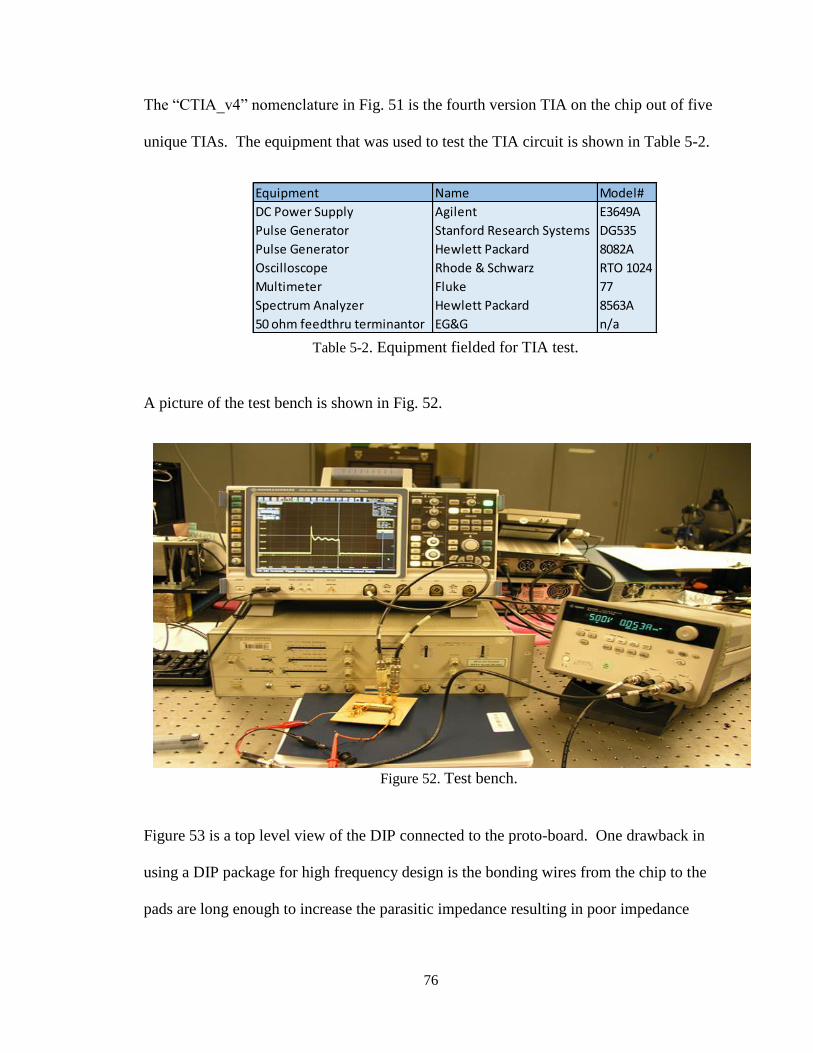
76
The “CTIA_v4” nomenclature in Fig. 51 is the fourth version TIA on the chip out of five
unique TIAs. The equipment that was used to test the TIA circuit is shown in Table 5-2.
A picture of the test bench is shown in Fig. 52.
Figure 53 is a top level view of the DIP connected to the proto-board. One drawback in
using a DIP package for high frequency design is the bonding wires from the chip to the
pads are long enough to increase the parasitic impedance resulting in poor impedance
Figure 52. Test bench.
Table 5-2. Equipment fielded for TIA test.
Equipment Name Model#
DC Power Supply Agilent E3649A
Pulse Generator Stanford Research Systems DG535
Pulse Generator Hewlett Packard 8082A
Oscilloscope Rhode & Schwarz RTO 1024
Multimeter Fluke 77
Spectrum Analyzer Hewlett Packard 8563A
50 ohm feedthru terminantor EG&G n/a

77
matching. The poor impedance control could result in the degradation of the output
response to current pulses with fast rise times (several nanoseconds).
The testing requires current-to-voltage conversion, so in order to generate a
current at the input of the TIA, a voltage source (𝑣𝑝𝑢𝑙𝑠𝑒 in Fig. 51) and an input resistance
is used. The input pulse current as a function of time is
𝑖𝑖𝑛(𝑡) =𝑣𝑝𝑢𝑙𝑠𝑒(𝑡)
𝑅𝑖𝑛 (5-8)
Throughout the testing, 𝑣𝑝𝑢𝑙𝑠𝑒 or 𝑅𝑖𝑛 were adjusted in order to produce a large enough
current. A coupling capacitor is utilized to isolate the pulse generator from the input of
the TIA. Since the pulse generator is terminated with 50 ohms, and the input impedance
of the circuit is much larger than 50 ohms, a 50 ohm feedthru is connected in between the
pulse generator and 𝑅𝑖𝑛 to reduce the reflections caused by an impedance mismatch. The
Figure 53. Top level view of DIP.

78
output of the TIA circuit is connected to an oscilloscope with 50 ohm coupling, and
therefore a 50 ohm feedthru is not needed.
Two different types of pulse generators were fielded in order to test the TIA with
input currents that have large pulse widths (>100 ns) and short pulse widths (<100 ns).
The Stanford Research Systems DG535 produced a 𝑣𝑝𝑢𝑙𝑠𝑒(𝑡) at an amplitude of −11 𝑉𝑝𝑝
with a pulse width of 800 ns, and the Hewlett Packard 8082A generated a 𝑣𝑝𝑢𝑙𝑠𝑒(𝑡) at an
amplitude of −5 𝑉𝑝𝑝 with pulse widths in the tens of nanoseconds. Both pulse generators
have the ability in generating pulses with rise times of 1 ns or more. The drawback in
fielding the 8082A pulse generator is that signal amplitudes were limited to −5 𝑉𝑝𝑝, so to
get a meaningful signal through the amplifier, the input resistor was reduced from 100 kΩ
to 10 kΩ. Figures 54 through 56 show the input pulses for the DG535 and 8082A that
were used in creating the input current pulses. All of the input voltage signals were
falling-edge pulses. As a result, the output pulses will have a rising-edge since the output
of the TIA is 180° out of phase with the input. The screen shots were taken directly from
the Rhode & Schwarz RTO 1024 oscilloscope.

79
At 5x attenuation, the actual input voltage peak-to-peak is -11 V with the DG535 pulse
generator.
Figure 55. 8082A input voltage pulse #2 at < 5ns pulsewidth.
Figure 54. DG535 input voltage pulse #1 at 5x attenuation and 844 ns pulse width.

80
Notice in Fig. 56 the same pulse generator was used, but one signal appears to behave as
a square wave, and has a pulse width of 5 ns; however, the pulse in Fig. 55 is not a square
wave, but has a pulsewidth of approximately2 ns.
The output pulses are shown in Figures 57 through 60.
Figure 56. 8082A input voltage pulse #3 at < 10ns pulsewidth.

81
Figure 58. Output pulse #2.
Figure 57. Output pulse #1.

82
Table 5-3 displays the theoretical and measured results for different input stimuli.
Figure 60. Output pulse #4.
Figure 59. Output pulse #3.

83
There are several points regarding these results that need addressing. Output pulse #1
and #2 corresponds with the Input pulse #1 generated from the DG535 and Input pulse #2
generated from the 8082A respectively. Notice that the output signal in Fig. 58 is an
order of magnitude smaller than the signal in Fig.57, but the feedback resistance for input
pulse #1 is almost five times smaller. The expectation is that even for a smaller input
pulse current with a significantly larger feedback resistor, the gain for output pulse #2
should be approximately twice as much the output pulse #1. An explanation for this
discrepancy lies with the DC output voltage. Output pulse #2 is starting close to ground
(there is a measured 7 mV offset), and with a small offset, the circuit is barely driving the
50 ohm load of the oscilloscope, and therfore there is not much gain. From the DC
sweep of the output voltage in Fig. 37, the expectation is that the minimum DC offset is
approximately 300 mV, but the actual measured DC offset is an order of magnitude
smaller. One possible reason for this occurrence is a mismatch in the devices. The
improved TIA schematic in Fig.13 is again shown in Fig .61 with a zoomed in shot of the
current mirror circuitry.
Table 5-3. TIA test theoretical and measured results.

84
The presumption is that the gate potential of M1 and M3 remain constant under normal
operating conditions. M1 and M3 are the current mirrors and they need to adjust the
current supply as the feedback resistance changes. As the feedback resistor size is
increased, for high gain, the amount of current that is fed through that resistor decreases
requiring larger changes in the output voltage. This results in the failure of the series-
shunt feedback amplifier which causes the overall design to fail. The way to simulate
this behavior in the current mirrors is to change the gate potential with one of the mirrors,
and verify what happens at the output of the series-shunt feedback amplifier. The entire
circuit with this change is shown in Fig. 62.
Figure 61. Improved TIA schematic with emphasis on the current mirror.

85
The transient analysis simulation for the output is displayed in Fig. 63.
The output DC voltage is now at 50 mV, but the decrease in gain is severe. The change
in output voltage from the DC offset is approximately 2 mV. Compare this result with
the 15 mV change in output voltage from Fig. 41. Another issue is the current mirror
Figure 63. Transient analysis results of a positive increase in the M1 gate potential.
Figure 62. Improved TIA schematic with a negative increase in the M1 gate potential.

86
sensitivity to a mismatch in MOSFETs. If the channel width of M1 is one micrometer
different then the channel width of MB1, the change in the output is drastic. The same
reasoning can easily apply to the MB3 and M3 transistors Figure 64 shows the output
voltage with a one micrometer increase in the channel width of M1, and Fig. 65 shows
the same output with a one micrometer decrease in the channel width of M1.
With a 1 μm increase in the channel length of M1 causes the DC offset at the output of
the TIA to change to 49 mV, and the gain has also been hampered. In this particular
case, the TIA is a unity-gain device.
Figure 64. Transient analysis results of a 1 μm increase in the channel width of M1.

87
Look at what happens to the TIA when M1 has a 1 μm decrease in the channel width.
Now the DC offsetvoltage is approximately 712 mV, and the maximum change in voltage
is 15 V/V. The implication is the lack of balance between the biasing and the feedback
resistor is causing the current mirrors to fight against each other, and therefore shutting
off the series-shunt feedback amplifier.
The noise measurement was taken with a Hewlett Packard 8563 Spectrum
Analyzer. Recall that in order to take a proper noise measurement for the TIA, leave the
input pin opened (Hi-Z), so that only the noise and not the desired signal is actually
measured. A picture showing the output noise of the TIA is in Fig. 66.
Figure 65. Transient analysis results of a 1 μm decrease in the channel width of M1.

88
The picture in Fig. 66 shows the horizontal axis is frequency (Hz), and the vertical axis is
in RMS voltage. A sweep of the output noise starts at 0 and ends at 10 MHz. The
resolution bandwidth for this particular measurement is 𝑓𝑟𝑒𝑠 = 2 𝑀𝐻𝑧. Figure 66 shows
the flicker noise (1/𝑓) roll off, and according to the marker, the knee frequency is at
approximately 5 MHz. The RMS voltage at the one-over-f knee frequency is 68 μV
according to the on-screen marker. To determine the output noise power spectral density,
the resolution bandwidth and the output noise RMS voltage are needed. The equation is
given by
𝑉𝑜𝑛𝑜𝑖𝑠𝑒2 (𝑓) =
𝑉𝑜𝑛𝑜𝑖𝑠𝑒,𝑅𝑀𝑆2
𝑓𝑟𝑒𝑠=
(68 𝜇𝑉)2
2 𝑀𝐻𝑧= 2.31 × 10⁻¹⁵ 𝑉2/𝐻𝑧 (5-9)
The voltage spectral density is given by
Figure 66. Spectrum analyzer output noise measurement of the improved TIA.

89
𝑉𝑜𝑙𝑡𝑎𝑔𝑒 𝑆𝑝𝑒𝑐𝑡𝑟𝑎𝑙 𝐷𝑒𝑛𝑠𝑖𝑡𝑦 = √𝑃𝑆𝐷 = √2.31 × 10⁻¹⁵ 𝑉2/𝐻𝑧 = 48.1 𝑛𝑉/√𝐻𝑧
(5-10)
The input-referred RMS noise is
𝐼𝑖𝑛𝑜𝑖𝑠𝑒,𝑅𝑀𝑆 =𝑉𝑜𝑛𝑜𝑖𝑠𝑒,𝑅𝑀𝑆
𝐴=
68 𝜇𝑉
23.1 𝑘𝛺= 2.94 𝑛𝐴 𝑅𝑀𝑆 (5-11)
This is approximately two orders-of-magnitude smaller than what was shown in equation
5-1. The reason for the discrepancy is the series-shunt feedback amplifier is essentially
turned off as a result of the feedback altering the biasing current.
5.3 TIA FINAL DESIGN
The improved TIA demonstrates the challenges involved in designing a suitable
current-to-voltage amplifier for the optical pyrometer ASIC. One reason for the lack of
robustness of the improved TIA lies with the relationship between the biasing and the
feedback network. Any redesign will have to address the issue of isolating the feedback
network effects from the DC biasing. One topology that does this is shown in Fig. 67.

90
The final TIA circuit has a number of different features that address the shortcomings
frrom the previous design. One of the problems with the improved TIA was the inability
to set the biasing current, and because the bias point was dependent on the feedback
network, not having the control over this parameter meant an asymmetrical voltage
swing. This implies that the gain of the TIA was not only dependent on the feedback
resistance, but dependent on the relationship between the feedback and bias point. Here
is how that problem was corrected. An off-chip resistor, or potentiometer will set the
bias current as seen in Fig. 67 with a pin labeled Rbias. This pin allows the user to set the
bias current, 𝐼𝑏𝑖𝑎𝑠, across the foloded-cascode current mirrors, the differential pair
amplifier, and the the series-shunt feedback amplifier. More control over the biasing in
the TIA will prevent the problems with the feedback and bias relationship. A folded-
cascode current mirror structure is utilized to better match the bias current in the PMOS
and NMOS current mirrors. The series-shunt feedback amplifier at the output is identical
Figure 67. Final TIA design for the optical pyrometer ASIC.

91
to the one used in the improved TIA; however, the ambiguity with the input voltage
signal to the series-shunt amplifier in the previous design was one of the reasons that a
failure occurred in the rest of the circuit, so understanding the bias current behavior at the
output and input is crucial in determining the success of the overall TIA. Figure 68
shows the TIA at higher level of abstraction. The transistor-level details are kept hidden.
Now that the biasing resistor is set to give the user more control of where to set
the TIA’s quiescent point, the next problem is determining the added resistance needed at
the noninverting pin of the TIA in Fig. 68. Looking back at Fig. 67, the output of the
TIA has two DC currents flowing into 50 ohm load. The total current suuming at the
output node is
𝐼𝑂,𝐷𝐶 = 𝐼𝑏𝑖𝑎𝑠 + 8 ∙ 𝐼𝑏𝑖𝑎𝑠 (5-11)
Figure 68. Final TIA op-amp schematic.

92
Figure 67 shows that the PMOS device connected at the output via the drain terminal has
eight times the width, and therefore will have approximately eight time the bias current.
If the DC output current is driving a 50 ohm load, or oscilloscope, then the offset voltage
becomes
𝑉𝑜𝑓𝑓𝑠𝑒𝑡 = 9𝐼𝑏𝑖𝑎𝑠 ∙ 50 = 450 ∙ 𝐼𝑏𝑖𝑎𝑠 (5-12)
To balance this DC voltage at the output of the TIA, the input pin of the TIA also needs
to have an equivalent 𝑉𝑜𝑓𝑓𝑠𝑒𝑡, so if a 450 Ω resistor is placed on the noninverting to
ground, then another 𝑉𝑜𝑓𝑓𝑠𝑒𝑡 appears on that pin, and therefore the offset voltage also
appears on the input pin. Since the potential difference between the noninverting pin and
the output are identical, no DC current will flow through the feeback resistance, and
therefore the relationship between the feedback and biasing are no longer intertwined.
Figure 69 is the schematic and DC analysis of the output voltage versus input
current respectively. This will aid in demonstrating where the amplifier is operating, and
the amount of gain that is expected.

93
Clearly with only 1 μA of peak current through the TIA with a 5 kΩ bias resistor
and 100 kΩ feedback resistance, there is expectation of large gain. A peak input current
pulse of 5 μA with a 100 kΩ feedback resistor will give approximately 100 kΩ of gain
according to Fig. 70.
Figure 70. Final TIA DC analysis gain expectation with an 𝑅𝑏𝑖𝑎𝑠 = 5𝑘𝛺.
Figure 69. Final TIA DC analysis schematic.

94
Increasing the 𝑅𝑏𝑖𝑎𝑠 resistance will improve the performance of the TIA. Figure 71
shows the transient analysis results for an 𝑅𝑏𝑖𝑎𝑠 = 5 𝑘𝛺.
Clearly with a larger bias resistance the response and gain improves. Figure 72 is a plot
of the output voltage with an 𝑅𝑏𝑖𝑎𝑠 = 20 𝑘𝛺.
Notice that the output voltage has an undershoot. Now what is happening to the TIA as
the current source is providing too much current to the amplifiers is the TIA is at the edge
of instability. At this point, the TIA is marginally stable, and any increase in the current
Figure 72. Final TIA transient analysis with an 𝑅𝑏𝑖𝑎𝑠 = 20 𝑘𝛺.
Figure 71. Final TIA transient analysis with an 𝑅𝑏𝑖𝑎𝑠 = 5 𝑘𝛺.

95
will force it into an unstable state. Figure 73 shows a transient analysis with a feedback
resistance of 25 kΩ, and an 𝑅𝑏𝑖𝑎𝑠 = 2 𝑘𝛺. This demonstrates a fast pulse response.
Figure 74 is a plot of the final TIA closed-loop gain with a feedback resistance of 100
kΩ.
For this TIA, the unity-gain bandwith occurs at approximately 2.5 GHz. A plot of the
output noise power spectral density is in Fig. 75.
Figure 74. Final TIA closed-loop gain with an 𝑅𝑓 = 100 𝑘𝛺.
Figure 73. Final TIA transient analysis with an 𝑅𝑏𝑖𝑎𝑠 = 2 𝑘𝛺, and 𝑅𝑓 = 25 𝑘𝛺.

96
The RMS output noise voltage is 4.7 mV, so the input-referred noise RMS current is
𝐼𝑖𝑛𝑜𝑖𝑠𝑒,𝑅𝑀𝑆 =𝑉𝑜𝑛𝑜𝑖𝑠𝑒,𝑅𝑀𝑆
𝐴𝐶𝐿=
4.7 𝑚𝑉
95 𝑘𝛺≈ 50 𝑛𝐴 𝑅𝑀𝑆 (5-13)
5.4 TRANSIMPEDANCE AMPLIFIER LAYOUT
The key element in the design of the optical pyrometer ASIC is the design of the
transimpedance amplifier (TIA). Chapters 3 discussed two different types of TIAs, one
that was referred to as a generic TIA, and the other called an improved TIA. The
improved TIA addressed the shortcomings with the open-loop gain of the generic model;
however, the improved TIA was sensitive to any mismatch in the biasing circuitry, so that
design is not suitable for the optical pyrometer ASIC. The end of Chapter 5 discusses a
viable option for a practical TIA. Figure 76 is the layout of the final TIA, and Fig. 76 is
the 1.5 𝑚𝑚 × 1.5 𝑚𝑚 chip layout which included 4 TIAs.
Figure 75. Final TIA output noise PSD with an 𝑅𝑓 = 100 𝑘𝛺.

97
The chip in Fig. 77 consists of four TIAs. Two of the TIA have a 450 Ω bias resistor on
chip while the other two require external bias resistors. The chips are fabricated with a
C5 Process (On Semiconductor 500 nm) with two polysilicon layers and 3 metal layers.
Figure 77. Chip layout 1.5 𝑚𝑚 × 1.5 𝑚𝑚.
Figure 76. Layout of the final TIA.

98
CHAPTER 6 – CONCLUSIONS AND FUTURE WORK
The infrared optical pyrometer ASIC will consist of a 16 channel linear
photodiode array and a folded-cascode differential TIA with a gain of 100 kΩ, a
bandwidth of 30 MHz, and an input-referred noise current of 50 nA RMS. Two different
topologies were designed an analyzed, but ultimately the only viable option is the Final
TIA circuit. The key element in the Final TIA design was the use of a techique called
replicatitive biasing to ensure minimal DC leakage through the feedback network. Once
a relationship was identified between the biasing and feedback, the Final TIA appeared to
be a more practical consideration. The simulations have shown promise, and the chip is
to be fabricated in November of 2013. The anticipated testing date is the middle of
December.
Future work also includes investigating ways to further reduce noise while
improving bandwidth, and also requires extensive testing of the final TIA prior to its
implementation within the optical pyrometer ASIC. The chip design gives us the ability
to test the performance of each TIA for several different scenarios simultaneously.
Testing will require the in-house fabrication of a PCB that will include a 16 photodiode
linear, the TIA chip, and high frequency 50 ohm SMA connectors that connect directly to
16 channels of an off-chip digitizer. The PCB will route the power, off-chip bias resistor,
feedback resistor, and I/O signals of the TIA chip. This setup will make the testing of
four TIAs easier while at the same time minimizing the effects of parasitics from
protoboarding. In future generations of the infrared optical pyrometer ASIC, the
reduction in TIA power will be essential in minimizing the thermal load on the
photodiode array. One drawback in using the Final TIA over the Improved TIA is the

99
significant power draw of the Final TIA. Going from a single-ended input amplifier to a
differential amplifier implies an increase in the dissipated power. One way to potentially
reduce the thermal load on the photodiodes is to mulltiplex the PD signals onto a single
TIA chip. An ADC is another option as an add-on to the optical pyrometer by acting as
an on-board digitizer thereby completing the first prototype chip to be fileded in the next
shock physics experiment.

100
REFERENCES
[1] Shock Physics. (n.d.). Shock Physics. Retrieved November 4, 2013, from
https://www.llnl.gov/str/Holmes.html.
[2] The Limits of Technology. (n.d.). The Limits of Technology. Retrieved November
4, 2013, from http://www.ibm.com/developerworks/rational/library/2082.html.
[3] Saleh, B., & Teich, M. (2007). Semiconductor photon detectors. Fundamentals of
Photonics (2 ed., pp. 762-767). Hoboken: John Wiley & Sons.
[4] Hui, R., & O'Sullivan, M. (2009). Photodetectors. Fiber Optic Measurement
Techniques (pp. 32-43). Burlington: Elsevier Academic Press.
[5] Kasap, S. O. (2001). Photodetectors. Optoelectronics and Photonics Principles
and Practices (pp. 217-246). Upper Saddle River: Prentice Hall.
[6] Pierret, R. (1996). Pn-Junction Diodes. Semiconductor Device Fundamentals (pp.
349-356). Reading: Addison-Wesley.
[7] Węgrzecka*, Węgrzecki, M., Grynglas, M., Bar, J., Uszyński, A., Grodecki, R., et
al. (2004). Design and properties of silicon avalanche photodiodes. Opto-
Electronics Review, 12(1), 95-104.
[8] Baker, R. J. (2010). Feedback Amplifiers. CMOS: circuit design, layout, and
simulation (3rd ed., pp. 1099-1145). Piscataway, NJ: IEEE Press.
[9] Neamen, D. A. (2007). Feedback and Stability. Microelectronics: circuit analysis
and design (3rd ed., pp. 847-923). New York: McGraw-Hill.
[10] Razavi, B. (2001). Feedback. Design of analog CMOS integrated circuits (pp.
246-284). Boston, MA: McGraw-Hill.

101
[11] Säckinger, E., & Guggenbühl, W. (1990). A High-Swing, High-Impedance MOS
Cascode Circuit. IEEE Journal of Solid-State Circuits, 25, 289-298.
[12] Bakshi, U., & Godse, A. P. (2009). Feedback Amplifiers. Analog Electronics (pp.
1-50). Shaniwar Peth: Technical Publications Pune.
[13] Sansen, W. M. (2006). Feedback voltage and transconductance amplifiers. Analog
design essentials (pp. 363-388). New York: Springer.
[14] Motchenbacher, C. D., & Connelly, J. A. (1993). Low-Noise Electronic System
Design. New York: John Wiley & Sons.
[15] Mancini, R., & Carter, B. (2009). Op Amp Noise Theory and Applications. Op
amps for everyone (3rd ed., pp. 163-188). Amsterdam: Newnes/Elsevier.
[16] Yuen, H., & Chan, V. (1983). Noise in homodyne and heterodyne detection.
Optics Letters, 8(3), 177-179.
[17] Feldman, R., & Valdez-Flores, C. (2010). Important Distributions. Applied
Probability and Stochastic Processes (2. ed., pp. 15-16). New York: Springer.
[18] Kogan, S. (1996). 1/f noise and random telegraph noise. Electronic noise and
fluctuations in solids (p. 206). Cambridge [England: Cambridge University Press.
[19] Chang, J., Abidi, A. A., & Viswanathan, C. R. (1994). Flicker Noise in CMOS
Transistors from Subthreshold to Strong Inversion at Various Temperatures. IEEE
Transactions on Electron Devices, 41(11), 1965-1971.

102
VITA
Graduate College
University of Nevada, Las Vegas
Jared Gordon
Degree:
Bachelor of Science, Electrical Engineering (Cum Laude), 2009
University of Nevada, Las Vegas
Employment:
National Security Technologies (NSTec), 2010
Thesis Title: Design and Fabrication of an Infrared Optical Pyrometer ASIC as a
Diagnostic for Shock Physics Experiments
Thesis Examination Committee:
Chairperson, R. Jacob Baker, Ph. D.
Committee Member, Peter Stubberud, Ph. D.
Committee Member, Rama Venkat, Ph. D.
Committee Member, Evangelo Yfantis, Ph. D.