DESIGN AND ANALYSIS OF STANDALONE PV SYSTEM · future. PV systems are widely used for generating...
38
DESIGN AND ANALYSIS OF STANDALONE PV SYSTEM A thesis submitted in partial fulfilment of the requirements for the award of the degree of Bachelor of Technology in “Electrical Engineering” By Chinmay Garanayak (111EE0033) Bipin Bihari Behera (111EE0195) Under the supervision of Prof. Somnath Maity Department of Electrical Engineering National Institute Of Technology, Rourkela Rourkela – 769008, Odisha
Transcript of DESIGN AND ANALYSIS OF STANDALONE PV SYSTEM · future. PV systems are widely used for generating...

DESIGN AND ANALYSIS
OF
STANDALONE PV SYSTEM
A thesis submitted in partial fulfilment of the requirements for the award of
the degree of
Bachelor of Technology in “Electrical Engineering”
By
Chinmay Garanayak (111EE0033)
Bipin Bihari Behera (111EE0195)
Under the supervision of
Prof. Somnath Maity
Department of Electrical Engineering
National Institute Of Technology, Rourkela
Rourkela – 769008, Odisha

2
DEPARTMENT OF ELECTRICAL ENGINEERING
NATIONAL INSTITUTE OF TECHNOLOGY, ROURKELA
CERTIFICATE
This is to certify that the thesis entitled ―Design and analysis of Standalone PV System‖,
submitted by Chinmay Garanayak, Roll no. 111EE0033 and Bipin Bihari Behera, Roll no.
111EE0195, in partial fulfilment of the requirements for the award of Bachelor of Technology
in Electrical Engineering at National Institute of Technology, Rourkela. A bonafied record
of research work carried out by them under my supervision and guidance. The candidates have
fulfilled all the prescribed requirements. To the best of my knowledge and belief, the reports
and results embodied in this thesis have not been submitted elsewhere for a degree or diploma.
In my opinion, the thesis is of the required standard for the award of a degree in Bachelor of
Technology in Electrical Engineering.
Place: Rourkela Prof. Somnath Maity
Date: 11 May 2015 Dept. of Electrical Engineering
NIT, Rourkela

3
ACKNOWLEDGEMENTS
We would like to express our indebtedness and deepest gratitude to our supervisor
Prof. Somnath Maity, Dept. of electrical Engineering, NIT Rourkela, for his guidance,
motivations, immense knowledge and extended confidence at every step due to which it is
possible for us to complete the work in the stipulated time. We also thank him for his valuable
suggestions and insightful comments which inspired us to explore more information regarding
the project. We also express our indebtedness to all Faculty and staff of Dept. of Electrical
Engineering for their support by establishing a working environment. Finally we would also
like to acknowledge our friends for their suggestions and cooperation at various steps while
completing this thesis.
Chinmay Garanayak
Bipin Bihari Behera
Dept. of Electrical Engineering
NIT Rourkela

4
CONTENTS
Abstract 5
List of Figures 6
List of Tables 7
1. Introduction 8
2. Literature survey 9
3. PV System 11
3.1. Solar Energy 11
3.2. Photovoltaic cell 11
3.3. Working Principle 12
4. Maximum Power Point Tracking 14
4.1 MPPT Techniques 14
4.1.1. Control system with current or voltage reference 15
4.1.2. Incremental Conductance Method 15
4.1.3. Perturb and Observe Method 15
4.2 MPPT Algorithm 16
5. DC – DC Converter 17
5.1 Working Principle 17
5.2 Simulink model and results 18
6. Inverter 20
6.1 Modelling of output voltage controller 22
6.2 Compact form expression for the exact switched model 23
6.3 Transferring the model into small signal averaged model 23
6.4 Effect of variation of different parameters upon inverter 26
6.5 Inverter model and results 28
7. Simulink model of PV system 32
7.1 Results 32
8. H – Bridge Inverter IC 34
8.1 Features 34
8.2 Pin configuration 35
9. Conclusion 37
10. References 38

5
ABSTRACT
Most of the energy sources originate from tried and conventional sources like fossil fuels, for
example, coal, natural gasses and crude oil. Then comes the hydro power systems. These
powers are frequently termed as non-renewable energy sources. But generation of hydro power
requires water storage systems. As the conventional energy sources are present in limited
amount generation of renewable energy sources like solar, tidal etc. is a great necessity of these
days.
In this project we have modelled the standalone voltage source inverter first by using a DC
source as input power and then instead of using direct DC source, a PV system is connected as
input source and the output of the inverter is studied and analyzed. The unregulated DC output
supply of the PV array is mainly because of changes in weather conditions. The maximum
power is tracked with respect to irradiance levels and temperature by the help of DC-DC
converter. The AC output voltage and frequency are regulated. Sinusoid pulse width
modulation (SPWM) technique is implemented for voltage control for inverter and it is a
closed loop control. For the design of inverter, its state space model is formulated and effects of
various parameters like load resistance, controller gain and time constant is analyzed.

6
LIST OF FIGURES
Figure No. Name of Figure Page No.
1.1 Schematic diagram of standalone PV system 8
3.1 Basic constructional features of PV cell 11
3.2 Equivalent circuit of PV module 12
4.1 Typical I – V characteristics 14
4.2 Typical P – V characteristics 14
5.1 Boost converter circuit 17
5.2 Simulink PV module with converter 18
5.3 Output of PV array 19
5.4 Converter output 19
6.1 Inverter circuit diagram and signal of PWM modulator 21
6.2 Bode plot for different resistance value 26
6.3 Bode plot for different kv 27
6.4 Bode plot for different tv 27
6.5 Inverter Simulink block diagram 28
6.6 Reference signal 29
6.7 Carrier signal 29
6.8 Output voltage of inverter 29
6.9 Output current of inverter 30
6.10 Plot of state variables 30
6.11 FFT analysis of voltage waveform 31
6.12 FFT analysis of current waveform 31
7.1 PV system in Simulink 32
7.2 Converter output voltage when connected to inverter 32
7.3 Control voltage 32
7.4 Output voltage 33
7.5 Output current 33
8.1 Pin configuration of 33887 IC 35

7
LIST OF TABLES
Table No. Name of Table Page No.
6.1 Parameters used in simulation 25
6.2 Variation of GM, PM, GF, PF with load resistance 26
6.3 Variation of GM, PM, GF, PF with kv 27
6.4 Variation of GM, PM, GF, PF with tv 28
8.1 33887 Pin Definitions 35

8
1. INTRODUCTION
Renewable energy source are immense necessity in present as well as in future. Among various
renewable energy systems, most important role is played by PV systems i.e. photovoltaic
power generation systems as a clean power source to cope with the electricity demands in
future. PV systems are widely used for generating power from solar energy. Of all renewable
energy systems, PV based systems are the most eco-friendly energy solution for generating
power. A schematic representation on PV system is shown in Fig.1.1.
The power delivered by the PV system is dependent on the radiance of solar energy and that
vary time to time. So, the voltage and current and hence power delivered by the system is a
variable quantity. To obtain maximum efficiency the maximum power point is tracked by
applying an MPPT algorithm. The converter is used to obtain a constant output DC voltage
which can be fed to an inverter to obtain alternating voltage which can be fed to a grid to meet
the power demand of society.
But the output of a VSI is not a nice sinusoidal wave rather it is a square wave and we know
from Fourier analysis square wave is the combination of sine waves of fundamental frequency
its higher order harmonics. Before feeding to grid the harmonic components must be reduced
which can be done by using SPWM for switching the MOSFETS or IGBTS used for switching
and using inductive filter because high frequency switching techniques decreases lower order
harmonics but increases higher order harmonics.
Fig. 1.1 Schematic diagram of standalone PV system

9
2. LITERATURE SURVEY:
Renewable sources of energy are also known as non-conventional type of energy. These
sources can be replenished by naturally occurring processes. Examples of renewable energy
sources are solar energy, geo thermal energy, bio-energy-bio-fuel, hydropower and wind
energy etc. Sun and wind are bulk amount of renewable energy sources. In a PV system the
light and heat energy that is available to us from sun is converted to electrical energy by the use
of semiconductor material junctions.
World’s leading economies have installed solar PV systems to produce power in range of MW.
Solar PV systems can be availed in variety of sizes for various applications and are made up of
semiconductor wafers. Solar cells combined to form solar arrays which can be regarded as the
basic building block of PV system. As the efficiency of solar cells are very less power
electronic components are used with it to harvest maximum efficiency. They can be installed
on ground or on roof. Roof top installations offer good results if we are concerned about energy
saving.
The tremendous potential associated with PV system is known over the years. Log Cabin
Systems (LCS) and Urban Home Systems (UHS) are variety of technical arrangements
(Dumais, 2010). In earlier days MI (micro-inverter) were basically multistage configured. A
team of researchers in year 1996 presented an integrated power processing system with PV and
it is called as an AC module. The power rating was 250 W. Following them, Kusakawa in 1998
introduced the concept of transformer less MI. Two staged inverter was designed by them and
the inverter was directly connected to the PV module followed by a buck/boost converter. Low
input voltage is provided by them to the switching devices; So MOSFETs are used with low
conduction losses. The inverter Conduction losses are reduced and the efficiency is increased
by the designing of a two stage MI which is based on Zero Voltage Switching inverter by M.
Andersen and T.B. Alvesten in 1995. In 2008, a multilevel topology of inverter was proposed
which does not inject DC to the grid. The methods of control using a two stage transformer less
system are proposed by Franke et al. (2010) and they adopted a three phase H bridge inverter
for interconnecting grids. A useful conclusion is drawn by his work i.e. the losses caused by
current control PWM is less than the PI controller. But due to variance in switching frequency,
the power quality reduces. A two stage micro inverter based on push pull converter with a
single phase bridge inverter was designed by Trujillo et al. (2010, 2011). The bridge topology
was not followed and switch numbers is reduced to two but they bear extra voltage which

10
results in requirement of higher rating. Thus control circuitry became simpler. Control scheme
was prepared for a MI. In this scheme, MI worked as a current source and it operates as a
voltage source for island mode.
Now-a-days the PV system is used in also hybrid energy systems with the tidal and wind
energy systems. Because the load demand can be fulfilled at the time of need by all these
systems if one system is not able to provide the required amount of load. The sun light is not
available all the time and other energy sources are not available all the time, so these systems
can be complementary to each other and if more amount of energy is available at a time we can
save this in the form of chemical energy in batteries.
The solar cells can be modelled mathematically with the help of a current source with a parallel
diode and a resistor in series and parallel to it. DC link capacitor is connected with it to
maintain the voltage nearly constant and it can be connected with the boost converter which
can be controlled by MPPT algorithm to track maximum power from the converter. The
converter voltage is turned in to alternating by the use of an inverter.

11
3. PV SYSTEM
3.1 Solar energy
Solar energy is the most readily available form of energy. The radiant light from the sun
and the heat is harnessed using technologies like photovoltaic, solar heating, thermal energy,
artificial photosynthesis, etc. It is the most important of the non-conventional sources of energy
and depending on the way they convert it into solar power, its technologies are characterized as
either active or passive. Use of concentrated solar power, photovoltaic systems and solar water
heating are included in active solar techniques whereas orienting a building to the sun is
included in Passive techniques to harness the energy.
There are huge benefits in developing inexhaustible, affordable and clean solar energy
technologies. Solar energy as an inexhaustible, indigenous and mostly import-independent
resource has several advantages. These include enhanced sustainability, reduced pollution,
lowered the costs of mitigating global warming and fossil fuels.
3.2 Photovoltaic cell
Generation of photovoltaic power involves the technology which converts thermal radiation
from the sun directly into electricity through units called photovoltaic cells / solar cells. PV
cells are usually made up of semiconductor materials with differently doped mono-crystalline
as well as poly-crystalline silicon layer forming a pn junction. Thus a solar cell is nothing but a
diode with a large surface area and a large area of pn junction. A basic cell configuration is
shown in Fig.3.1.
FIG.3.1 Basic constructional features of PV cell.

12
The load is connected to the cell through the metallic contacts. To enhance the absorption of
radiation by reducing reflection, an antireflection coating of SiO2 is applied on the top surface.
For mechanical protection, the cell is placed under a glass cover and attached to it by a
transparent adhesive. A single silicon solar cell with efficiency values between 15 – 18 %
develops an open circuit voltage of the order of 0.65 V and generates a maximum current
density between 35 – 40 mA / cm2.
In a PV system, single solar cells are combined in series – parallel arrangement to form a PV
Module, and several modules in series – parallel make a solar array.
3.3 Working principle
PV cell works on the principle of photoelectric effect which is defined as a phenomenon where
sunlight of certain wavelength is absorbed by a matter leading to ejection of an electron from
its conduction band. In PV cell, when light is absorbed by the pn junction, the energy of the
absorbed photon is transferred to the electron system of the material. These results in the
charge carrier generation which are separated at the junction. Theses carriers at the junction
region are electron-hole pairs, which creates a potential gradient, gets accelerated under the
effect of electric field and circulate as the current through an external circuit. The product of
square of current with the circuit resistance gives the power which is converted into electricity.
The rest power of the photons raises the cell temperature.
Fig. 3.2 Equivalent circuit of PV module
Vo
+
-
Sunlight

13
The equivalent circuit shown in Fig. 3.2 describes the physics behind PV cell. The circuit
behaviour determines the output characteristics of PV cell. The effect of forward biasing of the
pn junction is represented by the diode. The output current is given by
[ (
) ]
Where
Vo = voltage appearing across diode.
V = load voltage.
IL = photo generated current.
Rs = internal (series) resistance of the system.
Rsh = shunt resistance
Io = reverse saturation current of the diode.
T = Temperature in kelvin.
n = Ideality factor (≈1.92).
K = Boltzmann constant (1.38 x 10⁻²³
J / K).
q = electronic charge (1.6 x 10⁻¹⁹
C).
When the is open circuited, i.e., when I = 0, the voltage Vo across the shunt branch appears as
the open circuit voltage Voc across the output terminals. Neglecting the effect of Rsh, the open
circuit terminal voltage can be written as
(
)

14
4. MAXIMUM POWER POINT TRACKING
There is a poor overall efficiency when solar energy is converted into usable electrical energy
using the PV system. Maximum power point tracking (MPPT) is a technique that is used to
extract the maximum possible power from one or more photovoltaic modules and thus it
increases the efficiency of the system. The relationship between solar irradiance, resistance and
temperature produce a non-linear output. This relationship can be analyzed by the I-V curve.
Due to the nature of the I-V characteristic, for a given solar insolation level and cell
temperature, the output power is maximized at a specific load. The main purpose of the
MPPT system is sampling the output of the PV cells for any given environmental condition.
Proper resistance (load) is applied to obtain maximum power. MPPT devices are usually
integrated into a converter system which provides voltage conversion or current conversion.
They also help in regulation and filtering operation for various loads. The load may include
power grids or batteries or motor drives. Fig 4.1 and Fig 4.2 shows the typical I-V
characteristics and P-V characteristics of PV module respectively.
4.1. MPPT Techniques.
Maximum power point can be tracked using different techniques. Accuracy, simplicity,
adaptability to temperature, adaptability to irradiance variation, relative implementation cost
and control circuit complexity are some factors which determines their merits and limitations.
Some techniques are explained as follows:
Fig. 4.1 Typical I-V characteristics Fig. 4.2 Typical P-V characteristics

15
4.1.1 Control system with Voltage or Current reference.
In this method, a reference signal corresponding to maximum power point is used to compare
the actual output voltage or current of the PV array. A PI controller is used for processing the
error and its output is used for controlling the duty cycle of the PWM control signal which is
further used for the dc-dc converter. In general, the maximum power point voltage is found to
be 78% of the open circuit voltage. The corresponding current for maximum power point is
around 90% of the short circuit current. The control loop can also use these values as reference.
4.1.2 Incremental conductance method.
This method shows that; at the maximum power point on the P-V curve, rate of change in
power with respect to voltage is zero, i.e. dP / dV = 0. It can be also said that power is nearly
constant with change in voltage. As P = VI gives the output power, it can be concluded that
The instantaneous conductance of the solar panel is represented in the left hand side. When
instantaneous conductance becomes equal to the conductance of the solar cell then maximum
power point is reached. There is elimination of the error occurring due to change in irradiance
as both the current and voltage are sensed simultaneously. In this case, the complexity and the
cost of implementation increases.
4.1.3. Perturb and Observe method.
The most commonly used MPPT technique is the Perturb and Observe method because of its
ease of implementation. In this method, the voltage is increased as long as we get more power,
i.e. the operating voltage is increased till dP / dV is positive. The operating voltage is decreased
when dP / dV is negative. The voltage is kept constant if dP/ dV is near to zero within a
limit. This algorithm has a very less time complexity. It doesn’t stop on reaching very close to
the MPP, and keeps on perturbing.

16
START
4.2. MPPT Algorithm used - Perturb and Observe method.
Measure: V (t1), I (t1)
Vref = V (t1)
P (t1) = V (t1) x I (t1)
Measure: V (t2), I (t2)
Vref = V (t2)
P (t2) = V (t2) x I (t2)
∆P (t2) = P (t2) - P (t1)
∆P (t2) > 0
Vref (t3) = Vref (t2) - D Vref (t3) = Vref (t2) + D
D
17
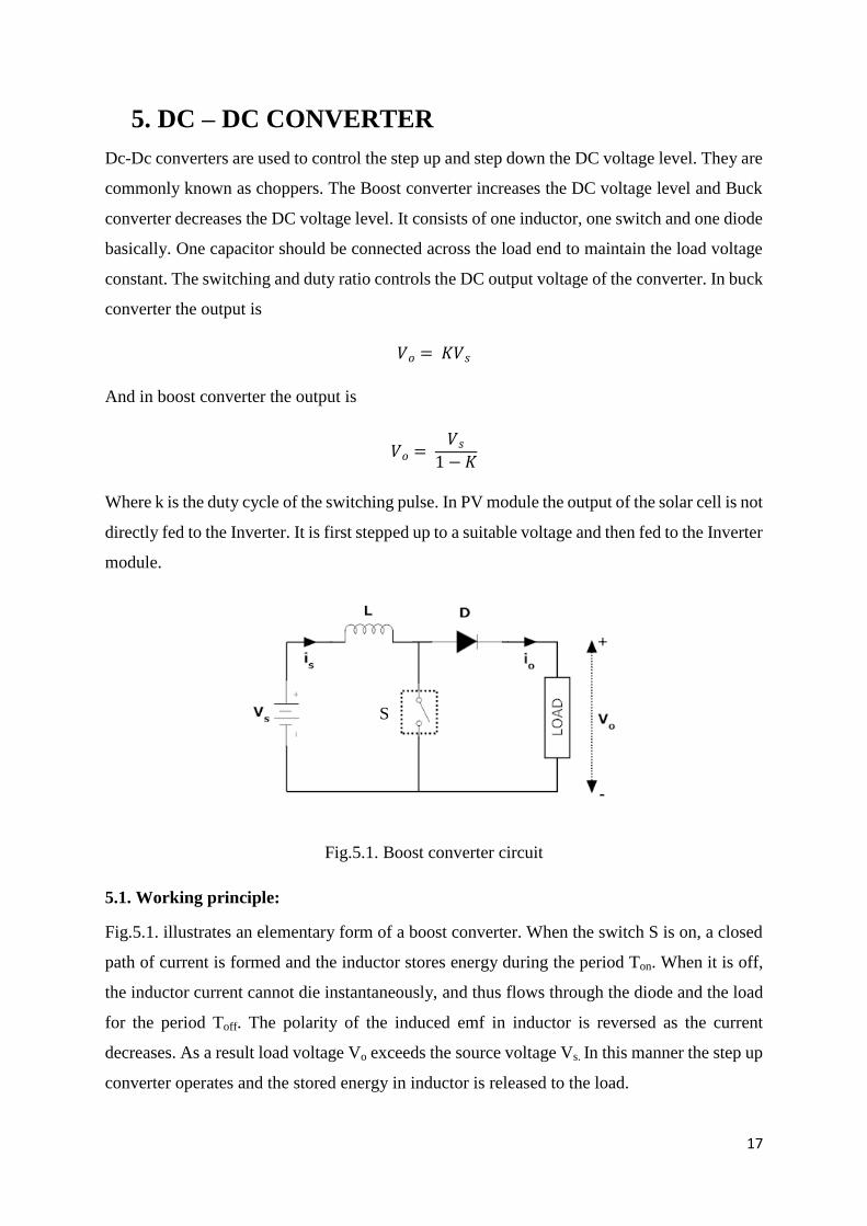
5. DC – DC CONVERTER
Dc-Dc converters are used to control the step up and step down the DC voltage level. They are
commonly known as choppers. The Boost converter increases the DC voltage level and Buck
converter decreases the DC voltage level. It consists of one inductor, one switch and one diode
basically. One capacitor should be connected across the load end to maintain the load voltage
constant. The switching and duty ratio controls the DC output voltage of the converter. In buck
converter the output is
And in boost converter the output is
Where k is the duty cycle of the switching pulse. In PV module the output of the solar cell is not
directly fed to the Inverter. It is first stepped up to a suitable voltage and then fed to the Inverter
module.
Fig.5.1. Boost converter circuit
5.1. Working principle:
Fig.5.1. illustrates an elementary form of a boost converter. When the switch S is on, a closed
path of current is formed and the inductor stores energy during the period Ton. When it is off,
the inductor current cannot die instantaneously, and thus flows through the diode and the load
for the period Toff. The polarity of the induced emf in inductor is reversed as the current
decreases. As a result load voltage Vo exceeds the source voltage Vs. In this manner the step up
converter operates and the stored energy in inductor is released to the load.
S

18
During Ton, and ; where VL = voltage across inductor and Vo = load voltage.
During Toff,
The average output voltage across the load is given by
, where the duty cycle
5.2. Simulink model and Results.
Fig. 5.2. Simulink PV module with converter
Parameters:
C1 = 0.1 µF; L = 140 mH; C2 = 1000 µF; R = 20 Ω

19
Output:
Fig 5.3 output of PV array
Fig. 5.4 converter output.
In the fig.5.3 the output of PV array with respect to time is shown when the solar irradiance is
1000 W / m2. The output voltage obtained is nearly 17 V. This voltage is stepped up to 35 V
using the boost converter. The converter output with respect to time is shown in fig.5.4.
0 0.02 0.04 0.06 0.08 0.1 0.12 0.14 0.160
5
10
15
20
25Output Voltage of PV cells vs Time
Time(in sec)
Vo
lta
ge
(in
vo
lts)
0 0.02 0.04 0.06 0.08 0.1 0.12 0.14 0.160
5
10
15
20
25
30
35
Time(in sec)
Vo
lta
ge
(in
vo
lts)
Converter output voltage vrs Time

20
6. INVERTER
A full bridge inverter as shown in Fig.6.1 Consists of four switches (MOSFET). When switch
S1, S4 conduct, load voltage becomes equal to source voltage. When switch S2, S3 conduct
voltage across load is negative of source voltage. When the inverter operates it should always
be ensured that the two MOSFETs in the same branch do not conduct simultaneously because
this would result to a direct short circuit of the source which will cause high current through
source. For resistive load, load current and load voltage are always in phase with each other.
For inductive loads, load current will not be in phase with the load voltage and the diodes
which are connected in antiparallel with MOSFETs will allow the flow of current to at the
instance when the main MOSFETs are turned off. These diodes are called feedback diodes. So
in case of resistive loads the current waveform will follow voltage wave form but if purely
inductive loads are used the waveform will be triangular in nature.
In sinusoidal pulse modulation (SPWM), in each half cycle several pulses are used. The pulse
width is determined by a sinusoidal function of the angular position of the pulse in a cycle. For
the realization of SPWM, sinusoidal reference wave is compared with a high frequency
triangular carrier wave. Both the waves are fed to a comparator. The comparator output is high,
only when the sinusoidal wave has magnitude higher than the triangular wave, otherwise it is
low. The trigger pulse generator processes the output of comparator in such a way that the
output voltages of the inverter have a pulse width in accordance to the output pulse width of the
comparator.
Modulation index (MI) in this case is defined by the ratio of Vr / Vc and the harmonic content of
the output wave is controlled by it. Here Vr and Vc represents the magnitude of reference and
carrier signal respectively. The control of output voltage is done by varying the MI.
.

21
Fig. 6.1 Inverter. (a) Circuit diagram. (b) Representative signal of the PWM modulator.
The above Fig.6.1 shows the schematic diagram of a DC-AC inverter. The switches are
activated as follows, switch S1 and S4 are driven simultaneously while switch S2 and S3 are
switched on in alternate fashion to switch S1 and S4. To sense the output voltage, a voltmeter
or a voltage sensor is there and the error in voltage is represented by the voltage difference
Vref – Vo. This error is processed using a voltage controller which is in form of a low-pass filter
or dominant pole. Vcon is the output of the controller, which is then connected to the
non-inverting input of the comparator. Here the inverting input is applied to saw tooth ramp
generator, in such a way that in steady state the switches S1 and S4 are activated at each
switching cycle while they are turned OFF when the ramp voltage Vramp (t) crosses the control
signal Vcon (t). Waveforms of state variables are periodic and are obtained by analyzing the
circuit. Here the steady state dynamics is characterized by two periods namely: the reference
voltage period Tr and the switching period Ts. Therefore the stationary periodic attractor is
settled into a two dimensional torus which is characterized by two periods, which are the line
reference period and the switching period.

22
During first phase when S1 and S4 are closed, the state equations for voltage and current are
given by
( )
During second phase when S1 and S4 are open, the state equations are as follows:
( )
Where L denotes the inductance, R is load resistance, C is capacitance of the capacitor, IL
denotes the inductor current, Vc is the output capacitor voltage and Vin is the input voltage.
6.1. Modelling of output voltage controller:
To track the output voltage Vc, a desired sinusoidal reference voltage ( ) is
used. We have used an outer voltage loop controller which is in the form of a dominant pole
(low pass-filter). As it is a low pass filter higher order frequencies and noise can be filtered by
it. To obtain less ripple in the feedback control voltage the design parameter crossover
frequency fv=1/tv is adjusted suitably together with other parameters. In frequency domain, the
small signal transfer function for this controller can be represented as:
( ) ( )
( )
Here
kv is the DC gain of the filter which is also known as velocity error constant. Another state
variable for the system defined by this dynamic controller whose dynamic behaviour is given
by:
( ( ))

23
6.2. Compact expression for the exact switched model:
The system model which is switched can be written as:
( ) During phase 1
( ) During phase 2
The system matrices and system vectors are given as:
A =
[
]
; B1 (t) =
[
( )]
; B2 (t) =
[
( )]
The switching decision is taken into account and it is considered that control signal can take
values from the set [0, 1]. Now the system switched model of the system can be expressed as
( ( ) ( )) *
( ( ))
+ ( )
Which is actually a nonlinear model and hard to solve by conventional methods.
6.3. Transferring the model into small signal averaged model:
A discontinuous switched vector filed is represented by the above equation. The discontinuous
signal u(t) which drives the system makes it the system nonlinear. To solve this type of
nonlinear equations basically two different types of methods are there. One traditional
approach is to study its dynamical behaviour by solving the discontinuous equation
numerically and then simulating the system behaviour for different parametric values under
various operating points.
But this method is disadvantageous being computationally intensive. It will take a lot of time to
solve it and it will consume more memory. Second approach is to take the average of the
system equation over a switching period which will remove the discontinuity which is caused
due to the switching action.
This can be simplified further. The reference signal can be considered to be constant and its
RMS value is used to replace it. This way, the slow-scale dynamical behaviour can be
concluded and can be drawn obtaining the small signal transfer function.

24
For our system the switched signal u (t) is replaced by its average over the duty cycle, and
hence the averaged model which is continuous is obtained and is given by
( ( ) ( ))
( ( )
) ( )
Where Vu = 1v and Vl = -1v
Now the new linear time varying model is:
[
]
[
(
)
]
[
] [
]
This model is solved in MATLAB and the output is observed. To see the effects due to the
change of different parameters i.e. load resistance, gain kv and tv the small signal transfer
function is obtained and i.e. given by:
( ) ( )
( )
( )( )(
)
Here
√ and
√
The gain margin and phase margin of the system can be obtained from the bode plot for
different values of load resistance, gain kv and time constant tv.We can take 12, 24, 36, 48, 110,
125 and 250 V as nominal input values for DC to AC inverters. We have used voltage Vin = 36
in this project an input.
To design DC to AC there are other important output specifications to be considered which are
maximum voltage, maximum power, maximum steady-state current and frequency range. In
the function of the application, the peak-to peak output reference voltage or its equivalent RMS
value is set. The load R determines the maximum power consumed by load and also the
steady-state load current.

25
To choose the inductor value L of the filter, the voltage drop across the inductor is considered
to be less than 1% of the output voltage of the inverter, i.e.
Wr L < 0.01 R
The output capacitor will decide the frequency range, which is chosen for system to have a
resonance frequency denoted by Wo:
Finally, the selection of switching frequency is done such a way that 10Wo < Ws = 2 π fs. By
taking into account these considerations, the value of the circuit parameters are taken on
account of these considerations. All the required parameters are shown in Table 6.1. A desired
phase margin is obtained by selecting a proper value of kv.
TABLE 6.1: Parameters used in simulation
PARAMETER VALUE
Vin 36 V
L 200 µH
C 10 µF
R [5 ,20] Ω
Fr 50 Hz
Fs 50 KHz
Vl -1 V
Vu 1 V
Vr 28 V
Kv [0.4, 1.4]
Tv [10 µsec,10 ms]
Then the actual nonlinear model is simulated in MATLAB Simulink by taking appropriate
values of all parameters and the results i.e. the output voltage and current waveforms are
obtained and observed. Now the output of the converter is given as input to the inverter and the
output voltage and current along with the output of PV model waveform behaviour is studied.

26
6.4. Effect of variation of different parameters upon inverter.
By considering all the parameters, different plots are performed to show the important aspects
concerning the stability of the system as well as its performance.
Fig.6.2. Bode plot for different resistance value
TABLE 6.2: Variation of GM, PM, GF, PF with load resistance
R (in Ω) Gain margin
(dB)
Phase margin
(in deg.)
Gain cross over
frequency (rad/
s)
Phase cross
over
frequency
(rad /s)
5 8.5814 86.9945 2.3537 x 10³ 2.2405 x 10
4
10 4.2822 89.6897 2.3617 x 10³ 2.2383 x 10
4
15 2.8529 90.5977 2.3633 x 10³ 2.2376 x 10
4
From Fig.6.2 it is observed that with increase in resistance the gain cross-over frequency and
phase crossover frequency does not change a lot but phase margin increases and gain margin
decreases.
But the increase in phase margin is not much with respect to decrease in gain margin. So the
system drives towards instability with increase in resistance. So the resistance value chosen for
the inverter as load is 5 ohms.
-100
-50
0
Ma
gn
itu
de
(d
B)
100
101
102
103
104
105
106
-270
-225
-180
-135
-90
-45
0
Ph
as
e (
de
g)
Bode Diagram
Frequency (rad/s)
R=10
R=15
R=5

27
Fig. 6.3. Bode plot for different Kv
TABLE 6.3: Variation of GM, PM, GF, PF with Kv.
Kv Gain margin
(dB)
Phase margin
(in deg.)
Gain cross over
frequency (rad/
s)
Phase cross
over frequency
(rad /s)
0.4 27.8895 96.3429 0.7134 x 10³ 2.2405 x 10
4
1 11.1558 89.0172 1.8043 x 10³ 2.2405 x 10
4
1.4 7.9684 86.3847 2.5379 x 10³ 2.2405 x 10
4
Fig.6.3. shows that the phase response and hence the phase crossover frequency doesn't change
but gain crossover frequency increases. The gain margin decreases sharply with increase in Kv.
The phase margin also decreases but to minimize the value of steady state error, Kv should be
somewhat greater. So the value of kv chosen for the simulation is 1.3.
Fig.6.4. Bode diagram for different tv
-100
-50
0
Ma
gn
itu
de
(d
B)
100
101
102
103
104
105
106
-270
-225
-180
-135
-90
-45
0
Ph
as
e (
de
g)
Bode Diagram
Frequency (rad/s)
kv=.4
kv=1
kv=1.4
-200
-150
-100
-50
0
50
Ma
gn
itu
de
(d
B)
100
101
102
103
104
105
106
107
-270
-225
-180
-135
-90
-45
0
Ph
as
e (
de
g)
Bode Diagram
Frequency (rad/s)
tv=10e-3
tv=10e-5
tv=10e-6

28
TABLE 6.4: Variation of GM, PM, GF, PF with tv.
tv ( time
constant in s)
Gain margin
(dB)
Phase margin
(in deg.)
Gain cross over
frequency (rad/
s)
Phase cross
over
frequency
(rad /s)
10 x 10-3
8.584 86.9945 2.3537 x 10⁴ 2.2405 x 10
3
10 x 10-5
0.2137 -30.4794 5.0410 x 10⁴ 2.6458 x 10
4
10 x 10-6
0.1368 -52.4936 9.3911 x 10⁴ 5.0000 x 10
4
In fig.6.4.bode plot for different values of time constant (tv) of controller transfer function is
plotted. Here the gain and phase cross over frequencies increases with decrease in time
constant. The gain margin decreases with tv varying from 10 ms to 10 µs. Phase margin is
positive for tv = 10 ms and becomes negative for tv = 100 µs and decreases further if the time
constant is decreased. So it is better to have tv near to 10 ms. Near 10 µs gain margin is very
close to zero and phase margin is also negative, hence system is more prone towards
instabilities.
6.5. Inverter model and results:
Fig.6.5 The inverter Simulink block diagram

29
Fig.6.6. reference signal
The above signal shown in fig.6.6 is generated using the error signal i.e. Vref – Vout and the
controller. This acts as the reference for the generation of switching pulses.
Fig. 6.7. Carrier signal
The above signal acts as a carrier for the generation of switching pulses. Its frequency is
50 KHz and peak to peak amplitude is 2 V.
Fig. 6.8. Output voltage of inverter.
This output in fig. 6.8 is obtained when the input is a dc of voltage 35 V.
0 0.005 0.01 0.015 0.02 0.025 0.03 0.035 0.04 0.045 0.05-1
-0.8
-0.6
-0.4
-0.2
0
0.2
0.4
0.6
0.8
Time(in sec)
Co
ntr
ol
vo
ltag
e(in
vo
lts)
Control voltage vrs Time
0 0.2 0.4 0.6 0.8 1 1.2
x 10-4
-1
-0.8
-0.6
-0.4
-0.2
0
0.2
0.4
0.6
0.8
1Carrier voltage vrs Time
Time(in sec)
Ca
rrie
r vo
lta
ge
(in
vo
lt)
0 0.005 0.01 0.015 0.02 0.025 0.03 0.035 0.04 0.045 0.05-30
-20
-10
0
10
20
30
Time(in sec)
Vo
ut(
in v
olt
s)
Output voltage of inverter vrs Time

30
Fig. 6.9 Output current of inverter.
The output current of the inverter with respect to time is plotted above.
Fig. 6.10. Plot of state variables
In the above figure, the three state variables namely voltage across load, inductor current and
the control signal voltage is plotted.
0 0.005 0.01 0.015 0.02 0.025 0.03 0.035 0.04 0.045 0.05-6
-4
-2
0
2
4
6
Time(in sec)
Cu
rren
t(in
am
p)
Output current of inverter vrs time

31
Fig. 6.11 FFT analysis of voltage waveform
The Fourier transform of the voltage waveform is obtained to know the harmonic frequency
contents in the voltage waveform. The total harmonic distortion in this case is found to be
1.06%.
Fig. 6.12 FFT analysis of current waveform
From the FFT analysis of the current waveforms shown in fig.6.12, it is found that harmonic
content i.e. THD in this case is 5.01%.

32
7. SIMULINK MODEL OF PV SYSTEM
Fig.7.1 PV system in Simulink
7.1 Results
Fig. 7.2 converter output voltage when connected to inverter.
Fig. 7.3 control voltage
0 0.5 1 1.5 2 2.5 3 3.5
x 106
5
10
15
20
25
30
35
40
45
50
55
Time(in us)
Co
nve
rte
r O
utp
ut V
olta
ge
(in
vo
lt)
Converter output voltage vrs Time
0 0.5 1 1.5 2 2.5 3 3.5 4 4.5
x 106
-10
-8
-6
-4
-2
0
2
4
6
8
10
Time(in us)
Co
ntr
ol V
olta
ge
(in
vol
ts)
Control voltage vrs Time

33
Fig. 7.4 output voltage
Fig. 7.5 Output current
The above figures show the output voltage of converter connected to PV array, the control
voltage used as the reference for the switching, the output voltage and current of the inverter. It
is found that even after a long interval of time there is very much instabilities in the system for
which the output does not comes to a constant value.
Since the PV output is not constant and distorted, corresponding output waveform (current,
voltage as well as controller voltage) of the inverter circuit is also not sinusoidal and full of
distortion which can be easily observed in fig.7.4 and fig.7.5.
0 0.5 1 1.5 2 2.5 3
x 106
-100
-50
0
50
100
150
Time(in us)
Ou
tpu
t Vo
ltag
e(i
n v
olt)
Output voltage of inverter vrs Time
0 0.5 1 1.5 2 2.5 3
x 106
-30
-20
-10
0
10
20
30
Time(in us)
Ou
tpu
t Cu
rre
nt (
in a
mp
)
Output Current of inverter vrs Time

34
8. H – BRIDGE INVERTER IC (33887)
The 33887 is a monolithic H-Bridge Power IC with a load current feedback feature making it
ideal for closed-loop DC motor control. The IC incorporates internal control logic, gate drive,
charge pump, and low RDS (ON) MOSFET output circuitry. Output loads can be pulse width
modulated (PWM-ed) at frequencies up to 10 kHz. The load current feedback gives a
proportional (1/375th of the load current) constant-current output suitable for monitoring using
a microcontroller’s Analog / digital input. This IC is able to control inductive loads with
continuous DC load currents up to 5.0 A. Also the peak active current is between 5.2 A and
7.8 A. The design of closed-loop torque/speed control as well as open load detection is
facilitated by this feature.
An output Fault Status pin reports short circuit, under-voltage, and over-temperature
conditions. The polarity control of two half-bridge totem-pole outputs is provided by two
independent inputs. Two disable inputs force the H-Bridge outputs to tri-state where it exhibit
high impedance. The parameters of this IC is specified over a temperature range of -40°C to
125°C and a voltage range of 5 V to 28 V.
8.1. Features
Operation voltage between 5 V to 28 V
Operation with poor performance up to 40 V
H-Bridge MOSFETs with RDS(ON) of 120 mΩ
Compatible Inputs : TTL/CMOS
Active Current Limiting Regulation
PWM Frequencies up to 10 kHz
Sleep Mode with Current Draw ≤ 50 μA
Fault Status Reporting

35
8.2. Pin configuration.
Fig.8.1. pin configuration of 33887 IC
Table 8.1 33887 pin definitions

36

37
9. CONCLUSION:
Micro-inverter technology is an upcoming field having lot of scope for research. Here we have
designed a standalone micro inverter circuit and simulated it using Simulink. The parameters
of the inverter model like the inductance, the dc gain (kv) and time constant (tv) considerably
affect the system dynamics at the switching time and should be chosen properly to obtain a
stable periodic behaviour.
When instead of PV, DC source is connected the voltage waveform is quite similar to the
reference voltage but both current and voltage has some harmonic content in them. After
connecting the PV module the harmonic content in current and voltage increased and the
output of the PV was also affected considerably.

38
10. REFERENCES
[1]. Abdelali El Aroudi, Enric Rodriguez, Mohamed Orabi and Eduard Alarcon,
―Modelling of switching frequency instabilities in Buck – Based DC – AC H – Bridge
Inverters‖, International Journal of Circuit theory and applications, 2011, no. 39, pp.
175 – 193.
[2]. Abdelali El Aroudi, Eduard Alarcon, Enric Rodriguez and Mohamed Orabi, ―Modeling
of Switching Frequency Instabilities in Buck-Based DC-AC Inverters by Nonlinear
Time Varying Poincare Mappings‖, power system conference, March 2008. MEPCON
2008, 12th
International middle east, pp. 354 – 359.
[3]. S. Senthil Kumar, Ganesh Dharmireddy, P.Raja, S.Moorthi, ―A Voltage Controller in
Photo-Voltaic System without Battery Storage for Stand-Alone Applications‖,
International Conference on Electrical, Control and Computer Engineering, 2011, pp. 269
– 274.
[4]. Miao Zhu, Fang Lin Luo, ―Transient analysis of multi-state dc–dc converters using
system energy characteristics‖, International Journal of Circuit Theory and
Applications 2008, vol.36, issue.3, pp. 327–344.
[5]. William Chan, C. K. Tse, ―Bifurcations in current-programmed DC/DC buck switching
regulators—conjecturing a universal bifurcation path‖, International Journal of Circuit
Theory and Applications 1998, vol. 26, issue.2, pp.127–145.
[6]. S. N. Bhadra, D. Kashta, S. Banerjee, ―Wind Electrical System‖, Oxford University
Press 2005, chapter 7, page(s). 288 – 295.