DESIGN AND ANALYSIS OF BIFURCATED I TWIN … · * i radc-tr-77-160 finaltechnical report april 1977...
246
* I RADC-TR-77-160 FINALTECHNICAL REPORT April 1977 DESIGN AND ANALYSIS OF BIFURCATED I TWIN DIELECTRIC SLAB LOADED RECTANGULAR WAVEGUIDE DUAL I FREQUENCY ARRAY ELEMENTS 4 RAYTHEON COMPANY MISSILE SYSTEMS DIVISION Bedford, Mass. This research was partially supported by the Air Force In-House Laboratory Independent Research Fund DDC JUL 7 191 Approved for Public Release JU >" Distribution Unlimited " =,- ROME AIR DEVELOPMENT CENTER c.. AIR FORCE SYSTEMS COMMAND Griffiss Air Force Base, NY 13341
Transcript of DESIGN AND ANALYSIS OF BIFURCATED I TWIN … · * i radc-tr-77-160 finaltechnical report april 1977...
* I
RADC-TR-77-160
FINALTECHNICAL REPORTApril 1977
DESIGN AND ANALYSIS OF BIFURCATED I
TWIN DIELECTRIC SLAB LOADEDRECTANGULAR WAVEGUIDE DUAL IFREQUENCY ARRAY ELEMENTS 4RAYTHEON COMPANYMISSILE SYSTEMS DIVISIONBedford, Mass.
This research was partially supported bythe Air Force In-House LaboratoryIndependent Research Fund
DDC
JUL 7 191
Approved for Public Release JU
>" Distribution Unlimited "
=,- ROME AIR DEVELOPMENT CENTERc.. AIR FORCE SYSTEMS COMMAND
Griffiss Air Force Base, NY 13341

This report has been reviewed by the RADC Information Office (0and is releasable to the National Technical Information Service (NTIS).At NTIS it will be releasable to the general public, Including foreignnat ions.
This technical report has been reviewed and approved for publication.
APPROVED:
ROBE T J. MAIL 0gProject Engineer
APPROVED: ALLAN C. SCHELLActing Chief,Electromagnetic Sciences Division
zA
FOR THE COMMANDE
Plans Office

UNCLASSIFIEDSECURITY CLASSIFICATION OF THIS PAGE ("ain Data Entered)___________________
READ INSTRUCTIONSREPOT DCUMNTATON AGEBEFORE COMPLETING FORM
I~a4~~IBER4 //~...., 2. GOT ACCSSION NO.,3 CIPIENT'S CX~G~M
_RADGIq- R-77-l60'J/2~
~Design and.Analysis of Bifuxrcated Twin Fia Ja 76- Fe 77 -d-r
pielectric Slab Loaded Rectangulai Wave-i _______Jan__76-_Feb_77
-guid Gr.i~t . REPORT NUMBPF
DulFequency Array Elements, BR-9674____A~ ___A,. iIEAGLG'RANT NUMBER(s)
M%~rM4NAME AND ADDRESS 10 PROGRAM ELEMENT. PROJECT, TASKAREA & WORK UNIT__U-MBERSRaytheon Company 7
Missile Systems Division - '/ '
Bedford, Massachusetts 01730 1-011. CONTROLLING OFFICE NAME AND ADDRESS " 'T
Deputy fo~r Electronic Technology (RADC) /1 1Mar&1,77iHanscom AFB, Massachusetts 01731Contract Monitor: R. J. Mailloux/ETER 248
14. MONITORING AGENCY NAME A ADORESS(if different from Controlling Office) 15 SECURITY CLASS (of this report)
UnclassifiedI5s. DECL ASSI FICATION'IDOWNGRADING
''~~1-* ~1SCHEDULE16 DISTRIBUTION STATEMENT (of this Report)
Approved for public release; distribution unlimited.
17 DISTRIBUTION STATEMENT (of the abstracf entered in Block 20. if different from Report)
18 SUPPLEMENTARY NOTES
This research was partially funded by the Air Force In -HouseLaboratory Independent Research Fund.
19 KEY WORDS (Continue on reverse side if necessary and identify by block number)
Dual Frequency Array ElementStripline Fed Notch ExciterInfinite Array Analysis
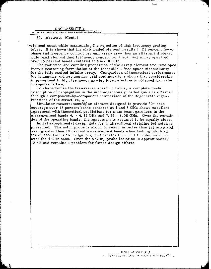
20~ ABSTRACT (Continue on reverse aide It necessary end identify by block iiurnber)
The design and analysis of a unique dual frequency array element andthree probe element exciter for aperture sharing at two widely separatedfrequency bands is presented. The bifurcated twin dielectric slab loadedrectangular waveguide element simultaneously supports a single low fre-quency band phase center and four independently controllable high frequencmphase centers, resulting in the formation of an independent radiating beanmin each band. The principle element design objective is to minimize the
DD JAN713 1473 EDITION OF I NOV 551IS OBSOLETE -UNCLASSIFIED ___
SECURITY CLASSIFICATION OF THIS PAGE Ribrn fTsra fIrred)
/1/
UNC LASSIFIEDSECURITY CLASSIFICA-ION OF THIS PAGE(When Data Entered)
20. Abstract (Cont.
welement count while maximizing the rejection of high frequency gratinglobes. It is shown that the slab loaded element results in 21 percent fewerphase and frequency control per unit array area than an alternate diplexedwide band element dual frequency concept for a scanning array operatedover 15 percent bands centered at 4 and 8 0Hz.
The radiation and coupling properties of the array element are developedfrom a scattering formulation of the feedguide - free space discontinuityfor the fully excited infinite array. Comparison of theoretical performancefor triangular and rectangular grid configurations shows that considerableimprovement in high frequency grating lobe rejection is obtained from thetriangular lattice.
To characterize the transverse aperture fields, a complete modaldescription of propagation in the inhomogeneously loaded guide is obtainedthrough a component-by-component comparison of the degenerate eigen-functions of the structure.
Simulator measurement 'rf an element designed to provide 600 scancoverage over 15 percent baAds centered at 4 and 8 GHz shows excellentagreement with theoretical predictions for main bea m gain loss in themeasurement bands 4. - 4. 32 GHz and 7. 36 - 8.08 GHz. Over the remain-der of the operating bands, the agreement is assumed to be equally close.
Initial experimental design data for unidirectional stripline fed notch ispresented. The notch probe is shown to result in better than 2:1 mismatchover greater than 10 percent measurement bands when looking into loadterminated twin slab feedguides, and greater than 50 dB probe isolationover the 4 GHz band. Over the 8 GHz, probe isolation is approximately12 dB and remains a problem for future design efforts.
UN CLASSIFIED,F IUIT Y .. A . . r 1, . . .. . .. A. '.. , ... , ........

EVALIUATI ON
1. This report is the Final Report of Contract F19628-75-C-0197.
It covers the analytical and experimental investigations of the
bifurcated twin dielectric slab loaded rectangular waveguide dual
frequency array element. The report describes analytical studies
of the infinite array and documents operation at two 15% frequency
bands centered at 4GHz and 8GHz. In addition, the report presents the
experimental results and examination of the strip-line fed notch exciter
which is used at bolh equency ranges.
ROBERT J. MAILL
Project Engineer
1111~ k $11ONS tM
,,t~~ISIIFiCA t.. .-.... ....
.................... D
, v............ .... .. ....... ......... .......... D' D C ' l -
.. ,,, _,. , ci- ":JUL 7 ;"
ii

ACKNOWLEDGEMENT
The authors would like to extend their appreciation to Ms. Joni
Bursey for her considerable help in the preparation of this manuscript.
PA&,UI D I2V
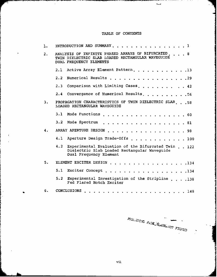
TABLE OF CONTENTS
1. INTRODUCTION AND SUMMARY . ................ .. 1
2. ANALYSIS OF INFINITE PHASED ARRAYS OF BIFURCATED . . 8
TWIN DIELECTRIC SLAB LOADED RECTANGULAR WAVEGUIDEDUAL FREQUENCY ELEMENTS
2.1 Active Array Element Pattern ... . . . .13
2.2 Numerical Results .. ................. .29
2.3 Comparison with Limiting Cases ... .......... .42
2.4 Convergence of Numerical Results . . ........ 56
3. PROPAGATION CHARACTERISTICS OF TWIN DIELECTRIC SLAB. . .58LOADED RECTANGULAR WAVEGUIDE
3.1 Mode Functions . . . . . . . . . . . . . . . . .. 60
3.2 Mode Spectrum ....... .................. 81
4. ARRAY APERTURE DESIGN ...... ................. 98
4.1 Aperture Design Trade-Offs .... ............ 100
4.2 Experimental Evaluation of the Bifurcated Twin 122Dielectric Slab Loaded Rectangular WaveguideDual Frequency Element
5. ELEMENT EXCITER DESIGN ........ ................ 134
5.1 Exciter Concept ....... .................. 134
5.2 Experimental Investigation of the Stripline .. . .138Fed Flared Notch Exciter
6. CONCLUSIONS . ........................ 148
vE OT
Vii!

Table of Contents (Cont.,)
APPENDIX A . . . . . . . . . . . 150
EVALUATION OF THE E FOR RECTANGULAR LATTICEpgrjnm
APPENDIX . . . . . . . . . . . .159
DERIVATION OF DIFFERENTIAL EQUATION RELATING e AND h
APPENDIX C. . . .. . . . . . . .164
ORTHONORMALIZATION OF FEEDGUIDE MODE FUNCTIONS
APPENDIX D. . . . . . . . . . . .172
PROGRAM LISTINGS . . . . . . . . . .173
REFERENCES ................ 231
viii
= !_7 7_
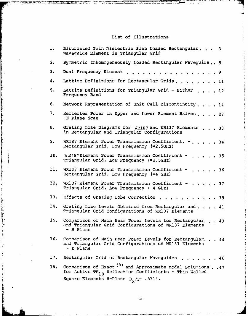
List of Illustrations
1. Bifurcated Twin Dielectric Slab Loaded Rectangular. . . 3
Waveguide Element in Triangular Grid
2. Symmetric Inhomogeneously Loaded Rectangular Waveguide.. 5
3. Dual Frequency Element . . . . . . .. . . . .9
4. Lattice Definitions for Rectangular Grids . . . . . . . . 11
5. Lattice Definitions for Triangular Grid - Either . . . . 12Frequency Band
S6. Network Representation of Unit Cell Discontinuity . . .. 14
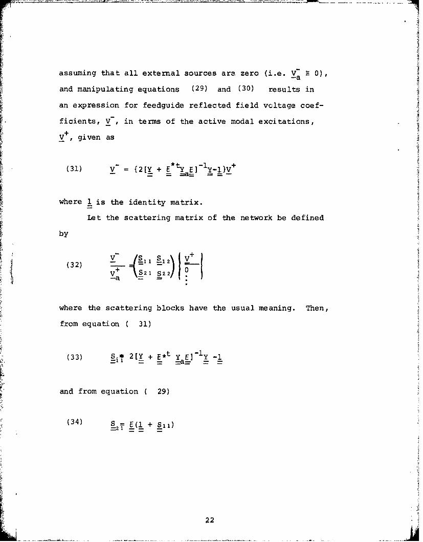
7. Reflected Power in Upper and Lower Element Halves . . . . 27-E Plane Scan
8. Grating Lobe Diagrams for WR187 and WR137 Elements . . . 33in Rectangular and Triangular Configurations
9. WR187 Element Power Transmission Coefficient. - . . . . 34Rectangular Grid, Low Frequency (=2.SGHz)
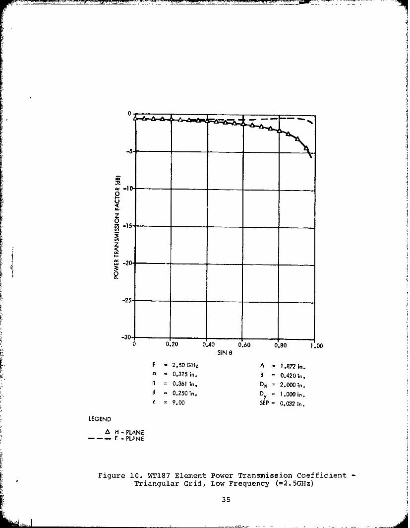
10. WR87Element Power Transmission Coefficient - . . . . . 35'Triangular Grid, Low Frequency (=2.5GHz)
11. WR137 Element Power Transmission Coefficient - ...... 36Rectangular Grid, Low Frequency (=4 GHz)
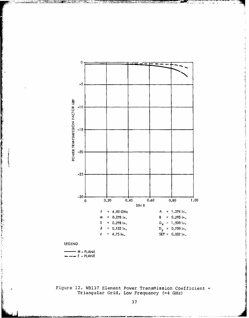
12. WR137 Element Power Transmission Coefficient - ...... 37Triangular Grid, Low Frequency (-4 GHz)
13. Effects of Grating Lobe Correction . . . . . . . . . . . 39
14. Grating Lobe Levels Obtained from Rectangular and . . . . 41Triangular Grid Configurations of WR137 Elerients
15. Comparison of Main Beam Power Levels for Rectangular. . . 43and Triangular Grid Configurations of WR137 Elements
- H Plane
16. Comparison of Main Beam Power Levels for Rectangular.. . 44and Triangular Grid Configurations of WR137 Elements
- E Plane
17. Rectangular Grid of Rectangular Waveguides . . . . . . . 46
18. Comparison of Exact (8) and Approximate Modal Solutions .47for Active TEl0 Reflection Coefficients - Thin Walled
Square Elements H-Plane D/A= .5714.
ix
List of Illustrations (Continued)
19. Comparison of Exact (8) and Approximate Modal Solutions. . 48for Active TEl0 Reflection Coefficient - Thin WalledSquare Elements H-Plane Dx/= .6205.
x20. Comparison of Exact(8) and Approximate Modal Solutions . . 49
for Active TE Reflection Coefficient - Thin Walled10
Square Elements H-Plane DxA= .6724.
21. Comparison of Modal Solutions for Active TEl0 . . . . . 51
Re Jection Coefficient - Thick Walled Square Elements -
H-Plane D /XA= .5714, t = .D x
22. Comparison of Modal Solutions for Active TEl0 . . . . . 52
Reflection Coefficient -Thick Walled Square Elements-H-Plane Dx/X = .6205, t = .lDx
23. Comparison of Modal Solutions for Active TE 0 . . . . . 53
Reflection Coefficient - Thick Walled Square Elements -
H-Plane Dx/X = .6724, t = .IDX
24. Comparison of Modal Solutions for H-Plane Element. . 54Pattern When Aperture Field is Approximated by TE Mode
1025. Comparison of Modal Solutions for H-Plane Element . . . . 55
Pattern When Aperture Field is Approximated by TEl0 + TEModes.
26. Dual Band Element .. ............ . . . . . . . . . . .59
27. Equivalent Transmission Line Representation of Wave . . .. 71Propagation in x.
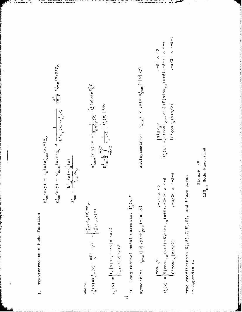
28. LSMn Mode Functions ....... . . . . . . . . . . . .. 72
29. LSEnm Mode Functions . . . . . . . . . . . ....... 73
30. ey1 0 (x,y) Distribution for WR187 Bifurcated Guide With. 75
.250" Thick Er = 9 Loading. 2.5 GHzKr
31. eyl 0 (x,y) Distribution for WR187 Bifurcated Guide With.. 76
.250" Thick er = 9 Loading. 6 GHz
32. ey1 0 (x,y) and ey2 0 (x,y) Distributions for WR187. . . . . 77
Bifurcated Guide With .250" Thick er = 9 Loading. 6 GHz
33. eyl 0 (x,y) and ey20 (x,y) Distributions for WR187 79
Bifurcated Guide With .250" Thick er = 5 Loading. 6 GHz
x

List of Illustrations (continued)
34. Disposition of Roots of D(K,K.) Along Real K. Axis ... 84
35. LSE Dispersion Diagram for Bifurcated WRI87 Guide With 85250" Thick Er = 9 Loading
36. LSE Dispersion Diagram for Bifurcated WR137 Guide With • 89250" Thick e 3 Loading
37. LSE Dispersion Diagram for Bifurcated WR137 Guide With, • • 90.250" Thick Er = 5 Loading
38. LSE Dispersion Diagram for Bifurcated WR137 Guide With . . 91.250" Th..k er 7 Loading
39. LSE Dispersion Diagram for Bifurcated WR137 Guide With . 92.250" Thick er = 9 Loading
40. LSE Dispersion Diagram for Bifurcated WR137 Guide With 93.063" Thick er = 5 Loading
41. LSE Dispersion Diagram for Bifurcated WR137 Guide With 94.125" Thick Er = 5 Loading
42. LSE Dispersion Diagram for Bifurcated WR137 Guide With .95
.188" Thick er = 5 Loading
43. LSE Dispersion Diagram for Bifurcated WR137 Guide With . . 96.375" Thick er = 5 Loading.
44. Equilateral Triangle Lattice Configuration Which . . . . . 101Minimizes Element Count @ 4 GHz.
45. Triangular Grid Configuration for Dual Frequency Operation .108Operation over 16% Bands Centered at 4 GHz and 8 GHz
46. E- and H- Plane Performance of Designed Element,. . . . . . 110K f = 3.68 GHz
47. E- and H- Plane Performance of Designed Element,. . . . . .1f = 4.0 GHz
48. E- and H- Plane Performance of Designed Element,. . . . . . 112f = 4.32 GHz
49. Propagating Beam Power Levels - H-Plane Scan, . . . ... 113f 7.36 GHz
50. Propagating Beam Power Levels - H-Plane Scan, ..... 114f = 8.0 GHz
51. Propagating Beam Power Levels - H-Plane Scan, . ..... 115f = 8.64 GHz
LA

List of Illustrations (continued)
52. Propagating Beam Power Levels - E-Plane Scan, . . . . . . . 116f = 7.36 GHz
53. Propagating Beam Power Levels - E-Plane Scan, . . . . . . 117f = 8.0 GHz
54. Propagating Beam Power Levels - E-Plane Scan, . . . . . . . 118f = 8.64 GHz
55. Waveguide Simulator for Designed Element . . . . . . . .. 119
56. Simulator Imaging of Element Section .. . . . . . . . . . . 123
57. Measured Simulator Port, Impedance 4.0 - 4.32 GHz. . . . . 124Sampled in 80 MHz Increments
58. Comparison of Measured and Predicted Reflections . . . . . 127Coefficient Magnitude at the Simulator Port, 4.0 -
4.32 GHz
59. Port Definitions for 7.32 - 1.08 GHz Simulator . . . . . . 129
60. Measured Simulator Port Impedance 7.32 - 8.64 GHz. . . . . 131Sampled in 160 MHz Increments
61. Comparison of Measured and Predicted Reflection . . . . . 133Coefficient Magnitude at the Simulator Port, 7.32 -
8.00 GHz
62. Stripline Fed Notch Exciter for Twin Dielectric Slab . . . 135Loaded Rectangular Waveguide Dual Frequency ArrayElement
63. Basic Notch Exciter. . . . . . . . . . . . . . . . . . . 137
64. Baseline Notch Exciter Design. . . . . . . . . . . . . . .140
65. Measured VSWR for the P.5 Exciter, 4 to 6 GHz . . . . . . . 142
66. Measured VSWR for the P1 Exciter, 7.5 to 8.5 GHz . . . . . 144
67. Measured Probe Isolation, 3.5 to 8.5 GHz . . . . . . . . . 146
xii
List of Tables
1 Dimensions (in.) of WR187 and WR137 Elements .......... . .31
2 Dispersion Relations for Inhomogeneously Loaded ........ .82Rectangular Waveguide
3 Prescribed Array Performance ............... 99
4 Performance of Dual Frequency Element ..... .......... .105
5 jpen Circuit Stub Lengths for Experimental Exciters . . .141
:1

1. IATRODUCTIOiA AND SUMMARY
This report summarizes the analvtical and experimental
investigations of the infinite array radiation and coupling
properties of bifurcated twin dielectric slab loaded rec-(1)tangular waveguide dual frequency array elements con-
ducted under Contract F19628-75-C-0197. Specifically,
the report presents:
.The complete analysis of the element in infinitearray configurations.
Theoretically determined element/grid designtrade-off conclusions, leading to a proposedconfiguration for operation over 15% bandscentered at 4GHZ and 8GHZ.
.Experimental verification of the analyticalresults and the examination of a unique strip-line fed notch antenna mode exciter.
.The computational details and computer programsdeveloped during the study.
-4R

The bifurcated twin dielectric slab loaded rec-
tangular waveguide dual frequency array element shown
in Figure 1 is a unique concept for providing simul-
taneous aperture usage at two widely separate frequency
bands. At low frequency both upper and lower halves
of the waveguide are excited in-phase with equiamplitude
signals. For moderate slab loading (assuming relatively
thin slabs) this array will behave similarly to a rec-
tangular waveguide array excited in the TEl0 mode with
scan behavior associated with these elements in the
basic lattice (either rectangular or triangular). At
the high frequency the first odd and even half-waveguide
modes can be independently specified such that four
phase centers are defined; within a single low frequency
cell the fields are confined predominately to the slab
regions.
For practical array designs, the low and high
frequency lattice cells are identifical, and the prin-
cipal element/grid design trade-off is to minimize the
number of phase centers (or phase shifters) while main-
taining main beam purity and gain over a specified scan
volume, particularly in the high frequency band. Con-
sequently the lattice is selected such that element
spacing is not optimum for either band, but presents
the best compromise of element count versus grating
2

PHASE SHIFTWALL
Figure 1. Bifurcated Twin Dielectric Slab Loaded Rectangular~Waveguide Element in Triangular Grid
K V 3
lobe free scan volume in the high frequency band. At
scan conditions for which high frequency grating lobes
are entering or present, the multimode aperture excita-
tion is adjusted (slightly) to cancel the grating lobe.
These considerations are treated fully in Section 2
which gives details of the analysis of array performance,
and section 4 which summarizes design tradeoffs and ex-
perimental results.
The application of the twin dielectric slab
loaded element to dual frequency aperture sharing follows
from the unique propagation properties of the inhomo-
generously loaded structure. The symmetric loaded guide,
shown in Figure 2, is inherently wideband. At sufficiently
low frequency, a single guide mode (the LSE 1 0 mode) propo-
gates and has an electric field distribution somewhat
broader than the homogeneously loaded guide TE1 0 dis-
tribution. As frequency is increased, the LSE 2 0 mode
enters, having electric field distribution similar to
the TE20 distribution of the homogeneously loaded guide.
Concurrently, the LSE10 distribution begins to develop
a minimum along the guide mid-plane. At sufficiently
high frequency, the distributions become essentially
identical, except for symmetry about the mid-plane, and
the ratio of longitudinal wavenumbers approaches unity.

i "" I
-I--O
H - A _
~ 5

By appropriate selection of guide, slab permittivity,
and operating points such that only the two modes propa-
gate, the guide will simultaneously support a single
propagating low frequency mode with phase center at the
midplane, and a conglomerate high frequency distribution
with two independent phase centers at (roughly) the slab
centers. The analysis of propagation in the inhomogenously
loaded guide is given in Section 3.
In general, he dispersioii in the inhomogeneously
loaded guide is not linear in frequency. Consequently, the
use of a bidirectional exciter requires load terminations
at the back of the guide to ensure the proper aperture
field phase at both frequencies, and results in a 3 dB
power loss. This difficulty is alleviated by a unique uni-
directional exciter consisting of three stripline fed flared
(2,3,4)notch antennas inserted into the back of the feed-
guide in suc h a manner as to provide a minimum of 25 dB
frequency band isolation. Preliminary experimental investi-
gation of this exciter design concept was begun during this
study, and is discussed in Section 5.
Four appendices are included. Appendices A, B, and C
give the details of the analysis. Exp±icit expansions of
modal coupling coefficient integrals are given in Appendix A.
In Appendix B, the derivation of the differential equations
6
relating feedguide modal fields is given. And in Appendix
C, explicit expressions for feedguide mode orthonormaliza-
tion in'cegrals are given. The remaining appendix gives
complete listings of all programs required to reproduce the
numerical results given in this report.
A time dependence e is assumed throughout.
A
IZ
L 7

2,0 ANALYSIS OF INFINITE PHASED ARRAYS
OF BIFURCATED TWIN DIELECTRIC SLAB LOADED RECTANGULAR
WAVEGUIDE DUAL FREQUENCY ELEMENTS
In this section, the formal solution for the radiation
properties of the element in infinite array configuration
is presented. The unique property of the bifurcated twin
dielectric slab loaded rectangular waveguide dual freq-
uency array element is that it possesses five phase centers:
one, associated with the low frequency band operation; and
the remaining four, with a high frequency band. By appropri-
ate exciter design, the element can simultaneously operate
over both bands.
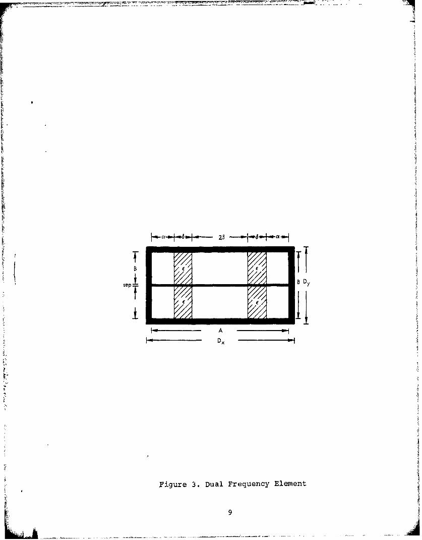
The basic element is shown in Figure 3. Arrays are
formed by stacking these elements in rectangular or tri-
angular grid configuration. The element consists of a
rectangular waveguide bifurcated in the E-plane by a
septum of thickness 6. Outer dimensions are Dx and D ana
inner dimensions, A and B', where D and A are associatedx
with the x coordinate. Four half height lossless dielectric
slabs of thickness 6 and relative dielectric constant rr
are located at distance a + 6/2 (on center) from the narrow
8
714
sep . _. ( B D
i -o-
LD
i -. - t
- Figure 3. Dual Frequency Element
K3

walls. At low frequency, a phase center is maintained at
the element center (i.e., over the septum) by exciting the
LSEI0 mode equally in the two half guides. At high freq-
uency, four independent phase centers, at roughly the four
slab centers, are formed by appropriately exciting the
LSEI and LSE modes in each half guide.L 10 20
When the elements are arrayed in a rectangular grid
the element lattice vectors, s, and s 2 are as shown in
Figure 4a, provided the septum thickness, 5 , is not equal
tOo -Bgk. When . = -B'*the low frequency lattice isy y )
as shown in Figure 4a, and the high frequency lattice is
as shown in Figure 4b, When arrayed in a triangular
grid, the lattice vectors are defined as in Figure 5,
regardless of operating frequency or septum thickness.
In section 2.1, the formal solution for active array
element pattern is given. The method of solution is
similar to that developed by Lewis, et al( 5) for the
analysis of a parallel plate array with protruding dielec-
tric. In the present work, the formalism is extended
to two dimensional array cells, and the unique dual freq-
uency urnit cell geometry is accounted for. In section 2.2J
numerical results are presented and particular attention
is given to the disposition of high frequency band grating
lobes. Discussion of grating lobe suppression is deferred
10

(a) Septum ThIckneSs,S= Dy-B, High and Low Frequencie
(biseptum Thickness 09=Dy-B, High Frequency
Figure 4. Lattice Definitions for Rectangular Grids
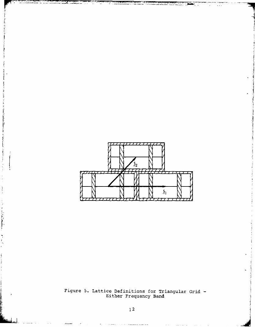
Figure 5. Lattice Definitions for Triangular Grid -
Either Frequency Band
12

_______~7 =-tiZ~ - =77 M.. 2 ---
to section 4.1. In section 2.3, numerical results are
checked against published data for several limiting geom-
etries. 3
2.1 Active Array Element Pattern
The active array element pattern is determined from
a unit cell formulation of scattering at the feedguide
free space interface. The interface is taken as coincident
with the z = 0 plane, with the array elements occupying
the z < 0 half space. The scattering matrix, S, which
relates feedguide modal voltages to the modal voltages of
the space harmonics, in the manner indicated by the network
in Figure 6, is obtained by matching the transverse-to-z
fields in the cell across the interface. The field matching
is accomplished via Galerkin's method, from which the scat-
tering formalism follows directly. Active array trans-
mission coefficient is then obtained from the network.
In the following discussion, the assumed cell configuration
is that shown in Figure 4a. The extension of these
results to either of the other two cases is straight
forward.
For the configuration of Figure 4a, the unit cell
perimeter may be taken as coincident with the element
outside perimeter. Thus, the unit cell overlays two
13

n FEEDGUIDE m CELLMODAL TRANSMISSION HARMONICMODAL TTRANSMISSIONLINESLINES
V" V"
Figure 6. Network Representation of Unit Cell Discontinuity
14

independent aperture regions and the modal representation
of total transverse-to-z electric and magnetic fields at
z =0- is given as
(1) Et(s) = ((S)+O(-Y) .Vj (S)1 j
(2) H_(s) = U(y)I>ih>(s)+U(-y)zI< h (s)i j
where
(3)
(I 0,>0
The subscripts > and < are used to distinguish the two
aperture regions. V and I are modal voltage and
current coefficients, and are related by
(4) 1 V
where Y is the modal admittance of the i aperture
mode, and the single ordering index i is used to simplify
notation. The mode functions e and h are given in
section 3.1.
iisL! 15

At z = 0+ , the unit cell guide representation of
transverse-to-z fields, over the full cell, is
(5) (S) = Vapq reapqr (S)pqr
(6) Ht(S) = h (s)
(6)pq !i apqr apqr-
where (6)
(7) -api)= -KXo-apqr (s)
()e (S) e [(2-fl)k + (r-1(8) eapqr - /' tpq -tpq (-) ktpqXo]
(9)r =1 for E modes with respect to z
F r2, for H modes with respect to z
(10) ktq=k x +k =ksino(cosoLo+sin 0 yo)
(10) -tpq xpq-oypqo o
+pt1+qt2
11) k xpq ksinO coso +pt + qt2
16
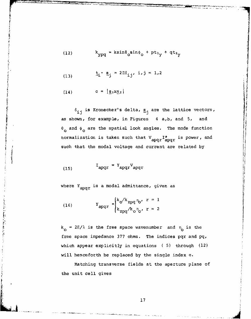
(1)kypq i sin O + pty qtay
II ypq 0 0 y y
s~i . 2 116 i* i1?] 1,2
(14) C = SlXS21
6.. is Kronecker's delta, s. are the lattice vectors,
as shown, for example, in Figures 4 a,b, and 5, and
8a and oare the spatial look angles. The mode function
normalization is taken such that V I* is power andapqr apqr
such that the modal voltage and current are related byAl
(15) apqr YapqrVapqr
where Y is a modal admittance, given as(6 apqr
a k/ zpq =2, r 2
k= 211/A is the free space wavenumber and no is the
free space impedance 377 ohms. The indices pqr and pq,
which appear explicitly in equations ( 5) through (12)
will henceforth be replaced by the single index o.
Matching transverse fields at the aperture plane of
the unit cell gives
LA 17

U (Y) EV .e:? (s) +U (-) V je (s ,
(17) £Vaeao(S) =10, elsewhere in the aperture
and
(18) ZI ha(s)=U(y) .I>1(s)+U(-y)7I<js)
in the aperture
Approximate solutions for the parameters of the network in
Figure 6 are obtained when the modal series are truncated.
As a result of the truncation, the continuity equations
(i.e., equations (17) and (18) can no longer be exactly
satisfied, and vector error terms A, and A2 must be inserted
to restore the equality. These error terms are given as
a (s)-U(y) V .e>i(s) +U(-y) Vj e (s),Vaaa - i- -
(19) in the apertures
a ea (s), elsewhere
and
M J
(20) A2= Iaohao (s) -U Z<(y) ji . (s)
in the apertures.
18

It is now required that the projections of A, and A2 onto
the appropriate modal spaces be zero.
The domain of definition of Et(s) is over the entire
unit cell, and the domain of E (s) may be artificially
extended over the metalic portions of the cell. Thus, the
domain of A, is the unit cell, and the modal subset span-
ning the space are the ha(s). Requiring orthogonality of
A, to the h(s) and performing the inner products over the
cell results, after manipulation, in
(21) V =E>V + E<V
where is a matrix of coupling coefficients, the elements
of which are given as
(22*) <E = dAe(s).(h*(s)xz O)
1/2 cell
The elements of the column vectors V> are the feedguide
modal voltages.
The domain of definition of A2 is over the aperture
only. Therefore, the appropriate basis spanning this space
is formed by the concatination of the trunicated modal
iComplete expressions for E are given in Appendix A
19
sets which individually span only one or the other f the
aperture region spaces. Such a basis may be represented
by the partitioned vector B(s), given as>U(y)e (s)
(23) (s)= _ -- < -;
U(-y)e (s)
Requiring orthogonality of A2 on the space spanned by
B(s) results in
(24) I=....I, - a
I< j
where X< are submatrices of coupling coefficients, the
elements of which are given as
(25) I dA[h (s)xzo]"ei*(s)f0 -aoa- -0o 1
1/2 aperture >e >
Since the e.(s) and ej(s) may be artificially extended to
individually span the appropriate entire half cell,
20

(26) =<*r ,0 0,n
It is convenient, then, to define the partitioned vector
V such thatv V:(27)
and the partitioned matrix E as
(28) E = ( >IE<)
Then, the voltage and current equations, (3-21) and (3-24),
respectively, take the form
(29) V = E V-a
(30) I =E~tl
where the asterisk denotes conjugation and the t denotes the
transpose operation.
The vectors V, V, I, and I in equations (29) and- - -a
(30) are total modal voltages and currents. Using the
conventions established for the network in Figure 6,
21
assuming that all external sources are zero (i.e. Va 0),
and manipulating equations (29) and (30) results in
an expression for feedguide reflected field voltage coef-
ficients, V, in terms of the active modal excitations,
+V ,given as
(31) V- = {2[Y + E* El-Y-1}V+
where 1 is the identity matrix.
Let the scattering matrix of the network be defined
by
V ji; ~~(32) V- - S
-a S21
where the scattering blocks have the usual meaning. Then,
from equation ( 31)
(33) S- 2[Y + ,t y ElY -1-- - - -a-
and from equation ( 29)
(34) S = E(l + Si,)=2 ! __ __
L: 22

with V- - 0.-a
In more standard array configurations, the feedguide
and aperture are designed for single feedguide mode propa-
gation in a single frequency band. In these configurations,
the active array reflection coefficient is simply the one
element of S1 1 corresponding to reflections in the domin-
ant mode. Defining that matrix element as T(eo o), norm-
alized active array element gain pattern is
(35) ge(e0) = (1- l(e,4o) )coseo
provided no grating lobes have entered real space. Follow-
ing the entrance of the first grating lobe, it is necessary
to track the propagating beams individually, and the
relative power in the a beam due to the single excited
mode (i=l) is
(36) P (0 ,f ) = IT (60,0)I Yaa/YI
where T (0,f) is the (a,i)th element of the partitioned
block S2 ,, and ea and a are the actual location angles of
the ath beam.
23

Active array element pattern is defined in a different
manner for the array of bifurcated twin dielectric slab loaded
rectangular waveguides. In this instance, the aperture is
always considered to be multimode. In the low frequency
thrange, the LSEI0 mode (ordered as the i h ) is excited
equally, in amplitude and phase, in both regions of the aper-
ture. Consequently, for an I-mode feedguide aperture field
approximation in both upper and lower regions, the power in
the main beam, a--m, is given, for principle plane scan*,
as
(37) P (6O,cO) = 1/21 rli( 0 ,wo) + S'i'(O,4 Y /Y.m am
where s2 (e,p) is the (m,i)th element of S21, and the
thi feedguide mode is the propagating LSEI0 mode. By the
definitions in equations (27), (32), and (34),
sm21 (80, O) is the voltage transmission coefficient for coupling
from the ith mode in the upper aperture region to the mth
Equation (3-37) is strictly valid only for e0O0 andin the principle planes (0=0,1, or O=H/2, 311/2). For allother scan planes (and at broadside), the total power in themain beam is the sum of the powers in the dominant (p=q=o)Eand H modes.
L 24

beam in free space; and S21 is the voltage transmission
from the ith mode of the lower aperture region to the mth
beam*.
Active array reflection coefficient is also obtained
via superposition. For the multimode aperture configuration,
it is necessary to independently track all propagating waves
in the feedguide. Hence, for low frequency excitation,
the total reflected power in the LSEI0 mode of the upper
aperture region is given, for any scan angle, as
(38) R>(0o,0o) = 1/21Si'i(6o, 40 ) + Sii+I(eo,po)2
For the lower aperture region, the reflected power is
i+I'i _i+I,i+I(0,)
(39) R< (0o,o) 1/21SIu (60,*0) + S11 (Oo,po)1
where Srit(00,,0) is the voltage scattering coefficient
th thfrom the r aperture region mode to the t aperture region mode.
It is evident from these two equations that the reflected
powers in the two regions are not necessarily equal.
Indeed, it is found that for low frequency excitation,V>
R (eo,oo) equals R (00,0o) only in the H plane of scan.
*It is assumed that the mode ordering in the two apertureregions is the same. This assumption will carry throughthe remainder of the report.
,25

As an example, reflected power is shown versus E plane
scan angle in Figure 7. The element is a WR187 guide with
.250" thick slabs of cr=9 dielectric located .450", on center,
from either narrow wall and with a .032" septum.
The operating frequency is 2.5 GHz. There is considerable
difference in reflected power between upper and lower
regions throughout the scan range .17 <sine<.95. Consequently,
low frequency excitation of the upper and lower regions of
the element from a common post phase shifter feed point, as
is desireable for several low frequency feed concepts, will
produce an imbalance at the outputs of the power divider net-
work. Since the impact of this effect on feed and exciter
design is beyond the scope of this study, it will be given
no further consideration in this report.
At the high frequency band, the element is excited
such that four independently controllable phase centers are
distributed in the aperture. To maintain this phase center
distribution, four propagating modes, two in each region,
are excited. The modes are LSEI0 and LSE 20 For sufficiently
high frequency and dielectric constants, these two modes have
nearly equal dispersion. In addition, to a crude approxi-
mation, the modal field distributions, e" and e" differ
26
0*
-5-
S-10-
9L
LU
4 -15-
- PER APERTURE REGION
LOWER APERTURE REGION/-20--
-25-0 0.2 0.4 0.6 0.8 1.0
$in e
F'igure 7. Reflected Power in Upper and Lower Element Halves-B Plane Scan
27
only in symmetry and behave like jsin(2i1x/A) land sin(2J1x/A)
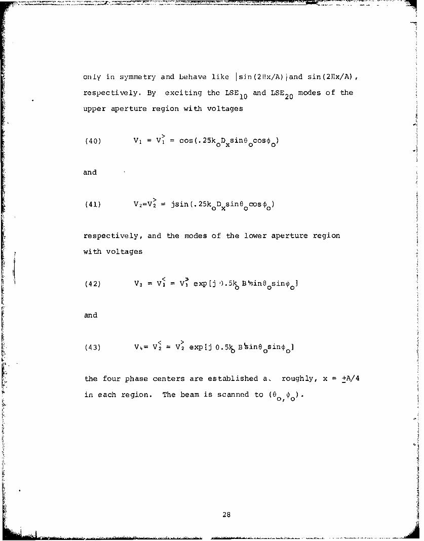
respectively. By exciting the LSE and LSE modes of the10 20
upper aperture region with voltages
(40) V, V1 cos(.25k 0 D si 0 cos 0 )
and
(41) V2=V2 jsin(.25k D snOcos40 )
respectively, and the modes of the lower aperture region
with voltages
L(42) V3 =V1 V1 exp[j ').5k B'.t-inO sinp0 0 0
and
(43) V4= V2 V2 expl 0. 5]k, Bine sin p0
the four phase centers are established a, roughly, x =+A/4
in each region. The beam is scanned to (001 V)
0, 0
28

?I
As for low frequency, the normalized power in the
high frequency propagating beams is determined via super-
position (i.e., using equation (29)). The total power
delivered is
(44)> 2 > 2P-- 2[Y11V11 + Y21V21 - Y+Y 2]
The power in the ath beam is therefore, given as
4 i 2(45)* P0 (O ,p O) = IZ S21 ( 0 ,4o)Vi Y/Pi=l a
where the ordering of the elements of V has been altered
to simplify the equation. Taking the same liberty with
mode ordering, the power reflected in the jth mode
(j = 1,2,3,4) is given as
4(46) Rj(eo = I S i(e ) y/P(4i61 0 01 0 j
2.2 Numerical Results
In this section, numerical results are presented
for several element and grid geometries to illustrate the
principle performance ciaracterioCioo u." t U bifurcateu
*See footnote to equation (37)
. 2-0

twin dielectric slab loaded rectangular waveguide dual freq-
uency array element. Element/grid design is discussed more
fully in section 4.
For purpose of discussion, it is convenient to present
performance data in a somewhat unusual format. Rather than
present realized gain pattern, (i.e., normalized directive
gain) power transmission coefficient is given for each
radiating beam. The advantage gained by this form of pres-
entation is that it allows a direct comparison of the power
in the radiated beams. If P (0 4 is the power associated
with the th beam when the main beam is scanned to (00, O),
then the directive gain of this beam is proportional to
P, (0, d coseo. Consequently, for a given scan angle, com-
parison of beam directive gains includes the comparison of
projected aperture at the various beam locations.
Data are presented for rectangular and triangular grid
configurations. Two elements are discussed: a WR187 guide
with .250", cr= 9 slab loading; and a WR137 guide with .125",
r= 4.75 slab loading. The former is operated at 2.5 GHz
(kA/2=1.246) and 6.0 GHz (kA/2=2.990). The later is operated
at 4 GHz (kA/2=1.463) ani 8 GHz (kA/2=2.926). The dimen-
sions of the elements are given in Table 1. In the
following, the elements will be distinguished by the WR
number of the rectangular guides.
L 30

WR187 WR137=9= 4.75
r r
D 2.000 1.500
D 1.000 .750 or .960
A 1.872 1.374
B' .872 .622 or .832
6 .032 .032
B .420 .295 or .400
.325 .281
.361 .281
6 .250 .125
Table 1
Dimensions (in.) of WR187 and WR137 Elements
L 31

?I
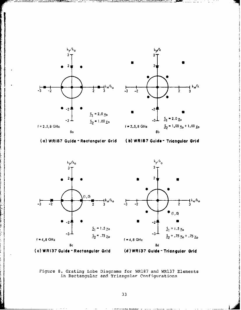
The grating lobe diagrams for the four grids are shown
in Figures 8a,b,cd. Each diagram shows the near in
grating lobe locations for the two operating points. Low
frequency grating lobes are indicated by solid boxes,
and high frequency lobes, by solid dots. What is immediately
obvious from the figures is that the triangular grid provides
a grating lobe free scan region for all directions in the
plane at high frequency. One consequence of this is improved
high frequency broadside match, as is shown below.
Figures 9 through 12 show power transmission
coefficientin the principle planes at low frequency for
each of the four grids. In the scan range sine 0 <.95, no
grating lobes enter, as can be seen from the grating lobe
diagrams in Figure 8. In general, the performance of the
four configurations is the same. There is some improvement
in scan coverage of the WR137 element over the WR187 element,
but the difference is not large enough to show up on the
scale of the figures. In the E-plane (sin4= 1.0), the
fall off is nearly cos /2, out to 600 - the WR187 element
shows slightly greater scan loss. In the H-plane, the scan
loss exceeds cos /2e by approximately .5 db at 8=60 °. As
might be expected, the performance of the rectangular and
triangular grid configurations, as measured by power trans-
32
ky/k0 y/3 3
kw/kO ky/k-3 -2 2 3 -3 -2 2 3
021 0 -2
-3 -31 2 S
f 2.5,8 GHz f 2.5,8 GHz8a 8b
(a) WR187 Guide - Rectangular Grid (b) WRIS7 Guide- Triangular Grid
ky/k0 k /k0
3- 3-
2* 0 1
(1,0)
-3 -22 3-3 -2 3
*-2 -J
1.5 X0 S 1 I.5 x
f 4,8 GHz f2.7 X -i4,8 GHz
8c 8d
(c) WRI37 Guide -Rectangular Grid (d)WR137 Guide -Triangular Grid
Figure 8. Grating Lobe Diagrams for WRl87 and WRl37 Elementsin Rectangular and Trianguilar Configurations
33

-5\
,_ -10-
0)
O
0in -15-I-
0 0.20 0.40 0.60 0.80 .00
SIN 8o
F -2.50 GHz A = 1 .872 in.= 0.325in. B = 0.420 in.
B1 = 0.361 in. Dx = 2.000 in.= 0.250 in. Dy = 1.000 1n.
8 9.00 SEP = 0.032 in.
LEGENDA H - PLANE
E - PLANE
Figure 9. WR187 Element Power TrAnsmission Coefficient -
Rectangular Grid, Low Frequency (=2.5GHz)
: 34
L - ,4
'1
-5-
Zv
-10,
z0
z
Un -205
-25-
-30-0 0.20 0.40 0.60 0.80 1.00
SIN 0
F = 2.50OGHz A = 1.87)2 in.c' = 0.325 in. B = 0.420in.
B = 0.361 in, Dx -'= 2 .000in.
= 0.250in. D = 1 .000in.
= 9.00 SEP = 0.032 in.
LEGEND
SH - PLANE
E - PLANE
Figure 10. WT187 Element Power Transmission Coefficient -Triangular Grid, Low Frequency (=2.5GHz)
35
EA

SAl --.. <
-5
0 -10
z0
I-t
z
Lu -20-
0
-25
-300 0.20 0.40 0.60 0.80 1.00
SIN 0
F = 4.00GHz A = 1.374 in.
a = 0.278 in. B = 0.295 in.
1 = 0.278 in. Dx = 1.500 in.4 = 0.132 in. 0y = 0.750 in.
= 4.75 in. SEP 0.032 in.
LEGEND
- H - PLANE
E - PLANE
Figure 11. WR137 Element Power Transmission Coefficient -
Rectangular Grid, Low Frequency (=4 GHz)
36
-5.
' -100
V)
z0
-25--20
-25 __ __ ___ __ _ __ __ _
0 0.20 0.40 0.60 0.80 1.00
SIN 0
F = 4.00 GHz A = 1 .374 in.
a = 0.278 in. B = 0.295 in.
3 = 0.278 in. Dx = 1.500 in.6 = 0.132 in. Dy = 0.750in.
- 4.75 on. SEP = 0.032 in.
LEGEND
H - PLANE
--- E - PLANE
Figure 12. WR137 Element Power Transhission Coefficient -
Triangular Grid, Low Frequency (=4 GHz)
37
mission coefficient, is not distinguishable, one grid from
the other.
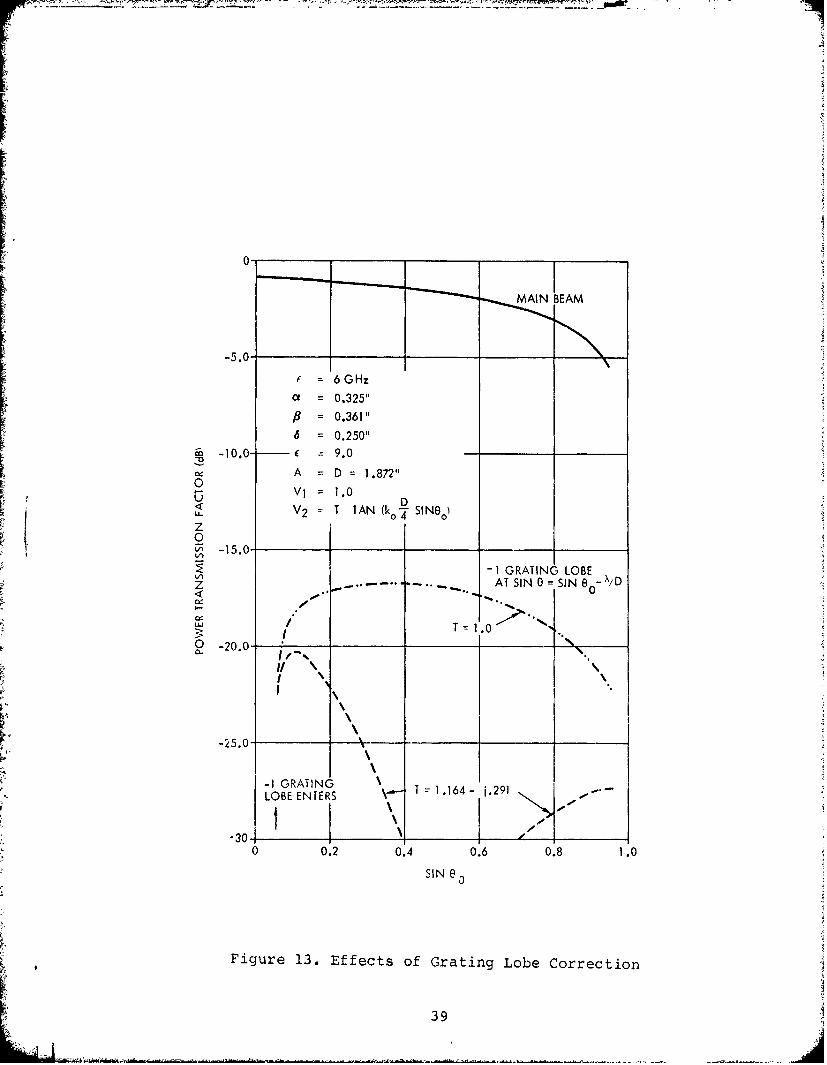
In Figures 8a and 8c, the high frequency grating
lobes of the rectangular grid configurations are shown re-
siding in real space for the no scan condition. In this
situation, a broadside power loss occurs, and a high farout
sidelobe condition is created. To a certain extent, the
power delivered to these lobes can be reduced by introducing
a complex, multiplicative correction for the voltage excita-
tion coefficients, V2 and V4, given by equations (41)
and (43) !7) Ideally, this correction is independent of
scan and frequency (for small bandwidths). Typical
gratin9 lobe levels, with and without the correction, are
L shown in Figure 13 for a thin walled element in a rec-
tangular grid. Without correction, grating lobe levels reach
-16.7 db. With the multiplier 1.164 - j.291*, the maximum
grating lobe level is -20.4 db, and beyond sinSo=.3, the
level is below -25 db. Differences in the main beam due to
the two excitations are too small to be represented in the
figure.
*The case shown here is supplied by R. Mailloux, the multi-plier 1.164 - j.291 was also found suitable for theWR187 element in a rectangular grid.
38
I77
6 = 0.250"
- -10.0- - c - 9.0
0
T- GRATING LOBE
00
0-10.0-
T 0
-20.0
-25.0
K-1 GRATINGLOBE ENTERS T 1 1.164 - .291-
-300 0.2 0.4 0.6 0.8 1.0
SINe 3
Figure 13. Effects of Grating Lobe Correction
39

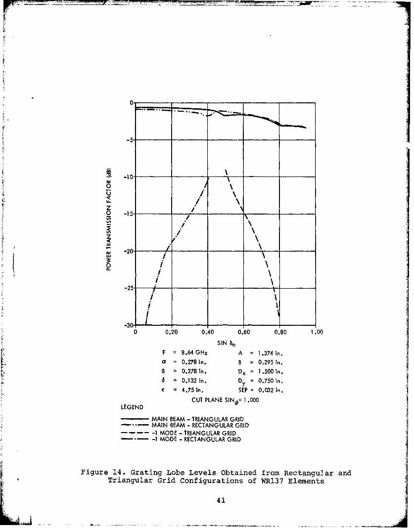
I
By configuring the WRl87 and WR137 elements in triangular
lattice, the difficulties encountered due to the location
of the high frequency grating lobes are largely eliminated.
Figures 8b and 8d, show the disposition of high freq-uency grating lobes for triangular grid. No grating lobes
enter real space along any cut plane for sin60 <.391.
In the principle cut planes, only the main beam is propa-
qating out to sin0 0=.820, or nearly 600 scan.
For wide angle scan applications, the triangular grid
configuration does not fully eliminate the necessity for
the type of excitation correct.on described above. Consider
Figures 8c and 8d. The (1,0) harmonics of the structures
follow the same track for E plane scan, arid while they are
in real space, one is the image of the other, reflected
about the k /k axis. Hence, for the same voltage correc-Xr 0
tion term, ioughly the same amount of power will be dumped
in the triangular and rectangular grid lobes when the
E plane scan sines, sine and sin@r , respectively aretr
related by
(47) sine = X/D - siner y t
This is illustrated in Figure 14 for the WR137 element
operating at 8.64 GHz. Both E and H mode space harmonics
are shown. It is clear from the high power levels shown in
the figure that grating lobe control is required for either
40
-5
2. -10\
0Li
z
/\
i!o i1
i \
0
0 0.20 0.40 0.60 0.80 1.00
SIN B,F = 8.64 GHz A = 1.374 in.a = 0.278 in. B = 0.295 in.
B = 0.278in. Dx = 1.500in.= 0.1321n. Dy = 0.750in.
r 4.75in. SEP = 0.032 in.
CUT PLANE SIN,= 1 .000LEGEND
MAIN BEAM - TRIANGULAR GRID... MAIN BEAM - RECTANGULAR GRID-- -1 MODE - TRIANGULAR GRID
-1 MODE - RECTANGULAR GRID
IC' Figure 14. Grating Lobe Levels Obtained from Rectangu2ar and
Triangular Grid Configurations of WR137 Elements
41LLA

grid type, even though the cosO beam broadening factor is
less than .4 throughout the scan range.
Because of the high grating lobe levels obtained
for the rectangular grids, there is significant (approximately
.1 db) main beam loss at broadside relative to main beam
levels obtained for the triangular grid. For the WR137
element, the difference is .13 db. A comparison of principle
plane main beam levels for the two grids is shown in Figures
15 and 16 . The operating point is 8 GHz. In the H
plane, Figure 15 , the beams show the .13 db difference at
broadside, and smoothly coalesce. In the E plane, Figure
16 , there are sharp jogs in the curves. For the rectangular
grid, the jog occurs as the grating lobe pair exits from
real space. For the triangular grid, the sudden power loss
at sinOD = .82 is due to the grating lobe pair entering
real space. The matn beam falloff is slightly greater than1/2icos/2 eo for both grids in either plane.
2.3 Comparison with Limiting Cases
To check the analysis, and in particular the details
of the computational procedure, several limiting cases have
been examined. For these cases, the slab dielectric con-
stant is set to r=1 and the LSEI0 mode is independently
42

0
-2.0-
zw
U-U-W -4.0 "0Uz0
tA -6.0z
""- - TRIANGULAR GRIDRECTANGULAR GRID
30: -8.0
-10.00.0 0.2 0.4 0.6 0.8 1.0
sin 0
Figure 15. Comparison of Main Beam Power Levels for Rectangular and
Triangular Grid Configurations of WR137 Elements - H Plane
43

0i
II
' -2.0--
Z
u-
0 -4.0
Z
S -6.0z
TRIANGULAR GRID""- --- RECTANGULAR GRID
-8.0-
-10.0
0.0 0.2 0 .4 0.6 0:8 110
in 0
; • Figure 16. Comparison of Main Beam Power Levels for Rectangular andTriangular Grid Configurations of WR137 Elements E Plane
~44
1%,,pA

excited in the upper and lower aperture regions.
For E =l, the LSE modes degenerate to the TEn modesr no no
of empty rectangular waveguide. Therefore, an appropriate
set of check cases include H plane scanned thin wall rectangular
grid arrays of rectangular elements and special triangular
grid examples which have appeared in the literature. Thick
wall rectangular grid cases can also be used as checks
provided the wall thickness is not too great.
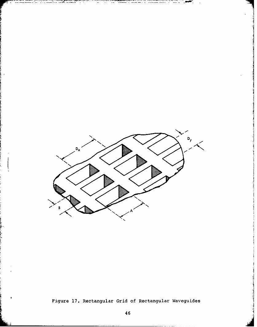
The geometry for the rectangular grid examples is
shown in Figure 17. The aperture dimensions are A and 13,
and the lattice vectors are
(48) S, d xx
and
(49) S = dy-o
For A=dx and B-d , exact solutions for E and i plane
element patterns have been obtained using function theoretic
techniques to construct the reflection coefficient of the
driven TE1 0 mode. (8)Figures 18 through 20 show magnitude and
phase of active reflection coefficient, F, of the TE 1 0 mode of
square waveguide in thin-wall square lattice configuration for If
45
D A
B. A
4
Figure 17. Rectangular Grid of Rectangular Waveguides
46M

0.4- GRATING LOBEsine 0. 7501
0.3-
0.2.
-Wu AND GALINDO(8
0.1 PRESENT ANALYSIS_
0 .1_____ ____
0 0.2 0.4 0.6 0.8 1.0L sin 0
1350
900-
450 _ _ _ _ _ _
0 0.2 0.4 0.6 0.8 1.0sin 0
Figure 18. Comparison of Exact (8) and Approximate Modal Solutionsfor Active TE1 Reflection Coefficients - Thin Walled
Square Elements H-Plane DA/= .5714
47

0.4 !GRATING LOBEsin0 = 0.6116
0.3-
L, o.2
0.1-
Wu AND GALINDO(8)---.- PRESENT ANALYSIS
0 - 10 0.2 0.4 0.6 0.8 1.0
sin 0
1800
1350.
, 900-
450.
00 0.2 0.4 0.6 0.8 1.0
sine
Figure 19. Comparison of Exact(8 ) and Approximate Modal Solutions
for Active TEl0 Reflection Coefficient - Thin Walled
Square Elements H-Plane Dx/= .6205
48
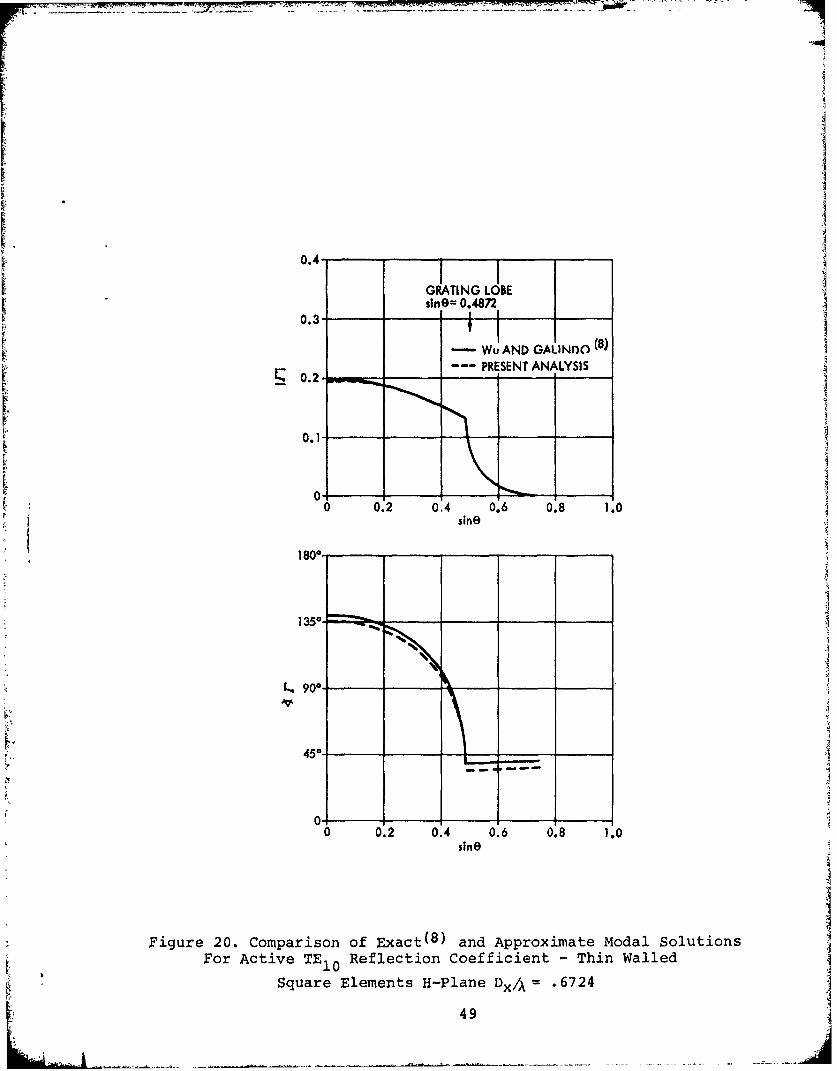
S W ....... ....... -7:77
0.4-
GRATING LOBEsine= 0.4872
0.3
- Wu AND GALINrO (8)
-- PRESENT ANALYSIS
0.1
0
0 0.2 0.4 0.6 0.8 1.0sine
180 °_
135o
C.. 900
45°
00 0.2 0.4 0.6 0.8 1.0
sine
Figure 20. Comparison of Exact (8 ) and Approximate Modal SolutionsFor Active TE1 0 Reflection Coefficient - Thin Walled
Square Elements H-Plane Dx/A = .6724
49 i
plane scan. The solid curves are the exact solution, as(8)
obtained by Wu and Galindo. The dashed curves are obtained
from the current formalism using the first five TEno modes
to approximate the aperture field distrubution. The minor
discrepancies between the results are removable by including
additional higher order modes in the modal computations.
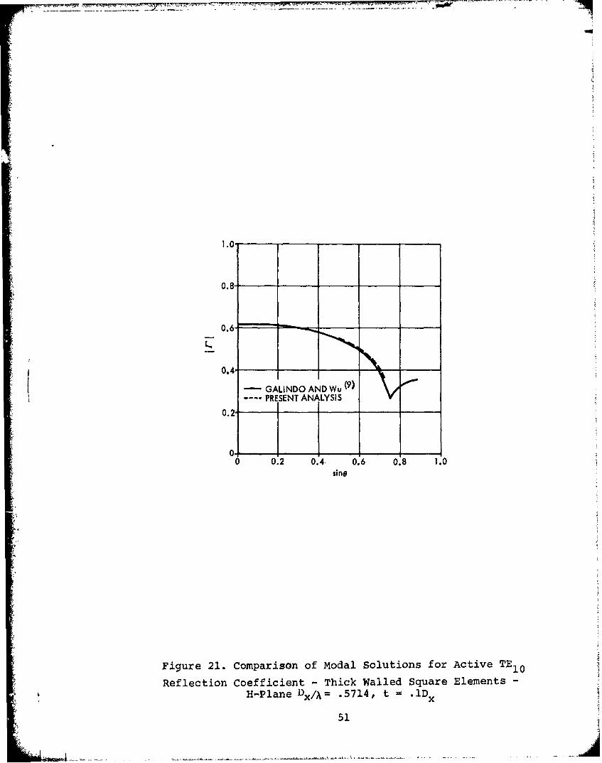
Figures 21 through 23 show magnitude of r as a
function of H plane scan angle when the H plane metalic walls
have finite thickness, t = .ldx . The lattice remains square.xThe solid curves were obtained by Galindo and Wu(9) using
30 feedguide modes to represent the aperture field. The
dashed curves are from the present analysis using the first
nine TEno modes. The agreement is excellent.
Aperture field approximations consisting of the first
few TEno mode functions may be used to compute H plane
element patterns of triangular grid arrays of rectangular
apertures.
Figures 24 and 25 show H plane element pattern,I 2]C (10)
Cl - In ]cosO, as computed by Amitay, Galindo, and Wu
and using the approximate limiting case of the present analysis.
50
1.0-
0.8
0.6
0.2
0- -
0 0.2 0.4. 0.6 0.8 1.0
F'igure 21. Comparison of Modal Solutions for Active TE10Reflection Coefficient - Thick Walled Square Elements -
H'-Plane Dx/A= .5714, t .lDx
51
t
: I -- G LIN. NO u.-

1.0
0.8
-GALINDO AND Wu (9)0.6- - PRESENT ANALYSIS
k
0.4-
0.2, -
0 -0 0.2 0.4 0.6 0.8 1.0
sin 0
Figure 22.,Comparison of Modal Solutions for Active TEl0
Reflection Coefficient - Thick Walled Square Elements -H-Plane Dx/A = .6205, t = .lD
x
L 52

1.0
0.8
0.6,
- -- GALINDO AND Wu (9)---- PRESENT ANALYSIS
0.4
010 0.2 0.4 0.6 0.8 1.0
sin 0
Figure 23. Comparison of Modal Solutions for Active TEl0Reflection Coefficient - Thick Walled Square Elements -
H-Plane Dx/X = .6724, t = lDx
53

rT
-4.
,- AMITAY, GALINDO, -8AN D W u (10)
PRESENT ANALYSIS GRATING LOBE
cVA = 0.?05 sn0 6/X= 0.400
-12
0 0.2 0.4 0.6 0.8 1.0sin
Figure 24. Comparison of Modal Solutions for H-Plane Element
Pattern When Aperture Field is Approximated by T4l0 Mode
54

-7
0o v I AMITAY GALINDO AND Wu (10 )
\ -- PRESENT ANALYSIS
-
a', 0.905b' = 0.40o
7 -12-
-16.
GRATING LOBE/ sine= 0.866
-20 _0 0.2 0.4 0.6 0.8 1.0
sine
Figure 25. Comparison of Modal Solutions for H-Plane ElementPattern When Aperture Field is Approximated by TEl0 + TE20 Modes
55

The lattice is 4? triangular, with lattice vectors
(50) S 1.008Xx o
and
(51) S= .504Xx + .504XYo
The rectangular apertures are .905X by .4k. In figure
24, the aperture field is approximated using only the
TEl0 feedguide mode. For Figure 25 , the TE20 mode
is added. Again, the comparison is quite good. The resonance,
near sin8=.6, was found experimentally by Diamond(11) in an
investigation of the central element pattern of a 95 element
array.
The deviation of computed results in Figures 24 and
25 arise from two sources. The first is an inability
to read the published curves to sufficient accuracy. The
second source of error is number of space harmonics used to
obtair, the published curves and the present results.
2.4 2onvergence of Numerical Results
From the results of the previous section, it is event that
the numerical solution implemented here convergez uniformly as
the numer of aperture modes, space modes-or both is increased.
However, to ensure that the convergence is indeed uniform, the
array properties of the WR187 element were examined as the mode
1-6

count was varied in the aperture and free space regions.
One to eight aperture modes were considered and the circle
of convergence was varied from k° (= 27T/X)to 13.9K° at
2.5GHZ and 33.4k at 6 GHZ.0
v For maximum circle of convergence, the solution
converged rapidly as the number of aperture modes was
increased. At both frequencies, four or five aperture
modes were found to be sufficient.
5: f With the number of aperture modes held fixed, the
circle of convergence was uniformly increased. Beyond
roughly 5ko at 2.5GHZ and 10k o at 6GHZ, the solution became
stable.
Except for the usual effect of truncating the modal
series at an inordinately premature point, no convergence
anomalies were evident in the computations.
N :. 57

IZ3,0 PROPAGATION CHARACTERISTICS OF TWIN DIELECTRIC
SLAB LOADED RECTAIGULAR WAVEGU IDE
The analysis of the radiation properties of an infinite
array of dual band elements requires a complete description
of wave propagation in the inhomogeneously loaded feedguide.
The geometry of the dual band element is shown in Figure 26.
The element consists of a rectangular waveguide bifurcated
in the E-plane by a septum of thickness ,s ,and symmetrically
loaded with full height slabs of lossless dielectric parallel
to the guide narrow wall. Both slab thickness and spacing7 are arbitrary in the ranges 0< 26J <l, 0<2B/A<l, and cr' the
relative dielectric constant may take on any real value,
r~l(12-14)
Several investigators have studied wave propaga-
tion in similar guiding structures, primarily to provide
bases for perturbation calculations of ferrite phase shifter(15)
properties. Collin has obtained general expressions for
mode functions and modal propagation constants for the
asymmetric single slab case. These results are equivalent
to the symmetric twin slab results for short-circuit sym-(12)
metry in x. Seckelmann has obtained general expressions
for LSEno (i.e., TE no) mode functions and propagation
58
W
BIDI
F-xmiue 6. ual~ Ban tEle+um
--5
AV -/I
Fie2.DulBn Eemen
595Liue2.Da Bn lmn
constants of the symmetric twin slab case.
The modal fields of the inhomojeneously loaded rec-
tangular waveguide shown in Figure 26 are obtained in a
straightforward manner. Recognizing that E and H modes with
respect to x remain decoupled at the dielectric interfaces,-o
arbitrary waveguide fields can be decomposed into E-type
(LSM) and H-type (LSE) modes with respect to z . Thus, an
arbitrary field may be expressed in terms of either complete
iode set. A one-to-one correspondence exists between the
modes of each set (i.e., eigenvalues of the E ind H mode
set are eigenvalues of the type mode set for the given
boundary value problem). The LSE and LSM modal fields are
then obtained via a component-by-component comparison of
the modal fields in either set corresponding to a particular
eigenvalue. The components of the type mode functions are
then proportional to either the voltage or current distri-
butions of the equivalent circuit.
The modal spectrum for the structure is obtained via
a transverse resonance technique.
3.1 Mode Functions
It is well known that E and H modes with respect to
surface normals remain decoupled at planar interfaces
60

(15)between dielectrics. Thus, in the inhomogeneously
(in x) loaded guide shown in Figure 26 , decoupled modes of
the structure will be E and H with respect to x, or,
equivalently, E-type (LSM) and H-type (LSE) with respect to
Z.
For the infinite phased array of dual frequency elements,
the aperture fields are expressed as the superposition of
transverse-to-z mode functions which satisfy the vector
equations (see Appendix B )•
- VtVt(2)h'(xy) = c[I + ] • (z x e!(x,y))~k
- t Vt(53) h YiZe (x,y) = W[f + ] (h!(x,y) x z-03 yi 2 - -0k z
In equations (52) and 53 y is the longitudinal (z
directed) wavenumbers; Y' and Z" are modal immittances; I
is the unit transverse-to-Z diadic,
(54) xx +
and Vt is the tranverse-to-z gradient operator,
L6
~61

ai
(55) Vt =V x- +
The prime (') is used to denote LSM modes [for which
h (x,y) - 01; the double prime, to denote LSE modesx[for which e (x,y) -01; and single index is used rather
than a double index.
The desired modal representation of transverse fields
is
(56) Et(x,y,z) = E V! (z)e! (x,y) + E V'!(z)e'!(x,y)- i j 3 -3
(57) it(x,y,z) Z I! (z)h! (x,y) + E I'(z)h'!(x,y)i 1 -ij J -3
where Ve (z) and I (z) (a = '")are z dependent modaln n
voltages and currents satisfying the transmission line
equations
d(58) dz- Vi(z) = -jyiZiIi(z)
d(59) d Iijz) = -jYYiVi (Z)
Since the guide is uniform (and assumed infinite) in z,
the z dependence of the modal voltages and currents is
L 62

exp [-jY z], hence
-jy z60) Vi ( z ) V Ve
61 ) ( z )
Equations (52) and (53) may be solved to obtain re-
lationships between the mode components. For LSM modes,
the x component of h' (x,y) is taken as zero (hx 0), and
equation (52) results in:
( 62 ) h! (x,y) = er(x) e (x,Y) o
( 63 ) e! (x,y) = e' (X,Y)x-1 xi --O
2
+ e'. (x,Y)Yok 2 r (X)- K (x) Z ( xl
2
k 2 2x- . (X)
(64) = r 1
1 0
where e' (x,y) is a solution of the scalar wave equationXl
63

65 V2 + k2 (x)) e' (x,y) 0t ti xl
with k't = K (x) + k2 " = ko r(x) Yi', subject to theti yl oi r Yi
boundary conditions of the guide cross-section. E (X) is
the x-dependent dielectric constant of the cross-section.
For LSE modes, the x component of e"(x,y) is zero
(e" E 0) and solution of (53) gives:X
66 ) e'(x,y) = -h". (x,Y)yo
+1 x
( 67 ) h'.'(x,y) = h" (x,y)x o
-1 xi -
Sh" (x,Y)o
k r (x)-i() yx
2kc (x)-K.?(x)68) - r I
with h" (x,y) satisfyingxi
69 ) (V2 + k2.(x) h". (X,y) = 0t ti xi
L 64

_Y- 7..
over the cross-section. The wave immittances given by
equations (64) and (68) are defined such that the
direct proportionalities of equations (62) and (66)
are obtained. It is shown in Appendix C that the type
modes possess the following orthonormality property for
the bounded cross-section (CS) of Figure 26.
(70) f jdxdye. (h m -o o = anmCS
where a, (
Equations (62) through (69) , with appropriate
boundary conditions, are the complete formal solution for
the mode functions of the symmetric twin dielectric slab
loaded rectangular guide shown in Figure 26. However,
due to the complexity of boundary conditions along x, the
scalar wave equations (65) and (69) are difficult to
solve. if the transmission line direction is temporarily
taken along x, the fields in the guide may be put in a
representation of E and H modes with respect to x. Due to
the degeneracy of the rectangular cross-section, eigenvalues
of the E(H) mode set are also eigenvalues of the LSM (LSE)
mode set. Thus, corresponding to each eigenvalue of the
65

structure, there are two expressions for total field.
These expressions are compared component-by-component,
resulting in particular expressions for LSE and LSM
mode functions in the symmetric twin dielectric slab
loaded rectangular waveguide.
The transverse-to-x modes of the twin slab loaded
guide are obtained in standard fashion and are given as:
AA
(71) e.(y,z)=--
-iY~ kti
: -jyiCo Ae mH isinmb_ I
. kti
A A
(72) h! (y,z) = x xe! (y,z)-1 -0 -1
K. (x)(73) =
1 W~ E (x)o r
-jyiz(74) =Ae sin bll
66

H Modes (e" - 0)x
(75) h'(y,z) =-
ktti
A A
(76) e '(y,z) = h i''(y,z) x xo_jyi z(7) H = Be cos my
The modal(El rereenato ofy Yres-o- fieds is
-b -o -
(76) E(Y' z) h'Z()e xYZ + 3 x ) 3 Y
-)i(x)
3yi
(78) 21Be' Cos mlH b
In the above equations, Ais used to indicate results in the
transverse-to-x representation, and k ti + y
The modal representation of tranverse-to-x fields is
(79) E (x,y,z) E VI (x)e. (y,z) + EV'3(x)e',j(Y~z)
(80) H (x,",z) = I1 (x)n! (y,z) + I'!(x)h".(y,z)
67

where Va(x) and Ia(x) are modal voltages an, currents which
satisfy the transmission line equations:
(81) d Va(X) -jK(x) Z.I (x)3. 1 1
(82) d ^a ad I(X) =j W]ix Yi V
axIThe single mode tranverse-to-z magnetic field corres-
ponding to eigenvalue y. of the LSM and E modal subsetsIAmust be equal. Thus, since h (x'y) hxh(yz) 0,
(83) V W(h (yZ)o = I' e-JE (x)e ' . (x,y)yO
Using (71) in (72) , and letting A = Ik t/Niyi
1ti11
results in an expression for e'm (x,y) in terms of the xdependent modal current distribution I (x):*
n
(84) e' (x,y) 1 I (x)sin -"xnm x ' y ) =(xJ nbNnmC r(x)
*in equations (84) and (36) , the double subscript is
used to explicitly indicate x and y dependence.
68
Z:'
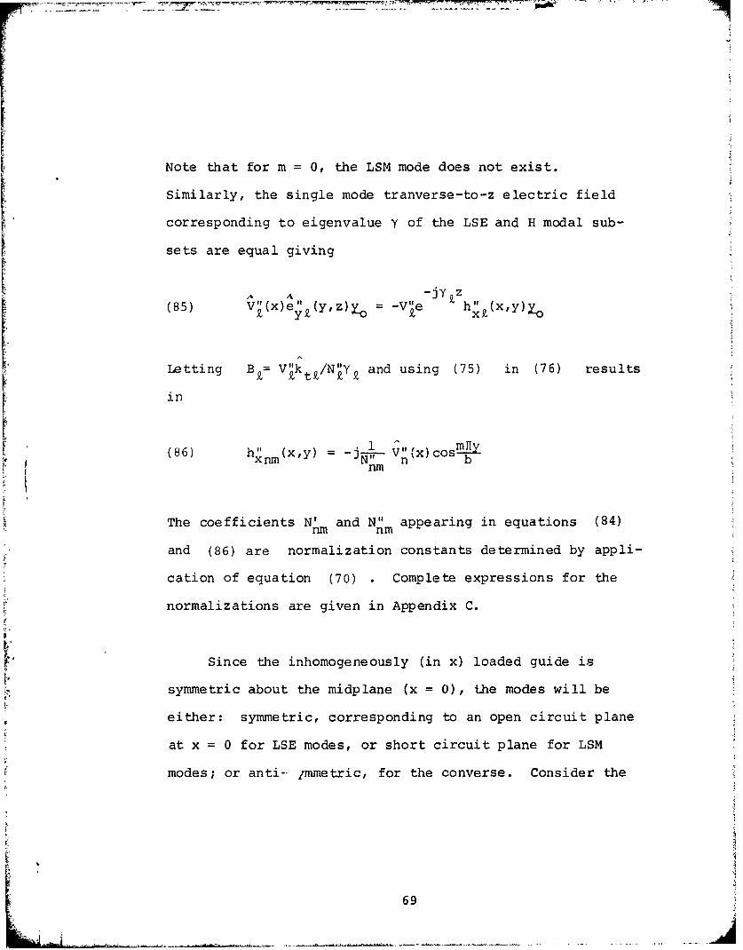
Note that for m = 0, the LSM mode does not exist.
Similarly, the single mode tranverse-to-z electric field
corresponding to eigenvalue y of the LSE and H modal sub-
sets are equal giving
j'y zVII!
(85) V (x)e (y,z) o = -Vie hx (X,Y)yo
Letting Bk= V kt /N"Y £ and using (75) in (76) results
in
(86) h" (x,y) = j V"x)cosxnm- nbnm
The coefficients N' and N" appearing in equations (84)nm nm
and (86) are normalization constants determined by appli-
cation of equation (70) • Complete expressions for the
normalizations are given in Appendix C.
Since the inhomogeneously (in x) loaded guide is
symmetric about the midplane (x = 0), the modes will be
either: symmetric, corresponding to an open circuit plane
at x = 0 for LSE modes, or short circuit plane for LSM
modes; or anti-- Immetric, for the converse. Consider the
69

equivalent transmission line representation of wave propa-
gation in x shown in Figure 27. The complete current and
voltage distributions may be written down by inspection for
either of the indicated terminations. The resultant
distributions are then appropriately inserted in (84) or
(86) to obtain the cross-sectional dependence of the
x components of LSM dlectric and LSE magnetic mode functions.
The vector mode functions are summarized in Figures 28
and 29.
In normal operation as a dual frequency phased array
element,the excited (propagating) modes of the symmetric
twin dielectric slab loaded rectangular waveguide will be
the LSE 10 mode in the low frequency band, and LSE1 0 and
LSE 20 modes in the high frequency band. At either band,
the tendency will be for the field strength interior
tc the dielectric slabs to exceed the field strength
elsewhere. This characteristic is clearly evident in the
equations of Figure 29 for slow wave propagation. Exam-
ination of the modal voltage expressions shows that for
K = - n e"l0(x,y) is propoitional to cosh(IKnx l) inn cn.(I Y10)°-<x<O, and to sinuh IK nl (x+a/2) in -a/2<x<-6-6. Thus,
for greatly slowed waves, i.e., PM k Vr, the
e" (x,y) is nearly exponential in the air regions, andyl0nearly constant in the dielectric. Sim.ilar characteristics
70

Sc oc/3/2 OR OR
0 li F 1~ _____ PC PMC
-A /21
Figure 27. EqiaetTasiso Line RepresentationoA aePropagation in x.J
- - -71
~' 21
x XV vA
V N
V + N
I- w H
0)0
>1 1
N -.4
N4 >1
-U) 0
(H ~ -27 "Nv
XNv
v
I .4
m
U0)
'N
ve lli
+ 2: x ' t
Q) v- .1 a) j I44 -1
E-N -
I 4 Ff C
H ~ '-4

0 v '0
v
vx x
v I
XN C-
O) ca 1-
0+ co
v 0
W Iz4 U) w
>1 I -.
x Q)
I II
C C.)0
a) ) ca -
c.i
54 U)H
H 7 +

a.e evident for the LSE20 mode (the first anti-symmetric in
x mode).
Typical e" (x,y) distributions are shown in Figuresy10
30 and 31 for an element operating at 2.5 GHz and 6.0
GHz, respectively. The element is a WR187 guide with .250"
(=6) slabs of er = 9 dielectric located .325" (=-a) froin.
either narrow wall. At low frequency, the distribution is
roughly uniform between slabs, with some field concentration
in the vicinity of the interior air-dielectric interfaces.
In the region Ixl>8+6, the field behaves very nearly like
cos(]lx/A). At 6 GHz, the e'yl0 (x,y) distribution is entirely
different, showing well defined field concentration about
the dielectric, with very low field strength in the air-
filled regions. The distributions are roughly symmetric
about the slabs, with non-zero field at the guide center.
As the dielectric constant is increased the fields become
more heavily concentrated in the dielectric, and, consequently,
the field strength at the guide center approaches zero.
At 6 GHz, the antisymmetric LSE 20 mode is also propa-
gating, and all other modes are well beyond cut-off. The
e" (x,y) distribution is shown overlayed on the e" (xy)y20 yl0
distribution in Figure 32. This comparison shows that the
74

I
0.8-
. 0.6 - -
: ~~0.4 I i'
Z SLA BS, E r 9 ..0.2-
I
-0.5 -0.4 -0.3 -0.2 -0.1 0 0.1 0.2 0.3 0.4 0.5
,VA
Figure 30. eyl0 (x,y) Distribution for WR187 Bifurcated
Guide With .250" Thick E = 9 Loading. 2.5 GHz
75

: ~ ~1.0 Ii I
I I I IIII I
0.8- _ -
-Ju __ I __u- 0.6-
0
oI I_ i _
o.2- ,I .. ___.._DIELECTRIC -I ~~~SLA SI
-0.5 -0.4 -0.3 -0.2 -0.1 0 0.1 0.2 0.3 0.4 0.5Ki'A
k
Figure 31. eyl 0 (x,y) Distribution for WR187 Bifurcated
Guide With .250"Thick Er = 9 Loading. 6 Gllz
76

1.0--DIELECTRIC
0.8-- ~SLABS, 16=90.8 -I/ _ - - " - _ _
LU- _ _ _ A .
U" 0.6 •-- ; -
LU IN _
0.4 r--
2 , - /LSE 20 I I0.2- : I_ ._ ;e- / , I
0 1v-0.5 -0.4 -0.3 -0.2 -0.1 0 0.1 0.2 0.3 0.4 0.5
/A
Figure 32. ey1 0 and ey2 0 (x,y) Distributions for WR187 Bifurcated
Guide With .250" Thick fr = 9 Loading. 6 GHz
77
A
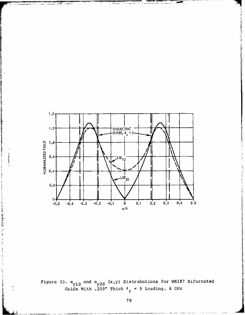
LSE and LSE20 modal field distributions are quite similar,10 2
differing by no more than a few percent in relative magnitude
for jx/Al>.15, but having opposite symmetries. It is
this high frequency propagation characteristic and the fact
that 20 /y10 -1.0 for appropriately chosen dielectric
constants and guide geometries which provide the unique
dual frequency array element potential of the symmetric
twin dielectric slab loaded rectangular waveguide. For,
assuming the functions are exactly identical in magnitude
and that y20/yI0 = 1, the LSE10 and LSE20 modes, by
magnitude control only, may be excited such that two in-
dependent phase centers are located at roughly the positions
of the slabs.
The similarity of the e" (xy) and e" (xy) dist-y10 y20
ributions, and hence, the achieveable high frequency phase
center independence, is directly related to dielectric con-
stant for fixed geometry. As the dielectric constant is
decreased, holding cross-section fixed, the LSEI0 distri-
bution approaches the TEl0 distribution of empty guide;
and the LSE20 approaches the empty guide TE20 distribution.
These trends are evident in Figure 33, where the e" (x,y)yl0
and e" (x,y) distributions are shown overlayed for the~y20
WR187 guide with r = 5 loading. The departure in magnituder
78
1.0- DIELECT'RIC I--SLABS, f =5 1
N 0.6- / LSE1 ILSE 20
0.2--1K
-0.5 -0.4 -0.3 -0.2 -0.1 0 0.1 0.2 0.3 0.4 0.5x/A
Figure 33. e and e (x ,y) Distrubutions for WR187 Bifurcated
Guide With .250" Thick 1E =5 Loading. 6 GHzr
79

between the distributions is significantly greater for the
lower dielectric constant than for the higher.
While the above discussion shows that there is a strong
influence of dielectric constant on achieveable high freq-
uency phase center independence, it should not be construed
that large dielectric constant is generally preferable to
low dielectric constant. In particular, it will be shown
in section 4-1 that for certain geometries, dielectric
constants on the order of c = 9 may lead to large aperturer
reflections which are difficult, if not impossible, to
match outJ
80

3.2 Mode Spectrum
The modal spectrum of the symmetric twin dielectric
slab loaded rectangular waveguide is obtained via a
transverse resonance procedure. Representing the loaded
guide as an E or H mode transmission line in x, as in
Figure 27, and requiring that x = 0 be either an open or
short circuit plane results in four dispersion relations,
in x, of the form,
(87) D(K nK n) =0.
where
(88) K2 k 2 - mU 2n B nm
(89) K = K2 + k 2 (e -1)Fn n n r
k = 2H/X is the free space wave number, mH/B is the y
directed wave number, and Ynm is the z directed wave-
number. One dispersion relation is obtained for each
symmetry condition, in x, of each modal subset. The
four dispersion relations are given in Table 2. It
should be noted that the forms given are computationally
unstable due to both the various tangent evaluations,
81

w coW 4')00
V. V 4J s )sz4J 01
w v 0 S! V -J 'V 0
lz St p U + v w41) U sz St 0 + sz U)
Vt se I r 4 4J W ( C : :3- S4c w U) ( v S4 m 0
w v + sz r. V
se S4.) W l
+ s- 4.1+++ +
.+ t I
0 0)%>
"44Stse 41) 4.)
5.1 U) w 4.4
uU 0
xx5.4 5-4 A4 z
0 0 0 0 5-I
0 ;04-) U)
U) U
00uH
0 00.r4 -44
4.34
>13
C) U1) V
82

and the indicated divisions. -n-practice, the expressions
are converted to combinations of sines and. cosines, and all
divisions are removed.
In the LSE and LSM modal subsets, the mode indexing
is (n,m). The first index, n, is associated with theinfinite sequence of zeros of D(K,K € which are arrayed1
along the real K axis, as illustrated in Figure 34.
The first zero is always associated with the even symmetry
solution of the modal sub-set (i.e. open circuit symmetry
for LSE modes; short circuit symmetry for LSM modes).
Thereafter, the roots of the even and odd symmetry disper-
sion relations are interleaved. Hence,for even symmetry,
n is always odd, and conversely. The second index, m,
appears explicitly in the auxilliary dispersion equation,
(88), and is directly interpreted as the order of the y
variation of the modal field.
The potential of the symmetric twin dielectric slab
loaded rectangular waveguide as a dual frequency array
element arises, in part, due to the unique migration of the
roots anu Y20 with frequency. Figure 35 shows an
LSE mode dispersion diagram for half height WR187 guide
with c = 9 loading. Only the (n,o), n = 1,2,3 and (n,l),
n = 1,2 roots are shown, other LSE roots being considerably
83
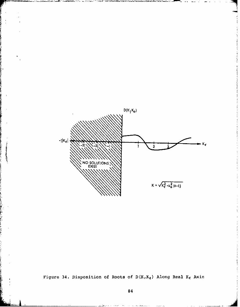
D (K Kd)
SNO SOLUTIONS
, EXiS
!: Figure 34. Disposition of Roots of D(K,K e) Along Real Ke Axis
484

10.00,
A X
8.*00 -6.00-
4.00-- V=k
Cq
PROPAGATING
EVANESCENT
-2.00 .a/13 1.000J /A = 0.1335
= 9.00-4.00 '
1.0O0 1, 50 2.0O0 2.50 3, O0 3.50 4.0
KA/2
Figure 35. LSE Dispersion Diagram for BifurcatedWR187 Guide With 250" Thick r = 9 Loading
85
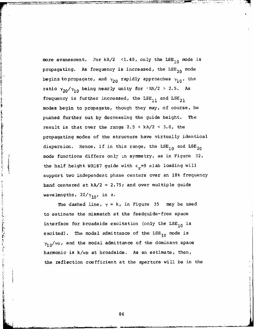
more evanescent. For kA/2 <1.40, only the LSE 10 mode is
propagating. As frequency is increased, the LSE 20 mode
begins topropagate, and y20 rapidly approaches yI0 , the
ratio 720/710 being nearly unity for 'IKA/2 > 2.5. As
frequency is further increased, the LSE 11 and LSE21
modes begin to propagate, though they may, of course, be
pushed further out by decreasing the guide height. The
result is that over the range 2.5 < kA/2 < 3.0, the
propagating modes of the structure have virtually identical
dispersion. Hence, if in this range, the LSE 10 and LSE20
mode functions differs only in symmetry, as in Figure 32,
the half height WR187 guide with E r=9 slab loading will
support two independent phase centers over an 18% frequency
band centered at kA/2 = 2.75; and over multiple guide
wavelengths, 2l/yl0 , in z.
The dashed line, y = k, in Figure 35 may be used
to estimate the mismatch at the feedguide-free space
interface for broadside excitation (only the LSE 1 0 is
excited). The modal admittance of the LSEI0 mode is
Y1 0 /wp, and the modal admittance of the dominant space
harmonic is k/wU at broadside. As an estimate, then,
the reflection coefficient at the aperture will be in the
86
neighborhood of
=Y1 -k
(90) r ~ +----
for broadside excitation. For the WR187 guide with Fr=9r
loading, operating at KA/2 = 2.99, equation (4-39) gives
SFl = .383, whereas the exact value for a rectangular thin
wall array of these guides is IFl = .424. For the same
guide operating at kA/2 = 1.25, equation (90) gives
1'1 = .110, and the exact value is Il = .285. In both
cases, the implication is that the aperture susceptance,
which is ignored in (90) , is significant. This is not
entirely surprising, since it is well known* that equation
(90) is exact for thin walled rectangular grid arrays of
empty rectangular grid guide, for which the set of trans-
verse wavenunmbers of the feedguide is the set of transverse
wavenumbers for the unit cell guide.
For fixed guide wall dimensions, the parameters which
most strongly influence the dispersion curves are dielectric
constant and slab thickness. The location of the slabs,
denoted by the ratio ot/3, has second order effects in the
regions .5< c/3 < 2.0. c/B ratios outside this region are
not of interest due to the irregularly spaced high freq-
*See, for example, Amitay, Galindo, and Wu,(10) pg 132ff.
87

uency phase centers which would result.
Figures 36 theough 39 -re LSE dispersion diagrams
for half height WR137 guide with 6 = .250" and a/a = 1.00.
The curves progress from loading of r=3 to cr=9 . As the
loading increases, y20 approaches yl0 , in general, and the
trend is toward steeper slopes.
The migration of the LSE30 cutoff frequency toward
lower frequency produces one of the critical trade-offs
inherent to the design of the symmetric twin dielectric
slab rectangular waveguide dual frequency array elerent.
In general, the overriding array design criterion will be
to minimize the number of radiators (or, equivalently
maximize array cell size). Thus, for dual frequency
operation, the high frequency band center operating point
will be in the vicinity of kA/2 = 1. In this region,
the higher dielectric constants (er = 7,9) provide y2 0 /y 1 0
ratios very close to unity, but the LSE30 mode is propa-
gating. Since it is necessary to push this mode out, lower
dielectric constant is required.
Similar results are obtained by holding cr fixed and
varying only slab thickness, 6. Figures 40 through 43
are LSE dispersion diagrams for four slab thicknesses in
half height WR137 guide. The dielectric constant is 5,
and a/ = 1.00. In general, the behavior with thickness
L ~ 88

U;
Li;
I] 502-U 2~D3.00 35
E- .5.0
LEISENMM LSE0100 + LSE00X LSED300 4* LSE0102.
bLS5ED201 LSED3012
Figure 36. LSE Dispersion Diagram for BifurcatedWR137 Guide With 250." Thick E r =3 Loading
89

U
ru
=D=
.000
#,-- .3.25:2
/ ' , -. ,
LEIENM
M LSED1DD + LSED2DX LSED300 LSE01D1b LSED201 LSED3D1
Figure 37. LSE Dispersion Diagram for BifurcatedWR137 Guide With .250" Thick er = 5 Loading
90L.

a
m
KR/2
C3
C!
:r" Lf=DK
E-7.00
LENMMj LSE02.00 + LSE0D0X LSED300 4, LSE01OI.t LSED201 16 LSED3D)1
Figure 38. LSE Dispersion Diagram for BifurcatedWR137 Guide With .250" Thick E 7 LoadingL....91

3 /
71, K
IND Sv q K
K," ;Li;
pJ
9.0
LECiEN'Mt LSlllrml3 + LS.ED2'
X LSEr3D0 t, L.EO'ID1SLSE02O1 6 LSED3D1
Figure 39. LSE Dispersion Diagram for Bifurcated
WR137 Guide With .250" Thick e = 9 Loadingr
L92

C2K
IVD
IUI.Su 2.111 d.sa i4iUU45 4
:L.ODDi/R .34-9
M LSE0100 + LSE13DDX LSE1300 q, L5E02.D2t~ LSE0202. LSED301
Figure 40. LSE Dispersion Diagramr for BifurcatedWR137 Guide With .063" Thick er 5 Loading
93

It
soU o i
LEMEN1SLE0lO + LSE0200
x LSEI1300 *L5E0101oj LSED201 a) LSED301
Figure 41. LSE Dispersion Diagram for BifurcatedWR137 Guide With .125" Thick Er 5 Loading
L 94

ta
an
F:I-
LaED20 ejsfLS 31
F
Fp I, .- r a
LEBN.Uj L.5ErIr.I + LS~rD2.31)X L.5E051r2 , LSEI.0L ,
qI L.5Er22DL3] L.SLI3m1Ji
~Figure 42. LSE Dispersion Diagram for' B.ifurcated
WR137 Guide With .188" Thick Er = 5 Loading
95

AkVC3
C2
CSC2 y=
a J
CC2
2
rq
L= ,ZT33
wLSESD201 LSED301
Figure 43. LSE Dispersion Diagram for BifurcatedWR137 Guide With .375" Thick er 5 Loading
L 96

is very like the behavior with e However, comparison
of Figures 39 and 43 shows that high dielectric
constant is preferable to extreme thickness. In the two
figures, the LSE30 mode enters at roughly the same freq-
uency, but the ratio of z directed wave numbers, /Y10,
is significantly nearer to unity for e r=9 than for
Cr=5.•
ir
t
I
97

4,0 ARRAY APERTURE DESIGN
In this section, the trade-offs leading to a
practical array aperture design are presented for the
hypothetical array performance given in Table 3. The
operating bands are 15% centered at 4 and 8 GHz. Sixty
degree (600) principle plane scan coverage is required.
The array is to provide 30 db gain for 600 principle
plane scan at 4 GHz. The first sidelobe level is to
be below 20 db and RMS sidelobe levels are to be below
35 db. Nominal feed losses of 1.5 db at 4 GHz and 2.8
db at 8 GHz are assumed. To reduce the inherent
difficulties in matching out the aperture, an aperture
mismatch loss at broadside of no greater than .6 db
is required.
To provide the required performance, a Taylor,
n=3, 25 db SLL distribution is selected, resulting in
an aperture gain of 37 db at 4 GHz.
The principle result of this section is the
X determination of an element/grid configuration which
minimizes element count while holding high frequency
grating lobe contributions to levels consistant with
the sidelobe requirements.
98

Frequency 4,8 GHz +7.5%
Scan Coverage +600 in either principle
plane
Aperture Gain @ 600 30 db @ 4 GHz
Principle Plane Scan
1st Sidelobe Level 20 db
RMS Sidelobe Level 35 db
Feed Losses 1.5 db @ 4 GHz
2.8 db @ 8 GHz
Aperture MismatchLoss@ 0° Scan <.6 db in both bands
Table 3
Prescribed Array Performance
99

4.1 Aperture Design Trade-Offs
It is well-known (1 6 ) that an equilateral triangle
lattice configuration minimizes element count for a
given scan requirement. As a basis for comparison,
it is therefore, convenient to first consider a lattice
specifically taylored to minimize element count at
low frequency. This lattice and the near-in grating
lobe diagrams for 4 and 8 GHz are shown in Figure 44.
The lattice base is 1.780" (.602X @ 4 GHz).
It is immediately apparent from Figure 44c that
the six near-in high frequency grating lobes will
migrate well inside the coverage sector for all scan
directions and pose a potential limitation on achieve-
able peak sidelobe level and main beam gain. This
difficulty may be alleiviated somewhat by appropriate
selection of the element configuration and high freq-
uency excitation modifier, R, for the LSE 2 0 mode as
discussed in section 2.2. However, it should be noted
that the six grating lobe locations actually represent
twelve independent beams (six each E and H with respect
100

. 7 7 0,1.8 9 o " -
0 0
------- - I11.0ft0 0 0 0
x x0 0 j0 0
--1 .780"- - -
(a) Lattice\Configuratlon Shown Low (x) andHigh (o) Frequency Centers
V/K V/K22(0, 1)
(-1, 0) ( , 1)0 0011)
u/K 1u/K-2 1.1 2 -
((- ),(-,I)
(-I, - 1) -2
(0 , -1 2-2
(b) Low Frequency Grating Lobe (c) High Frequency Grating LowDiogro -/ox ,. 6 6 ,X/v, :1.92 Di'gay .- 6
Figure 44. Equilateral Triangle Lattice ConfigurationWhich Minimizes Element Count @ 4 GHz
101

to the array normal). Since there are only nine design
parameters (half aperture dimensions A and B; septum
thickness; 6; relative permittivity, e; slab thickness,
F6; ratio a/a; lattice spacings, dx and dy; and R), it
is clear that there is insufficient control for the
cancellation of all beams.
The only available means of cancelling the beams
residing al.ong the v axis, the (0,1) and (0,-l) lobes
is to separate the half apertures by one half the y
lattice spacing dy, resulting in a scanning sub-array
pattern with nulls coincident with the grating lobe.
This coincidence is maintained for H-plane scanning,
however degrades in all other scan planes due to the
imbalance in half-aperture reflections induced by the
phase taper. In the circumstance that the half aper-
tures are spaced at less than 0.5 dy, a significant
fraction of the radiated power is delivered to the
E-mode (0,1) and (0,-l) beams for all scan directions,
including broadside. In calculations with the half
apertures separated by 0.26 dy, it was found that as
much as 20% of the power was delivered to each of the
two E-mode beams at broadside scan.
L/ 102
Cancellation of the remaining eight beams is a
considerably more difficult problem, and turns out to
be virtually impossible for this large lattice spacing.
Again, effective reduction of radiated power into the
unwanted lobes must be obtained by locating the null
of a scanning subarray pattern at or near the grating
lobe location. One subarray spacing has already been
used to cancel the on axis lobes; the remaining degree
of freedom is therefore, the x separation of the appar-
ent high frequency phase centers. In the event that
these separations can be extended to 0.5 dx , good grating
lobe rejection can be achieved. However, as a practical
matter,such wide x displacements of apparent high freq-
uency phase centers are not possible.
As was shown in section 3.2, a reasonable upper
limit on aperture x dimension is in the vicinity of
A=A at the center of the high frequency band for moder-
ate relative permittivity loading (Er =5). Largerr
aperture dimensions can be achieved by reducing the
permittivity, or using very thin slabs; however, such
an approach is generally counter-productive in that
bandwidth is reduced and H-plane scan loss is increased
at high frequency due to the widening dissimilarity
L 1 103
between LSEo and LSE2 o modes which occurs for parameter
variations in these directions. Consequently, in order
to achieve the wide apparent phase center displacement
for this grid, it is necessary to place the slabs
very close to the narrow feedguide walls, giving a/8
ratios of, typically, 0.56 to 0.62. This is not a
very attractive solution since it produces considerable
aperture field asymmetry about the apparent phase
centers, thereby invalidating the primary assumption
that the high frequency aperture distributions are
roughly symmetric about these phase centers. As a
practical matter, then, it is impossible to kill off
the eight remaining beams.
The best result obtained for the 1.78" base
equilateral grid are summarized in Table 4. The
element dimensions are given in the table caption.
Clearly, the 1.05 db power loss to the grating lobes
is intolerable, and it is necessary to reduce the grid
size significantly.
As mentioned above, cancellation of off-axis high
frequency grating lobes requires that the aprparent
phase centers be separated by roughly 0.5 dx. In
addition, to maintain reasonable aperture field symmetry
about these phase centers, ratios a/g should lie in
the approximate range 0.8 < a/$ < 1.25. Allowing for
104

4 GHz 8 GHz
Broadside Reflection Loss (db) 1.18 1.05
*H-plane Scan Loss at 600 (db) 6.44 6.80
Power Loss to Grating Lobes
(broadside scan) 1.05
Broadside Gain Loss (db) 1.18 2.43
Table 4
Performance of Dual Frequency Element in 1.78" BaseEquilateral Traingular Grid at 4 and 8 Gaz. A = 1.480",
.412", 358", dx = 1.780", d = 1.540", a- .241",= 301", = .198" = 5.0
*Includes cos e beam broadening factor.
105

a wall thickness of 0.062", a practical set of element
and grid x-dimensions is then A = 1.376", dx = 1.500",
and 0+6/2 = .375", resulting in the specification of
slab thickness, 6, as no greater than .130", or
6/A<.094 and a/$<.835. From Figures 36 through 43,
it is seen that a relative permittivity of 5 will
provide the desired feedguide characteristics in both
frequency bands for this aperture size with c/ = 1
and 6/A = .091. Bringing the a/$ ratio into the
required range produces only a small perturbation
on the dispersion curves shown in Figure 41. Consequent-
ly, the selection of a=.247", 0=.309", and 6=.132"
will provide the necessary control of off-axis grating
lobes while keeping higher order feedguide modes well
below cutoff. By requiring that the LSE 11 mode be
attenuated by 8 db per wavelength at the high end of
the 8 GHz band, the y aperture dimensioned is obtained
as B = .400".
The aperture/grid parameters determined so far
guarantee some cancellation of the off-axis grating
lobes, and it might be assumed that by reducing dy
for the original grid by the ratio 1.5/1.78 would
result in an acceptable configuration, giving a 29%
- 106

increase in element count over the "optimum" number.
Unfortunately this spacing is still on the large size
and results in considerable power loss to the grating
lobes at relatively small scan angles. It is there-
fore, necessary to further reduce the cell along the
E-plane to dy = .960".
The final configuration, shown in Figure 45,
with its low and high frequency grating lobe diagrams
has a cell area roughly half that for the grid optimized
for element count at low frequency, and results in an
array of 2444 elements. With five phase shifters per
element, this increase seems (at first glance) rather
unattractive. However, this comparison is quite mis-
leading. The twin dielectric slab dual frequency array
element concept provides for simultaneous excitation
by two entirely independent feed systems, and con-
sequently the simultaneous radiation of two indepen-
dent beams at two widely separated frequency bands.
If the alternatives for multifrequency operation are
considered, the dual frequency element is suddenly
very attractive.
One such alternative is the use of wideband
elements in the grid depicted in Figure 44 to obtain
simultaneous aperture usage. The obvious disadvantage
107

1 .500"
0.618"
0.247"- 0.132"
0.132"- 0.2471"
00.40
(a) Element/Grid Configuration
V/K3(01
2 20(-1, O') 0(1,1)1
F- u/K-2 1 -2 -11 2
00 0)
(0, -1)
(b) Low Frequency Grating Lobe (0)High Frequency Grating LobeDiagram /DX=1.96X/Dy: 3.07 Diagram -XDXx -98, X/Dy= 1.54
Figure 45. Triangular Grid Configuration for Dual FrequencyOperation over 16% Bands Centered at 4 GHz and 8 GHz
108

of this scheme is that it requires eight phase shifters
and four diplexers per element quartet or unit cell.
In comparison with the dual frequency element, this
configuration requires twice the number of low freq-
uency controls, and half the number cf high freq-
uency controls per unit area of the array, plus di-
plexers.
A second alternative, in a broad sense, is to
design two entirely independent single frequency
systems. However, it is clear that only under very
special circumstances could this system be considered
a viable multifrequency concept.
j Predicted principle scan plane performance for
the configuration in Figure 45, is shown in Figures 46
through 54, at the end and midpoints of the 4 and 8
GHz bands. In these figures, the performance measure
is taken as the power transmission coefficient int.-
the radiating beam(s). Mainbeam scan loss is deter-
mined by adding 10 log1 0 (cose) to the curve for the
(0,0) beam.
Figures 46, 47, and 48 show E and H plane per-
formance at the low end, middle, and high end of the
4 GHz band, respectively, for scan out to sinO=.975.
109

-5
" -100
z
0 --15-
,z
LU -20*
0
-25
-30
0.00 0.20 0.40 0.60 0.80 1.00
- SIN e0
F = 3.68GHz A = 1.376in.a = 0.247 in. B = 0.4001n.
IB = 0. 3 09 in. Cx = 1.560 in.
6 = 0.132in. Cy = 0.960in.
= 5.0 SEP = 0.032 in.
CUT PLANE SINO = 0.000
LEGEND
6 H-PLANE-- E-PIANE
Figure 46. E- and H-Plane Performance of Designed Element,f =3.68 GHz
110
L -Al .. ... ... . . . .
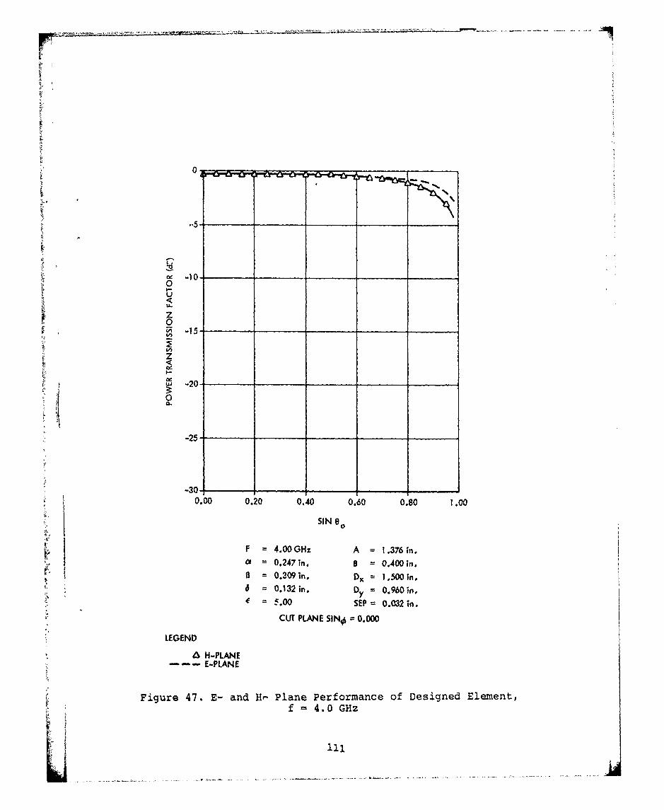
0.
" -I 0 . -.....-
(. ~ -10-0U
z0
z
-20,
0
-25-
-30 .. .0.00 0.20 0.40 0.60 0.80 1.00
SIN e 0
k F = 4.00GHz A = 1.376in.
= 0.247 in. 8 = 0.400 in.3 = 0. 3 09in, Dx = 1,5001n.
= 0.1321n. D = 0.960in,= f.00 SEP= 0.032in.
CUT PLANE SINO = 0.000
LEGEND
a H-PLANEE-PLANE
Figure 47. E- and H,- Plane Performance of Designed Element,f 4.0 GHz
il

-5-
S-100
z0
Ui -20-
0
-25
0.00 0.20 0.40 0.60 0.80 1.00
SIN 80
F= 4.32 GHz A =1 .376 in.
=i 0.247 In. B 0.400 in.
000 =n 1 .500in.= 0.30in. D x 0.960 n.
£= 5.00 SEP =0.032 in.
CUT PLANE SINO 0.000
LEGENDa H-PLANE
~-.-E-PLANE
Figre 8.E- and Ii- Plane Performance of Designed Elemenlt,
Figue 4f =4.32 Gliz
112

F4
0<
-5
-10
0" -15
z 20
I'U-20
-25
-30
-35.0 0.20 0.40 0.60 0.80 1.00
SIN 00F = 7.36GHz A = 1.376in.
i= 0.2 47 in. B = 0.400 in.
3 = 0.309 in. Dx = 1.5001n.
6= 0.132 in. Dy = 0.960 in.= 5.00 SEP = 0.032 in.
CUT PLANE SINO = 0.000
LEGEND
6(0, 0, 2)0 (H, -1 , 2)O (-1, -1, 1)
Figure 49. Propagating Beam Power Levels - H-Plane Scan,
f = 7.36 GHz
113

-5
0
-10,
0
U. -15z0
Z -20,
I-
0 -25-
-30-
0.00 0.20 0.40 0.60 0.80 1.00SIN eo
F = 8.00GHz A = 1.376 in.= 0.247 in. B = 0.400in.
B = 0.309 in. Dx = 1.500 in.6 = 0.132 in. Dy = 0.960in.
= 5.00 SEP = 0.032 in.CUT PLANE SIN = 0.000
LEGENDZ (0, 0, 2)0 (-1, -1, 1)O(-2, -1, 2)
Figure 50. Propagating Beam Power Levels - H-Plane Scanf = 8.0 GHz
114

-10-
z
Z -20-
04 -25-
-30-
0.00 0.20 0.40 0.60 0.80 1 .00SIN eo
F -8.64 GHz A 1 .376 in.cc= 0.247 in. B 0.400 in.
B 0.309in. Dx 1 .500Gi.6 0.132 in. D y 0.960 i.
E =5.00 SEP 0.032 in.
CUT PLANE SINO= 0.000
LEGEND
6 (0, 0, 2) o (-1,-1, 1)
Figure 51. Propagating Beam Power Levels -H-Plane Scan,f =8.64 GHz

SI
-5
-10-0U-
0, -15
S -20
0
-25-
-30.
0.00 0.20 0.40 0.60 0.80 1.00
SIN e0F = 7.36GHz A = 1.376 in.
G = 0.247 in. B = )0.4 0 0 in.
1= 0.309in. Dx = 1.500in.
= 0.132in. Dy = 0.960in.c = 5.00 SEP = 0.032 in.
CUT PLANE SIN =1 .000
LEGENDA (0, 0, IN
O (0, -1, 1)
Figure 52. Propagating Beam Power Levels - E-Plane Scan,f = 7.36 GHz
116

-v
0
ML. -15-
0
22
-25-
0
-30'-
-35.0 0.20 0.40 0.60 0.80 1.00
SIN 0,
F = 8.00GHz A = 1 .376 n.= 0.247 in. B = 0.4 00 in.
(3 = 0.309 in. Dx =i1.500 in.6 = 0.132 in. Dy = 0.960 In.
= 5. 00 SEP = 0.032 in.
CUT PLANE SINO 1.000LEGEND
a (0, 0, 1) 0(0,-1, 1)0 (1,-,1 0(-,-,2
Figure 53. Propagating Beam Power Levels -E-Plane Scan,f =8.0 GHz
117

-5=
,- -10. -i
0I-i
z0
z< I
LU -20-..
-25-
k ~-30 ..0 0.20 0.40 0.60 0.80 1.00
SIN e0
F = 8.64GHz A = 1.376in.
Of = 0.247 in. B = 0.400 in.
B = 0.309 in. D, = 1.500in.
6 = 0.132in. D = 0.960on.
e = 5.00 SEP = 0.032 in.
CUT PLANE SINfO = 1.000
LEGEND
6 (0, 0, 1n 0(0,' -1, 1O (1, 1, 0 (-],, 2)
Figure 54. Propagating Beam Power Levels - E-Plane Scanf = 8.64 GHz
118
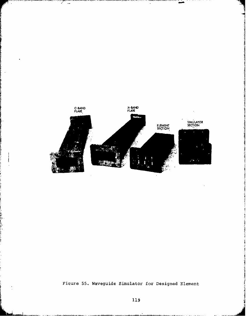
C- BAND X- BANDFLARE FLARE
ELEMENT SECTION' ~~SECTION...'
/3
119
Ii1
Fique 5. Wvegide imuato fo Desgne ElmenI,
119
C-ADXBN -I= = = ..

In this range, no grating lobes enter real space. Maxi-
mum broadside mismatch loss in this band is less than
.3 db and is readily matched out by any number of means.
The E-plane fall-off out to approximately 60 is some-
what better than might be expected for the subarray
array factor at these spacings, and decreases at the
upper end of the band. The H-plane fall-off is typical
of a planar array of rectangular apertures.
Figures 49, 50 and 51 show the H-plane power levels
in the propagating beams in the 8 GHz band. To eval-
uate the array characteristics over this band, the LSE10
and LSE2o feedguide modes are assumed to be generated
2 Xg10 behind the aperture plane, where Xgl1 is the
LSEio guide wavelength evaluated at 8 GHz. This long
feedguide phase length results in considerable excita-
tion of the (-l,-l) E-mode at the band extremes. Evi-
dently, this path must be shortened for such wide band
opexation.
At midband, Figure 50, the (-l,-l) and (-1,0)
grating lobes are well within the desired range of rms
sidelobe level and will not result in any significant
perturbation of the far-out sidelobe region. This
120

level of cancellation is achieved using the modifier
R - 1.2 exp ( -j14 O ), which seems to also result in
significant reduction of the H-mode (-1,-i) and
(-1,0) beams at the band edges as seen in Figures 49
and 51. However, the modifier clearly has little
effect on the E-mode beams, and these levels must be
controlled by a proper choice of a feedguide phase
length.
In Figure 51, it is seen that the (-2,-l) H-
mode beam is heavily excited at the upper end of the
band. However, this occurs only at the H-plane
extreme of the scan volume, and will be of only minor
consequence.
The 8 GHz band E-plane performance is shown in
Figures 52 through 54. In general, the best perform-
ance occurs at the lower end of the band. Due to the
choice of y lattice spacing, the grating lobes remain
outside real space throughout most of the scan volume
at this end of the band, and are only moderately
excited upon entering. From the results at 8 and 8.64
GHz, it is clear that this is the most effective means
of controlling spurious beam levels in this plane.
Ai the high end of the band, the (-l,-l) E
and H imocte beams are very heavily excited and will
121
L .. . ii

I
have considerable impact on the general sidelobe level
for scanning beyond 250. However, except for the small
dips occuring near (-1,-i) lobe incipience, there is
little effect on main beam gain. Again, as for the
H-plane results, a general improvement in grating lobe
levels may be expected for shorter feedguide phase
lengths.
4.2 Experimental Evaluation of the Bifurcated Twin
Dielectric Slab Loaded Rectangular Waveguide
Dual Frequency Element
The dual frequency element design shown in
Figure 45 was built and tested in H-plane waveguide
simulators over an 8% frequency band centered at 4.6
GHz and a 16% band centered at 8 GHz. In general,
the experimental results were in excellent agreement
with predictions.
The simulators are shown in Figure 55. They
are constructed of brass and are soft soldered. A
single element section and parallel wall simulator
section is used for both bands, resulting in near broad-
side simulation in the upper band, and wide angle scan
simulation in the lower band. The parallel wall
section has 2.250" x .960" cross-section and provides
imaging as shown in Figure 56. In the low frequency
band, only the TEio mode propagates in the simulator.
In the high frequency band, up to eight modes can propagate.
L 122
Ll.
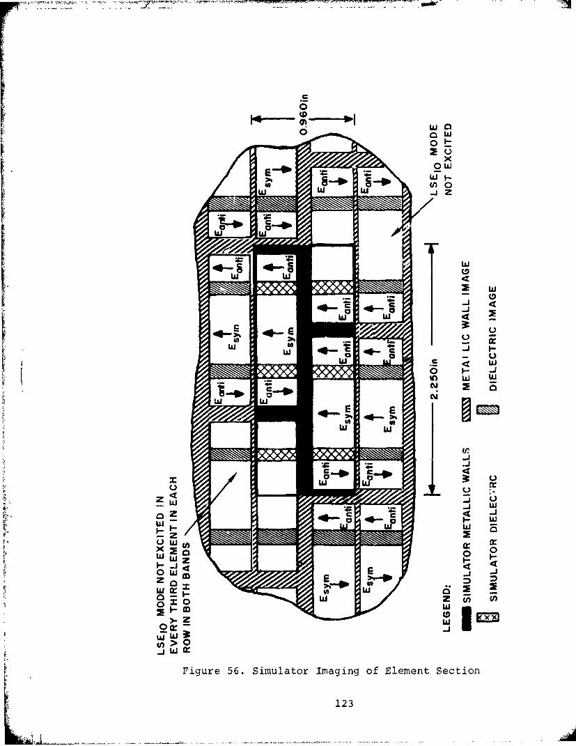
.S0
1 oUI
(A 0Ui~. 4 j
t0
41*. GE000,0;- U
(jj
E e
cc
-Z
L)w xa 0
ZO
0 ~ u
Figure 56. Simulator Imaging of Element Section
123

0 0K 0 It O
~ F..J4.24
432 TTX
Samle in8ts Iceet
124
-0- ..... 71 "77 - 777
The element section, shown in Figure 56 with tPe
simulator imaging, consists of two half elements and
two cuarter elements, resulting in 19.10 and 410
H-plane scan simulations at the centers of the high
and low bands, respectively. The dielectric slabs
are stycast HiK, Er = 5. The element section is 7.2"
long (2A at 4 GHz), with tapered 3.6" 3000 cardg
loads inserted at the rear of the section on either
side of the dielectric slabs and the feedguide mid-
plane. The long tapers are necessary to eliminate
rearward radiation and reduce reflections at the load
discontinuitie s.
Figure 57, shows measured results in the upper
half of the low frequency band. Results in the lower
half of the band were not obtained due to the freq-
uency limitation of the network analyzer. To ensure
measurement accuracy, the experimental band was
sampled discretely in 80 MHz increments, and a short
circuit reference was established at each frequency
step. Measured reflection coefficient maqnitude is
in the rance .34 to .41* with the peak and minimum
at 4.24 and 4.08 GIz, respectively, and is typical of
the variation in H-plane gain loss with scan observed
in many broaaside matched phased arrays. The phase
of the reflection coefficient is nearly constant.
*For H-plane scan, it is permissible to represent feed-guide port pairs (upper and lower element halves) bya single "effective port". Consequently, the reflec-tion coefficij.nt magnitude at the simulator port is afactor c ' /2 greater than that in either half element.
125

Measured and predicted simulator results are
shown in Figure 58. The calculated results lie well
within the range of the measurements. Also shown
in the figure is a least mean square straight line
fit to the experimental data and /(l-/cos8) , where
o is the simulator angle. These two curves, in com-
parison with the predictions, show quite clearly that
the analytical model provides an excellent descrip-
tion of the array. The scatter of experimental
data about the theoretical results is due primarily
to errors in element section fabrication which
resulted in small air gaps between the feedguide broad-
walls and the dielectric primarily in the interior
of the section. By assuming a maximum reflection
coefficient magnitude of 0.035 at the internal discon-
tinuities, the discrepancies in the results are accounted
for throughout the band.
In the 8 GHz band, up to eight waveguide modes
will propagate in the simulator. Below 8.08 GHz,
the first five simulator modes will propagate. However,
for a properly fabricated element section, only the TE1 0
mode is excited. Above 8.08 GHz, three of the eight
modes will be excited by the array interface. These
126

0.6-
Ln
i0.4 - -... --
0.2 -0 EXVERMENTAL DATA
-PREICTED Is]l1--- LMS STRAIGHT LINE FIT TO
EXPERMENTAL DATA
4.00 4.08 4.16 4.24 4.32
FREQUENCY (GHz)
Figure 58. Comparison of Measured and Predicted ReflectionsCoefficient Magnitude at the Simulator Port, 4.0 - 4.32 GHz
127

are the TEjo, TE21 , and TM21 modes, corresponding to
the (0,0); H mode (1,0) and (-1,-i); and E mode (1,0)
and (-i,-i) beams, respectively.
The equivalent network representing the simulator
discontinuity is a 3-port below 8.08 GHz, and a 5-
port above 8.08 GHz. Consequently, below the (2,1)
waveguide mode cut-off, the measured reflection coe-
fficient at the simulator port is given as
2 2 2 2 2(91) IS11I =-1 +lS221 + IS331 + Is231 Y2/Y3+IS32I Y3/Y2
where the ports are defined in Figure 59. Above the
cut-off frequency, the simulator dominant mode self
reflection term is complicated function of the self
and cross coupling scattering parameters of the re-
maining ports in the network. Since, in the analysis
presented here, the interface scattering blocks
S 1 2 and S22 are unnecessary for the determination of
element performance, they are not calculated*, and it
*The calculation o' S1 2 and S22 requires prohibitivelylarge amounts of computer core. Roughly 120K, decimal,wore.s are required for S22 for the convergence radiiconsidered here.
128

SIMULATOR EMISECTION
+2
' I LSE 10
I ELEMENT SECTION/+ SIMULATORVI Y(_ V i
TE1 o SIMULATOR I INTERFACEMODE I
VV
v ""--I I_ _LSE20v vy
III;I
Figure 59. Port Definitions for 7.32 - 8.08 GHz Simulator
129

and it is therefore, not possible to compare theoretical
and measured results above 8.08 GHz.
Measured results in the 7.32 to 8.64 GHz band are
shown in Figure 60. As for the 4 GHz band, the experi-
mental band was sampled discretely to ensure measure-
ment accuracy. The sampling rate is roughly every 160
MHz, with an exact short circuit reference established
for each sample point. The reflection coefficient
magnitude is in the range .35 to .46, and the phase is
nearly constant.
In the measurements, no attempt was made to
load terminate the higher order modes of the simula-
tor. This leads to an inherent error in the results
which is associated with the reactive termination of
the higher order modes by the simulator flare transi-
tion. This error should be insignificant for a reason-
ably well fabricated element section since the higher
order beams are only weakly excited above 8.08 GHz.
However, as discussed above, some irregularities in
element section fabrication did occur, resulting in
week excitation of the TE2 0 simulator mode.
130

~7.3
< A .7
'AKAll
Figure 60. Measured Simulator Port Impedance 7.32 -8.64 GHzSampled in 160 MHz Increments
131

A comparison of measured and )redicted results in the
7.32 to S.00 GHz region of the experimental band is shown
in Figure 61. Also shown in the figure is a straight
line least square fit to the experimental data. As in the
4 GIz band, the theoretical data falls within the range of
the experimental results, and the least square fit has
approximately the same slope and magnitude as the calcu-
lated curve. The maximum deviation of measured reflec-
tion coefficient from the theoretical value is .051 and
occurs at 8 GHz.
132

0.6-
0.4- -- __
0.2 - - -
o EXPERMENTAL DATA- PREDICT I
LMS STRAIGHT LINE FIT TOEXPERMENTAL DATA
0 I I II-7.2 7.3 7.4 7.5 7.6 7.7 7.8 7.9 8.0
FREQUENCY (CHz)
Figure 61. Comparison of Measured and Predicted ReflectionCoefficient Magnitude at the Simulator Port, 7.32 - 8.00 GHz
L133
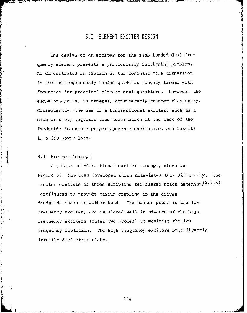
5.0 ELEMENT EXCITER DESIGN
Tne design of an exciter for the slab loaded dual fre-
cluency element presents a particularly intriguing problem.
As demonstrated in section 3, the dominant mode dispersion
in the inhomogeneously loaded guide is roughly linear with
frequency for practical element configurations. However, the
slope of t /k is, in general, considerably greater than unity.
Consequently, the use of a bidirectional exciter, such as a
stub or slot, requires load termination at the back of the
feedguide to ensure proper aperture excitation, and results
in a 3dB power loss.
5.1 Exciter Concept
A unique uni-directional exciter concept, shown in
Figure 62, hla been developed which alleviates this Iiffiiitv. The
exciter consists of three stripline fed flared notch antennas, ( 2 ' 3 ' 4 )
configured to provide maxium couplinq to the driven
feedguide modes in either band. The center probe is the low
frequency exciter, and is placed well in advance of the high
frequency exciters (outer two probes) to maximize the low
frequency isolation. The high frequency exciters butt directly
into the dielectric slabs.
134
HIGH-FREQUENCYFLARED NOTCH
PLAUNCHER
I
,, LOW-FREQUENCY
, . ""FLARED NOTCHI 1 LAUNCHER
VTOWARD APERTURE PLANE
Figure 62. Stripline Fed Notch Exciter for Twin Dielectric SlabLoaded Rectangular Waveguide Dual Frequency Array Element
L 135

L
The basic exciter is shown in Figure 63. It is formed
by symmetrically etching the outer conductor of symmetric
stripline board to form flared notches which terminate with
maximum aperture at the board edge and short circuit at the
notch bottom. The stripline center conductor is configured
to cross the notch regic~n at a right angle to the notch center
line, and terminates in an open circuit. By appropriately
selecting the distance x2 , from the center conductor center
line to the notch short circuit, and the distance Y2, from
the notch edge to the center conductor open circuit, the
exciter is matched in the feedguide environment over the
operating band.
A particularly attractive feature of the flared notch
exciter "s that the stripline board is plugged into the back
of the -lement. This considerably simplifies feed design.
In addition, the phase shifter and exciter may be integrated
into a single unit.
The exciter geometry shown in Figure 62 results in
natural isolation between the low and high frequency probes
in the low frequency band. Since the stripline outer
conductor is etched only near the board edge, the center probe
provides a short circuit bifurcation of the guide in the
L 136

METALIZATIONCONNECTOR
STRIPLINE FEED
AND COUPLING PROBE SEPTUM
Figure 63. Basic Notch Exciter
137
[,J
vicinity of the high frequency probes. Consequently, the
outer probes are in effectively below cut-off guide in the low
frequency band, and their excitation is governed by the
longitudinal separation between center probe notch bottom
and leading edges of the outer probes.
In the high frequency band, the outer probes couple into
the LSE 1 0 mode of the loaded half width guide and some natural
probe isolation is achieved due to the low field strength
along the outer conductors of the center probe. However,
the discontinuity at the center probe termination results
in scattering back into the low frequency port. This diffi-
culty may be removed by introducing an appropriately placed
shorting stub along the low frequency probe center conductor,
but the impact of this technique on high frequency aperture
field distributions has not been determined and remains a
design problem for future consideration.
5.2 Experimental Investigation of the Stripline Fed Flared
Notch Exciter
Experimental investigation of the stripline fed flared
notch exciter and exciter design were initiated during the
contract period. In general, the anticipated results were
obtained, and demonstrate the viability of the concept.
138
?,~
Notch exciter designs were developed to provide better than
2:1 VSWR looking into the load terminated feedguide over
greater than 10% band widths, and greater than 50dB probe
isolation in the low frequency band.
The baseline exciter design, a scaled version of a
previously designed antenna element, is shown in Figure 64.
The dielectric is Rexolite. The etched notch region has
uniform width of .058" for a length of .154" from the notch
short circuit, and then flares smoothly to a width of .400"
at the board edge. The centerline of the stripline center
conductor crosses the notch .135" from the short circuit.
In the vicinity of the notch, the stripline impedance is 80
ohms, and transistions smoothly to 50 ohms at the connector
junction. For the experimental investigation, only the
center conductor open circuit location, y2, was varied.
Five exciter elements, differing only in open circuit
location, were fabricated and tested using an HP Automatic
Network Analyzer (ANA). The values of y2 for these elements,
designated P1 through P5, are given in Table 5. In the 4GHZ
band, exciter P5 produced the best overall match. In the 8
GHZ band, P1 gave best results.
Measured VSWR for the P5 exciter is shown in Figure 65.
139
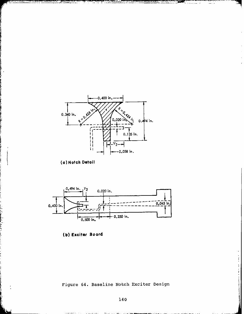
0.o400,in.--
0. 340 in. Nv
II.n0.020 n 0.494 in.
,! I J-,--0,058 in.
(a) Notch Detail
S0.494 in. y ,2 0 n _0.~~00.0- in.
0.0. in.
(b) Exciter Board
Figure 64. Baseline Notch Exciter Design
140
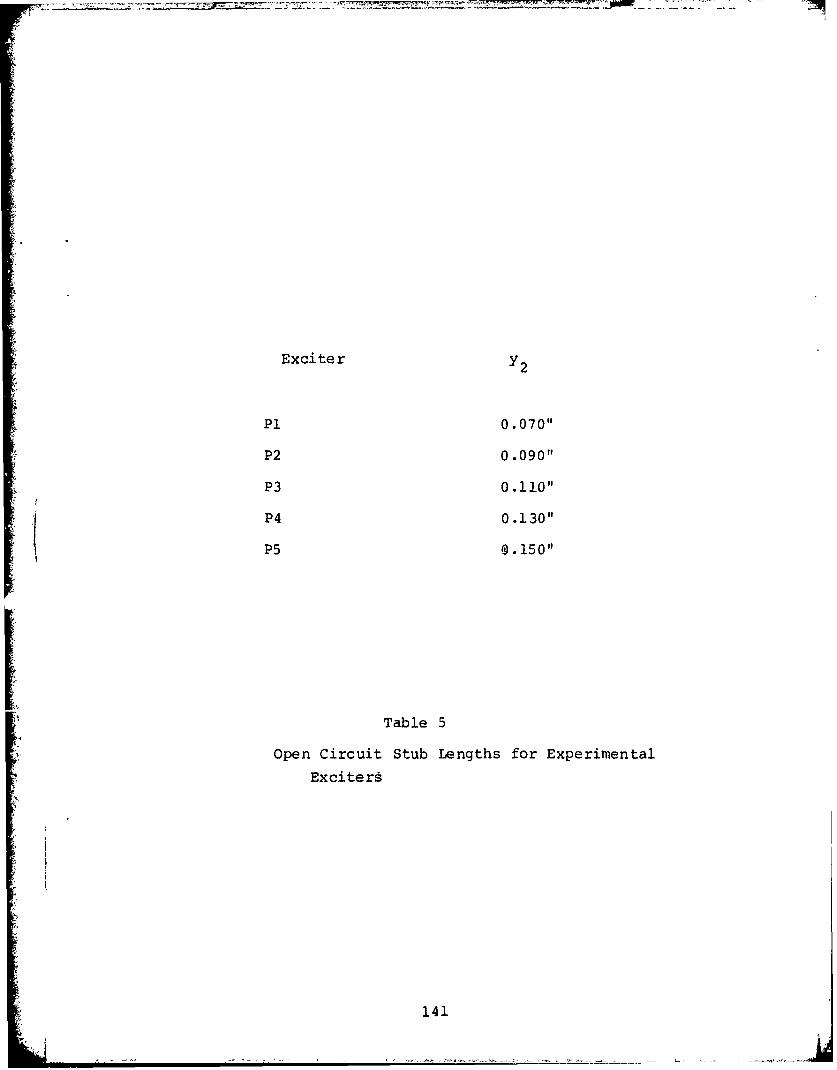
Exciter Y2
P1 0. 070"
P2 0.090"
P3 0.110"
P4 0.130"
P5 0 .150"
Table 5
Open Circuit Stub Lengths for Experimental
Excite rs
141

5.0
4.0-
3.0-
2.0 -
4.0 5.0 6.0FREQUENCY (GHz)
Figure 65. Measured VSWR for the P5 Exciter, 4 to 6 GHz
142
The measurement band is 4 to 6 GHZ. From 4 to 4.7GHZ, the
exciter is poorly matched, and is operating in the vicinity
of its low frequence cutoff.( 4) From 4.7 GHZ to 5.75 GHZ,
the mismatch is below 2:1. The low frequency cut-off
phenomenon is known to occur when the open and short circuit
stub lengths (x2 and Y2 in Figure 64) become electrically
short. Consequently, by increasing the notch depth and center
conductor stub length, the exciter operating band may be
readily reduced to the band of interest.
The ripple in the well-matched region of the experimental
band may also be largely eliminated by judicious selection
of the stub lengths. In the study of isolated notch antennas, (4)
it was found that similar ripple in reflection coefficient
occurred when the electrical lengths of the stubs were
significantly different. Since the spectrum of guided waves
in the region of the notch short circuit may be determined
in a straight forward manner, the proper stub length ratio
is obtainable by either analytical or experimental means.
Measured VSWR for the P1 exciter looking into load
terminated half width loaded guide is shown in Figure 66.
The measurement band is 7.5 to 8.5 GHZ. The match is below
2:1 throughout the band. It is evident from the figure that
143Ld

2.2000 - -- - - -
-0.1000
/DIV
HEAD CHANGE
VSWR--
MEAS I
1.20007500.0 100.00/DIV 8500.0
FREQUENCY (MHz)
Figure 66. Measured VSWR for the P1 Exciter, 7.5 to 8.5 GHz
144

the low end of the experimental band is quite close to the
low frequency cutoff for the exciter and that some stub
lengthening is required to extend the bandwidth to cover the
full 16% operating band. The discontinuity at 8 GHZ is due
to the automatic head change on the ANA. While the ripple
shown in the Figure is not large, some improvement can be
achieved by adjusting the stub length ratio.
Probe isolation is determined by exciting a single high
frequency probe in the three probe load terminated configuration
and measuring return power in the center probe. In the high
frequency band, the measured result corresponds, roughly, to
equal excitation of LSE1 0 and LSE 20 modes in the probe free
i jregion of the test device, and consequently is an improper
excitation for high frequency operation. Below the loaded
halfwidth guide cut-off frequency, the measurement approximates
the band isolation at broadside.
Measured isolation from 3.5 to 8.5 GHZ is shown in
Figure 67. The center probe is the P5 exciter and is inserted
into the guide 1.80" beyond the Pl exciters. The high
frequency exciters are butted against the dielectric slabs
and arranged such that the slab and exciter midplanes are
co~lanar. Below 5.8GHZ (the halfwidth loaded guide cutoff
frequency) the measured isolation is greater than 40dB, and
145

r_ _ -- -" - --
10 0 .0
D I I -IIIIII I Ii
ti E A I- - - -- -
i I
I I
I-I
II I t I. _ ! . .I.I " -- " - I -
3,500.0I I
I , IIIII II
FREQUENCY I I I
Figr 6 . r Me e P Is I I I 8
I I
I Ii
I I I
I I'rIS 1 I1'
. .. - r.. . .' ... .. L.-.. -I. . " . .I f lI I 2iIII " iL I IIII
;IIII- l, I I II
I2 II I'
III I II
IIII
Fiur 67 Mesue Probe Isoain 3. to85H
I I J i I ;146
exceeds 50dB from 3.5 to 5.0 GHZ. As anticipated, the
isolation in dB shows a roughly linear decrease from 5.5 to
5.8 GHZ. Above 5.8 GHZ, the isolation rapidly degenerates
to 12dB at 8.5 GHZ.
The weak isolation in the 7.5 to 8.5 GHZ band is due
to the LSEI0 mode constituant of the waveguide field in the
plane of the center probe board edge. As was shown in
section 3.2, the LSEz relative modal electric field strength
along the loaded guide centerline will be on the order of
.3 to .4 for a slab relative permittivity of 5. Consequently,
improved high frequency isolation can be obtained by either
tapering the center probe board thickness near the edge, or
by introducing an appropriately located shorting stub along
the low frequency probe center conductor. In general, the
first alternative seems best since it minimizes aperture
perturbations, but may be impractical. The second approach
has several difficulties associated with perturbations of
the field at the radiating aperture, but is readily implemented.
Clearly, the high frequency isolation presents a problem
which will only be resolved through further study.
147

6.0 CONCLUSIONS
The bifurcated twin dielectric slab loaded rectangular
wave guide has been shown to be a viable candidate as a
dual frequency array element which results in a considerable
reduction in electronic components relative to other multi-
frequency aperture techniques. In comparison with wide band
elements, the bifurcated twin dielectric slab loaded rectangular
waveguide element requires 21% fewer controls per unit aperture
area for equivalent scan and gain specifications.
To provide the multi-mode aperture control required for
dual frequency operation, a unidirectional stripline fed
notch exciter concept has been investigated which results in
greater than 50dB isolation between high and low frequency
probes in the low frequency operating band. Preliminary
exciter designs have been shown to remain well matched over
greater than 10% bandwidths.
An element design for operation over 16% frequency
bands cenLered at 4 and 8 GHZ has ben fabricated and tested
in waveguide simulators. Measured results are in excellent
agreement with theoretica- predictions in the 4.0 to 4.32
GHZ and 7.32 to 8.08 GHZ bands. Measured results outside
these bands were not obtained due to limitations of measurement
148

.~.. .. 7- 7. ... .
equipment (below 4 GHZ) and computational practicallity
(above 8.08 GHZ), but are expected to show similar close
agreement with theory in small array testing.
149

APPENDIX A
EVALUATION OF THE Epqr,nm FOR RECTAINGULAR LATTICE
The coefficients E are defined by the integralpqrnnm
i3+,1 A/2
(A-1) Eqrm dyf dx ep (xy) e*a (x,y)pr f-nm - pqr
b, -A/2
where A is the x dimension of the guide, B is the y dimen-
sion of the guide, b, is the half-thickness of the septum,
ep (x,y) is an LSM (p = ') or LSE (p = ") feedguideLS rim LS nm
electric mode function, and e (x,y) is a cell guide elec-pqrtric mode function which is an E mode with respect to the
array normal (r = 1) or an H mode (r = 2). By appropriate
choice of ordering in both feedguide and cell guide regimes,
single subscripts may be used to identify the modes. These
indices are taken as i for the feedguide mode modes, and a,
for the cell modes, giving
B+ij A/2
(A-2) E dy dy e.(xy)* e* (x,y)Ci J f - a
b1 -A/2
Expressions for ei(x,y) are given in chapter 3, and
expressions for e (x,y) are given in equation 8.--a0
150

In all, there are eight forms of the integral E
corresponding to the possible inner products of feedguide
and cell guide modes. These are:
1. LSM-Symmetric Modes with E-Modes
2. LSM-Symmetric Modes with H-Modes
3. LSM-Antisymmetric Modes with E-Modes
4. LSM-Antisymmetric Modes with H-Modes
5. LSE-Symmetric Modes with E-Modes
6. LSE-Symmetric Modes with H-Modes
7. LSE-Antisymmetric Modes with E-Modes
8. LSE-Antisymmetric Modes with H-Modes
t2Since the integrals possess many terms in common, these
terw3 are defined first and will be used as simple variables
to shorten the expressions. These terms are:
sin(kx+Ki)a
3 K - )
sin (kx -K i0)0R2 .ix _i
R4 = cos (k x- K E)
0Sikc xcfK
XG151
sin (k X G -KF)-R% =-
(kx-Ki)6
sin(k iR6 =
(kx - Ki )6
cos (k x- i )
P7k + K.
cos (k -Ki)
R 8 = k + K.x 1
sin (k xKi)
(kx- )c
sn (k K-)a
jk ybI jky i
and = e (l-e cos mR)
Im " 2
The coef icients 8'6, B"? , C', E, E'2 , F , 2
C", E , E' , F" , N! , N!A, N!' , and N!'A w hich appear
in the following expressions are defined in Appendix D.
1. LSM-Symmetric Modes with E-Modes
152
(A-3) E CTS /j1{kkj , k
where
MEi 2k 0( -) 11(R 1 +R2 + i- [3R - ]sink ~(A-) =B + r [+R, k2 K.XC
+ BI 81 R5+R6] cosk f3Y
I2K
+ B2 [ cI + 3 J 4r k
B2'~ [R6 -. R5]sink Bsr X
2k X
C 2 KA R 7-R 8 sink 2i
F+C' [Rg+R 1 0 ]lcosk -
and
K.= T k II [R
(A-5) -1 k R-R 1 1
+ .1 2K
2 2 2sn X(3kc K k2 -K..~
r ei XU) cj
153

KB+ - [R6 -R 5]coskxo3
K 2 2k Q+ cixc
2 - R3-R4 ]cosk2 2 k 2 K 2 X0r -i x c ' i
K B!+ [Rs+R 6 ]sinkxo3
E~ K 2 XGr i
K.C' 2K.+ k1 - + R7-R8]sink Ak' k 2 _K?2
2i K. C' x
+ I [Rio-Rgcosk AIk 2_K.- x 2
2. LSM Symmetric Modes with H-Modes.
(A-6) E0, i - {krki1- k II
where It and I are defined in equations (A-4) and (A-5),
respectively.
3. LSM-Antisymmetric Modes with E-Modes
154

whr
2k
-i {R-R + ElI XO R 3-R4 ]coskB C 2 2
+ L.1~ [R5+RGlsink$5r x a
2K+.E~ ( 2 + R3-R4]sink
k2 * 2 xo;
+LEl [R5-R6 ]coskr xc;
2kac A+F, [R7+R8 -2 l-cosk-
k 2 K 2 xay2
AL ~+ F'[R9+Rjosink j2
and
(A-9) 14 jk yK [R1 +1Z2]ycBk 2 -K?
K .EI 2
+ [ -+ R3 -iR4coskake-K 2 . k 2 -K2 . xc;
r Si I xcY cl
155J

K .E+ - - [R6-Rslsink xu
r Ei
K CE 2k+ i [R 3+ R 4 2 x ]s in k x 32k 2 - 2 xo2 -
k -K.r ci xa ci
+ ". 2 [Rs+R 6 ]coskxo32 2 Xr 6i
K.F' 2K.+ -1 (Re-R 7 - 1 cosk A
k 2_ .2 k 2 XC'2-
1 XG 1
K.F' A
+ 2 [RIo-Rg]sinkk 2 <.2
4. LSM-Antisymmetric Modes with H-Modes.
A-10) E {k I3 - k i'}
where I and I are defined in equations (A -8) and (A-9),
respective ly.
L156
F 5.LSIE-Symetraic Modues with E-Modes
S(A-li) U . = k I"Nil v-kto y
whe re
2K(A-12) V= j k y R2+R1 +B3' [; 2 + R3 -.Rdcoskx 3
0ci
+ B'2 [R6-Rb1sink
2k+ Bit [RI4-X sink ~
k 2-K. 2 xc
+ B'I' IRs+R 6 ]cosk xa3
C 2K. A
+ " Re-R 7- 21 2 Icosk-k. XJ
+ CV [R10-R9 ]sinkAxG2
157
6. LSE-Symmetric Modes with H-Modes
where Ig is defined in equation (A -12).
7. LSE-Antisymmetric Modes with E-Modes
~S
(A-14) E A y- ( )
where
2K(A-15) I= jk {R2-Rl+ E' [R4-R- £] ]sink
k -K .
+ E'2 [R 6-Rb]cosk xl
2kEll [R3+R 2 2cosk
K K
158
+ E'' [-R5 -R6]sink 0a
+ F' 2 + R7 -R 8 ]sinkx0 A
k - K .1X 0
+ F" [R 1 0-Rglcosk A
8. LSE-Antisymmetric Modes with H-Modes
(A-16) E S~ ! C-Itc (-jk It'6
where 1'6 is defined in equation (A -15)
Li ~ ~159 --

APPENDIX B
DERIVATION OF DIFFERENTIAL EQUATIOIN RELATING _ AND _
The homogeneous Maxwell field equations are
(B-l) V x E (x) = -jwpH(x)
(B-2 ) V x H (x) = jeE (x)
To separate out longitudinal components ( o directed) take
vector and scalar products of (B-1) and (B-2) with
Thus
(B-3) jwiH(x)x.o = z x(VxE(x)) = E(x) + VE (W-- 0 o - .- z
(-- - ( xE(X + e(x)) + (Vt+Z z)E (x)z -0 . . .. 3
= VtE (x) - (x)--z 3z (x
160
- -4%4f a-. - - . . - -
(B- 4 ) -j3 Hz = z . (VxE(x)) -V ' (ZoXE(x))
where e(x) is the tranverse to z electric field.
Similarly,
(B-5) jwZ o x E(x) = V tHz(X) -z h(x)^
(B-6) jwE z (x) = Vt (HxZ 0
Substituting for Ez(x) in (B-3) from (B-6) gives:
A V t A
(B- 7 ) - - (x) = jw[-I + -- ] (h(x) x Z )
Recognizing that
Ae(x) e-jyze(x,y)
A -jyzh(x) = e h(x,y)
for uniform (in zo) media, (B-7) reduces to
-o1
161

tvt(B-8) L- e(x,y) = [I + k (h(x,y) x zW-o
And from CB-4) and (B-5)
(B-9) yh(x,y) = r[ + t--1 ,ZXe(x,y))
For the inhomogeneously filled, uniform in zo wave-
guide,uncoupled modes will be either LSE (e" = ) or LSMx
(hx - 0). For LSE modes, solution of (B-8) gives
e y(X,y) = - h"(x,y)k 2 k2 xk X
e" is related to h" by an impedance. It is convenient,y x
therefore, to define a modal admittance Y", such that
e"(x,y) = -h"(x,y)
y x
and
fJdA(hi ) • = ..-, 1)
162

In this manner, (B-8) may be rewritten as
(B-1O) yZ" e"(x,y) = (.[I + - -] • (h"(x,y)xzo
Similarly
(B-Il) yY'h' (x,y) = h Ioc + (z- x e' (x,y))
163

APPENDIX C
ORTOH OR1ALIZATIOi OF FEEDGUIDE MODE FUiCTIONS
Let Ln11 and E ,1 be linearly ind-pendent character-
istic :oLutions of Maxwell's source free equations in the cyl.-
indrical guide shown in Figure D-1. The guide is uniform in
z, resulting in z dependencies given by
-jY nz e-jmZe , e
Assuming a lossless region, then the conjugates of the
characteristic solutions are also solutions of Maxwell's
Equations. Consider the curl equations
(c- la, b) VxE = -j If % xI.:m = j'
(C-ic,d) VxHn j, sE Vx}!* = -j, o:E*n -n -m i
where * denotes conjugation. Taking scalar products of
(C-la,b) with H* and 11, respect-ively, and addinq, qives
(C- 2 ) 11* VxE + I i xE* .0
--m -n --n "
Simi larly, from (c-lc,d)
164

(C-3) E* .Vx +E . VxH* 0
Adding (C-2) and (C-3) and manipulating results in
(C-4) 0 :V t (E*xHn + E xH*)t -in- -n --in
+ zo~* + E xH*)+ a z W n -n -m
where Vt is the transverse gradient operator, and the longi-
tudinal gradient has been specifically shown. Since the entire
z dependence is embodied in the exponentials, (C-4) becomes
(C-5) V t (E,*xH + EnXH )
j )Z (E* x H + E XH*)= (yn-m t -t t
m n n m
where the transverse field is indicated by the subscript t.
In equation (C-5) the longitudinal components of the fields
have been ignored on the right hand side due to the z0 .
operator. Let
-jy z(c-6) Et = en (x,y) e
n
and similarly for the other explicitly transverse field
quantities (subscript t). Then, application of the diverg-
ence theorem (z-dependent integrals cancel out) results in
165

(C-7) -Y x hn + e x h*)da : 0n- -n n
where S is the cylindrical cross-section and da is the
differential unit of transverse area.
The fields En, Hn, E, and H are assumed to be linearly
independent. Hence yn -m and (C- 7 ) may be rewritten as
(C-8) Jzo. (e* x h + e x h*)da 0-i -n -n -ins
Since the direction of propagation (±z) should not effect the
result (c-8), consider the z dependencies
-jY z +jY zn ine , e
Then, by entirely equivalent steps,
(C-9) (Y+y)ff . (e* x h - e x h*)da 0(9) (nm - -in -n -n --mS
or, for yn -ym'
(C-10) JJzo • ( xh -e x h)do= 0
Adding and subtracting (C-8) and (C-9) results in
166
L

(C-I1) ffe* . (h x z0 )da = 0
(c-12) Bie . (h* x z 0 )d =0
Equations (C-li) and (C-12) are the desired mode orthogonality
relations.
In the instance that y = ,m' then, assuming the eigen-
values are not degenerate, equation (C-7) is satisfied indepen-
dent of the value of the integral. From equation (C-10), with
m-n
(C-13) e* x h = e x h*-n -n -n -n
Substituting (C-13) into
(C-14) l Z0 . x h + e x h*)du = constantY ,-n -n -n
yields the desired mode function normalization integral
(C-15) fe . (h n x z 0 )da = constant
If the constant in equation (C-15) is taken ac 1, then
in the field representations
167
E= V.e.- i -1
H = I.h.
V I* has units of power.
Usi ng the expressions for er and hr (r=',") from section
4 in equation (C-15) with unit constant, and rearrancginq
results in the following integrals for the nurmalization,
constant N.:1
1. LSM symetric moles (r=')A/z b
Jd~W 7 I2rlt(X) K(jJ) =dyn (), :bi n-A/2 0 r
= {-S (2.' -) + 213 '. S (2.'+r
<,C'l, I ' t N
where
C co Svcos,<' ;
r r i 4' *
--- -s ink ',
s' r ... *lotosE-' ,% + -- cot, ' s5113,1
I IrK

and
11, x-IxI
I x=-jI XI
S1 () =SLIX= 1X
S2 Cx) = sifx +x
sin xS2(X) - tx
2. LSM antisymmetric modes (r=')A/2 b
(Na)' fd x Jdy~ (xsinl n
nm =-A/2 0 P r~x
b(S 2 (2K' ) + E 2'6r
+1 -JEJ I2"S (2K,'V (K,)r
r
wherc
El sinK'
E2 K COSK$
169

Ff COSK[COSK'1 S K - -tanK'asinK, ]
siKC E rK C
lm{EIEJ*}, K, = -jIK'IC
3. LSE symmetric modes (r=")A/2 b
(N"5) fdx fdyCOS2M7ZIV1 5S(X)12M -A/2 0b n
r rb{- S,(2K"- ) + Vt2f SSJ2KHf
C E E
+ Icoo I '2(2Ka) G(K"')
where
r =Neumann f actor
B2 K"It
Ml COSK" K",
C {COSK" ,,tarlK"$6sinK'61
170

4. LSE antisymmetric modes (r=-")A/2 b
(N11a JdX fdyCOS2M"Y1VI#a(X)I2nm -A/2 0 b n
+ I E 1211 2 SS(2(2K((Kl)
-F6S 3 (K"6)
ISF I2 (2K "a)}
where
El' -sifK"O3
=K
F _inK COSK" 6 ,-oK iK6
s~K in1K"It c
F=Ref{E',E"*}, K"= IK"I, K" IKI
-:0.5{ Elt-El*}E", K" 1 -jIK" I K" 1Kl
L171
APPENDIX D
PROGRAM LISTINGS
This Appendix gives listings of all programs, and
subprograms required to reproduce the numerical results
presented in this report. In general, the listings are self-
explanatory. The language is FORTRAN (extended) and the
programs are designed to run on CDC 6600, 6700 and CYBER 73
series computers.
The Appendix has two subsections. The first gives
listings of main programs. The second section gives listing
of subroutines and function subprograms required for execution
of the main proycirms.
L172

_________________ ~
D.1 Program Listings
III
II.
r
V
173
PROGRAM PLIPAT (INPUTOUTPUToTAPESuINPUT,1APE63UUTPuTTAPL4)
9c COMPUTATION OF~ BIFURCA TED T6IN rn!ELECTRIC SLAB LUADED RECTANGULAR~
C vAVEGUIDE ARRAY E.LEmErT RADIATION CH.ARACIEHISTICS,
C REUUIRE.S CALCOMP LIBRARY AND SU4ROUTINLS GIVEN IN APPENDIX D,29
DIMENSION PUW(lQ9b1),ST(N1)SlT(2)S2()MR)(2O)IP(0)IU1O)tIIRC 10) 9JJ( 10)DIME.NSIUN IbUF(UUO)RFAL A9KE9LINTEGER P19o'~1 TUC1O) ,(O(I0) ,RO(1O),SIGO(10) oSIG(2O),SIG1O(10)COMPLEX YYAd.1UC20,CI ,C2,AJC3,R1,R2,CL4COMPLEX S11(?0,2O)9S21(2sq0,~)#VOCOMMONv /ARRAY/ ALBLU)LB1,SEPTLTPIEPSS1(2)9S?(2)COMMON /CNSYV/ Y(2O)ofA(2SO)COMMON /MUDES/ K(2O) 0KE(2O),GAMMA(20),MODE1 (2U) ,ISYM(20) ,NN(20),1Mm(2O)#MOD~kD(20)COMMON /Pu/ P1,U1DATA TP1,C/b.283185307179b,11.8G28526/DATA AJ/(Uoo.I)/CALL PLOTS (IBUFt.100,L)KNT80
CC INFUT~o FRLQUENCY IN GHZt FO# RELATIVE SLAB PERMITTIVITY, EPSOC FEED(iUIDE HEIGHT, 8D9 IN INCHES* A(ALPHA)t B(BLTA), AND DCUELTA),C IN INCHES# AND APERTURE PLAN Tu-REPFkENCL PLANE SEPARATION IN
[C FEEDGUIDE 6AVELENGTHS9 ALEN,C100 READ (59800) F09EPSBD@A@89DSEF-,4LN
IF (EUF(5)oNE*0) G.O TO 160A1S29*(A+e*D)VYRITE (69'90U) F0,EPS9Al9HAL),6#UqSEP#ALEN
c INPUT> LIMITS OF SAMPLED CRATING LOB~E SPACE, PI AN 01
READ) (5#820) P1901C
C INPUT> LATTICE VECTORS Si AND b?, iN INCHES,
DO 105 48192
105 CONTINUE
IGRLI
IF (AbS(S),LT~1.L-1O) TGR~a?
DysS2(2)CC INPUT), NUMBER UP MOUFS To ESTARLISH ORDERIN,, NMODE1, *rvAX OFC 2000 AND FREQUENCY HAND DESIGNATION, LOHIO=LU3 OR HI0.C
READ (59810) 14MUU)E19LUH1IHLOXLDHIIF (SEP#GI.1.E-1OJ IHLO:22HLO
CC INPUT~o SINE SFACE SCAN~ kA .GE AND INCREMLNTS.C
174

(5AD,8t00) STHSSTHtSTHlSPHSSPIESPHINTI$BINTCCSTHEoSlNS)/STt41+0.5)*1NPHUZNTC (8PHEoSPH3)/SPHX4O,5)41
c INPUTb NUMBER OF FEEDGUIDE MODES 10 BE USED FOR APERTURE FIELD
C APPROXIMATION, NMODES* AND NUMBER OF BEAMS TO BE PLOTTED, LOBESs
READ (5,820) NMODLSLUSS
NMvNMODES+1Do 106 Ix1,NmODE3
V CC INPUlb NMODES FEEDGU!I)E MODE UESIGNATIONS *E#G., LSE0100#c LSMO1O19 LSEOW0t#
READ (5,830) MOROCI)106 CONTINUE
IF (LOBES*E~d.U) GO TO 108IF CLOBES.GT.10) STOP 'LOSEs&lO'
Cc INPUT' OLUSESO BEAM DESIGNATIONS IN FORM P#UIRC
Do 107 Is1oL0BESREAD (5,820) TO(I),u0(I)vH0CI)
1(2*0 lii)107 CONTINUECC INPUT3 COMPLEX LSE0200 MOD)E VULTAGE Muf F1Ewt RIO AND COMPLEX
C UPPER ELEMENT HALF VOLIAGE MODIFIER, R2,C108 READ) (5,800) R1,R2
WRIFE CbQOM) R1'N2WRIIE (69910) S1982WRITE (6991b) P1,W1,NMOUESLsF 0/CALMAOLBLBB*I.DLBU*L
SEPT LNSE P*LCC COMPUTE DISPERSIUN RELATION AT CENTER FJANUoC
CALL LSMLSE CNMUDEI)ALENUALEN/(L*GA1MA( 1))IF (ALENsGT.1.EuO5) ALENlEALENALENBALENICIOUCEXP(AJ*TPI*GAMMA( I *Al.FN*L)C2OUCEXP (AJ*TPI*GAMM A (2) *AIEN*L)
CC INFUT~o HALF RANDWIVIH (INTrEGER) 1N PENCLNI, IBbJ# AND) PENCENTC 9ANDvIDTH STEP9 ISTEF'.C
READ) (5,820) 1bw6918TEPN8W32*I BW4*i
CC COMPUTt PEkFUIRMANCE UVER PANL'.
Do s 1bJou1,NpotISTEF 7

FBSW*FO
IF (IBWsE(J.0) GO TO 108WRITE C6,905) 80iFftPSA1,BD9Ab9O,8EP9ALEN
109 LeFICAL@A*L806%#LDLBD*LBI.8D*LSeP TL*SEP*L
IF CIaw&E.oo) GO TO 1091CALL LSMLSE (NMODE1)
1091 CIBCIO*CEXP(UAJTYPI*GAMMA(1 )$ALEN*L)
C23C20*CEXP(-AJ*TPI*GAMmA (2)*AL&kN*L)
1 D0 C to 80
3. 0Do 116 In1,NmODLS
15 IF (MODORID(3)*NE9MORD(I)) Go YO 115
NSY(I)3sM(J)
MODORD(1)UMORD(I)116 CONTINUE
IWRITER1CALL NORM (NMOOLSIWRITE)SP8RSPHS*SPHID0 150 1PH81,NPHK NTUK N T 1Do 1164i 1.1,10Do 1163 ITHul,51
L POW(ItITH)3S1009001163 CONTINUE1164 CONTINUE
CPHUSORT(1..SPH**2) 6q)SP
IF (IHLO*EQ.2*4I) WRITE (69920) SPH
KJISOCC TAKE THETA CUTS*C
Do 140 ITHU1,NTH3TMUSTH4S1HIST CITH)BSTHCTMxuSRT (1 .STH$$2)
VmS TH* SPHC3sCEXP(AJ*TPI*V$bI 1L.. C~sR2/C3C33142*c3 176
CC EVALUATE SCATTERING bLUCI(S S11 AN~D S21
CALL. SCTMAT (IHLUNMOOE'StU#VStltS1,NMUDISIG)
K3UKJIDo III I111SIGIF (REAL(YA(I))eLL.0.) GO To 117IF (41.EQ.0) 9O To 1162Do 1161 TlI,19IF (IsEQ.oSIG(11)) GO TO 117
1161 CONTINUE.1162 JvJ+1
IF (3,LE*1O) GO TO 116S
31IiOCKJ)xI1165 SIGCJ~uI
17 CONTINUE3134J2u4IF C32*GT*10) 32210KJISKJIF CLOHI.EQo2MHH) GO TO 120Po2o*CAbS(Y(i))
C COMPUTE POWNER TRANSMISSION COEFFICIENTS FOR FIRST 10 PROPAGATINGC BEAMS IN GRATING LOBE SEQUENCE9 AT LUVW FHEQULNCY AND POWtRC REFLECTION COEFFICIENTS* PRINPUT FovER# PQU~tJm, OF REAL P~viER INC ALL BEAMS AND PEEDGUIDE MODES9
DO 118 I1q,4
PT.(CABSS321uISG.1)+21UISGNM),*a.*REAL(YA(ISG))/PSuREAL(YA(1SG))01.0IPTSIIF CABS(S) .LT.1.Eu1O.AND.ABS(SPH*CPH) .LT.1.E.-1O) IPTNIPT41IF (ABS(SPHu1.) .LT.1 .E'.O.AND.ISG.GT.ISIG/2) IPTUIPTm2IF (ABS(CP~sl.).LT.1 ,Em10.AND.ISG.LEISIG/2) IPTUIPTo2IPTXIA8SCIPT)PT81PT*PTPosP0tPTIF (PTe.L.10I) PT:1.E-1OIF CI*GT.1O) GO TO 118PoWdIITHJv1O.*ALUGI0 (PT)
Ila CONTINUEPRUn(CABS(S11 (1,1)+511(INM))**2,*CABS(C1)/PPospo+PRUIF (PRUeLT9.,eSIO) PRU21.EwjOPRU810o.ALOGIO(PRU)PRL5(CC~S(S11(NM,1)+S11(NMONM))**2)*CABS(Y(1))/PPO3POPRL
C CHECK CONSERVATION OF LE*RGYo TPO AND IM ARE MiINUS THE. NUMBER OPC DIGITS TO W~HICH CONSERVATION OF ENERGY IS APPROXIMATED BYC SOLUTION#C
PouALOG(AS(P01.o)e1 .EeSo)
IF CIPO*LT~o99) IPO:.99U

PRLx1O,*ALOG10(FRL) pL1EiCALL CONSRV (19P1NOSC9MWdRITE (9940) SIHPRUPRLTplTm,(PUW(!,T1H) 'Iu1'J2)GO 70 130
cC COMPUTE POWgER TRANSMLSION ANDL REFLE.CTIUN CUEFFICXENT$ AT t4IGC FREUENCY9C190 V2m1Ar4(0.25*TPI4S1(1)*(u)
VOSRI*V2VancAus(VO)PmCABS(Y (1) ) CAbS (V(2) )#2*IF (ItLUoNEoLOHI) Go in' 12'J
CC IP INFINITESSIMALLY THIN4 SEPTUM ANL' RECTANGULAR GRID@
00 121 Isl,4j1ISGSSIG(I)PTOREAL(YA(ISG))*(CABS(S21(ISGI)+S21(ISG,2)*VO)**2)/PSxREAL(YA(I3G))wl.OIPTal PIT1IF (A83(3).LT.1.ES10.ANUAS(SP.*CPH).LT.1.~W10) PxT+IF (ABB(SPHosI).LT.1.L.10.AND.!SG.GT.I$lG/2) iP7UIP7-2IF (ABS(CPH@1.).LT.1.EUIO.ANDPISGLE.ISIG/2) IPTxIPT-2
PTx1PT*PT
lit CONTINUE
PouPo+PRIIF (P141.LTo1.E-10) PRloEsIOPR1slo,*ALOGjo(P~j)
P08POIPR2CC CHLCK~ CONSERVATIUN OF LNERGY.
POZALOGlO (ABS (P0w1.0) l1sEw8o)
Ip (IPO*LTs-99) tPON-99IF (P1R2.LTq1.E'10) PR25l.E-IoPR2m10.$ALOL10(PR2)CALL CUNSRV (S1l9S21,NmUOTSTGIM)
Go TO 130CC CASE 2p THICK SEPTUte UP TpdANG1JLAN GRID*C,124 Pn2oo*P
P030.0DO 125 1919JIISGmSIG(I)PT3KEAL(YA(ISG))*(ABS((C21(ISG,1)$C4+821(lSGNM)*C3)*C1+1(S21CISGZ)*C4+1.21(ISC,,(vm+)*c)*C2*vo)**2)/PSuRLAL(YA(ISG))vI.0 178

IP~a1IF (AbS(S).LT.1.E.1Q.gAN~D.AiS(SP*CPH)LT.1.Ew1O) IPTBIPT91IF (ABS(5PM.1 .) LT.1.E.10.AND.ISG.G1.ISIG/2) IPTUIPTo2IF (AtiS(CPH.1 .).LTeld..l0.AND.1SG.LE.ISIG/2) IPTxIPTw2IP1UIASS(IPT)PTSIPT*PTPosPO+PTIF (PT*LTl.E-IQ) PlasI0IF (I*GT*1O) GO TU IRS
POW(I9ITH)31O.*ALOGIO (PT)125 CONTINUE
I+Sl1 (1,Nm+l )$C3)*C2*VO)**2),PPRU3-PHU.CABS(Y(2)4((S11 (2,t)*C4S11(2,NMo*C3)Cl+(S1I(2,2)*C4
[98 11(2,Nm4.1)*C3)*C2*VO)4*),PPouPO+PRULIF (PIRUeLT91*E.10) pRUv1.k*10PRU$I0**ALOGI 0(FRU)PRLXCAB8(Y(1)4((811(NM,1)*C4+S11(NMNm)*C3)C*(11(NM92)*C41*311 (NMNM+1)*C3)*C2*VO)**2)/PPRLUPRL4CABS(Y(2)*( (SiI (NM+ 1, I)*C'iS1 1 (NM+1 ,NM)$C3)*C1+
1(81 1(NM*1,2)*C49S11 (NM+1,NM,1 ,*C3)*C2*vO)**2)/P
CC CHE.CK CONSE.RVATION OF ENERGY,
POWALOG1O(A63(Pm0wq)*I .E.-o)IPouPoIF (IPOLT*o99) IPmou99IF~ (PRLvLTo1.Ew10) PRLs1.EwIOPRLX1O**ALOGIO(PRL)CALL CON3fRV CSII,523.,NMUDIsIG9IM)NrdRE (6,940) STN.PRUPfRLIP0,IM,(PUW(IITH),I319j2)
130 CONTINUE140 CONTINUECC PRINT BEAM DESIi4ATIUN'S,
ISGOISIG/2Do :41 Ix1o42DO 1410 Ilxls'OdESIF (SIG(I)sNF.SIGQ(jI)) GO TO 1410
GO TO 14111410 CONTINU.1411 IR(I)BI
IF (8jG(I)sGT.I$G) IRUI)s2
141 CONTINUEWRITE (bt95o P)10)IU)I14IF (KjloEU*U) GO TO 143DO 142 I1,PJ1IR(1)21IF (SIGlo(I)sGTvI3G) IR(I)82
14a CONTINUE - -
WRITE (6,960) (PI 1().RI ~1KI179

143 IF (LOBLSsEGS0) GO 70 150IF (KNTsEQ.1) CALL PLOT COo,.59-3)
CC PLOT #LOBES$ BEAMS
CALL PLOT (0,.o22)ISTRTalLOBEBMINO ('SLOBES)CALL PLICAL (A.8,DtFEPSA1 ,BoOXDYSEPPOW.SIGOLOBEISTRT.JJ,ISTSPH9IGRD9NTH)IF~ (LORESeLE.4) GO TO 150CALL PLOT (0922LOBLNMINO (49LOBLS.14)ISTRTw5CALL PLTCAL (A.8,OFEPSA1,BDI)XOYSEPPOWv,8IG0,LO8EISTRTJJ,I3TSPtlIGRDNT4)IF CLOBES.LE.8) GO TO 150CALL PLOT (0v22LoBE8MINO (2#LOBe.Sw8)I11T*9CALL PLTCAL (ABtOtF.EPSA1 ,BDDXOYSEPPOviSIG0,LOBEISTRTJJ,1ST9SPH91GRD#NTM)
150 CON71NUE155 CONTINUE
Go rO 100160 CALL PLOT (sos?*Z2)
CALL PLOT (10*90o.999)ENDFILE 14CALL EXIT
C800 FORMAT (8F10.0)610 FORMAT (I59QZ)820 FORMAT (1615)830 FORMAT WA)900 FORMAT (1l1,Le6X937HDUJAL FREQUENLY AR4RAY ELEMENT PATTERJS,,///,
1SX,13MELEMENT DATA&,/910X,5HFO 9 F5,295xthmEPS a ,F5.2,5X94HA 92F5#3t5Xts4H8 a ,P5o39/,qIX8H~ALPHA Z #F5,3,5X97HRETA a *FS.39SX938HDELTA a ,F5.3,5Xv9HSEPTUM a ,FS.,3,SX,1LJMALEW/LAV-8DA a F5.3,/)
9014 FORMAT (5X,18HVOLTAGE mOfnIFTERS&,,,10X95HRI 2 *2F7.49IHJobXtISHR2 a ,aFT.14,1HJ9/)
905 FORMAT (1H1,IOX,7HCASLL qF4.2f2HFO9//91OXSHF a ,F5*2,5Xv16HEPS 9 ,FS,2,SX94HA 2 9Fbs2v5X,48 2,F5*3t/,1OXSHALPHA &92FS*3tSX#7HB8VA a tF5*3t5X,8HDELTA 2 ,F5,3,5X99HSEPTUM 3 F~~3SX,7MALEN a 9F5.3,/)
910 FORMAT (SX911HAkRAY DATA&,/q1QX,94MSl ztP6s39lHvqF5s395X9siHS2 Z,1F6.39IH,,F5s3)
915 FORMAT (IOX94HPI Z#13#5x94Hr~1 U,1395X,8HNPOUES StI30/91Oxv12S4HALL DIMENSIONS IN INCHES,/)
920 FORMAT (lI1,X911HSIN(PHI) x ,FS.2,///,1X,7MSIN(TM),5X,3HPRU,5X,13HPRL,7X,3H1P0,2Xt2HIM,3X,3lHPOWER IN EXCITEU BEAMS (04) --&t//)
930 FORMAT (IHI,5XIIHSIN(P4I) s ,F5.20///,1Xo7HSlN(TM),5X,3H~FR15X,13MPN2,7x,3HIP0,aX,2MMXS1PUV.EH IN EXCITED SEAN'S (1)8) m,)
940 FORMAT (2XF5,2,9X2zdxxFb.~,Xt3X#2ad13,1X ,1o(1XF6.2.1X))950 FORMAT (/tSXt8MPfQR 3 ,26XqIO(1XI2*1HttI29lM,,I1))960 FORMAT (//,5XtZbHSPACE MODES NOT PRINTED ARt&,/q5XoHPq(1J. U
110(2(12,IM,)9i1,3X))END
3180

PROGRAM DE.SMOD (INPUTOUTPUTTAPF58INPUT,1APEb300TPUTTAPE7)
C COMPUTATION OF FIRST FOUR ROUTS OF SYMMETRIC AND ANTI-SYMMETRICC LSE AND LSM MODE DISPERSION RELATIONS twIlH M&O FOR TNIN DIELECTRICC SLA LOADED RECTANGULAR NAVEGUIDE IN RANGE I*LEK*A/2*ANDsC K*A/2*LE,4*
C CREATE$ DATA FILE INPUT FOR PROGRAM DESGN*C
DIMENSION B8(16JvG(j6)REAL K(16)vKA2COMMON /WAVGD/ A~btDvBITPIvFPSDATA CP1,TPI/3.7569b6b7.6,28518S3O8/
CC INPUT), A(ALPHA)t B(BE7A), AND n(DELIA)t IN INcJIES# GUIDE HEIGHT,C 81, IN INCHES* AND RELATIVE SLAS PERMITTIVITY9 EPS.C100 READ (5,800) A98909819EPS
IF (EOF(S)qNE,0) CALL EXITAAX2**(A+B+D)WRITE (6#910)WRITE (69900) A9BDB19EPSWRITE (7,900) A,88,19EPSEPSI83QRT(EPSw1.0)Do 110 131#168(I)vwEPSQ+1.Eel0
110 CONTINUEKA28*97Do 130 I19101KA28KA2+0@03FaCPI*KA2/AACALL FOURMD8 (F988)Do 120 Jul.18K(J)8KA2#BB(J)TvKA2**2.IK(j)*A8S(K(J))G(J)BSGRT(ABS(T))IF (T*LT909) GCJ)SOG(J)
IF (BB(J)#LT..EPSQ) 8B(J)xwEPSQI1.Ew10190 CONTINUE
WRITE (79900) KA2WRITE (69900) KA2WRITE (7.900) (tK(J),Js1,16)WRITE (69900) (G(4),Jx1.16)
130 CONTINUE
C Go TO 100800 FORMAT (BF10.0)900 FORMAT (0F10,6)910 FORMAT (181)
END
1814

PROGRAM DESGN (INPUTOLJ1PujTTAPE5,1NPUTTAPL6:UUTPLITTAPE1O)
C COMPUTATION OF BROAD)SIDE SCAN ELEML.NT 1-18MATLH FUR IIYFIN1T(C ARRAY OF BIFUR ATED ThIN DyFECTRIL SLAB LUALJFD IkECTA,tLILAoC wAVEGUIDES VS. K*A/2. USE rIN CONJUNCTi~oe4 V1TH PRUGRAMI DLSrOLJC WHICH CREATES TAPE10o
DIMENSION NM(10).NE(10),TI (l6),I(bM),IMODE(2),P1(2),PTlb(201O1)91PRl(2),PR1O8CZ)9SS1C2),SS2(2)REAL KKEKAC1OI)9m2BINTEGER P1,U1,8VM(2)
COMPLEX YYAS11(2O,20)9S21 (250tpo)COMMON /ARRAY/ ALBLUL,81LfSE.P1LiTPIEPS,81 (2) ,5(2)COMMON /CNSRV/ Y(20)tYA(25O)COMMON~ /MOflES/ K(UqE2~GM(utUt(0*SM2)6N2)1MM(20)vMODORD(2u)COMMON /PUa/ PI9U1DATA TPI/b.2831853071796/DATA IMODESYM/3HLSm9j1'LSEIHA,1HS/IWRITEsO
CC INPUT> SEPTUM THICKNESS, SEPT, IN INCHES* AND LATTICE VECTORbC 881 ANI) 552 IN INCHES,C
READ (59800) SEPTvSSl,5S2cC INPUT), NUMBER OF MOUES fOR APLR71JRF FIELD APPROXTMAIIU14 ANDC LIMITS OF SAMPLED 6RATING LOEk SPACE, P1 ANt) OleC
READ (59810) NMUUESP1,(jlMLO81IF (SEPToLTe1.E.10) MLOx2NOUNMOOES+1NMODEnNMODES
100 READ (10,800) Ao89D,~1,EPSIF (EUF(10)qNE$Q) GO TO 190AA229*CA+B4O)WRITE (69900) AABI ,A,~,DSEPTEPSNMUDES,8S1 ,SS?,PI ,W1AP829/(AA*TPI)WR17E (6,9940)Do 180 IFu1,l0lREAD) (10,800) KACIF)APISKA(IF)*APALsA*APIBLtsd*AP IDLNU*APIB1L881*APIM282(0.b/81L)#*2SEPT Lw SEPT *AP 1
8i(2)aAPI*SS1 (1)51 (Z)AP1*SS1 (2)
S2(2)*API*SS2(2)
READ (10,800) (Tl(I)oIuIt16)1080Do 12o inifibTIC I)%T1( 1)/KAC IF)
MOU(I.),M91182

Do Ito Jult"10810+1
Szl ..M~t*M**2mTl (I)*AH&S(T1(t))GsSWRT(AB8(S))IF (8,LT,0,) G3mGT1I0)xG
120 CONTINUEJal
130 Xul.,E+25DO 140 1u1,b4IF (XoGT*T(1)) GO To1~0
IBAI+(IA1)/16)/1'
XmT(IJ140 CONTINUL
GAMMA(J)XXT(IL')ao*E j+30TE84*(IA*.)18I
GxEPSm1.+K(J)*AtbS(K(J))SxSURT(ABS(G))IF (G9L7*0*) SMOSKE(J)2SMODO.31A/3+1moDL1 (J)xIMO0E(MUUE)MODExMOD (IA92+!SYm(J)USYm(mOUk.)NmCIC)2NM(IC) 4 1IA/3NE(lCI)*4IIC)(A/)NE C
ICInIC.IA/3NN(J)MN2
IF (IA.NE,3*OR.ICIeNh.0) GO TU 13oFNCUDE (10,9109N'OUORD(J)) .r)El (j)qN'2vIdl
IF (J,LENMUDES) GO 70 130CALL NORM (NMODL.SIWRITE)U200v20,
Dlo 170 IL02ML0,MLULUH132HLOIF (ILO.EW,2) LUM122HHI
IF (ILO*E(0.Z) SI(2):o.*,431?
CALL SCIMATIF (ILO*EQ*2) GU TU 150PT(IL0)3CA8S(S21UISG,1)4S21(ISG,!Qt)J**d
IF (PT(ILO)*Ll.1.L-1O)) PT( TL0)z1*E-10PTDb(ILUIF)210*sALOGIO(P1IL.)
IF (Pki (ILO) *LT*I*Ealo)PI LO:.t1PR108(IL0)X1O.*ALGOI.PNI(It 0))I, 183
PRzveU8=Ue*ALOGl0(PR2)GO 10 lb()
150 PTCILO)rnREAL(YA(ISG)/YUI))*CAdS(S21 (ISG,1))**2PT(ILO)z2q*A9S(PT(IL0))IF (PT(lLO) ,LTs1lstwO) .PT(ILO)*l*Ewl0PT~d(ILU,1)lv.YAL0GIOu(ITiLU))
IF (Pkl(ILO)).LTvl.E11.) PRlILO)slsL-10PRIlUB(ILO)810.*ALOGO(P41(110))
b CALL CONSRV CSllS21vI'PDOOIsGvIm)IF (ILU*E(*d) WMITE (b9950) KA(IF),LOHIP1(iLU)PTli(ILUIF),
IF (ILOeFQ*2) WR~ITE (o#960) KA(IF),LOH'IP(ILU)PTDa(ILUIF),IPRIOB(ILO)tIm
170 CONTINUL160 CONTINUE
Go TO 100190 CALL LXITC800 FORMAT (SF10.O)810 FORIAAT (105~)900 FORMAT (IHI, 4XIJ2HLUAL FREQjUENLY ARRAY ELEN'ENT DESIGN CtJRVES#
1///,1UXv13HELENlENT DATAP,,/q15X3H~A mFbq39bXt3Hl3 mFb.3,5X,27HALPH'A zFo.3,bx,6HBLTA x9F6,3v5X' 7I4ELTA Xtkb.395X#38HSEPTUM XF6,3,/,41SX5XHEPS x952b92b MnDE,//. lOX 1 1HARRAY DATA9,/9
b5X94HUIl 2,130/1X94HALL flI.,VETSIONS IN INCHES)910 FORmAT (A3ti?.e)9. Q FORMAT (2XA7o3X9Ab,2Xo3F1O.5qi4)940 FORMAT (IH1,L~bX,3bH4PEK TRANSMISSIUN FACION AT BROADSIDEO/O
159Xt12HVERSIS K*A/2,////9lOH MK*A/ce ,10MEXCITATION10H. PT
3b 30ox I 10H TYPE /9 FORmAT L3xF5a~tbXA2,4xL4(?X.F.3,lx),I7)90 FORMAT (3XF5.2,b~,A2,4X,3(2X.F7.3.1X) ,10A,17)
184-

D.2 Subroutine and Function Subprogram Listings
185

k SUBROuTIN. LSMLSL (NmufL.S)CC COMPUTE CHARACTENISTIC1,1 U 4~ n TSPELPST~l, K'LAT]', F.*m bY, ~T T LC INHOMOGENEUU)SLY LnA01r') RIECTAL,31,tL4A GO IUF.CC DEFINITIONS&LC B* GuiDLF ,IAPROV I'ES fl IvlEI, t~y
C FR.EL SPACL v.AVFLFi(;lH-rC EPS - RfELATjVt ITELEC1RIC C11',1TA'1T ,
C AL a DISTAVCE PRUm G~l -jAIL TO l~jEAlqSTCFDGt (IF LIjAI'Ii .G St, I~h iLt~,1
C EIL n - nI1 A \CL [RUM SL A, OGE( To bYrA'ELTr<YC~~~ PL A4 G~ VFF.I H S
C OL SLAHi THIC'k",LSS 0-JAVLL .tJG(T-is~C SEPTL * SEPIIW- U4ICO.LS5 I.11W RESPECT To, PREF,C SPALF A'AVELENGTHC TPI 6C FI a FPST LiATTICE %,tCT(,w
CS2 * P( LAI T IC E v E cIC K Xafl197FCTEL vAvEL-E' T :t AIlk ,I~o
C r,uJIL.F kITH kkbPLC I 10 FRFI: SPP~Ct
C -E X-P IPE ClFu v AVE".EU'H If': ()1FL E . I -ILC PFI~lr, LiF GuI.)E IjTti kESPECI T(. Fk~C sf-Ar F hvf .u% E.)
C FPi'LL 5PA(r4E ()RrMHwt aaa O~E~ yC I -C-Al, C'JI-UFP F RLE(JENXY
c MUE I1U21 T YPF 1L.9.1 LSE OR tS")cI SYM IA Y- F1 (I. S rP A)
INE 11y) ~Av, FREA 10PKAPE),MlpTA~BKG '0.E.,PTATI.NCOMNCARY ALLL, ,Sr P kL,T AYHS (NPLS) . CuS-OF
DIESIONP.
REAL( KA#KPqM8KBLK).COMN/RA/C9LUttEI#PgPtle922
IF ((0)MOO 2..QMD) 3
MlIU3MLMIBTIlODIsTPMODE.T? MUHEP (MDL.T.) M31118

M38MULA/3
KAPxsEPbQ41 ,Eo10
M3MOMM3Do 160 N81911Jul/N
IF (KAP#LT*Oe) suo0q99KAPSJ*KAPt( 1.j)*S4'KAP
KAPsKAPOKINC180
1010 KAPUKAP+KINCDIFFBOIFFI181+1KAPtE~PSl.KAP*AdS(KAP)SuSOHI (ABS(,KAPE))IF (A7P*,Ig~'gJ Sx,
K APE 88OIF1UD1P(OOUE9KAPXPLAlo1l'1,tEPS)IF (IsEQI.) GO TO 120IF (KINCLTIEEIU) Gu TO 130IF (AdS(0IFF*(D1PFl),LE.IE-l0) GO TU 130
110 KAP5,(AP-KINCKINC20958SKINC01FF l;OIFFGo 10 1on
120 DIFFSUIFFI4 GO TO 100130 IF (AtbSCDIFf).Ll.A8S(LiIPF1)) GO TO 14~0
Go TO 150140 KAPBKAPOKINC
KAPLSEPS1 +KAP$AOS(KAP)8SSWRT(Ai9S(AAPE))IF (KAPE,LT.O.) suwsK APER
150 S0(MODfENM0)8KAPSE(mOuE9N#MQ).xKAPEGui .um2B8*AHS(PKAP)*XAPSsSURT (ASCG))IF (G*LTs0,) 3m-SGAM(MUD~ ,NMUSS
160 CONTINUk180 CONTINUECC INCLUD. Y (I.Eso M) DEPENnENCEC
D0 183 mODEmI,4M 33 NODE/ 3
Do 182 "431,10KAPXSO (MODEvN, I)KAPESSE(MUOEtN, 1)Do 181 MOu29maSO CM0OE, N#,MO ) AP
SE CMOVENMU)*KAPEMs(MOoM3)**2BML3M2~9*m
L GZUKAP*AdSCKAP)41.OwbML17

IF (G2#LT, O.) GAIa 'ODE (\I ,:rA)s.C, Am( AUrm,#Nq.0)
112 CON IINUL183 CONrINUt
n 185 1xioll
NW, ( I ) zo
is CONJ1 lout
190 GAN-A (II:-1E 3(j
IF (~flntGT,2) P1 Z3HLSE
IF (&!UDEGT.2) m2:tl
Do 31 NC) u o /
IF (GAMMA (I ) G7 GA'-(MLIrGE ,o) r T n 200
GIAm ( I ) 2G OU o
ICM(
22 ON(..4E'
IF (IA9169,2)zt-F(L):Ej C)l ,
N(IzxM(I)~vC
IFDL (~ot'.1)
IF (IAGT2)2-. I ) SfI:it
MODI I (ed) ~ uFI )Ifffp( ),A"m1( I
~+iIF (I LE,-',j&'r)S) To 19.SEC 3SECUjL.(~WJRITE (Cb9930) $LC
900 FORMAT CI~iU910 FORMAT (AI.AI,21?a2) 188

9,20 FORMAT ('5XA8,'5AA7,5A.*F 1O,,C)X TS.)930 FoRMAI (SxtF20,39 8H bFC~l'f'))9'40 FORMAT (A9122
ENJD
189

FUNCTION DISPCMKKEABDER)CC COMPUTE DISPER31ON RELATION D(K99E) FOR ARbITRARY K AND KE
C DEF!NITIONW'
C M 0 MODE FUNCTION DESIGNATION a SEE CODEC K 0 X-DIRECTED VYAVENUMBER IN AIR REGIONC peRT KoC KE 0 XwDIRECTED WAVENUMBER IN DIELLCTRICC REGION vhRT KOC A a ALPHA/LAMUDOC s BETA/LAIm8DAOC D * nELTA/LAmODAO
C ER * RELATIVL PERMITTIV17Y OF SLABSCL
REA6 KtKE3A83INC(K*A)CABCO$C (K*A)S88SINC (K*B)Ct~3COSC(K*8)SDSSINCCKE*D)COUCOSC(XE*D)SKAn3XOX(K*A)*A
SKENSXOX (KE*D) *tS3231GN(1.tK)S223IGN(1.,KE)Go TO C1009110;1209130)9 m
CC LSM SYMMTeSMRIC MODESC
V RETURNCC LSE SYTMMET IRIC MODESC110 DISPgRKA* K*CSD*CB4K$SB*SKE*CO),CA*(K*S*S *SKBE.C*C)CB
RETURNCC L3E A~SYMMETRIC MODESC130 D13PUSKA*(C~iKE*S*BKB3*S*?)CA*(*OSb*C1SKPS)
RETURNEND
190

SUBHOuTL!NE 14ORM (NIAODJESIKRITE)CC SUbROL'IINE NUJRM COMPUTES THE FtFf GUIL)E :40kE INOMAL,1ZATIflb$ ANLDC VALUES FOR THE COEFFIrIFNTS APf'FARIl~j( liv THE FXPkESSIONS L)R VHI.AC AND IHAT OFOR vvH1CH SEt D0CLWpFhTATLONs,CC NOIE& THE COEIFJICIE14TS b~pPE,2kFPB0I',PE~*LvPE2(Dp miAy IbE
C REAL ON IMAGJNARV #N~OT Cumpt-Exo, ALL OTHER COEFFIIE~NTS AREACbWA'l8 REAL, ALSO, NORMALIZATIONS CARRY AN AO)DI10jNAL 1/L.Ami3)A 3C DEPENDENCE vdlICH CANLFLS IrN SCATI~kTNG MATRIX COMvPuTATOnmS, HUI
C NOT IN MUOE FUNCIT0ON CUmPUTATUJONS,5 C
CC EFIN!TILNS), SEE SIPUTNFLSMLSE
CC SUFFIXES-C p PRIN'E (LSPI MODWSC UP 00IJbLE PRIME (LSE 11O[)LS)C 8 SYM.N.FRICC A - ANTImSYMMLTRIL
REAL KAPAAPEK KLNP5,NPA t.inSNDPACOMmON /ARRAY/ ALRLD)LR1LSEPTI,,TFTEpS,5bl(2,,sS2(2)COMMON /COEFS/ d1P(10),a2P(IO) .8DP(1Q),gD(10),CP(1O) ,CuP(10),
2NnPS(lUhNDA(jQ) ,OtJNT(2O)COMMON /MODE$/ KAP(20),KAPEc20),GAN1(?O),MuDLI(20),tsyM1(20),
AxTPI*ALBoTPI*BLDxTPI*0L
IL.SE uO
DO 1'40 I11NMODLSK*KAP(I)KEXKAJE(T,)AKBK*A
DKEBD*KEMODESMODE 1(1)ISYMaISYMI (1)
IF (mODE.EQ.3HLSE) GO TO It0
C LSM MODESC
IF (l8YPMEQeIHA) GO TO 100CC SYMMETRICC
ILSMSS!LSMS91KOU~T (I );ILSMSS1P(ILSMS)BCOSC(BK)BP(ILSMS)mEPSSI$SINC(BK)/KF
82P(ILSMS)UB2P(lLSMS)*SlGNC1.,K)*SIGN(1.,tE)
CPCILSM3)sCP(ILSMS)/SINC(AK,
191

IDKE)*SI(N(.KE)*h2P(ILSMS);**)/FPS
3+AL*51 (2.,*AK)*CP(lLt Si)4*)NP$(ILSMS)XSQRT(AbS(Ai4OkM))GO 10 130
CC ANTI!SYMmETRIC
100 ILSMA.IL8MA*1KOUNT(T)IL8MA
EjP(ILSMA)uSThIC(HM) -
E2P(ILSMA)'.EP3*K*C0SC(bK)/ FFPUILSMA'mCUSC(BK)*(CU)SC(DKE).KE*1A( T(8K*SIII.(I,Ki*S1C;,C,K)
FzflP(h.SfrA)*EtfJ(lLSNlA)AN0RMXO.5*81L*bL*S(e.*K)OL*.S1 ?*DK) 1P(ILS'.'A)**2t
JAL*51(2**AK)*FP(ILS A)**?)NPA(ILSmA)xjRT(AS(AjnH'k'))BLUbL*SlGN( 1. KJGO 10 130
CC LSE MODES
110 Rmaso~IF (M.EQU) Rms~suIF (ISVm.EO~lMA) G;O TO 120
C SYMMETRIL
ILSLSnILSES+IKOUNT(I)mILSES
* 8tDP(ILSE8)zCUSC(8K)
1*SIQN( I * K)/3INC (AK)ANOHMuO.5iRM*RIL*(EBL*S1 (2.*EBK) +L*(S1 2.*DKL)*HlrU(LSFS)**2+ISIGN(1.,X)*(S2(2.*OD)*BflP(1L$ES)*2-2.4b1OP(LS S)*28D(LE .3,E)+A*22*K)b6(#K)*CpP(TLSES)**2JNDP$(IL3ES51(AFRS(AflURM))Go TO 130
C
120 ILSEAsILSEA+lALBAL*SIGN(1 * K)8L88L*SIGN(j@9K)KOUNTCI)2ILSEAElDP(ILSEA)8-SI14C(bK)E2DP(IL5FA)*K*CUSC (bK)/KEF DP (I L SLA ) a a81NC (b*K(C 0S CDK E+K 1 N CK t)/kM T A NT 8 K 5b4 C(A A
FsElDP(lL8EA)*Ed0P(lLSEA)ANORMsO.5*RM*BIL*(8L*SP(2.*RK)+UI *(SI (e'_*D$4j*FIDP(ILSEA)#*2+
2AL*32(2q*AK)*FDP(lLSEA)**2)
NDPA(lLSEA):SLURl(As(SNtURm)iALBAL*SIGN( I * K)19
BL3IdL*SlGN(lsvK
130 IF (IvvRITt.E0.O) Gf) TLI 11U
140 CONTINUE
RETURtN
900 FORMAT (1H1,5tH I liuH 914 E 910H GANI
-910 FORMAT (1x,13,Ix,3FlOsS92XA7,1XF1O.5)END
Li 193

SUBROUTINE. SCTMAT CLOHINNPOEStUoVOS11,SZ1,NMODSIG1)CC SCIMAT COMPUTE$ 1HE FFEflGUIDE a FREE SPACE SCATTERING MATRIXC oLUCKS Sit AND 321 FUR AN INFINITE RECTANGULAR GRID ARRAY OFc TWJIN DIELCTRIC SLAB LOADED RECTANGULAR W~AVEGUIDES*C LATTICE vECTURS at ANn S2
C LOMfI SPECIfIES WHlICH1 FREQUE)NCY RAND VLOHIZ2HL0 FOR LOWN FREQ~UENCY
C ~NOTEL IF TH SEPTUM THICKX.ESS IS NflI EQUJAL TO THE AALL THICKNESS
C~~3A~ LO~2LMtzAND TOR HIGH AN LROFU ~C FRQUNCYUNT ELS R
OFIEN ICAL,;UZLFN RAGL RGI O HC
C
C NMUE UMBER OF FEELGUIDE mOnES USED TO-'C APPROXIMATE APERTURE FIELD
C uo a I*H7)*rSPIC vo 0 SIN(THETA)*SIN(PHI)C S11 a FEEcDGUIDF SLF kEPLECTION SCATTLRIN(jC MLOCKC 521 a FEE4OGUILE TU SPACE MOUE~ VOLTA(IEC TWANSWTSSION COLFPICIENTC NMUD a NUMBFR OF FEEDGUIUF MODES IN UNIT CELL
jC SIGI * NUMtFR OF' SPACE MODES a 2*P1*UlC v F EfoguIlUE MODE ADMITTANCEC YA * SPACE MODE ADMITTANCEC #* OR OITHER DEFIf,,TTIUNS SEE SUb LSMLSE *CC SUPFIXES)- Ski SURxUuTIfE NON9
DIMENSION AMC2U)REAL KAoA~~v~ ,tvP4NDSKi)~K1KT(250) ,KX(250)tK~Y(250)COMPLEX KZOAJCOEfM(2bO) ,E.S !(25u,2O) ,Sl1 CZO.U) ,YYAEXPBI (2So)9
INTEGER P,!~,Pl9UloI,9STGltSIG2COMMON /ARRAY/ AL,8LLtu.,MlLtSEP11iTRIEPS.S1C2),Sa(2)CO"AMON /CNSHV/ Y(20)*YA(25O)COMMON /COF.F$ bIFCIO) ,b2P(10).81DP(IU),B2DP(1O),CP(1U),CDP(lO~,
1NP~0) tIgOPA( 10) ,KOIINT (20)COMMON /COSSIN/ SKAPAL(0),CKAPAL(2OS$KAPB(20),CKAP8(20),
ISKAF (2U) CKAPD (20) ,SK XAL (250) ,CXXAL (250) SKXA (250),CKXA (250)92SKXt3(2S0) ,CKXB (250) ,SKXD(25o) ,CKXr(25u)COMM~jv /MULDS/ KAP(20) ,MAPE(20) ,fAM(20) ,muDE(20) .ISYM(20) ,NN(20),
COMMON /Pua/ PooDATA AJ/C0.ot.)/
100 AuTP14*ALBSTPI*BLDuTPI*DLBBTPI~b1LSEPsTpI *SEP L
194
SIG2ZS8I/2INMODBNMODLSIF (LOHl.EQ*ZmL0) NM0D*2*NMoDE$Do 110 NmlvNMODE3KEBKAPE (N)*UWaKAP(N)*AXsKAP(N)*BAM(N)w0@5*MM(N)/81LTuGAM(N)/(1.uKAP(N)*ABS(KAP(N)))Y(N)mCMPLX(Tv0*)IF (GAM(N) .LT*0,) Y(N)*CMPLx(o.,oT)IF (MOOE(N)*EQ*3ILSE) Y(N)21*/YUJ)SKAPAL(CN)B381NC ( v)I CKAPAL(N)BCOSC(A)SKAP8(N)USINC(X)CKAPB(N)aCOSC CX)SKAPO(N)BSINC(KE)CKA PD (N) ZCOSC (KEIF (L0HI.,.Q.2HI*) GO 10 110Y(NE+NMOUES)BY0I)
110 CONTINUE.CC COMPuTE. INVERSE. LATTIC.C
TxS1C1)*82(2)e82(1)*Si (2)CFLLAUI ./SQRTCABS(T))Tale/TT1XBT*82 (2)T2XmsT*S1 (2)TiYa*T*82(1)
C T2YUTL FREE SP.ACE OJAVe NUw4tRS 01U( NAVE AUjM1TTANCES
Lo130 L12
RL1UL1L13LalRL2zLiDo 130 JimiPi
U.UU+J*T I y
Do 130 KlglQ13IGESIG+1
K x(SI Q)3 u l * r2XKY(SI(G)NVK*T2yXZI:1 ,aKX (SIG)*2eKy(SIG)**2AA*SQRT (ABS(KZI))KZ8CMPLX(AA,0.)IF (KZI.LT.O,) KZU-CmPLX(0.vwAA)KT(3IG)ZSQRT(AB$C1 sKj ))
YA(81(;)RPLI/KZ+NL2*KZGO r() 130
1d0 YA(SI(U)SPL2*KZ130 CONTINU.
195

C JC COMPUTE SINES ANL) COSINES OF KX*(ELEMENT U)IMLNS1UNS)C
Do 1'6U SIGE195161TuI(X(SIG)*ASKXAL(SIG)BSIN(l)CKXAL(SIG)ECOS(T)TnKX(SIG)*USKXU(SI6)2SIN(T)CKXU(SI(D)*CUS(T)
SKXb(SIG)XSJN(T)CKXb(SIG)xCUS(T)TBKX(SIG)4(A+f3+U)SKXA(SIG)8SLN(T)CKXA(SIG)SCUS(T)TxKY(SIG)9Bb$EXPB1(SI(,)2CE)LP(AJ*l)TsKY($IG)*B8S+8EP)
1440 CONTtINUL.CC COMPUTt COUPLING COEFFICIENTS# FSNCSIGN)C
Do 180 N21,NMODESTsAM(N) $*2T28AMCN)IF (NM(N).EU*O) T281*0DO 160 STGZlSIG1T18ABS(r.Y(SIG))IF (A8S(TwT1**2)oLT.l*E-10) GO 70 150
IF (MU0E(N)sEU*3HL$E) COEFM(SIG)uCOEFM(SIi)*KY(SIG)/T2GO 10 155 1
150 COEFM(SlG)XO.5*AJ*88IF (MM(N)oEIW.O) CUEFm(SLG)U?.*CUFFM(8IG)IF (MUOt(N) .EG.3HLSm) CUEFm(SIG)xCOEFM(SIG)*Q'IC-r(1 * [SG)
155 COEFM(SIG)sCOLFM(SIG)*CELLA160 CONTINUL
DO 170 SIGN1l,1IlLR81IF (SIGsGT*SIG2) LP82EsN(SIGN)XINrGHL(Kx(SIG) ,KyCSI(,) K1(SIG) ,LH'STGN)ESN(SlGN)SFPSQ*COEFM(SI6)*ESN(STGN)IF (LOM1.EQs2iHiI) GO TOl 170ESN(SIGN+NMODES)ECONJG(FXPR($T() )*ESN(SI.P')
170 CONTINUE100 CONTINUL
C FORM SCATTERING~ MATRIX SLOCKS 511 ANU S21
CC FORM' MAIRIX TRIPLE PRODUCTC MAT(TRIP')uMAr(CONJG(ESNi))*MAT(YA)*OMAT(ESN)C AND MAlRIX FOR INVLRS!ON9C DIAG(Y)4MATcTRIP)C
Do 210 IA8lNMO)DO 200 Zest#NMOOTRIP( IAqItb)s(Oqq0.) 196

IF (IA*LGItl) Sll(IA9IR)s2,*Y(!A)Do 19U SIGNltSIG1
FTRIPC IA, TO).YR!P(l I1) +CONJG(ESN(SIG, IA) *YA(SIGJ *ESN(Stfr;.3190 CONTINUE.aO0 CONTINUE.210 CONTINUE.
Do 220 lAs1,NMiOUt ~TRIP(IAIA)xY(IA)ITRIP(IAt4A)
220 CONTINUE.CC C31ME.Q RETURNS MAT(Sll+DLeL(I9J)i 4rnERE De.L(It,J) IS THE KIWONECALR
c DELTA FUNCTIONC
CALL C31mEQ (TRIPNMOPSI1,NmuflKS)CC SOLVEC MAT(S21)3MAT(ESN)*MAT(SII+DEL(I ,J))C
Do 610 5IG21#3161Do a4o IF8u1,NMOD
O 23o I~slNMOJ
E 230 CON1IINUE24o CONTINUE,2bO CONTINUECC SOLVEC MAT (SI I)xMAT(SI 140EL(I vJ))C
Do 260 lAsltNMOD811 (IAIA)w31j(IAIA)0.0
260 CONTINUERETURNENO
197 d

COMPLEXE FUNCT1im lt'TGkL (~Kq9IYKTqLkvSIG9N)CC FUNCTION INTGRL COMPUTES TH.E TNJTEGRAL (IN' X) PORTION !)F THtC COUPLING COEFFICIENTS* ESN(SIG9,)CC NOIE~o mEMO\JILS ARE CH1OSEA, 7n COIN\CID'E 01ITH NOTATIO.4 It4 REPijRTCC OEP1NTTIUNS)'C K Xfl1RECTED AAEUN8. OF Lj.F wk~T K0C KYa Y.CP3pECTFU AAVL'JtIMRLR nF LtF AIRT KUC KY a TRAINSV~h.5t AAVENJN',fLR OF L.OtE V~k KQ
CLP * :) FOIR E-MOnLSP =29 PUIR HMOUESC 8 1 NUf,*tFk U-F GNAT IN; LL jr YNTLHWdAL
CE N *HkU APEKTURL NO(UE. Iii ZVTEkIAL
C UOtn4 fP I NG
CC SUFFIXES),SE SURRO( 1 1Nt ,OIWM
COMPLEX RI ,W?,R3,NUR60k6,R,,K$,p9,NIUAJZ1 ,9Z~ZS,MZZTTTU,1 TV. TUI TV 1.11P. 1ZPREAL KX.kY K##igP9iA.ir)SN)AKPKPINTE.GLR SIGCOMMON /ARRAY/ AL.bL.ULR1L ,SEP1L.TPTEP$,Sl(?),S2(2)COMMON MAP~ES/ tVIF(1O) b2P(1(U.N UOP(tU) ,iC)P(1Oj ,CP(10),CtCP(10),
2NOPS( 10) ,NDPA(l0) ,KOUIIT (20)COMMON /COSSIN/ SKAPALC26)9CAPAI (2u),SKAPII(20),CKAP8(2U),
JNATA AJ/'(U.,I)N/)P~.
DATA SGH2/1.414iJl3b237309/
C INITIALTZE TEMPUNARY StORAGFC
r R32(0,,90,)R43(o,.0.)
R68(099a.)
Z98 (0 0.
Zlw(0, .0,)
Z3(O, .0.)Z48 ( 0 9 0.)
MBKLIJN'T (N)I ~ KuiAP(N')
KExKAPE (N) U-198

ISYM*ISYMI(N)ALRXLRALRsI.5mALkIKTsOIF (KT*.,I*.10) IXTa1
[ C cOmPUTE TERMS COMMON TO ALL INTFGRALS
c KAIR IMAGINARY
IF (A,GT.U.) GO0 TO 100
TUXAJ*K/C1..K4LAbS(K))
R1Z(SKXBCSIG)*CKAPB(N)$AJ*SKAP8LNI)CKX8(S1G))/(KX4AJ*K)R23(SKXb(SIG)$CKAPB(N)nAJ*SKAPB(N)*CKX8(SIG) )/(KX.AJ*K)R7(KA(I)CAA()A*KXLSG*KPL()/K-JKR8s(CKXAL(SIG)*LKAPAL (N).AJ*SKXAL(SIG)*3KAPAL(N) )/(KX.9AJ*K)Rqw(SKXALCSIG)*CKAPAL()sAJ*SKAPAL(N4)#CKXAL(SIC,))/(KX-AJ*K)R1O3(8iKXAL(SIG)*CKAPAL(N)+Aj*SKAPAL(N)*CKXAL(SIG) )/(KX4AJSK)
C KAPE TERMS
100 TmAjbS(KX)TVuKE/(EPS-KE**)
IF (AI8S(T*KL)[email protected]) GO TO I10
IF 090sTO) A33(CKXD(SIG)*CK~APf(N)+SKXD(SIG)*SKAPD(N) )/(KX.'KE)
IF (KXE.GT.00) A4z(CKXU(SIG)*CKAPn)(r4)USKXD(SIG)*SKAP)(N) )/(KX+Kt.)A~IFKo*L A52(8KXU(STG)*CPKAPfl(N)-CKXD(SlG)*SKAPD(N) )/(KX.KE)
A68TPI*DLIF ('KX9GT.0s) Abu-(SKXD(SIG)*CKAPO(N),CKXD(SIG)*$KAPD(N) )/(KX+KE)GO TO 1 0
110 A33(CKXL,(STG)$CKAPD(Ni).SKXDrSIG)*SKAPU(N) )/(KX-IKE)
A5u(SKD(SIG)*CKAPD()Cx(SIG)*SKAPI)(N))/(KX-KE)A63(SKXU(SIG)CKAPD(N)+CKXn(SIG)*SKAPU(N) )/(KX+iKE)
C KAP R4EALc120 IF (K.LT*Qo) GO TO 1'Iu
TUZK/ (1.K*42)Tulm( 1.0.0.)IF (ABS(T-K).GT.i.EISb) GO TO 130Alu1PI*bLIF (KX.(6T*09) Alg(SKXbi(SIG)*CKAPS(N)+SKAPbCN4)*CKXB(SIG) )/CK;"+K)A221PI*bLIF (KXsGT*0*) A~x(SKXB3(SIG)*CKAPR(N)inSKAPb(N)*CKXb(SIG) )/(KX.K)R72(le1 27 sIF (KX*LT*09) A'?:CKXAL(SIG)*KAPALLN)SAL(SIG)*SKAPAL(N))/(KXOK
IF (K~s(j, 0,) A8:(CKXAL (SI,) *CI<APAL (N).SKXAL(SIG)9SKAPAL(N) )/(KXI+
A93 TPI*ALIF (IXoLTo0.) A95(SKXAL (SI()*CKAPAL(N)oCKXAL(6()*SKAPAL(i) )/(KXNK
199
AIONTPI*ALIF (KX*GTsO.) A1OX(3KXAL($IG)*CK~pAL(N),CtKXAL(3IG)*SKAPAL(N) )/(KXh
1K)Go TO 140
130 A13C8KXB(SIG)*CKAPB(N)+SKAPB(N)*CKXB(SIG))/CKX+K)A~sC5KXN(SIG)*CKAP(N)5KP(N)LCKXB(SIG) )/CKX.K)
V A73(CKXALCSIG)*CKAPAL(N)9SKxAL(SIG)*SKAPAL(N))/(KX-K)40A83(CKXAL(SIG)*CKAPAL(N)0KXAL(3G)*SKAPAL(N))/(KX+K)
A983KXAL(SIG)*CKAPAL(N)OCKXAL(SIG)*SKAPAL(N) )/(KX-K)A1OU(SK XAL CSIG) *CKAPAL (N) +CKXAL(CSIG) *SKAPAL (N)) (KX1K)
140 A11u2.*KX/CKX**2.KE*AbS(KE))AlZ22*KE/(KX#**lKE*ASS(Ki))Al3xZ,*KX/CKX**2eK*A85(K))Al4u2s*K/(KX**2wK*AbS(K))IF (MOE,E093MLSE) Go 10 32oIF (I$YM*Eg*1HA) GO TO 230
Cc LOM * fYMMt.TRIC AND LSE *ANT13YM'METRICc14S IF (A3*GT*1.Ei.2b*UR*AagGT0 I*pA25) GO TO 150
ZIU(R3#RL4uAII)*3KX8(SIG)Z?3(Tv1*A2oR3+R4)*CKXRC$IG)Z3*CR3.kM.Tvl*A12)*8KXA(SIG)Z48.(A11.R3.*H4)*CKXScS1G)Go TO 180
150 IF (A3*AL.G1.1.L9bO) GO TU 00IF (A4eGTsl.EsZ5) Go TO 1608l13KAPD(N)**2/Kt
81281*SKXBCSIG)82322CKXS (SIG)
Go TO 180160 Sl8SK~APU(K)**2/KE
81281*SKXB(SIG)
Go TO 180170 81au.
*180 IF (A7,GT.1*E+2bsUR.A8,6T.1.F+2S) GO 10 190ZS8CAI3UR7wH8)*SKXA($jG)Z6*(TU1*Al4.R?+F18)*SKXA(3jG)Go TO 220
190 IF (A7*A8*GTe1,L+S0) Go TU 210IF (A8*GT~l.A.25) Go to 2'ooB5*SKXAL(S1)*SAAL(k)**2/K
Go TO 220200 ess3KXAL(S1G)*3KAPAL()**,IK
GO 70 22020 85806
290 IF (MOkEQ,3HLSE) Go TO 340
200

1,TT*bPM)*(Z24(R5.Rb)*SK~x(S1G) ))/kPS2+CP(M)*(Z54.(R94.RlO)*CKXA(SIG))12PXTU*(R~oR)l+V*(81P(M)*(73*(k5.R6)*CKXB(SIG))1+B1P(M)*(LUCS+56)*SX(SIG)))+TU*CP(M)*(Z6+R9kfl)CXA(STG))
C L8M 0 SYMLTRIC
c WIH EmMUOES
INTGRLBKX*T IP.11!P4'Y**2
c WIIH HuMCJOES
IF CLN.*.C.2) IN1GPLvKY*IIP+RX*)(Y*I2PIF (IIT*.U,) INTGRLBIIP/SQR2IF (IKT§EU60) INT(.RL3IlTGRL/I(TI NT G RLSIN TG WL /N PS (M)RETURN
C LSM aANTISYMMLTRIC AND LSL b YM04LTI(
230 IF (A3eGT.1.E+25*OR.A44.G7.1.F+25) GO TO 2440Zlu(AII.R3m14U)*CKXS(SIG)Z28CTV1*A12wR3iLS)*SI'XP(SIG)Z38CTvj*A12-R3.R4)*CKX8(SIG)Z43(R34R4wAI 1*SKXH(S1G)GO TO 270
2440 IF (A3*AM.GT1.L450) G~O TO 260IF (A49G(T.1.Et2b) GO 70 250B 33K APL CN) **2/KE
B1UB1'PCKY8CSIG)826b24SK~b(SIG)
Go TO 2702bO B8u.KAPD(N)**2/KE
B1081PCKX8(SIG)5288248KXIWSIG)
Go TO 270260 81s0*
8330@8430.
270 IF (A79QT*1.Eg25.qR0A8#GT*1,E+2b) GO TO 280ZSB(R71'R8A13)*CKXA(SIG)Zbs(R7.IH5.TU1*A44)*CKXA (SIG)Go TO 310
280 IF (A7*A6.GT.1.t+50) GO TO 300Fp (Ab*GTs1.Eg?5) Go TO 29n
S8w3CKXA(SIG)*SKAPAL(N)4*2/KUo O 0310290 B5uCKxA(SIG)*SXAPALCN)*2/K O

Go TO 310300 8530.
310 IF (MODEeLQ.3MLSE.) GO TO 33o! IPmR2.R1+TUI# (LIP M) *(Z I CRS9Rb) *SK'XB (SG) )1+TVI*E2P(M)*CZ20wR)*CKXR(SIG))4'8!GNU.9tKE))/EPS2*U1*FPP(M)$CZ5+CR9tPIO)*SKXACSIGi)IZP3TU*(RI+2)TV*TU*(.1P(m)*CZ3C~.Rb)*SKXb($I())
1+TVI$E2P(M)*CZM4+(N5R6)*CKXR(3IG))*8IGN(1.9KE))2+TU*TUI*FPcM)*cz6+(R9.RIo)*$KXA(SIG))
C LSM *ANTISYMML.TfIC
C WITH EmMODES
p INTGRLRAJ*C.KX*II 142P*KY**?)
Ck c WITH HOMODES
IF CLR*EQ*2) INIGRLSAJ*(oKY*8lPoKX*KY*12P)
IF (IKT*Egol) INTGRLumAJ*IIP/SGH2IF (IKT*EQ*O) INTGRLSINTGRLKlINTGRLNINTGRL/NPA CM)REURN
320 IF (ISYME.O.1HS) GO TU 230IF CISYM*EQ.IHA) GO TO 145
330 I1P3R1+R2tTV1*BZDP(M)$(Z3,(R5.Rb)*SKXBCSG))1+81OPCM)*Z24,CR5*R6)*CKXBCSIG) )iTUI*CUP(M)*(Z4'(R9.Rio)*SKXA(S())
c LSE SYMMETRIC
c WT ESMODES
INTGiRL*Aj*I P*KY
C WITH HPMUDES
If (LR.EQ92) INTGiRLusAJ*gx*I1PIF (IKT.ECI.I) INTGRLxSQR2*Aj*ALR*I1PIF (IKTqEG,0) INTGRL$INIGRL/K7
V INTGRL§INTGHL/NUPSCM)RETURN
340 I1PsR2.RItTU1*CTV1*E2DP(M)*(Z3+(C~R.6)CKX8(SIG) )*SIGN( I .KE)ISE1DPCM)*(Z44CR5,H6)*SKXB(SIG)) )4FOP(m)*(Z6*Ckq.Rlo)*CKXA(SIG))
C LSE *ANTISYMML.TkICCcC WITH EaMODES
INTQRLXOI IP*KY
C WITH HwMODLS
If Loo2 INJGI(LSKX*I1PICIKT*Egoa) INTGRLU.SQR2*ALR*IIP
IF CIKT*EG*O) INTGRLOINTGI*LKT
INTGRLslNlGRL/NDPA CM) 202
-~ -~ -.
r.
RETUf~NENr
e.
I-4
I,.. I. pE* 5%
q
I' A
., .
203

SURUIEjN4 S1#29MD110M
c
c CONSERVATION OF ENERGY CHECKC
CNOTE), DOES NOT GUARANTEE THAT ANSIER IS CORRECT* ONLY GUARANTEESC SELP.CONSISTENCYs
CC DEFINITIONS),cc si1 a FEEDGUIDE 3ELFOREFLECTION SCATTERING
C BLOCKC 50 F EEOGUIDE To SPACE MODE VOLTAGEC TRANSMISSION COOPUCIENTC NMOD a NUMBFR UP FEEI)GUIDE MODE$ IN UNIT CLLLC IM a MINUS THE NUMBER UP DIGITS TO V~HICH
C CONSERVATION OF ENERGY IS APPROxIMATEDC By SOLUTIONC
INTEGER SIGCOMPLEX S11C20,20iS21(250.20,.SC20,2O),YYACOMMON /CNSRV/ YC20)9YA(250)
Do 150 IA8lNMODDO 1440 19819NMOD)3CIAIB)u(0.,0.)Do 100 SIGS1913IG
100 CONTINUEDO 110 NN81,NMO)
SIIB):sE(IA).CER~1CNl)4O4((N*DLm DNNIB))
IF CNNsEO.38) DELS81,
110 CONTINUEAsCAB3S(IAqIB)jIF (AoGTs1.Em203 GO TLJ 1201001000GO 7O 130
1910 InALOGIO(A)130 IMuMAXO(!,IM)1440 CONTINUE
15 CONTINUERETURNEND
204

SUBROUTINE PLTCAL (AqboFEPSAI,81,DXDYSEP9PT,5O.LObEIS7TTLjjST#SPH#IGRDtNTI)
C CALCOMP PATTERN PLOTTING ROUTTI4C MAX OF 10 CURVtS9 51 POINTS EACH,CC DEFINITIONS),C A a ALPHAC 8 R ETAC a DELTAC F a FREGUENCY (GHl)C EPS a RELATIVE PERMITTIVIlY OF SLABSC Al I XwOIMENSTON OF GUIDEC 81 a YoDlMENSID140OF GUIDE
C DX * X GKTo SPACINGC Dy a Y GRID SPACING~C SEP 0 Sk.PT~im THICKNESSJC PT 0 POWER TRANSMISSION COEFFICIENTC 30 a LOBE NuPRLBR IN INTERNAL ORDERINGC LOBE 0 NUM8FR OF BEA'S TO BE PLOTTEDC ISTRT a ARRAY PICKUP VALUE FnR CURENT PAGE.C JJ 0 LURt SELECTION VLCTURc ST 0 SIN(THiETA) ARRAYC SPti SIN(PH~I) OF PLOTC IGND a GRID TYPEC NTH a NUMSFk UF POINTS TO RL PLO)TTED
DIMENSION PTCIO.51),JJ(1O).ST(51),STI 5ntP('5INTEGER 10O(1O)
CALL GREEK (4#bt2.*5,5vO.,8)CALL SYMBOL (46,7.2,S9O.Q7,1H09O.,;)CALL JAX13 (2*O,3.O,30HPOVER TRANSMISSION FACTOR (DB)309b*99U.,
IF CIGRD.E0.1) CALL SymbOL c3s75q9sbqqlql5HTRJANGULAR GkID90.9lb)IF (IGRD9EQ.2) CALL SYMBOL (3o75qq.bqs1,ltbHkLCTAN(6ULAR GRID9,,6)CALL PLOT (2*.3vvw3)138ISTRTelDo 100 12819LOREI3m31I'2ij4(I3)NtmNTHNsOlist
90 DO 91 1811,NTHIF (PTC149I)GT,03294999) Go TO 92Nal
91 CONTINUE92 NwNI1
IF (NG76NTm) GO TO 96Do 93 IsNNTH
F IF (PT(14qI)*LE*32$49999q) GO Tn 94NIuI
93 CONTINUE94 N22NIuN91
DO 9S 13N#NI LPIPC,)205

STI (I)DST(I)95 CONrTINLIE
P (N 1+ ) z-30 .0k~l P(NI+2)250O
ST I(N I+ I) z0.
CALL LINE (STJ (iv) P(N~) qN2?,I9L v e+1)IF (N1.EQNTH) 6.0 TO 96
Go 10 9096 CON I I rqdJ)100 CON II;qjUt
CALL PLUT (e.#*'-3)CALL SYMRUL (?.5v,.759,19414 90tA
CALI .UPUN HER (9Q)9*#999..1tF,O.#?)
CALL SYMBOL (595,..75to1,4HA z 004CALL NIJMBL.R (9.99.1A..CALL SYMBUL (999,9999.,194eH IN.,u-#U)CALL GREEK (.,10~i.*ICALL SYMBOL (2*75#-l*Q,.1,?Hm su$,3jCALL NUMBE~R (999,999*9.,#Af,#3)CALL SYM4BUL (9 9 9 * 99q9 9.t.1I CIH V!q90,t94)
CALL SYMBOjL (5*59al,99194HB5=9(.4CALL NUMB3ER (999*#999...,vF~jq0*,3)CALL SYMBUL (9 9 9 9 q 9 ... lH IN.,O.)*4CALL URL jK (2.5f.1.3O,15O0,?)CALL SYMMOL (2*75#wi.25t.1,?Hm #.931
CL YBL(9.99,1!CALL NUMBER C99v9,9q..1, , 4, 31CALL SY!MHOL (5,btwl.25,1 lHO'0*,qICALL SYMBOL (9999#m1.30t,u7q 1IXt, 9)CALL SYMBOL (999*t-i9 5t.193H a 9009)CALL NUMBER (999. 9999.1 90xu. 93)CALL SYMBOL (9 99 .#9 9 9 q#*l,4H IN.to.9L1)CALL GREEK~(.~h5.1.*CALL SYMBOL (2s759-1,50q,1,?R 90.#3)CALL NUN~BLR (999 9 099,#9.1,)0.0)CALL SYMBOL (99 e 9 9 9q9.194'H ~*QJCALL SYMBOLCALL SYfNBUL(99ej.5., YO*)
CALL SYMBOL (9 9 9t-le.Iq13H = 003)CALL N(WREP (999*9,99..,l(ye0*q3)CALL SYNSOUL (99 9.1?Q~..19,H IN.,O.,q4)CALL GREF K (2,5101080t,150095S)CALL 3yM9OL C29759-1.799.1oH; O*3
CALL NUMBER (9q9*9999q.,ta EpS#O.@2)CALL SYYROL (5*59-1.75#.ltbMStP m 0.hCALL NUMBE~R (9999Q99,1 'SE~v0 *#3)CALL SYMB3OL (?99,t999s.,,j94 1N.#..4)CALL SYN30UL (3.b..?.,v*J914Hcu1 P1A~ S IN 0,14CALL GRLEK (4,99w,.O9qj',O,.c1)CALL SYMBOL #0,93CALL Nl;NBER (9q9,99qq,.,1SgpH9. 3 )CALL SYMPOLC15.?5.blE0,.)CALL SYMPOL l7'24t)iu.)CALL GREEK~CALL SYlABOL t2, 3 59-i?.5#*lv3H nkASXSO(I.STWT).CALL NUMRER (9Q9mv999*v.1,A,2Q. 9
TF (Lofi 1-1,.2) Iu . 11uCALL SY,-"411L 9 1oa ICALL U~FkN
CALL SYN'M13L (2.35,2.7t*931.3H 90.tAS2SV( SThk1+2)
IF~ kLof".iEL T 3) 60 To I I
CALL bS'RUL (,5t2.~709 1 9 u9o .1CALL URLEK (229?7t 591CALL 3YV"f4UL (2*35t-2*75,i,3tA = *.O.'3)
CALL Guv~R((tkEK,,iA.oA
110 CALL PLUI (td,bom3*09.3)RE 7 URlid
207

SuHROUTIN FOURMOS (F06~)
cSPLCIAL OISPL.RSIjOj REIATiOnN SOLVER FUR RAPID CUMPI)TATTCJN OFC LLMENr MISmAT(,N Al bRL~AUSIDL,
CC IEF I11lTONSJ
C F a FtwEGUIECY 1r4 (sMZC L48 XwDPC7t, WAVENUMRER VECTORC A a ALP1hAC BETC u nk*C * G1UILE HLTIGHTC WC Lps RLLATIVE. PENmIT7IvtiY OF $LARS
D)ATA L/11914U28'eb/
AICIP11 *ABIZIPIL *sj)0:l Pit*r)LxO
L=LtlJI.K aK-( K IINCI:0
100 K zKK N rC
KE-ZtPS1 .K*Ab8(Kj
IF (Kk@ET*0) GS J 1b
0 F F
IF (DIF *I)IFFI) 11n,130,lon110 K*K-KIP'C
KjNCZi~q5$KINCDIFFix:01F1Go 10 10o
140 DIFfxuTFF1Go TO 10O
130 IF (AbS(()IFF).Ll.AR5(I1TFFT), W1( To 1/10HB(L18KCri JO 16o
140 KxKwKINC
160 C ON I I Wit
Li 208

110 CoNTINUERETURNEND
L-J 1209

SuBH3OUTINE. K~t (OnSJ
CSPECIAL SUukuJTIdE FuR CkEATIN, LSt(NJ.0) A140) LSE(0',l) IK-HkTA
k n LM! y Ar~A9 C!4G a tU-RI At TZF0I LOjNGIT1UDINAL.~i
c KA 0 *A*C IMUOL 0 Ot IjI) 'tLOAATkIONSC A a ALPHA/LAMOLIAO
C B .t t A N 3 DA v
C * (.fl HFjGHT)/LA~fL)Ai)C 'TPIc E* QrJAvk PFI.0-1T1T1'YnF SL Agb
f) IM0.8 I UN PA"(2,,2,2) 980 (22?) 9SF (2#?92)REAL K0X9t~~~~f1
CommO1N /vvAV(;r/ A~b9D~t3PTill ,FPSE DA'TA C/11.8U2854b/
AA:A+13+)FOGc/(rT*AA)OFS-U,fj3*Fo
FPS1:EPS-100Erpsur:SPITCEPSl)
rOn 200 1F=1 tP;F
AlIXKO*A
r)1uKO*t)
Kvut.PSQ+1 E-1(
Ju/ri
IF (1K,L1,v.J S8-U*99* KzJ*K4(Ioj)*$*K
K INCZo *31 4
120I1U0 K a K I(v
KEXLPS1 tK*AbS(g)
2' IF (KELT.O.) SZ-5KtZ3F) IF F I I S( I t K 9K L A 1F0q1F P SIF (IJ(4.1) GI 'TO 120IF (K INC 9L T 1&E -1U) GoJ In 1 3o
210

IF (A8S(rlIFF*OIt F1),LE.1dw.0) (,n tf 130
1t0 (KKINCKINCmU.5*KINCDIFF~zDIFIGO TO 100
120 DIFiUOIFFIGO TO 100
130 IF (ABS(flFF).Ll*A8S(IFI~F)) GO TO 140OGO 10 150
140 KuSKItJCGREP31*K*ABS (K)SPT (ABS(G))IF (G,LTG,) S8-KEMS
150 S0(MOOEtNMU)SKSE(CMODE ,N, mU) zKEG2I .0.K*ABS(K)1* S3USURr(A98(()IF (GeLleU.) SSIPGANACM0DEqN9M0)X5*IKA(TF)
160 CONTINUE180 CONl INUE
Do 19o 11:1,2DO 19v0 IX19211311+1IF CI1.etgg) GO TU 190BG(11#IF)XGAM(1911,1)
BGCLI4391F )XG190 CONTINUE
WRITE C(60l0) KA(jF) t(f9G(I.IF) 'Isi 6)200 CONTINULC900 FORMAT (IHI,5X91OH ,KA/2 ,IOIGAmMA*A/2 9/lSXb(2XsA791X)*//)910 FORMAT (8X9F5.2,2x,6(2YF6*3v2X))
END
211
SUBOUTIN~L LStMu) (,\
C ~COMPUTE LSE winuE FUNCT1O". FY(X)
C OEF ?,'il I II W43' SEf S(JFRtU1Tr'k LSML8S.
REAL KAP.KAPE ,"g.1089NPA ,M)iPS,,\r.'ACOMO /ANWAV/ ALOPLO'Cfll ISEPTL,1PEP.S8M
IIFF (IQ$YFe(IJ.Q0) 4 I
X:XI)PS(Ihq-;PIv)L OJT
I F (X.I S i) G(F It 110L
Xx*l#,O29A
XrSX +XDELYZAVS(X) T 'IF (X.GI*O) GlO t
Vx(1U2-I):vxUl)Go 10 170
110 IF (X.(Tfb) GO 10 121)Tu-KAPE(Iv)*(bwX)
VXC l0e.1)awvx (I)
130 CONTINUL.GoTCb
14 XAL PqN1P02 4uAN
Co1oll5LLXX XDF-180 ALb NT(xM8,H,)1 1

RETURNEND
213 A
SUBR4OUTINE LSMMUO (N)
C COMPUTE 6$M MOVE FUNCTION H.Y(X)
C UEFINITIONS)' SEE SUsRCU17INE LSMLSE,
REAL KAP.KAPENPSNIPANDP3,NDPA.TX( 101)COMMOw /ARRAY/ AL,8L.ULv~1LSEPTL#?pIqEp8,S(4)CuMMON /CUEFS/ BIP(10) .8?P(10) 'b1DP(10) ,82DP(10) ,CP(10) ,CDP(1u),
2NDP8C 10) ,NDPA( 10) ,KOUN1 (20)COMMON /MODES/ KAP(20) ,KAP(2),GAM(2),MUD. O.),ISM(2.) ,NN(20),1MM(20.1,mOVORD(20)M2MM(N)AnYPI*(AL4+8L4OL)XDE:L$O.02*ABxus 1P1* bLDxeTPI*(8L+VL)NISKOUUNT (N)813.bO.*Ii/ADO~Su0.*r)/AIF (I8YM(N).E(U.1HA) GO 10 la0Xse I 2*ADo 13U Iu19bi
YxAb$(X)IF (X.Gft)o) GO rO 110IX(1):CP(NI )*COSC (KAP(I-)*(X+A) )/NiPS(NI )IxC l20g!I3XC 1)Go TO 13n
110 Ii (X*GT~b) GO To 120
190 IX(N)*US(KA(N*)/-U(l
130 CON1INLIEGo TO 180
XzXIXUEL
IF (XGT.O) Go TO 150!X(I):FP(r.1)*COSC(KAP(N)*(X+A))/,jPALN1 )Ix(102-flu'sx(IUGO TO 170
Ibo IF (X.GT.a) GO TO looT.I(APE CN)*(boX)IX (I):(E IP(NI )#COSCCT )-E2P( ,n 'STkIC T) )/NPA (NIXC 102-IVSlX (I)Go to 170
10 IX(C10)XIN1x (1,)Y/tPAql
110 c ONI I NutC
C CALL PRINT/PLOT IkOUTIr'C1U0 CALL PITTCX3 6q1i
214

FNP
Lt21

74
$U8HOUTINE PRNT (VXvjm~.b1,D)
c PHINT/PLOT ROUTINE FUR MVDF UINCTIUNSCc D EFINITION,NSc VX PUDL AMfPLIT.JI)C Im u m(JiL TYPEC bi * NURM-ALIZED DILECTRIC SOIJ,41)ARY POINTC D1 I NURMALIZU DOIACTRIC 8OU,,'OARY POINT
-'INTLGER DUsLKP~8ZRjS SDATA DU#L~~P~~' qS7FCSAHI* 1H 9* HI. Hl'40.H\/
* IF83HEmYIF (Im*EQ03MLSm) 1Fz3 ,Hwy
!eLS*18L1DR252+IDLIDL~BS2IDLXmAxto,
* Do 100 I.1.101
XNAXSAMAXI(XMAXtT)100 CONILYAU
W'RITE (6#900) IMIFDo Ito 181921r 110 OtNETu5Ug*VX(I)/XMAX+O.25$IGN(1.,VX(1))!X(I)uT
120 CONTINULWRITE C69920) XMAX
D0 13o 1.29102IPC1)*BLANK
130 CONFINUEIP(IDL)ESLASHIP(CI8L)8SLA3HIP( IOR)SSLASHIPCIDR~uSLASH~
900 101295
Ns0Do 1140 JJ2l11TTXSI.IA8S(IX(JJ))IF (IT.,dEOI) GO TU 14oNxN+1
IP(JJ*1.)uPLUSIF (IX(JJ)oLT90) IP(JJ+)M 1 NUSIF (Ix(JJ)*EG90) IP(JJ41)*ZrRu
140 CONIINUEIF ((I1/l0)*10*EOIi) GO TO t50WRIIE (6*930) (IP(Jjtjjs1,1 o2Go TO 160
216

160 IF (N.EU.O) (j 10 180
DO1)0 i JJ1t
170 CrONT INIJIP(IOL)XSLASHIP(XBU3SLASHIP(1BR)xSLASH
1 I P(IDh)*SLASH10 CON! I II
RETURNc900 FORMAl (IMI,5XA3,81 O~ (9A3*1 M cuJmPONENT)*LAf*R0A9//,
IS(10H l0u*X/A #10H4 V*LAMbOA )9/)910 FORMAT (5(3X#l's93X9F8*u#2x))9 O FORMAT (1H1,1UXq7MVMAX z ,FIO,6/)930 F OQ1A T (1UX9102A1)94I0 FORMAT (5X9F5.a,102Al)950 FORMAT (l1X.1M$,1(a(t0H .....*...'' sl/ti.XT3b(7xtl3),/tb8x9
17HIOOX/A)END
217

SUBROUTINE GREEK (YtYHtTtm)CC SUbRUlINE To PLUT GRFLK CmARACTERSC
C DEF'INTION8),C A* X LOCATION OF CHAR4ACTERc Y a Y LOCATION OF CHARACTE.RC H CHAR~ACTErR HIE1(HTC T 0 PLO7Tjw(, ANGLL.C a CH4ARACTER NiUM6.ER (SE(QUENCL 18 GREEKC ALPtIARET)
DIMENSIUN K(1?O)#LC2S)D)ATA K/774~1,4iP5,1504,21 1,2l4447,bSI%34771434ta3Ji,31e1
44177,77U1,257y,1b2'59314192477,4M3?,3t77,12Z1.3?77,770515113435.
61454,774'4,3077, 1O24*,3?4,34I43,3?12,775SI,?M13, 1221,14S2933'4,7703,
DATA L/1,7,149 lb. ,2993i4t39946,I9953,57,b?,65,??,77825990Q'49199,106, 0lOY 5. 12l/CALL CALCN-P (xFYFqIOUfr,.4)IXZH*Xp/6.0HYUH*YF /6.0
TT%001 74533*7
CHYEC*HYSHYXS*HY
I XL (Mr')
CALL CALCMP CX9Y,00#j)D0 3 IXIA#Ib
DO 3 1121,92
I IZEUOI
GO 10 32 !yajolo*IX
CALL CALCMP (X*CH*IX.SHY*IY.'14CH*Y+SHXIX,1?,1 )IZ899Juk CI )-I00*JCALL CALCNWP (X+C*H*XF9Y4S*H*XF9Un,1)RE TURjEND
*21
SUBROUTINE AXIS(XPAGL.YPAGE, IRCDNCHARAXLLNANGLEFIR8TVOELTAV)C CONTAINS CALLS To CALCMP TNSTEAD OF PLUTCCONTAINS IAXIS EN~kY Po!'NT a WRITES VALUES5 IN' INTEGERI FORMAT
Coo#$* XPAGLOYPAGE, COOHINATES OF STARTING POINT OF AXIS, IN INCeIESCoffee 18(0 AXIS TITLE.I IL.~FRCC lECoffee NCHAR NUMBER (iF CAkACTERSINTLE+FO *6 OECoesse AXLEN FLOATING POINT AXIS LENGTH IN INCHES*Coo*$# ANGLE ANGLF OF AXIS FROM lHL XoUIRECTlON9 IN DEGREES.Coffee FIIRSTV SCALE VALtE AT TNH. FIRST TIC PARK,Coffee UELTAV CHNEIN SCALE SETrEEN TIC MARKS ONE IC PR
DIMENSIUN IsCO(1)lb NDEC32
INT82Go TO a
ENTRY IAXISC
IF CAUS(DELTAV)Lti.) 40 To ISNDEC 3.1INTal
8KNNNCHAN
IFKN)1929
2 EX11000AOX*AbS(DLLTAV)IF(ADX)39793
3 IFCAL'X-999O)694,Q4At)XSAI)X/1v.0
EXSLXq .0GO TO 3
b ADXBAUX;10.u ExaLX-lo7 XVAL5FIIHS7V4109U$4(wE)
ADXaDLIAV*IO00*(.L X)STHsANGLE4O.O174533CTHxCOS (3TH)ST HUS I r(ST'H)CTHTICXCTH*VTEWSTHT IC578* VIEAoCX03o.1POSNZ'lbIF(VIEvW.L1 .9)PUSNm,2bflYBiP US * A-*0,*05XN8XPAGt4UXei*C TM.UY8*STNSNXY PA (L DY6 1'M+UsNTICSAXLF.+I .NJ3BNTIC/2
7 Do Z II,~1I
DYN80,Go TO C9010),INT
9 NE 00IF (XVAL,*Li .0.) NtG31AXVALsAd$(XVAL)NDIG3Zm-ELlFCAXVAL.GE.9,S)NUT~zI-'E6
219

I.(AXVAL.,E.99,5)NDIGI)f)X1NRNG*u,04S*CTmDYNMN~l)G*0.0'4S*STH
10 CALL NYUHRO. ( tOY''L!.9) 19VI NL -1
XvALaxVAL9A)XXNsXX(dCTHIICYNXYN4t7H4I IC
11 ZzKN
13 DIU.wo7*Z+AXLEN#Qq5*VIE--
DYBzPLSK#A0 .07bX7ZXPAGE.I+IXI*CTr1OYb*STHYT3YPAG,*t(jyh*C Tr4+LXB*STrlCALL SYmbOL(XT9Y Io* lilIbCpi'',I Fir'
14 ZsKN+2XIEAT+Z*C7H*O.14
CALL sYM6i)L(xry1 ,u.1'4,3H~ flAI'CL 3)
YxYzTt(3,*TH+Jt8$L.H)*'. I
CALL N umJc Ew CX T 9Y 7 V 7 9F X 9 Fl UL&.)
CALL CAL CMP fXPAGiL*AXLF irT 1 TIC Yp 4A iAXLtA.41 T IL. t0.1)
DYB&4* 07*A*C THAaNT I LeiXNXAPAGE+A#LT~ ncYMPAGE+* ST rlTIC
DO 30 a '.JTILCALL C A L L MPA'dy q9
CALL CALCMP(XN+i)XAyI'+LYd999I)rALL C A L C Px 1 fy f I Q 91)XfIsXNwCTHT ILyNY N- .. b I w 71 LC
3v CON T I;4uLP E T UR w
22C

SUBROUTINk CSIMEU(A9N.Bt1,K5)C SCNEENOCSIMEQ
[ C CDC6700***CSImEui
C PURPOSE
C UBTAIN SOLUTION ()F A SE.T OF STMI.LTANLOUS LINkAk EQUATIONS,C AXx8CC USAGEC CALL CSIMFQ(ANt8#M#KS)
C A - MATRIX OF COEFFTCIk~'ITS STOPEU CLIJI'-'-vISE-. THESL ARE
C DESTROYE) IN THEF CUmPJTA'TTrC9Ns THE SIZE LOF vpDTkIX A ISC N tiY'imC 6 MATRIX OP URIGI'4AL C[!NSTA"IS (LENvGjH N Sy N~), THESE AREC kFPLACLD BY FINAL SOLI'ITGNi VALUES, VATkTx x.C N - NUmBER OP EOUAITONSC M w NUMBER OF SETS OF S0t UICNISC KS uOUTPUT U1611C 0 FOk A r(jORMAL SOLuT;orvC I FUR A SINGULAR SET OF EOUAIJUNSCC REMARKSC MATRIX A MUST 8E GENERAL,C IF MATRIX IS SINGULAR, StLuTinfi V ALLLS A 4F ~E Al', 1 kL 5SCC METHOD
C ~METHOD OF SOLU7ION IS HY ELltTNA1TUN USING LARG;EST PIVOIALC ~DIvISOR. EACH STAGE OF PL ImTfATTUN CorqSlbTs UF T'%TERLHANGliNG
C ROwS WHEN NELESSARY 10 AvOiD rIVISION bY IELi UR SMALLC ELEMENIS.
C THE FOkwARD SOLUTION TO OBTAIN VARIABLE N~ IS DONE ImC N STAGES. THE BACK SOiLUTIO3N Fop THE UThEk VARTARLES 1SC CALCULATED BY SUCCESSIVF SURSTITUTIONS. FI JAL SOLuTin.C VALUES ARE DLVELOPt, IN VFCTUR 4# YvIlH VAIALE I IN 11(l)vC VARIABLE 2 IN BC).....VARIABLE 1N 1JFIU)sC IF NO PIVOT CAN BE FUND FxCFF1lGr A TULERANCEF OF o00C ITHE MATRIX IS CONSIDERFH SINGULAk AND KS IS SET 70 1, THISC TOLERANCE CAN BE MODIFIE) bY REPLACING TmE FIRST STATFmF'iT,
CCC
C
COMPLEX ABBIGASAVEDIMENSION A(20,dO)v8(i0,20)TOL2O.OK $20Do eou jai19NBIGA=(Oo,0.)
CC SEARA, FOR MAXIMUM COEFFICIENT IN COLUMNC
DO 120 ISJoNI I~~f (CABS(BlGA).CABSCA( I J)) ) ilo. IPO120110 BiGA8A(19J)
IMAX211U0 CONTINULL 221

CC TEST FOR PIVnT LESS THAN' IOLERAN.CE (SING(ULAH~ MATRIX)C
130 KSulRETIJRN
C 3NTERCHANG.E RO~PeS IF NECESSAPYC1'40 CONTINUE W
Do 150 IUJNSAVESA(JI)A(Jtl)SA(IMAX9I)A(IMAXvI)mSAVL
CC DIVIDE ECIUAlIUN BY LEAIN~G COkFF7CILNhTC
150 CONT INUEDo 16u IslopMSAVLUB(Jot)
B(IMAXtI)KSAVE
CC ELIMINATE NEXT VARIABLEC
180 itK r-,je(JK)A(iJ
00 19u K*19M19 0 8(I9K.)xB(I9,K)-B(JvK)*A(I 'J)200 CON I I UECC BACK' SOLUTIONc210 NYON1
00 iav L2xl#NY
rDO e2O Kxu ,mDo 22o LaJYm
2ao H(JtK)8bCJ9K)wA(J9L)*b(L9K)RETURNEND
2224

FUNCTION SINCMXIF (X,LT*O.) GO TU 100SINCuSINH(X)
00 RETURN
223A

FUNCTION COSC(X)IF CX.LT*Oo) GO TO 100
10 RETURN
RETURNEND
224

FUNCTION TANT(X)IF (X.Lr.0*) Go TU 100TANICTAN(X)REJuIr4
Ii225
FuNCTIOw SI(x)IF (8()T..1 r~U Tn to0o
RETURNtoo $|$sINCx/X1.O
RETURN
END
226

PLWNLT1IPN 52MX
1uo S~31.(sQSTNCCX)/XwF~TURN4
L 227

FUN~TOow 53(X)
S38mU uRLTuRN
1(0 32($I'JC(X)**2)/AbS(X)
.9 END)
L 228

SxoxL)X *u
SXOXXSINC (X)/X
v.~ RE1 UR(,tEND
13
229
LA--j

FUNLIIU% TXUX (A)IF (AbSLX),(Ul.1.Ewlb) e;Ci 10 tooTXOX31.ORE TUNIti
10 TXOXBIA14T(XJ/XRFTUWNEND
L~1 230

REFERENCES
1. R. J. Mailloux, Dual Band Phased Array Elements, U.S.Pat. No. 3882505, May 6, 1975.
2. Lewis, L.R., M. Fassett, and C.J. Hunt, "A Broadband
Stripline Array Element," IEEE/AP-S Symposium, June 1974,Atlanta, GA.
3. Lewis, L.R., J.H. Pozgay, and A. Hessel, "Design and Analysisof Broadband Notch Antennas and Arrays," IEEE/AP-SInternational Symposium, October 1976, Amherst, MA.
4. Lewis, L.R. and J.H. Pozgay, Broadband Antenna Study,Final Report AFCRL-TR-75r-0178, March 1975.
5. Lewis, L.R., A. Hessel, and G.H.Knittel, "Performance ofa Protruding Dielectric Waveguide Element in a Phased Array,"IEEE Trans. Antennas and Propagation, AP-20, No. 6,November 1972, pp 712-722.
6. Marcuwitz, N., Waveguide Handbook, Dover, 1965
7. Private communication from R.J. Mailloux
8. Wu, C.P. and V. Galindo, "Properties of a Phased Array ofand Propagation, AP-14, No. 2, March 1966, pp.163-172.
9. Galindo, V. and C.P. Wu, "Numerical Solutions for anInfinite Phased Array of Rectangular Waveguides with ThickWalls," IEEE Trans. Antennas and Propagation, AP-14,No. 2, March 1966, pp. 149-158
10. Amitay, N., V. Galindo, and C.P. Wu, The Theory and Analysisof Phased Array Antennas, Wiley, New York, C1972, p.208
11. Diamond, B.L., "Resonance Phenomena in Waveguide Arrays,"Proc. PTGAP International Symposium, Ann Arbor, Mich.,October 1967, pp.110 - 115.
12. Seckelmann, R., "Propagation of TE Modes in Dieler;ricLoaded Waveguides," IEEE Trans Microwave Theory and Techniques,MTT-14, No. 11, November 1966, pp. 518 - 527.
13. Tsandoulas, G.N., D.H. Temme, and F.G. Willwerth,"Longitudinal Section Mode Analysis of Dielectrically LoadedRectangular Waveguides with Application to Phase Shifter Design,"IEEE Trans Microwave Theory and Techniques, MTT-18, No. 2,February 1970, pp.88-95.
231

REFERENCES (cont.)
14. Findakly, T.K. and H.M. Haskal, "On the Design of DielectricLoaded Waveguides," IEEE Trans Microwave Theory and Techniques,MTT-24, No. 1, January 1976, pp.39 - 43
15. Collin, R.E., Field Theory of Guided Waves, McGraw-Hill,New York, 1960.
16. Lecture Notes for Microwave Journal Intensive Course inPractical Phased Array Systems, Lecture 4.
232

METRIC SYSTEM
It BASE UNITS:._uEaantITy _ Unit S. S ymbl Formula
length metre m ...mass kdogram kg ...time second selectric current ampere Athermodynamic temperature kelvin K ...amount of substance mole mol
luminous intensity candela cd
SUPPLEMENTARY UNITS:
plane angle radian radsolid angle steradian sr
DERIVED UNITS:Acceleration metre per second squared mIsactivity (of a radioactive source) disintegration per second (disintegration)Is
angular acceleration radian per second squared radisangular velocity radian per second radlsarea square metre mdensity kilogram per cubit, metre kg/melectric capacitance farad F A.s/Velectrical conductance siemens S ANelectric field strength volt per metre VImelectric inductance henry H V-sJAelectric potential difference volt V W/Aelectric resistance ohm VIAelectromotive force volt V WIAenergy joule I N-mentropy joule per kelvin ... JIK
I force newton N kg-misfrequency hertz Hz (cycle)Isilluminance lux Ix Im/inluminance candela per square metre cd/mluminous flux lumen Im cd-srmagnetic field strength ampere per metre Almmagnetic flux weber Wb V-smagnetic flux density tesla T Wb/mmagnetomotive force ampere Apower watt W JIspressure pastal Pa N/mquantity of electricity coulomb C A-squantity of heat joule J N-mradiant intensity watt per steradidn Wlsrspecific heat joule per kilogram-kelvin JIkg.Kstress pascal Pa N/mthermal conductivity watt per metre-kelvin W/m.Kveiocity metre per setond rMsviscosity, dynamic pascal-second Pa-sviscosity, kinematic square metre per second M/svoltage volt V W/Avolume cubic metre mwavenumber reciprocal metre (wavol/mwork joule J N-m
SI PREFIXES:
Mult)phiation Factors Prefix Si Symbol
1 000 000 000 0 = 1012 tera T1 000 000 000 = 109 gigs ;
1000000-- 1 0A meg* M1000 10 kilo k
100= 102 hecto' h10= 10' deka ° da0 1 = 10-3 deci" d
0.01 -: 10- 2 :nti c0001 10-' milli m
00110 001 - micro0 (00 ( 00t 001 10-0 nano n
O0 00 0f 01 t 1O Pi lco0.000 000)1 )0 Q00 001 Io-' fornitof
0 Ot 000 000 000 000 001 1(1 i (" atto a
To he avoided where possible