DESCRIPTIONU FEATURES The LTC · PDF file · 2018-03-17all the functions necessary...
21
1 LTC1559-3.3/LTC1559-5 Backup Battery Controller with Fixed Output ■ Complete Battery Backup System in an SO-8, 16-Pin GN or SO Package ■ Generates Fixed Backup Voltage (3.07V/4.63V) from a Single 1.2V NiCd Button Cell ■ Automatic Main Supply to Backup Switching ■ Minimum 100mW Output Power ■ Automatic Fast Recharge of NiCd Battery ■ Programmable NiCd Trickle Charge Current ■ Smart NiCd Charger Minimizes Recharge Time and Maximizes System Efficiency After Backup ■ Onboard Power-Up and Push-Button Reset Generator ■ Performs V CC Supervisory Functions ■ Reset Assertion Guaranteed at V CC = 1V ■ Short-Circuit Protection ■ Thermal Limiting FEATURES DESCRIPTION U The LTC ® 1559 is a backup battery controller that provides all the functions necessary to implement a backup 3.3V or 5V power supply using a single NiCd cell. It includes a 1.2V to 3.07V/4.63V boost converter, an intelligent 2-stage battery charger, automatic backup switching and a micro- processor reset generator. The boost converter uses a synchronous switching architecture to achieve a typical efficiency of 70%, ensuring maximum backup lifetime from a small NiCd cell. The on-chip NiCd charger uses an internal gas gauge to minimize fast recharge time and prevent overcharging of the backup cell, thereby improving system efficiency and extending the life of the backup cell. The LTC1559 also provides a user programmable trickle charge current to compensate for self-discharge losses in the backup cell. The LTC1559’s automatic backup switching scheme requires minimum intervention from the host system and provides feedback to the host to minimize system loading in the backup state. Its internal V CC fault detector and reset generator eliminate the need for a separate microproces- sor supervisory chip in most applications. The LTC1559 is available in an SO-8, 16-pin GN or SO package. APPLICATION S U ■ Notebook Computers ■ Palmtop Computers/PDAs ■ Portable Instruments ■ Battery-Powered Systems , LTC and LT are registered trademarks of Linear Technology Corporation. TYPICAL APPLICATION U CTL C1 1μF **BACKUP BATTERY 1.2V NiCd MAIN BATTERY 4.5V TO 28V R1 68k SW LTC1559-3.3 *L1 22μH GND PS 7 1 8 5 6 3 S1 RESET 1559 TA01 2 4 V BAK V CC RESET BACKUP + C3 100μF 10V V OUT 3.3V AT NORMAL MODE 3A V BAK 33mA (3.07V) AT BACKUP MODE >33mA (3.3V) AT NORMAL MODE C2 1μF SYSTEM μP R2 100k Q1 P-MOSFET Si9424DY * SUMIDA CD54-22μH ** PANASONIC P-11AAH † CONSULT LTC1435 DATA SHEET FOR APPLICATION CIRCUIT INFORMATION † LTC1435 SYNCHRONOUS BUCK REGULATOR + + Backup Time vs V BAK Output Load Current V BAK LOAD CURRENT (mA) 0 BACKUP TIME (MINUTES) 800 700 600 500 400 300 200 100 0 15 25 1559 TA02 5 10 20 30 35 V BAK = 3.07V NiCd CELL = P-11AAH (110mA Hrs)
-
Upload
nguyentram -
Category
Documents
-
view
215 -
download
2
Transcript of DESCRIPTIONU FEATURES The LTC · PDF file · 2018-03-17all the functions necessary...

1
LTC1559-3.3/LTC1559-5
Backup Battery Controllerwith Fixed Output
Complete Battery Backup System in an SO-8,16-Pin GN or SO Package
Generates Fixed Backup Voltage (3.07V/4.63V) froma Single 1.2V NiCd Button Cell
Automatic Main Supply to Backup Switching Minimum 100mW Output Power Automatic Fast Recharge of NiCd Battery Programmable NiCd Trickle Charge Current Smart NiCd Charger Minimizes Recharge Time and
Maximizes System Efficiency After Backup Onboard Power-Up and Push-Button Reset
Generator Performs VCC Supervisory Functions Reset Assertion Guaranteed at VCC = 1V Short-Circuit Protection Thermal Limiting
FEATURESDESCRIPTION
U
The LTC®1559 is a backup battery controller that providesall the functions necessary to implement a backup 3.3V or5V power supply using a single NiCd cell. It includes a 1.2Vto 3.07V/4.63V boost converter, an intelligent 2-stagebattery charger, automatic backup switching and a micro-processor reset generator. The boost converter uses asynchronous switching architecture to achieve a typicalefficiency of 70%, ensuring maximum backup lifetimefrom a small NiCd cell.
The on-chip NiCd charger uses an internal gas gauge tominimize fast recharge time and prevent overcharging ofthe backup cell, thereby improving system efficiency andextending the life of the backup cell. The LTC1559 alsoprovides a user programmable trickle charge current tocompensate for self-discharge losses in the backup cell.
The LTC1559’s automatic backup switching schemerequires minimum intervention from the host system andprovides feedback to the host to minimize system loadingin the backup state. Its internal VCC fault detector and resetgenerator eliminate the need for a separate microproces-sor supervisory chip in most applications.
The LTC1559 is available in an SO-8, 16-pin GN or SOpackage.
APPLICATIONSU
Notebook Computers Palmtop Computers/PDAs Portable Instruments Battery-Powered Systems
, LTC and LT are registered trademarks of Linear Technology Corporation.
TYPICAL APPLICATION
U
CTL
C11µF
**BACKUPBATTERY
1.2VNiCd
MAINBATTERY
4.5V TO 28V
R168k SW
LTC1559-3.3
*L122µH
GND
PS
7
1 8
5
6
3
S1RESET
1559 TA01
2
4
VBAKVCC
RESET
BACKUP
+
C3100µF
10VVOUT3.3V AT NORMAL MODE3A VBAK
33mA (3.07V) AT BACKUP MODE>33mA (3.3V) AT NORMAL MODE
C21µF
SYSTEMµP
R2100k
Q1P-MOSFETSi9424DY
* SUMIDA CD54-22µH** PANASONIC P-11AAH † CONSULT LTC1435 DATA SHEET FOR APPLICATION CIRCUIT INFORMATION
†LTC1435SYNCHRONOUS
BUCKREGULATOR
+
+
Backup Time vsVBAK Output Load Current
VBAK LOAD CURRENT (mA)0
BACK
UP T
IME
(MIN
UTES
)
800
700
600
500
400
300
200
100
015 25
1559 TA02
5 10 20 30 35
VBAK = 3.07VNiCd CELL = P-11AAH(110mA Hrs)

2
LTC1559-3.3/LTC1559-5
ABSOLUTE MAXIMUM RATINGS
W WW U
(Note 1)Terminal Voltages
VCC ........................................................................ 6VVBAK .................................................................... 12VSW ...................................................................... 14VAll Other Pins .............................. –0.3V to VCC + 0.3V
SW Input Currents ............................................. 500mA
VBAK Output Current ................... Short-Circuit ProtectedOperating Ambient Temperature Range ....... 0°C to 70°CJunction Temperature .......................................... 125°CStorage Temperature Range .................. –65°C to 150°CLead Temperature (Soldering, 10 sec)................... 300°C
ORDER PARTNUMBER
ORDER PARTNUMBER
S8 PART MARKING
LTC1559CS8-3.3LTC1559CS8-5
ELECTRICAL CHARACTERISTICS VBAT = 1.2V, TA = 0°C to 70°C unless otherwise noted.
LTC1559CGN-3.3LTC1559CGN-5LTC1559CS-3.3LTC1559CS-5
Consult factory for Industrial and Military grade parts.
TJMAX = 125°C, θJA = 130°C/ W
1
2
3
4
8
7
6
5
TOP VIEW
S8 PACKAGE8-LEAD PLASTIC SO
SW
GND
CTL
PS
VBAK
VCC
BACKUP
RESET
TJMAX = 125°C, θJA = 110°C/ W (GN)TJMAX = 125°C, θJA = 110°C/ W (S)
TOP VIEW
S PACKAGE16-LEAD PLASTIC SO
GN PACKAGE16-LEAD PLASTIC SSOP
1
2
3
4
5
6
7
8
16
15
14
13
12
11
10
9
SW
SW
PGND
GND
CTL
SHDN
PS
NC
VBAK
VBAK
VCC
BACKUP
RESET
RESET
NC
LOBAT
PACKAGE/ORDER INFORMATION
W UU
SYMBOL PARAMETER CONDITIONS MIN TYP MAX UNITS
Battery Backup Switching
VCC Operating Voltage Range LTC1559-3.3 2.900 3.5 VLTC1559-5 4.400 5.5 V
VBAT Backup Battery Cell Voltage 1.0 1.2 1.5 V
IVCC Quiescent Supply Current (Note 2) 155 250 µA
IBAT Peak Inductor Current (Backup) Boost Converter in Low Current Mode (Note 7) 80 165 225 mABoost Converter in High Current Mode (Note 7) 225 330 445 mA
IBAT(SHDN) Battery Standby Current VCC = 0V 0.1 15 µA
IVCC(SHDN) Supply Current During Shutdown (Note 3) 50 µA
VBAK(ON) VCC Backup Request/Booster Assertion LTC1559-3.3 3.011 3.070 3.127 VTrip Point (Note 4) LTC1559-5 4.475 4.625 4.775 V
VBAK(OFF) VCC Backup Deassertion Trip Point LTC1559-3.3 3.061 3.119 3.176 V(Note 4) LTC1559-5 4.550 4.700 4.850 V
VLOBAT1 Low VBAT Detect (Note 3) 0.95 1.00 1.05 V
VUVLO(ON) VCC UVLO Trip Voltage (Note 4) LTC1559-3.3 2.904 3.003 3.102 VLTC1559-5 4.400 4.550 4.700 V
VUVLO(OFF) VCC UVLO Trip Voltage (Note 4) LTC1559-3.3 3.061 3.119 3.176 VLTC1559-5 4.550 4.700 4.850 V
15593315595

3
LTC1559-3.3/LTC1559-5
ELECTRICAL CHARACTERISTICS VBAT = 1.2V, TA = 0°C to 70°C unless otherwise noted.
SYMBOL PARAMETER CONDITIONS MIN TYP MAX UNITS
UVLO Reset Monitor
VLOBAT2 VBAT UVLO Trip Voltage (Note 5) 0.85 0.9 0.95 V
Backup Battery Charger
ICHGF Battery Charge Current During Fast Recharge 11 16 21 mA
ICHGT User-Programmable Trickle Charge 0.05 2 mACurrent Range
QRECH Fast Recharge Factor (Note 6) 1.35 1.6 1.85 C/C
QTRK Nominal Trickle Charge Multiplier Factor ICHGT = 1mA 8 10 12 A/A
VCTL(CLAMP) CTL Clamp Voltage in Trickle Mode ICHGT = 1mA 0.45 0.5 0.55 V
Push-Button Reset
VCTL CTL Input Threshold 250 mV
tCTL CTL Input Low Time (Debounce Time) 20 26 ms
Reset Timer
tHRESET Push-Button Duration for Hard Reset 1.10 1.8 3.4 sec
tRST RESET Pulse Width VCTL Low for < tHRESET (Soft Reset) 50 80 150 µsVCTL Low for > tHRESET (Hard Reset) 115 185 345 ms
VRST1 RESET Output Voltage VCC = 1V, ISINK = 10µA 5 200 mV
VRST RESET Output Voltage VCC = 4.25V, ISINK = 1.6mA 0.1 0.4 V
ISC RESET Output Current Output Source Current VCC = 3.3V 10 mAOutput Source Current VCC = 5V 20 mA
Short-Circuit Current Output Sink Current VCC = 3.3V 20 mAOutput Sink Current VCC = 5V 40 mA
PS Comparator
VHYST Comparator Threshold Hysteresis TA = 25°C 90 mV
Internal VCC Monitor Comparator
tr UVLO, Comparator Propagation Delay (Rising) 7.5 µs
Shutdown Pin (Note 3)
VSHDN SHDN Input Threshold Logic Low, VIL 0.8 VLogic High, VIH 2 V
ISHDN SHDN Pin Bias Current VCC = 5V, VSHDN = 0V 8 15 µA
The denotes specifications which apply over the full operatingtemperature range.Note 1: Absolute Maximum Ratings are those values beyond which the life ofa device may be impaired.Note 2: Quiescent current is measured during push-button reset.Note 3: Only applies to 16-pin version.Note 4: Although the VBAK(ON), VBAK(OFF), VUVLO(ON) and VUVLO(OFF)threshold voltages have a specification tolerance, they are guaranteed bydesign and tested in production never to overlap.
Note 5: Low cell voltage reset is only triggered when 0.25V < VCTL < 0.9Vfor at least 20µs while in backup mode.Note 6: Fast recharge factor is defined as the ratio of charge replenished tothe NiCd battery during fast recharge to the charge withdrawn from theNiCd battery during backup.Note 7: The LTC1559 switches automatically between the low and highoperating current levels. See Applications Information for more details.

4
LTC1559-3.3/LTC1559-5
TYPICAL PERFORMANCE CHARACTERISTICS
UW
NiCd TERMINAL VOLTAGE (V)1.0
OUTP
UT P
OWER
(mW
)
140
120
100
80
60
40
20
01.1 1.2 1.3 1.4
1559 G01
IPK = 330mACL = 200µF
Output Power vs Battery VoltageBoost Converter SwitchingFrequencyBackup Time vs Battery Capacity
Normalized Fast RechargeCurrent vs TemperatureTrickle Charge Multiplier Factor
Boost Converter SwitchingDuty Cycle
TEMPERATURE (°C)0
0.950
CURR
ENT
RATI
O (m
A/m
A)
0.960
0.970
0.980
0.990
25 50
1559 G06
75
1.000
0.955
0.965
0.975
0.985
0.995
1.005
Fast Recharge Time (AssumeNiCd Battery Fully Exhausted)
BATTERY CAPACITY (mA Hr)64
0
TIM
E (H
OURS
)
10
20
30
40
60
128 256
1559 G07
512
50
RESET Output Voltagevs Supply Voltage
SUPPLY VOLTAGE (V)0
0
RESE
T VO
LTAG
E (V
)
1
2
3
4
6
1 2 3 4
4.55V
1559 G08
5 6
5
4.7V
LTC1559-5
RESET Output Voltagevs Supply Voltage
OUTPUT VOLTAGE, VBAK (V)2
DUTY
CYC
LE (%
)
40
60
10
1559 G04
20
04 6 8
100
80
LTC1559-3.3VBAT = 1.2VIPK = 330mA
NiCd CELL CAPACITY (mA Hr)50
BACK
UP T
IME
(HOU
RS)
3.5
3.0
2.5
2.0
1.5
1.0
0.5
0125 250 375 500
1559 G02
VBAT = 1.2VPOUT = 100mW
OUTPUT VOLTAGE, VBAK (V)2
SWIT
CHIN
G FR
EQUE
NCY
(kHz
)
50
75
10
1559 G03
25
04 6 8
125
100
LTC1559-3.3VBAT = 1.2VIPK = 330mA
NiCd BATTERY TRICKLE CURRENT (mA)
10.5
10.4
10.3
10.2
10.1
10.0
9.9
9.8
9.7
9.6
9.5
TRIC
KLE
CHAR
GE F
ACTO
R (m
A/m
A)
1559 G05
0 0.2 0.4 0.6 0.8 1.0 1.2 1.4 1.6 1.8 2.0
SUPPLY VOLTAGE (V)0
RESE
T VO
LTAG
E (V
)
4.0
3.5
3.0
2.5
2.0
1.5
1.0
0.5
01 2 3 4
3V
1559 G09
LTC1559-3.3
3.12V

5
LTC1559-3.3/LTC1559-5
PIN FUNCTIONS
UUU
Pin Numbers Are Shown First for the SO-8 PackageThen the GN16 and S16 Packages
SW (Pins 1/1, 2): Boost Converter Switching Node. Con-nect a 22µH inductor from SW to the positive terminal ofthe backup cell. In backup mode, this node is alternatelyswitched between ground and VBAK, generating the backupoutput voltage. In fast or trickle charge mode, an internalregulator outputs a constant DC current from this pinthrough the 22µH inductor and into the NiCd battery.During power-up or undervoltage lockout (UVLO), the SWpin enters a high impedance state.
GND (Pins 2/4): System Ground. The low power internalcircuitry returns to this pin in the 16-pin packages. GNDand PGND are bonded together to this pin in the 8-pinpackage.
CTL (Pins 3/5): Control. This pin provides three functions.In backup mode this pin is a high impedance input andmonitors the backup battery cell voltage (VBAT). If VBATdrops below 0.9V, the LTC1559 enters UVLO. Duringtrickle charge mode, an external resistor REXT sets thetrickle charge current. In all modes, pulling the CTL pinbelow 250mV generates either a “soft” or “hard” resetpulse. See the Applications Information section for moreinformation.
PS (Pins 4/7): Power Supply Sense. This pin senses thepresence of the main supply and triggers the LTC1559 toterminate backup mode. During backup, VCC is drivenexternally by the LTC1559’s boost convert’s output (VBAK).When PS > VCC during backup, the LTC1559 pulls downthe BACKUP pin, reconnecting the system regulator out-put to the system VCC. The PS pin is needed in applicationsthat use a P-channel MOSFET (driven by the BACKUPsignal) to isolate the system regulator during backup. Ifnot needed, PS can be disabled by tying it to ground.
RESET (Pins 5/11): System Reset, Active Low. This is anopen-drain output. This pin provides a low going resetsignal to the system processor. A 200ms pulse is gener-ated if the CTL pin is pulled low for more than two seconds(“hard” reset) or if the LTC1559 comes out of UVLO. This“hard reset” stops the internal boost converter if it isrunning. This pin is held low if the LTC1559 is in UVLO and
is guaranteed to be valid when VCC is greater than or equalto 1V.
RESET also provides a low going 100µs signal wheneverthe CTL pin is pulled low for less than two seconds (“soft”reset). Unlike hard reset, soft reset does not affect theLTC1559’s current operating mode.
BACKUP (Pins 6/13): System Backup Signal. This is aTTL-compatible output driver that pulls low unless theLTC1559 is in backup mode. BACKUP signals the systemcontroller that the system is in backup mode so that it canreduce system loading. BACKUP can also be used to drivethe gate of a P-channel MOSFET in series with the mainsystem regulator’s output. See the Applications Informa-tion section for more details.
VCC (Pins 7/14): Power Supply Input. All internal circuitsexcept the boost converter are powered from this pin. A0.1µF bypass capacitor is required from VCC to ground.The UVLO detector inside the LTC1559 monitors VCC. IfVCC drops below the rated output voltage by 9%, theLTC1559 enters UVLO mode and RESET is asserted. TheLTC1559-3.3 exits UVLO if VCC rises to greater than–5.5% of the rated output voltage. The LTC1559-5 exitsUVLO if VCC rises to greater than –6% of the rated outputvoltage. See the Applications Information section for moredetails.
VBAK (Pins 8/15, 16): Backup Supply Output. The LTC1559’sboost converter provides the regulated output voltage tothe system through VBAK during backup mode.
16-Pin GN and SO Packages
PGND (Pin 3): Power Ground. The internal driver circuitryreturns to this pin. PGND should be connected to a lowimpedance ground plane in close proximity to the NiCdbattery cell.
SHDN (Pin 6): Chip Shutdown. A TTL-compatible activelow voltage at SHDN puts the LTC1559 into low powershutdown mode. In shutdown, all internal circuits powerdown and are held in a reset state. The SW, CTL and VBAKpins enter into high impedance states. In shutdown mode,supply current drops to below 50µA and current drawnfrom the backup cell drops to below 15µA.

6
LTC1559-3.3/LTC1559-5
LOBAT (Pin 9): Low Backup Battery Detector Output. Thisis an open-drain output with an internal weak pull-up. It isasserted if the NiCd cell terminal voltage drops below1.0V. This pin is pulled high if the LTC1559 is in tricklecharge mode.
PIN FUNCTIONS
UUU1559 SW01
VBATMAINBATTERY
COUT
BACKUP
SYSTEMVCC
1.2VNiCd
SW22µH
LTC1559
RESET
PS
QEXT
VBAK
VCC
BACKUP
TOSYSTEMCONTROL
VIN
FOR MORE DETAILED CIRCUIT APPLICATION SCHEMATICS,PLEASE REFER TO THE TYPICAL APPLICATIONS SECTION
MAIN SYSTEMREGULATOR
VOUT
VBAT
BACKUP
RESET
VCC
PS
1559 SW02
200ms
RATED BATTERY TERMINAL VOLTAGE
RATED VCC VOLTAGE
–5.5% (LTC1559-3.3)–6% (LTC1559-5)
1
23
4
Cold Power Boot-Up (Main Battery Replaced/Turned On)
Simplified LTC1559 Connections in a Battery Backup System
SWITCHING WAVEFORMS U W
–
+
LEVEL SENSEAND DEBOUNCE
THERMALLIMIT
SHUTDOWNLOGIC
BANDGAPVREF = 1.272V
CHARGER
RESETGENERATOR
BOOST/BACKUPLOGIC
GAS GAUGEVREF
VREF
VCC
SHDN
PS
RESET
N1
P1
VBAK
VCC/VBAK
CTL
SW
–
+
–
+
UVLODETECTOR
RESET
BACKUP
LOBAT
1559 BD
BLOCK DIAGRAM
W
RESET (Pin 12): System Reset, Active High. This is a TTL-compatible output driver. It can connect to systems thatrequire active high logic. The RESET output will go high ifRESET is pulled low.

7
LTC1559-3.3/LTC1559-5
SWITCHING WAVEFORMS U W
Cold Power Boot-Up Description
1. System regulator starts to ramp up the output (PS)once the VBAT voltage increases beyond the minimuminput value.
2. VCC starts to increase once PS is high enough to turn onQEXT’s body diode. RESET is asserted when VCC is lessthan or equal to 1V.
3. The LTC1559’s internal bandgap wakes up. QEXT turnson and VCC = PS. The LTC1559’s internal boost con-verter does not turn on as RESET remains asserted.
4. RESET is asserted for a further 200ms after VCC reaches–5.5% of its rated VCC value for the LTC1559-3.3 and–6% of its rated VCC value for the LTC1559-5.
Backup Mode (Main Battery Discharged)—LTC1559-3.3
INDUCTORCURRENT
RESET
BACKUP
VCC
VNiCd
LOBAT
1559 SW03
tr
tr
–7%
1.2V
–7% –7%
1V
0.9V
–5.5%BOOST CONVERTER OUTPUT
tf
tr
tr
(4)(3)(2)(1)
“1”
“1”
Backup Mode Description
1. Trigger into Backup Mode. Main battery fails and VCCdrops 7% below the rated value. The backup pin isasserted after a tr delay time and the boost converter isturned on.
2. Backup Mode. The LTC1559’s boost converter chargesand discharges the inductor with 165mA peak current.If VCC doesn’t increase above VCC(rated value) – 7%(due to a heavy load), the boost converter increasespeak charging current to 330mA. If VCC rises aboveVCC(rated value) – 7%, the boost converter stops andthe backup pin remains asserted.
3. Recovery from Backup Mode. While the boost con-verter is running, the main battery is restored. Thiscauses the system regulator to increase PS above VCC.When PS > VCC or VCC > VCC(rated value) –5.5%, theBACKUP pin deasserts and the boost converter finishesits last cycle.
4. Trigger into UVLO. During backup, the 1.2V NiCd cell isdischarged and its terminal voltage falls. The LOBAT pinis asserted to give an early warning if the cell voltagedrops below 1V. RESET is asserted when the cellvoltage drops below 0.9V and the LTC1559 entersUVLO mode.

8
LTC1559-3.3/LTC1559-5
APPLICATIONS INFORMATION
WU UU
Overview
The LTC1559 is a versatile backup battery control systemdesigned to provide all the functions necessary to imple-ment a complete, highly integrated backup system withina single chip. It allows the system to maintain its ratedsupply voltage during backup, offering maximum sys-tem design flexibility. The LTC1559 allows the use of alow cost rechargeable NiCd cell for backup, eliminatingthe need for expensive, replaceable 4.5V lithium backupcells.
The LTC1559 includes an onboard boost converterdesigned to generate a fixed voltage (3.07V for 3.3V partsand 4.625V for 5V parts) from a single 1.2V NiCd cell.When connected to the system DC/DC converter’s output,the LTC1559 enables the system connected to the VCC railto continue operation when the main power supply fails. A“smart” recharging circuit uses an accumulating gasgauge to measure the charge extracted from the backupbattery during a backup cycle. This measured charge isthen replaced in a fast recharge cycle, without wastingexcess power or overcharging the backup cell. An exter-nally adjustable trickle charge circuit maintains the cellcharge after the fast charge cycle has completed, minimiz-ing drain from the main battery during standby.
Included in the LTC1559 is a complete backup circuit thatmonitors the main system power and automaticallyswitches in the backup circuit as the primary power supplyfalls away (due to a weak or disconnected main battery).The LTC1559 also performs VCC supervisory functionsduring normal system operations. An LTC1559-3.3monitors a 3.3V supply voltage at its VCC pin while anLTC1559-5 monitors a 5V supply at its VCC pin. In bothcases, the LTC1559 derives power for the majority of theinternal circuitry (except for the boost converter) from itsVCC pin. Table 1 shows the signal conditions for thevarious operating modes of the LTC1559-3.3. Table 2shows the signal conditions for the various operatingmodes of the LTC1559-5.
Table 1. LTC1559-3.3 Operating ModesOPERATING MODES CONDITIONS
UVLO Reset 1V < VCC < VCC(rated value) – 9% orVBAT < 0.9V
Push-Button Reset VCTL < 250mV
UVLO Reset Recovery VCC > VCC(rated value) – 5.5%
Backup Mode Activation VCC < VCC(rated value) – 7%
Backup Mode Exit VCC > VCC(rated value) – 5.5%or PS > VCC
Boost Converter Activation VCC < VCC(rated value) – 7%
Boost Converter Deactivation VCC > VCC(rated value) – 7%
Table 2. LTC1559-5 Operating ModesOPERATING MODES CONDITIONS
UVLO Reset 1V < VCC < VCC(rated value) – 9%or VBAT < 0.9V
Push-Button Reset VCTL < 250mV
UVLO Reset Recovery VCC > VCC(rated value) – 6%
Backup Mode Activation VCC < VCC(rated value) – 7.5%
Backup Mode Exit VCC > VCC(rated value) – 6%or PS > VCC
Boost Converter Activation VCC < VCC(rated value) – 7.5%
Boost Converter Deactivation VCC > VCC(rated value) – 7.5%
Boost Converter Operation
The LTC1559 uses an onboard boost converter with afixed peak current architecture that provides a simple andflexible system solution while eliminating the need forconventional frequency compensation. The boostconverter’s output, set to 93% (LTC1559-3.3) or 92.5%(LTC1559-5) of the rated VCC, supports the system VCCduring backup. It supplies a minimum backup power of100mW. The boost converter operates in a modifiedpulse-skipping mode; each switch cycle transfers a knownamount of charge from the backup cell to the regulatedoutput. This prevents uncontrolled discharge of the backupcell and allows the LTC1559 to accurately measure thecharge removed from the backup cell by counting thecharge pulses.
The LTC1559 enters backup mode when the main batteryvoltage drops and causes VCC, the system regulator’soutput, to fall. As shown in Figure 1, VCC is scaled downby an internal resistor divider and fed to the LTC1559’sbackup comparators. These compare the scaled voltage

9
LTC1559-3.3/LTC1559-5
APPLICATIONS INFORMATION
WU UU
ferred for the first two consecutive switch cycles. If VCCfalls below VCC (rated value) – 7% (LTC1559-3.3), theboost operation starts by connecting the SW pin internallyto ground through an internal 0.5Ω N-channel MOSFET(N1 in the Block Diagram). The current through the exter-nal 22µH inductor rises linearly through this switch.When the switch current reaches an internally preset levelof 165mA, the boost converter connects the SW pin to theVBAK pin through an internal 2Ω P-channel MOSFET. Theinductor current discharges through the P-channel (P1 inthe Block Diagram) and charges up the system’s VCCcapacitor (COUT of the system regulator, Figure 1). Theinductor current falls at a rate proportional to the differ-ence between the backup cell voltage and the outputvoltage VBAK. When the inductor current reaches zero,indicating all of its energy has been transferred to theoutput capacitor, the LTC1559 monitors the VCC voltage.If VCC has increased above the VCC (rated value) – 7%(LTC1559-3.3) threshold, the boost converter shuts offboth switches and waits for VCC to drop below VCC (ratedvalue) – 7% (LTC1559-3.3) again.
with an internal trimmed VREF (1.272V), switching theLTC1559 into backup mode if VCC drops 7%(LTC1559-3.3) or 7.5% (LTC1559-5) below its ratedvalue. Upon entering backup mode, the BACKUP pin isasserted and the internal boost converter turns on. TheBACKUP signal turns off the external P-channel MOSFET(if used), isolating the system regulator from the LTC1559.The boost converter charges the VCC capacitor, COUT, ofthe system regulator until VCC rises above VCC (ratedvalue) – 7% (LTC1559-3.3) or VCC (rated value) – 7.5%(LTC1559-5).
Once VCC rises above VCC (rated value) – 7% (LTC1559-3.3), the boost converter deactivates and the freshlycharged VCC capacitor COUT supplies power to the system.The cycle repeats again when the VCC capacitor’s chargeis drained away and VCC again drops below VCC (ratedvalue) – 7% (LTC1559-3.3). The BACKUP pin remainsasserted until the main battery is restored. This ensuresthat the LTC1559 does not switch in and out of backupmode unnecessarily.
The LTC1559’s boost converter minimizes output rippleunder light load conditions by reducing the charge trans-
Figure 1. Typical LTC1559 Connection
+
BOOSTCONVERTER
SYSTEMREGULATOR
LTC1559
R1
PS
VCC
R2
1559 F01
BACKUPLOGIC
VREF
BACKUP
SYSTEMVCC
VBAK
COUT
LIGHT CURRENT MODE
165mA(PEAK)
330mA(PEAK)
HEAVY CURRENT MODE 1559 F02
Figure 2. Inductor Current During Switching Figure 3. VBAK Ripple
1BOOSTCYCLE
VBAKESR RIPPLE
DISCHARGEPERIODtDISCH
CHARGEPERIOD
tCH
1559 F03

10
LTC1559-3.3/LTC1559-5
If VCC is still less than VCC (rated value) –7% (LTC1559-3.3) after the first boost cycle, the LTC1559 immediatelyreconnects SW to ground, repeating the boost cycle. Ifafter two consecutive pulses, VCC is still not above theboost threshold VCC (rated value) – 7% (LTC1559-3.3),the LTC1559 decides that the load is not so light after all,and doubles the internal inductor charging current limit to330mA for subsequent cycles. This is high current mode.By doubling the peak inductor current, each boost cycleeffectively carries four times more energy compared tolow current mode (E = 1/2 • LI2), doubling the availableoutput power. When VCC exceeds the VCC (rated value)– 7% (LTC1559-3.3) boost threshold, the LTC1559 stopsthe boost converter and resets the internal 2-pulse counter.The next time VCC falls below VCC (rated value) –7%(LTC1559-3.3), the boost converter restarts in low currentmode for at least two boost cycles. Moderate or changingloads cause the LTC1559 to shift between the two peakinductor current limits, keeping the output in tight regula-tion. Near its maximum load capability, the LTC1559 willstay in 330mA high current mode and the output voltageVBAK will hover around VCC (rated value) – 7%(LTC1559-3.3).
VCC Capacitor ESR
The type of output capacitor and the rated VCC value willaffect the LTC1559’s output ripple and efficiency. In mostapplications, the VCC capacitor is primarily determined bythe requirements of the main power supply. Such acapacitor will generally meet the requirements of theLTC1559. In unusual circumstances or circuits wherethe main system VCC capacitor is located some distanceaway from the LTC1559, a local output capacitor may benecessary.
The ripple on the VCC pin is equal to the capacitor ESRvoltage drop due to the boost converter’s output currentpulses. The ripple frequency and output duty cycle isproportional to the inductor discharge time. Given a fixedinductor value (22µH) and a known peak current limit, thebooster’s discharge time in each boost cycle is propor-tional to the difference between VBAK (93% of the rated VCCfor the LTC1559-3.3 and 92.5% of the rated VCC for theLTC1559-5) and the battery cell voltage, VBAT (1.2V).
APPLICATIONS INFORMATION
WU UU
Assuming ESR = 0.2Ω, IIND(PEAK) = 330mA, VCC = 5V,
VRIPPLE(P-P) = (IIND(PEAK))(RESR(CAP))= (330mA)(0.2Ω)= 66mV
Since VCC must be scaled down internally, the externalresistor ratio:
= 5V/1.272V= 3.931
Therefore the ripple seen by the VCC comparators is:
= 66mV/3.931= 16.79mV
The discharge time period,
tDISCH = (L • IIND(PEAK))/(VBAK – VBAT)= (22µH • 330mA)/(4.625 – 1.2V)= 2.12µs
For VCC = 3.3V and IIND(PEAK) = 330mA,
VRIPPLE(P-P) = 66mVRB resistor ratio = 3.3/1.272 = 2.594Ripple voltage = 25.4mVtDISCH = 3.9µs
The internal VCC comparators are designed to have a slowresponse time to filter away this ripple. The VCC (ratedvalue) – 5.5% (LTC1559-3.3) and VCC(rated value) – 9%comparators have a 6µs rising edge delay and 2µs fallingedge delay. The VCC (rated value) – 7% (LTC1559-3.3)comparator has a similar 6µs rising time delay but a muchlonger falling time delay of 20µs. This enables the com-parator to control the boost converter properly, and avoidsturning off the boost converter prematurely due to falsetriggering by the ESR ripple.
Exit from Backup
When a main battery is inserted into the system, theLTC1559 follows a specific sequence to exit backup modeand return control to the main supply. The sequencedepends on the type of main power supply used. Insystems where the main supply’s output impedance is

11
LTC1559-3.3/LTC1559-5
APPLICATIONS INFORMATION
WU UU
to the load while charge on the VCC capacitor drains away.If VCC drops below VCC (rated voltage) –9% for more than7.5µs, the LTC1559’s VCC supervisory circuit activatesUVLO mode, shutting off the boost converter and assert-ing the Reset pins. The 7.5µs delay prevents the LTC1559from being fooled by brief transients or noise spikes on itsVCC pin. Upon receipt of the reset signal, the host systemshould shut down in an orderly manner. The LTC1559’sVCC supervisory circuit will remain alive until VCC is lessthan 1V to ensure a valid RESET pin signal.
Backup Cell Voltage Monitoring
As the boost converter removes charge from the backupNiCd cell, the cell’s terminal voltage falls. Permanentdamage to the NiCd cell can occur if it is discharged tobelow 0.9V. To prevent this, the LTC1559 monitors thecell’s terminal voltage through the CTL pin during backup.If the CTL pin drops below 0.9V for more than 20µs, theUVLO circuit shuts down the boost converter and assertsthe RESET and RESET pins. Since the CTL pin can also beconnected to an external push-button reset, the LTC1559includes internal logic to ensure that the low cell voltagereset is triggered only if the CTL pin is between 0.9V and0.25V. This will prevent a push-button reset (which pullsCTL below 250mV) from being mistaken as a low cellvoltage condition. Unusual situations where the NiCd cellvoltage drops drastically below 0.25V will also triggerUVLO, since the LTC1559 will treat this as a “hard” resetafter two seconds.
An optional LOBAT output, available in the 16-pin GN or SOpackage, can be used to signal the system if the cellvoltage falls below 1V, giving an early warning that thebackup cell is heavily discharged. The LOBAT pin isdisabled if the LTC1559 is in trickle charge mode,because the CTL pin is regulated to 0.5V by the LTC1559.
Fault Protection and Thermal Limit
The LTC1559’s boost converter incorporates two internaltimers that turn off the switch transistors if the inductorcharge or discharge time gets abnormally long.
The inductor charge time may get abnormally long if theNiCd cell voltage drops below 0.25V without triggering the0.25V < VBAT < 0.9V low cell voltage comparator. In this
high when inactive (typically a boost regulator with anoutput catch diode), the LTC1559 detects the return of themain supply by watching for VCC to exceed VCC (ratedvalue) – 5.5% (LTC1559-3.3). The LTC1559 then shutsdown its internal boost converter and begins to rechargethe NiCd cell. In such applications, the PS pin is not usedand can be tied to ground. No external P-channel MOSFETis required to isolate the main supply from the system VCCduring backup.
In systems where the main supply’s output impedance islow when inactive (typically buck regulators), the mainsupply must be disconnected from the system VCC duringbackup to prevent the inactive supply from loading theLTC1559. This is typically accomplished using an externalP-channel MOSFET as shown in Figure 1. When the mainsupply is restored, the P-channel MOSFET’s body diodeforward-biases. This allows current to flow into the sys-tem VCC, but the forward drop across this diode mayprevent VCC from reaching the VCC (rated value)– 5.5% (LTC1559-3.3) threshold that deactivates theLTC1559’s backup mode. In such systems, the PS pinshould connect directly to the output of the main systemsupply. When the system regulator’s voltage rises about2.5% above the backup VCC, the PS comparator triggersand causes the LTC1559 to deassert the BACKUP pinsignal. This signals the system controller to restore sys-tem loading and resume normal operation. At the sametime, the external P-MOSFET is driven by the BACKUPsignal. The P-channel MOSFET turns on and allows themain regulator to bypass its body diode and drive thesystem VCC directly.
Since the user can replace the main battery anytime duringthe LTC1559’s backup operation, the BACKUP signal maybe deasserted while the boost converter is switching. Toprevent the potential problem of residual energy in theinductor, the LTC1559 will only stop the boost converterafter it completes the current boost converter cycle.
UVLO Under Excessive Backup Load
Very heavy loads (above the LTC1559’s maximum poweroutput) will pull the boost converter’s output below theboost threshold. Under these conditions, the LTC1559’sboost converter continues to supply 330mA current pulses

12
LTC1559-3.3/LTC1559-5
case, the NiCd cell is assumed to be damaged and theLTC1559’s priority is shutting down the system grace-fully. In this case, the timer will shut off the N-channelswitch transistor after a maximum charging time (14µs).The boost converter continues switching but deliversreduced output power, causing VCC to drop. The LTC1559enters UVLO if VCC drops below VCC(rated value)– 9% or if the LTC1559 detects that CTL is lower than0.25V for two seconds, in which case “hard” reset occurs.
The discharge time can also get abnormally long if aserious overload condition occurs during switching. Thetimer shuts off the P-channel pass transistor after 10µs,protecting the boost converter. The LTC1559 enters UVLOas VCC drops below VCC(rated value) – 9%.
In addition, the LTC1559 has safe area operation protec-tion with an internal thermal shutdown circuit. If the deviceis overloaded for a long period of time, the thermalshutdown circuit forces the LTC1559 into UVLO. Thethreshold temperature for thermal shutdown is typically155°C.
The LTC1559’s boost converter is designed so that nocurrent drains from the battery to the load during outputshort circuit or VCC = 0V conditions. This assures that thesystem can be powered down for a long period of time.This eliminates the risk of finding a nonfunctioning backupsystem upon power-up.
Backup Cell Fast Recharge
The LTC1559 includes an onboard gas gauge circuit,consisting of a 23-bit divider and a 9-bit up/down counter.The gas gauge logic assumes that the boost converteruses a 22µH inductor, allowing it to accurately measurebattery charge by counting pulses. The gas gauge countsup from zero as charge is removed from the backup cell inbackup mode. It takes 8.4 million 165mA boost pulses(low current mode) to increment the up/down counter byone count. In high current mode, the 330mA pulses skipthe first two bits of the divider because each 330mA pulsecarries four times as much energy as a 165mA pulse. Atmaximum load and VCC = 4.625V (LTC1559-5), the gasgauge counter will increment by one count every 7.5µswhile the boost converter is running. Full count is reached
APPLICATIONS INFORMATION
WU UU
after approximately 2.2 hours, equivalent to about512mAhr of charge.
Upon entering recharge mode (after the main battery isrestored) the LTC1559 connects a 16mA fast rechargecurrent source from VCC to the SW pin. At the same time,an internal free running oscillator counts down the gasgauge counter at a rate designed to typically replace 160%of the charge previously removed from the backup cell.When the gas gauge counter reaches zero, the LTC1559reduces the charging current at the SW pin to the user-programmed trickle charge current level.
Under some circumstances, the LTC1559 can exit backupmode with invalid gas gauge contents. This occurs underthree possible conditions:
1. The backup cell was completely exhausted during abackup cycle and the LTC1559 entered UVLO.
2. The backup cell was replaced while the main supply wasdisabled.
3. A backup cycle was terminated prematurely by a “hard”reset or an output overload.
In these cases, the LTC1559 assumes that the backup cellis exhausted and presets the gas gauge counter to adefault capacity of 128mAhr. It then initiates a rechargecycle.
Setting the gas gauge to this default value results in a fastrecharge cycle long enough to replenish 1.6 times128mAhr into the backup cell (13.9 hours). If the backupcell is actually exhausted, it will be fully recharged. If thebattery is partially or fully charged, or is significantlysmaller than 128mAhr capacity, the extra charging time iswasted. However, the LTC1559’s 16mA fast charge cur-rent is not high enough to damage the cell. Once the full-count recharge has been completed, the backup cell isassumed to be fully charged and subsequent backup/recharge cycles resume normally.
Although the LTC1559 will not fully recharge backup cellslarger than 128mAhr capacity upon power-up, it can stillbe used with such cells. Such a cell will be fully replenishedby the subsequent trickle charge cycle. Under most con-ditions, even a partially charged large cell will still becapable of supporting several hours of backup. For

13
LTC1559-3.3/LTC1559-5
APPLICATIONS INFORMATION
WU UU
example, a small 60mAhr SAFT cell can back up thesystem for 20 minutes at an output power of 100mW. Notethat at VCC = 3.07V (LTC1559-3.3), the boost converterefficiency improves and allows more backup time from thesame cell compared to VCC = 4.625V (LTC1559-5).
Once it reaches full recharge, a cell bigger than 512mAhrwill overrun the gas gauge counter before it runs out ofcharge during an extended backup cycle. The LTC1559gas gauge counter will not roll over if this occurs; it willstay at full count until the backup cycle ends and thenpartially recharge the cell with a full count cycle as above.
Very short backup cycles (<32s) may not extract enoughcharge from the backup cell to increment the gas gaugecounter at all. To ensure that the backup cell is not slowly“nibbled” away, the gas gauge counter is alwaysincremented by 1mAhr each time the controller exitsbackup. This ensures that the backup cell is replenishedwith at least a 1mAhr charge every time the LTC1559enters backup mode.
Battery Backup Cell Trickle Charge
When the gas gauge counter reaches zero, the LTC1559terminates fast recharge and reduces the recharge currentto the user-programmed trickle current level. The LTC1559provides a trickle current that the user can program from50µA to 2mA. The trickle current is set by an externalresistor from the positive terminal of the backup cell to the
Figure 4. Trickle Current Charger
REXT
VCC
1µFI
10I
1.2VNiCdCELL
SW
CTL
0.5V
1559 F04
11×1×
LTC1559
+
–
+
+–
CTL pin. In trickle charge mode, CTL is regulated to 0.5V,resulting in a CTL pin current of (VBAT – 0.5)/REXT. Thiscurrent is internally multiplied to feed back ten times theREXT current into the backup battery. Since the LTC1559trickle charges only after the completion of the fastrecharge cycle, the backup cell voltage should be veryclose to 1.2V. This simplifies the calculation of the REXTresistor value. For example, a 47k resistor from VBAT toCTL sets the trickle charge current to 150µA.
Undervoltage Lockout
The LTC1559 includes an undervoltage lockout (UVLO)circuit that shuts the system down gracefully if the backupcell is exhausted or overloaded. As described in theprevious section, the LTC1559 terminates backup opera-tion and remains off until the main power supply returns.It then runs a fast recharge cycle to recharge the backupcell. An onboard low-battery comparator in the 16-pin GNor SO package provides an early warning signal if thebackup cell drops below 1V.
The UVLO circuit trips if the LTC1559’s VCC supervisorycircuit detects that VCC drops below –9% of the rated VCCvoltage due to overload or output short-circuit conditions.Once the UVLO circuit trips, the LTC1559 asserts theRESET and RESET pins until the VCC voltage drops below1V. It then remains off until VCC rises to within –5.5% ofthe rated output voltage (LTC1559-3.3). During power-upfrom UVLO, the LTC1559 asserts the RESET and RESETpins until the V CC( ra t ed va lue) – 5.5%(LTC1559-3.3)threshold. Once VCC exceeds V CC( ra t ed va lue ) – 5.5%(LTC1559-3.3), the RESET and RESET pins remainasserted for another 200ms (“hard” reset) before beingreleased to inform the system to start operating.
Reset Operation
The LTC1559 includes an onboard push-button resetswitch controller. If the CTL pin is pulled to ground(<250mV) by a push-button or an open-drain output, theLTC1559 generates a pulse at the RESET and RESET pinsafter the trailing edge of the CTL signal. A short (less thantwo seconds) low going signal at CTL generates a “soft”reset (100µs) pulse at the reset pins. A low CTL signal formore than two seconds generates a “hard” reset pulse atthe RESET and RESET pins. During “hard” reset, the

14
LTC1559-3.3/LTC1559-5
APPLICATIONS INFORMATION
WU UU
shut off completely. Note that the backup cell slowlydischarges through REXT in this mode.
Inductor Selection
The LTC1559 is designed to operate with a recommendedinductor value of 22µH (±20%) with <0.2Ω DC resistance.
Using inductor values above 22µH will deliver more outputpower but will cause the gas gauge counter to countinaccurately and under-recharge the backup cell. At thesame time, the N-channel transistor timer will limit thepeak current if the charging time becomes overextendeddue to the higher inductor value. Using inductor valueslower than 22µH will degrade the boost converter’s maxi-mum output power and cause the gas gauge counter toovercharge the backup cell. Table 3 lists a few recom-mended surface mount inductor part numbers.Table 3. Recommended Inductors
PART TYP INDUCTOR DCRMANUFACTURER NUMBER VALUE (Ω)
Sumida CD54-220 22µH ±20% 0.18
Sumida CDRH73/74 22µH ±20% 0.2/0.11
Capacitor Selection
The LTC1559 requires a VCC capacitor of 100µF to ensurethat boost converter can regulate the output under maxi-mum load conditions. The capacitor’s ESR should besmall (<0.2Ω) to minimize voltage spikes that mightincorrectly trigger the LTC1559’s internal VCC compara-tors. Note that the LTC1559 can usually share the outputcapacitor with the system regulator. However, a 1µF isrecommended directly at the LTC1559’s VCC pin. The VCCcapacitor’s ratings like VMAX, IRIPPLE(RMS) all must meetthe system regulator’s specifications as well.
Battery Selection
A primary application for the LTC1559 is a “bridging”supply, only providing backup current while the mainsystem battery is being replaced. In these applications,the LTC1559 works well with NiCd button cells or smallcylindrical cells, reducing system costs and board space.It is optimized for use with up to 512mAhr batterycapacities.
Figure 5. Push-Button Resets
CTL
RESET
(A)0V
0V
0V
20msDEBOUNCE
(B)>0.25V
tCTL < 20ms
20ms < tCTL < 2s
>0.25V
“SOFT” PUSH-BUTTON RESET AT CTL(A) CTL < 0.25V FOR LESS THAN 20ms(B) CTL > 0.25V FOR MORE THAN 20ms
“HARD” PUSH-BUTTON RESET AT CTLCTL < 0.25V FOR MORE THAN 2s
20ms DEBOUNCE AT FALLING AND RISING RESET EDGE
100µs 100µs
CTL
1559 F05
RESET
CTL
RESET
200ms2s
tCTL > 2s
20ms
20ms
LTC1559 disables the boost converter if it is in backupmode. All signals at the CTL pin are debounced for 20msto prevent multiple resets, allowing the CTL pin to beconnected directly to a push-button to ground.
The RESET pin is an open-drain output that requires anexternal pull-up resistor. The RESET pin is a TTL compat-ible CMOS output.
Shutdown
The 16-pin LTC1559 has a TTL compatible input, SHDNthat shuts down the whole chip, asserts the RESET andRESET pins and places the CTL, VBAK and SW pins intohigh impedance states. The SHDN pin has an internal pull-up of 8µA that ensures the chip will not shut down if the pinis left floating. The chip consumes less than 50µA duringshutdown.
Although there is no SHDN pin for the SO-8 package, theuser can shut down the part by pulling CTL to ground. Thechip enters “hard” reset leaving only the bandgap andcomparators alive. The charger and the boost converter

15
LTC1559-3.3/LTC1559-5
The LTC1559 works with standard or memory backupspecific NiCd cells. Memory backup cells can operate athigher temperatures and have lower self-discharge rates.The LTC1559’s trickle charger is designed to accommo-date both memory backup cells (with low self-discharge)and standard cells (with higher self-discharge). Somerecommended manufacturers and part numbers are listedin Table 4.
The internal resistance of the backup cell increases powerdissipation as the boost converter draws current from itduring switching, degrading efficiency. Due to the fixedinductor peak current architecture, the LTC1559’s boostconverter output power drops significantly when the NiCdcell’s internal resistance increases at the end of its charge.The inductor charging time increases due to a larger R/Ltime constant, decreasing the switching frequency. It isadvisable, especially for batteries with high internal resis-tance, to include a 1µF or larger bypass capacitor acrossthe battery to ensure that the boost converter can deliverthe maximum output power regardless of the NiCd inter-nal resistance.
APPLICATIONS INFORMATION
WU UU
Table 4. Button/Cylindrical NiCd 1.2V CellsMANUFACTURER PART CAPACITY RSERIES(TYPE) NUMBER (mAhr) (Ω)
SAFT GB60 60 1.1(Memory Backup) GB170 170 0.4
GB280 280 0.4
SAFT VB10E 100 0.038(Standard) VB22E 220 0.022
VB30E 300 0.017VB60E 600 0.014
Sanyo N-50AAA 55 0.055(Standard) N-110AA 120 0.03
N-120TA 130 0.034N-150N 170 0.027N-200AAA 220 0.021N-270AA 305 0.015N-500A 500 0.09
Panasonic (Standard) P-11AA 110 0.08

16
LTC1559-3.3/LTC1559-5
TYPICAL APPLICATION
U
LTC1559-3.3 Backup System with an LTC1435 Main System Regulator (LTC1435 Output Sense at the Drain of Q11)
Description
The PS pin connects to Q11’s drain and allows the LTC1559to detect the restoration of the main battery during backupmode. Once the LTC1435’s output is greater than VOUT
+BG
SENSE–
SENSE+
INTVCC
BOOST
SW
COSC
SGND PGND
RUN/SS
ITH
VOSENSE
VIN
LTC1435
TG
C40.1µF RSENSE**
0.033Ω L1*10µH
*SUMIDA CDRH125-10**IRC LR2010-01-R033-F †SUMIDA CD54-220
C34.7µF16V
D1CMDSH-3
1559 TA03
D2MBRS140T3
R520k1%
R135.7k1%
C51000pF
C6100pF
Q2N-CHANNELSi4412DY
Q1N-CHANNELSi4412DY
SFB
EXTVCC
11
7
8
12
15
14
13
CIN22µF35V× 2
16
5 10
1
2
3
6
4
9
COSC68pF
RC10k
CSS0.1µF
CC330pF
C1100pF
CC251pF
+ C20.1µF
BACKUPOUTPUT3.3V
MAINOUTPUT3.3V
CTL
C111µF6.3V
BACKUPBATTERY1.2VNiCd
MAINBATTERY4.5 TO 28V
Q11P-CHANNELSi9424Y
R1414k
SW
LTC1559-3.3
L11†
22µH
GND
PS
7
1 8
5
6
3
RESETPUSH-BUTTON
2
4
VBAKVCC
RESET
BACKUP
+
R15100k
C121µF
RESET
BACKUP
+
+ COUT100µF10V×2
+ C15100µF10V
during backup mode, the LTC1559 deasserts its BACKUPpin and returns control back to the LTC1435. Q11 turns onand allows the LTC1435 to charge C15. Please refer to theApplications Information section for more details.

17
LTC1559-3.3/LTC1559-5
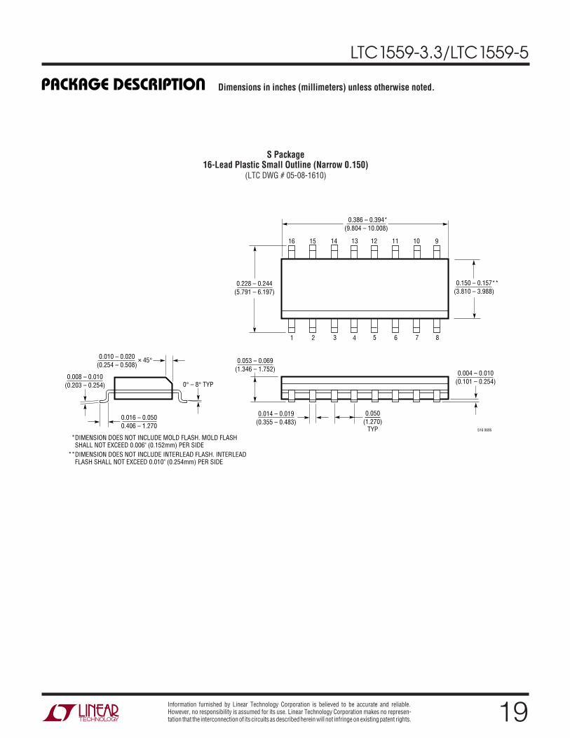
PACKAGE DESCRIPTION
U
Dimensions in inches (millimeters) unless otherwise noted.
1 2 3 4
0.150 – 0.157**(3.810 – 3.988)
8 7 6 5
0.189 – 0.197*(4.801 – 5.004)
0.228 – 0.244(5.791 – 6.197)
0.016 – 0.0500.406 – 1.270
0.010 – 0.020(0.254 – 0.508)
× 45°
0°– 8° TYP0.008 – 0.010
(0.203 – 0.254)
SO8 0996
0.053 – 0.069(1.346 – 1.752)
0.014 – 0.019(0.355 – 0.483)
0.004 – 0.010(0.101 – 0.254)
0.050(1.270)
TYPDIMENSION DOES NOT INCLUDE MOLD FLASH. MOLD FLASH SHALL NOT EXCEED 0.006" (0.152mm) PER SIDEDIMENSION DOES NOT INCLUDE INTERLEAD FLASH. INTERLEAD FLASH SHALL NOT EXCEED 0.010" (0.254mm) PER SIDE
*
**
S8 Package8-Lead Plastic Small Outline (Narrow 0.150)
(LTC DWG # 05-08-1610)

18
LTC1559-3.3/LTC1559-5
PACKAGE DESCRIPTION
U
Dimensions in inches (millimeters) unless otherwise noted.
GN Package16-Lead Plastic SSOP (Narrow 0.150)
(LTC DWG # 05-08-1641)
GN16 (SSOP) 1197
* DIMENSION DOES NOT INCLUDE MOLD FLASH. MOLD FLASHSHALL NOT EXCEED 0.006" (0.152mm) PER SIDE
** DIMENSION DOES NOT INCLUDE INTERLEAD FLASH. INTERLEADFLASH SHALL NOT EXCEED 0.010" (0.254mm) PER SIDE
1 2 3 4 5 6 7 8
0.229 – 0.244(5.817 – 6.198)
0.150 – 0.157**(3.810 – 3.988)
16 15 14 13
0.189 – 0.196*(4.801 – 4.978)
12 11 10 9
0.016 – 0.050(0.406 – 1.270)
0.015 ± 0.004(0.38 ± 0.10)
× 45°
0° – 8° TYP0.007 – 0.0098(0.178 – 0.249)
0.053 – 0.068(1.351 – 1.727)
0.008 – 0.012(0.203 – 0.305)
0.004 – 0.0098(0.102 – 0.249)
0.025(0.635)
BSC
19
LTC1559-3.3/LTC1559-5
PACKAGE DESCRIPTION
U
Dimensions in inches (millimeters) unless otherwise noted.
S Package16-Lead Plastic Small Outline (Narrow 0.150)
(LTC DWG # 05-08-1610)
0.016 – 0.0500.406 – 1.270
0.010 – 0.020(0.254 – 0.508)
× 45°
0° – 8° TYP0.008 – 0.010
(0.203 – 0.254)
1 2 3 4 5 6 7 8
0.150 – 0.157**(3.810 – 3.988)
16 15 14 13
0.386 – 0.394*(9.804 – 10.008)
0.228 – 0.244(5.791 – 6.197)
12 11 10 9
S16 0695
0.053 – 0.069(1.346 – 1.752)
0.014 – 0.019(0.355 – 0.483)
0.004 – 0.010(0.101 – 0.254)
0.050(1.270)
TYPDIMENSION DOES NOT INCLUDE MOLD FLASH. MOLD FLASH SHALL NOT EXCEED 0.006" (0.152mm) PER SIDEDIMENSION DOES NOT INCLUDE INTERLEAD FLASH. INTERLEAD FLASH SHALL NOT EXCEED 0.010" (0.254mm) PER SIDE
*
**
Information furnished by Linear Technology Corporation is believed to be accurate and reliable.However, no responsibility is assumed for its use. Linear Technology Corporation makes no represen-tation that the interconnection of its circuits as described herein will not infringe on existing patent rights.

20
LTC1559-3.3/LTC1559-5
LINEAR TECHNOLOGY CORPORATION 1998
LTC1559-3.3 Backup System with an LTC1435 Main System Regulator(LTC1435 Output Sense at the Source of Q11, LTC1559’s PS Pin Is Grounded)
1559f LT/TP 1098 4K • PRINTED IN USA
PART NUMBER DESCRIPTION COMMENTSLTC690/LTC691 Microprocessor Supervisory Circuits Microprocessor Power Supply Monitor and Backup with Power FailLTC694/LTC695 ComparatorLTC699 Microprocessor Supervisory Circuits Microprocessor Power Supply Monitor and BackupLTC1232 Microprocessor Supervisory Circuits Include Push-Button ResetLTC1235 Microprocessor Supervisory Circuits Include Push-Button Reset and Power Fail ComparatorLTC1149 High Efficiency Synchronous Step-Down VIN up to 48V, Burst ModeTM Operation
Switching RegulatorLTC1435 High Efficiency, Low Noise Synchronous Ultrahigh Efficiency, Burst Mode Operation
Step-Down Switching RegulatorLTC1479 PowerPathTM Controller for Dual Complete Power Management Controller for Battery
Battery Systems Notebook Computers and Other Portable EquipmentLTC1558 Battery Backup Controller with Similar to LTC1559 Except That It Backs up the Main System Regulator’s
Programmable Output Input, Allowing Backup of Multiple Output VoltagesPowerPath and Burst Mode are trademarks of Linear Technology Corporation.
RELATED PARTS
Description
With its SENSE pin at the source of Q11, the LTC1435 canraise VOUT above VCC(rated voltage) – 5.5% once the main
TYPICAL APPLICATION
U
+BG
SENSE–
SENSE+
INTVCC
BOOST
SW
COSC
SGND PGND
RUN/SS
ITH
VOSENSE
VIN
LTC1435
TG
C40.1µF RSENSE**
0.033Ω L1*10µH
*SUMIDA CDRH125-10**IRC LR2010-01-R033-F †SUMIDA CD54-220
C34.7µF16V
D1CMDSH-3
1559 TA04
D2MBRS140T3
R520k1%
R135.7k1%
C51000pF
C6100pF
Q2N-CHSi4412DY
Q1N-CHANNELSi4412DY
SFB
EXTVCC
11
7
8
12
15
14
13
CIN22µF35V× 2
16
5 10
1
2
3
6
4
9
COSC68pF
RC10k
CSS0.1µF
CC330pF
C1100pF
CC251pF
+ C20.1µF
VOUT3.3V
CTL
C111µF6.3V
BACKUPBATTERY1.2VNiCd
MAINBATTERY4.5 TO 28V
Q11P-CHANNELSi9424DY
R1414k
SW
LTC1559-3.3
L11†
22µH
GND
PS
7
1 8
5
6
3
RESETPUSH-BUTTON
2
4
VBAKVCC
RESET
BACKUP
+
R15100k
C121µF
RESET
BACKUP
+
COUT100µF10V×2
+
Linear Technology Corporation1630 McCarthy Blvd., Milpitas, CA 95035-7417(408) 432-1900 FAX: (408) 434-0507 www.linear-tech.com
battery is restored. Thus, the LTC1559 does not use the PSpin to sense the LTC1435’s output during backup mode.The PS pin is grounded in this case. Please refer to theApplications Information section for more details.

Mouser Electronics
Authorized Distributor
Click to View Pricing, Inventory, Delivery & Lifecycle Information: Analog Devices Inc.:
LTC1559CS8-5#TR LTC1559CGN-3.3 LTC1559CGN-5#TR LTC1559CS-5#PBF LTC1559CS8-3.3#PBF
LTC1559CGN-5 LTC1559CS-5#TRPBF LTC1559CS8-3.3#TRPBF LTC1559CS-3.3#PBF LTC1559CGN-3.3#PBF
LTC1559CS8-5#TRPBF LTC1559CS-3.3#TR LTC1559CGN-5#TRPBF LTC1559CS-3.3#TRPBF LTC1559CS-5#TR
LTC1559CS-5 LTC1559CS8-5#PBF LTC1559CS-3.3 LTC1559CGN-3.3#TR LTC1559CGN-3.3#TRPBF
LTC1559CS8-3.3#TR LTC1559CS8-3.3 LTC1559CGN-5#PBF LTC1559CS8-5