DEPFET Pixel: A Pixel Device with Integrated Amplification · DEPFET Pixel: A Pixel Device with...
22
DEPFET Pixel: A Pixel Device with Integrated Amplification Johannes Ulrici Bonn University FAUST Semiconductor Lab Pixel 2000 Conference Genova, 4.6.-8.6. 2000
Transcript of DEPFET Pixel: A Pixel Device with Integrated Amplification · DEPFET Pixel: A Pixel Device with...

DEPFET Pixel: A Pixel Device withIntegrated Amplification
Johannes UlriciBonn University
FAUST Semiconductor Lab
Pixel 2000 Conference Genova, 4.6.-8.6. 2000
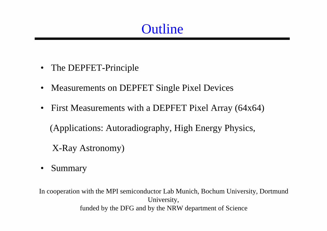
Outline
• The DEPFET-Principle
• Measurements on DEPFET Single Pixel Devices
• First Measurements with a DEPFET Pixel Array (64x64)
(Applications: Autoradiography, High Energy Physics,
X-Ray Astronomy)
• Summary
In cooperation with the MPI semiconductor Lab Munich, Bochum University, DortmundUniversity,
funded by the DFG and by the NRW department of Science

p+
n
pn+
S DG
n+
internal gate
Integration of JFET
DEPFET
Advantage:
• Small input capacitance
• no stray capacitance
=> Large Signal to Noise
Ratio
DEPFET - principle idea
p+
n
n+
pn+
S DG
Sensor Diode
Preamplifier(p-JFET)
Kemmer, Lutz (1987):
• integrate preamplifier into
Sensor Si- Substrate
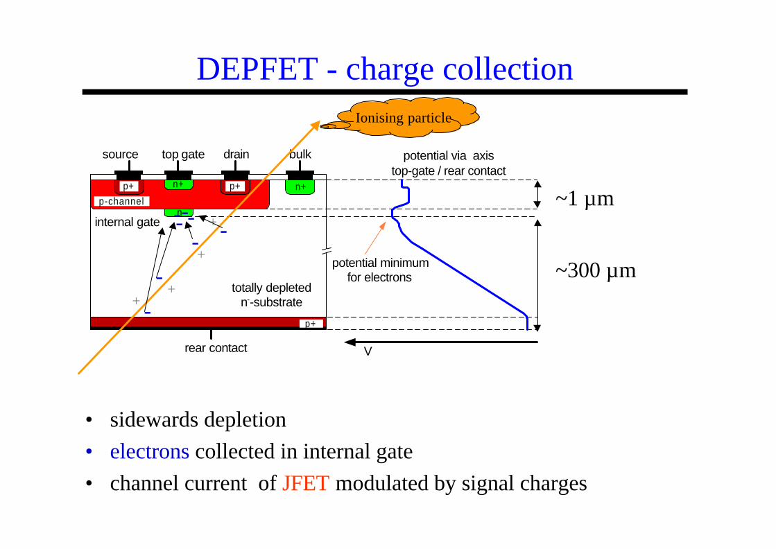
DEPFET - charge collection
• sidewards depletion
• electrons collected in internal gate
• channel current of JFET modulated by signal charges
Ionising particle
p+
p+ n+
n
n+
totally depletedn--substrate
internal gate
rear contact
source top gate drain bulk potential via axistop-gate / rear contact
V
potential minimumfor electrons
p-channelp+
-
-
- -+
+
++
-- --~1 µm
~300 µm

DEPFET - Clear Mechanism
• Internal gate filled bysignal charges andthermally generatedelectrons
• „Reset“ needed
• One possibility: pulsed clear!
• Other clear mechanisms:cont. clear, gate clear, ... p+
p+ n+
rear contact
drain bulksource
p
sym
met
ry a
xis
n+
n
internal gate
top gate clear
n -
n+p+
0V
+15V
0V
pulsed clear: dead time less than 0,1% of measuring time
- -- ---
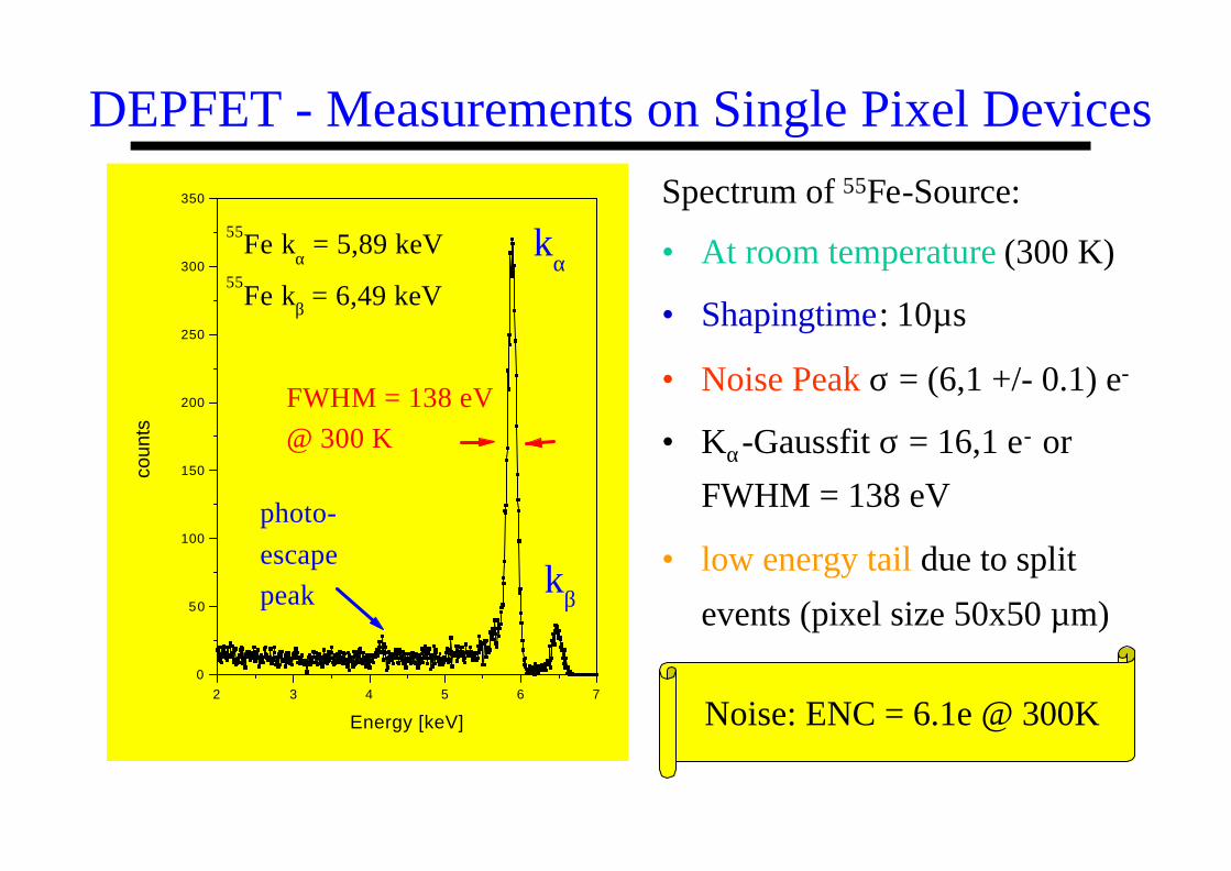
DEPFET - Measurements on Single Pixel Devices
Spectrum of 55Fe-Source:
• At room temperature (300 K)
• Shapingtime: 10µs
• Noise Peak σ = (6,1 +/- 0.1) e-
• Kα-Gaussfit σ = 16,1 e- or
FWHM = 138 eV
• low energy tail due to split
events (pixel size 50x50 µm)
Noise: ENC = 6.1e @ 300K2 3 4 5 6 7
0
50
100
150
200
250
300
350
FWHM = 138 eV
@ 300 K
kβ
kα
photo-
escape
peak
55Fe k
α = 5,89 keV
55Fe kβ = 6,49 keV
coun
ts
Energy [keV]
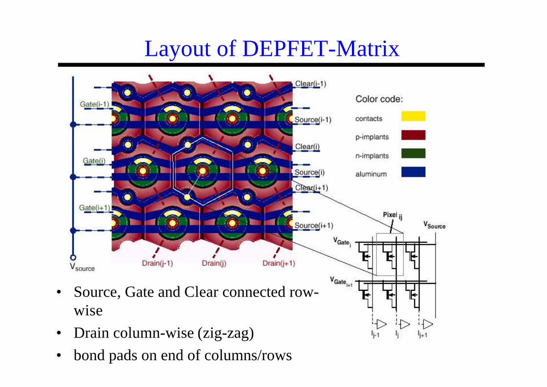
Layout of DEPFET-Matrix
• Source, Gate and Clear connected row-wise
• Drain column-wise (zig-zag)
• bond pads on end of columns/rows

DEPFET - Matrix Data Acquisition
64x64pixel
IDRAIN
DEPFET-matrix
VGATE, OFF
off
off
on
off
VGATE, ON
64-b
it-sh
ift r
egis
ter
gate
drain VCLEAR, OFF
off
off
clear
off
VCLEAR, ON
64-bit-shift register
clear
output
• switch on one row through gate contacts, get pedestal current
• after doing this for all rows, switch row on again, get signal current
clear this row
ext.gate
source
drain
clear
signal charge in int. Gate ~
signal-current -pedestal-current

Developed ASICs:
CARLOS:• low-noise 64-channel amplifier• track & hold• 10 MHz Serializer (64 to 1)
SWITCHER:• 64 channels, 65MHz• AMS 25V HV-technology
DEPFET - Bioscope
64 x 64 DEPFET matrix
CARLOS
Gate-SWITCHER Clear-SWITCHER
further components:• analog PBC with 12-bit ADC• digital PBC with XILINX for data acquisition
1 image (64x64 Pixel) per 1ms

DEPFET Pixel Bioscope System
ADC(12bit)40MHz
FiFo64k x 18bit
Hybrid ADC -Card
PCI - Card(in PCI Slot)
Power SupplyCard
DDC - DigitalDEPFET Card
CARLOS(64
channelAMP &MUX)
SWITCHER(control chip)
SWITCHER(control chip)
64 x 64pulsed clearDEPJFET-
matrix
8
3
1MBstatic RAM
2
XILINX
XIL
INX
32
8
OPAmp
40M
Hz
XILINXXC4010
1512
1 image (64x64 Pixel) per 1ms

The DEPFET Pixel Bioscope

X-Ray images: 64x64 Matrix, 50x50µm2 PixelShadow image of toothed wheel of watch, 55Fe-γ-Source (6keV)
1,2 mm
Pedestal Image
digital information
linear interpolation
0 50 100 150 200 250 300-1000
0
1000
2000
3000
4000
5000
6000
7000
L
M N
O P
R T Total
Sig
nal [
Ele
ktro
nen]
X Achse [µm]
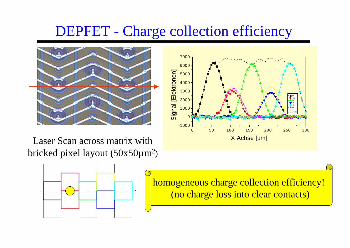
DEPFET - Charge collection efficiency
Laser Scan across matrix withbricked pixel layout (50x50µm2)
homogeneous charge collection efficiency! (no charge loss into clear contacts)

0 10 20 30 40 50 60
0
100
200
300
400
500
600 2 4 1Am
Ba
Tb
Cu
1 0 9Cd Kα
1 0 9Cd Kβ
MoRb
55Fe
AD
C-W
ert
Energie [keV]
DEPFET - linearity and noise
All 4096 Pixels:
-400 -200 0 200 4000
50
100
150
200
250
300
350
400
σGauss
= (119 ± 8) e
Häu
figke
it
Elektronen [e]
B Gauss Fit
very good linearity [6 - 60keV]low noise of single image: σnoise = 84 ±6 e
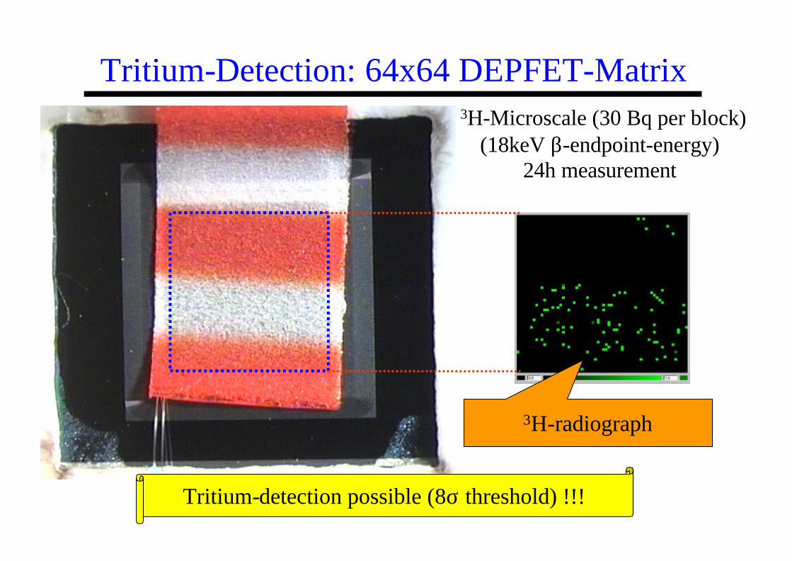
Tritium-Detection: 64x64 DEPFET-Matrix
Tritium-detection possible (8σ threshold) !!!
3H-radiograph
3H-Microscale (30 Bq per block)(18keV β-endpoint-energy)
24h measurement
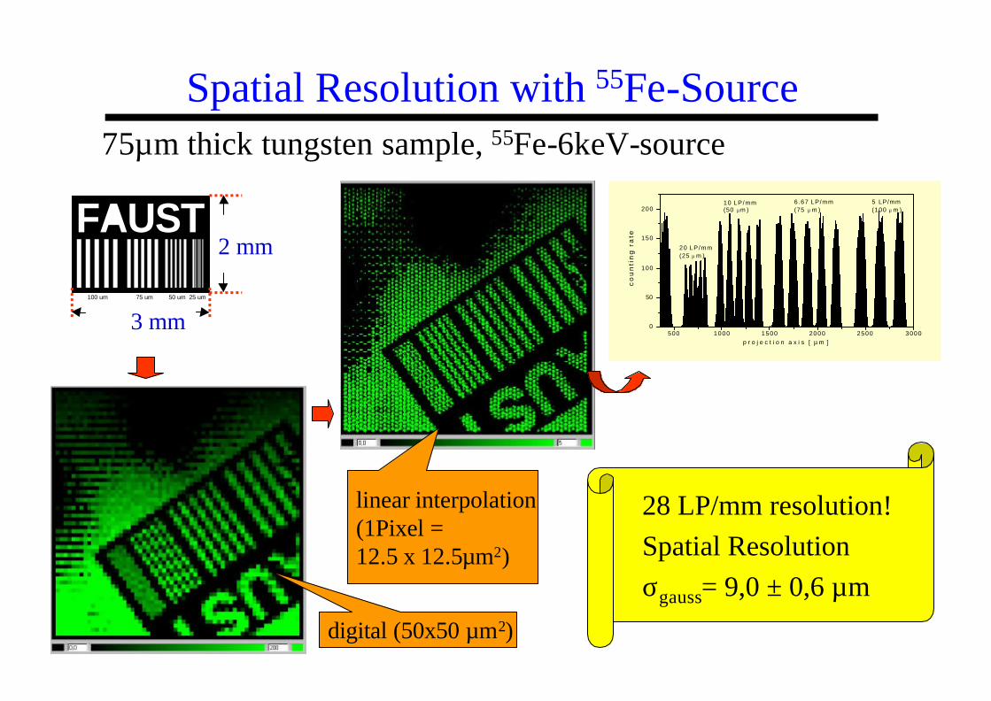
Spatial Resolution with 55Fe-Source75µm thick tungsten sample, 55Fe-6keV-source
500 1000 1500 2000 2500 30000
50
100
150
2006.67 LP/mm(75 µ m )
5 LP/mm(100 µ m )
10 LP/mm(50 µm )
20 LP/mm(25 µ m )
co
un
tin
g r
ate
p r o j e c t i o n a x i s [ µ m ]
digital (50x50 µm2)
FAUST
100 um 50 um 25 um75 um
2 mm
3 mm
linear interpolation(1Pixel =12.5 x 12.5µm2)
28 LP/mm resolution!
Spatial Resolution
σgauss= 9,0 ± 0,6 µm
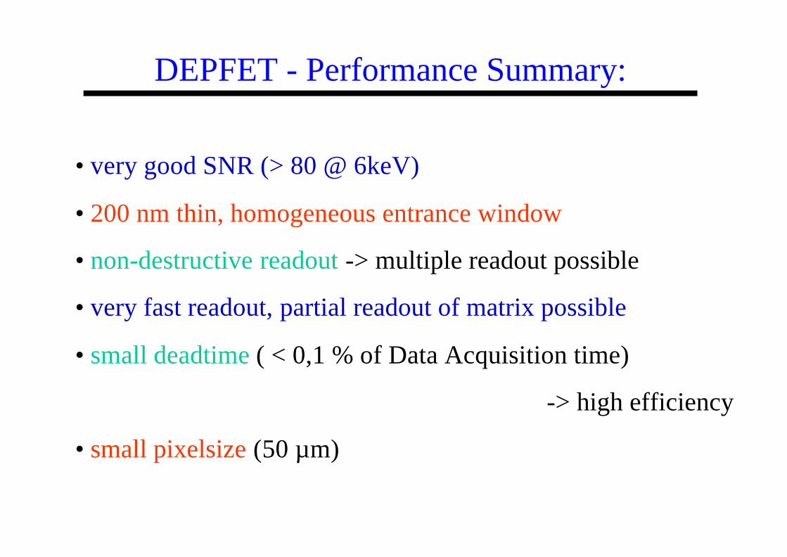
DEPFET - Performance Summary:
• very good SNR (> 80 @ 6keV)
• 200 nm thin, homogeneous entrance window
• non-destructive readout -> multiple readout possible
• very fast readout, partial readout of matrix possible
• small deadtime ( < 0,1 % of Data Acquisition time)
-> high efficiency
• small pixelsize (50 µm)

DEPFET - Applications:Biomedicine (Autoradiography):
• Real time detection of 3H at room temperature without vacuum
• Good energy resolution -> different radioactive markers
X-Ray Astronomy (sucessor of XMM: XEUS)
• low energy γ’s
• high rates, nearly no dead time, no ghost hits
Particle Physics (TESLA)
• thin detectors (30µm)
• small pixel size (30x30 µm2)

Biomedical Application: Autoradiography
Good spatial resolution, no time or energy information
radioactively marked sample
14C: β-decay, 50keV (mean)3H: β-decay, 6keV (mean)
AgBr-Emulsion (d<10µm)
Digital Autoradiography:• time resolved -> real time observation of dynamic processes -> no development of film necessary (up to months)
-> not sensitive to exposure time• energy resolution -> different radioactive markers• DEPFET -> detection of 3H (room temperature, no vacuum!)
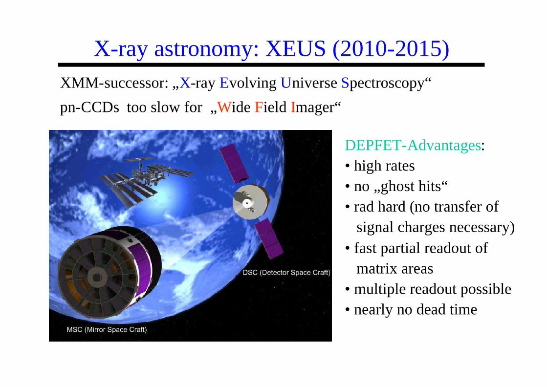
X-ray astronomy: XEUS (2010-2015)XMM-successor: „X-ray Evolving Universe Spectroscopy“
pn-CCDs too slow for „Wide Field Imager“
DEPFET-Advantages:• high rates• no „ghost hits“• rad hard (no transfer of signal charges necessary)• fast partial readout of matrix areas• multiple readout possible• nearly no dead time

Summary
• DEPFET- single pixel:– ENC = 6,1 e @ room temperature
• DEPFET Pixel Bioscope with 64 x 64 DEPFETMatrix:– Readout time for 1 image: ~ 1ms
– spatial resolution with simple linear interpolation: ~ 9µm– noise of single image > 10 e
– Tritium detected!
– homogeneous charge collection efficiency!
• future: time resolved
measurements, various applications

DEPFET: InformationRecent papers:
W. Neeser, M. Böcker, P. Buchholz, P. Fischer, P. Holl, J. Kemmer, P. Klein, H. Koch, M. Löcker, G. Lutz, H. Matthäy, L. Strüder, M. Trimpl, J. Ulrici, N. Wermes; "DEPFET - a pixel device with integrated amplification", submitted to NIM A
W. Neeser, M. Böcker, P. Buchholz, P. Fischer, P. Holl, J. Kemmer, P. Klein, H. Koch, M. Löcker, G. Lutz, H. Matthäy, L. Strüder, M. Trimpl, J. Ulrici, N. Wermes; "The DEPFET Pixel Bioscope", submitted to IEEE Trans. on Nucl. Sci.
P. Klein, T. Aurisch, P. Fischer, W. Neeser, L. Strüder, M. Trimpl, J. Ulrici, J. Vocht, N. Wermes; "A DEPFET Pixel Bioscope for the Use in Autoradiography", submitted to NIM A
Homepage:
depfet.physik.uni-bonn.de