
Department of Electronics Introductory Nanotechnology ~ Basic Condensed Matter Physics ~ Atsufumi...
27
Department of Electronics Introductory Nanotechnology ~ Basic Condensed Matter Physics ~ Atsufumi Hirohata
-
Upload
russell-james -
Category
Documents
-
view
218 -
download
2
Transcript of Department of Electronics Introductory Nanotechnology ~ Basic Condensed Matter Physics ~ Atsufumi...

Department of Electronics
Introductory Nanotechnology
~ Basic Condensed Matter Physics
~
Atsufumi Hirohata

Quick Review over the Last Lecture
Classic model : Dulong-Petit empirical law
T
c V, mol
3R
0 E
DEinstein model :
• E : Einstein temperature
• c V, mol ~ 3R for E << T
• c V, mol exp (- E / T) for E << T
Debye model :
• D : Debye temperature
• c V, mol ~ 3R for D << T
• c V, mol T 3 for D << T

Contents of Introductory Nanotechnology
First half of the course : Basic condensed matter physics
1. Why solids are solid ?
2. What is the most common atom on the earth ?
3. How does an electron travel in a material ?
4. How does lattices vibrate thermally ?
5. What is a semi-conductor ?
6. How does an electron tunnel through a barrier ?
Second half of the course : Introduction to nanotechnology (nano-fabrication / application)
7. Why does a magnet attract / retract ?
8. What happens at interfaces ?

What Is a Semi-Conductor ?
• Elemental / compound semiconductor
• Intrinsic / extrinsic semiconductors
• n / p-dope
• Temperature dependence
• Schottky junctions
• pn junctions

What is semi-conductor ?
Band diagrams :
metal conductors insulators
Forbidden
Allowed
Allowed
semiconductors
Forbidden
Allowed
Allowed
Forbidden
AllowedForbidden
Allowed
Allowed
With very small energy,
electrons can overcome
the forbidden band.
EF

Energy Band of a semiconductor
Schematic energy band diagram :
E
Conduction band
Valence band
Band gapconduction electron
hole
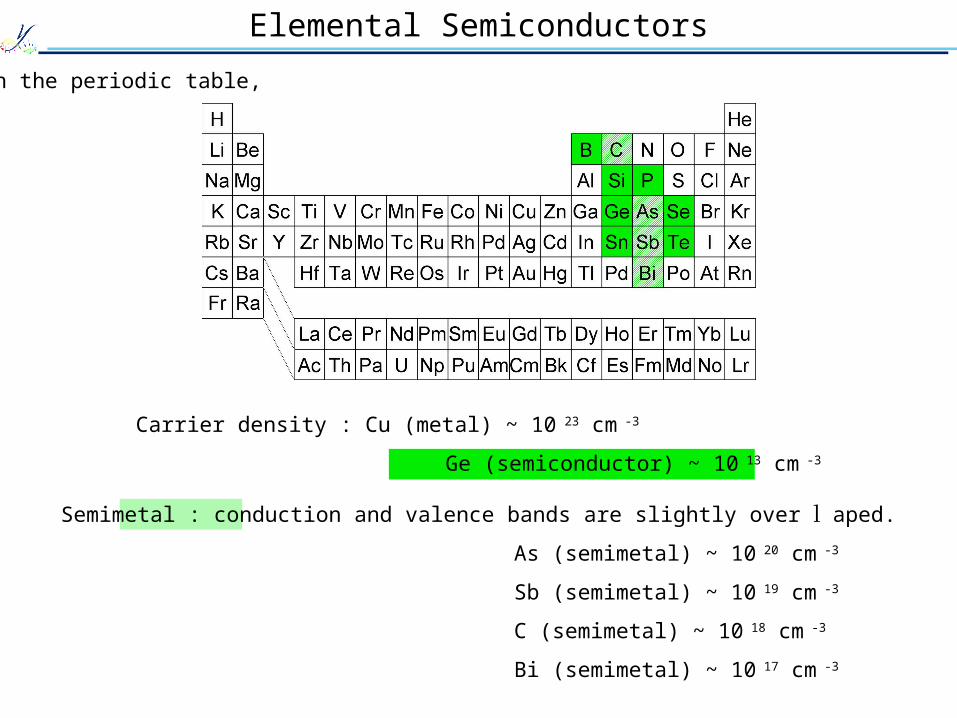
Elemental Semiconductors
In the periodic table,
Semimetal : conduction and valence bands are slightly over l aped.
As (semimetal) ~ 10 20 cm -3
Sb (semimetal) ~ 10 19 cm -3
C (semimetal) ~ 10 18 cm -3
Bi (semimetal) ~ 10 17 cm -3
Carrier density : Cu (metal) ~ 10 23 cm -3
Ge (semiconductor) ~ 10 13 cm -3

Fabrication of a Si-Based Integrated Circuit
Czochralski method :Si purity (99.999999999 %)
* http://www.wikipedia.org/

Compound Semiconductors
In the periodic table,
III-V compounds : GaAs, InAs, InSb, AlP, BP, ...
II-VI compounds : ZnO, CdS, CdTe, ...
IV-IV compounds : SiC, GeSi
IV-VI compounds : PbSe, PbTe, SnTe, ...
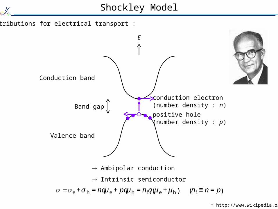
Shockley Model
Contributions for electrical transport :
E
Conduction band
Valence band
Band gapconduction electron (number density : n)
positive hole(number density : p)
Ambipolar conduction
Intrinsic semiconductor
€
σ =σ e +σ h = nqμ e + pqμ h = niq μ e + μ h( ) n i ≡ n = p( )
* http://www.wikipedia.org/
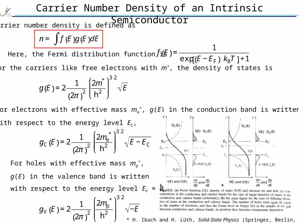
Carrier Number Density of an Intrinsic Semiconductor
Carrier number density is defined as
€
n = f E( )g E( )dE∫Here, the Fermi distribution function is
€
f E( ) =1
exp E − EF( ) kBT[ ] +1For the carriers like free electrons with m*, the density of states is
€
g E( ) = 21
2π( )2
2m*
h2
⎛
⎝ ⎜
⎞
⎠ ⎟
3 2
E
For electrons with effective mass me*, g(E) in the conduction band is written
with respect to the energy level EC,
* H. Ibach and H. Lüth, Solid-State Physics (Springer, Berlin, 2003).
€
gC E( ) = 21
2π( )2
2me*
h2
⎛
⎝ ⎜ ⎜
⎞
⎠ ⎟ ⎟
3 2
E − EC
For holes with effective mass mp*,
g(E) in the valence band is written
with respect to the energy level EV = 0,
€
gV E( ) = 21
2π( )2
2mp*
h2
⎛
⎝ ⎜ ⎜
⎞
⎠ ⎟ ⎟
3 2
−E

Carrier Number Density of an Intrinsic Semiconductor (Cont'd)
fp(E) for holes equals to the numbers of unoccupied states by electrons :
€
fp E( ) = 1− fe E( )
n is an integral in the conduction band from the bottom EC to top Ect :
€
n = fe E( )ge E( )dEEC
ECt∫ =1
2π 2
2me*
h2
⎛
⎝ ⎜ ⎜
⎞
⎠ ⎟ ⎟
3 2
E − EC1
exp E − EF( ) kBT[ ] +1dE
EC
ECt∫p is an integral in the valence band from the bottom -EVb to top 0 :
€
p = fp E( )gp E( )dE−EVb
0
∫ =1
2π 2
2mp*
h2
⎛
⎝ ⎜ ⎜
⎞
⎠ ⎟ ⎟
3 2
−E 1−1
exp E − EF( ) kBT[ ] +1
⎧ ⎨ ⎪
⎩ ⎪
⎫ ⎬ ⎪
⎭ ⎪dE
−Evb
0
∫
=1
2π 2
2mp*
h2
⎛
⎝ ⎜ ⎜
⎞
⎠ ⎟ ⎟
3 2
−E1
exp − E − EF( ) kBT[ ] +1dE
−Evb
0
∫
Here, EC (= Eg = EC - EV) >> kBT E - EF EC /2 for EC E Ect (EF ~ EC /2)
€
fe E( ) ≈ exp − E − EF( ) kBT[ ]
Similarly, EC >> kBT -(E - EF) EC /2 for EVb E 0
€
fp E( ) ≈ exp E − EF( ) kBT[ ]

Carrier Number Density of an Intrinsic Semiconductor (Cont'd)
For E - EF > 3kBT,
€
fe EF + 3kBT( ) < 0.05 and hence ECt ∞
Similarly,
€
fp EF − 3kBT( ) < 0.05 and hence EVb -∞
€
n =1
2π 2
2me*
h2
⎛
⎝ ⎜ ⎜
⎞
⎠ ⎟ ⎟
3 2
E − EC exp − E − EF( ) kBT[ ]dEEC
∞
∫
€
p =1
2π 2
2mp*
h2
⎛
⎝ ⎜ ⎜
⎞
⎠ ⎟ ⎟
3 2
−E exp E − EF( ) kBT[ ]dE−∞
0
∫As a result,
€
n = NC exp − EC − EF( ) kBT[ ] ≈ NC fe EC( )
€
NC ≡ NCeT3 2
NCe ≡ 22πme
*kB
h2
⎛
⎝ ⎜ ⎜
⎞
⎠ ⎟ ⎟
3 2
⎧
⎨ ⎪ ⎪
⎩ ⎪ ⎪
€
n = NV exp −EF kBT[ ] ≈ NV fp 0( )
€
NV ≡ NVpT3 2
NVp ≡ 22πmp
*kB
h2
⎛
⎝ ⎜ ⎜
⎞
⎠ ⎟ ⎟
3 2
⎧
⎨ ⎪ ⎪
⎩ ⎪ ⎪

Fermi Level of an Intrinsic Semiconductor
For an intrinsic semiconductor,
€
n = p ≡ ni
€
NC exp − EC − EF( ) kBT[ ] = NV exp −EF kBT[ ]
€
∴EF =1
2EC +
3
4kBT ln
mp*
me*
⎛
⎝ ⎜ ⎜
⎞
⎠ ⎟ ⎟
Assuming, me* = mp
* = m*
€
EF =1
2EC =
1
2Eg
np product is calculated to be
€
np = ni2 = NCNV exp −EC kBT[ ] = 4
2πkBT
h2
⎛
⎝ ⎜
⎞
⎠ ⎟3
me*mp
*( )
3 2exp −EC kBT( )
constant for small ni
can be applied for an extrinsic (impurity) semiconductor

Extrinsic Semiconductors
Doping of an impurity into an intrinsic semiconductor :
n-type extrinsic semiconductor :
e.g., Si (+ P, As, Sb : donor)
* M. Sakata, Solid State Physics (Baifukan, Tokyo, 1989).
p-type extrinsic semiconductor :
e.g., Si (+ Ga, Al, B : acceptor)
As neutral donorAs positive donor
conduction electron
conduction band
B neutral acceptorholes
B negative acceptor

Carrier Number Density of an Extrinsic Semiconductor
Numbers of holes in the valence band EV should equal to
the sum of those of electrons in the conduction band EC and in the acceptor level EA :
€
p = n + nA
Similar to the intrinsic case,
€
p = NV fp 0( ) ≈ NV exp −EF
kBT
⎛
⎝ ⎜
⎞
⎠ ⎟
€
n = NC fe Eg( ) ≈ NC exp −Eg − EF
kBT
⎛
⎝ ⎜
⎞
⎠ ⎟
Assuming numbers of neutral acceptors are NA,
€
nA =NA
1 + 2expEA − EF
kBT
⎛
⎝ ⎜
⎞
⎠ ⎟
valence band
EC (Eg)
EF
EA
EV (0)
n
nA
p
For EA - EF > kBT,
€
nA ≈ NA
€
∴NV exp −EF
kBT
⎛
⎝ ⎜
⎞
⎠ ⎟≈ NC exp −
Eg − EF
kBT
⎛
⎝ ⎜
⎞
⎠ ⎟+NA

Carrier Number Density of an Extrinsic Semiconductor (Cont'd)
At low temperature, one can assume p >> n,
€
p ≈ nA
As nA is very small, EA > EF
€
nA =NA
2exp −
EA − EF
kBT
⎛
⎝ ⎜
⎞
⎠ ⎟
€
∴NV exp −EF
kBT
⎛
⎝ ⎜
⎞
⎠ ⎟≈NA
2exp −
EA − EF
kBT
⎛
⎝ ⎜
⎞
⎠ ⎟
€
∴exp −EF
kBT
⎛
⎝ ⎜
⎞
⎠ ⎟≈
NA
2NV
exp −EA
2kBT
⎛
⎝ ⎜
⎞
⎠ ⎟
€
∴EF ≈kBT
2ln
2NV
NA
+EA
2
€
NV ≡ NVpT3 2
By substituting
€
∴EF ≈kBT
2ln
2NVp
NA
T 3 2 ⎛
⎝ ⎜
⎞
⎠ ⎟+EA
2
For T ~ 0,
€
EF ≈EA
2
valence band
EC (Eg)
EA
EF
EV (0)
n
p
nA
At high temperature, one can assume n >> nA,
€
p ≈ n
Similar to the intrinsic case, for me* = mp
*,
€
EF ≈Eg
2
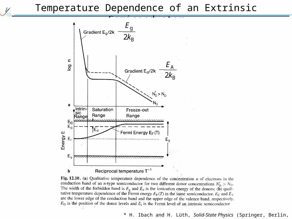
Temperature Dependence of an Extrinsic Semiconductor
* H. Ibach and H. Lüth, Solid-State Physics (Springer, Berlin, 2003).
€
−Eg
2kB
€
−EA
2kB

Semiconductor Junctions
Work function :
Na 11+
1s
2s
2p3s
vacuum level
EF
Current density of thermoelectrons :
€
J = AT 2 exp −φ
kBT
⎛
⎝ ⎜
⎞
⎠ ⎟
Richardson-Dushman equation
A : Richardson constant (~120 Acm 2/K)
Metal - metal junction :
vacuum level
A B
EFA
EFB A - B
= EFA - EFB
A - B : contact potential ---
+ + +vacuum level
A B
EFA
EFB
EFA = EFB
A B
EFA EFB
A B
barrier

Metal - Semiconductor Junction - n-Type
Metal - n-type semiconductor junction :
vacuum level
M
S : electron affinity
EFM
EFS
Mn-S
EV : valence band
ED : donor levelEC : conduction band
S
qVd = M - S : Schottky barrier height
EFM EFS
Mn-S
EV
ED
EC M - S ----+ + + +
depletion layer
* http://www.dpg-physik.de/

Metal - Semiconductor Junction - p-Type
Metal - p-type semiconductor junction :
vacuum level
M S : electron affinity
EFM
Mp-S
EV
EC S
qVd = S - M
EFM EFS
Mp-S
EV
EC
S - M ++++
depletion layer
EA : acceptor levelEFS
EA

Einstein Relationship
At the equillibrium state,
Numbers of electrons diffuses towards -x direction are
€
−Dedn
dx
(n : electron number density, De : diffusion coefficient)
EF
ED
EC
EV
x
Drift velocity of electrons with mobility e under E is
€
vd = −μ eE
Numbers of electrons travel towards +x direction under E are
€
nvd = −μ enE
As E is generated by the gradient of EC, E is along -x and vd is +x.
(-x direction)
(+x direction)
€
−enE −Dedn
dx= 0 (equillibrium state)
Assuming EV = 0, electron number density is defined as
€
n = N e exp −EC − EF
kBT
⎛
⎝ ⎜
⎞
⎠ ⎟

Einstein Relationship (Cont'd)
Now, an electric field E produces voltage VCF = VC - VF
€
EC − EF = −qVCF = −q VC −VF( )
€
∴E = −dVCF
dx=
1
q
d EC − EF( )
dx
Accordingly,
€
dn
dx=
dn
d EC − EF( )⋅d EC − EF( )
dx= −
1
kBTn ⋅qE
€
∴enE = DenqE
kBT
€
∴De = μ ekBT
q Einstein relationship
Therefore, a current density Jn can be calculated as
€
Jn = − −qμ enE − qDedn
dx
⎛
⎝ ⎜
⎞
⎠ ⎟= qDe −
qn
kBT⋅dVxdx
+dn
dx
⎛
⎝ ⎜
⎞
⎠ ⎟
€
∴Jn = B exp −q Vd −V( )
kBT
⎛
⎝ ⎜
⎞
⎠ ⎟− exp −
qVd
kBT
⎛
⎝ ⎜
⎞
⎠ ⎟
⎡
⎣ ⎢ ⎢
⎤
⎦ ⎥ ⎥

Rectification in a Schottky Junction
By applying a bias voltage V onto a metal - n-type semiconductor junction :
* H. Ibach and H. Lüth, Solid-State Physics (Springer, Berlin, 2003).
forward bias
reverse bias
M - S q(Vd - V)
€
JFoward = JM→S − JS→M = B exp −q Vd −V( )
kBT
⎛
⎝ ⎜
⎞
⎠ ⎟− exp −
qVd
kBT
⎛
⎝ ⎜
⎞
⎠ ⎟
⎡
⎣ ⎢ ⎢
⎤
⎦ ⎥ ⎥
= J0 expqV
kBT
⎛
⎝ ⎜
⎞
⎠ ⎟−1
⎡
⎣ ⎢
⎤
⎦ ⎥≈ J0 exp
qV
kBT
⎛
⎝ ⎜
⎞
⎠ ⎟ V : large( )
M - S q(Vd - V)
€
JReverse = JM→S − JS→M = B exp −q Vd +V( )
kBT
⎛
⎝ ⎜
⎞
⎠ ⎟− exp −
qVd
kBT
⎛
⎝ ⎜
⎞
⎠ ⎟
⎡
⎣ ⎢ ⎢
⎤
⎦ ⎥ ⎥
= J0 exp −qV
kBT
⎛
⎝ ⎜
⎞
⎠ ⎟−1
⎡
⎣ ⎢
⎤
⎦ ⎥≈ J0 V : large( )
J
V
€
JFoward = J0 expqV
kBT
⎛
⎝ ⎜
⎞
⎠ ⎟
€
JReverse = J0
pn Junction
Fabrication method :
• Annealing method :
n-type : Spread P2O5 onto a Si substrate and anneal in forming gas.
p-type : Spread B2O3 onto a Si substrate and anneal in forming gas.
• Epitaxy method (“epi” = on + “taxy” = arrangement) :
Oriented overgrowth
n-type : thermal deformation of SiH4 (+ PCl3) on a Si substrate
p-type : thermal deformation of SiH4 (+ BBr3) on a Si substrate
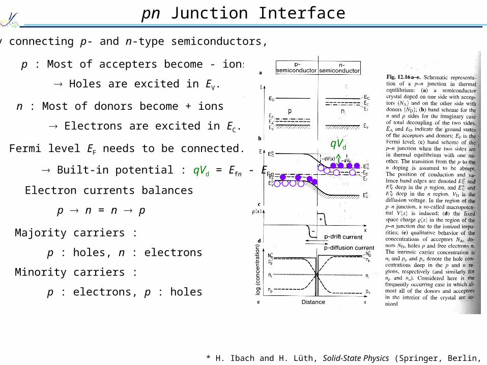
pn Junction Interface
By connecting p- and n-type semiconductors,
p : Most of accepters become - ions
Holes are excited in EV.
* H. Ibach and H. Lüth, Solid-State Physics (Springer, Berlin, 2003).
Fermi level EF needs to be connected.
Built-in potential : qVd = Efn - EFp
n : Most of donors become + ions
Electrons are excited in EC.
qVd
Electron currents balances
p n = n p
Majority carriers :
p : holes, n : electrons
Minority carriers :
p : electrons, p : holes

Rectification in a pn Junction
Under an electrical field E,
Current rectification :
** H. Ibach and H. Lüth, Solid-State Physics (Springer, Berlin, 2003).* M. Sakata, Solid State Physics (Baifukan, Tokyo, 1989).
hole electron
forward bias
drift current
hole
reverse bias
very small drift current


![Introduction to Nanotechnology What is Nanotechnology While many definitions for nanotechnology exist, the [National Nanotechnology Initiative] NNI calls.](https://static.fdocuments.us/doc/165x107/56649d9e5503460f94a88dbf/introduction-to-nanotechnology-what-is-nanotechnology-while-many-definitions.jpg)