DEPARTMENT OF CONDENSED MATTER PHYSICS AND …
14
DEPARTMENT OF CONDENSED MATTER PHYSICS AND MATERIALS SCIENCE Welcome to the Department of Condensed Matter Physics and Materials Science (CMPMS) at TIFR! Research in CMPMS asks questions about the nature of materials that are in the “condensed state” – familiar condensed phases like solids or liquids, but also more exotic phases such as the superconducting phase at low temperatures, magnetically-ordered phases etc. We also work on semiconductors and nanostructured materials, and soft-matter. We study the electronic, physical, mechanical, optical, and chemical properties of materials, in relation to their structure. Our emphasis is on the experimental measurement of various properties using different probes in an attempt to understand the underlying physical behaviour. We fabricate optoelectronic, plasmonic, and superconducting device structures that serve as test sytems to study novel phenomena and also enable real world applications. Tata Institute of Fundamental Research, Homi Bhabha Road, Colaba, Mumbai 400005, India www.tifr.res.in/~dcmpms/ Faculty Members Pushan Ayyub, Chair Venugopal Achanta Shobo Bhattacharyya Arnab Bhattacharya Mandar Deshmukh Sudesh Kumar Dhar Sandip Ghosh Shankar Ghosh A K Grover ( on lien ) Kalobaran Maiti Arun Kumar Nigam P L Paulose Shriganesh Prabhu S Ramakrishnan Pratap Raychaudhuri E V Sampathkumaran A Thamizhavel R Vijayaraghavan
Transcript of DEPARTMENT OF CONDENSED MATTER PHYSICS AND …

D E PA R T M E N T O F C O N D E N S E D M AT T E R P H Y S I C S
A N D M AT E R I A L S S C I E N C E
Welcome to the Department of Condensed Matter
Physics and Materials Science (CMPMS) at TIFR!
Research in CMPMS asks questions about the nature
of materials that are in the “condensed state” –
familiar condensed phases like solids or liquids, but
also more exotic phases such as the superconducting
phase at low temperatures, magnetically-ordered
phases etc. We also work on semiconductors and
nanostructured materials, and soft-matter. We study
the electronic, physical, mechanical, optical, and
chemical properties of materials, in relation to their
structure. Our emphasis is on the experimental
measurement of various properties using different
probes in an attempt to understand the underlying
physical behaviour. We fabricate optoelectronic,
plasmonic, and superconducting device structures
that serve as test sytems to study novel phenomena
and also enable real world applications.
Tata Institute of Fundamental Research, Homi Bhabha Road, Colaba, Mumbai 400005, India
www.tifr.res.in/~dcmpms/
F a c u l t y M e m b e r s
P u s h a n A y y u b , C h a i r
V e n u g o p a l A c h a n t a
S h o b o B h a t t a c h a r y y a
A r n a b B h a t t a c h a r y a
M a n d a r D e s h m u k h
S u d e s h K u m a r D h a r
S a n d i p G h o s h
S h a n k a r G h o s h
A K G r o v e r ( o n l i e n )
K a l o b a r a n M a i t i
A r u n K u m a r N i g a m
P L P a u l o s e
S h r i g a n e s h P r a b h u
S R a m a k r i s h n a n
P r a t a p R a y c h a u d h u r i
E V S a m p a t h k u m a r a n
A T h a m i z h a v e l
R V i j a y a r a g h a v a n

Condensed Matter Physics & Materials Science
Research areas
A common question across various research groups is how electrons organize themselves
in different materials giving rise to a host of interesting physical phenomena. Strongly
correlated electrons are responsible for many phenomena in solid-state physics,
especially in the areas of magnetism and superconductivity, and physics at ultra-low
temperatures. In semiconductors, confining electrons to very tiny nanometer-sized
regions in thin sheets, narrow wires, or small boxes results in quantum wells, wires and
dots, where their properties are modified by quantum mechanical effects in dramatic and
potentially useful ways. The interaction between an electromagnetic field and free
electrons in a metal can result in coherent electron oscillations at the interface –
“plasmonics” tries to study and make use of these oscillations by patterning materials at
the nanoscale. Superconductors can be used to build electrical circuits engineered to
behave like quantum two level systems for applications in quantum computing.
On the materials science side, we study the electronic, physical, mechanical, optical, and
chemical properties of materials, most often in relation to their structure, and use this
knowledge to understand and optimize their properties and create new, improved
materials and devices. Increasingly, the functionality of modern materials depends on
control of their structure at the atomic scale. “Soft” condensed matter research explores
areas like adhesion, friction, wetting, and the movement of fluids in porous media etc.
Experimental facilities
From exploring basic materials properties to the fabrication of advanced electronic, nano-
mechanical, and optoelectronic devices, the experimental facilities in CMPMS are
comparable to the best world-wide. These include materials synthesis facilities like single-
crystal growth, epitaxial deposition of semiconductors, chemical vapour deposition of
graphene, pulsed laser deposition, sputtering and other thin-film growth techniques.
Characterization tools range from optical spectroscopies such as photoluminescence and
Raman scattering to ultrafast time-resolved pump-probe measurements with samples being
probed from the UV through the visible/IR and into the THz region.
Structural properties are determined using high-resolution x-ray diffraction, ultra-high-
resolution electron microscopy, scanning tunneling microscopy and other scanning probe
techniques. For measurements of the electronic and magnetic properties SQUID and other
sensitive magnetometers, high-resolution and spin-resolved photoemission spectroscopy,
and precision transport studies at ultra-low temperatures, in individual nanostructures and
up to the GHz frequency range are available. The soft-condensed matter lab has setups for
imaging complex fluid flows. We also have a small but well-equipped clean room for micro
and nano-fabrication including optical and electron-beam lithography, plasma etching,
thermal and electron-beam deposition, atomic layer deposition, etc.
A world of opportunities
From superconductors and magnetic materials, to semiconductors and nanostructured
metals, research in CMPMS covers a diverse range of “matter that matters” in today’s
world. The diversity of systems and phenomena available for study makes condensed
matter physics the most active field of contemporary physics today. Not surprisingly, it is
also the area of physics with the widest choice of job prospects, and our graduate students
have gone on to exciting careers in academia and industry across the world.
The following pages provide a snapshot of some of the work being done in our
department. Feel free to contact individual faculty members and find out more about their
research. You can also find more information on our website: www.tifr.res.in/~dcmpms/
We hope you will have fun exploring CMPMS@TIFR!

Nanomaterials Research Laboratory
A Transmission Electron Microscope
used for imaging nanostructures
GROUP MEMBERS:
P.I.: Pushan Ayyub
PhD students: Indrani
Chakraborty, Anirban Pal,
Subhrangsu Sarkar
Staff Members: Smita Gohil,
Nilesh Kulkarni (XRD Lab)
PhD and Post-Doc positions
available
Lab: AB-93
Phone: (022) 2278 2295
E-mail: [email protected]
URL: www.tifr.res.in/~pushan/
The NanoLab: What do we study?
Most physical and chemical properties of matter change, often quite drastically, when the physical size of the sample is made smaller than 10-100 nanometer (nm). We are interested in finding out how and why different properties change (“finite size effects”) in nanostructured solids. We try to address and understand simple questions such as:
m Does a superconducting material in the form of a nanoparticle retain superconductivity?
m What is the colour of Silver in the form of nanoparticles?
m How can one make a solar cell out of an array of nanorods?
m Does crystal structure change when particle size is reduced?
Selected results from the NanoLab
Simultaneous ferromagnetism & ferroelectricity in Se microtubes
Multiferroic materials, in which ferromagnetism and ferroelectricity are
intrinsically coupled, have generated much interest. We have observed a
coexistence of magnetic and ferroelectric ordering in single crystalline
Selenium microtubes (Fig. 1) below 40K. This is the first time that
multiferroicity has been observed in a simple element. This unexpected
behavior arises from Selenium being a ‘surface topological insulator’. Reference: Pal et al., Scientific Reports 3 (2013) 2051
A new form of Silver stabilized by small particle size
By carefully controlling the particle size, we have made a new form of
silver with a hexagonal crystal structure (normal silver is cubic) and
surprisingly different properties. Hex silver is golden in colour (Fig. 2) and
has a high electrical resistance. It is chemically reactive, hard and brittle. Reference: Chakraborty et al., J. Physics Con. Mat. 23 (2011) 325401; J. Physics Con.
Mat. 26 (2014) 025402
Clustered metal nanorod arrays: Exciting applications
We have shown that an array of parallel, metallic nanorods (Fig. 3) can
act as an electrode for ultra-low voltage gas discharge [Nanotechnology 19
(2008) 445713], is an excellent source for field-induced electron emission, as
well as laser-induced emission of pulsed, hard x-rays [Physical Review B 83
(2011) 035408].
Experimental Techniques
We make nanoparticles, nano-
crystalline thin films and arrays of
aligned nanorods by high
pressure sputtering, chemical and
electrochemical techniques. The
nanostructured samples are
characterized by high resolution
electron microscopy, x-ray
diffraction, etc. Physical property
measurement techniques involve
Raman and optical spectroscopy,
electrical transport, magnetism,
thermal analysis, and so on.
Fig. 1 Fig. 2 Fig.3

Fundamental Optics, THz & Optical Nanostructures
FDTD simulation
results showing
field localization
at the interface.
Tools & Techniques
Numerical Design tools: finite
difference time domain, rigorous
coupled wave analysis, finite element.
Fabrication tools: photo-, e-beam,
interference- lithography and wet or
dry etching methods.
Optical spectroscopy tools: linear and
nonlinear techniques with 1 µm
spatial-, sub-nanosec time-, 0.1 nm
wavelength- resolution.
Welcome to Foton lab: Plasmonics and Photonics Activity
In the Foton lab we are active in the areas of Plasmonics
and Photonics. We investigate light modulation and control
of optical properties in nanopatterned metal-dielectric and
dielectrics. Broadband response is of particular interest.
Nanopatterns conforming to crystals, quasicrystals or
aperiodic patterns are designed to have unique properties.
We fabricate and study these structures.
We study light localization for quantum information
processing, controlling light emission and light modulation
for nanophotonic and optical planar integrated circuits and
modulation of optical properties of materials.
Metamaterials (Plasmonic)
Surface plasmon polaritons (SPPs) are charge density waves at the metal-
dielectric interface. SPP excitation and resultant strong local field is useful
for manipulating the optical properties of materials and light itself. We
design, fabricate and study metal-dielectric structures.
With emphasis on light harvesting, broadband and near dispersionless
plasmon excitation is demonstrated in plasmonic crystals and
quasicrystals.
We demonstrated plasmon mediated giant enhancement of magneto-
optical properties. Enhanced light emission from semiconductors and light
modulation in plasmonic crystals are some of the topics we are currently
working on.
Light reflected at an interface experiences various shifts like Goos-
Hanchen, Imbert-Federov and angular shifts. We designed and
demonstrated structures that exhibit giant plasmon mediated beam shifts.
Dielectric structures
Photonic crystals, periodic dielectric structures, are actively pursued. PC
cavities with quantum dot defects are studied for quantum information
processing.
All dielectric metamaterials conforming to Reflectionless potentials are
demonstrated for broadband reflectionless transmission.
Cross waveguides about single quantum dots demonstrated for measuring
the complete polarization state of the emitted light.
Plasmonic Quasicrystal air hole pattern
Cross waveguides
having a single
quantum dot at the
intersection
CURRENT MEMBERS:
Prof. Achanta Venu Gopal,
Gajendra Mulay, Dr. Nageswara
Rao, Y.V. Jayasurya, Ajith P.R.,
Banoj Kumar Naik, Richa Goel
1 PhD position available
Lab: C235 / C225 E-mail:
[email protected] Phone:
022-22782910 url:
www.tifr.res.in/~Foton/

CURRENT MEMBERS:
Prof. Shankar Ghosh,
Prof. Shobo Bhattacharya,
PhD positions available? YES
Lab: BB30
E-mail:
Phone: 022-22782445
Welcome to the Soft Matter Lab!
The soft matter research program is mainly inspired by our
experience with interesting but non-intuitive phenomena with
everyday materials, such as peeling of paint, sticking of
particulate matter to surfaces, formation of cloud, structure and
dynamical response of a sandpile. Questions of basic and general
nature are extracted from them and experimental methods are
devised in order to find precise answers about them in model
systems that retain the essence of the original observations. The
experimental systems typically consist of building blocks that are
larger than atomic dimensions, from ten nanometers to
centimeters, both in and out of mechanical and
thermodynamically equilibrium. The investigations are aimed to
provide deeper understanding of the world around us. We use
experimental tools like optical tweezers, various types of
rheometry and high speed imaging techniques. We also develop
new techniques, experimental protocols and their interpretive
framework. The broad aim is to ask interesting questions and
devise novel ways to study them.
Examples of recently studied
problems
Microscopic understanding of the
laws of friction.
Physics of weakly adhering systems.
Origin of rigidity in amorphous
materials.
Self-organization in granular matter.
Electrohydrodynamics in oil-in-oil
emulsion
Mixing in highly viscous
environment.
Wetting properties of surfaces
Dynamical instabilities in bulk fluids
and in spatially constrained
environment such as random porous
media.
•
Soft Matter Laboratory
Highlights from this years work.
Autotuning of friction: Self-organization is ubiquitous in nature,
although a complete understanding of the phenomena in specific
cases is rare. We have elucidated a route to self-organization in a
model granular system. From this, a key ingredient for achieving
robustness emerges, namely, a continuously variable relative
fraction of time the objects spend in two distinct motional degrees of
freedom, rolling and sliding. In so doing, they access a large range
of effective friction coefficients that allows self-tuning of the system
to adjust its response to changing environments and guarantees a
protocol-insensitive unique final state, a previously unidentified
paradigm for self-organization
PNAS September 15, 2015 vol. 112no. 37 11443-11448
Auto-Partitioning of particles into
rolling and sliding states, a
mechanism via which friction can be
self- adjusted by the system
Triboelectric charging
induced adhesion – an
example of weak adhesion
which illustrates the
presence of a critical self
organized state in a driven
frictional system
Electric field driven chaotic flows in a
highly viscous system.

Semiconductor Optoelectronics and Nanostructures
(a) TEM cross section of GaN QWs grown on graphene, (b) Luminescence from a GaN QW transferred to a flexible substrate.
CURRENT MEMBERS:
PI: Prof. Arnab Bhattacharya
Sci. staff: Mahesh Gokhale, A. Azizur Rahman, Amit Shah
Ph.D. students: Carina Malliakal, Emroj Hossain
Postdoc: Bhakti Parekh
PhD positions available 2016
Lab: WG05 / W104 / AB88
E-mail: [email protected]
Phone: 022-22782517
url: www.tifr.res.in/~arnab/
Showerhead MOVPE system for the synthesis of III-nitride materials. The system can handle 3 2-inch wafers, and is equipped with an in-situ real-time optical sensors for measuring surface temperature, growth rate, and sample curvature.
Compound semiconductors and devices
Optoelectronic devices – lasers, LEDs, transistors etc. – that
drive today’s technological world depend on combining
various semiconductors, typically of different bandgaps.
These devices have many layers, ranging from few atoms to
a few m in thickness. Semiconductor quantum structures –
ultra-thin film, wire, or dot-like configurations of nm size are
at the heart of most devices. The growth of compound
semiconductors heterojunctions is the first step for devices.
Our lab specializes in the epitaxial growth and charac-
terization of bulk and low-dimensional (quantum wells/
wires/dots) III-V semiconductors, particularly III-nitrides,
and their use in different heterostructures and devices.
Ongoing research
MOVPE grown III-Nitrides
• Synthesis of semi-polar and non-polar oriented nitrides. HRXRD techniques to characterize epilayers with anisotropic biaxial strain, polarization resolved measurements of optical properties. • Novel substrates for III-nitrides: MOVPE growth on graphene, MoS2 WS2 • Hetrostructures for devices – 2D electron gas layers for HEMTs, InGaN/GaN and AlGaN/GaN QWs for LEDs, etc. • Growth of nanowires and quantum dots in III-nitrides
Other III-V and 2D materials
• VLS grown nanowires of InAs, InP and core-shell structures • Study of the 2D-3D transition and the effects of growth kinetics quantum dots (InAs/GaAs, InAs/InP) • Heterostructures for QW lasers, QW infrared photodetectors • Synthesis and characterization of bulk and thin-films of transition metal dichalcogenides like ReS2, ReSe2, MoS2, WS2 etc.
Tools & Techniques
We use metalorganic vapour
phase epitaxy (MOVPE) for the
synthesis of compound semi-
conductors. We have two MOVPE
systems, a horizontal reactor for
As/P materials and a 3x2” closed-
coupled showerhead system for
III-Nitrides, with in-situ optical
sensors for growth monitoring.
We also use the extensive
structural, optical and electrical
characterization tools across the
department to analyze and
understand our materials.
(a) (b)
MOVPE grown GaN nanowires
Nanoelectronics group
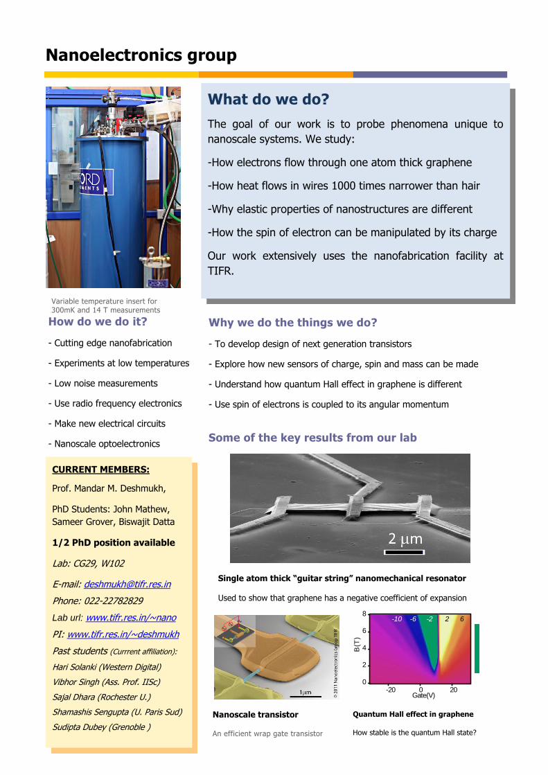
Variable temperature insert for 300mK and 14 T measurements
CURRENT MEMBERS:
Prof. Mandar M. Deshmukh,
PhD Students: John Mathew,
Sameer Grover, Biswajit Datta
1/2 PhD position available
Lab: CG29, W102
E-mail: [email protected]
Phone: 022-22782829
Lab url: www.tifr.res.in/~nano
PI: www.tifr.res.in/~deshmukh
Past students (Currrent affiliation):
Hari Solanki (Western Digital)
Vibhor Singh (Ass. Prof. IISc)
Sajal Dhara (Rochester U.)
Shamashis Sengupta (U. Paris Sud)
Sudipta Dubey (Grenoble )
Some of the key results from our lab
What do we do?
The goal of our work is to probe phenomena unique to
nanoscale systems. We study:
-How electrons flow through one atom thick graphene
-How heat flows in wires 1000 times narrower than hair
-Why elastic properties of nanostructures are different
-How the spin of electron can be manipulated by its charge
Our work extensively uses the nanofabrication facility at
TIFR.
Why we do the things we do?
- To develop design of next generation transistors
- Explore how new sensors of charge, spin and mass can be made
- Understand how quantum Hall effect in graphene is different
- Use spin of electrons is coupled to its angular momentum
How do we do it?
- Cutting edge nanofabrication
- Experiments at low temperatures
- Low noise measurements
- Use radio frequency electronics
- Make new electrical circuits
- Nanoscale optoelectronics
Nanoscale transistor
An efficient wrap gate transistor
Single atom thick “guitar string” nanomechanical resonator
Used to show that graphene has a negative coefficient of expansion
Quantum Hall effect in graphene
How stable is the quantum Hall state?
-20 0 20
8
6
4
2
0
Gate(V)
B(T
)
-2-6-10 2 6
Semiconductor Physics using Optical Spectroscopy
Cryogenic photo-luminescence spectroscopy setup (4.5 K, 1.5 m spatial resolution)
CURRENT MEMBERS:
PI: Prof. Sandip Ghosh
Vasam Sugunakar, Nihit Saigal
PhD positions available
Lab/Office: W139 / W137 E-mail: [email protected] Phone: 022-22782840 url: www.tifr.res.in/~sangho10/
Polarization resolved photoluminescence spectral images in
panel (b) & (c) of a single GaAs nanowire of mixed wurtzite-
zincblende phase, at 4.5K. The nanowire, seen in panel (a),
was grown in Paul Drude Institute, Berlin
What we do
Our research involves the study of electronic band structure of
semiconductor materials and physical properties that derive
from it. An understanding of such properties is crucial for
electronic and opto-electronic device applications. We employ a
variety of optical spectroscopy techniques and have studied
group III-V semiconductors such as GaN and GaAs families,
with emphasis on nanostructures such as Quantum Wells,
Wires and Dots. Our recent studies have been on the new class
of 2-dimensional mono-layer transition metal dichalcogenide
semiconductors such as MoS2.
Low dimensional semiconductor systems
Semiconductor materials can be grown in nanometer
dimensions with high crystalline quality using modern
epitaxial growth techniques. The small size can lead to
"quantum confinement" of electrons and holes resulting in
fewer accessible energy states, unlike continuous energy
bands in a 3-dimensional (3D) solid. Such structures can
be categorized as super-lattices, quantum
wells/wires/dots depending on the number of dimensions
in which the carriers are confined. Transition metal
dichalcogenides such as MoS2, which can exist as stable
mono-layers, represents another type low dimensional
(2D) system.
Tools & Techniques
We use spectroscopic techniques such as absorption, reflection,
Raman, photo/electro luminescence, photo-voltage/current and
modulation techniques such as electro-reflectance, ellipsometry and
magneto-optic-Kerr-effect spectroscopy. The setups we have built
consist of monochromators, light sources including lasers, detectors,
specialized optical components and measurement electronics.
Measurements can be done in the wavelength range of 250nm -
14000nm covering the UV-VIS-NIR-MIR-FIRrange. The sample
temperature can be varied in the range 4.5K - 400K in magnetic
fields up to 7T, with high spatial resolution down to ~1.5m.
Quantum confinement can lead to dramatic changes in material properties. For instance the bandgap, a fundamental
property of a semiconductor, can change. Sometimes structural changes in nano-materials can lead to interesting
effects such as strongly polarized emission from the wurtzite phase of GaAs which form when GaAs is grown in the
form a nano-wire (see adjacent figure). Understanding such properties is essential for designing semiconductor
devices, especially opto-electronic devices such as lasers and light emitting diodes, with significantly improved
characteristics. We use optical spectroscopy to study such electronic band structure changes where we glean
information from not just the photon energy, but also from the material’s sensitivity to the polarization state of light.
CURRENT MEMBERS: Kalobaran Maiti, Khadiza Ali, Tanusree Saha, and K. Srinivas
Lab: BG37 url: www.tifr.res.in/~peslab/ PhD positions available
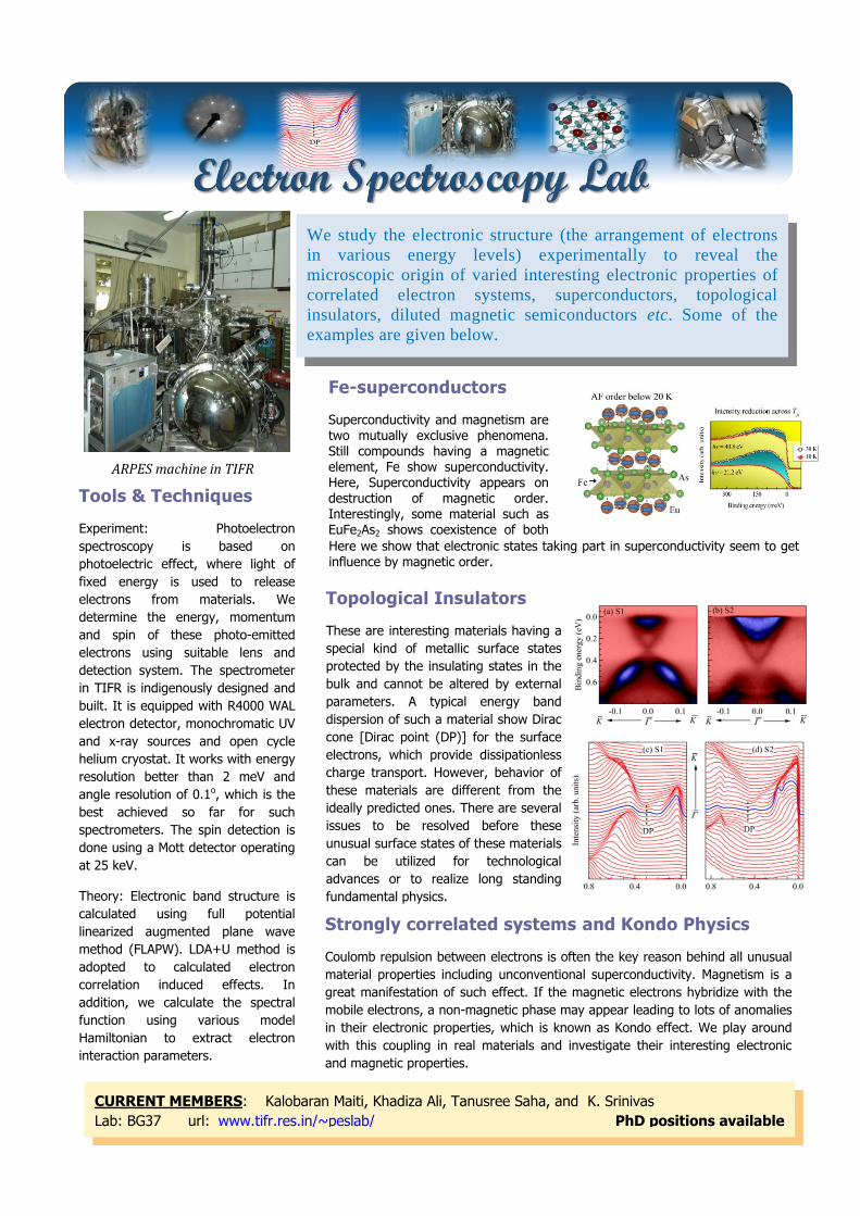
Topological Insulators
These are interesting materials having a
special kind of metallic surface states
protected by the insulating states in the
bulk and cannot be altered by external
parameters. A typical energy band
dispersion of such a material show Dirac
cone [Dirac point (DP)] for the surface
electrons, which provide dissipationless
charge transport. However, behavior of
these materials are different from the
ideally predicted ones. There are several
issues to be resolved before these
unusual surface states of these materials
can be utilized for technological
advances or to realize long standing
fundamental physics.
We study the electronic structure (the arrangement of electrons
in various energy levels) experimentally to reveal the
microscopic origin of varied interesting electronic properties of
correlated electron systems, superconductors, topological
insulators, diluted magnetic semiconductors etc. Some of the
examples are given below.
Tools & Techniques
Experiment: Photoelectron
spectroscopy is based on
photoelectric effect, where light of
fixed energy is used to release
electrons from materials. We
determine the energy, momentum
and spin of these photo-emitted
electrons using suitable lens and
detection system. The spectrometer
in TIFR is indigenously designed and
built. It is equipped with R4000 WAL
electron detector, monochromatic UV
and x-ray sources and open cycle
helium cryostat. It works with energy
resolution better than 2 meV and
angle resolution of 0.1o, which is the
best achieved so far for such
spectrometers. The spin detection is
done using a Mott detector operating
at 25 keV.
Theory: Electronic band structure is
calculated using full potential
linearized augmented plane wave
method (FLAPW). LDA+U method is
adopted to calculated electron
correlation induced effects. In
addition, we calculate the spectral
function using various model
Hamiltonian to extract electron
interaction parameters.
ARPES machine in TIFR
Here we show that electronic states taking part in superconductivity seem to get influence by magnetic order.
Strongly correlated systems and Kondo Physics
Coulomb repulsion between electrons is often the key reason behind all unusual
material properties including unconventional superconductivity. Magnetism is a
great manifestation of such effect. If the magnetic electrons hybridize with the
mobile electrons, a non-magnetic phase may appear leading to lots of anomalies
in their electronic properties, which is known as Kondo effect. We play around
with this coupling in real materials and investigate their interesting electronic
and magnetic properties.
Fe-superconductors
Superconductivity and magnetism are two mutually exclusive phenomena. Still compounds having a magnetic element, Fe show superconductivity. Here, Superconductivity appears on destruction of magnetic order. Interestingly, some material such as EuFe2As2 shows coexistence of both the phenomena.

Fundamental Optics, THz & Optical Nanostructures
Two home built THz setups for
performing transmission (box
enclosed) and reflection THz.
spectroscopy
CURRENT MEMBERS:
Dr. S. S. Prabhu, Gajendra
Mulay, Abhishek Singh, Harshad
Surdi, Dr. Bagvanth Reddy
Sangala (Post-Doc)
PhD positions available
Lab: C225
E-mail: [email protected]
Phone: 022-22782933
url: www.tifr.res.in/~Foton/
Applications
Some of the exotic materials or molecules have very interesting
properties which are related in turn to the way charge carriers are
arranged or the way they respond to external stimulation. THz
spectroscopy can tell a lot about conductivity response of such carriers.
We can record the amplitude of the THz light field, how it oscillates in
femtosecond (10-15 sec) time scale. When passing through the sample it
changes appropriately revealing all the information. We are interested in
studying this information and improve our understanding.
Welcome to Foton Lab: THz Activity
In Ultrafast Optics and Tera-Hertz (THz) Spectroscopy
activity, Foton lab at TIFR primarily investigates ultra-fast
phenomena, carrier dynamics and various optical
phenomena involving THz radiation. Several biological and
chemical molecules have vibrational frequency lines falling
in the THz regime. Several materials exhibit exotic
properties which are due to their rearrangement of charge
carriers. These properties change with temperature, electric
field or magnetic field or under optical fluence. THz
radiation measures conductivity these carriers. Our lab aims
to tackle the basic challenges to understand these
processes with homebuilt sources, detectors and setups.
THz Spectroscopy (1012Hz)
The THz radiation has wavelengths from 30 microns (10THz) to 1000
microns (0.3THz) as opposed to visible (0.4 to 0.7 microns). This is the
final frontier in electro-magnetic spectrum which needs to be explored in
terms of high power sources, sensitive detectors and spectroscopy
setups. One of the central challenges in building such a system is, high
intensity sources or detectors are not available. We don’t yet know how
to make them! So we try various designs for increasing the THz emission
and detection efficiency. This requires study of several different types of
materials and charge carrier dynamics in them is possibly the key for
solving this problem. The spectroscopy has several applications from
medicine to condensed matter physics and the field is wide open.
Tools & Techniques
Our experiments are carried out
at temperatures varying from
320K up to 10K, achieved using a
closed cycle helium refrigerator.
The THz (antenna) sources and
detectors are made out of
Gallium Arsenide (GaAs) wafers
using conventional photo- or
nano-lithography in a cleanroom.
We use ultra-short pulsed laser
(10fs, 800nm, 80MHz) for
exciting carriers in GaAs to
generate THz signal. The
generated THz pulse (~1ps
duration) is used to study our
samples. We also fabricate
necessary components for THz
optics which are not available.
India’s First THz Image of Father of our nation which we have taken in our lab in TIFR from 500Rs currency watermark.
0 5 10
-20
-10
0
10
20
Sig
na
l (a
.u.)
Delay (ps)
A Typical THz Pulse waveform recorded in our laboratory. The entire pulse
duration is in few picoseconds.

Superconductivity and low Temperature Scanning Tunneling Spectroscopy Laboratory
(top) Atomic resolution STM image of NbSe2 single crystal showing the atoms and the charge density wave modulation. (bottom) Image of the vortex lattice at 350 mK and 0.2T in the same sample obtained using the spectroscopic imaging mode.
CURRENT MEMBERS:
PI: Prof. Pratap Raychaudhuri
Somesh Chandra Ganguli, Rini
Ganguly, Indranil Roy, Dibyendu Bala,
Harkirat Singh (post-doc), Vivas
Bagwe, John Jesudasan
PhD positions available
Lab: CG24 / CG30
E-mail: [email protected]
Phone: 022-22782201
url: www.tifr.res.in/~superconductivity
Schematic view of the 350 mK scanning tunneling microscope at TIFR.
Welcome to Superconductivity lab
The Superconductivity lab in TIFR is primarily involved with
the study of novel ground states that emerge as a result of
interaction and disorder in conventional and unconventional
superconductors. Our main workhorse, are two state-of-the-
art home built scanning tunneling microscopes (STM),
operating down to 300 mK and in magnetic fields up to 9T.
We complement STM measurements with transport and
magnetic measurements in different frequency domains,
ranging from dc all the way to microwave. We also use
these techniques to look at systems other than
superconductors, such as charge density waves and
magnetic systems. (more details on website)
Scanning tunneling spectroscopy
The scanning tunneling microscope (STM) relies on quantum mechanical
tunneling of electrons from the surface of the sample to an atomically
sharp tip, to obtain an atomically resolved image of the surface. However,
the greatest advantage of an STM stems from its ability to simultaneously
capture spectroscopic information through the measurement of tunneling
conductance, with atomic spatial resolution and unsurpassed energy
resolution (<100 eV). This makes STM particularly suited to study
correlated electron systems, including superconductors where exotic
electronic states emerge from subtle redistribution of electrons within few
meV around the Fermi energy. The TIFR STMs combine, in-situ thin films
growth and surface preparation capability, such that measurements can
be performed on pristine surfaces, uncontaminated from exposure to air.
Tools & Techniques
Our experiments are carried out at
cryogenic temperatures of down to
300 mK, achieved using several of 3He cryostat specially adapted for
specific experiments. Our materials
for investigation consist of either
thin films or single crystals. High
quality epitaxial thin films of
superconducting and other
materials are grown using a
variety of techniques including,
magnetron sputtering, pulsed laser
deposition and thermal
evaporation and characterized
using tools such as XRD, SEM,
EPMA before measurements.

Correlated Electron Systems: Oxides/Intermetallics
Structure of a low dimensional oxide system studied extensively by us, Ca3Co2O6
FACULTY MEMBERS:
Prof. E.V. Sampathkumaran and
Prof. P.L. Paulose
Labs: AB94B and CG28
E-mail: [email protected]
Phone: 022-22782437/2412
Highlights
The f-electron anomalies in bulk form:
Evidence for the validity of spin-density-wave picture (as against 'local-moment' picture)
as quantum critical-point is approached - a major issue in the field of 'heavy-fermions',
(PRB 82, 104428 (2010)). Anomalous magnetic ordering in a Nd-based intermetallic
compound, emphasizing the need to explore strong electron correlation effects in Nd
systems (PRB 84, 184415 (2011)).
Huge enhancement of magnetoresistance, with a positive sign which is unexpected at the
metamagnetic transition; possible ‘Inverse metamagnetism’, an interesting new concept
(e.g., PRB 79, 060403(R) (2009); PRB 80, 214425 (2009); PRB 81, 184434 (2010)).
Particle-size effects in intermetalics:
First demonstration of particle-size induced ferromagnetism in an exchange-enhanced
"Pauli paramagnet" like YCo2. Interestingly, f-electron electron localization leading to
magnetic ordering has been reported even for (non-magnetic) Kondo lattice. (APL 92,
192506 (2008); PRB 80, 024401 (2009)).
Spin-chain magnetism:
Identification of anisotropic spin-glass anomalies and spin-chain magnetism (Tb2PdSi3),
unusual among among intermetallics (PRB 67, 212401 (2003)).
Magnetoelectric coupling and multiferroicity in a Haldane spin-chain system (PRB 88,
094438 (2013)).
In Ca3Co2O6 and its derivatives, we reported evidence for hitherto unrealized 'incipient'
spin-chain ordering at a temperature much higher than Néel temperature, coupled with
phonon and magnon anomalies! A rare phenomenon of "spin-chain-induced
multiferroicity", that too, above 77 K, was discovered bearing relevance to applications
(PRB 77, 172403 (2008); 79, 094103 (2009); JAP 108, 103517 (2010); (Nature Group)
Sci. Rep. 3, 3104 (2013).
Welcome to our lab
Competing interactions plays a crucial role in controlling the
physical properties of materials, making this field of research
lively. In our laboratories, apart from focussing on discovering
novel materials, we investigate how various phenomena of great
current interest compete by changing temperature, external and
chemical pressure, magnetic fields and particle size. Some of the
topics of current interest are: (i) Competition between magnetic
ordering and the Kondo effect (in the field of "Heavy fermions"),
which favours non-magnetism; (iii) Competition between
magnetism and ferroelectricity ("multiferrocity”); (iii) What
happens to the spins arranged in a triangular fashion which are
coupled antiparallel to each other (leading to what is known as
"geometrically frustrated magnetism")? A comparison of the
properties of materials in bulk and single-crystalline forms with
those of nanocrystals has been found to be valuable to
understand some of the issues in the field. Apart from these,
topics relevant to applications like magneto-caloric effect are also
being undertaken.
Tools & Techniques
We have facilities to synthesize
the materials in bulk form, single
crystal and nanoform. Many
experimental facilities down to
subhelium temperatures and high
magnetic fields exist in our labo-
ratories - heat-capacity, magneti-
zation, electrical resistivity therm-
opower, complex dielectric prop-
erties and electric polarization
and Mössbauer spectroscopy. In
addition we collaborate with
other labs for studies like neutron
diffraction, Raman and Photoele-
ctron spectroscopy. Several dep-
artment facilities like TEM, SEM,
XRD are available for charact-
erizing the materials. We also
specialize in performing electrical
resistivity and magnetization
under high pressure.

Crystal Growth Laboratory
Tetra-arc furnace to grow single crystals by Czochralski method
CURRENT MEMBERS:
Prof. S. K. Dhar and
Prof. A. Thamizhavel; Ms. Ruta
Kulkarni, Mr. Arvind Maurya,
Dr. Arvind yogi and Dr. Md.
Matin
PhD positions available
Lab: AB-81
E-mail: [email protected]
Phone: 022-22782438
url: www.tifr.res.in/~crystalgrowth/
Czochralski crystal growth in a tetra-arc furnace.
Anisotropic magnetization in CeGe single crystal. The [010] direction represents the easy axis of magnetization
Quantum Phase Transition
The magnetic phase transition occurring at finite temperature of the
SCES of mainly cerium or ytterbium compounds can be continuously
tuned from a magnetically ordered state to a non-magnetic ground
state by a non-thermal external control parameters such as high
pressure, composition or magnetic field. For a critical value of the
control parameter, the magnetic phase transition approaches a T = 0
phase transition or the so called quantum phase transition (QPT) which
separates a magnetically ordered from a non-magnetic ground state at
zero temperature. One of the objectives of this laboratory is to look for
such materials that exhibit QPT.
Welcome to Crystal Growth lab
The main theme of the crystal growth lab is to grow the
single crystals and study the anisotorpic physical properties
of strongly correlated electron systems (SCES). The single
crystals are grown by employing different crystal growth
techniques like Czochralski method, Bridgman method, high
temperature solution growth and vapor transport methods.
The grown crystals are oriented along the crystallographic
directions by means of Laue diffraction and cut along the
crystallographic directions by means of spark erosion cutting
machine for the anisotropic physical property
measurements.
Strongly correlated electron system (SCES)
In some of the intermetallic compounds, the conduction electrons interact
very strongly with the magnetic atoms present in the system and hence
the magnetic ordering of the magnetic atoms is suppressed and the
magnetic character of the atoms is dragged along or hybridized with the
conduction electrons. Such types of systems are classified as SCES. The
competition between the long range magnetic order and the itinerancy of
the electrons on the magnetic atoms leads to diverse ground states. Ce
and Yb-based intermetallic compounds are studied quite extensively by
growing the single crystals of these compounds.
Tools & Techniques
Single crystals are grown using a
variety of methods. A tetra-arc
furnace and an optical floating
zone furnace are the main work
horses to grow single crystals by
Czochrlaski and floating zone
methods apart from the usual
box type furnaces to grow single
crystals by flux method. A Laue
diffractometer to orient the single
crystals. A physical property
measurement systems (PPMS)
with a 14-T magnet to measure
specific heat capacity and
electrical resistivity down to 50
mK using the dilution insert.

A dilution refrigerator capable of
cooling to a temperature of 10 mK
CURRENT MEMBERS:
PI: Dr. R. Vijayaraghavan
Dr. Madhavi Chand, Tanay Roy,
Suman Kundu, Sumeru Hazra,
Arpit Ranadive, Naveen Nehra,
Meghan Patankar
PhD positions available
Lab: W105 / W106
E-mail: [email protected]
Phone: 022-22782477
url: www.tifr.res.in/~quantro/
Top: Scanning Electron Microscope image of a superconducting qubit. Right: Impedance engineered parametric amplifier and its gain and noise data. Our new designed allowed nearly a 10X performance
improvement (arXiv:1510.03065)
Quantum Simulations
The computational resources required to simulate quantum mechanics on
a classical computer grows exponentially with the size of the simulated
system. Feynman had originally suggested that one should use quantum
systems to simulate quantum mechanics. The basic idea is to have a well
characterized and controllable quantum system to mimic the behaviour of
other systems of interest. Our lab is interested in studying collective
behaviour in superconducting qubits and developing the necessary
architecture for performing quantum simulations.
Welcome to QuMaC lab
The Quantum Measurement and Control Laboratory
(QuMaC) at TIFR primarily investigates quantum
phenomena in superconducting circuits. These
nanofabricated electrical circuits are engineered to behave
as “artificial atoms” with quantized energy levels. Two of
those levels can form a quantum bit (qubit) and used to
store and process information. With such qubits, one can
build powerful computing machines capable of providing
exponential speed up for certain mathematical problems.
Our lab aims to tackle the basic challenges in building and
controlling such quantum systems.
Quantum Feedback Control
One of the central challenges in building a quantum computer is that the
qubits do not maintain their quantum nature for a very long time. This
phenomena is called decoherence and happens primarily due to
environmental noise. However, it is possible to use multiple imperfect
qubits to build a near-perfect qubit using a process called quantum error
correction. This involves encoding the single qubit state among multiple
physical qubits, making the right kind of measurements to detect any
errors and then use feedback to correct those errors. We are investigating
techniques to implement quantum error correction using weak continuous
measurements and feedback. This will involve ultra-fast signal processing
using Field Programmable Gate Arrays (FPGA).
Tools & Techniques
Our experiments are carried out
at cryogenic temperatures of
around 10 mK, achieved using a
dilution refrigerator. The
superconducting circuits are
made out of aluminium on silicon
or sapphire wafers using nano-
lithography in a cleanroom. We
use microwave frequency (4 – 8
GHz) signals to manipulate and
measure our devices. We use
high speed digitizers and FPGAs
to record and process the
measurement signals at GHz
rates. We also design and build
custom microwave frequency
amplifiers, filters, attenuators and
circuit boards.
Quantum Measurement and Control Laboratory
1 m 1 cm