DEPARTMENT OF COMPUTER SCIENCE AND ENGINEERING LAB MANUAL ... · PDF file lab manual/cse i ....
48
<CS0413/VLSI> Lab Manual/CSE i DEPARTMENT OF COMPUTER SCIENCE AND ENGINEERING LAB MANUAL Academic Year: 2015-16 ODD SEMESTER Programme (UG/PG) : UG Semester : VII Course Code : CS0413 Course Title : VLSI LAB Prepared By <K.SATHIYAPRIYA> (<AP>, Department of Computer Science and Engineering) FACULTY OF ENGINEERING AND TECHNOLOGY SRM UNIVERSITY (Under section 3 of UGC Act, 1956) SRM Nagar, Kattankulathur- 603203 Kancheepuram District
Transcript of DEPARTMENT OF COMPUTER SCIENCE AND ENGINEERING LAB MANUAL ... · PDF file lab manual/cse i ....
<CS0413/VLSI> Lab Manual/CSE i
DEPARTMENT OF COMPUTER SCIENCE AND ENGINEERING
LAB MANUAL
Academic Year: 2015-16 ODD SEMESTER
Programme (UG/PG) : UG
Semester : VII
Course Code : CS0413
Course Title : VLSI LAB
Prepared By
<K.SATHIYAPRIYA> (<AP>, Department of Computer Science and Engineering)
FACULTY OF ENGINEERING AND TECHNOLOGY SRM UNIVERSITY
(Under section 3 of UGC Act, 1956)
SRM Nagar, Kattankulathur- 603203 Kancheepuram District
<CS0413/VLSI> Lab Manual/CSE
ii
LIST OF EXPERIMENTS & SCHEDULE
Course Code: CS0413 Course Title: VLSI AND EMBEDDED SYSTEM DESIGN LAB
Exp. No. Title Week No.
S. No Experiments Page. No
1 Design of Logic gates 1
2 Design of Binary Adders 2
3 Design of Multiplexers and De-multiplexers 3
4 Design of Encoders and Decoders 4
5 Flip Flops 5
6 Counters 6
7 Bitwise Operators Using 8051 7
8 Toggle a Port bit in 8051 8
9 Delay Operators in 8051 9
Course Coordinator HOD
<CS0413/VLSI> Lab Manual/CSE
iii
Internal Assessment Mark Split Up
Observation : 20 Marks Attendance : 5 Marks Mini Project with the Report (Max. 8 Pages & 3 Students per Batch) : 20 Marks Model Exam : 15 Marks TOTAL MARKS : 60 Marks

<CS0413/VLSI> Lab Manual/CSE
1
Introduction to Combinational Circuit Design
EXP:1 Design of Logic gates 1.1 Introduction The purpose of this experiment is to simulate the behavior of several of the basic logic gates and you will
connect several logic gates together to create simple digital model.
1.2 Software tools Requirement Equipments:
Computer with Modelsim Software
Specifications:
HP Computer P4 Processor – 2.8 GHz, 2GB RAM, 160 GB Hard Disk
Softwares: Modelsim - 5.7c, Xilinx - 6.1i.
Algorithm
STEP 1: Open ModelSim XE II / Starter 5.7C
STEP 2: File -> Change directory -> D:\<register number>
STEP 3: File -> New Library -> ok
STEP 4: File -> New Source -> Verilog
STEP 5: Type the program
STEP 6: File -> Save -> <filename.v>
STEP 7: Compile the program
STEP 8: Simulate -> expand work -> select file -> ok
STEP 9: View -> Signals
STEP 10: Select values -> Edit -> Force -> input values
STEP 11: Add -> Wave -> Selected signals -> Run
STEP 12: Change input values and run again
<CS0413/VLSI> Lab Manual/CSE
2
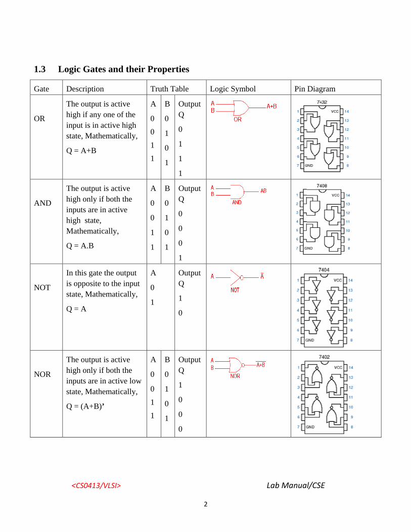
1.3 Logic Gates and their Properties
Gate Description Truth Table Logic Symbol Pin Diagram
OR
The output is active high if any one of the input is in active high state, Mathematically,
Q = A+B
A
0 0 1 1
B
0
1
0
1
Output Q
0
1
1
1
AND
The output is active high only if both the inputs are in active high state, Mathematically,
Q = A.B
A
0
0
1
1
B
0
1
0
1
Output Q
0
0
0
1
NOT
In this gate the output is opposite to the input state, Mathematically,
Q = A
A
0
1
Output Q
1
0
NOR
The output is active high only if both the inputs are in active low state, Mathematically,
Q = (A+B)’
A
0
0 1 1
B
0
1
0
1
Output Q
1
0
0
0
<CS0413/VLSI> Lab Manual/CSE
3
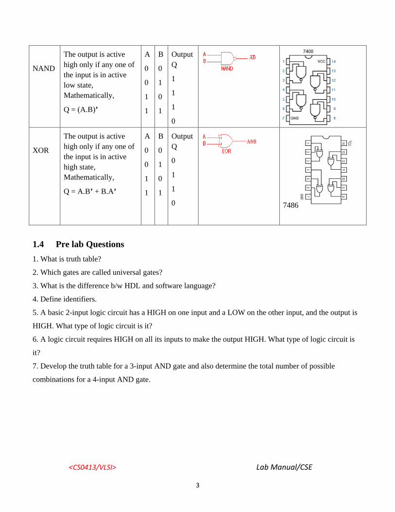
NAND
The output is active high only if any one of the input is in active low state, Mathematically,
Q = (A.B)’
A
0
0
1
1
B
0
1
0
1
Output Q
1
1
1
0
XOR
The output is active high only if any one of the input is in active high state, Mathematically,
Q = A.B’ + B.A’
A
0
0
1
1
B
0
1
0
1
Output Q
0
1
1
0
7486
1.4 Pre lab Questions 1. What is truth table?
2. Which gates are called universal gates?
3. What is the difference b/w HDL and software language?
4. Define identifiers.
5. A basic 2-input logic circuit has a HIGH on one input and a LOW on the other input, and the output is
HIGH. What type of logic circuit is it?
6. A logic circuit requires HIGH on all its inputs to make the output HIGH. What type of logic circuit is
it?
7. Develop the truth table for a 3-input AND gate and also determine the total number of possible
combinations for a 4-input AND gate.
<CS0413/VLSI> Lab Manual/CSE
4
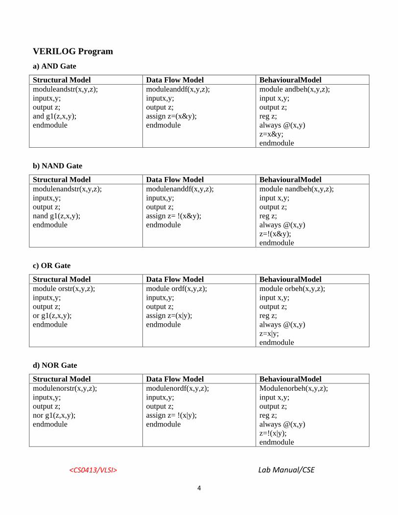
VERILOG Program
a) AND Gate
Structural Model Data Flow Model BehaviouralModel moduleandstr(x,y,z); inputx,y; output z; and g1(z,x,y); endmodule
moduleanddf(x,y,z); inputx,y; output z; assign z=(x&y); endmodule
module andbeh(x,y,z); input x,y; output z; reg z; always @(x,y) z=x&y; endmodule
b) NAND Gate
Structural Model Data Flow Model BehaviouralModel modulenandstr(x,y,z); inputx,y; output z; nand g1(z,x,y); endmodule
modulenanddf(x,y,z); inputx,y; output z; assign z= !(x&y); endmodule
module nandbeh(x,y,z); input x,y; output z; reg z; always @(x,y) z=!(x&y); endmodule
c) OR Gate
Structural Model Data Flow Model BehaviouralModel module orstr(x,y,z); inputx,y; output z; or g1(z,x,y); endmodule
module ordf(x,y,z); inputx,y; output z; assign z=(x|y); endmodule
module orbeh(x,y,z); input x,y; output z; reg z; always @(x,y) z=x|y; endmodule
d) NOR Gate
Structural Model Data Flow Model BehaviouralModel modulenorstr(x,y,z); inputx,y; output z; nor g1(z,x,y); endmodule
modulenordf(x,y,z); inputx,y; output z; assign z= !(x|y); endmodule
Modulenorbeh(x,y,z); input x,y; output z; reg z; always @(x,y) z=!(x|y); endmodule
<CS0413/VLSI> Lab Manual/CSE
5
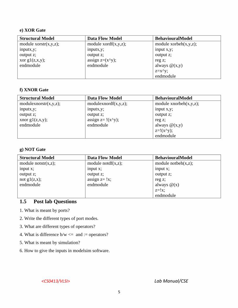
e) XOR Gate
Structural Model Data Flow Model BehaviouralModel module xorstr(x,y,z); inputx,y; output z; xor g1(z,x,y); endmodule
module xordf(x,y,z); inputx,y; output z; assign z=(x^y); endmodule
module xorbeh(x,y,z); input x,y; output z; reg z; always @(x,y) z=x^y; endmodule
f) XNOR Gate
Structural Model Data Flow Model BehaviouralModel modulexnorstr(x,y,z); inputx,y; output z; xnor g1(z,x,y); endmodule
modulexnordf(x,y,z); inputx,y; output z; assign z= !(x^y); endmodule
module xnorbeh(x,y,z); input x,y; output z; reg z; always @(x,y) z=!(x^y); endmodule
g) NOT Gate
Structural Model Data Flow Model BehaviouralModel module notstr(x,z); input x; output z; not g1(z,x); endmodule
module notdf(x,z); input x; output z; assign z= !x; endmodule
module notbeh(x,z); input x; output z; reg z; always @(x) z=!x; endmodule
1.5 Post lab Questions 1. What is meant by ports?
2. Write the different types of port modes.
3. What are different types of operators?
4. What is difference b/w <= and := operators?
5. What is meant by simulation?
6. How to give the inputs in modelsim software.
<CS0413/VLSI> Lab Manual/CSE
6
1.6 Lab Report Each individual will be required to submit a lab report. Use the format specified in the "Lab
Report Requirements” document available on the class web page. Be sure to include the following items
in your lab report:
Lab cover sheet with staff verification sign.
Answer the pre-lab questions
Complete VERILOG code design for all logic gates and output signal waveforms
Answer the post-lab questions
1.6 Grading Pre-lab Work 20 points
Lab Performance 30 points
Post-lab Work 20 points
Lab report 30 points
For the lab performance - at a minimum, demonstrate the operation of all the logic gates to your staff in-
charge:
The lab report will be graded as follows (for the 30 points):
VERILOG code for each logic gates 15 points
Output signal waveform for all logic gates and its truth table 15 points
<CS0413/VLSI> Lab Manual/CSE
7
EXP:2 Design of Binary Adders
2.1 Introduction The purpose of this experiment is to introduce the design of simple combinational circuits, in this case
half adders, half subtractors, full adders and full subtractors.
Software tools Requirement
Equipments:
Computer with Modelsim Software
Specifications:
HP Computer P4 Processor – 2.8 GHz, 2GB RAM, 160 GB Hard Disk
Softwares: Modelsim - 5.7c, Xilinx - 6.1i.
Algorithm
STEP 1: Open ModelSim XE II / Starter 5.7C
STEP 2: File -> Change directory -> D:\<register number>
STEP 3: File -> New Library -> ok
STEP 4: File -> New Source -> Verilog
STEP 5: Type the program
STEP 6: File -> Save -> <filename.v>
STEP 7: Compile the program
STEP 8: Simulate -> expand work -> select file -> ok
STEP 9: View -> Signals
STEP 10: Select values -> Edit -> Force -> input values
STEP 11: Add -> Wave -> Selected signals -> Run
STEP 12: Change input values and run again
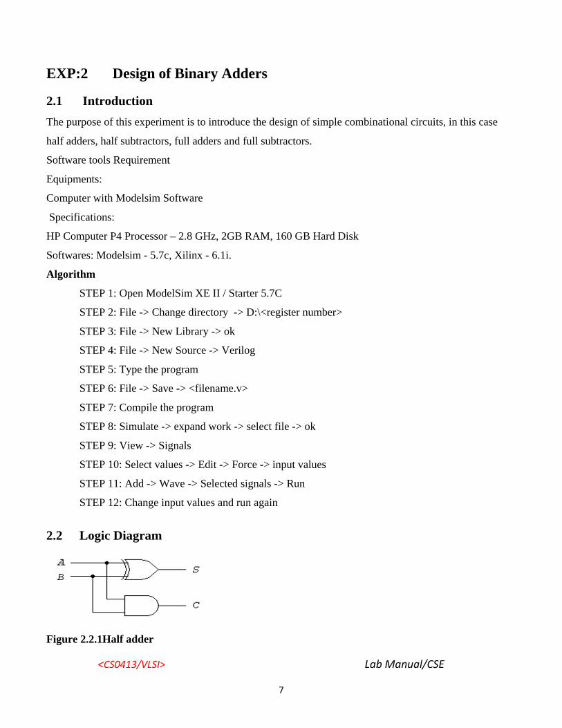
2.2 Logic Diagram
Figure 2.2.1Half adder

<CS0413/VLSI> Lab Manual/CSE
8
Figure 2.2.2 Full adder
Figure 2.2.3Halfsubtractor
Figure 2.2.4 Full subtractor
2.3 Pre lab Questions
1. What is meant by combinational circuits?
2. Write the sum and carry expression for half and full adder.
3. Write the difference and borrow expression for half and full subtractor.
4. What is signal? How it is declared?
<CS0413/VLSI> Lab Manual/CSE
9
VERILOG Program
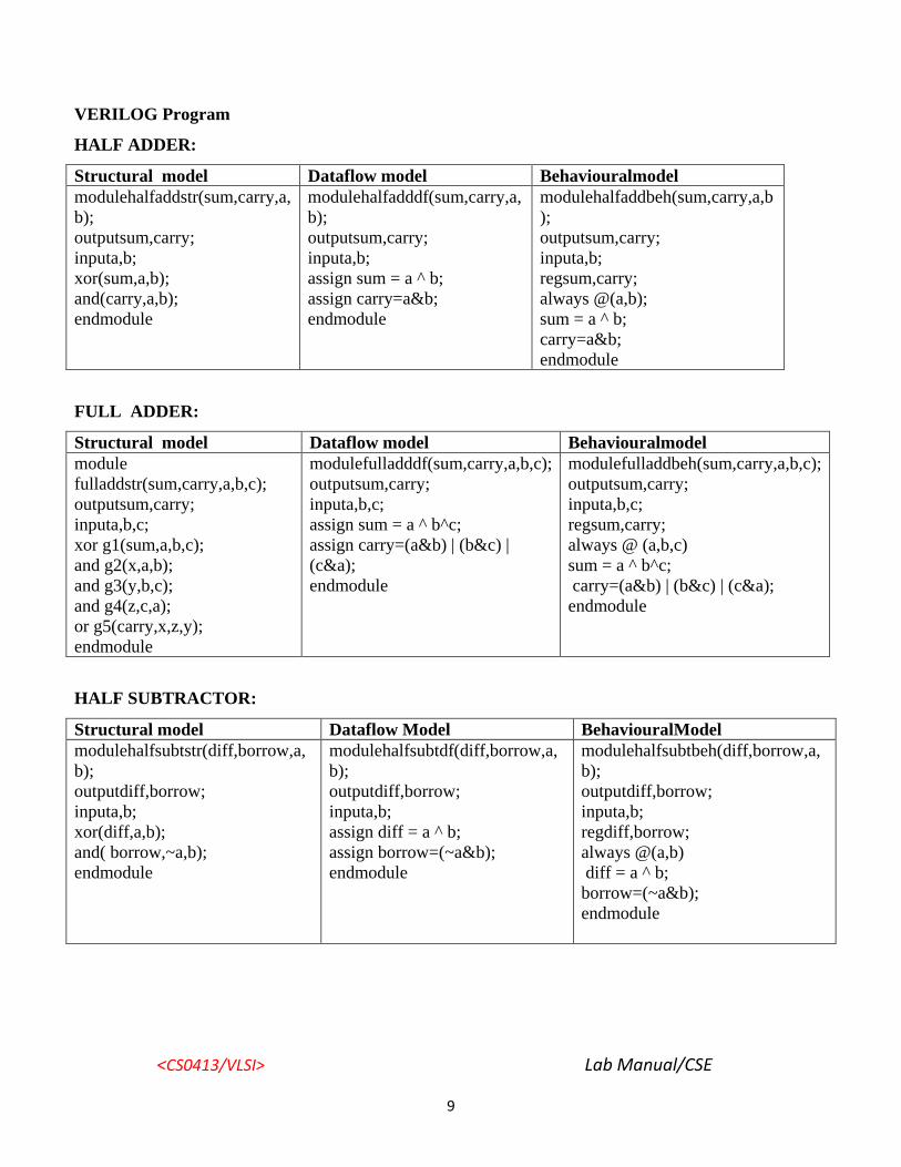
HALF ADDER:
Structural model Dataflow model Behaviouralmodel modulehalfaddstr(sum,carry,a,b); outputsum,carry; inputa,b; xor(sum,a,b); and(carry,a,b); endmodule
modulehalfadddf(sum,carry,a,b); outputsum,carry; inputa,b; assign sum = a ^ b; assign carry=a&b; endmodule
modulehalfaddbeh(sum,carry,a,b); outputsum,carry; inputa,b; regsum,carry; always @(a,b); sum = a ^ b; carry=a&b; endmodule
FULL ADDER:
Structural model Dataflow model Behaviouralmodel module fulladdstr(sum,carry,a,b,c); outputsum,carry; inputa,b,c; xor g1(sum,a,b,c); and g2(x,a,b); and g3(y,b,c); and g4(z,c,a); or g5(carry,x,z,y); endmodule
modulefulladddf(sum,carry,a,b,c); outputsum,carry; inputa,b,c; assign sum = a ^ b^c; assign carry=(a&b) | (b&c) | (c&a); endmodule
modulefulladdbeh(sum,carry,a,b,c); outputsum,carry; inputa,b,c; regsum,carry; always @ (a,b,c) sum = a ^ b^c; carry=(a&b) | (b&c) | (c&a); endmodule
HALF SUBTRACTOR:
Structural model Dataflow Model BehaviouralModel modulehalfsubtstr(diff,borrow,a,b); outputdiff,borrow; inputa,b; xor(diff,a,b); and( borrow,~a,b); endmodule
modulehalfsubtdf(diff,borrow,a,b); outputdiff,borrow; inputa,b; assign diff = a ^ b; assign borrow=(~a&b); endmodule
modulehalfsubtbeh(diff,borrow,a,b); outputdiff,borrow; inputa,b; regdiff,borrow; always @(a,b) diff = a ^ b; borrow=(~a&b); endmodule
<CS0413/VLSI> Lab Manual/CSE
10
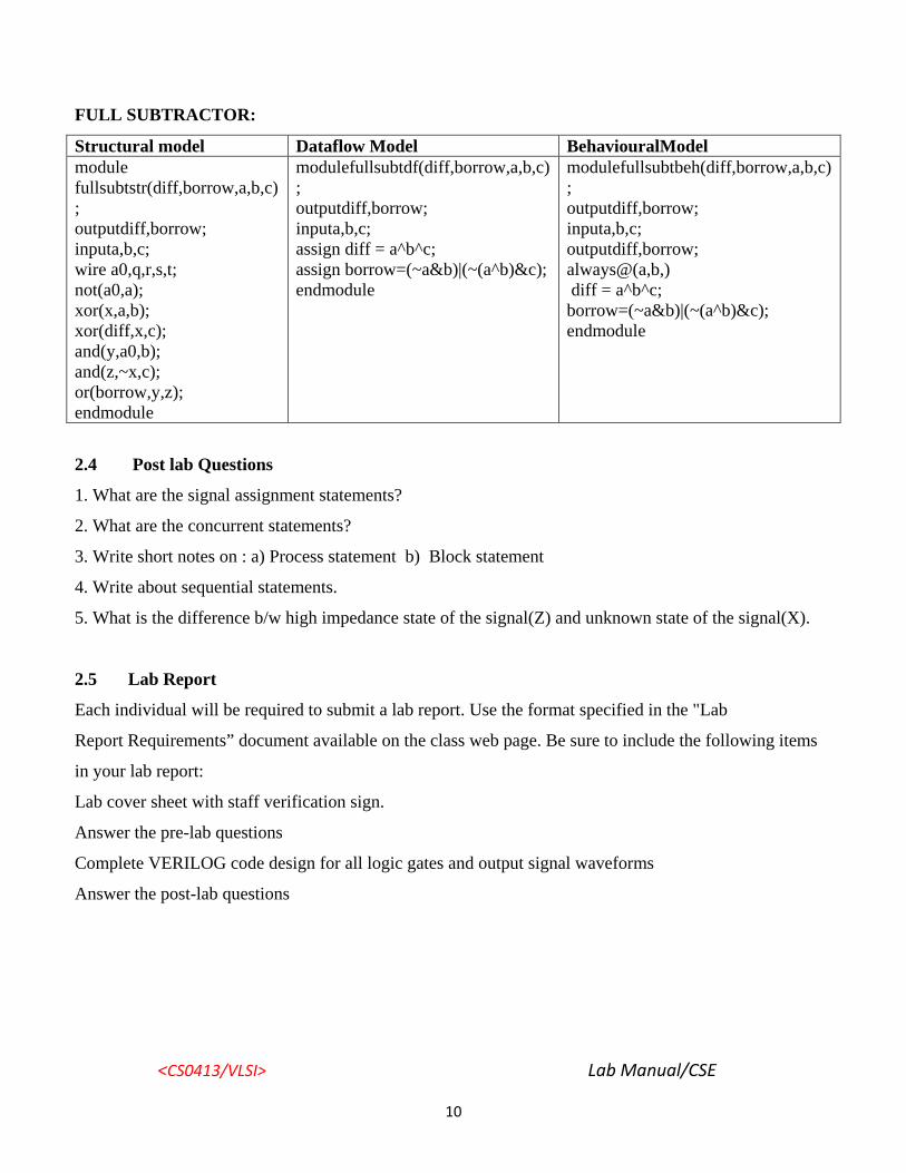
FULL SUBTRACTOR:
Structural model Dataflow Model BehaviouralModel module fullsubtstr(diff,borrow,a,b,c); outputdiff,borrow; inputa,b,c; wire a0,q,r,s,t; not(a0,a); xor(x,a,b); xor(diff,x,c); and(y,a0,b); and(z,~x,c); or(borrow,y,z); endmodule
modulefullsubtdf(diff,borrow,a,b,c); outputdiff,borrow; inputa,b,c; assign diff = a^b^c; assign borrow=(~a&b)|(~(a^b)&c); endmodule
modulefullsubtbeh(diff,borrow,a,b,c); outputdiff,borrow; inputa,b,c; outputdiff,borrow; always@(a,b,) diff = a^b^c; borrow=(~a&b)|(~(a^b)&c); endmodule
2.4 Post lab Questions
1. What are the signal assignment statements?
2. What are the concurrent statements?
3. Write short notes on : a) Process statement b) Block statement
4. Write about sequential statements.
5. What is the difference b/w high impedance state of the signal(Z) and unknown state of the signal(X).
2.5 Lab Report
Each individual will be required to submit a lab report. Use the format specified in the "Lab
Report Requirements” document available on the class web page. Be sure to include the following items
in your lab report:
Lab cover sheet with staff verification sign.
Answer the pre-lab questions
Complete VERILOG code design for all logic gates and output signal waveforms
Answer the post-lab questions

<CS0413/VLSI> Lab Manual/CSE
11
2.6 Grading
Pre-lab Work 20 points
Lab Performance 30 points
Post-lab Work 20 points
Lab report 30 points
For the lab performance - at a minimum, demonstrate the operation of all the logic gates to your staff in-
charge
The lab report will be graded as follows (for the 30 points):
VERILOG code for each experiments 15 points
Output signal waveform for all experiments and its truth table 15 points
<CS0413/VLSI> Lab Manual/CSE
12
EXP:3 Design of Multiplexers and Demultiplexers
3.1 Introduction The purpose of this experiment is to write and simulate a VERILOG program for Multiplexers and
Demultiplexers.
Software tools Requirement: Equipments:
Computer with Modelsim Software
Specifications:
HP Computer P4 Processor – 2.8 GHz, 2GB RAM, 160 GB Hard Disk
Softwares: Modelsim - 5.7c, Xilinx - 6.1i.
Algorithm
STEP 1: Open ModelSim XE II / Starter 5.7C
STEP 2: File -> Change directory -> D:\<register number>
STEP 3: File -> New Library -> ok
STEP 4: File -> New Source -> Verilog
STEP 5: Type the program
STEP 6: File -> Save -> <filename.v>
STEP 7: Compile the program
STEP 8: Simulate -> expand work -> select file -> ok
STEP 9: View -> Signals
STEP 10: Select values -> Edit -> Force -> input values
STEP 11: Add -> Wave -> Selected signals -> Run
STEP 12: Change input values and run again
<CS0413/VLSI> Lab Manual/CSE
13
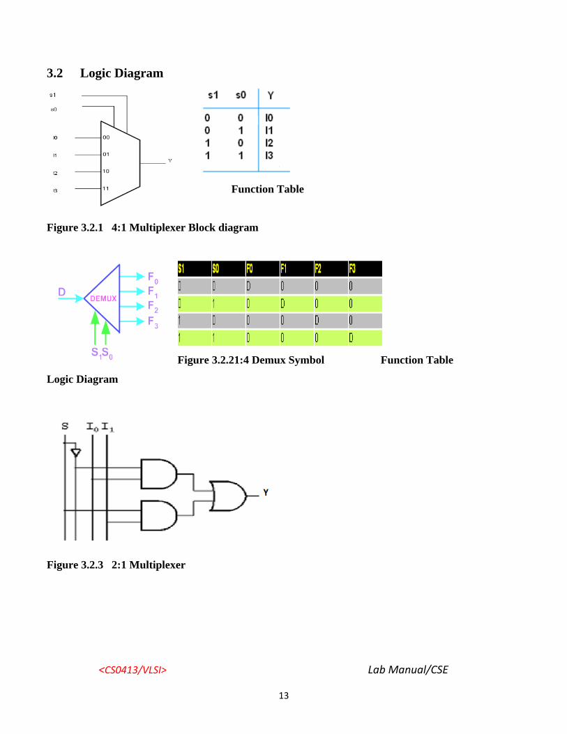
3.2 Logic Diagram
Function Table
Figure 3.2.1 4:1 Multiplexer Block diagram
Figure 3.2.21:4 Demux Symbol Function Table
Logic Diagram
Figure 3.2.3 2:1 Multiplexer

<CS0413/VLSI> Lab Manual/CSE
14
Figure 3.2.4 4:1 Multiplexer
VERILOG Program
Multiplexers 2:1 MUX
Structural Model Dataflow Model BehaviouralModel
module mux21str(i0,i1,s,y);
input i0,i1,s;
output y;
wire net1,net2,net3;
not g1(net1,s);
and g2(net2,i1,s);
and g3(net3,i0,net1);
or g4(y,net3,net2);
endmodule
module mux21df(i0,i1,s,y);
input i0,i1,s;
output y;
assign y =(i0&(~s))|(i1&s);
endmodule
module mux21beh(i0,i1,s,y);
input i0,i1,s;
output y;
reg y;
always@(i0,i1)
begin
if(s==0) y=i1;
if(s==1)y=i0;
end
endmodule
<CS0413/VLSI> Lab Manual/CSE
15
4:1 MUX
Structural Model Dataflow Model BehaviouralModel module mux41str(i0,i1,i2,i3,s0,s1,y); input i0,i1,i2,i3,s0,s1; wire a,b,c,d; output y; and g1(a,i0,s0,s1); and g2(b,i1,(~s0),s1); and g3(c,i2,s0,(~s1)); and g4(d,i3,(~s0),(~s1)); or(y,a,b,c,d); endmodule
module mux41df(i0,i1,i2,i3,s0,s1,y); input i0,i1,i2,i3,s0,s1; output y; assign y=((i0&(~(s0))&(~(s1)))| (i1&(~(s0))&s1)| |(i2&s0&(~(s1)))| (i3&s0&s1); endmodule
module mux41beh(in,s,y ); output y ; input [3:0] in ; input [1:0] s ; reg y; always @ (in,s) begin if (s[0]==0&s[1]==0) y = in[3]; else if (s[0]==0&s[1]==1) y = in[2]; else if (s[0]l==1&s[1]==0) y = in[1]; else y = in[0]; end endmodule
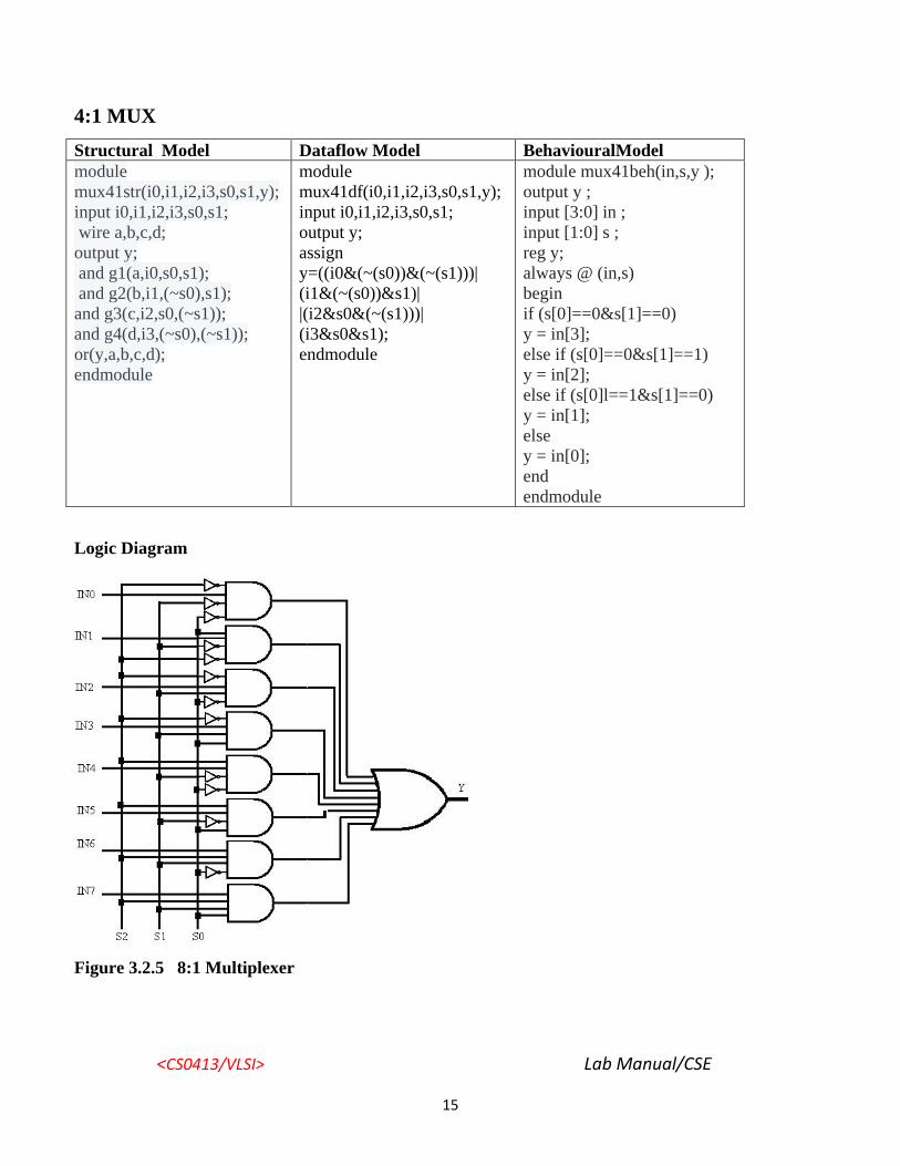
Logic Diagram
Figure 3.2.5 8:1 Multiplexer
<CS0413/VLSI> Lab Manual/CSE
16
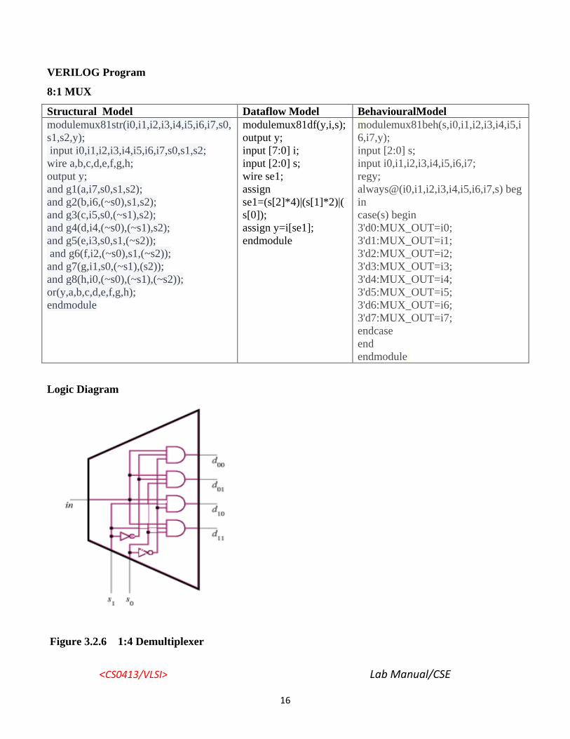
VERILOG Program
8:1 MUX
Structural Model Dataflow Model BehaviouralModel modulemux81str(i0,i1,i2,i3,i4,i5,i6,i7,s0,s1,s2,y); input i0,i1,i2,i3,i4,i5,i6,i7,s0,s1,s2; wire a,b,c,d,e,f,g,h; output y; and g1(a,i7,s0,s1,s2); and g2(b,i6,(~s0),s1,s2); and g3(c,i5,s0,(~s1),s2); and g4(d,i4,(~s0),(~s1),s2); and g5(e,i3,s0,s1,(~s2)); and g6(f,i2,(~s0),s1,(~s2)); and g7(g,i1,s0,(~s1),(s2)); and g8(h,i0,(~s0),(~s1),(~s2)); or(y,a,b,c,d,e,f,g,h); endmodule
modulemux81df(y,i,s); output y; input [7:0] i; input [2:0] s; wire se1; assign se1=(s[2]*4)|(s[1]*2)|(s[0]); assign y=i[se1]; endmodule
modulemux81beh(s,i0,i1,i2,i3,i4,i5,i6,i7,y); input [2:0] s; input i0,i1,i2,i3,i4,i5,i6,i7; regy; always@(i0,i1,i2,i3,i4,i5,i6,i7,s) begin case(s) begin 3'd0:MUX_OUT=i0; 3'd1:MUX_OUT=i1; 3'd2:MUX_OUT=i2; 3'd3:MUX_OUT=i3; 3'd4:MUX_OUT=i4; 3'd5:MUX_OUT=i5; 3'd6:MUX_OUT=i6; 3'd7:MUX_OUT=i7; endcase end endmodule
Logic Diagram
Figure 3.2.6 1:4 Demultiplexer
<CS0413/VLSI> Lab Manual/CSE
17
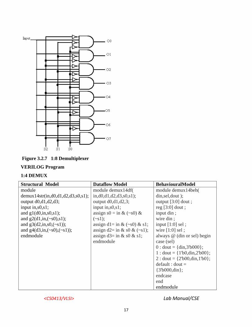
Figure 3.2.7 1:8 Demultiplexer
VERILOG Program
1:4 DEMUX
Structural Model Dataflow Model BehaviouralModel module demux14str(in,d0,d1,d2,d3,s0,s1); output d0,d1,d2,d3; input in,s0,s1; and g1(d0,in,s0,s1); and g2(d1,in,(~s0),s1); and g3(d2,in,s0,(~s1)); and g4(d3,in,(~s0),(~s1)); endmodule
module demux14df( in,d0,d1,d2,d3,s0,s1); output d0,d1,d2,3; input in,s0,s1; assign s0 = in & (~s0) & (~s1); assign d1= in & (~s0) & s1; assign d2= in & s0 & (~s1); assign d3= in & s0 & s1; endmodule
module demux14beh( din,sel,dout ); output [3:0] dout ; reg [3:0] dout ; input din ; wire din ; input [1:0] sel ; wire [1:0] sel ; always @ (din or sel) begin case (sel) 0 : dout = {din,3'b000}; 1 : dout = {1'b0,din,2'b00}; 2 : dout = {2'b00,din,1'b0}; default : dout = {3'b000,din}; endcase end endmodule
<CS0413/VLSI> Lab Manual/CSE
18
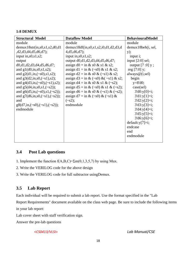
1:8 DEMUX
Structural Model Dataflow Model BehaviouralModel module demux18str(in,s0,s1,s2,d0,d1,d2,d3,d4,d5,d6,d7); input in,s0,s1,s2; output d0,d1,d2,d3,d4,d5,d6,d7; and g1(d0,in,s0,s1,s2); and g2(d1,in,(~s0),s1,s2); and g3(d2,in,s0,(~s1),s2); and g4(d3,in,(~s0),(~s1),s2); and g5(d4,in,s0,s1,(~s2)); and g6(d5,in,(~s0),s1,(~s2)); and g7(d6,in,s0,(~s1),(~s2)); and g8(d7,in,(~s0),(~s1),(~s2)); endmodule
module demux18df(in,s0,s1,s2,i0,d1,d2,d3,d4,d5,d6,d7); input in,s0,s1,s2; output d0,d1,d2,d3,d4,d5,d6,d7; assign d0 = in & s0 & s1 & s2; assign d1 = in & (~s0) & s1 & s2; assign d2 = in & s0 & (~s1) & s2; assign d3 = in & (~s0) &( ~s1) & s2; assign d4 = in & s0 & s1 & (~s2); assign d5 = in & (~s0) & s1 & (~s2); assign d6 = in & s0 & (~s1) & (~s2); assign d7 = in & (~s0) & (~s1) & (~s2); endmodule
module demux18beh(i, sel, y); input i; input [2:0] sel; output [7 :0] y ; reg [7:0] y; always@(i,sel) begin y=8'd0; case(sel) 3'd0:y[0]=i; 3'd1:y[1]=i; 3'd2:y[2]=i; 3'd3:y[3]=i; 3'd4:y[4]=i; 3'd5:y[5]=i; 3'd6:y[6]=i; default:y[7]=i; endcase end endmodule
3.4 Post Lab questions
1. Implement the function f(A,B,C)=Σm(0,1,3,5,7) by using Mux.
2. Write the VERILOG code for the above design
3. Write the VERILOG code for full subtractor usingDemux.
3.5 Lab Report Each individual will be required to submit a lab report. Use the format specified in the "Lab
Report Requirements" document available on the class web page. Be sure to include the following items
in your lab report:
Lab cover sheet with staff verification sign.
Answer the pre-lab questions
<CS0413/VLSI> Lab Manual/CSE
19
Complete VERILOG code design for all logic gates and output signal waveforms
Answer the post-lab questions
3.6 Grading Pre-lab Work 20 points
Lab Performance 30 points
Post-lab Work 20 points
Lab report 30 points
For the lab performance - at a minimum, demonstrate the operation of all the logic gates to your staff in-
charge
The lab report will be graded as follows (for the 30 points):
VERILOG code for each experiments 15 points
Output signal waveform for all experiments and its truth table 15 points
<CS0413/VLSI> Lab Manual/CSE
20
EXP:4 Design of Encoders and Decoders
4.1 Introduction The purpose of this experiment is to introduce you to the basics of Encoders and Decoders. In this lab,
you have to implement Priority Encoder and the Boolean function using Decoders.
Software tools Requirement
Equipments:
Computer with Modelsim Software
Specifications:
HP Computer P4 Processor – 2.8 GHz, 2GB RAM, 160 GB Hard Disk
Softwares: Modelsim - 5.7c, Xilinx - 6.1i.
Algorithm
STEP 1: Open ModelSim XE II / Starter 5.7C
STEP 2: File -> Change directory -> D:\<register number>
STEP 3: File -> New Library -> ok
STEP 4: File -> New Source -> Verilog
STEP 5: Type the program
STEP 6: File -> Save -> <filename.v>
STEP 7: Compile the program
STEP 8: Simulate -> expand work -> select file -> ok
STEP 9: View -> Signals
STEP 10: Select values -> Edit -> Force -> input values
STEP 11: Add -> Wave -> Selected signals -> Run
STEP 12: Change input values and run again
<CS0413/VLSI> Lab Manual/CSE
21
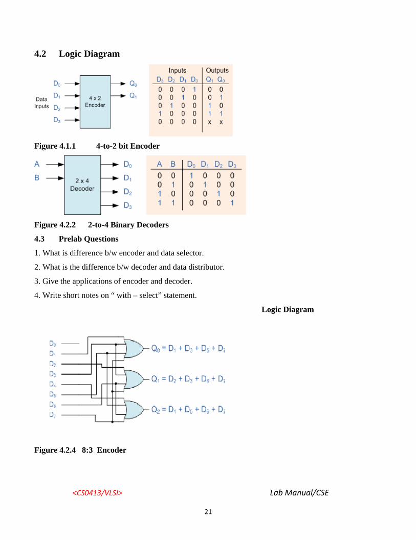
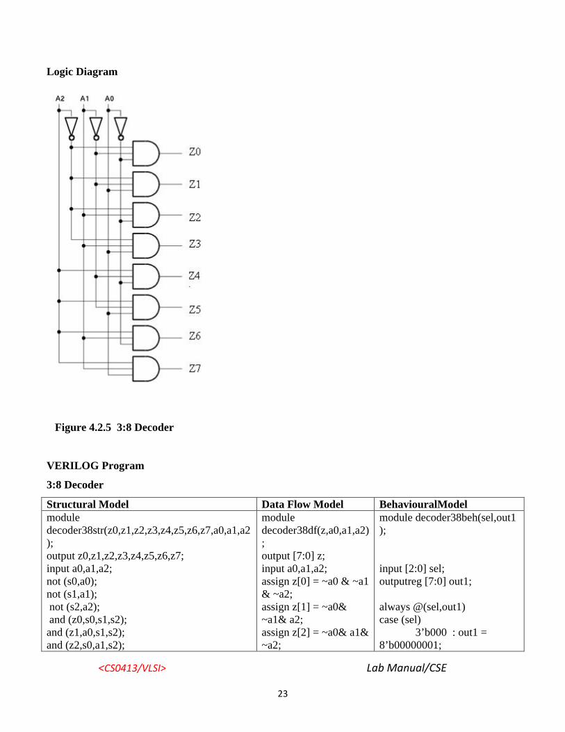
4.2 Logic Diagram
Figure 4.1.1 4-to-2 bit Encoder
Figure 4.2.2 2-to-4 Binary Decoders
4.3 Prelab Questions
1. What is difference b/w encoder and data selector.
2. What is the difference b/w decoder and data distributor.
3. Give the applications of encoder and decoder.
4. Write short notes on “ with – select” statement.
Logic Diagram
Figure 4.2.4 8:3 Encoder
<CS0413/VLSI> Lab Manual/CSE
22
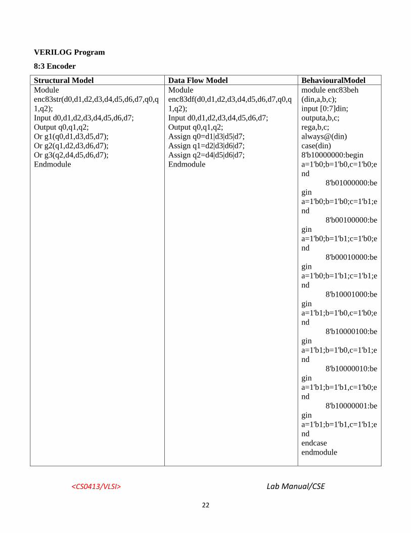
VERILOG Program
8:3 Encoder
Structural Model Data Flow Model BehaviouralModel Module enc83str(d0,d1,d2,d3,d4,d5,d6,d7,q0,q1,q2); Input d0,d1,d2,d3,d4,d5,d6,d7; Output q0,q1,q2; Or g1(q0,d1,d3,d5,d7); Or g2(q1,d2,d3,d6,d7); Or g3(q2,d4,d5,d6,d7); Endmodule
Module enc83df(d0,d1,d2,d3,d4,d5,d6,d7,q0,q1,q2); Input d0,d1,d2,d3,d4,d5,d6,d7; Output q0,q1,q2; Assign q0=d1|d3|d5|d7; Assign q1=d2|d3|d6|d7; Assign q2=d4|d5|d6|d7; Endmodule
module enc83beh (din,a,b,c); input [0:7]din; outputa,b,c; rega,b,c; always@(din) case(din) 8'b10000000:begin a=1'b0;b=1'b0,c=1'b0;end 8'b01000000:begin a=1'b0;b=1'b0;c=1'b1;end 8'b00100000:begin a=1'b0;b=1'b1;c=1'b0;end 8'b00010000:begin a=1'b0;b=1'b1;c=1'b1;end 8'b10001000:begin a=1'b1;b=1'b0,c=1'b0;end 8'b10000100:begin a=1'b1;b=1'b0,c=1'b1;end 8'b10000010:begin a=1'b1;b=1'b1,c=1'b0;end 8'b10000001:begin a=1'b1;b=1'b1,c=1'b1;end endcase endmodule
<CS0413/VLSI> Lab Manual/CSE
23
Logic Diagram
Figure 4.2.5 3:8 Decoder
VERILOG Program
3:8 Decoder
Structural Model Data Flow Model BehaviouralModel module decoder38str(z0,z1,z2,z3,z4,z5,z6,z7,a0,a1,a2); output z0,z1,z2,z3,z4,z5,z6,z7; input a0,a1,a2; not (s0,a0); not (s1,a1); not (s2,a2); and (z0,s0,s1,s2); and (z1,a0,s1,s2); and (z2,s0,a1,s2);
module decoder38df(z,a0,a1,a2); output [7:0] z; input a0,a1,a2; assign z[0] = ~a0 & ~a1 & ~a2; assign z[1] = ~a0& ~a1& a2; assign z[2] = ~a0& a1& ~a2;
module decoder38beh(sel,out1); input [2:0] sel; outputreg [7:0] out1; always @(sel,out1) case (sel) 3’b000 : out1 = 8’b00000001;
<CS0413/VLSI> Lab Manual/CSE
24
and z3,a0,a1,s2); and (z4,s0,s1,a2); and (z5,a0,s1,a2); and (z6,s0,a1,a2); and (z7,a0,a1,a2); endmodule
assign z[3] = ~a0& a1& a2; assign z[4] = a0& ~a1& ~a2; assign z[5] = a0& ~a1& a2; assign z[6] = a0& a1& ~a2; assign z[7] = a0& a1& a2; endmodule
3’b001 : out1 = 8’b00000010; 3’b010 : out1 = 8’b00000100; 3’b011 : out1 = 8’b00001000; 3’b100 : out1 = 8’b00010000; 3’b101 : out1 = 8’b00100000; 3’b110 : out1 = 8’b01000000; default : out1 = 8’b10000000; endcase endmodule
4.4 Post Lab questions
1. Implement full adder by using suitable decoder.
2. Write the VERILOG code for the above design
3. Write the VERILOG code for 3 bit Gray to binary code converter.
4. Write short notes on “test bench” with examples.
4.5 Lab Report
Each individual will be required to submit a lab report. Use the format specified in the "Lab
Report Requirements"document available on the class web page. Be sure to include the following items in
your lab report:
Lab cover sheet with staff verification sign.
Answer the pre-lab questions
Complete VERILOG code design for all logic gates and output signal waveforms
Answer the post-lab questions
<CS0413/VLSI> Lab Manual/CSE
25
4.6 Grading
Pre-lab Work 20 points
Lab Performance 30 points
Post-lab Work 20 points
Lab report 30 points
For the lab performance - at a minimum, demonstrate the operation of all the logic gates to your staff in-
charge
The lab report will be graded as follows (for the 30 points):
VERILOG code for each experiments 15 points
Output signal waveform for all experiments and its truth table 15 point

<CS0413/VLSI> Lab Manual/CSE
26
EXP 5: Flip Flops
5.1 Introduction The purpose of this experiment is to introduce you to the basics of flip-flops. In this lab, you will test the
behavior of several flip-flops and you will connect several logic gates together to create simple sequential
circuits.
5.2 Software tools Requirement
Equipments:
Computer with Modelsim Software
Specifications:
HP Computer P4 Processor – 2.8 GHz, 2GB RAM, 160 GB Hard Disk
Softwares: Modelsim - 5.7c, Xilinx - 6.1i.
Algorithm
STEP 1: Open ModelSim XE II / Starter 5.7C
STEP 2: File -> Change directory -> D:\<register number>
STEP 3: File -> New Library -> ok
STEP 4: File -> New Source -> Verilog
STEP 5: Type the program
STEP 6: File -> Save -> <filename.v>
STEP 7: Compile the program
STEP 8: Simulate -> expand work -> select file -> ok
STEP 9: View -> Signals
STEP 10: Select values -> Edit -> Force -> input values
STEP 11: Add -> Wave -> Selected signals -> Run
STEP 12: Change input values and run again
5.2 Flip-Flops Logic diagram and their properties Flip-flops are synchronous bitable devices. The term synchronous means the output changes state only
when the clock input is triggered. That is, changes in the output occur in synchronization with the clock.
<CS0413/VLSI> Lab Manual/CSE
27
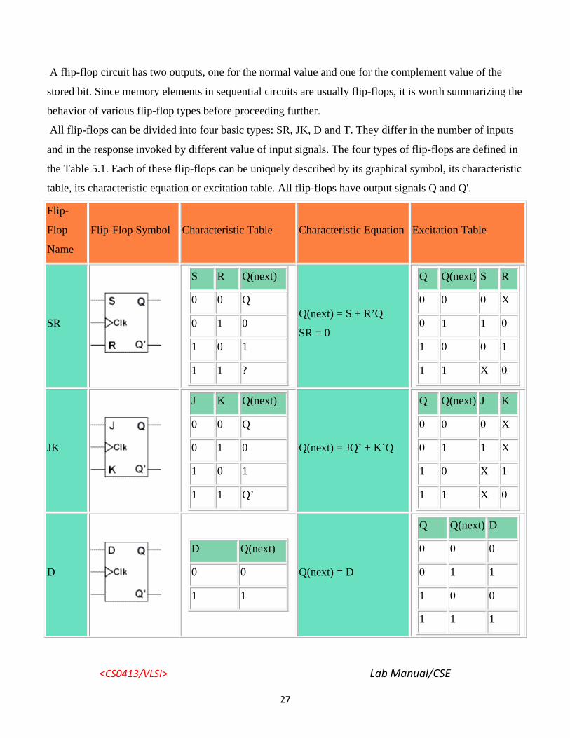
A flip-flop circuit has two outputs, one for the normal value and one for the complement value of the
stored bit. Since memory elements in sequential circuits are usually flip-flops, it is worth summarizing the
behavior of various flip-flop types before proceeding further.
All flip-flops can be divided into four basic types: SR, JK, D and T. They differ in the number of inputs
and in the response invoked by different value of input signals. The four types of flip-flops are defined in
the Table 5.1. Each of these flip-flops can be uniquely described by its graphical symbol, its characteristic
table, its characteristic equation or excitation table. All flip-flops have output signals Q and Q'.
Flip-
Flop
Name
Flip-Flop Symbol Characteristic Table Characteristic Equation Excitation Table
SR
S R Q(next)
0 0 Q
0 1 0
1 0 1
1 1 ?
Q(next) = S + R’Q
SR = 0
Q Q(next) S R
0 0 0 X
0 1 1 0
1 0 0 1
1 1 X 0
JK
J K Q(next)
0 0 Q
0 1 0
1 0 1
1 1 Q’
Q(next) = JQ’ + K’Q
Q Q(next) J K
0 0 0 X
0 1 1 X
1 0 X 1
1 1 X 0
D
D Q(next)
0 0
1 1
Q(next) = D
Q Q(next) D
0 0 0
0 1 1
1 0 0
1 1 1
<CS0413/VLSI> Lab Manual/CSE
28
T
T Q(next)
0 Q
1 Q’
Q(next) = TQ’ + T’Q
Q Q(next) T
0 0 0
0 1 1
1 0 1
1 1 0
Table 5.2 Flip-flops and their properties
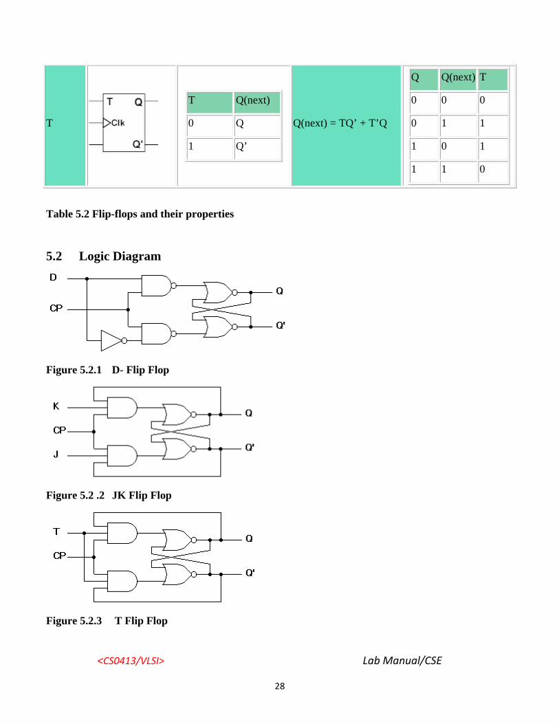
5.2 Logic Diagram
Figure 5.2.1 D- Flip Flop
Figure 5.2 .2 JK Flip Flop
Figure 5.2.3 T Flip Flop
<CS0413/VLSI> Lab Manual/CSE
29
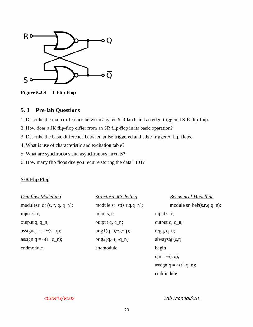
Figure 5.2.4 T Flip Flop
5. 3 Pre-lab Questions 1. Describe the main difference between a gated S-R latch and an edge-triggered S-R flip-flop.
2. How does a JK flip-flop differ from an SR flip-flop in its basic operation?
3. Describe the basic difference between pulse-triggered and edge-triggered flip-flops.
4. What is use of characteristic and excitation table?
5. What are synchronous and asynchronous circuits?
6. How many flip flops due you require storing the data 1101?
S-R Flip Flop
Dataflow Modelling Structural Modelling Behavioral Modelling
modulesr_df (s, r, q, q_n); module sr_st(s,r,q,q_n); module sr_beh(s,r,q,q_n);
input s, r; input s, r; input s, r;
output q, q_n; output q, q_n; output q, q_n;
assignq_n = ~(s | q); or g1(q_n,~s,~q); regq, q_n;
assign q = ~(r | q_n); or g2(q,~r,~q_n); always@(s,r)
endmodule endmodule begin
q,n = ~(s|q);
assign q = ~(r | q_n);
endmodule
<CS0413/VLSI> Lab Manual/CSE
30
T Flip Flop
Behavioral Modelling Structural Modelling Dataflow Modelling
module t_beh(q,q1,t,c); module t_st(q,q1,t,c); module t_df(q,q,1,t,c);
output q,q1; output q,q1; output q,q1;
inputt,c; input t,c; input t,c;
reg q,q1; wire w1,w2; and g1(w1,t,c,q);
initial assign w1=t&c&q; and g2(w2,t,c,q1);
begin assign w2=t&c&q1; nor g3(q,w1,q1);
q=1'b1; assign q=~(w1|q1); nor g4(q1,w2,q);
q1=1'b0; assign q1=~(w2|q); endmodule
end endmodule
always @ (c)
begin
if(c)
begin
if (t==1'b0) begin q=q; q1=q1; end
else begin q=~q; q1=~q1; end
end
end
endmodule
<CS0413/VLSI> Lab Manual/CSE
31
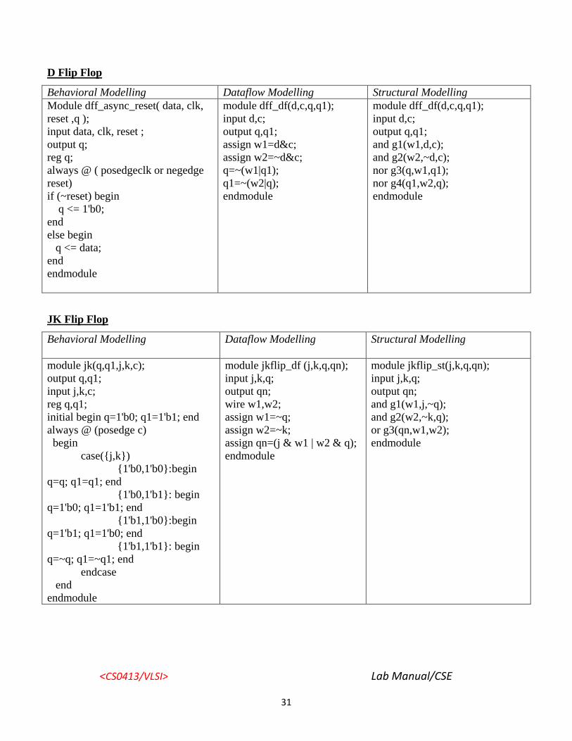
D Flip Flop
Behavioral Modelling Dataflow Modelling Structural Modelling Module dff_async_reset( data, clk, reset ,q ); input data, clk, reset ; output q; reg q; always @ ( posedgeclk or negedge reset) if (~reset) begin q <= 1'b0; end else begin q <= data; end endmodule
module dff_df(d,c,q,q1); input d,c; output q,q1; assign w1=d&c; assign w2=~d&c; q=~(w1|q1); q1=~(w2|q); endmodule
module dff_df(d,c,q,q1); input d,c; output q,q1; and g1(w1,d,c); and g2(w2,~d,c); nor g3(q,w1,q1); nor g4(q1,w2,q); endmodule
JK Flip Flop
Behavioral Modelling Dataflow Modelling
Structural Modelling
module jk(q,q1,j,k,c); output q,q1; input j,k,c; reg q,q1; initial begin q=1'b0; q1=1'b1; end always @ (posedge c) begin case({j,k}) {1'b0,1'b0}:begin q=q; q1=q1; end {1'b0,1'b1}: begin q=1'b0; q1=1'b1; end {1'b1,1'b0}:begin q=1'b1; q1=1'b0; end {1'b1,1'b1}: begin q=~q; q1=~q1; end endcase end endmodule
module jkflip_df (j,k,q,qn); input j,k,q; output qn; wire w1,w2; assign w1=~q; assign w2=~k; assign qn=(j & w1 | w2 & q); endmodule
module jkflip_st(j,k,q,qn); input j,k,q; output qn; and g1(w1,j,~q); and g2(w2,~k,q); or g3(qn,w1,w2); endmodule
<CS0413/VLSI> Lab Manual/CSE
32
5.4 Post lab
1. Discuss the application of flip-flops in data storage.
2. Draw the logic diagram of Master Slave JK flip-flop.
3. A flip-flop is presently in the RESET state and must go to the SET state on the next clock pulse. What
must J and K be?
4. What do you know about clk and clk event in VERILOG?
5. Convert the following.
a. JK to T f/f
b. SR to D
6. Write the VERILOG code for question no 5.
5.5 Lab Report Each individual will be required to submit a lab report. Use the format specified in the "Lab
Report Requirements" document available on the class web page. Be sure to include the following items
in your lab report:
Lab cover sheet with staff verification for circuit diagram
Answer the pre-lab questions
Complete paper design for all three designs including K-maps and minimized equations and the truth
table for each of the output signals.
Answer the post-lab questions
5.6 Grading Pre-lab Work 20 points
Lab Performance 30 points
Post-lab Work 20 points
Lab report 30 points
For the lab performance - at a minimum, demonstrate the operation of all the circuits to your staff in-
charge
The lab report will be graded as follows (for the 30 points):
VERILOG code for each experiments 15 points

<CS0413/VLSI> Lab Manual/CSE
33
Output signal waveform for all experiments and its truth table 15 points
<CS0413/VLSI> Lab Manual/CSE
34
EXP 6: COUNTERS
6.1 Introduction The purpose of this experiment is to introduce the design of Synchronous Counters. The student
should also be able to design n-bit up/down Counter.
6.2 Software tools Requirement Equipments:
Computer with Modelsim Software
Specifications:
HP Computer P4 Processor – 2.8 GHz, 2GB RAM, 160 GB Hard Disk
Softwares: Modelsim - 5.7c, Xilinx - 6.1i.
Algorithm
STEP 1: Open ModelSim XE II / Starter 5.7C
STEP 2: File -> Change directory -> D:\<register number>
STEP 3: File -> New Library -> ok
STEP 4: File -> New Source -> Verilog
STEP 5: Type the program
STEP 6: File -> Save -> <filename.v>
STEP 7: Compile the program
STEP 8: Simulate -> expand work -> select file -> ok
STEP 9: View -> Signals
STEP 10: Select values -> Edit -> Force -> input values
STEP 11: Add -> Wave -> Selected signals -> Run
STEP 12: Change input values and run again
<CS0413/VLSI> Lab Manual/CSE
35
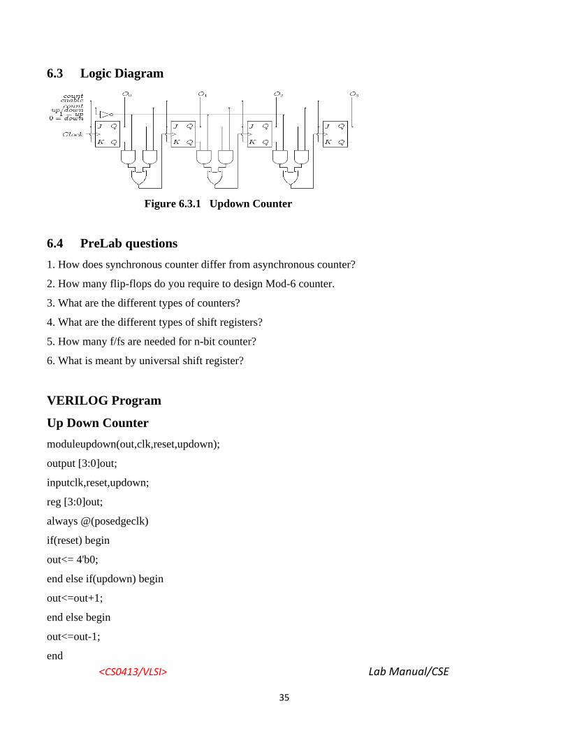
6.3 Logic Diagram
Figure 6.3.1 Updown Counter
6.4 PreLab questions 1. How does synchronous counter differ from asynchronous counter?
2. How many flip-flops do you require to design Mod-6 counter.
3. What are the different types of counters?
4. What are the different types of shift registers?
5. How many f/fs are needed for n-bit counter?
6. What is meant by universal shift register?
VERILOG Program
Up Down Counter moduleupdown(out,clk,reset,updown);
output [3:0]out;
inputclk,reset,updown;
reg [3:0]out;
always @(posedgeclk)
if(reset) begin
out<= 4'b0;
end else if(updown) begin
out<=out+1;
end else begin
out<=out-1;
end

<CS0413/VLSI> Lab Manual/CSE
36
endmodule
6.5 Post Lab questions 1. Write the use of enable and reset signal.
2. What is the function of generic statement?
3. Design mod-6 counter using d flf and write the VERILOG code.
6.6 Lab Report Each individual will be required to submit a lab report. Use the format specified in the Lab
Report Requirements document available on the class web page. Be sure to include the following items in
your lab report:
Lab cover sheet with staff verification for circuit diagram
Answer the pre-lab questions
Complete paper design for all three designs including K-maps and minimized equations and the truth
table for each of the output signals.
Answer the post-lab questions
6.7 Grading Pre-lab Work 20 points
Lab Performance 30 points
Post-lab Work 20 points
Lab report 30 points
For the lab performance - at a minimum, demonstrate the operation of all the circuits to your staff in-
charge
The lab report will be graded as follows (for the 30 points):
VERILOG code for each experiments 15 points
Output signal waveform for all experiments and its truth table 15 points
<CS0413/VLSI> Lab Manual/CSE
37
EXP 7: BITWISE OPERATORS USING 8051 7.1 Introduction The purpose of this experiment is to implement bitwise operators using 8051. The student should also be
able to implement Logical Operations in 8051.
7.2 Software tools Requirement Equipments:
Computer with Keil µversion II Software
Specifications:
HP Computer P4 Processor – 2.8 GHz, 2GB RAM, 160 GB Hard Disk
Softwares: Keil µversion II
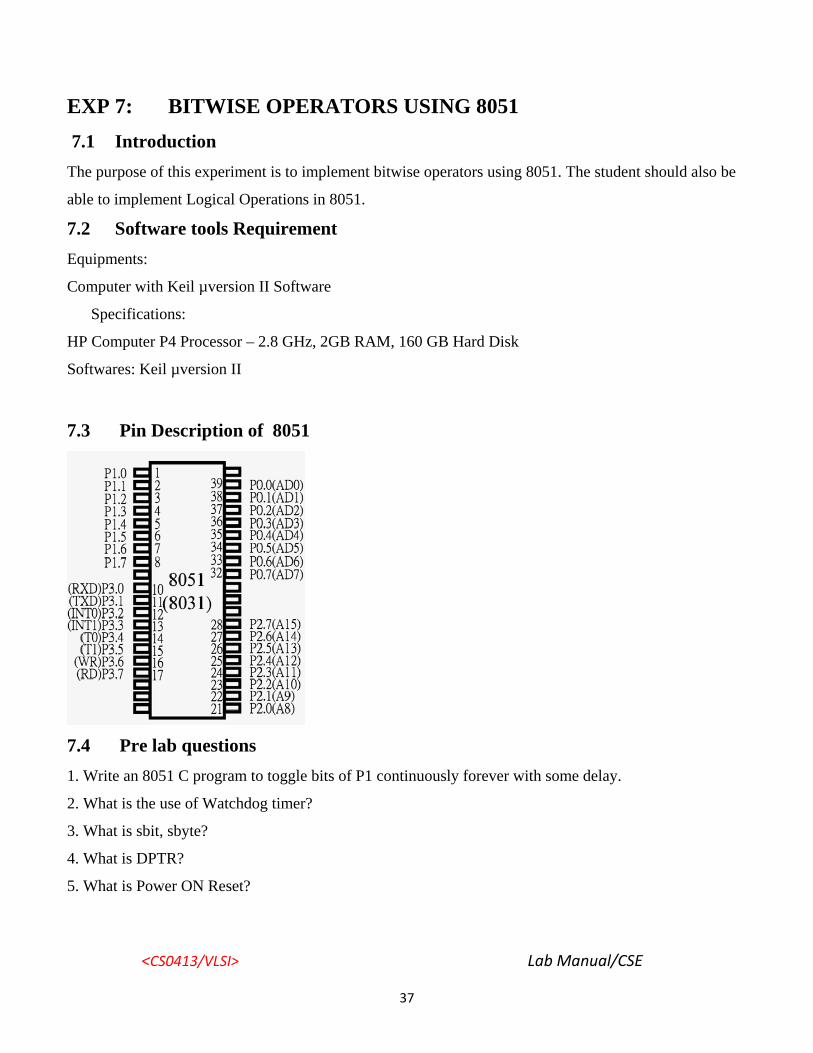
7.3 Pin Description of 8051
7.4 Pre lab questions 1. Write an 8051 C program to toggle bits of P1 continuously forever with some delay.
2. What is the use of Watchdog timer?
3. What is sbit, sbyte?
4. What is DPTR?
5. What is Power ON Reset?
<CS0413/VLSI> Lab Manual/CSE
38
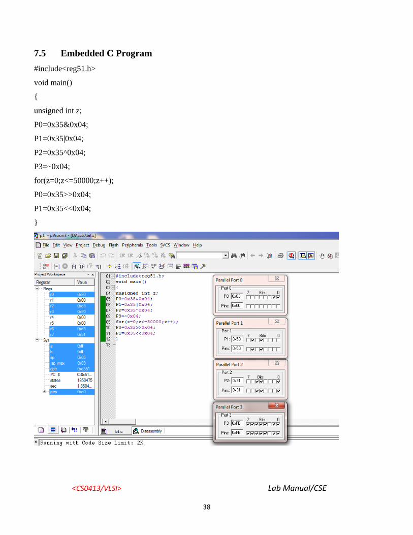
7.5 Embedded C Program
#include<reg51.h>
void main()
{
unsigned int z;
P0=0x35&0x04;
P1=0x35|0x04;
P2=0x35^0x04;
P3=~0x04;
for(z=0;z<=50000;z++);
P0=0x35>>0x04;
P1=0x35<<0x04;
}
<CS0413/VLSI> Lab Manual/CSE
39
7.6 Post lab: 1. Design a Calculator using 8051.
2. Write the Embedded C Program for the above.
3. Write the Embedded C Program for Bit Operations.
7.7 Lab Report Each individual will be required to submit a lab report. Use the format specified in the "Lab
Report Requirements" document available on the class web page. Be sure to include the following items
in your lab report:
Lab cover sheet with staff verification for circuit diagram
Answer the pre-lab questions
Complete paper design for all three designs including K-maps and minimized equations and the truth
table for each of the output signals.
Answer the post-lab questions
7.8 Grading Pre-lab Work 20 points
Lab Performance 30 points
Post-lab Work 20 points
Lab report 30 points
For the lab performance - at a minimum, demonstrate the operation of all the circuits to your staff in-
charge
The lab report will be graded as follows (for the 30 points):
Embedded C code for each experiments 15 points
Output signal for all experiments and its model calculation 15 points

<CS0413/VLSI> Lab Manual/CSE
40
EXP 8: TOGGLE A PORT BIT IN 8051
8.1 Introduction The purpose of this experiment is to Toggle a Port bit in 8051. The student should also be able to control
Port Pin in 8051.
8.2 Software tools Requirement Equipments:
Computer with Keil µversion II Software
Specifications:
HP Computer P4 Processor – 2.8 GHz, 2GB RAM, 160 GB Hard Disk
Softwares: Keil µversion II
8.3 Pre lab questions 1. Write an 8051 C program to toggle bits of P1 continuously forever with some delay.
2. What is the use of Watchdog timer?
3. What is sbit, sbyte?
4. What is DPTR?
5. What is Power ON Reset?
8.4 Embedded C Program #include<reg51.h>
sbit Mybit=P1^0;
void main()
{
while(1)
{
unsigned int z;
Mybit=0;
for(z=0;z<=5000;z++);
Mybit=1;
<CS0413/VLSI> Lab Manual/CSE
41
for(z=0;z<=5000;z++);
}
}
8.5 Post lab: 1. A door sensor is connected to the P1.1 pin, and a buzzer is connected
to P1.7. Write an 8051 C program to monitor the door sensor, and
when it opens, sound the buzzer. You can sound the buzzer by
sending a square wave of a few hundred Hz.
2. Write an 8051 C program to get the status of bit P1.0, save it, and
send it to P2.7 continuously.
8.6 Lab Report Each individual will be required to submit a lab report. Use the format specified in the "Lab
Report Requirements" document available on the class web page. Be sure to include the following items
in your lab report:
Lab cover sheet with staff verification for circuit diagram

<CS0413/VLSI> Lab Manual/CSE
42
Answer the pre-lab questions
Complete paper design for all three designs including K-maps and minimized equations and the truth
table for each of the output signals.
Answer the post-lab questions
8.7 Grading Pre-lab Work 20 points
Lab Performance 30 points
Post-lab Work 20 points
Lab report 30 points
For the lab performance - at a minimum, demonstrate the operation of all the circuits to your staff in-
charge
The lab report will be graded as follows (for the 30 points):
Embedded C code for each experiments 15 points
Output signal for all experiments and its model calculation 15 points

<CS0413/VLSI> Lab Manual/CSE
43
EXP 9: DELAY OPERATORS IN 8051
9.1 Introduction The purpose of this experiment is to introduce delay operators 8051. The student should also be able to
write ISR for various Interrupts in 8051.
9.2 Software tools Requirement Equipments:
Computer with Keil µversion II Software
Specifications:
HP Computer P4 Processor – 2.8 GHz, 2GB RAM, 160 GB Hard Disk
Softwares: Keil µversion II
9.3 Pre lab questions 1. Write an 8051 C program to gets a single bit of data from P1.7 and sends it to P1.0.
2. What is ISR?
3. Name the two ways to access Interrupts?
4. What is Power ON Reset?
9.4 Embedded C Program #include<reg51.h>
void todelay(void)
{
TMOD=0x01;
TL0=0x08;
TR0=1;
TH0=0xEF;
}
void main()
{
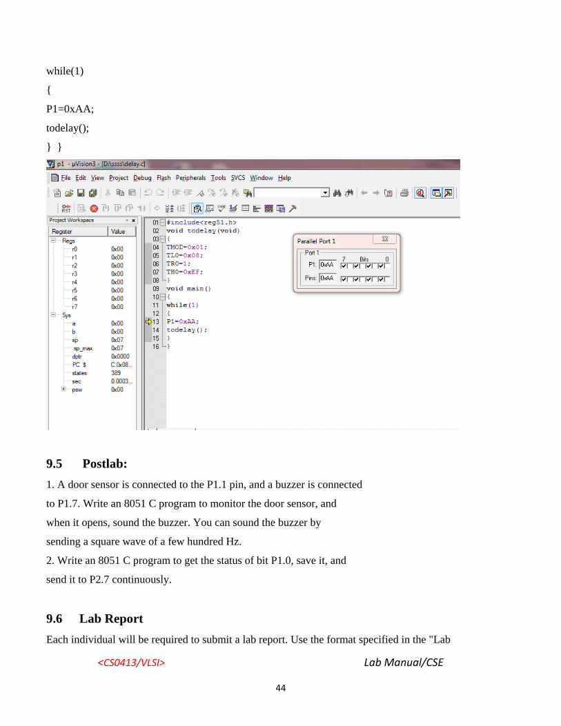
<CS0413/VLSI> Lab Manual/CSE
44
while(1)
{
P1=0xAA;
todelay();
} }
9.5 Postlab: 1. A door sensor is connected to the P1.1 pin, and a buzzer is connected
to P1.7. Write an 8051 C program to monitor the door sensor, and
when it opens, sound the buzzer. You can sound the buzzer by
sending a square wave of a few hundred Hz.
2. Write an 8051 C program to get the status of bit P1.0, save it, and
send it to P2.7 continuously.
9.6 Lab Report Each individual will be required to submit a lab report. Use the format specified in the "Lab
<CS0413/VLSI> Lab Manual/CSE
45
Report Requirements" document available on the class web page. Be sure to include the following items
in your lab report:
Lab cover sheet with staff verification for circuit diagram
Answer the pre-lab questions
Complete paper design for all three designs including K-maps and minimized equations and the truth
table for each of the output signals.
Answer the post-lab questions
9.7 Grading Pre-lab Work 20 points
Lab Performance 30 points
Post-lab Work 20 points
Lab report 30 points
For the lab performance - at a minimum, demonstrate the operation of all the circuits to your staff in-
charge
The lab report will be graded as follows (for the 30 points):
Embedded C code for each experiments 15 points
Output signal for all experiments and its model calculation 15 points


![DEPARTMENT OF COMPUTER SCIENCE AND ENGINEERING LAB … · DEPARTMENT OF COMPUTER SCIENCE AND ENGINEERING LAB MANUAL ... int a[10]; void main() {inti; printf("enter the array"); for](https://static.fdocuments.us/doc/165x107/5ac4ba047f8b9ae06c8d6671/department-of-computer-science-and-engineering-lab-of-computer-science-and-engineering.jpg)