


DEMO MANUAL DC1366B LTC4266 IEEE 802.3at PoE Quad PSE ... · PSE system is the power management...
18
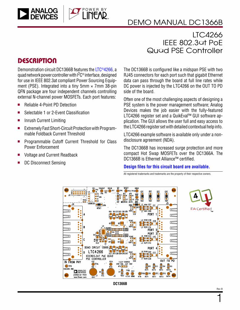
1 Rev B DEMO MANUAL DC1366B DESCRIPTION LTC4266 IEEE 802.3at PoE Quad PSE Controller Demonstration circuit DC1366B features the LTC ® 4266, a quad network power controller with I 2 C ® interface, designed for use in IEEE 802.3at compliant Power Sourcing Equip- ment (PSE). Integrated into a tiny 5mm × 7mm 38-pin QFN package are four independent channels controlling external N-channel power MOSFETs. Each port features: n Reliable 4-Point PD Detection n Selectable 1 or 2-Event Classification n Inrush Current Limiting n Extremely Fast Short-Circuit Protection with Program- mable Foldback Current Threshold n Programmable Cutoff Current Threshold for Class Power Enforcement n Voltage and Current Readback n DC Disconnect Sensing The DC1366B is configured like a midspan PSE with two RJ45 connectors for each port such that gigabit Ethernet data can pass through the board at full line rates while DC power is injected by the LTC4266 on the OUT TO PD side of the board. Often one of the most challenging aspects of designing a PSE system is the power management software; Analog Devices makes the job easier with the fully-featured LTC4266 register set and a QuikEval™ GUI software ap- plication. The GUI allows the user full and easy access to the LTC4266 register set with detailed contextual help info. LTC4266 example software is available only under a non- disclosure agreement (NDA). The DC1366B has increased surge protection and more compact Hot Swap MOSFETs over the DC1366A. The DC1366B is Ethernet Alliance™ certified. Design files for this circuit board are available. DC1366B All registered trademarks and trademarks are the property of their respective owners.
Transcript of DEMO MANUAL DC1366B LTC4266 IEEE 802.3at PoE Quad PSE ... · PSE system is the power management...
1Rev B
DEMO MANUAL DC1366B
DESCRIPTION
LTC4266 IEEE 802.3at PoE
Quad PSE Controller
Demonstration circuit DC1366B features the LTC®4266, a quad network power controller with I2C® interface, designed for use in IEEE 802.3at compliant Power Sourcing Equip-ment (PSE). Integrated into a tiny 5mm × 7mm 38-pin QFN package are four independent channels controlling external N-channel power MOSFETs. Each port features:n Reliable 4-Point PD Detectionn Selectable 1 or 2-Event Classificationn Inrush Current Limitingn Extremely Fast Short-Circuit Protection with Program-
mable Foldback Current Thresholdn Programmable Cutoff Current Threshold for Class
Power Enforcementn Voltage and Current Readbackn DC Disconnect Sensing
The DC1366B is configured like a midspan PSE with two RJ45 connectors for each port such that gigabit Ethernet data can pass through the board at full line rates while DC power is injected by the LTC4266 on the OUT TO PD side of the board.
Often one of the most challenging aspects of designing a PSE system is the power management software; Analog Devices makes the job easier with the fully-featured LTC4266 register set and a QuikEval™ GUI software ap-plication. The GUI allows the user full and easy access to the LTC4266 register set with detailed contextual help info.
LTC4266 example software is available only under a non-disclosure agreement (NDA).
The DC1366B has increased surge protection and more compact Hot Swap MOSFETs over the DC1366A. The DC1366B is Ethernet Alliance™ certified.
Design files for this circuit board are available.
DC1366B
All registered trademarks and trademarks are the property of their respective owners.

2Rev B
DEMO MANUAL DC1366B
QUICK START PROCEDUREFigure 1 shows the basic setup. The LTC4266 requires two power supply rails: VDD (nominally 3.3V) and VEE (nominally –54V). The VDD supply can be provided by a DC590 board or an external bench supply.
When running QuikEval on a Windows computer, the DC590 is used to interface a USB port on the PC to the I2C bus on the DC1366B. The DC590 also provides opto-isolation of the I2C bus, and an isolated 3.3V supply to run the LTC4266; the user need only provide the VEE supply.
Alternatively, the user can omit the DC590 and connect an I2C master device to the DC1366B. If the DC590 is omitted then a bench power supply must provide VDD.
For applications where I2C control is not required, the LTC4266 features an AUTO mode allowing it to operate completely autonomously.
Choose one of the setup procedures shown on the next page, depending on whether or not the QuikEval GUI ap-plication software is required.
Setup Procedure to Run the QuikEval GUI Software
1. Install the GUI software on the PC according to the instructions in the README.txt file included with the GUI software.
2. On the DC590:
a. Set both sides (ISO and SW) of JP5 to ON.
b. Set JP6 to 3.3V.
3. Connect the DC590 to the PC with a standard USB A-B cable.
a. Verify the computer recognized the USB device. (The first time the DC590 is connected the Hardware Wizard may ask for help to locate the driver. Direct it to the location specified in the README.txt that came with the GUI software.)
b. Verify the ISO PWR LED on the DC590 is lit.
4. On the DC1366B board:
a. Set JP5 to the USB VDD position.
b. Set JP3 to the TIE position.
c. Set JP4 (AUTO) to the HI position.
d. If midspan operation is desired set JP2 to HI, for endpoint set to LO.
5. Connect the DC590 to the DC1366B with the 14-con-ductor ribbon cable supplied with the DC1366B. Verify the VDD LED on the DC1366B is lit.
6. Before connecting the main power supply to the DC1366B verify the voltage is between 51V and 57V, and that the main supply is turned off.
7. Connect the main power supply to the DC1366B with two banana patch cords as shown in Figure 1. Verify the polarity is correct before turning on the power; positive goes to RTN and negative to VEE.
8. Turn on the main power supply and verify the VEE LED on the DC1366B is lit.
9. Connect PDs to any of the ports on the OUT to PD side of the DC1366B and verify they turn on by the respective OUTn LED.
10. Launch QuikEval.

3Rev B
DEMO MANUAL DC1366B
QUICK START PROCEDURESetup Procedure without the DC590
1. On the DC1366B:
a. Set JP5 to EXT VDD.
b. Set JP4 (AUTO) to the HI position.
c. If midspan operation is desired set JP2 to HI, for endpoint set to LO.
2. Connect a 3.3V power supply across +3.3V and DGND test points as shown in Figure 1. Turn on the 3.3V supply and verify the VDD LED on the DC1366B is lit.
3. Before connecting the main power supply to the DC1366B verify the voltage is between 51V and 57V, and that the main supply is turned off.
4. Connect the main power supply to the DC1366B with two banana patch cords as shown in Figure 1. Verify the polarity is correct before turning on the power; positive goes to RTN and negative to VEE.
5. Turn on the main power supply and verify the VEE LED on the DC1366B is lit.
6. Connect PDs to any of the ports on the OUT TO PD side of the DC1366B and verify they turn on by the respective OUTn LED.

4Rev B
DEMO MANUAL DC1366B
QUICK START PROCEDURE
IsolatedVEE Supply(51V to 57V)
OptionalVDD Supply(3.3V Nominal)
+– –+
RJ45 RJ45 PD1
CAT5Cables
RJ45 RJ45 PD2
RJ45 RJ45 PD3
RJ45 RJ45 PD4
DC590USB to I2CInterface
WindowsComputer
14-Pin Ribbon Cable
Optional Equipment for Computer Control
USB CABLE
Figure 1. DC1366B Setup
5Rev B
DEMO MANUAL DC1366B
OPERATIONIntroduction
The DC1366B demonstrates the features and capabilities of the LTC4266, a quad controller for IEEE802.3at Power Sourcing Equipment (PSE). The DC1366B provides a quick and simple, fully compliant PSE solution requiring only a VEE supply when used in conjunction with the DC590 USB-to-I2C interface board.
Supply Voltages
The IEEE802.3at standard requires the port output volt-age of a type 2 PSE to be in the range of 50V to 57V. The positive side is RTN and the negative side is VEE. The VEE supply voltage should be in this range for the sake of compliance; however, the LTC4266 is capable of operat-ing with VEE down to 30V, the max undervoltage lockout (UVLO) threshold.
Make sure to choose a VEE supply with enough power to sustain all four ports at maximum load; if the total load is too great for the power supply its voltage may drop below the UVLO threshold, resetting the LTC4266 and shutting off all the ports. The worst case is when all four PDs are class 4: each class 4 PD may draw up to 600mA, totaling 2.4A. Therefore a VEE supply rated for at least 2.6A is recommended.
The VDD supply should nominally be 3.3V but the LTC4266 is capable of operating over the range of 3.0V to 4.3V. (The UVLO threshold for the VDD supply is typically 2.2V.) The LTC4266 chip typically draws only 1.1mA from the VDD supply; however, LEDs and other components on the DC1366B board also draw current from VDD, so the total load is typically 9mA to 26mA at 3.3V depending on which LEDs are lit.
VDD to DGND Configurations
The DC1366B, LTC4266 VDD supply can be configured in one of two ways. The default DC1366B configuration ties the LTC4266 VDD pin to the AGND pin through a 0 Ohm resistor R10. The DGND pin is at –3.3V below the AGND pin. The DC1366B can also be configured for a +3.3V at VDD relative to AGND by removing R10 and installing a 0Ω resistor at R9. This ties the LTC4266 DGND pin and AGND pin.
Modes of Operation
The LTC4266 has four modes of operation:n Shutdown: Ports are shutdown, detection and clas-
sification cycles are disabled.n Manual: The port does not advance automatically from
detection to classification, to power on. It waits for instructions from a host controller via the I2C interface.
n Semiauto: The port automatically advances to clas-sification after detecting a PD, but does not turn on power to the PD until told to do so by from a host controller via the I2C interface.
n AUTO Pin High: The LTC4266 operates autonomously.
AUTO Pin
The AUTO pin determines several aspects of the LTC4266 initial behavior. AUTO is sensed by the LTC4266 at power up and after a reset.
If the AUTO pin is high then:n All ports come up in AUTO pin high mode. Any valid
PD will be turned on without software intervention.n The current-sense resistors are assumed to be 0.25Ω
(which they are on the DC1366B).n High power is enabled. After the LTC4266 classifies a
PD it applies power and automatically sets ICUT and ILIM appropriately for the class. With high-power enabled a class 4 PD will be able to draw up to 600mA without being cut off.
If the AUTO pin is low then:n All ports come up in shutdown mode. A host controller
must take action in order to power up any PDs.n The current-sense resistors are assumed to be 0.50Ω;
a host controller must change this to 0.25Ω for correct operation of the DC1366B.
n High power is disabled and is enabled by a host con-troller.

6Rev B
DEMO MANUAL DC1366B
OPERATIONEndpoint vs. Midspan
The LTC4266 can be configured either for endpoint or midspan operation without software intervention by setting the MID pin high or low respectively. (You must reset the LTC4266 or cycle the power for the MID pin to be sensed.) The only difference in the behavior of the LTC4266 is that the detection back-off timer is enabled when midspan operation is selected.
Each port can be configured individually as either endspan or midspan via I2C commands.
The DC1366B is wired for Alternative-A, MDI-X (power is injected on the data pairs of the CAT5/6e cable; positive on pins 3 and 6 of the RJ45 connector, and negative on pins 1 and 2). The original 802.3af standard required all midspans to use Alternative-B, but 802.3at allows midspans to use Alternative-A.
Disconnect Sensing
The LTC4266 employs DC disconnect sensing only. For the sake of software backward compatibility with the older LTC4259, the LTC4266 includes register bits for enabling AC disconnect sensing, but these bits simply enable the DC disconnect sensing.
Pushbutton Switches
The DC1366B includes several pushbutton switches to facilitate experimentation with the LTC4266.n The RESET button (SW6) resets all ports just as if the
power supplies were cycled.n The Masked Shutdown (MSD) button (SW7) will turn
off any ports that have their corresponding mask bit set in the MSD register.
n Each port has an individual shut down switch (SW2 through SW5 for ports 1 through 4 respectively).
Masked Shutdown
The MSD register can be used to pre-assign low-priority to selected ports so they can be shut down quickly when needed.
A PSE system design can utilize the MSD feature in various ways. For example, a PSE system may include a circuit that monitors the VEE supply; if it becomes overloaded and the voltage begins to sag, the system can dump low-priority ports by asserting the MSD pin. Shedding excess load quickly may allow the VEE voltage to recover before it reaches the UVLO threshold, thus avoiding shutting down higher-priority ports.
I2C Addressing
The 7-bit I2C address of the LTC4266 is 010A3A2A1A0b, where A3 through A0 are determined by pins AD3 through AD0 respectively. On the DC1366B these pins are controlled by the quad DIP switch, SW1. The LTC4266 has internal pull-up resistors on these pins, so with all four switches of SW1 open the address will be 0101111b.
All LTC4266 chips also respond to the global address 0110000b regardless of the state of their AD3-AD0 pins.
I2C Bus Lines
The LTC4266 has separate pins for SDAIN and SDAOUT to facilitate the use of opto-couplers. The DC1366B provides test points for both SDAIN and SDAOUT to make it easy to connect to any type of breadboard or development tools. The DC1366B ties SDAIN and SDAOUT with shunt R11.
The DC590 includes pull-up resistors on the SDA and SCL lines, while the DC1366B board has none. If the DC590 board is replaced by a different I2C master, the user must make sure there are appropriate pull-up resistors on SDA and SCL.
Interrupts
The LTC4266 includes an open-drain interrupt line for signaling the host controller when it needs service. This signal can be accessed on the DC1366B at the INT test point. An LED is also included to indicate an interrupt.
Connecting Multiple DC1366B Boards
To use multiple DC1366B on a common I2C bus, simply connect their J6 connectors together with ribbon cable (14-conductor, 1mm pitch).

7Rev B
DEMO MANUAL DC1366B
OPERATIONUp to sixteen DC1366B can be controlled by a single I2C master. Remember to set each board to a different I2C address using the DIP switch.
The DC590 cannot supply enough current on VDD for more than five or six DC1366B boards; an external VDD power supply is recommended if more than five DC1366B boards are connected together.
If a large number of DC1366B boards are connected to a single VEE supply, be aware that banana patch cords are only rated for approximately 14A. To avoid exceeding the ampacity of the patch cords, the boards should be con-nected in a star configuration rather than connecting the boards in a chain.
QuikEval GUI Software
The QuikEval GUI application software is a powerful tool for learning the LTC4266 registers. Also available is the LTC4266NDASI software interface data sheet that provides further details on these registers.
Surge Protection
Ethernet ports can be subject to significant cable surge events. To keep PoE voltages below a safe level and protect the application against damage, protection components are required at the main supply, at the LTC4266 supply pins and at each port.
Bulk transient voltage suppression devices and bulk capacitance are required across the main PoE supply and should be sized to accommodate system level surge requirements. The DC1366B diode D18 and capacitor C2 are example components for this protection at the main PoE supply.
Each LTC4266 requires a 10Ω, 0805 resistor (R35) in se-ries from supply AGND to the LTC4266 AGND pin. Across the LTC4266 AGND pin and VEE pin are an SMAJ58A, 58V TVS (D1) and a 1μF, 100V bypass capacitor (C64). These components must be placed close to the LTC4266 pins.
Each port requires a pair of S1B clamp diodes: one from OUTn to supply AGND and one from OUTn to supply VEE. The diodes at the ports steer harmful surges into the supply rails where they are absorbed by the surge suppressors and the VEE bypass capacitance. The layout of these paths must be low impedance.
Finally, the VDD logic supply and logic pins may also require additional surge protection. Components D23, C16, R36, D2, and C65 demonstrate surge protection for VDD to DGND. For a positive VDD configuration where VDD is +3.3V above AGND and DGND is tied to AGND, the DC1366B has place holders at D28 and C66 for a 64V TVS and high voltage capacitance from VDD to VEE.

13Rev B
DEMO MANUAL DC1366B
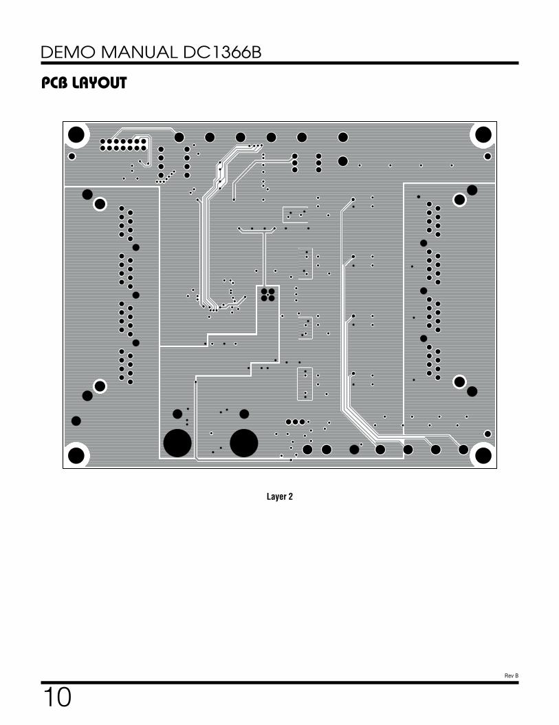
PCB LAYOUT
Bottom Assembly
ADI

14Rev B
DEMO MANUAL DC1366B
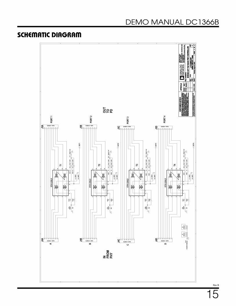
SCHEMATIC DIAGRAM5 5
4 4
3 3
2 2
1 1
DD
CC
BB
AA
ADDR
ESS
MSD
RESE
T
LO
VEE
+3.3
V
VEE
HI
MSD
DGND
SCL
SDAI
NIN
TSD
AOUT
SD1
SD2 SD
3 SD4
RTN
OUT1
OUT2
OUT3
OUT4
RECO
MMEN
DED
MINI
MUM
CABL
E SU
RGE
PRO
TECT
ION
RTN
-54V
RTN
RESE
T
DGND
MID
A1INT
A0
SD1
SENSE3
SENSE2
SENSE1SD4SD3
A2
SD2
RESET
AUTO
A3
MSD
AGND
_PIN
SENSE4GATE4
GATE3
GATE2
GATE1 GATE1
VDD
VDD
VDD
VDD
VEE
VEE
VEE
VEE
VEE
+3.3
V
VDD
VDD
VEE
SDAO
UTSD
AIN
SCL
AUTO
SD4
SD3
SD2
SD1
A1 A0USBV
DD
OUT1
OUT2
OUT3
OUT4
REVI
SION
HIS
TORY
DESC
RIPT
ION
DATE
APPR
OVED
ECO
REV
REBU
ILD
WIT
H CH
ANGE
208
-10-
15DI
LIAN
R.
REVI
SION
HIS
TORY
DESC
RIPT
ION
DATE
APPR
OVED
ECO
REV
REBU
ILD
WIT
H CH
ANGE
208
-10-
15DI
LIAN
R.
REVI
SION
HIS
TORY
DESC
RIPT
ION
DATE
APPR
OVED
ECO
REV
REBU
ILD
WIT
H CH
ANGE
208
-10-
15DI
LIAN
R.
SIZE
DATE
:
.VER.ON CI
SHEE
TOF
TITL
E:
APPR
OVAL
S
PCB
DES.
APP
ENG.
Fax:
(408
)434
-050
7
Milp
itas,
CA 95
035
Phon
e: (4
08)4
32-1
900
1630
McC
arth
y Blvd
.
LTC
Conf
iden
tial-F
or C
usto
mer
Use
Onl
y
CUST
OMER
NOT
ICE
LINE
AR T
ECHN
OLOG
Y HA
S MA
DE A
BES
T EF
FORT
TO
DESI
GN A
CIRC
UIT
THAT
MEE
TS C
USTO
MER-
SUPP
LIED
SPE
CIFI
CATI
ONS;
HOW
EVER
, IT R
EMAI
NS T
HE C
USTO
MER'
S RE
SPON
SIBI
LITY
TO
VERI
FY P
ROPE
R AN
D RE
LIAB
LE O
PERA
TION
IN T
HE A
CTUA
LAP
PLIC
ATIO
N. C
OMPO
NENT
SUB
STIT
UTIO
N AN
D PR
INTE
DCI
RCUI
T BO
ARD
LAYO
UT M
AY S
IGNI
FICA
NTLY
AFF
ECT
CIRC
UIT
PERF
ORMA
NCE
OR R
ELIA
BILI
TY. C
ONTA
CT L
INEA
RTE
CHNO
LOGY
APP
LICA
TION
S EN
GINE
ERIN
G FO
R AS
SIST
ANCE
.
THIS
CIR
CUIT
IS P
ROPR
IETA
RY T
O LI
NEAR
TEC
HNOL
OGY
AND
SCHE
MAT
IC
SUPP
LIED
FOR
USE
WIT
H LI
NEAR
TEC
HNOL
OGY
PART
S.SC
ALE
= NO
NE
www.
linea
r.com 2
LTC4
266C
UHF
13
IEEE
802.3
AT P
oE Q
UAD
PSE
CONT
ROLL
ER
KIM
T.
DILI
AN R
.
DEMO
CIR
CUIT
1366
BMo
nday
, Aug
ust 1
0, 20
15
N/A
SW7
TP2
D5 ORAN
GEVE
E
21
RS1B
1.00
RS3A
1.00
TP20
TP31
C47
0.22
uFX7
R
TP9
RS4B
1.00
Q2
PSM
N075
-100
MSE
2
4
731
6 85
SW4
D7 ORAN
GEVD
D
21
J2
+C2 10
uF10
0V
RS2A
1.00
D10
S1B
21
D6 RED
INT
21
JP2
HI LO
MID
SPAN
1 32
JP5
USB
VDD
EXT
VDD+3
.3V
SOUR
CE 1 32
12
D2SM
AJ5.
0A
D27
S1B
21
RS4C
1.00
C36
0.22
uFX7
R
TP17
G3
D9 S1B
21
C22
0.22
uFX7
R
TP1
RS3B
1.00
J1
12
D1SM
AJ58
A
TP5
TP8
RS2B
1.00
SW5
TP4
RS3C
1.00
RL1
300
R10 0
RS1A
1.00
D8 S1B
21
RS2C
1.00
R9 0OP
T
C64
1uF
100V
1206
1 2D2
8SM
BJ64
AOP
T
D26
S1B
21
RS4D
1.00
+C1
610
uF16
V
G1
TP16
RS1D
1.00
R11 0
Q3
PSM
N075
-100
MSE
2
4
731
6 85
TP6
TP7
SW2
TP19
RPW
130
0
TP3
D24
S1B
21
RS3D
1.00
D19
39V
13
SW3
Q4
PSM
N075
-100
MSE
2
4
731
6 85
RS2D
1.00
D11
S1B
21
RPW
23.
9K1/
4W
RS1C
1.00
D25
S1B
21
RS4A
1.00
JP4
HI LO
AUTO
1 32
R36
10 0805
C65
0.1u
F
D18
SMCJ
58A
21
G4
TP10
Q1
PSM
N075
-100
MSE
2
4
731
6 85
TP18
1 2
D23
SMAJ
5.0A
C66
4.7u
F12
06OP
T10
0V
C58
0.22
uFX7
R
R35
10 0805
SW1
1 2 3 4
8 7 6 5
G2
U1 LTC4
266
VEE 26
AGND 18
OUT 4 21
GATE 4 20SENSE 4 19
SENSE 3 22
GATE 3 23
OUT 3 24
SENSE 2 27
GATE 2 28
OUT 2 29
SENSE 1 30
GATE 1 31
OUT 1 32
VEE 25
DGND
10
AD0
7AD
16
AD2
5AD
34
SCL
38
SDAI
N3
SDAO
UT1
INT37
SD114
SD215
SD316
SD417
VDD13
AUTO33
MID36
RESET35
MSD34
VEE 39
SW6
15Rev B
DEMO MANUAL DC1366B
SCHEMATIC DIAGRAM5 5
4 4
3 3
2 2
1 1
DD
CC
BB
AA
IN FROM
PHY
OUT
TO PD
PORT
1
PORT
2
PORT
3
PORT
4
A B C D
J4J5
SHIE
LDSH
IELD
OUT1
OUT2
OUT3
OUT4
SIZE
DATE
:
.VER.ON CI
SHEE
TOF
TITL
E:
APPR
OVAL
S
PCB
DES.
APP
ENG.
Fax:
(408
)434
-050
7
Milp
itas,
CA 95
035
Phon
e: (4
08)4
32-1
900
1630
McC
arth
y Blvd
.
LTC
Conf
iden
tial-F
or C
usto
mer
Use
Onl
y
CUST
OMER
NOT
ICE
LINE
AR T
ECHN
OLOG
Y HA
S MA
DE A
BES
T EF
FORT
TO
DESI
GN A
CIRC
UIT
THAT
MEE
TS C
USTO
MER-
SUPP
LIED
SPE
CIFI
CATI
ONS;
HOW
EVER
, IT R
EMAI
NS T
HE C
USTO
MER'
S RE
SPON
SIBI
LITY
TO
VERI
FY P
ROPE
R AN
D RE
LIAB
LE O
PERA
TION
IN T
HE A
CTUA
LAP
PLIC
ATIO
N. C
OMPO
NENT
SUB
STIT
UTIO
N AN
D PR
INTE
DCI
RCUI
T BO
ARD
LAYO
UT M
AY S
IGNI
FICA
NTLY
AFF
ECT
CIRC
UIT
PERF
ORMA
NCE
OR R
ELIA
BILI
TY. C
ONTA
CT L
INEA
RTE
CHNO
LOGY
APP
LICA
TION
S EN
GINE
ERIN
G FO
R AS
SIST
ANCE
.
THIS
CIR
CUIT
IS P
ROPR
IETA
RY T
O LI
NEAR
TEC
HNOL
OGY
AND
SCHE
MAT
IC
SUPP
LIED
FOR
USE
WIT
H LI
NEAR
TEC
HNOL
OGY
PART
S.SC
ALE
= NO
NE
www.
linea
r.com 2
LTC4
266C
UHF
23
IEEE
802.3
AT P
oE Q
UAD
PSE
CONT
ROLL
ER
KIM
T.
DILI
AN R
.
DEMO
CIR
CUIT
1366
BMo
nday
, Aug
ust 1
0, 20
15
N/A
C52
0.01
uF20
0V
L8BE
AD
L3BE
AD
RJ45 - 4 PORTSJ4B 12345 678
T2
ETH1
-230
LD6
4
5
11
109
2
3
1
12
13 14
L1BE
AD
C38
0.01
uF20
0V
RJ45 - 4 PORTSJ4A 12345 678
C40
1000
pF
2kV
TP15
CHAS
SIS
GND
RJ45 - 4 PORTSJ4C 12345 678
C27
0.01
uF20
0V
R3N1
75
L5BE
AD
R1P1
75
R3N2 75
R2P2 75
C56
0.01
uF20
0V
R2N1
75
C45
0.01
uF20
0V
RJ45 - 4 PORTS
J5C
12345 678
RJ45 - 4 PORTSJ4D 12345 678
R2N2 75
C19
1000
pF
2kV
C49
1000
pF
2kV
R1P2 75
L4BE
AD
T3
ETH1
-230
LD6
4
5
11
109
2
3
1
12
13 14
C31
0.01
uF20
0V
R4P1
75
C20
0.01
uF20
0V
L2BE
AD
R4N2 75
R2P1
75
L6BE
AD
R4P2 75
RJ45 - 4 PORTS
J5D
12345 678
RJ45 - 4 PORTS
J5B
12345 678
T4
ETH1
-230
LD6
4
5
11
109
2
3
1
12
13 14
R1N1
75
C17
1000
pF2k
V
R3P1
75
T1
ETH1
-230
LD6
4
5
11
109
2
3
1
12
13 14
C42
1000
pF2k
V
RJ45 - 4 PORTS
J5A
12345 678
L7BE
AD
R4N1
75
R3P2 75
C34
1000
pF
2kV
C53
1000
pF2k
V
C28
1000
pF2k
V
R1N2 75
C60
0.01
uF20
0V

16Rev B
DEMO MANUAL DC1366B
SCHEMATIC DIAGRAM5 5
4 4
3 3
2 2
1 1
DD
CC
BB
AA
QUIC
KEVA
L FO
R DE
MO O
NLY
DEMO
PUR
POSE
S ON
LY
OPTI
ONAL
LED
DRI
VE
VDD
VDDP
VDDP
VDDP
VDDP
AUTO SD
3SD
4
SD2
SD1
A1 A0
SDAO
UT
SDAI
N
SCL
USBV
DD
OUT4
OUT3
OUT2
OUT1
SIZE
DATE
:
.VER.ON CI
SHEE
TOF
TITL
E:
APPR
OVAL
S
PCB
DES.
APP
ENG.
Fax:
(408
)434
-050
7
Milp
itas,
CA 95
035
Phon
e: (4
08)4
32-1
900
1630
McC
arth
y Blvd
.
LTC
Conf
iden
tial-F
or C
usto
mer
Use
Onl
y
CUST
OMER
NOT
ICE
LINE
AR T
ECHN
OLOG
Y HA
S MA
DE A
BES
T EF
FORT
TO
DESI
GN A
CIRC
UIT
THAT
MEE
TS C
USTO
MER-
SUPP
LIED
SPE
CIFI
CATI
ONS;
HOW
EVER
, IT R
EMAI
NS T
HE C
USTO
MER'
S RE
SPON
SIBI
LITY
TO
VERI
FY P
ROPE
R AN
D RE
LIAB
LE O
PERA
TION
IN T
HE A
CTUA
LAP
PLIC
ATIO
N. C
OMPO
NENT
SUB
STIT
UTIO
N AN
D PR
INTE
DCI
RCUI
T BO
ARD
LAYO
UT M
AY S
IGNI
FICA
NTLY
AFF
ECT
CIRC
UIT
PERF
ORMA
NCE
OR R
ELIA
BILI
TY. C
ONTA
CT L
INEA
RTE
CHNO
LOGY
APP
LICA
TION
S EN
GINE
ERIN
G FO
R AS
SIST
ANCE
.
THIS
CIR
CUIT
IS P
ROPR
IETA
RY T
O LI
NEAR
TEC
HNOL
OGY
AND
SCHE
MAT
IC
SUPP
LIED
FOR
USE
WIT
H LI
NEAR
TEC
HNOL
OGY
PART
S.SC
ALE
= NO
NE
www.
linea
r.com 2
LTC4
266C
UHF
33
IEEE
802.3
AT P
oE Q
UAD
PSE
CONT
ROLL
ER
KIM
T.
DILI
AN R
.
DEMO
CIR
CUIT
1366
BMo
nday
, Aug
ust 1
0, 20
15
N/A
D14
GREE
N
OUT3
21
R7 18M
R18
300
R6 1.1M 1%
D12
GREE
N
OUT1
21
R24
300
Q10
Si23
43DS
1
23
RX1
OPT
U324
LC02
5 A01
A12
A23
VSS
4
VCC
8
WP
7
SCL
6
SDA
5
TP29
D15
GREE
N
OUT4
21
RX6
OPT
REP1
5.1K
R16
1.1M 1%
R17
18M
J61 3
2 45
67
89
1011 13
12 14
REP2
5.1K
C4 0.1u
F
Q9Si
2343
DS
1
23
RX5
OPTR8 30
0
D13
GREE
N
OUT2
21
R21
300
J7OP
T 2 4 6 8 10 12 14 16
1 3 5 7 9 11 13 15
Q12
Si23
43DS
1
23
R23
18M
Q11
Si23
43DS
1
23
R22
1.1M 1%
R20
18M
RX4
OPT
R19
1.1M 1%
REP3
5.1K
RX3
OPT
RX2
OPT

17Rev B
DEMO MANUAL DC1366B
Information furnished by Analog Devices is believed to be accurate and reliable. However, no responsibility is assumed by Analog Devices for its use, nor for any infringements of patents or other rights of third parties that may result from its use. Specifications subject to change without notice. No license is granted by implication or otherwise under any patent or patent rights of Analog Devices.
REVISION HISTORYREV DATE DESCRIPTION PAGE NUMBER
A 12/15 Replaced Q1-Q4 with NXP PSMN075-100MSE, LFPAK33 package.Replaced SDAIN/SDAOUT jumper, JP3, tie option with resistor shunt R11.Changed diode D18 to SMCJ58A, 58V TVS.Removed 3.3V LDO, U2.Added AGND pin surge protection 10Ω resistor R35, moved logic pull-ups to VDD pin.Added VDD pin surge protection 10Ω resistor R36.Added SMAJ5.0A, 5V TVS, D2, across LTC4266 VDD and DGND pins.Changed diode D23 to SMAJ5.0A, 5V TVS.Renamed board logic ground to DGND, moved logic ground connections to DGND.Renamed VEE high side supply connection to RTN.Added R10, VDD pin shunt to AGND pin, and R9, DGND pin shunt option to AGND pin.Moved LED pull-up to +3.3V.
B 11/18 Ethernet Alliance certification logo added. 1

18Rev B
DEMO MANUAL DC1366B
© ANALOG DEVICES, INC. 2015 - 2018
11/18www.analog.com
ESD Caution ESD (electrostatic discharge) sensitive device. Charged devices and circuit boards can discharge without detection. Although this product features patented or proprietary protection circuitry, damage may occur on devices subjected to high energy ESD. Therefore, proper ESD precautions should be taken to avoid performance degradation or loss of functionality.
Legal Terms and Conditions By using the evaluation board discussed herein (together with any tools, components documentation or support materials, the “Evaluation Board”), you are agreeing to be bound by the terms and conditions set forth below (“Agreement”) unless you have purchased the Evaluation Board, in which case the Analog Devices Standard Terms and Conditions of Sale shall govern. Do not use the Evaluation Board until you have read and agreed to the Agreement. Your use of the Evaluation Board shall signify your acceptance of the Agreement. This Agreement is made by and between you (“Customer”) and Analog Devices, Inc. (“ADI”), with its principal place of business at One Technology Way, Norwood, MA 02062, USA. Subject to the terms and conditions of the Agreement, ADI hereby grants to Customer a free, limited, personal, temporary, non-exclusive, non-sublicensable, non-transferable license to use the Evaluation Board FOR EVALUATION PURPOSES ONLY. Customer understands and agrees that the Evaluation Board is provided for the sole and exclusive purpose referenced above, and agrees not to use the Evaluation Board for any other purpose. Furthermore, the license granted is expressly made subject to the following additional limitations: Customer shall not (i) rent, lease, display, sell, transfer, assign, sublicense, or distribute the Evaluation Board; and (ii) permit any Third Party to access the Evaluation Board. As used herein, the term “Third Party” includes any entity other than ADI, Customer, their employees, affiliates and in-house consultants. The Evaluation Board is NOT sold to Customer; all rights not expressly granted herein, including ownership of the Evaluation Board, are reserved by ADI. CONFIDENTIALITY. This Agreement and the Evaluation Board shall all be considered the confidential and proprietary information of ADI. Customer may not disclose or transfer any portion of the Evaluation Board to any other party for any reason. Upon discontinuation of use of the Evaluation Board or termination of this Agreement, Customer agrees to promptly return the Evaluation Board to ADI. ADDITIONAL RESTRICTIONS. Customer may not disassemble, decompile or reverse engineer chips on the Evaluation Board. Customer shall inform ADI of any occurred damages or any modifications or alterations it makes to the Evaluation Board, including but not limited to soldering or any other activity that affects the material content of the Evaluation Board. Modifications to the Evaluation Board must comply with applicable law, including but not limited to the RoHS Directive. TERMINATION. ADI may terminate this Agreement at any time upon giving written notice to Customer. Customer agrees to return to ADI the Evaluation Board at that time. LIMITATION OF LIABILITY. THE EVALUATION BOARD PROVIDED HEREUNDER IS PROVIDED “AS IS” AND ADI MAKES NO WARRANTIES OR REPRESENTATIONS OF ANY KIND WITH RESPECT TO IT. ADI SPECIFICALLY DISCLAIMS ANY REPRESENTATIONS, ENDORSEMENTS, GUARANTEES, OR WARRANTIES, EXPRESS OR IMPLIED, RELATED TO THE EVALUATION BOARD INCLUDING, BUT NOT LIMITED TO, THE IMPLIED WARRANTY OF MERCHANTABILITY, TITLE, FITNESS FOR A PARTICULAR PURPOSE OR NONINFRINGEMENT OF INTELLECTUAL PROPERTY RIGHTS. IN NO EVENT WILL ADI AND ITS LICENSORS BE LIABLE FOR ANY INCIDENTAL, SPECIAL, INDIRECT, OR CONSEQUENTIAL DAMAGES RESULTING FROM CUSTOMER’S POSSESSION OR USE OF THE EVALUATION BOARD, INCLUDING BUT NOT LIMITED TO LOST PROFITS, DELAY COSTS, LABOR COSTS OR LOSS OF GOODWILL. ADI’S TOTAL LIABILITY FROM ANY AND ALL CAUSES SHALL BE LIMITED TO THE AMOUNT OF ONE HUNDRED US DOLLARS ($100.00). EXPORT. Customer agrees that it will not directly or indirectly export the Evaluation Board to another country, and that it will comply with all applicable United States federal laws and regulations relating to exports. GOVERNING LAW. This Agreement shall be governed by and construed in accordance with the substantive laws of the Commonwealth of Massachusetts (excluding conflict of law rules). Any legal action regarding this Agreement will be heard in the state or federal courts having jurisdiction in Suffolk County, Massachusetts, and Customer hereby submits to the personal jurisdiction and venue of such courts. The United Nations Convention on Contracts for the International Sale of Goods shall not apply to this Agreement and is expressly disclaimed.