DEMO CIRCUIT 1288 QUICK START GUIDE LT3496EUFD Triple ... · Demonstration circuit 1288 is a Triple...
4
LT3496EUFD 1 DESCRIPTION WARNING! Do not look directly at operating LED. This circuit produces light that can damage eyes. Demonstration circuit 1288 is a Triple Boost or Buck-Boost LED Driver featuring the LT3496EUFD. The LT3496 is a triple output DC/DC converter designed to operate as current sources for driving high current LEDs. For evaluating an LT3496 buck mode LED driver, use the demonstration circuit 986. The board can be configured into either buck- boost (default) or boost mode. The current for each output is set at 200mA in either mode. The targeted input voltage PVIN range is 8V to 16V. The buck-boost circuit can tolerate an input voltage up to 40V when the LED string is on the high side. The part shuts down when the over- voltage threshold is reached. For a typical application with 5 LEDs totaling of 16V LED voltage, the circuit will operate until PVIN reaches 22V if the over-voltage protection is set to 38V. The buck-boost circuit with LEDs on the low side may not survive a 40V input transient. Applications with different input voltages and load combinations can be demonstrated on this circuit with some board modifications. Call the LTC applications group for support. Each of the three regulators on the demo board is independently operated. The PWM dimming feature of the LT3496 allows True Color PWM dimming with the dimming ratio of 5000:1. Additional analog dimming is possible. Setting CTRL voltage to be less than 1V will set the current sense voltage to be one-tenth of CTRL voltage, therefore, reduce the LED current. The output current should not exceed the rated current of the LEDs used. The LED current thermal de-rating should be considered to protect the LEDs. Adjustable switching frequency allows optimization of the efficiency and the external component size. The LT3496 datasheet gives complete description of the part, operation and application information. The datasheet must be read in conjunction with this quick start guide for working on or modifying the demo circuit 986. Design files for this circuit board are available. Call the LTC factory. , LTC and LT are registered trademarks of Linear Technology Corporation. DEMO CIRCUIT 1288 QUICK START GUIDE LT3496EUFD Triple Boost or Buck-Boost LED Driver
Transcript of DEMO CIRCUIT 1288 QUICK START GUIDE LT3496EUFD Triple ... · Demonstration circuit 1288 is a Triple...

LT3496EUFD
1
DESCRIPTION
WARNING!
Do not look directly at operating LED. This circuit produces light that can damage
eyes.
Demonstration circuit 1288 is a Triple Boost or Buck-Boost LED Driver featuring the LT3496EUFD. The LT3496 is a triple output DC/DC converter designed to operate as current sources for driving high current LEDs. For evaluating an LT3496 buck mode LED driver, use the demonstration circuit 986.
The board can be configured into either buck-boost (default) or boost mode. The current for each output is set at 200mA in either mode. The targeted input voltage PVIN range is 8V to 16V. The buck-boost circuit can tolerate an input voltage up to 40V when the LED string is on the high side. The part shuts down when the over-voltage threshold is reached. For a typical application with 5 LEDs totaling of 16V LED voltage, the circuit will operate until PVIN reaches 22V if the over-voltage protection is set to 38V. The buck-boost circuit with LEDs on the low side may not survive a 40V input transient. Applications with different input voltages and
load combinations can be demonstrated on this circuit with some board modifications. Call the LTC applications group for support.
Each of the three regulators on the demo board is independently operated. The PWM dimming feature of the LT3496 allows True Color PWM dimming with the dimming ratio of 5000:1. Additional analog dimming is possible.
Setting CTRL voltage to be less than 1V will set the current sense voltage to be one-tenth of CTRL voltage, therefore, reduce the LED current. The output current should not exceed the rated current of the LEDs used. The LED current thermal de-rating should be considered to protect the LEDs. Adjustable switching frequency allows optimization of the efficiency and the external component size.
The LT3496 datasheet gives complete description of the part, operation and application information. The datasheet must be read in conjunction with this quick start guide for working on or modifying the demo circuit 986.
Design files for this circuit board are available. Call the LTC factory.
, LTC and LT are registered trademarks of Linear Technology Corporation.
DEMO CIRCUIT 1288QUICK START GUIDE
LT3496EUFDTriple Boost or Buck-Boost
LED Driver
LT3496EUFD
2
* VLED is the forward voltage drop of a LED string ** VIN of the demo board is limited by the choice of the input capacitor. The LT3496 input range is 3V-30V with transient protection to 40V. A lower VIN helps to reduce the power dissipation in the chip. MODE SETUP JP3, JP4, JP5 C2, C6, C8 C11, C12, C13 LED on High Side LED on Low Side Buck-Boost =Buck-Boost Not Install Install Short LEDnL+ and
LEDnL- Short LEDnH+ and LEDnH-
Boost =Boost Install Not Install N/A Short LEDnH+ and LEDnH-
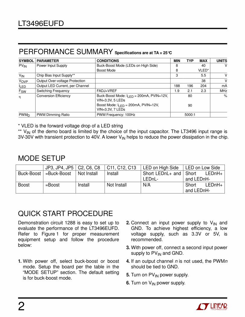
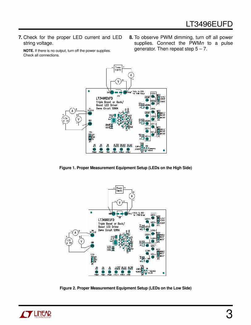
QUICK START PROCEDURE Demonstration circuit 1288 is easy to set up to evaluate the performance of the LT3496EUFD. Refer to Figure 1 for proper measurement equipment setup and follow the procedure below:
1. With power off, select buck-boost or boost mode. Setup the board per the table in the “MODE SETUP” section. The default setting is for buck-boost mode.
2. Connect an input power supply to VIN and GND. To achieve highest efficiency, a low voltage supply, such as 3.3V or 5V, is recommended.
3. With power off, connect a second input power supply to PVIN and GND.
4. If an output channel n is not used, the PWMn should be tied to GND.
5. Turn on PVIN power supply.
6. Turn on VIN power supply.
PERFORMANCE SUMMARY Specifications are at TA = 25°C
SYMBOL PARAMETER CONDITIONS MIN TYP MAX UNITSPVIN Power Input Supply Buck-Boost Mode (LEDs on High Side)
Boost Mode 8 8
40 VLED*
V
VIN Chip Bias Input Supply** 3 5.5 VVOVP Output Over-voltage Protection 38 VILED Output LED Current, per Channel 188 196 204 mAFSW Switching Frequency FADJ=VREF 1.9 2.1 2.3 MHz
η Conversion Efficiency Buck-Boost Mode: ILED = 200mA, PVIN=12V, VIN=3.3V, 5 LEDs Boost Mode: ILED = 200mA, PVIN=12V, VIN=3.3V, 7 LEDs
80
90
%
PWMD PWM Dimming Ratio PWM Frequency: 100Hz 5000:1
LT3496EUFD
3
7. Check for the proper LED current and LED string voltage. NOTE. If there is no output, turn off the power supplies. Check all connections.
8. To observe PWM dimming, turn off all power supplies. Connect the PWMn to a pulse generator. Then repeat step 5 – 7.
Figure 1. Proper Measurement Equipment Setup (LEDs on the High Side)
Figure 2. Proper Measurement Equipment Setup (LEDs on the Low Side)
LT3496EUFD
4