DECEMBER 2011 60-V,5-µA IQ, 100-mA,Low...
20
TPS7A16xx OUT GND C IN IN EN V IN V OUT V EN R PG DELAY C DELAY PG C OUT V PG mC1 IO1 IO2 IO3 mC2 EN VCC 12 V 60 V t V IN 2 1 3 4 7 8 6 5 FB/DNC PG GND OUT EN NC DELAY IN DGN PACKAGE 3mm 5mm MSOP-8 PowerPAD (TOP VIEW) ´ TPS7A16 www.ti.com SBVS171A – DECEMBER 2011 – REVISED DECEMBER 2011 60-V, 5-µAI Q , 100-mA, Low-Dropout VOLTAGE REGULATOR with Enable and Power-Good Check for Samples: TPS7A16 1FEATURES DESCRIPTION The TPS7A16 family of ultra-low power, low-dropout 23• Wide Input Voltage Range: 3 V to 60 V (LDO) voltage regulators offers the benefits of • Ultralow Quiescent Current: 5 µA ultra-low quiescent current, high input voltage and • Quiescent Current at Shutdown: 1 µA miniaturized, high thermal-performance packaging. • Output Current: 100 mA The TPS7A16 family is designed for continuous or • Low Dropout Voltage: 60 mV at 20 mA sporadic (power backup) battery-powered applications where ultra-low quiescent current is • Accuracy: 2% critical to extending system battery life. • Available in: The TPS7A16 family offers an enable pin (EN) – Fixed Output Voltage: 3.3 V, 5.0 V compatible with standard CMOS logic and an – Adjustable Version from ~1.2 V to 18.5 V integrated open drain active-high power good output • Power Good with Programable Delay (PG) with a user-programmable delay. These pins are intended for use in microcontroller-based, • Current-Limit and Thermal Shutdown battery-powered applications where power-rail Protections sequencing is required. • Stable with Ceramic Output Capactors: In addition, the TPS7A16 is ideal for generating a ≥ 2.2 µF low-voltage supply from multicell solutions ranging • Package: High Thermal Performance MSOP-8 from high cell-count power-tool packs to automotive PowerPAD™ applications; not only can this device supply a • Operating Temperature Range: well-regulated voltage rail, but it can also withstand –40°C to +125°C and maintain regulation during voltage transients. These features translate to simpler and more cost-effective, electrical surge-protection circuitry. APPLICATIONS • High Cell-Count Battery Packs for Power Tools and other Battery-Powered Microprocessor and Microcontroller Systems • Car Audio, Navigation, Infotainment, and Other Automotive Systems • Power Supplies for Notebook PCs, Digital TVs, and Private LAN Systems • Smoke/CO 2 Detectors and Battery-Powered Alarm/Security Systems Low Power Microcontroller Rail Sequencing in Automotive Applications Subject to Load Dump Transient 1 Please be aware that an important notice concerning availability, standard warranty, and use in critical applications of Texas Instruments semiconductor products and disclaimers thereto appears at the end of this data sheet. 2PowerPAD is a trademark of Texas Instruments. 3All other trademarks are the property of their respective owners. PRODUCTION DATA information is current as of publication date. Copyright © 2011, Texas Instruments Incorporated Products conform to specifications per the terms of the Texas Instruments standard warranty. Production processing does not necessarily include testing of all parameters.
Transcript of DECEMBER 2011 60-V,5-µA IQ, 100-mA,Low...

TPS7A16xx
OUT
GND
CIN
IN
EN
VIN
VOUT
VEN
RPG
DELAY
CDELAY
PG
COUT
VPG
mC1
IO1
IO2
IO3
mC2
EN
VCC
12 V
60 V
t
VIN
2
1
3
4
7
8
6
5
FB/DNC
PG
GND
OUT
EN
NC
DELAY
IN
DGN PACKAGE
3mm 5mm MSOP-8 PowerPAD
(TOP VIEW)
´
TPS7A16
www.ti.com SBVS171A –DECEMBER 2011–REVISED DECEMBER 2011
60-V, 5-µA IQ, 100-mA, Low-Dropout VOLTAGE REGULATORwith Enable and Power-Good
Check for Samples: TPS7A16
1FEATURES DESCRIPTIONThe TPS7A16 family of ultra-low power, low-dropout
23• Wide Input Voltage Range: 3 V to 60 V(LDO) voltage regulators offers the benefits of• Ultralow Quiescent Current: 5 µA ultra-low quiescent current, high input voltage and
• Quiescent Current at Shutdown: 1 µA miniaturized, high thermal-performance packaging.• Output Current: 100 mA The TPS7A16 family is designed for continuous or• Low Dropout Voltage: 60 mV at 20 mA sporadic (power backup) battery-powered
applications where ultra-low quiescent current is• Accuracy: 2%critical to extending system battery life.• Available in:The TPS7A16 family offers an enable pin (EN)– Fixed Output Voltage: 3.3 V, 5.0 Vcompatible with standard CMOS logic and an
– Adjustable Version from ~1.2 V to 18.5 V integrated open drain active-high power good output• Power Good with Programable Delay (PG) with a user-programmable delay. These pins are
intended for use in microcontroller-based,• Current-Limit and Thermal Shutdownbattery-powered applications where power-railProtectionssequencing is required.
• Stable with Ceramic Output Capactors:In addition, the TPS7A16 is ideal for generating a≥ 2.2 µFlow-voltage supply from multicell solutions ranging• Package: High Thermal Performance MSOP-8 from high cell-count power-tool packs to automotive
PowerPAD™ applications; not only can this device supply a• Operating Temperature Range: well-regulated voltage rail, but it can also withstand
–40°C to +125°C and maintain regulation during voltage transients.These features translate to simpler and morecost-effective, electrical surge-protection circuitry.APPLICATIONS
• High Cell-Count Battery Packs for Power Toolsand other Battery-Powered Microprocessorand Microcontroller Systems
• Car Audio, Navigation, Infotainment, and OtherAutomotive Systems
• Power Supplies for Notebook PCs, Digital TVs,and Private LAN Systems
• Smoke/CO2 Detectors and Battery-PoweredAlarm/Security Systems
Low Power Microcontroller Rail Sequencing inAutomotive Applications Subject to Load Dump
Transient
1
Please be aware that an important notice concerning availability, standard warranty, and use in critical applications of TexasInstruments semiconductor products and disclaimers thereto appears at the end of this data sheet.
2PowerPAD is a trademark of Texas Instruments.3All other trademarks are the property of their respective owners.
PRODUCTION DATA information is current as of publication date. Copyright © 2011, Texas Instruments IncorporatedProducts conform to specifications per the terms of the TexasInstruments standard warranty. Production processing does notnecessarily include testing of all parameters.

TPS7A16
SBVS171A –DECEMBER 2011–REVISED DECEMBER 2011 www.ti.com
This integrated circuit can be damaged by ESD. Texas Instruments recommends that all integrated circuits be handled withappropriate precautions. Failure to observe proper handling and installation procedures can cause damage.
ESD damage can range from subtle performance degradation to complete device failure. Precision integrated circuits may be moresusceptible to damage because very small parametric changes could cause the device not to meet its published specifications.
ORDERING INFORMATION (1)
PRODUCT VOUT
TPS7A16xx yyy z XX is nominal output voltage ( 01 = Adjustable, 33 = 3.3 V, 50 = 5.0 V) (2)
YYY is package designator.Z is package quantity.
(1) For the most current package and ordering information see the Package Option Addendum at the end of this document, or visit thedevice product folder on www.ti.com.
(2) Additional output voltage options are available. Minimum-order quantities may apply; contact your sales representative for details.
ABSOLUTE MAXIMUM RATINGS (1)
Over operating free-air temperature range –40°C ≤ TJ ≤ +125°C (unless otherwise noted).VALUE
MIN MAX UNIT
IN pin to GND pin –0.3 +62 V
OUT pin to GND pin –0.3 +20 V
OUT pin to IN pin –62 +0.3 V
FB pin to GND pin –0.3 +3 V
Voltage FB pin to IN pin –62 +0.3 V
EN pin to IN pin –62 0.3 V
EN pin to GND pin –0.3 +62 V
PG pin to GND pin –0.3 +5.5 V
DELAY pin to GND pin –0.3 +5.5 V
Current Peak output Internally limited
Operating virtual junction, TJ, absolute maximum range (2) –40 +150 °CTemperature
Storage, Tstg –65 +150 °C
Human body model (HBM) 2 kVElectrostatic discharge rating
Charged device model (CDM) 500 V
(1) Stresses beyond those listed under Absolute Maximum Ratings may cause permanent damage to the device. These are stress ratingsonly, and functional operation of the device at these or any other conditions beyond those indicated is not implied. Exposure toabsolute-maximum rated conditions for extended periods may affect device reliability.
(2) No permanent damage will occur to the part operating within this range though electrical performance is not guaranteed outside theoperating free-air temperature range.
THERMAL INFORMATIONTPS7A1601
THERMAL METRIC (1) DGN UNITS
8 PINS
θJA Junction-to-ambient thermal resistance 66.2
θJC(top) Junction-to-case(top) thermal resistance 45.9
θJB Junction-to-board thermal resistance 34.6°C/W
ψJT Junction-to-top characterization parameter 1.9
ψJB Junction-to-board characterization parameter 34.3
θJC(bottom) Junction-to-case(bottom) thermal resistance 14.9
(1) For more information about traditional and new thermal metrics, see the IC Package Thermal Metrics application report, SPRA953.
2 Submit Documentation Feedback Copyright © 2011, Texas Instruments Incorporated
Product Folder Link(s): TPS7A16

TPS7A16
www.ti.com SBVS171A –DECEMBER 2011–REVISED DECEMBER 2011
ELECTRICAL CHARACTERISTICSAt TJ = –40°C to +125°C, VIN = VOUT(NOM) + 0.5 V or VIN = 3.0 V (whichever is greater), VEN = VIN, IOUT = 10 µA, CIN = 1 μF, COUT = 2.2 μF,and FB tied to OUT, unless otherwise noted.
TPS7A1601
PARAMETER TEST CONDITIONS MIN TYP MAX UNIT
VIN Input voltage range 3 60 V
VREF Internal reference TJ = +25°C, VFB = VREF, VIN = 3 V, IOUT = 10 μA 1.169 1.193 1.217 V
VUVLO Undervoltage lockout threshold 2.7 V
Output voltage range VIN ≥ VOUT(NOM) + 0.5 V VREF 18.5 V
Nominal accuracy TJ = +25°C, VIN = 3 V, IOUT = 10 μA –2.0% +2.0% VOUTVOUTVOUT(NOM) + 0.5 V ≤ VIN ≤ 60 V (1)
Overall accuracy –2.0% +2.0% VOUT10 µA ≤ IOUT ≤ 100 mA
ΔVO(ΔVI) Line regulation 3 V ≤ VIN ≤ 60 V ±1.0% VOUT
ΔVO(ΔIO) Load regulation 10 µA ≤ IOUT ≤ 100 mA ±1.0% VOUT
VIN = 4.5 V, VOUT(NOM) = 5 V, IOUT = 20 mA 60 mVVDO Dropout voltage
VIN = 4.5 V, VOUT(NOM) = 5 V, IOUT = 100 mA 265 500 mV
ILIM Current limit VOUT = 90% VOUT(NOM), VIN = 3.0 V 101 225 400 mA
3 V ≤ VIN ≤ 60 V, IOUT = 10 µA 5.0 15 μAIGND Ground current
IOUT = 100 mA 5.0 μA
ISHDN Shutdown supply current VEN = +0.4 V 0.59 5.0 μA
I FB Feedback current (2) –1.0 0.0 1.0 µA
IEN Enable current 3 V ≤ VIN ≤ 12 V, VIN = VEN –1.0 0.01 1.0 μA
VEN_HI Enable high-level voltage 1.2 V
VEN_LO Enable low- level voltage 0.3 V
OUT pin floating, VFB increasing, VIN ≥ VIN_MIN 85% 95% VOUTVIT PG trip threshold
OUT pin floating, VFB decreasing, VIN ≥ VIN_MIN 83% 93% VOUT
VHYS PG trip hysteresis 2.3% 4% VOUT
VPG, LO PG output low voltage OUT pin floating, VFB = 80% VREF, IPG= 1mA 0.4 V
IPG, LKG PG leakage current VPG= VOUT(NOM) –1.0 1.0 μA
IDELAY DELAY pin current 1.0 2.0 μA
VIN = 3 V, VOUT(NOM) = VREF, COUT = 10 μF,PSRR Power-supply rejection ratio 50 dBf = 100 Hz
Shutdown, temperature increasing +170 °CTSD Thermal shutdown temperature
Reset, temperature decreasing +150 °COperating junction temperatureTJ –40 +125 °Crange
(1) Maximum input voltage is limited to 24 V because of the package power dissipation limitations at full load (P ≈ (VIN – VOUT) × IOUT =(24 V – VREF) × 50 mA ≈ 1.14 W). The device is capable of sourcing a maximum current of 50 mA at higher input voltages as long asthe power dissipated is within the thermal limits of the package plus any external heatsinking.
(2) IFB > 0 flows out of the device.
Copyright © 2011, Texas Instruments Incorporated Submit Documentation Feedback 3
Product Folder Link(s): TPS7A16

UVLO
ThermalShutdown
CurrentLimit
EnableErrorAmp
IN
EN
OUT
FB
PassDevice
PowerGood
Control
DELAY
PG
TPS7A1601
OUT
GND
CIN
IN
EN
VIN V
OUT
VEN
DELAY PG
COUT
FB
VPG
RPG
CFF
R1
R2
CDELAY
VOUT
VREF
- 1R = R1 2
Where:
TPS7A16
SBVS171A –DECEMBER 2011–REVISED DECEMBER 2011 www.ti.com
DEVICE INFORMATION
FUNCTIONAL BLOCK DIAGRAM
TYPICAL APPLICATION CIRCUIT
TPS7A1601 Circuit as an Adjustable Regulator
4 Submit Documentation Feedback Copyright © 2011, Texas Instruments Incorporated
Product Folder Link(s): TPS7A16

2
1
3
4
7
8
6
5
FB/DNC
PG
GND
OUT
EN
NC
DELAY
IN
TPS7A16
www.ti.com SBVS171A –DECEMBER 2011–REVISED DECEMBER 2011
PIN CONFIGURATION
DGN PACKAGEMSOP-8
(TOP VIEW)
PIN DESCRIPTIONSTPS7A16xx
NAME NO. DESCRIPTION
DELAY 7 Delay pin. Connect a capacitor to GND to adjust the PG delay time; leave open if the reset function is not needed.
Enable pin. This pin turns the regulator on or off.If VEN ≥ VEN_HI, the regulator is enabled.EN 5 If VEN ≤ VEN_LO, the regulator is disabled.If not used, the EN pin can be connected to IN. Make sure that VEN ≤ VIN at all times.
For the adjustable version (TPS7A1601), the feedback pin is the input to the control-loop error amplifier. This pin isused to set the output voltage of the device when the regulator output voltage is set by external resistors.FB/DNC 2 For the fixed voltage versions: DO NOT CONNECT to this pin. Do not route this pin to any electrical net, not evenGND or IN.
GND 4 Ground pin.
Regulator input supply pin. A capacitor > 0.1 µF must be tied from this pin to ground to assure stability. It isrecommended to connect a 10 µF ceramic capacitor from IN to GND (as close to the device as possible) to reduceIN 8 circuit sensitivity to printed-circuit-board (PCB) layout, especially when long input tracer or high source impedancesare encountered.
NC 6 This pin can be left open or tied to any voltage between GND and IN.
Regulator output pin. A capacitor > 2.2 µF must be tied from this pin to ground to assure stability. It is recommendedOUT 1 to connect a 10 µF ceramic capacitor from OUT to GND (as close to the device as possible) to maximize AC
performance.
PG 3 Power-good pin. Open collector output; leave open or connect to GND if the power-good function is not needed.
Solder to printed circuit board (PCB) to enhance thermal performance. Although it can be left floating, it is highlyPowerPAD recommended to connect the PowerPAD to the GND plane.
Copyright © 2011, Texas Instruments Incorporated Submit Documentation Feedback 5
Product Folder Link(s): TPS7A16
0
10
20
30
40
50
0 10 20 30 40 50 60Input Voltage (V)
I Q (
µA)
− 40°C+ 25°C+ 85°C+ 105°C+ 125°C
IOUT = 0mA
0
1
2
3
4
5
6
7
8
9
10
0 10 20 30 40 50 60Input Voltage (V)
I Q (
µA)
− 40°C+ 25°C+ 85°C+ 105°C+ 125°C
VEN = 0.4V
0
10
20
30
40
50
60
70
80
90
100
0 10 20 30 40 50 60 70 80 90 100Output Current (mA)
I GN
D (
µA)
− 40°C+ 25°C+ 85°C+ 105°C+ 125°C
0
100
200
300
400
500
600
700
800
900
1000
0 20 40 60 80 100Output Current (mA)
VD
RO
P (
V)
− 40°C+ 25°C+ 85°C
+ 105°C+ 125°C
1.094
1.144
1.194
1.244
1.294
0 10 20 30 40 50 60Input Voltage (V)
VF
B (
V)
− 40°C+ 25°C+ 85°C
+ 105°C+ 125°C
−10
−7.5
−5
−2.5
0
2.5
5
7.5
10
0 10 20 30 40 50 60Input Voltage (V)
VO
UT
(NO
M) (
%)
− 40°C+ 25°C+ 85°C
+ 105°C+ 125°C
TPS7A16
SBVS171A –DECEMBER 2011–REVISED DECEMBER 2011 www.ti.com
TYPICAL CHARACTERISTICSAt TJ = –40°C to +125°C, VIN = VOUT(NOM) + 0.5 V or VIN = 3.0 V (whichever is greater), VEN = VIN, IOUT = 10 µA, CIN = 1 μF,
COUT = 2.2 μF, and FB tied to OUT, unless otherwise noted.
QUIESCENT CURRENT vs INPUT VOLTAGE SHUTDOWN CURRENT vs INPUT VOLTAGE
Figure 1. Figure 2.
GROUND CURRENT vs OUTPUT CURRENT DROPOUT VOLTAGE vs OUTPUT CURRENT
Figure 3. Figure 4.
FEEDBACK VOLTAGE vs INPUT VOLTAGE LINE REGULATION
Figure 5. Figure 6.
6 Submit Documentation Feedback Copyright © 2011, Texas Instruments Incorporated
Product Folder Link(s): TPS7A16

−10
−7.5
−5
−2.5
0
2.5
5
7.5
10
0 10 20 30 40 50 60 70 80 90 100Output Current (mA)
VO
UT
(NO
M) (
%)
− 40°C+ 25°C+ 85°C
+ 105°C+ 125°C
0
50
100
150
200
250
300
0 2 4 6 8 10 12Input Voltage (V)
I CL (
mA
)
− 40°C+ 25°C+ 85°C+ 105°C+ 125°C
85
87
89
91
93
95
−40 −25 −10 5 20 35 50 65 80 95 110 125
PG Falling
PG Rising
Temperature (°C)
VO
UT
NO
M (
%)
0
0.5
1
1.5
2
2.5
−40 −25 −10 5 20 35 50 65 80 95 110 125
ON−TO−OFF
OFF−TO−ON
Temperature (°C)
VE
N (
V)
0
10
20
30
40
50
60
70
80
90
100
10 100 1k 10k 100kFrequency (Hz)
PS
RR
(dB
)
VIN = 3VVOUT = ~1.2VCOUT = 10µF
0.001
0.01
0.1
1
10
10 100 1k 10k 100k 1M 10MFrequency (Hz)
Noi
se (
µV/
Hz
)
VIN = 3VVOUT = 1.2VCOUT = 2.2µF
TPS7A16
www.ti.com SBVS171A –DECEMBER 2011–REVISED DECEMBER 2011
TYPICAL CHARACTERISTICS (continued)At TJ = –40°C to +125°C, VIN = VOUT(NOM) + 0.5 V or VIN = 3.0 V (whichever is greater), VEN = VIN, IOUT = 10 µA, CIN = 1 μF,COUT = 2.2 μF, and FB tied to OUT, unless otherwise noted.
LOAD REGULATION CURRENT LIMIT vs INPUT VOLTAGE
Figure 7. Figure 8.
POWER-GOOD THRESHOLD VOLTAGE vsTEMPERATURE ENABLE THRESHOLD VOLTAGE vs TEMPERATURE
Figure 9. Figure 10.
POWER-SUPPLY REJECTION RATIO OUTPUT SPECTRAL NOISE DENSITY
Figure 11. Figure 12.
Copyright © 2011, Texas Instruments Incorporated Submit Documentation Feedback 7
Product Folder Link(s): TPS7A16
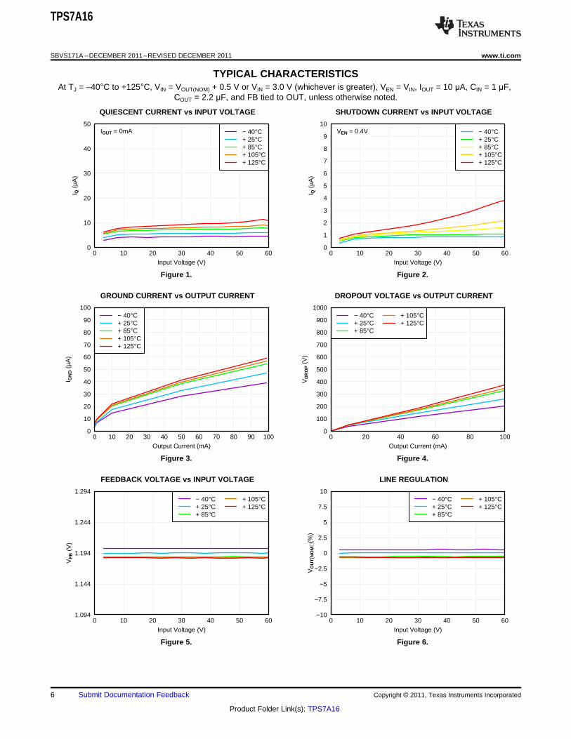
V = 1 V 6.5 V
I = 1 mA
®IN
OUT
C = 10 F
C = 0 nF
OUT
FF
m
Time (5 ms/div)
V (2 V/div)IN
V (2 V/div)PG
V (1 V/div)OUT
TPS7A16
SBVS171A –DECEMBER 2011–REVISED DECEMBER 2011 www.ti.com
TYPICAL CHARACTERISTICS (continued)At TJ = –40°C to +125°C, VIN = VOUT(NOM) + 0.5 V or VIN = 3.0 V (whichever is greater), VEN = VIN, IOUT = 10 µA, CIN = 1 μF,COUT = 2.2 μF, and FB tied to OUT, unless otherwise noted.
POWER GOOD DELAY
Figure 13.
8 Submit Documentation Feedback Copyright © 2011, Texas Instruments Incorporated
Product Folder Link(s): TPS7A16
IN
EN
DELAY
GND
C
0.1 Fm
IN
C
0.1 Fm
DELAY
VIN PG
OUT
FB
R
1.07 MW
2
R
3.4 MW
1
R
1 MW
PG
C
2.2 Fm
OUT
V
5 V
OUT
VOUT
VREF
- 1R = R1 2
TPS7A16
www.ti.com SBVS171A –DECEMBER 2011–REVISED DECEMBER 2011
THEORY OF OPERATION
GENERAL DESCRIPTION
The TPS7A16 family of ultra-low power voltage regulators offers the benefit of ultra-low quiescent current, highinput voltage, and miniaturized, high thermal-performance packaging.
The TPS7A16 family is designed for continuous or sporadic (power backup) battery-operated applications whereultra-low quiescent current is critical to extending system battery life.
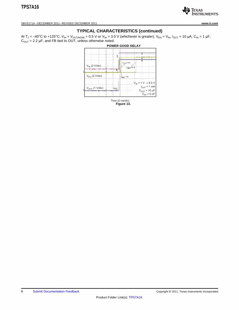
ADJUSTABLE VOLTAGE OPERATION
The TPS7A1601 has an output voltage range from 1.194 V to 20 V. The nominal output of the device is set bytwo external resistors, as shown in Figure 14:
Figure 14. Adjustable Operation
R1 and R2 can be calculated for any output voltage range using the formula shown in Equation 1:
(1)
Resistor Selection
It is recommended to use resistors in the order of MΩ to keep the overall quiescent current of the system as lowas possible (by making the current used by the resistor divider negligible compared to the device’s quiescentcurrent).
If greater voltage accuracy is required, take into account the voltage offset contributions as a result of feedbackcurrent and use of 0.1% tolerance resistors.
Table 1 shows the resistor combination to achieve a few of the most common rails using commercially available0.1% tolerance resistors to maximize nominal voltage accuracy, while abiding to the formula shown inEquation 1.
Copyright © 2011, Texas Instruments Incorporated Submit Documentation Feedback 9
Product Folder Link(s): TPS7A16
TPS7A16
SBVS171A –DECEMBER 2011–REVISED DECEMBER 2011 www.ti.com
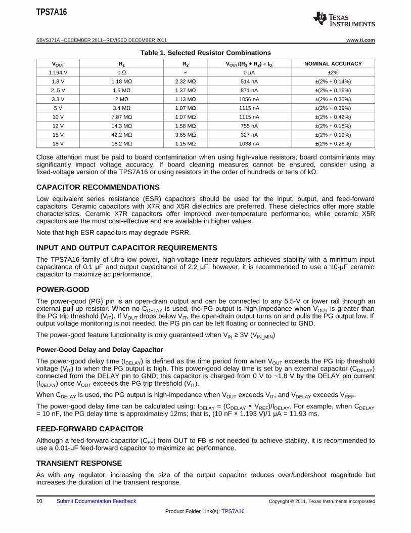
Table 1. Selected Resistor Combinations
VOUT R1 R2 VOUT/(R1 + R2) « IQ NOMINAL ACCURACY
1.194 V 0 Ω ∞ 0 µA ±2%
1.8 V 1.18 MΩ 2.32 MΩ 514 nA ±(2% + 0.14%)
2..5 V 1.5 MΩ 1.37 MΩ 871 nA ±(2% + 0.16%)
3.3 V 2 MΩ 1.13 MΩ 1056 nA ±(2% + 0.35%)
5 V 3.4 MΩ 1.07 MΩ 1115 nA ±(2% + 0.39%)
10 V 7.87 MΩ 1.07 MΩ 1115 nA ±(2% + 0.42%)
12 V 14.3 MΩ 1.58 MΩ 755 nA ±(2% + 0.18%)
15 V 42.2 MΩ 3.65 MΩ 327 nA ±(2% + 0.19%)
18 V 16.2 MΩ 1.15 MΩ 1038 nA ±(2% + 0.26%)
Close attention must be paid to board contamination when using high-value resistors; board contaminants maysignificantly impact voltage accuracy. If board cleaning measures cannot be ensured, consider using afixed-voltage version of the TPS7A16 or using resistors in the order of hundreds or tens of kΩ.
CAPACITOR RECOMMENDATIONS
Low equivalent series resistance (ESR) capacitors should be used for the input, output, and feed-forwardcapacitors. Ceramic capacitors with X7R and X5R dielectrics are preferred. These dielectrics offer more stablecharacteristics. Ceramic X7R capacitors offer improved over-temperature performance, while ceramic X5Rcapacitors are the most cost-effective and are available in higher values.
Note that high ESR capacitors may degrade PSRR.
INPUT AND OUTPUT CAPACITOR REQUIREMENTS
The TPS7A16 family of ultra-low power, high-voltage linear regulators achieves stability with a minimum inputcapacitance of 0.1 µF and output capacitance of 2.2 µF; however, it is recommended to use a 10-µF ceramiccapacitor to maximize ac performance.
POWER-GOOD
The power-good (PG) pin is an open-drain output and can be connected to any 5.5-V or lower rail through anexternal pull-up resistor. When no CDELAY is used, the PG output is high-impedance when VOUT is greater thanthe PG trip threshold (VIT). If VOUT drops below VIT, the open-drain output turns on and pulls the PG output low. Ifoutput voltage monitoring is not needed, the PG pin can be left floating or connected to GND.
The power-good feature functionality is only guaranteed when VIN ≥ 3V (VIN_MIN)
Power-Good Delay and Delay Capacitor
The power-good delay time (tDELAY) is defined as the time period from when VOUT exceeds the PG trip thresholdvoltage (VIT) to when the PG output is high. This power-good delay time is set by an external capacitor (CDELAY)connected from the DELAY pin to GND; this capacitor is charged from 0 V to ~1.8 V by the DELAY pin current(IDELAY) once VOUT exceeds the PG trip threshold (VIT).
When CDELAY is used, the PG output is high-impedance when VOUT exceeds VIT, and VDELAY exceeds VREF.
The power-good delay time can be calculated using: tDELAY = (CDELAY × VREF)/IDELAY. For example, when CDELAY= 10 nF, the PG delay time is approximately 12ms; that is, (10 nF × 1.193 V)/1 µA = 11.93 ms.
FEED-FORWARD CAPACITOR
Although a feed-forward capacitor (CFF) from OUT to FB is not needed to achieve stability, it is recommended touse a 0.01-µF feed-forward capacitor to maximize ac performance.
TRANSIENT RESPONSE
As with any regulator, increasing the size of the output capacitor reduces over/undershoot magnitude butincreases the duration of the transient response.
10 Submit Documentation Feedback Copyright © 2011, Texas Instruments Incorporated
Product Folder Link(s): TPS7A16

TPS7A16xx
OUT
GND
CIN
IN
EN
VIN
VOUT
VEN
RPG
DELAY
CDELAY
PG
COUT
VPG
mC1
IO1
IO2
IO3
mC2
EN
VCC
12 V
60 V
t
VIN
TPS7A16
www.ti.com SBVS171A –DECEMBER 2011–REVISED DECEMBER 2011
APPLICATION INFORMATION
AUTOMOTIVE APPLICATIONS
The TPS7A16 family maximum input voltage of 60 V makes it ideal for use in automotive applications wherehigh-voltage transients are present.
Events such as load-dump overvoltage (where the battery is disconnected while the alternator is providingcurrent to a load) may cause voltage spikes from 25 V to 60 V. In order to prevent any damage to sensitivecircuitry, local transient voltage suppressors can be used to cap voltage spikes to lower, more manageablevoltages.
The TPS7A16 family can be used to simplify and lower costs in such cases. The TPS7A16 very high voltagerange allows this regulator to not only withstand the voltages coming out of these local transient voltagesuppressors, but even replace them, thus lowering system cost and complexity.
Figure 15. Low-Power Microcontroller Rail Sequencing in Automotive Applications Subjected toLoad-Dump Transients
MULTICELL BATTERY PACKS
Currently, battery packs can employ up to a dozen cells in series that, when fully charged, may have voltages ofup to 55 V. Internal circuitry in these battery packs is used to prevent overcurrent and overvoltage conditions thatmay degrade battery life or even pose a safety risk; this internal circuitry is often managed by a low-powermicrocontroller, such as TI’s MSP430.
The microcontroller continuously monitors the battery itself, whether the battery is in use or not. Although thismicrocontroller could be powered by an intermediate voltage taken from the multicell array, this approachunbalances the battery pack itself, degrading its life or adding cost to implement more complex cell balancingtopologies.
The best approach to power this microcontroller is to regulate down the voltage from the entire array to dischargeevery cell equally and prevent any balancing issues. This approach reduces system complexity and cost.
TPS7A16 is the ideal regulator for this application because it can handle very high voltages (from the entiremulticell array) and has very low quiescent current (to maximize battery life).
Copyright © 2011, Texas Instruments Incorporated Submit Documentation Feedback 11
Product Folder Link(s): TPS7A16

CellBalance
VoltageSensing
TPS7A16
Comparator
Microcontroller
Sensing
+
-
UART
Up To 42 V
100 W
0.47 FmOptionalFilter
FirstCell
LastCell
SecondCell
LDO
MSP430
Microcontroller
PWM
Transient
M
TPS7A16
SBVS171A –DECEMBER 2011–REVISED DECEMBER 2011 www.ti.com
Figure 16. Protection Based on Low-Power Microcontroller Power from Multicell Battery Packs
BATTERY-OPERATED POWER TOOLS
High voltage multicell battery packs support high-power applications, such as power tools, with high current drainwhen in use, highly intermittent use cycles, and physical separation between battery and motor.
In these applications, a microcontroller or microprocessor controls the motor. This microcontroller must bepowered with a low-voltage rail coming from the high-voltage, multicell battery pack; as mentioned previously,powering this microcontroller or microprocessor from an intermediate voltage from the multicell array causesbattery-pack life degradation or added system complexity because of cell balancing issues. In addition, thismicrocontroller or microprocessor must be protected from the high-voltage transients because of the motorinductance.
The TPS7A16 can be used to power the motor-controlled microcontroller or microprocessor; its low quiescentcurrent maximizes battery shelf life and its very high-voltage capabilities simplify system complexity by replacingvoltage suppression filters, thus lowering system cost.
Figure 17. Low Power Microcontroller Power From Multi-cell Battery Packs In Power Tools
12 Submit Documentation Feedback Copyright © 2011, Texas Instruments Incorporated
Product Folder Link(s): TPS7A16

P = (V V ) I-D IN OUT OUT
TPS7A16
www.ti.com SBVS171A –DECEMBER 2011–REVISED DECEMBER 2011
LAYOUT
PACKAGE MOUNTING
Solder pad footprint recommendations for the TPS7A16 are available at the end of this product data sheet and atwww.ti.com.
BOARD LAYOUT RECOMMENDATIONS TO IMPROVE PSRR AND NOISE PERFORMANCE
To improve ac performance such as PSRR, output noise, and transient response, it is recommended that theboard be designed with separate ground planes for IN and OUT, with each ground plane connected only at theGND pin of the device. In addition, the ground connection for the output capacitor should connect directly to theGND pin of the device.
Equivalent series inductance (ESL) and ESR must be minimized in order to maximize performance and ensurestability. Every capacitor must be placed as close as possible to the device and on the same side of the PCB asthe regulator itself.
Do not place any of the capacitors on the opposite side of the PCB from where the regulator is installed. The useof vias and long traces is strongly discouraged because they may impact system performance negatively andeven cause instability.
If possible, and to ensure the maximum performance denoted in this product data sheet, use the same layoutpattern used for TPS7A16 evaluation board, available at www.ti.com.
Additional Layout Considerations
The high impedance of the FB pin makes the regulator sensitive to parasitic capacitances that may coupleundesirable signals from near-by components (specially from logic and digital ICs, such as microcontrollers andmicroprocessors); these capacitively-coupled signals may produce undesirable output voltage transients. In thesecases, it is recommended to use a fixed-voltage version of the TPS7A16, or isolate the FB node by flooding thelocal PCB area with ground-plane copper to minimize any undesirable signal coupling.
THERMAL PROTECTION
Thermal protection disables the output when the junction temperature rises to approximately +170°C, allowingthe device to cool. When the junction temperature cools to approximately +150°C, the output circuitry is enabled.Depending on power dissipation, thermal resistance, and ambient temperature, the thermal protection circuit maycycle on and off. This cycling limits the dissipation of the regulator, protecting it from damage as a result ofoverheating.
Any tendency to activate the thermal protection circuit indicates excessive power dissipation or an inadequateheat spreading area. For reliable operation, junction temperature should be limited to a maximum of +125°C atthe worst case ambient temperature for a given application. To estimate the margin of safety in a completedesign (including the copper heat-spreading area), increase the ambient temperature until the thermal protectionis triggered; use worst-case loads and signal conditions. For good reliability, thermal protection should trigger atleast +45°C above the maximum expected ambient condition of the particular application. This configurationproduces a worst-case junction temperature of +125°C at the highest expected ambient temperature andworst-case load.
The internal protection circuitry of the TPS7A16 has been designed to protect against overload conditions. It wasnot intended to replace proper heatsinking. Continuously running the TPS7A16 into thermal shutdown degradesdevice reliability.
POWER DISSIPATION
The ability to remove heat from the die is different for each package type, presenting different considerations inthe PCB layout. The PCB area around the device that is free of other components moves the heat from thedevice to the ambient air. Using heavier copper increases the effectiveness in removing heat from the device.The addition of plated through-holes to heat dissipating layers also improves the heatsink effectiveness.
Power dissipation depends on input voltage and load conditions. Power dissipation (PD) is equal to the product ofthe output current times the voltage drop across the output pass element, as shown in Equation 2:
(2)
Copyright © 2011, Texas Instruments Incorporated Submit Documentation Feedback 13
Product Folder Link(s): TPS7A16

1300 mil
2200 mil
TPS7A16
SBVS171A –DECEMBER 2011–REVISED DECEMBER 2011 www.ti.com
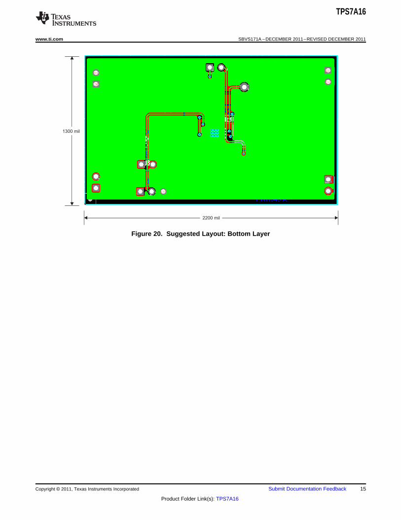
SUGGESTED LAYOUT AND SCHEMATIC
Layout is a critical part of good power-supply design. There are several signal paths that conduct fast-changingcurrents or voltages that can interact with stray inductance or parasitic capacitance to generate noise or degradethe power-supply performance. To help eliminate these problems, the IN pin should be bypassed to ground witha low ESR ceramic bypass capacitor with a X5R or X7R dielectric.
It may be possible to obtain acceptable performance with alternative PCB layouts; however, the layout and theschematic have been shown to produce good results and are meant as a guideline.
Figure 18 shows the schematic for the suggested layout.Figure 19 and Figure 20 show the top and bottomprinted circuit board (PCB) layers for the suggested layout.
Figure 18. Schematic for Suggested Layout
Figure 19. Suggested Layout: Top Layer
14 Submit Documentation Feedback Copyright © 2011, Texas Instruments Incorporated
Product Folder Link(s): TPS7A16
1300 mil
2200 mil
TPS7A16
www.ti.com SBVS171A –DECEMBER 2011–REVISED DECEMBER 2011
Figure 20. Suggested Layout: Bottom Layer
Copyright © 2011, Texas Instruments Incorporated Submit Documentation Feedback 15
Product Folder Link(s): TPS7A16

PACKAGE OPTION ADDENDUM
www.ti.com 16-Jan-2012
Addendum-Page 1
PACKAGING INFORMATION
Orderable Device Status (1) Package Type PackageDrawing
Pins Package Qty Eco Plan (2) Lead/Ball Finish
MSL Peak Temp (3) Samples
(Requires Login)
TPS7A1601DGNR ACTIVE MSOP-PowerPAD
DGN 8 2500 Green (RoHS& no Sb/Br)
CU NIPDAU Level-2-260C-1 YEAR
TPS7A1601DGNT ACTIVE MSOP-PowerPAD
DGN 8 250 Green (RoHS& no Sb/Br)
CU NIPDAU Level-2-260C-1 YEAR
TPS7A1633DGNR PREVIEW MSOP-PowerPAD
DGN 8 2500 Green (RoHS& no Sb/Br)
CU NIPDAU Level-2-260C-1 YEAR
TPS7A1633DGNT PREVIEW MSOP-PowerPAD
DGN 8 250 Green (RoHS& no Sb/Br)
CU NIPDAU Level-2-260C-1 YEAR
TPS7A1650DGNR PREVIEW MSOP-PowerPAD
DGN 8 2500 Green (RoHS& no Sb/Br)
CU NIPDAU Level-2-260C-1 YEAR
TPS7A1650DGNT PREVIEW MSOP-PowerPAD
DGN 8 250 Green (RoHS& no Sb/Br)
CU NIPDAU Level-2-260C-1 YEAR
(1) The marketing status values are defined as follows:ACTIVE: Product device recommended for new designs.LIFEBUY: TI has announced that the device will be discontinued, and a lifetime-buy period is in effect.NRND: Not recommended for new designs. Device is in production to support existing customers, but TI does not recommend using this part in a new design.PREVIEW: Device has been announced but is not in production. Samples may or may not be available.OBSOLETE: TI has discontinued the production of the device.
(2) Eco Plan - The planned eco-friendly classification: Pb-Free (RoHS), Pb-Free (RoHS Exempt), or Green (RoHS & no Sb/Br) - please check http://www.ti.com/productcontent for the latest availabilityinformation and additional product content details.TBD: The Pb-Free/Green conversion plan has not been defined.Pb-Free (RoHS): TI's terms "Lead-Free" or "Pb-Free" mean semiconductor products that are compatible with the current RoHS requirements for all 6 substances, including the requirement thatlead not exceed 0.1% by weight in homogeneous materials. Where designed to be soldered at high temperatures, TI Pb-Free products are suitable for use in specified lead-free processes.Pb-Free (RoHS Exempt): This component has a RoHS exemption for either 1) lead-based flip-chip solder bumps used between the die and package, or 2) lead-based die adhesive used betweenthe die and leadframe. The component is otherwise considered Pb-Free (RoHS compatible) as defined above.Green (RoHS & no Sb/Br): TI defines "Green" to mean Pb-Free (RoHS compatible), and free of Bromine (Br) and Antimony (Sb) based flame retardants (Br or Sb do not exceed 0.1% by weightin homogeneous material)
(3) MSL, Peak Temp. -- The Moisture Sensitivity Level rating according to the JEDEC industry standard classifications, and peak solder temperature.
Important Information and Disclaimer:The information provided on this page represents TI's knowledge and belief as of the date that it is provided. TI bases its knowledge and belief on informationprovided by third parties, and makes no representation or warranty as to the accuracy of such information. Efforts are underway to better integrate information from third parties. TI has taken andcontinues to take reasonable steps to provide representative and accurate information but may not have conducted destructive testing or chemical analysis on incoming materials and chemicals.TI and TI suppliers consider certain information to be proprietary, and thus CAS numbers and other limited information may not be available for release.

PACKAGE OPTION ADDENDUM
www.ti.com 16-Jan-2012
Addendum-Page 2
In no event shall TI's liability arising out of such information exceed the total purchase price of the TI part(s) at issue in this document sold by TI to Customer on an annual basis.


IMPORTANT NOTICE
Texas Instruments Incorporated and its subsidiaries (TI) reserve the right to make corrections, modifications, enhancements, improvements,and other changes to its products and services at any time and to discontinue any product or service without notice. Customers shouldobtain the latest relevant information before placing orders and should verify that such information is current and complete. All products aresold subject to TI’s terms and conditions of sale supplied at the time of order acknowledgment.
TI warrants performance of its hardware products to the specifications applicable at the time of sale in accordance with TI’s standardwarranty. Testing and other quality control techniques are used to the extent TI deems necessary to support this warranty. Except wheremandated by government requirements, testing of all parameters of each product is not necessarily performed.
TI assumes no liability for applications assistance or customer product design. Customers are responsible for their products andapplications using TI components. To minimize the risks associated with customer products and applications, customers should provideadequate design and operating safeguards.
TI does not warrant or represent that any license, either express or implied, is granted under any TI patent right, copyright, mask work right,or other TI intellectual property right relating to any combination, machine, or process in which TI products or services are used. Informationpublished by TI regarding third-party products or services does not constitute a license from TI to use such products or services or awarranty or endorsement thereof. Use of such information may require a license from a third party under the patents or other intellectualproperty of the third party, or a license from TI under the patents or other intellectual property of TI.
Reproduction of TI information in TI data books or data sheets is permissible only if reproduction is without alteration and is accompaniedby all associated warranties, conditions, limitations, and notices. Reproduction of this information with alteration is an unfair and deceptivebusiness practice. TI is not responsible or liable for such altered documentation. Information of third parties may be subject to additionalrestrictions.
Resale of TI products or services with statements different from or beyond the parameters stated by TI for that product or service voids allexpress and any implied warranties for the associated TI product or service and is an unfair and deceptive business practice. TI is notresponsible or liable for any such statements.
TI products are not authorized for use in safety-critical applications (such as life support) where a failure of the TI product would reasonablybe expected to cause severe personal injury or death, unless officers of the parties have executed an agreement specifically governingsuch use. Buyers represent that they have all necessary expertise in the safety and regulatory ramifications of their applications, andacknowledge and agree that they are solely responsible for all legal, regulatory and safety-related requirements concerning their productsand any use of TI products in such safety-critical applications, notwithstanding any applications-related information or support that may beprovided by TI. Further, Buyers must fully indemnify TI and its representatives against any damages arising out of the use of TI products insuch safety-critical applications.
TI products are neither designed nor intended for use in military/aerospace applications or environments unless the TI products arespecifically designated by TI as military-grade or "enhanced plastic." Only products designated by TI as military-grade meet militaryspecifications. Buyers acknowledge and agree that any such use of TI products which TI has not designated as military-grade is solely atthe Buyer's risk, and that they are solely responsible for compliance with all legal and regulatory requirements in connection with such use.
TI products are neither designed nor intended for use in automotive applications or environments unless the specific TI products aredesignated by TI as compliant with ISO/TS 16949 requirements. Buyers acknowledge and agree that, if they use any non-designatedproducts in automotive applications, TI will not be responsible for any failure to meet such requirements.
Following are URLs where you can obtain information on other Texas Instruments products and application solutions:
Products Applications
Audio www.ti.com/audio Automotive and Transportation www.ti.com/automotive
Amplifiers amplifier.ti.com Communications and Telecom www.ti.com/communications
Data Converters dataconverter.ti.com Computers and Peripherals www.ti.com/computers
DLP® Products www.dlp.com Consumer Electronics www.ti.com/consumer-apps
DSP dsp.ti.com Energy and Lighting www.ti.com/energy
Clocks and Timers www.ti.com/clocks Industrial www.ti.com/industrial
Interface interface.ti.com Medical www.ti.com/medical
Logic logic.ti.com Security www.ti.com/security
Power Mgmt power.ti.com Space, Avionics and Defense www.ti.com/space-avionics-defense
Microcontrollers microcontroller.ti.com Video and Imaging www.ti.com/video
RFID www.ti-rfid.com
OMAP Mobile Processors www.ti.com/omap
Wireless Connectivity www.ti.com/wirelessconnectivity
TI E2E Community Home Page e2e.ti.com
Mailing Address: Texas Instruments, Post Office Box 655303, Dallas, Texas 75265Copyright © 2012, Texas Instruments Incorporated


![Mobilizing Call Of Duty - The Khronos Group Inc...' v o s µ o l v K ] u ] Ì ] } v Z v W ² D ] v ] u ] Ì Á ] Z ] v P YN&PG%HJLQ5HQGHU3DVV FRPPDQG%XIIHU EHJLQ,QIR FRQWHQWV YN&PG(QG5HQGHU3DVV](https://static.fdocuments.us/doc/165x107/60a92f27682ad92c5e53f24d/mobilizing-call-of-duty-the-khronos-group-inc-v-o-s-o-l-v-k-u-oe.jpg)