DE0-CV Computer System -...
41
DE0-CV Computer System For Quartus II 15.0 1 Introduction This document describes a computer system that can be implemented on the Altera DE0-CV development and educa- tion board. This system, called the DE0-CV Computer, is intended for use in experiments on computer organization and embedded systems. To support such experiments, the system contains embedded processors, memory, video ports, and some simple I/O peripherals. The FPGA programming file that implements this system, as well as its design source files, can be obtained from the University Program section of Altera’s web site. 2 DE0-CV Computer Contents A block diagram of the DE0-CV Computer system is shown in Figure 1. As indicated in the figure, the components in this system are implemented in the Altera Cyclone R V FPGA chip. The FPGA implements two Nios II processors and several peripheral ports: memory, timer modules, video-in/out, PS/2, and parallel ports connected to switches and lights. 2.1 FPGA Components As shown in Figure 1 many of the components in the DE0-CV Computer are implemented inside the FPGA in the Cyclone V SoC chip. Several of these components are described in this section, and the others are presented in Section 4. 2.2 Nios II Processor The Altera Nios R II processor is a 32-bit CPU that can be implemented in an Altera FPGA device. Three versions of the Nios II processor are available, designated economy (/e), standard (/s), and fast (/f). The DE0-CV Computer includes two Nios II processors, both of which are the fast version. An overview of the Nios II processor can be found in the document Introduction to the Altera Nios II Processor, which is provided in the University Program’s web site. An easy way to begin working with the DE0-CV Computer and the Nios II processor is to make use of a utility called the Altera Monitor Program. It provides an easy way to assemble/compile Nios II programs written in either assembly language or the C language. The Monitor Program, which can be downloaded from Altera’s web site, is an application program that runs on the host computer connected to the DE0-CV board. The Monitor Program can be used to control the execution of code on Nios II, list (and edit) the contents of processor registers, display/edit the contents of memory on the DE0-CV board, and similar operations. The Monitor Program includes the DE0-CV Computer as a predesigned system that can be downloaded onto the DE0-CV board, as well as several sample programs in assembly language and C that show how to use Altera Corporation - University Program 2015 1
Transcript of DE0-CV Computer System -...

DE0-CV Computer System
For Quartus II 15.0
1 Introduction
This document describes a computer system that can be implemented on the Altera DE0-CV development and educa-tion board. This system, called the DE0-CV Computer, is intended for use in experiments on computer organizationand embedded systems. To support such experiments, the system contains embedded processors, memory, videoports, and some simple I/O peripherals. The FPGA programming file that implements this system, as well as itsdesign source files, can be obtained from the University Program section of Altera’s web site.
2 DE0-CV Computer Contents
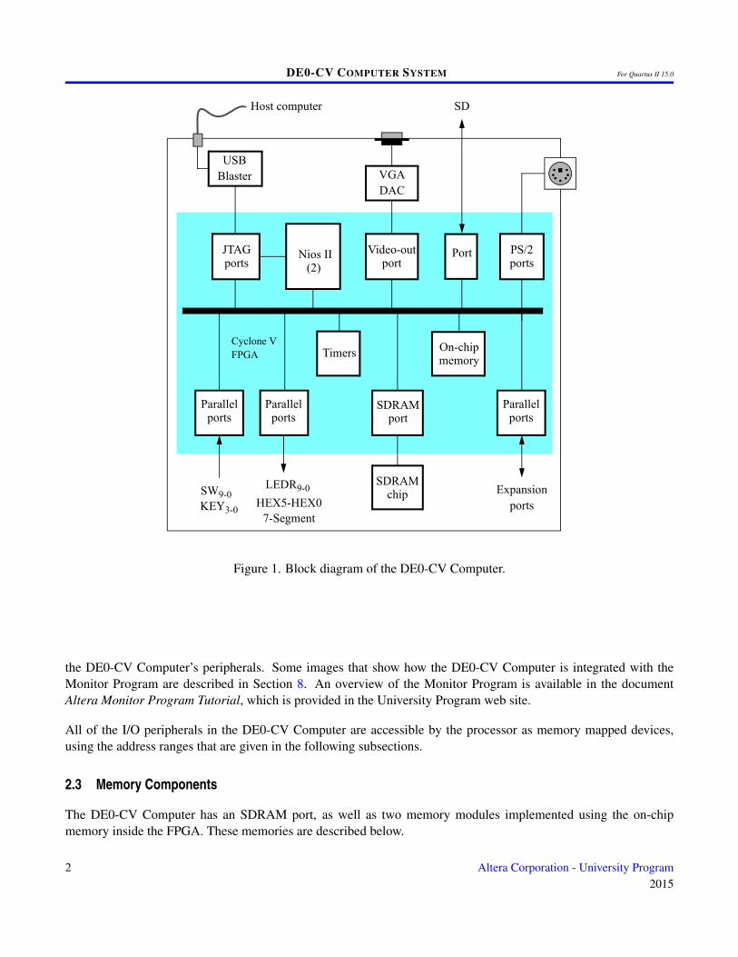
A block diagram of the DE0-CV Computer system is shown in Figure 1. As indicated in the figure, the componentsin this system are implemented in the Altera Cyclone R©V FPGA chip. The FPGA implements two Nios II processorsand several peripheral ports: memory, timer modules, video-in/out, PS/2, and parallel ports connected to switchesand lights.
2.1 FPGA Components
As shown in Figure 1 many of the components in the DE0-CV Computer are implemented inside the FPGA in theCyclone V SoC chip. Several of these components are described in this section, and the others are presented inSection 4.
2.2 Nios II Processor
The Altera Nios R©II processor is a 32-bit CPU that can be implemented in an Altera FPGA device. Three versionsof the Nios II processor are available, designated economy (/e), standard (/s), and fast (/f). The DE0-CV Computerincludes two Nios II processors, both of which are the fast version.
An overview of the Nios II processor can be found in the document Introduction to the Altera Nios II Processor,which is provided in the University Program’s web site. An easy way to begin working with the DE0-CV Computerand the Nios II processor is to make use of a utility called the Altera Monitor Program. It provides an easy way toassemble/compile Nios II programs written in either assembly language or the C language. The Monitor Program,which can be downloaded from Altera’s web site, is an application program that runs on the host computer connectedto the DE0-CV board. The Monitor Program can be used to control the execution of code on Nios II, list (andedit) the contents of processor registers, display/edit the contents of memory on the DE0-CV board, and similaroperations. The Monitor Program includes the DE0-CV Computer as a predesigned system that can be downloadedonto the DE0-CV board, as well as several sample programs in assembly language and C that show how to use
Altera Corporation - University Program2015
1
DE0-CV COMPUTER SYSTEM For Quartus II 15.0
Expansionports
Cyclone VFPGA
PS/2ports
Timers
SW9-0LEDR9-0
Parallelports
Parallelports
HEX5-HEX07-Segment
KEY3-0
SDRAMport
SDRAMchip
SD
On-chipmemory
Host computer
USBBlaster VGA
DAC
Video-outport
PortJTAGports
Parallelports
Nios II(2)
Figure 1. Block diagram of the DE0-CV Computer.
the DE0-CV Computer’s peripherals. Some images that show how the DE0-CV Computer is integrated with theMonitor Program are described in Section 8. An overview of the Monitor Program is available in the documentAltera Monitor Program Tutorial, which is provided in the University Program web site.
All of the I/O peripherals in the DE0-CV Computer are accessible by the processor as memory mapped devices,using the address ranges that are given in the following subsections.
2.3 Memory Components
The DE0-CV Computer has an SDRAM port, as well as two memory modules implemented using the on-chipmemory inside the FPGA. These memories are described below.
2 Altera Corporation - University Program2015
DE0-CV COMPUTER SYSTEM For Quartus II 15.0
2.3.1 SDRAM
An SDRAM Controller in the FPGA provides an interface to the 64 MB synchronous dynamic RAM (SDRAM)on the DE0-CV board, which is organized as 32M x 16 bits. It is accessible by the Nios II processor using word(32-bit), halfword (16-bit), or byte operations, and is mapped to the address space 0x00000000 to 0x03FFFFFF.
2.3.2 On-Chip Memory
The DE0-CV Computer includes a 256-Kbyte memory that is implemented inside the FPGA. This memory is orga-nized as 8K x 32 bits, and spans addresses in the range 0x08000000 to 0x0803FFFF. The memory is used as apixel buffer for the video-out port.
2.3.3 On-Chip Memory Character Buffer
The DE0-CV Computer includes an 8-Kbyte memory implemented inside the FPGA that is used as a character bufferfor the video-out port, which is described in Section 4.1. The character buffer memory is organized as 8K x 8 bits,and spans the address range 0x09000000 to 0x09001FFF.
2.4 Parallel Ports
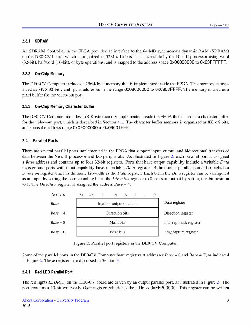
There are several parallel ports implemented in the FPGA that support input, output, and bidirectional transfers ofdata between the Nios II processor and I/O peripherals. As illustrated in Figure 2, each parallel port is assigneda Base address and contains up to four 32-bit registers. Ports that have output capability include a writable Dataregister, and ports with input capability have a readable Data register. Bidirectional parallel ports also include aDirection register that has the same bit-width as the Data register. Each bit in the Data register can be configuredas an input by setting the corresponding bit in the Direction register to 0, or as an output by setting this bit positionto 1. The Direction register is assigned the address Base + 4.
Address 02 14 331 30 . . .
Base
Base + 8
Base + C
Base + 4
Input or output data bits
Direction bits
Edge bits
Mask bits
Data register
Direction register
Interruptmask register
Edgecapture register
Direction bits
Figure 2. Parallel port registers in the DE0-CV Computer.
Some of the parallel ports in the DE0-CV Computer have registers at addresses Base + 8 and Base + C, as indicatedin Figure 2. These registers are discussed in Section 3.
2.4.1 Red LED Parallel Port
The red lights LEDR9−0 on the DE0-CV board are driven by an output parallel port, as illustrated in Figure 3. Theport contains a 10-bit write-only Data register, which has the address 0xFF200000. This register can be written
Altera Corporation - University Program2015
3
DE0-CV COMPUTER SYSTEM For Quartus II 15.0
using word accesses, and the upper bits not used in the registers are ignored.
0xFF200000
LEDR0LEDR9
Address
031 910 . . .Unused Data register
Figure 3. Output parallel port for LEDR.
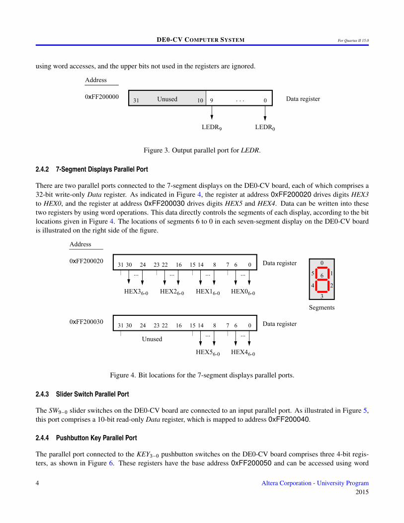
2.4.2 7-Segment Displays Parallel Port
There are two parallel ports connected to the 7-segment displays on the DE0-CV board, each of which comprises a32-bit write-only Data register. As indicated in Figure 4, the register at address 0xFF200020 drives digits HEX3to HEX0, and the register at address 0xFF200030 drives digits HEX5 and HEX4. Data can be written into thesetwo registers by using word operations. This data directly controls the segments of each display, according to the bitlocations given in Figure 4. The locations of segments 6 to 0 in each seven-segment display on the DE0-CV boardis illustrated on the right side of the figure.
0xFF200020
...
HEX06-0
...
HEX16-0
...
HEX36-0
Address
07 6815 142431 30
0xFF200030
...
HEX26-0
1623 22
...
HEX46-0
...
HEX56-0
07 6815 142431 30 1623 22
Data register
Data register
0
1
2
3
4
5 6
Segments
Unused
Figure 4. Bit locations for the 7-segment displays parallel ports.
2.4.3 Slider Switch Parallel Port
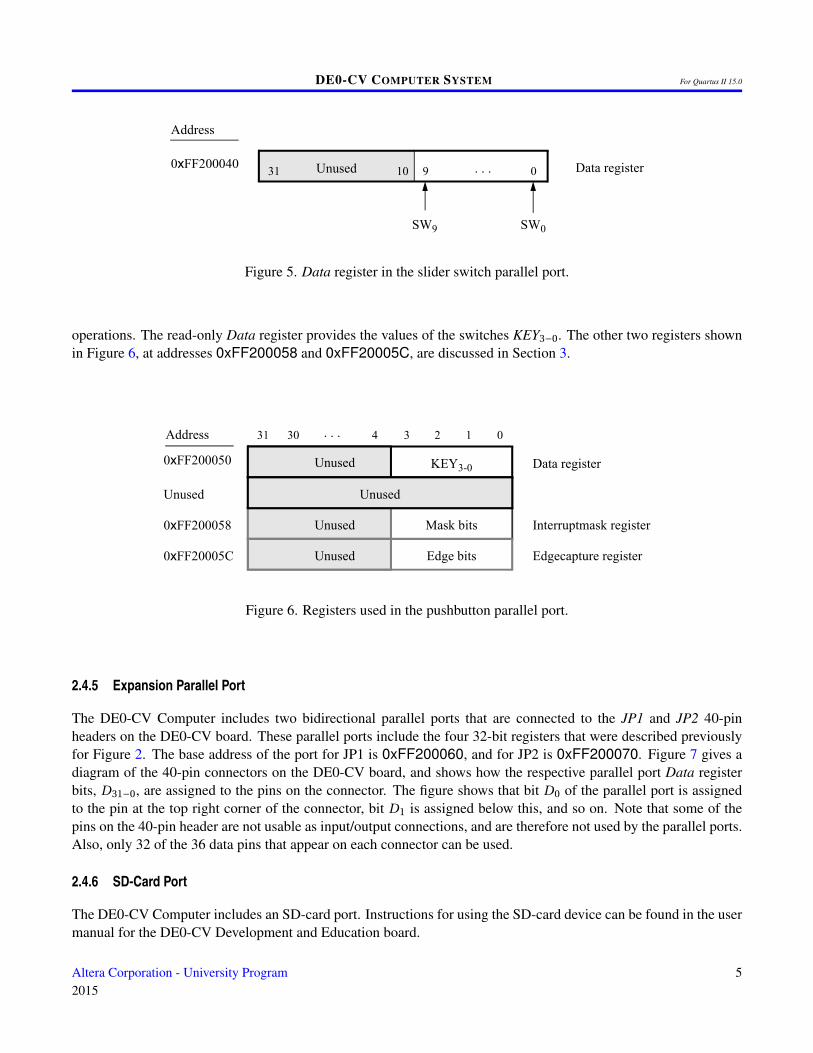
The SW9−0 slider switches on the DE0-CV board are connected to an input parallel port. As illustrated in Figure 5,this port comprises a 10-bit read-only Data register, which is mapped to address 0xFF200040.
2.4.4 Pushbutton Key Parallel Port
The parallel port connected to the KEY3−0 pushbutton switches on the DE0-CV board comprises three 4-bit regis-ters, as shown in Figure 6. These registers have the base address 0xFF200050 and can be accessed using word
4 Altera Corporation - University Program2015
DE0-CV COMPUTER SYSTEM For Quartus II 15.0
0xFF200040
SW0SW9
Address
Data register031 910 . . .Unused
Figure 5. Data register in the slider switch parallel port.
operations. The read-only Data register provides the values of the switches KEY3−0. The other two registers shownin Figure 6, at addresses 0xFF200058 and 0xFF20005C, are discussed in Section 3.
Address 02 14 331 30 . . .
0xFF200050
0xFF200058
0xFF20005C
Unused
KEY3-0
Edge bits
Mask bits
Unused
Unused
Unused
Data register
Interruptmask register
Edgecapture register
Unused
Figure 6. Registers used in the pushbutton parallel port.
2.4.5 Expansion Parallel Port
The DE0-CV Computer includes two bidirectional parallel ports that are connected to the JP1 and JP2 40-pinheaders on the DE0-CV board. These parallel ports include the four 32-bit registers that were described previouslyfor Figure 2. The base address of the port for JP1 is 0xFF200060, and for JP2 is 0xFF200070. Figure 7 gives adiagram of the 40-pin connectors on the DE0-CV board, and shows how the respective parallel port Data registerbits, D31−0, are assigned to the pins on the connector. The figure shows that bit D0 of the parallel port is assignedto the pin at the top right corner of the connector, bit D1 is assigned below this, and so on. Note that some of thepins on the 40-pin header are not usable as input/output connections, and are therefore not used by the parallel ports.Also, only 32 of the 36 data pins that appear on each connector can be used.
2.4.6 SD-Card Port
The DE0-CV Computer includes an SD-card port. Instructions for using the SD-card device can be found in the usermanual for the DE0-CV Development and Education board.
Altera Corporation - University Program2015
5

DE0-CV COMPUTER SYSTEM For Quartus II 15.0
D0D1
D2 D3D4 D5D6 D7Unused
D10 D11D12 D13
D14D15
D16 D17D18 D19
D22 D23D24 D25D26 D27D28 D29D30 D31
Unused
JP1 JP2
Pin 1 Pin 1
Pin 40 Pin 40
D8 D9
D20 D21
D0D1
D2 D3D4 D5D6 D7Unused
D10 D11D12 D13
D14D15
D16 D17D18 D19
D22 D23D24 D25D26 D27D28 D29D30 D31
Unused
D8 D9
D20 D21
Figure 7. Assignment of parallel port bits to pins on JP1 and JP2.
2.4.7 Using the Parallel Ports with Assembly Language Code and C Code
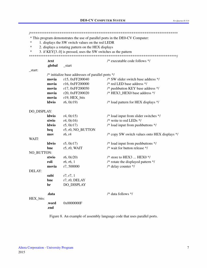
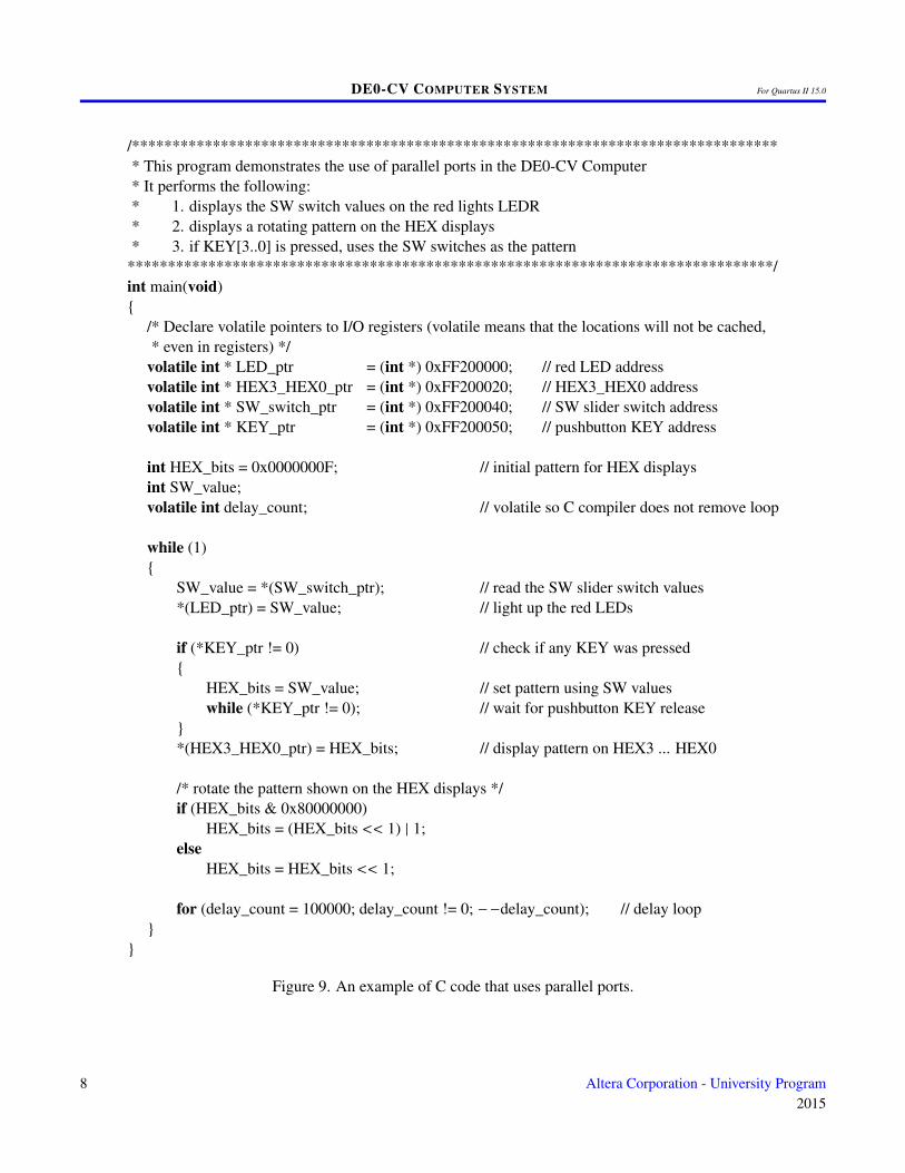
The DE0-CV Computer provides a convenient platform for experimenting with Nios II assembly language code, orC code. A simple example of such code is provided in Figures 8 and 9. Both programs perform the same operations,and illustrate the use of parallel ports by using either assembly language or C code.
The code in the figures displays the values of the SW switches on the red lights LEDR. It also displays a rotatingpattern on 7-segment displays HEX3, . . ., HEX0. This pattern is rotated to the left by using a Nios II rotate instruction,and a delay loop is used to make the shifting slow enough to observe. The pattern on the HEX displays can bechanged to the values of the SW switches by pressing any of pushbuttons KEY3−0. When a pushbutton key ispressed, the program waits in a loop until the key is released.
The source code files shown in Figures 8 and 9 are distributed as part of the Altera Monitor Program. The files canbe found under the heading sample programs, and are identified by the name Getting Started.
6 Altera Corporation - University Program2015
DE0-CV COMPUTER SYSTEM For Quartus II 15.0
/********************************************************************************* This program demonstrates the use of parallel ports in the DE0-CV Computer:* 1. displays the SW switch values on the red LEDR* 2. displays a rotating pattern on the HEX displays* 3. if KEY[3..0] is pressed, uses the SW switches as the pattern
********************************************************************************/.text /* executable code follows */.global _start
_start:/* initialize base addresses of parallel ports */movia r15, 0xFF200040 /* SW slider switch base address */movia r16, 0xFF200000 /* red LED base address */movia r17, 0xFF200050 /* pushbutton KEY base address */movia r20, 0xFF200020 /* HEX3_HEX0 base address */movia r19, HEX_bitsldwio r6, 0(r19) /* load pattern for HEX displays */
DO_DISPLAY:ldwio r4, 0(r15) /* load input from slider switches */stwio r4, 0(r16) /* write to red LEDs */ldwio r5, 0(r17) /* load input from pushbuttons */beq r5, r0, NO_BUTTONmov r6, r4 /* copy SW switch values onto HEX displays */
WAIT:ldwio r5, 0(r17) /* load input from pushbuttons */bne r5, r0, WAIT /* wait for button release */
NO_BUTTON:stwio r6, 0(r20) /* store to HEX3 ... HEX0 */roli r6, r6, 1 /* rotate the displayed pattern */movia r7, 500000 /* delay counter */
DELAY:subi r7, r7, 1bne r7, r0, DELAYbr DO_DISPLAY
.data /* data follows */HEX_bits:
.word 0x0000000F
.end
Figure 8. An example of assembly language code that uses parallel ports.
Altera Corporation - University Program2015
7
DE0-CV COMPUTER SYSTEM For Quartus II 15.0
/********************************************************************************* This program demonstrates the use of parallel ports in the DE0-CV Computer* It performs the following:* 1. displays the SW switch values on the red lights LEDR* 2. displays a rotating pattern on the HEX displays* 3. if KEY[3..0] is pressed, uses the SW switches as the pattern
********************************************************************************/int main(void){
/* Declare volatile pointers to I/O registers (volatile means that the locations will not be cached,* even in registers) */
volatile int * LED_ptr = (int *) 0xFF200000; // red LED addressvolatile int * HEX3_HEX0_ptr = (int *) 0xFF200020; // HEX3_HEX0 addressvolatile int * SW_switch_ptr = (int *) 0xFF200040; // SW slider switch addressvolatile int * KEY_ptr = (int *) 0xFF200050; // pushbutton KEY address
int HEX_bits = 0x0000000F; // initial pattern for HEX displaysint SW_value;volatile int delay_count; // volatile so C compiler does not remove loop
while (1){
SW_value = *(SW_switch_ptr); // read the SW slider switch values*(LED_ptr) = SW_value; // light up the red LEDs
if (*KEY_ptr != 0) // check if any KEY was pressed{
HEX_bits = SW_value; // set pattern using SW valueswhile (*KEY_ptr != 0); // wait for pushbutton KEY release
}*(HEX3_HEX0_ptr) = HEX_bits; // display pattern on HEX3 ... HEX0
/* rotate the pattern shown on the HEX displays */if (HEX_bits & 0x80000000)
HEX_bits = (HEX_bits << 1) | 1;else
HEX_bits = HEX_bits << 1;
for (delay_count = 100000; delay_count != 0; −−delay_count); // delay loop}
}
Figure 9. An example of C code that uses parallel ports.
8 Altera Corporation - University Program2015
DE0-CV COMPUTER SYSTEM For Quartus II 15.0
2.5 JTAG Port
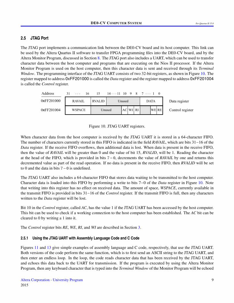
The JTAG port implements a communication link between the DE0-CV board and its host computer. This link canbe used by the Altera Quartus II software to transfer FPGA programming files into the DE0-CV board, and by theAltera Monitor Program, discussed in Section 8. The JTAG port also includes a UART, which can be used to transfercharacter data between the host computer and programs that are executing on the Nios II processor. If the AlteraMonitor Program is used on the host computer, then this character data is sent and received through its TerminalWindow. The programming interface of the JTAG UART consists of two 32-bit registers, as shown in Figure 10. Theregister mapped to address 0xFF201000 is called the Data register and the register mapped to address 0xFF201004is called the Control register.
Address 0731 16. . .
0xFF201000
0xFF201004
DATARAVAIL
14 8. . . . . .
WSPACE Unused WI RI WE RE
1
RVALID
AC
10 911
Unused
15
Data register
Control register
Figure 10. JTAG UART registers.
When character data from the host computer is received by the JTAG UART it is stored in a 64-character FIFO.The number of characters currently stored in this FIFO is indicated in the field RAVAIL, which are bits 31−16 of theData register. If the receive FIFO overflows, then additional data is lost. When data is present in the receive FIFO,then the value of RAVAIL will be greater than 0 and the value of bit 15, RVALID, will be 1. Reading the characterat the head of the FIFO, which is provided in bits 7−0, decrements the value of RAVAIL by one and returns thisdecremented value as part of the read operation. If no data is present in the receive FIFO, then RVALID will be setto 0 and the data in bits 7−0 is undefined.
The JTAG UART also includes a 64-character FIFO that stores data waiting to be transmitted to the host computer.Character data is loaded into this FIFO by performing a write to bits 7−0 of the Data register in Figure 10. Notethat writing into this register has no effect on received data. The amount of space, WSPACE, currently available inthe transmit FIFO is provided in bits 31−16 of the Control register. If the transmit FIFO is full, then any characterswritten to the Data register will be lost.
Bit 10 in the Control register, called AC, has the value 1 if the JTAG UART has been accessed by the host computer.This bit can be used to check if a working connection to the host computer has been established. The AC bit can becleared to 0 by writing a 1 into it.
The Control register bits RE, WE, RI, and WI are described in Section 3.
2.5.1 Using the JTAG UART with Assembly Language Code and C Code
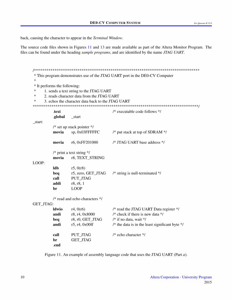
Figures 11 and 13 give simple examples of assembly language and C code, respectively, that use the JTAG UART.Both versions of the code perform the same function, which is to first send an ASCII string to the JTAG UART, andthen enter an endless loop. In the loop, the code reads character data that has been received by the JTAG UART,and echoes this data back to the UART for transmission. If the program is executed by using the Altera MonitorProgram, then any keyboard character that is typed into the Terminal Window of the Monitor Program will be echoed
Altera Corporation - University Program2015
9
DE0-CV COMPUTER SYSTEM For Quartus II 15.0
back, causing the character to appear in the Terminal Window.
The source code files shown in Figures 11 and 13 are made available as part of the Altera Monitor Program. Thefiles can be found under the heading sample programs, and are identified by the name JTAG UART.
/********************************************************************************* This program demonstrates use of the JTAG UART port in the DE0-CV Computer** It performs the following:* 1. sends a text string to the JTAG UART* 2. reads character data from the JTAG UART* 3. echos the character data back to the JTAG UART
********************************************************************************/.text /* executable code follows */.global _start
_start:/* set up stack pointer */movia sp, 0x03FFFFFC /* put stack at top of SDRAM */
movia r6, 0xFF201000 /* JTAG UART base address */
/* print a text string */movia r8, TEXT_STRING
LOOP:ldb r5, 0(r8)beq r5, zero, GET_JTAG /* string is null-terminated */call PUT_JTAGaddi r8, r8, 1br LOOP
/* read and echo characters */GET_JTAG:
ldwio r4, 0(r6) /* read the JTAG UART Data register */andi r8, r4, 0x8000 /* check if there is new data */beq r8, r0, GET_JTAG /* if no data, wait */andi r5, r4, 0x00ff /* the data is in the least significant byte */
call PUT_JTAG /* echo character */br GET_JTAG.end
Figure 11. An example of assembly language code that uses the JTAG UART (Part a).
10 Altera Corporation - University Program2015
DE0-CV COMPUTER SYSTEM For Quartus II 15.0
/********************************************************************************* Subroutine to send a character to the JTAG UART* r5 = character to send* r6 = JTAG UART base address
********************************************************************************/.global PUT_JTAG
PUT_JTAG:/* save any modified registers */subi sp, sp, 4 /* reserve space on the stack */stw r4, 0(sp) /* save register */
ldwio r4, 4(r6) /* read the JTAG UART Control register */andhi r4, r4, 0xffff /* check for write space */beq r4, r0, END_PUT /* if no space, ignore the character */stwio r5, 0(r6) /* send the character */
END_PUT:/* restore registers */ldw r4, 0(sp)addi sp, sp, 4
ret
.data /* data follows */TEXT_STRING:
.asciz "\nJTAG UART example code\n> "
.end
Figure 11. An example of assembly language code that uses the JTAG UART (Part b).
Altera Corporation - University Program2015
11
DE0-CV COMPUTER SYSTEM For Quartus II 15.0
/* function prototypes */void put_jtag(char);char get_jtag(void);/********************************************************************************* This program demonstrates use of the JTAG UART port in the DE0-CV Computer* It performs the following:* 1. sends a text string to the JTAG UART* 2. reads and echos character data from/to the JTAG UART
********************************************************************************/int main(void){
char text_string[] = "\nJTAG UART example code\n> \0";char *str, c;
/* print a text string */for (str = text_string; *str != 0; ++str)
put_jtag (*str);/* read and echo characters */while (1){
c = get_jtag ( );if (c != ’\0’)
put_jtag (c);}
}
/********************************************************************************* Subroutine to send a character to the JTAG UART
********************************************************************************/void put_jtag( char c ){
volatile int * JTAG_UART_ptr = (int *) 0xFF201000; // JTAG UART addressint control;control = *(JTAG_UART_ptr + 1); // read the JTAG_UART control registerif (control & 0xFFFF0000) // if space, echo character, else ignore
*(JTAG_UART_ptr) = c;}
Figure 12. An example of C code that uses the JTAG UART (Part a).
12 Altera Corporation - University Program2015
DE0-CV COMPUTER SYSTEM For Quartus II 15.0
/********************************************************************************* Subroutine to read a character from the JTAG UART* Returns \0 if no character, otherwise returns the character
********************************************************************************/char get_jtag( void ){
volatile int * JTAG_UART_ptr = (int *) 0xFF201000; // JTAG UART addressint data;data = *(JTAG_UART_ptr); // read the JTAG_UART data registerif (data & 0x00008000) // check RVALID to see if there is new data
return ((char) data & 0xFF);else
return (’\0’);}
Figure 13. An example of C code that uses the JTAG UART (Part b).
2.6 Interval Timers
The DE0-CV Computer includes a timer module implemented in the FPGA that can be used by the Nios II pro-cessor. This timer can be loaded with a preset value, and then counts down to zero using a 100-MHz clock. Theprogramming interface for the timer includes six 16-bit registers, as illustrated in Figure 14. The 16-bit register ataddress 0xFF202000 provides status information about the timer, and the register at address 0xFF202004 allowscontrol settings to be made. The bit fields in these registers are described below:
• TO provides a timeout signal which is set to 1 by the timer when it has reached a count value of zero. The TObit can be reset by writing a 0 into it.
• RUN is set to 1 by the timer whenever it is currently counting.
• ITO is used for generating interrupts, which are discussed in section 3.
• CONT affects the continuous operation of the timer. When the timer reaches a count value of zero it auto-matically reloads the specified starting count value. If CONT is set to 1, then the timer will continue countingdown automatically. But if CONT = 0, then the timer will stop after it has reached a count value of 0.
• (START/STOP) is used to commence/suspend the operation of the timer by writing a 1 into the respective bit.
The two 16-bit registers at addresses 0xFF202008 and 0xFF20200C allow the period of the timer to be changedby setting the starting count value. The default setting provided in the DE0-CV Computer gives a timer periodof 125 msec. To achieve this period, the starting value of the count is 100 MHz × 125 msec = 12.5× 10⁶. It ispossible to capture a snapshot of the counter value at any time by performing a write to address 0xFF202010. Thiswrite operation causes the current 32-bit counter value to be stored into the two 16-bit timer registers at addresses0xFF202010 and 0xFF202014. These registers can then be read to obtain the count value.
A second interval timer, which has an identical interface to the one described above, is also available in the FPGA,starting at the base address 0xFF202020.
Altera Corporation - University Program2015
13
DE0-CV COMPUTER SYSTEM For Quartus II 15.0
Address 01531 . . .
0xFF202000
0xFF202004
. . .
Unused RUN TO
1
START CONT ITOSTOP
16 217
Unused
Counter start value (low) 0xFF202008
Counter start value (high)0xFF20200C
Counter snapshot (low)0xFF202010
Counter snapshot (high)0xFF202014
3
Not present(interval timer has16-bit registers)
Status register
Control register
Figure 14. Interval timer registers.
3 Exceptions and Interrupts
The reset address of the Nios II processor in the DE0-CV Computer is set to 0x00000000. The address usedfor all other general exceptions, such as divide by zero, and hardware IRQ interrupts is 0x00000020. Since theNios II processor uses the same address for general exceptions and hardware IRQ interrupts, the Exception Handlersoftware must determine the source of the exception by examining the appropriate processor status register. Table1 gives the assignment of IRQ numbers to each of the I/O peripherals in the DE0-CV Computer. The rest of thissection describes the interrupt behavior associated with the interval timer, parallel ports, and serial ports in theDE0-CV Computer. Interrupts for other devices listed in Table 1 are discussed in section 4.
I/O Peripheral IRQ #Interval timer 0Pushbutton switch parallel port 1Second Interval timer 2PS/2 port 7JTAG port 8Serial port 10JP1 Expansion parallel port 11JP2 Expansion parallel port 12
Table 1. Hardware IRQ interrupt assignment for the DE0-CV Computer.
14 Altera Corporation - University Program2015
DE0-CV COMPUTER SYSTEM For Quartus II 15.0
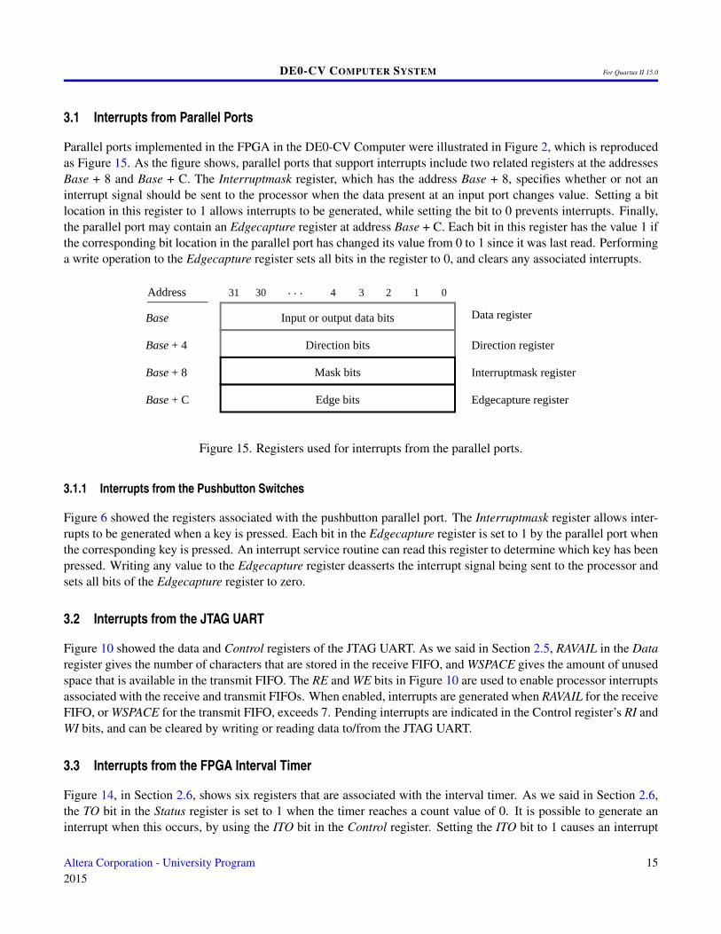
3.1 Interrupts from Parallel Ports
Parallel ports implemented in the FPGA in the DE0-CV Computer were illustrated in Figure 2, which is reproducedas Figure 15. As the figure shows, parallel ports that support interrupts include two related registers at the addressesBase + 8 and Base + C. The Interruptmask register, which has the address Base + 8, specifies whether or not aninterrupt signal should be sent to the processor when the data present at an input port changes value. Setting a bitlocation in this register to 1 allows interrupts to be generated, while setting the bit to 0 prevents interrupts. Finally,the parallel port may contain an Edgecapture register at address Base + C. Each bit in this register has the value 1 ifthe corresponding bit location in the parallel port has changed its value from 0 to 1 since it was last read. Performinga write operation to the Edgecapture register sets all bits in the register to 0, and clears any associated interrupts.
Address 02 14 331 30 . . .
Base
Base + 8
Base + C
Base + 4
Input or output data bits
Direction bits
Data register
Direction register
Interruptmask register
Edgecapture register Edge bits
Mask bits
Direction bits
Figure 15. Registers used for interrupts from the parallel ports.
3.1.1 Interrupts from the Pushbutton Switches
Figure 6 showed the registers associated with the pushbutton parallel port. The Interruptmask register allows inter-rupts to be generated when a key is pressed. Each bit in the Edgecapture register is set to 1 by the parallel port whenthe corresponding key is pressed. An interrupt service routine can read this register to determine which key has beenpressed. Writing any value to the Edgecapture register deasserts the interrupt signal being sent to the processor andsets all bits of the Edgecapture register to zero.
3.2 Interrupts from the JTAG UART
Figure 10 showed the data and Control registers of the JTAG UART. As we said in Section 2.5, RAVAIL in the Dataregister gives the number of characters that are stored in the receive FIFO, and WSPACE gives the amount of unusedspace that is available in the transmit FIFO. The RE and WE bits in Figure 10 are used to enable processor interruptsassociated with the receive and transmit FIFOs. When enabled, interrupts are generated when RAVAIL for the receiveFIFO, or WSPACE for the transmit FIFO, exceeds 7. Pending interrupts are indicated in the Control register’s RI andWI bits, and can be cleared by writing or reading data to/from the JTAG UART.
3.3 Interrupts from the FPGA Interval Timer
Figure 14, in Section 2.6, shows six registers that are associated with the interval timer. As we said in Section 2.6,the TO bit in the Status register is set to 1 when the timer reaches a count value of 0. It is possible to generate aninterrupt when this occurs, by using the ITO bit in the Control register. Setting the ITO bit to 1 causes an interrupt
Altera Corporation - University Program2015
15
DE0-CV COMPUTER SYSTEM For Quartus II 15.0
request to be sent to the processor whenever TO becomes 1. After an interrupt occurs, it can be cleared by writingany value into the Status register.
3.4 Using Interrupts with Assembly Language Code
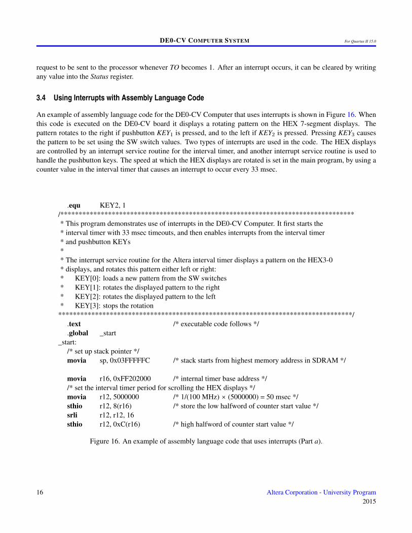
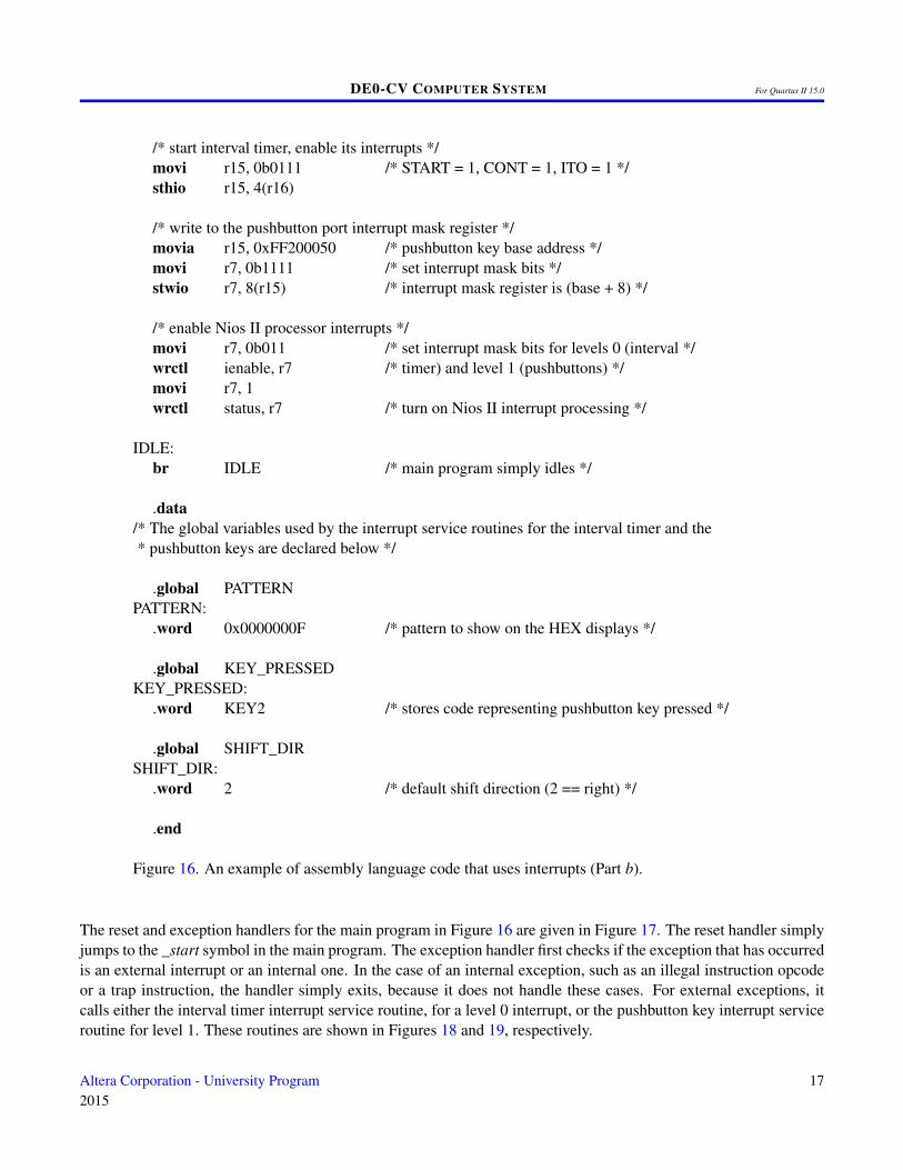
An example of assembly language code for the DE0-CV Computer that uses interrupts is shown in Figure 16. Whenthis code is executed on the DE0-CV board it displays a rotating pattern on the HEX 7-segment displays. Thepattern rotates to the right if pushbutton KEY1 is pressed, and to the left if KEY2 is pressed. Pressing KEY3 causesthe pattern to be set using the SW switch values. Two types of interrupts are used in the code. The HEX displaysare controlled by an interrupt service routine for the interval timer, and another interrupt service routine is used tohandle the pushbutton keys. The speed at which the HEX displays are rotated is set in the main program, by using acounter value in the interval timer that causes an interrupt to occur every 33 msec.
.equ KEY2, 1/********************************************************************************* This program demonstrates use of interrupts in the DE0-CV Computer. It first starts the* interval timer with 33 msec timeouts, and then enables interrupts from the interval timer* and pushbutton KEYs** The interrupt service routine for the Altera interval timer displays a pattern on the HEX3-0* displays, and rotates this pattern either left or right:* KEY[0]: loads a new pattern from the SW switches* KEY[1]: rotates the displayed pattern to the right* KEY[2]: rotates the displayed pattern to the left* KEY[3]: stops the rotation
********************************************************************************/.text /* executable code follows */.global _start
_start:/* set up stack pointer */movia sp, 0x03FFFFFC /* stack starts from highest memory address in SDRAM */
movia r16, 0xFF202000 /* internal timer base address *//* set the interval timer period for scrolling the HEX displays */movia r12, 5000000 /* 1/(100 MHz) × (5000000) = 50 msec */sthio r12, 8(r16) /* store the low halfword of counter start value */srli r12, r12, 16sthio r12, 0xC(r16) /* high halfword of counter start value */
Figure 16. An example of assembly language code that uses interrupts (Part a).
16 Altera Corporation - University Program2015
DE0-CV COMPUTER SYSTEM For Quartus II 15.0
/* start interval timer, enable its interrupts */movi r15, 0b0111 /* START = 1, CONT = 1, ITO = 1 */sthio r15, 4(r16)
/* write to the pushbutton port interrupt mask register */movia r15, 0xFF200050 /* pushbutton key base address */movi r7, 0b1111 /* set interrupt mask bits */stwio r7, 8(r15) /* interrupt mask register is (base + 8) */
/* enable Nios II processor interrupts */movi r7, 0b011 /* set interrupt mask bits for levels 0 (interval */wrctl ienable, r7 /* timer) and level 1 (pushbuttons) */movi r7, 1wrctl status, r7 /* turn on Nios II interrupt processing */
IDLE:br IDLE /* main program simply idles */
.data/* The global variables used by the interrupt service routines for the interval timer and the* pushbutton keys are declared below */
.global PATTERNPATTERN:
.word 0x0000000F /* pattern to show on the HEX displays */
.global KEY_PRESSEDKEY_PRESSED:
.word KEY2 /* stores code representing pushbutton key pressed */
.global SHIFT_DIRSHIFT_DIR:
.word 2 /* default shift direction (2 == right) */
.end
Figure 16. An example of assembly language code that uses interrupts (Part b).
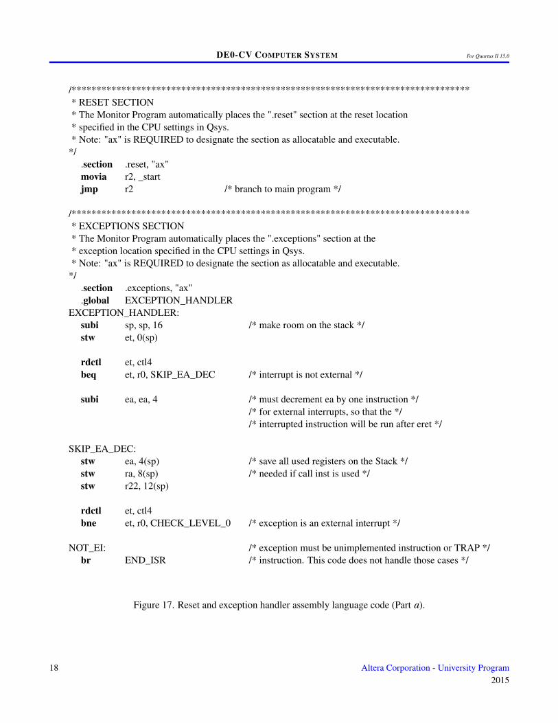
The reset and exception handlers for the main program in Figure 16 are given in Figure 17. The reset handler simplyjumps to the _start symbol in the main program. The exception handler first checks if the exception that has occurredis an external interrupt or an internal one. In the case of an internal exception, such as an illegal instruction opcodeor a trap instruction, the handler simply exits, because it does not handle these cases. For external exceptions, itcalls either the interval timer interrupt service routine, for a level 0 interrupt, or the pushbutton key interrupt serviceroutine for level 1. These routines are shown in Figures 18 and 19, respectively.
Altera Corporation - University Program2015
17
DE0-CV COMPUTER SYSTEM For Quartus II 15.0
/********************************************************************************* RESET SECTION* The Monitor Program automatically places the ".reset" section at the reset location* specified in the CPU settings in Qsys.* Note: "ax" is REQUIRED to designate the section as allocatable and executable.
*/.section .reset, "ax"movia r2, _startjmp r2 /* branch to main program */
/********************************************************************************* EXCEPTIONS SECTION* The Monitor Program automatically places the ".exceptions" section at the* exception location specified in the CPU settings in Qsys.* Note: "ax" is REQUIRED to designate the section as allocatable and executable.
*/.section .exceptions, "ax".global EXCEPTION_HANDLER
EXCEPTION_HANDLER:subi sp, sp, 16 /* make room on the stack */stw et, 0(sp)
rdctl et, ctl4beq et, r0, SKIP_EA_DEC /* interrupt is not external */
subi ea, ea, 4 /* must decrement ea by one instruction *//* for external interrupts, so that the *//* interrupted instruction will be run after eret */
SKIP_EA_DEC:stw ea, 4(sp) /* save all used registers on the Stack */stw ra, 8(sp) /* needed if call inst is used */stw r22, 12(sp)
rdctl et, ctl4bne et, r0, CHECK_LEVEL_0 /* exception is an external interrupt */
NOT_EI: /* exception must be unimplemented instruction or TRAP */br END_ISR /* instruction. This code does not handle those cases */
Figure 17. Reset and exception handler assembly language code (Part a).
18 Altera Corporation - University Program2015
DE0-CV COMPUTER SYSTEM For Quartus II 15.0
CHECK_LEVEL_0: /* interval timer is interrupt level 0 */andi r22, et, 0b1beq r22, r0, CHECK_LEVEL_1call INTERVAL_TIMER_ISRbr END_ISR
CHECK_LEVEL_1: /* pushbutton port is interrupt level 1 */andi r22, et, 0b10beq r22, r0, END_ISR /* other interrupt levels are not handled in this code */call PUSHBUTTON_ISR
END_ISR:ldw et, 0(sp) /* restore all used register to previous values */ldw ea, 4(sp)ldw ra, 8(sp) /* needed if call inst is used */ldw r22, 12(sp)addi sp, sp, 16
eret.end
Figure 17. Reset and exception handler assembly language code (Part b).
.include "key_codes.s" /* includes .equ for KEY0, KEY1, . . . */
.extern PATTERN /* externally defined variables */
.extern KEY_PRESSED
.extern SHIFT_DIR/********************************************************************************* Interval timer interrupt service routine** Shifts a PATTERN being displayed on the HEX displays. The shift direction* is determined by the external variable KEY_PRESSED.
********************************************************************************/.global INTERVAL_TIMER_ISR
INTERVAL_TIMER_ISR:subi sp, sp, 40 /* reserve space on the stack */stw ra, 0(sp) /* save registers */stw r4, 4(sp)stw r5, 8(sp)stw r6, 12(sp)
Figure 18. Interrupt service routine for the interval timer (Part a).
Altera Corporation - University Program2015
19
DE0-CV COMPUTER SYSTEM For Quartus II 15.0
stw r8, 16(sp)stw r10, 20(sp)stw r20, 24(sp)stw r21, 28(sp)stw r22, 32(sp)stw r23, 36(sp)
movia r10, 0xFF202000 /* interval timer base address */sthio r0, 0(r10) /* clear the interrupt */
movia r20, 0xFF200020 /* HEX3_HEX0 base address */movia r21, PATTERN /* set up a pointer to the pattern for HEX displays */movia r22, KEY_PRESSED /* set up a pointer to the key pressed */movia r23, SHIFT_DIR /* set up a pointer to the shift direction variable */
ldw r6, 0(r21) /* load pattern for HEX displays */stwio r6, 0(r20) /* store to HEX3 ... HEX0 */
ldw r4, 0(r22) /* check which key has been pressed */CHK_KEY0:
movi r8, KEY0 /* code to check for KEY1 */bne r4, r8, CHK_KEY1movia r20, SLIDER_SWITCH_BASEldw r6, 0(r20) /* load a new pattern from the SW switches */br SHIFT
CHK_KEY1:movi r8, KEY1 /* code to check for KEY1 */bne r4, r8, CHK_KEY2movi r5, RIGHT /* KEY1 sets rotation direction to the right */stw r5, 0(r23)br SHIFT
CHK_KEY2:movi r8, KEY2 /* code to check for KEY2 */bne r4, r8, CHK_KEY3movi r5, LEFT /* KEY2 sets rotation direction to the left */stw r5, 0(r23)br SHIFT
Figure 18. Interrupt service routine for the interval timer (Part b).
20 Altera Corporation - University Program2015
DE0-CV COMPUTER SYSTEM For Quartus II 15.0
CHK_KEY3:movi r8, KEY3 /* code to check for KEY3 */bne r4, r8, SHIFTmovi r5, NONE /* KEY3 sets rotation to no rotation */stw r5, 0(r23)
SHIFT:movi r5, NONEstw r5, 0(r22) /* key press handled, so clear */ldw r5, 0(r23) /* get shift direction */movi r8, RIGHTbne r5, r8, SHIFT_Lmovi r5, 1 /* set r5 to the constant value 1 */ror r6, r6, r5 /* rotate the displayed pattern right */br END_INTERVAL_TIMER_ISR
SHIFT_L:movi r8, LEFTbne r5, r8, END_INTERVAL_TIMER_ISRmovi r5, 1 /* set r5 to the constant value 1 */rol r6, r6, r5 /* shift left */
END_INTERVAL_TIMER_ISR:stw r6, 0(r21) /* store HEX display pattern */ldw ra, 0(sp) /* Restore registers */ldw r4, 4(sp)ldw r5, 8(sp)ldw r6, 12(sp)ldw r8, 16(sp)ldw r10, 20(sp)ldw r20, 24(sp)ldw r21, 28(sp)ldw r22, 32(sp)ldw r23, 36(sp)addi sp, sp, 40 /* release the reserved space on the stack */ret
.end
Figure 18. Interrupt service routine for the interval timer (Part c).
Altera Corporation - University Program2015
21

DE0-CV COMPUTER SYSTEM For Quartus II 15.0
.include "key_codes.s" /* includes .equ for KEY0, KEY1, . . . */
.extern PATTERN /* externally defined variables */
.extern KEY_PRESSED/********************************************************************************* Pushbutton - Interrupt Service Routine** This routine checks which KEY has been pressed. It writes this value to the global* variable KEY_PRESSED.
********************************************************************************/.global PUSHBUTTON_ISR
PUSHBUTTON_ISR:subi sp, sp, 20 /* reserve space on the stack */stw ra, 0(sp)stw r10, 4(sp)stw r11, 8(sp)stw r12, 12(sp)stw r13, 16(sp)
movia r10, 0xFF200050 /* base address of pushbutton KEY parallel port */ldwio r11, 0xC(r10) /* read edge capture register */stwio r0, 0xC(r10) /* clear the interrupt */
movia r10, KEY_PRESSED /* global variable to return the result */CHECK_KEY0:
andi r13, r11, 0b0001 /* check KEY0 */beq r13, zero, CHECK_KEY1movi r12, KEY0stw r12, 0(r10) /* return KEY0 value */br END_PUSHBUTTON_ISR
CHECK_KEY1:andi r13, r11, 0b0010 /* check KEY1 */beq r13, zero, CHECK_KEY2movi r12, KEY1stw r12, 0(r10) /* return KEY1 value */br END_PUSHBUTTON_ISR
CHECK_KEY2:andi r13, r11, 0b0100 /* check KEY2 */beq r13, zero, DO_KEY3movi r12, KEY2stw r12, 0(r10) /* return KEY2 value */br END_PUSHBUTTON_ISR
Figure 19. Interrupt service routine for the pushbutton keys (Part a).
22 Altera Corporation - University Program2015
DE0-CV COMPUTER SYSTEM For Quartus II 15.0
DO_KEY3:movi r12, KEY3stw r12, 0(r10) /* return KEY3 value */
END_PUSHBUTTON_ISR:ldw ra, 0(sp) /* Restore all used register to previous values */ldw r10, 4(sp)ldw r11, 8(sp)ldw r12, 12(sp)ldw r13, 16(sp)addi sp, sp, 20
ret
.end
Figure 19. Interrupt service routine for the pushbutton keys (Part b).
3.5 Using Interrupts with C Language Code
An example of C language code for the DE0-CV Computer that uses interrupts is shown in Figure 20. This codeperforms exactly the same operations as the code described in Figure 16.
To enable interrupts the code in Figure 20 uses macros that provide access to the Nios II status and control registers.A collection of such macros, which can be used in any C program, are provided in Figure 21.
The reset and exception handlers for the main program in Figure 20 are given in Figure 22. The function calledthe_reset provides a simple reset mechanism by performing a branch to the main program. The function namedthe_exception represents a general exception handler that can be used with any C program. It includes assemblylanguage code to check if the exception is caused by an external interrupt, and, if so, calls a C language routinenamed interrupt_handler. This routine can then perform whatever action is needed for the specific application.In Figure 22, the interrupt_handler code first determines which exception has occurred, by using a macro fromFigure 21 that reads the content of the Nios II interrupt pending register. The interrupt service routine that isinvoked for the interval timer is shown in 23, and the interrupt service routine for the pushbutton switches appearsin Figure 24.
The source code files shown in Figure 16 to Figure 24 are distributed as part of the Altera Monitor Program. Thefiles can be found under the heading sample programs, and are identified by the name Interrupt Example.
Altera Corporation - University Program2015
23
DE0-CV COMPUTER SYSTEM For Quartus II 15.0
#include "nios2_ctrl_reg_macros.h"#include "key_codes.h" // defines values for KEY0, KEY1, . . .
/* key_pressed and pattern are written by interrupt service routines; we have to declare* these as volatile to avoid the compiler caching their values in registers */
volatile int key_pressed = KEY2; // shows which key was last pressedvolatile int pattern = 0x0000000F; // pattern for HEX displaysvolatile int shift_dir = LEFT; // direction to shift the pattern/********************************************************************************* This program demonstrates use of interrupts in the DE0-CV Computer. It first starts the* interval timer with 33 msec timeouts, and then enables interrupts from the interval timer* and pushbutton KEYs** The interrupt service routine for the Altera interval timer displays a pattern on the HEX3-0* displays, and rotates this pattern either left or right:* KEY[0]: loads a new pattern from the SW switches* KEY[1]: rotates the displayed pattern to the right* KEY[2]: rotates the displayed pattern to the left* KEY[3]: stops the rotation
********************************************************************************/int main(void){
/* Declare volatile pointers to I/O registers (volatile means that IO load and store instructions* will be used to access these pointer locations instead of regular memory loads and stores) */
volatile int * interval_timer_ptr = (int *) 0xFF202000; // interval timer base addressvolatile int * KEY_ptr = (int *) 0xFF200050; // pushbutton KEY address
/* set the interval timer period for scrolling the HEX displays */int counter = 5000000; // 1/(100 MHz) × (5000000) = 50 msec*(interval_timer_ptr + 0x2) = (counter & 0xFFFF);*(interval_timer_ptr + 0x3) = (counter >> 16) & 0xFFFF;
/* start interval timer, enable its interrupts */*(interval_timer_ptr + 1) = 0x7; // STOP = 0, START = 1, CONT = 1, ITO = 1
*(KEY_ptr + 2) = 0xF; /* write to the pushbutton interrupt mask register, and* set mask bits to 1 */
NIOS2_WRITE_IENABLE( 0x3 ); /* set interrupt mask bits for levels 0 (interval timer)* and level 1 (pushbuttons) */
NIOS2_WRITE_STATUS( 1 ); // enable Nios II interrupts
while(1); // main program simply idles}
Figure 20. An example of C code that uses interrupts.
24 Altera Corporation - University Program2015
DE0-CV COMPUTER SYSTEM For Quartus II 15.0
#ifndef __NIOS2_CTRL_REG_MACROS__#define __NIOS2_CTRL_REG_MACROS__
/*****************************************************************************//* Macros for accessing the control registers. *//*****************************************************************************/
#define NIOS2_READ_STATUS(dest) \do { dest = __builtin_rdctl(0); } while (0)
#define NIOS2_WRITE_STATUS(src) \do { __builtin_wrctl(0, src); } while (0)
#define NIOS2_READ_ESTATUS(dest) \do { dest = __builtin_rdctl(1); } while (0)
#define NIOS2_READ_BSTATUS(dest) \do { dest = __builtin_rdctl(2); } while (0)
#define NIOS2_READ_IENABLE(dest) \do { dest = __builtin_rdctl(3); } while (0)
#define NIOS2_WRITE_IENABLE(src) \do { __builtin_wrctl(3, src); } while (0)
#define NIOS2_READ_IPENDING(dest) \do { dest = __builtin_rdctl(4); } while (0)
#define NIOS2_READ_CPUID(dest) \do { dest = __builtin_rdctl(5); } while (0)
#endif
Figure 21. Macros for accessing Nios II status and control registers.
Altera Corporation - University Program2015
25

DE0-CV COMPUTER SYSTEM For Quartus II 15.0
#include "nios2_ctrl_reg_macros.h"
/* function prototypes */void main(void);void interrupt_handler(void);void interval_timer_isr(void);void pushbutton_ISR(void);
/* The assembly language code below handles Nios II reset processing */void the_reset (void) __attribute__ ((section (".reset")));void the_reset (void)/******************************************************************************** Reset code; by using the section attribute with the name ".reset" we allow the linker program* to locate this code at the proper reset vector address. This code just calls the main program******************************************************************************/
{asm (".set noat"); // magic, for the C compilerasm (".set nobreak"); // magic, for the C compilerasm ("movia r2, main"); // call the C language main programasm ("jmp r2");
}
/* The assembly language code below handles Nios II exception processing. This code should not be* modified; instead, the C language code in the function interrupt_handler() can be modified as* needed for a given application. */
void the_exception (void) __attribute__ ((section (".exceptions")));void the_exception (void)/******************************************************************************** Exceptions code; by giving the code a section attribute with the name ".exceptions" we allow* the linker to locate this code at the proper exceptions vector address. This code calls the* interrupt handler and later returns from the exception.******************************************************************************/
{asm (".set noat"); // magic, for the C compilerasm (".set nobreak"); // magic, for the C compilerasm ( "subi sp, sp, 128");asm ( "stw et, 96(sp)");asm ( "rdctl et, ctl4");asm ( "beq et, r0, SKIP_EA_DEC"); // interrupt is not externalasm ( "subi ea, ea, 4"); /* must decrement ea by one instruction for external
* interrupts, so that the instruction will be run */
Figure 22. Reset and exception handler C code (Part a).
26 Altera Corporation - University Program2015
DE0-CV COMPUTER SYSTEM For Quartus II 15.0
asm ( "SKIP_EA_DEC:" );asm ( "stw r1, 4(sp)" ); // save all registersasm ( "stw r2, 8(sp)" );asm ( "stw r3, 12(sp)" );asm ( "stw r4, 16(sp)" );asm ( "stw r5, 20(sp)" );asm ( "stw r6, 24(sp)" );asm ( "stw r7, 28(sp)" );asm ( "stw r8, 32(sp)" );asm ( "stw r9, 36(sp)" );asm ( "stw r10, 40(sp)" );asm ( "stw r11, 44(sp)" );asm ( "stw r12, 48(sp)" );asm ( "stw r13, 52(sp)" );asm ( "stw r14, 56(sp)" );asm ( "stw r15, 60(sp)" );asm ( "stw r16, 64(sp)" );asm ( "stw r17, 68(sp)" );asm ( "stw r18, 72(sp)" );asm ( "stw r19, 76(sp)" );asm ( "stw r20, 80(sp)" );asm ( "stw r21, 84(sp)" );asm ( "stw r22, 88(sp)" );asm ( "stw r23, 92(sp)" );asm ( "stw r25, 100(sp)" ); // r25 = bt (skip r24 = et, because it was saved above)asm ( "stw r26, 104(sp)" ); // r26 = gp// skip r27 because it is sp, and there is no point in saving thisasm ( "stw r28, 112(sp)" ); // r28 = fpasm ( "stw r29, 116(sp)" ); // r29 = eaasm ( "stw r30, 120(sp)" ); // r30 = baasm ( "stw r31, 124(sp)" ); // r31 = raasm ( "addi fp, sp, 128" );
asm ( "call interrupt_handler" ); // call the C language interrupt handler
asm ( "ldw r1, 4(sp)" ); // restore all registersasm ( "ldw r2, 8(sp)" );asm ( "ldw r3, 12(sp)" );asm ( "ldw r4, 16(sp)" );asm ( "ldw r5, 20(sp)" );asm ( "ldw r6, 24(sp)" );asm ( "ldw r7, 28(sp)" );
Figure 22. Reset and exception handler C language code (Part b).
Altera Corporation - University Program2015
27
DE0-CV COMPUTER SYSTEM For Quartus II 15.0
asm ( "ldw r8, 32(sp)" );asm ( "ldw r9, 36(sp)" );asm ( "ldw r10, 40(sp)" );asm ( "ldw r11, 44(sp)" );asm ( "ldw r12, 48(sp)" );asm ( "ldw r13, 52(sp)" );asm ( "ldw r14, 56(sp)" );asm ( "ldw r15, 60(sp)" );asm ( "ldw r16, 64(sp)" );asm ( "ldw r17, 68(sp)" );asm ( "ldw r18, 72(sp)" );asm ( "ldw r19, 76(sp)" );asm ( "ldw r20, 80(sp)" );asm ( "ldw r21, 84(sp)" );asm ( "ldw r22, 88(sp)" );asm ( "ldw r23, 92(sp)" );asm ( "ldw r24, 96(sp)" );asm ( "ldw r25, 100(sp)" ); // r25 = btasm ( "ldw r26, 104(sp)" ); // r26 = gp// skip r27 because it is sp, and we did not save this on the stackasm ( "ldw r28, 112(sp)" ); // r28 = fpasm ( "ldw r29, 116(sp)" ); // r29 = eaasm ( "ldw r30, 120(sp)" ); // r30 = baasm ( "ldw r31, 124(sp)" ); // r31 = ra
asm ( "addi sp, sp, 128" );asm ( "eret" );
}
/********************************************************************************* Interrupt Service Routine: Determines the interrupt source and calls the appropriate subroutine*******************************************************************************/
void interrupt_handler(void){
int ipending;NIOS2_READ_IPENDING(ipending);if ( ipending & 0x1 ) // interval timer is interrupt level 0
interval_timer_isr( );if ( ipending & 0x2 ) // pushbuttons are interrupt level 1
pushbutton_ISR( );// else, ignore the interruptreturn;
}
Figure 22. Reset and exception handler C code (Part c).
28 Altera Corporation - University Program2015
DE0-CV COMPUTER SYSTEM For Quartus II 15.0
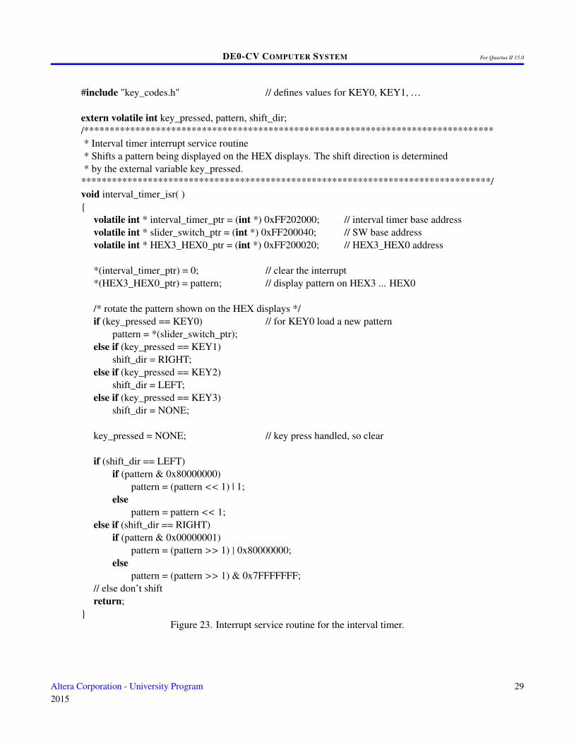
#include "key_codes.h" // defines values for KEY0, KEY1, . . .
extern volatile int key_pressed, pattern, shift_dir;/********************************************************************************* Interval timer interrupt service routine* Shifts a pattern being displayed on the HEX displays. The shift direction is determined* by the external variable key_pressed.
********************************************************************************/void interval_timer_isr( ){
volatile int * interval_timer_ptr = (int *) 0xFF202000; // interval timer base addressvolatile int * slider_switch_ptr = (int *) 0xFF200040; // SW base addressvolatile int * HEX3_HEX0_ptr = (int *) 0xFF200020; // HEX3_HEX0 address
*(interval_timer_ptr) = 0; // clear the interrupt*(HEX3_HEX0_ptr) = pattern; // display pattern on HEX3 ... HEX0
/* rotate the pattern shown on the HEX displays */if (key_pressed == KEY0) // for KEY0 load a new pattern
pattern = *(slider_switch_ptr);else if (key_pressed == KEY1)
shift_dir = RIGHT;else if (key_pressed == KEY2)
shift_dir = LEFT;else if (key_pressed == KEY3)
shift_dir = NONE;
key_pressed = NONE; // key press handled, so clear
if (shift_dir == LEFT)if (pattern & 0x80000000)
pattern = (pattern << 1) | 1;else
pattern = pattern << 1;else if (shift_dir == RIGHT)
if (pattern & 0x00000001)pattern = (pattern >> 1) | 0x80000000;
elsepattern = (pattern >> 1) & 0x7FFFFFFF;
// else don’t shiftreturn;
}Figure 23. Interrupt service routine for the interval timer.
Altera Corporation - University Program2015
29
DE0-CV COMPUTER SYSTEM For Quartus II 15.0
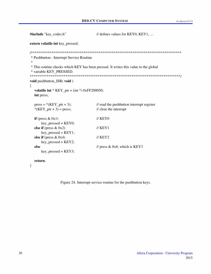
#include "key_codes.h" // defines values for KEY0, KEY1, . . .
extern volatile int key_pressed;
/********************************************************************************* Pushbutton - Interrupt Service Routine** This routine checks which KEY has been pressed. It writes this value to the global* variable KEY_PRESSED.
********************************************************************************/void pushbutton_ISR( void ){
volatile int * KEY_ptr = (int *) 0xFF200050;int press;
press = *(KEY_ptr + 3); // read the pushbutton interrupt register*(KEY_ptr + 3) = press; // clear the interrupt
if (press & 0x1) // KEY0key_pressed = KEY0;
else if (press & 0x2) // KEY1key_pressed = KEY1;
else if (press & 0x4) // KEY2key_pressed = KEY2;
else // press & 0x8, which is KEY3key_pressed = KEY3;
return;}
Figure 24. Interrupt service routine for the pushbutton keys.
30 Altera Corporation - University Program2015

DE0-CV COMPUTER SYSTEM For Quartus II 15.0
4 Media Components
This section describes the video-out and PS/2 ports.
4.1 Video-out Port
The DE0-CV Computer includes a video-out port with a VGA controller that can be connected to a standard VGAmonitor. The VGA controller supports a screen resolution of 640 × 480. The image that is displayed by the VGAcontroller is derived from two sources: a pixel buffer, and a character buffer.
4.1.1 Pixel Buffer
The pixel buffer for the video-out port reads stored pixel values from a memory buffer for display by the VGAcontroller. As illustrated in Figure 25, the memory buffer provides an image resolution of 320 × 240 pixels, with thecoordinate 0,0 being at the top-left corner of the image. Since the VGA controller supports the screen resolution of640 × 480, each of the pixel values in the pixel buffer is replicated in both the x and y dimensions when it is beingdisplayed on the VGA screen.
3190
. . .
1 2 3
. . .
. . .
. . .
. . .
012
. . .
239
Figure 25. Pixel buffer coordinates.
Figure 26a shows that each pixel value is represented as a 16-bit halfword, with five bits for the blue and redcomponents, and six bits for green. As depicted in part b of Figure 26, pixels are addressed in the memory buffer byusing the combination of a base address and an x,y offset. In the DE0-CV Computer the pixel buffer uses the baseaddress (08000000)16, which corresponds to the starting address of the FPGA on-chip memory. Using this scheme,the pixel at location 0,0 has the address (08000000)16, the pixel 1,0 has the address base + (00000000 000000001 0)2
= (08000002)16, the pixel 0,1 has the address base + (00000001 000000000 0)2 = (08000400)16, and the pixel atlocation 319,239 has the address base + (11101111 100111111 0)2 = (0803BE7E)16.
You can create an image by writing color values into the pixel addresses as described above. A dedicated pixel buffercontroller continuously reads this pixel data from sequential addresses in the corresponding memory for display onthe VGA screen. You can modify the pixel data at any time, simply by writing to the pixel addresses. Thus, animage can be changed even when it is in the process of being displayed. However, it is also possible to avoid makingchanges to the pixel buffer while it is being displayed, by using the concept of double-buffering. In this scheme, two
Altera Corporation - University Program2015
31
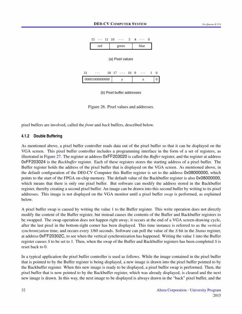
DE0-CV COMPUTER SYSTEM For Quartus II 15.0
31 . . . 1. . .1017
00001000000000
918
xy
. . .
(a) Pixel values
(b) Pixel buffer addresses
0
0
15 . . . 0. . .510
red
411
bluegreen
. . .
Figure 26. Pixel values and addresses.
pixel buffers are involved, called the front and back buffers, described below.
4.1.2 Double Buffering
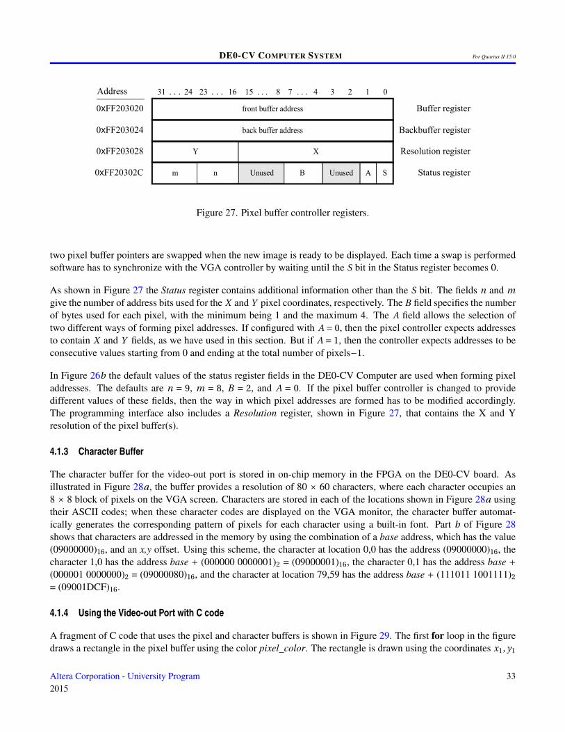
As mentioned above, a pixel buffer controller reads data out of the pixel buffer so that it can be displayed on theVGA screen. This pixel buffer controller includes a programming interface in the form of a set of registers, asillustrated in Figure 27. The register at address 0xFF203020 is called the Buffer register, and the register at address0xFF203024 is the Backbuffer register. Each of these registers stores the starting address of a pixel buffer. TheBuffer register holds the address of the pixel buffer that is displayed on the VGA screen. As mentioned above, inthe default configuration of the DE0-CV Computer this Buffer register is set to the address 0x08000000, whichpoints to the start of the FPGA on-chip memory. The default value of the Backbuffer register is also 0x08000000,which means that there is only one pixel buffer. But software can modify the address stored in the Backbufferregister, thereby creating a second pixel buffer. An image can be drawn into this second buffer by writing to its pixeladdresses. This image is not displayed on the VGA monitor until a pixel buffer swap is performed, as explainedbelow.
A pixel buffer swap is caused by writing the value 1 to the Buffer register. This write operation does not directlymodify the content of the Buffer register, but instead causes the contents of the Buffer and Backbuffer registers tobe swapped. The swap operation does not happen right away; it occurs at the end of a VGA screen-drawing cycle,after the last pixel in the bottom-right corner has been displayed. This time instance is referred to as the verticalsynchronization time, and occurs every 1/60 seconds. Software can poll the value of the S bit in the Status register,at address 0xFF20302C, to see when the vertical synchronization has happened. Writing the value 1 into the Bufferregister causes S to be set to 1. Then, when the swap of the Buffer and Backbuffer registers has been completed S isreset back to 0.
In a typical application the pixel buffer controller is used as follows. While the image contained in the pixel bufferthat is pointed to by the Buffer register is being displayed, a new image is drawn into the pixel buffer pointed to bythe Backbuffer register. When this new image is ready to be displayed, a pixel buffer swap is performed. Then, thepixel buffer that is now pointed to by the Backbuffer register, which was already displayed, is cleared and the nextnew image is drawn. In this way, the next image to be displayed is always drawn in the “back” pixel buffer, and the
32 Altera Corporation - University Program2015
DE0-CV COMPUTER SYSTEM For Quartus II 15.0
Address 01531 . . .
0xFF203020
0xFF203024
. . .
A S
1
XY
16 223
front buffer address
0xFF203028
back buffer address
0xFF20302C
3
B
. . .7
m n
48. . .24
Backbuffer register
Resolution register
Status register
Buffer register
Unused Unused
Figure 27. Pixel buffer controller registers.
two pixel buffer pointers are swapped when the new image is ready to be displayed. Each time a swap is performedsoftware has to synchronize with the VGA controller by waiting until the S bit in the Status register becomes 0.
As shown in Figure 27 the Status register contains additional information other than the S bit. The fields n and mgive the number of address bits used for the X and Y pixel coordinates, respectively. The B field specifies the numberof bytes used for each pixel, with the minimum being 1 and the maximum 4. The A field allows the selection oftwo different ways of forming pixel addresses. If configured with A = 0, then the pixel controller expects addressesto contain X and Y fields, as we have used in this section. But if A = 1, then the controller expects addresses to beconsecutive values starting from 0 and ending at the total number of pixels−1.
In Figure 26b the default values of the status register fields in the DE0-CV Computer are used when forming pixeladdresses. The defaults are n = 9, m = 8, B = 2, and A = 0. If the pixel buffer controller is changed to providedifferent values of these fields, then the way in which pixel addresses are formed has to be modified accordingly.The programming interface also includes a Resolution register, shown in Figure 27, that contains the X and Yresolution of the pixel buffer(s).
4.1.3 Character Buffer
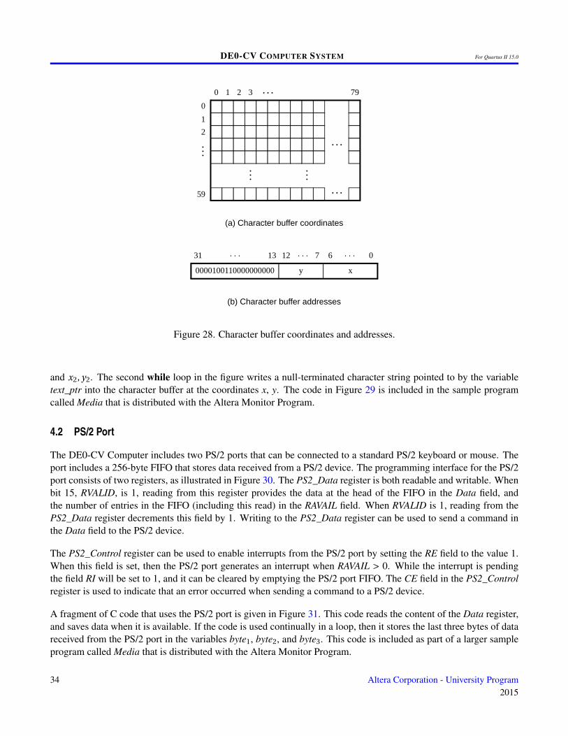
The character buffer for the video-out port is stored in on-chip memory in the FPGA on the DE0-CV board. Asillustrated in Figure 28a, the buffer provides a resolution of 80 × 60 characters, where each character occupies an8 × 8 block of pixels on the VGA screen. Characters are stored in each of the locations shown in Figure 28a usingtheir ASCII codes; when these character codes are displayed on the VGA monitor, the character buffer automat-ically generates the corresponding pattern of pixels for each character using a built-in font. Part b of Figure 28shows that characters are addressed in the memory by using the combination of a base address, which has the value(09000000)16, and an x,y offset. Using this scheme, the character at location 0,0 has the address (09000000)16, thecharacter 1,0 has the address base + (000000 0000001)2 = (09000001)16, the character 0,1 has the address base +(000001 0000000)2 = (09000080)16, and the character at location 79,59 has the address base + (111011 1001111)2
= (09001DCF)16.
4.1.4 Using the Video-out Port with C code
A fragment of C code that uses the pixel and character buffers is shown in Figure 29. The first for loop in the figuredraws a rectangle in the pixel buffer using the color pixel_color. The rectangle is drawn using the coordinates x1, y1
Altera Corporation - University Program2015
33
DE0-CV COMPUTER SYSTEM For Quartus II 15.0
790
. . .
1 2 3
. . .
. . .
. . .
. . .
012
. . .
59
31 . . . 0. . .712
0000100110000000000
613
xy
. . .
(a) Character buffer coordinates
(b) Character buffer addresses
Figure 28. Character buffer coordinates and addresses.
and x2, y2. The second while loop in the figure writes a null-terminated character string pointed to by the variabletext_ptr into the character buffer at the coordinates x, y. The code in Figure 29 is included in the sample programcalled Media that is distributed with the Altera Monitor Program.
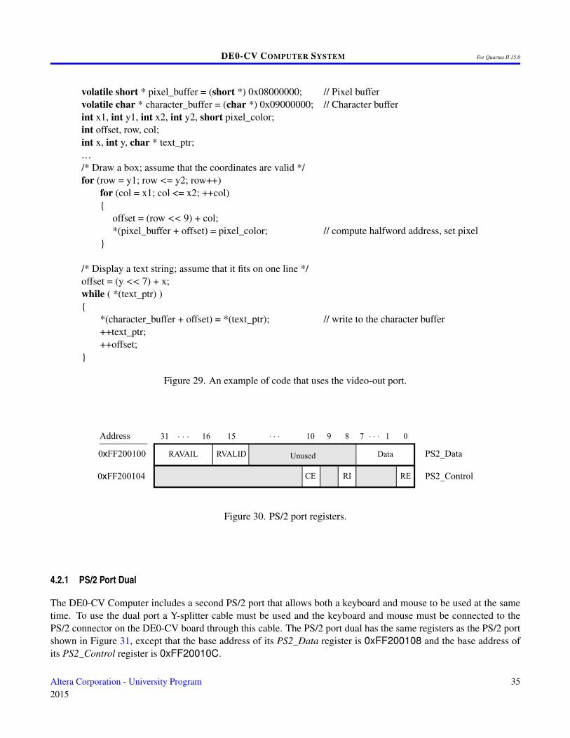
4.2 PS/2 Port
The DE0-CV Computer includes two PS/2 ports that can be connected to a standard PS/2 keyboard or mouse. Theport includes a 256-byte FIFO that stores data received from a PS/2 device. The programming interface for the PS/2port consists of two registers, as illustrated in Figure 30. The PS2_Data register is both readable and writable. Whenbit 15, RVALID, is 1, reading from this register provides the data at the head of the FIFO in the Data field, andthe number of entries in the FIFO (including this read) in the RAVAIL field. When RVALID is 1, reading from thePS2_Data register decrements this field by 1. Writing to the PS2_Data register can be used to send a command inthe Data field to the PS/2 device.
The PS2_Control register can be used to enable interrupts from the PS/2 port by setting the RE field to the value 1.When this field is set, then the PS/2 port generates an interrupt when RAVAIL > 0. While the interrupt is pendingthe field RI will be set to 1, and it can be cleared by emptying the PS/2 port FIFO. The CE field in the PS2_Controlregister is used to indicate that an error occurred when sending a command to a PS/2 device.
A fragment of C code that uses the PS/2 port is given in Figure 31. This code reads the content of the Data register,and saves data when it is available. If the code is used continually in a loop, then it stores the last three bytes of datareceived from the PS/2 port in the variables byte1, byte2, and byte3. This code is included as part of a larger sampleprogram called Media that is distributed with the Altera Monitor Program.
34 Altera Corporation - University Program2015
DE0-CV COMPUTER SYSTEM For Quartus II 15.0
volatile short * pixel_buffer = (short *) 0x08000000; // Pixel buffervolatile char * character_buffer = (char *) 0x09000000; // Character bufferint x1, int y1, int x2, int y2, short pixel_color;int offset, row, col;int x, int y, char * text_ptr;. . ./* Draw a box; assume that the coordinates are valid */for (row = y1; row <= y2; row++)
for (col = x1; col <= x2; ++col){
offset = (row << 9) + col;*(pixel_buffer + offset) = pixel_color; // compute halfword address, set pixel
}
/* Display a text string; assume that it fits on one line */offset = (y << 7) + x;while ( *(text_ptr) ){
*(character_buffer + offset) = *(text_ptr); // write to the character buffer++text_ptr;++offset;
}
Figure 29. An example of code that uses the video-out port.
Address 01531 . . .
0xFF200100
0xFF200104
. . .
Unused
RE
1
DataRAVAIL
16
PS2_Data
RI
. . .89
CE
710
PS2_Control
RVALID
Figure 30. PS/2 port registers.
4.2.1 PS/2 Port Dual
The DE0-CV Computer includes a second PS/2 port that allows both a keyboard and mouse to be used at the sametime. To use the dual port a Y-splitter cable must be used and the keyboard and mouse must be connected to thePS/2 connector on the DE0-CV board through this cable. The PS/2 port dual has the same registers as the PS/2 portshown in Figure 31, except that the base address of its PS2_Data register is 0xFF200108 and the base address ofits PS2_Control register is 0xFF20010C.
Altera Corporation - University Program2015
35
DE0-CV COMPUTER SYSTEM For Quartus II 15.0
volatile int * PS2_ptr = (int *) 0xFF200100; // PS/2 port addressint PS2_data, RVALID;char byte1 = 0, byte2 = 0, byte3 = 0;. . .PS2_data = *(PS2_ptr); // read the Data register in the PS/2 portRVALID = PS2_data & 0x8000; // extract the RVALID fieldif (RVALID){
/* save the last three bytes of data */byte1 = byte2;byte2 = byte3;byte3 = PS2_data & 0xFF;
}. . .
Figure 31. An example of code that uses the PS/2 port.
4.3 Floating-point Hardware
The Nios II processor in the DE0-CV Computer includes hardware support for floating-point addition, subtraction,multiplication, and division. To use this support in a C program, variables must be declared with the type float. Asimple example of such code is given in Figure 32. When this code is compiled, it is necessary to pass the specialargument -mcustom-fpu-cfg=60-2 to the C compiler, to instruct it to use the floating-point hardware support.
5 Modifying the DE0-CV Computer
It is possible to modify the DE0-CV Computer by using Altera’s Quartus II software and Qsys tool. Tutorials thatintroduce this software are provided in the University Program section of Altera’s web site. To modify the system itis first necessary to make an editable copy of the DE0-CV Computer. The files for this system are installed as part ofthe Monitor Program installation. Locate these files, copy them to a working directory, and then use the Quartus IIand Qsys software to make any desired changes.
6 Making the System the Default Configuration
The DE0-CV Computer can be loaded into the nonvolatile FPGA configuration memory on the DE0-CV board, sothat it becomes the default system whenever the board is powered on. Instructions for configuring the DE0-CV boardin this manner can be found in the tutorial Introduction to the Quartus II Software, which is available from Altera’sUniversity Program.
36 Altera Corporation - University Program2015
DE0-CV COMPUTER SYSTEM For Quartus II 15.0
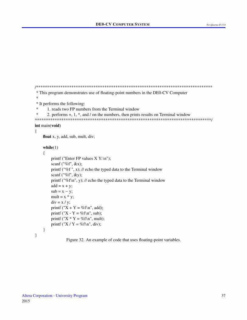
/********************************************************************************* This program demonstrates use of floating-point numbers in the DE0-CV Computer** It performs the following:* 1. reads two FP numbers from the Terminal window* 2. performs +, 1, *, and / on the numbers, then prints results on Terminal window
********************************************************************************/int main(void){
float x, y, add, sub, mult, div;
while(1){
printf ("Enter FP values X Y:\n");scanf ("%f", &x);printf ("%f ", x); // echo the typed data to the Terminal windowscanf ("%f", &y);printf ("%f\n", y); // echo the typed data to the Terminal windowadd = x + y;sub = x − y;mult = x * y;div = x / y;printf ("X + Y = %f\n", add);printf ("X - Y = %f\n", sub);printf ("X * Y = %f\n", mult);printf ("X / Y = %f\n", div);
}}
Figure 32. An example of code that uses floating-point variables.
Altera Corporation - University Program2015
37
DE0-CV COMPUTER SYSTEM For Quartus II 15.0
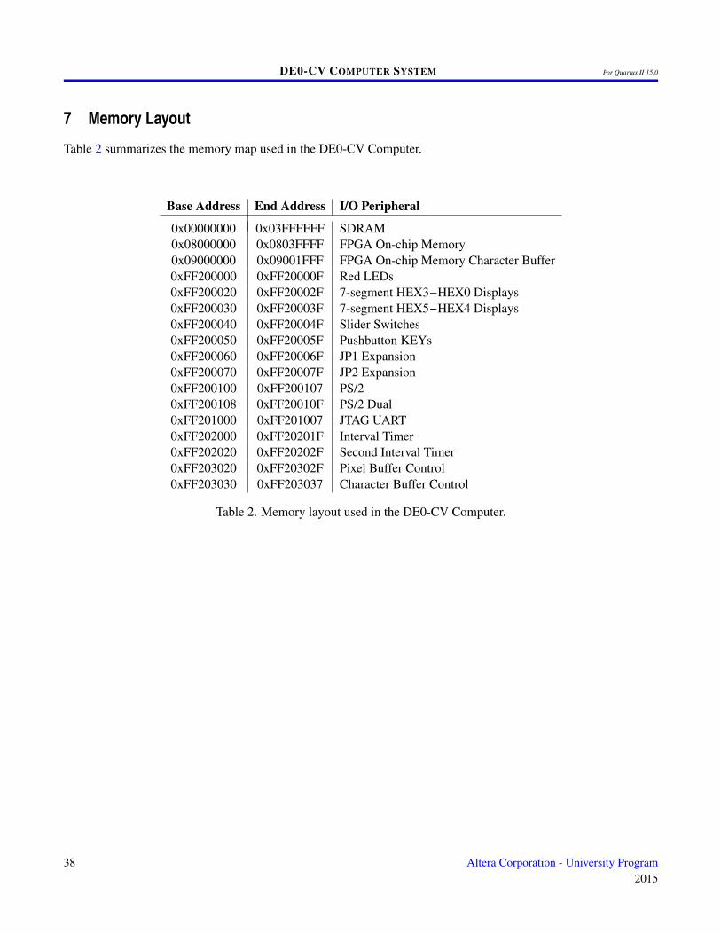
7 Memory Layout
Table 2 summarizes the memory map used in the DE0-CV Computer.
Base Address End Address I/O Peripheral
0x00000000 0x03FFFFFF SDRAM0x08000000 0x0803FFFF FPGA On-chip Memory0x09000000 0x09001FFF FPGA On-chip Memory Character Buffer0xFF200000 0xFF20000F Red LEDs0xFF200020 0xFF20002F 7-segment HEX3−HEX0 Displays0xFF200030 0xFF20003F 7-segment HEX5−HEX4 Displays0xFF200040 0xFF20004F Slider Switches0xFF200050 0xFF20005F Pushbutton KEYs0xFF200060 0xFF20006F JP1 Expansion0xFF200070 0xFF20007F JP2 Expansion0xFF200100 0xFF200107 PS/20xFF200108 0xFF20010F PS/2 Dual0xFF201000 0xFF201007 JTAG UART0xFF202000 0xFF20201F Interval Timer0xFF202020 0xFF20202F Second Interval Timer0xFF203020 0xFF20302F Pixel Buffer Control0xFF203030 0xFF203037 Character Buffer Control
Table 2. Memory layout used in the DE0-CV Computer.
38 Altera Corporation - University Program2015
DE0-CV COMPUTER SYSTEM For Quartus II 15.0
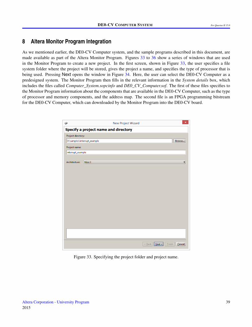
8 Altera Monitor Program Integration
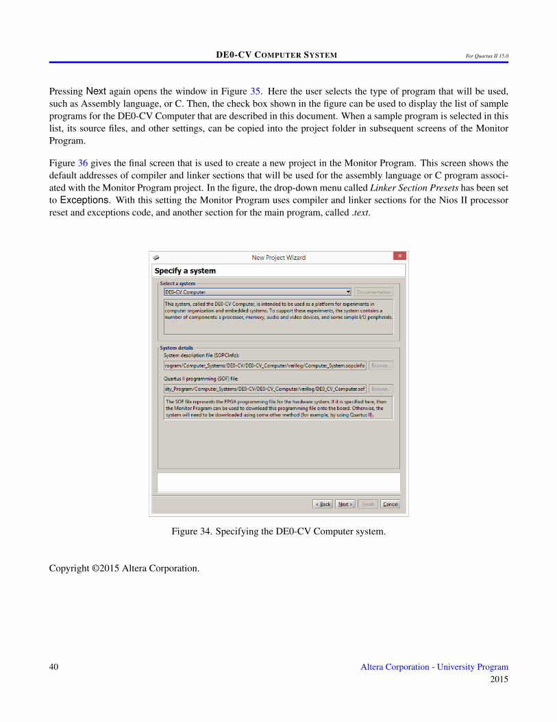
As we mentioned earlier, the DE0-CV Computer system, and the sample programs described in this document, aremade available as part of the Altera Monitor Program. Figures 33 to 36 show a series of windows that are usedin the Monitor Program to create a new project. In the first screen, shown in Figure 33, the user specifies a filesystem folder where the project will be stored, gives the project a name, and specifies the type of processor that isbeing used. Pressing Next opens the window in Figure 34. Here, the user can select the DE0-CV Computer as apredesigned system. The Monitor Program then fills in the relevant information in the System details box, whichincludes the files called Computer_System.sopcinfo and DE0_CV_Computer.sof. The first of these files specifies tothe Monitor Program information about the components that are available in the DE0-CV Computer, such as the typeof processor and memory components, and the address map. The second file is an FPGA programming bitstreamfor the DE0-CV Computer, which can downloaded by the Monitor Program into the DE0-CV board.
Figure 33. Specifying the project folder and project name.
Altera Corporation - University Program2015
39
DE0-CV COMPUTER SYSTEM For Quartus II 15.0
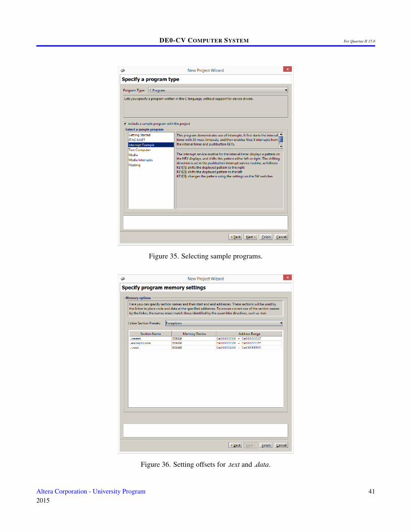
Pressing Next again opens the window in Figure 35. Here the user selects the type of program that will be used,such as Assembly language, or C. Then, the check box shown in the figure can be used to display the list of sampleprograms for the DE0-CV Computer that are described in this document. When a sample program is selected in thislist, its source files, and other settings, can be copied into the project folder in subsequent screens of the MonitorProgram.
Figure 36 gives the final screen that is used to create a new project in the Monitor Program. This screen shows thedefault addresses of compiler and linker sections that will be used for the assembly language or C program associ-ated with the Monitor Program project. In the figure, the drop-down menu called Linker Section Presets has been setto Exceptions. With this setting the Monitor Program uses compiler and linker sections for the Nios II processorreset and exceptions code, and another section for the main program, called .text.
Figure 34. Specifying the DE0-CV Computer system.
Copyright ©2015 Altera Corporation.
40 Altera Corporation - University Program2015
DE0-CV COMPUTER SYSTEM For Quartus II 15.0
Figure 35. Selecting sample programs.
Figure 36. Setting offsets for .text and .data.
Altera Corporation - University Program2015
41