(DDR3) SDRAM Controller IP Core User's Guide
61
Double Data Rate (DDR3) SDRAM Controller IP Core User Guide IPUG80 Version 1.9, October 2016
Transcript of (DDR3) SDRAM Controller IP Core User's Guide

Double Data Rate (DDR3) SDRAM Controller IP Core User Guide
IPUG80 Version 1.9, October 2016
© 2016 Lattice Semiconductor Corp. All Lattice trademarks, registered trademarks, patents, and disclaimers are as listed at www.latticesemi.com/legal. All other brand or product names are trademarks or registered trademarks of their respective holders. The specifications and information herein are subject to change without notice.
IPUG80_1.9, October 2016 2 DDR3 SDRAM Controller IP Core User’s Guide
Chapter 1. Introduction .......................................................................................................................... 5Quick Facts ........................................................................................................................................................... 5Features ................................................................................................................................................................ 6
Chapter 2. Functional Description ........................................................................................................ 8Overview ............................................................................................................................................................... 8DDR3 MC Module ................................................................................................................................................. 9
Command Decode Logic.............................................................................................................................. 9Command Application Logic ........................................................................................................................ 9On-Die Termination...................................................................................................................................... 9
DDR3 PHY Module ............................................................................................................................................... 9Initialization Module............................................................................................................................................. 10
Write Leveling ............................................................................................................................................ 10Read Training (Only for ECP5 Device) ...................................................................................................... 10
Selecting READ_PULSE_TAP Value (Only for LatticeECP3 Device) ................................................................ 11Data Path Logic.......................................................................................................................................... 11
Signal Descriptions ............................................................................................................................................. 11Using the Local User Interface............................................................................................................................ 14
Initialization Control.................................................................................................................................... 14Command and Address ............................................................................................................................. 15User Commands ........................................................................................................................................ 16WRITE........................................................................................................................................................ 16WRITEA ..................................................................................................................................................... 17READ ......................................................................................................................................................... 17READA....................................................................................................................................................... 18REFRESH Support .................................................................................................................................... 18
Local-to-Memory Address Mapping .................................................................................................................... 19Mode Register Programming .............................................................................................................................. 19
Chapter 3. Parameter Settings ............................................................................................................ 21Type Tab ............................................................................................................................................................. 23
Select Memory ........................................................................................................................................... 24RefClock (Only for ECP5 DDR3 IP) ........................................................................................................... 24Clock (for ECP3) MemClock (for ECP5) .................................................................................................... 24Memory Type ............................................................................................................................................. 24Memory Data Bus Size .............................................................................................................................. 24Configuration.............................................................................................................................................. 24DIMM Type or Chip Select Width............................................................................................................... 24Address Mirror............................................................................................................................................ 24Clock Width ................................................................................................................................................ 24CKE Width.................................................................................................................................................. 252T MODE ................................................................................................................................................... 25Data_rdy to Write Data Delay .................................................................................................................... 25Write Leveling ............................................................................................................................................ 25Controller Reset to Memory ....................................................................................................................... 25
Setting Tab.......................................................................................................................................................... 25Row Size .................................................................................................................................................... 26Column Size............................................................................................................................................... 26Auto Refresh Burst Count .......................................................................................................................... 26External Auto Refresh Port ........................................................................................................................ 26Burst Length............................................................................................................................................... 26
Table of Contents

Table of Contents
IPUG80_1.9, October 2016 3 DDR3 SDRAM Controller IP Core User’s Guide
CAS Latency .............................................................................................................................................. 26Burst Type.................................................................................................................................................. 26Write Recovery........................................................................................................................................... 26DLL Control for PD..................................................................................................................................... 26ODI Control ................................................................................................................................................ 26RTT_Nom................................................................................................................................................... 26Additive Latency......................................................................................................................................... 26CAS Write Latency..................................................................................................................................... 27RTT_WR .................................................................................................................................................... 27
Memory Device Timing Tab ................................................................................................................................ 27Manually Adjust.......................................................................................................................................... 28tCLK - Memory clock.................................................................................................................................. 28Command and Address Timing.................................................................................................................. 28Calibration Timing ...................................................................................................................................... 28Refresh, Reset and Power Down Timing ................................................................................................... 28Write Leveling Timing................................................................................................................................. 28
Pin Selection Tab ................................................................................................................................................ 29Manually Adjust.......................................................................................................................................... 29Pin Side...................................................................................................................................................... 29clk_in/PLL Locations .................................................................................................................................. 30clk_in pin .................................................................................................................................................... 30PLL Used ................................................................................................................................................... 30
DDR3 SDRAM Memory Clock Pin Location........................................................................................................ 30em_ddr_clk................................................................................................................................................. 30DQS Locations........................................................................................................................................... 30
Design Tools Options and Info Tab..................................................................................................................... 31Support Synplify ......................................................................................................................................... 31Support ModelSim...................................................................................................................................... 31Support ALDEC.......................................................................................................................................... 31Memory I/F Pins ......................................................................................................................................... 31User I/F Pins .............................................................................................................................................. 32
Chapter 4. IP Core Generation and Evaluation for LatticeECP3 DDR3 ........................................... 33Getting Started .................................................................................................................................................... 33IPexpress-Created Files and Top Level Directory Structure............................................................................... 35
DDR3 Memory Controller IP File Structure ................................................................................................ 37Simulation Files for IP Evaluation .............................................................................................................. 38
Hardware Evaluation........................................................................................................................................... 39Enabling Hardware Evaluation in Diamond................................................................................................ 39
Updating/Regenerating the IP Core .................................................................................................................... 40Chapter 5. IP Core Generation and Evaluation for ECP5 DDR3 ....................................................... 41
Getting Started .................................................................................................................................................... 41Created Files and Top Level Directory Structure ................................................................................................ 44
DDR3 Memory Controller IP File Structure ................................................................................................ 46Simulation Files for IP Evaluation .............................................................................................................. 47
Hardware Evaluation........................................................................................................................................... 49Enabling Hardware Evaluation in Diamond:............................................................................................... 49
Regenerating/Recreating the IP Core ................................................................................................................. 49Regenerating an IP Core in Clarity Designer Tool ..................................................................................... 49Recreating an IP Core in Clarity Designer Tool ......................................................................................... 49
Chapter 6. Application Support........................................................................................................... 50Understanding Preferences ................................................................................................................................ 50
FREQUENCY Preferences ........................................................................................................................ 50MAXDELAY NET ....................................................................................................................................... 50
Table of Contents
IPUG80_1.9, October 2016 4 DDR3 SDRAM Controller IP Core User’s Guide
MULTICYCLE / BLOCK PATH................................................................................................................... 50IOBUF ........................................................................................................................................................ 50LOCATE..................................................................................................................................................... 50
Handling DDR3 IP Preferences in User Designs ................................................................................................ 50Reset Handling.................................................................................................................................................... 51Dummy Logic Removal ....................................................................................................................................... 51Top-level Wrapper File Only for Evaluation Implementation............................................................................... 51Top-level Wrapper file for All Simulation Cases and Implementation in a User’s Design ................................... 51RDIMM Module Support...................................................................................................................................... 52
Chapter 7. Core Validation................................................................................................................... 53Chapter 8. Support Resources ............................................................................................................ 54
Lattice Technical Support.................................................................................................................................... 54References.......................................................................................................................................................... 54Revision History .................................................................................................................................................. 54
Appendix A. Resource Utilization ....................................................................................................... 56ECP5 Devices ..................................................................................................................................................... 56
Ordering Part Number................................................................................................................................ 56LatticeECP3 Devices .......................................................................................................................................... 57
Ordering Part Number................................................................................................................................ 57Appendix B. Lattice Device Versus DDR3 IP Matrix ......................................................................................................................... 58Appendix C. Lattice ECP3 DDR3 IP Locate Constraints ................................................................................................................ 59
IPUG80_1.9, October 2016 5 DDR3 SDRAM Controller IP Core User’s Guide
The Lattice Double Data Rate (DDR3) Synchronous Dynamic Random Access Memory (SDRAM) Controller is a general-purpose memory controller that interfaces with industry standard DDR3 memory devices/modules compli-ant with JESD79-3, DDR3 SDRAM Standard, and provides a generic command interface to user applications. The DDR3 SDRAM is the next-generation DDR SDRAM memory technology which features faster speed, mitigated SSO, and reduced routing due to “fly-by” routing signals to SDRAM instead of low skew tree distribution. This core reduces the effort required to integrate the DDR3 memory controller with the remainder of the application and min-imizes the need to directly deal with the DDR3 memory interface.
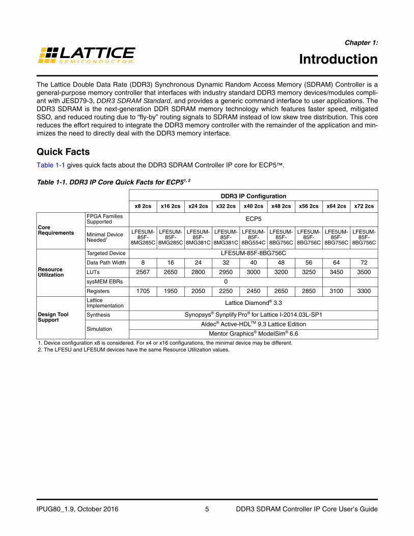
Quick FactsTable 1-1 gives quick facts about the DDR3 SDRAM Controller IP core for ECP5™.
Table 1-1. DDR3 IP Core Quick Facts for ECP51, 2
DDR3 IP Configuration
x8 2cs x16 2cs x24 2cs x32 2cs x40 2cs x48 2cs x56 2cs x64 2cs x72 2cs
Core Requirements
FPGA Families Supported ECP5
Minimal Device Needed1
LFE5UM-85F-
8MG285C
LFE5UM-85F-
8MG285C
LFE5UM-85F-
8MG381C
LFE5UM-85F-
8MG381C
LFE5UM-85F-
8BG554C
LFE5UM-85F-
8BG756C
LFE5UM-85F-
8BG756C
LFE5UM-85F-
8BG756C
LFE5UM-85F-
8BG756C
Resource Utilization
Targeted Device LFE5UM-85F-8BG756C
Data Path Width 8 16 24 32 40 48 56 64 72
LUTs 2567 2650 2800 2950 3000 3200 3250 3450 3500
sysMEM EBRs 0
Registers 1705 1950 2050 2250 2450 2650 2850 3100 3300
Design Tool Support
Lattice Implementation Lattice Diamond® 3.3
Synthesis Synopsys® Synplify Pro® for Lattice I-2014.03L-SP1
SimulationAldec® Active-HDLTM 9.3 Lattice Edition
Mentor Graphics® ModelSim® 6.6
1. Device configuration x8 is considered. For x4 or x16 configurations, the minimal device may be different.2. The LFE5U and LFE5UM devices have the same Resource Utilization values.
Chapter 1:
Introduction

Introduction
IPUG80_1.9, October 2016 6 DDR3 SDRAM Controller IP Core User’s Guide
Table 1-2 gives quick facts about the DDR3 SDRAM Controller IP core for LatticeECP3™.
FeaturesThe DDR3 SDRAM Controller IP core supports the following features:
• Support for all ECP5 devices (LFE5U/LFE5UM) and all LatticeECP3 “EA” devices
• Interfaces to industry standard DDR3 SDRAM components and modules compliant with JESD79-3, DDR3 SDRAM Standard
• Interfaces to DDR3 SDRAM at speeds up to 400 MHz / 800 Mbps in -9 speed grade ECP5 devices and -8 speed grade LatticeECP3 devices
• Supports memory data path widths of -8, -16, -24, -32, -40, -48, -56, -64 and -72 bits
• Supports x4, x8, and x16 device configurations
• Supports a single UDIMM or RDIMM DDR3 module
• Supports one DIMM and up to two ranks per DIMM (up to two chip select).
• Programmable burst lengths of 8 (fixed), chopped 4 or 8 (on-the-fly), or chopped 4 (fixed)
• Programmable CAS latency
• Programmable CAS write latency
• Read burst type of nibble sequential or interleave
• Supports automatic DDR3 SDRAM initialization and refresh
• Automatic write leveling for each DQS for DIMM applications. Option to switch off write leveling for on-board memory applications.
• Automatic read training for each DQS
• Supports Power Down Mode
Table 1-2. DDR3 IP Core Quick Facts for LatticeECP3
DDR3 IP Configuration
x8 2cs x16 2cs x24 2cs x32 2cs x40 2cs x48 2cs x56 2cs x64 2cs x72 2cs
Core Requirements
FPGA Families Supported LatticeECP3
Minimal Device Needed
LFE3-17EA-6FTN256C
LFE3- 17EA-6FTN256C
LFE3- 17EA-6MG328C
LFE3- 17EA-6FN484C
LFE3- 17EA-6FN484C
LFE3- 35EA-
6FN484C
LFE3- 35EA-
6FN672C
LFE3- 70EA-
6FN672C
LFE3- 70EA-
6FN1156C
Resource Utilization
Targeted Device LFE3-150EA-8FN1156C
Data Path Width 8 16 24 32 40 48 56 64 72
LUTs 2519 2661 2820 2934 2890 2968 3080 3212 3348
sysMEM EBRs 0
Registers 1764 2129 2467 2803 2685 2886 3112 3320 3469
Design Tool Support
Lattice Implementation Lattice Diamond® 3.3
Synthesis Synopsys® Synplify® Pro for Lattice I-2014.03L-SP1
SimulationAldec® Active-HDL® 9.3 SP1 Lattice Edition
Mentor Graphics® ModelSim® 6.6

Introduction
IPUG80_1.9, October 2016 7 DDR3 SDRAM Controller IP Core User’s Guide
• Supports Dynamic On-Die Termination (ODT) controls
• Termination Data Strobe (TDQS) for x8 widths only
• I/O primitives manage read skews (read leveling equivalent)
• Automatic programmable interval refresh or user initiated refresh
• Option for controlling memory reset outside the controller
IPUG80_1.9, October 2016 8 DDR3 SDRAM Controller IP Core User’s Guide
This chapter provides a functional description of the DDR3 SDRAM Controller IP core.
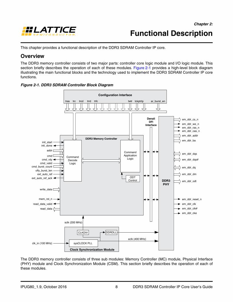
OverviewThe DDR3 memory controller consists of two major parts: controller core logic module and I/O logic module. This section briefly describes the operation of each of these modules. Figure 2-1 provides a high-level block diagram illustrating the main functional blocks and the technology used to implement the DDR3 SDRAM Controller IP core functions.
Figure 2-1. DDR3 SDRAM Controller Block Diagram
The DDR3 memory controller consists of three sub modules: Memory Controller (MC) module, Physical Interface (PHY) module and Clock Synchronization Module (CSM). This section briefly describes the operation of each of these modules.
cmd
addr
cmd_rdy
read_data
inti_done
CommandDecodeLogic
CommandApplication
Logic
em_ddr_cke
em_ddr_we_nem_ddr_ras_nem_ddr_cas_n
em_ddr_addr
em_ddr_ba
em_ddr_dm
sysCLOCK PLLclk_in (100 MHz)
cmd_valid
init_start
cmd_burst_count
read_data_valid
em_ddr_dq
em_ddr_dqs
em_ddr_cs_n
em_ddr_odt
DDR3 Memory Controller
ofly_burst_len
DDRDLL
em_ddr_clk#
em_ddr_clk
em_ddr_dqs#
eclk (400 MHz)
write_data
sclk (200 MHz)
ext_auto_ref_ack
ext_auto_ref
Configuration Interface
ar_burst_enrtwtcfrtdrrtdcrtcrtsart tckptrtp
ODTControl
Clock Synchronization Module
mem_rst_n em_ddr_reset_n
DenaliDFI
Interface
CLKDIV
DDR3PHY
Chapter 2:
Functional Description

Functional Description
IPUG80_1.9, October 2016 9 DDR3 SDRAM Controller IP Core User’s Guide
The DDR3 MC module has the following functional sub-modules: Command Decode Logic (CDL) block, Command Application Logic (CAL) block and ODT Control block.
The DDR3 PHY modules provide the PHY interface to the memory device. This block mostly consists of LatticeECP3 or ECP5 device DDR I/O primitives supporting compliance to DDR3 electrical and timing require-ments. In addition, this module consists of the logic for memory initialization, write leveling, read training and write/read data path.
Along with the DDR3 SDRAM Controller IP core, a separate module, called the Clock Synchronization Module (CSM), is also provided. The CSM generates all the clock signals, such as system clock (SCLK) and edge clock (ECLK) for the IP core.
The CSM logic ensures that the domain crossing margin between ECLK to SCLK stays the same for the IDDR and ODDR buses that produce 2:1 gearing. Without proper synchronization, the bit order on different elements might be off-sync with each other and the entire bus is scrambled. The clock synchronization ensures that all DDR com-ponents start from exactly the same edge clock cycle.
For 400 MHz DDR3 memory clock operation, the MC module operates with a 200 MHz system clock (SCLK), the I/O logic works with a 400 MHz edge clock (ECLK). The combination of this operating clock ratio and the double data rate transfer leads to a user side data bus that is four times the width of the memory side data bus. For exam-ple, a 32-bit memory side data width requires a 128-bit read data bus and a128-bit write data bus at the user side interface.
DDR3 MC ModuleCommand Decode LogicThe Command Decode Logic (CDL) block accepts user commands from the local interface and decodes them to generate a sequence of internal memory commands depending on the current command and the status of current bank and row. The intelligent bank management logic tracks the open/close status of every bank and stores the row address of every opened bank. The controller implements a command pipeline to improve throughput. With this capability, the next command in the queue is decoded while the current command is presented at the memory interface.
Command Application LogicThe Command Application Logic (CAL) block accepts the decoded internal command sequence from the Com-mand Decode Logic and translates each sequence into memory commands that meet the operational sequence and timing requirements of the memory device. The CDL and CAL blocks work in parallel to fill and empty the com-mand queue respectively.
On-Die TerminationThe ODT feature is designed to improve the signal integrity of the memory channel by allowing the DDR3 SDRAM controller to independently turn on or turn off the termination resistance for any or all DDR3 SDRAM devices.
DDR3 PHY ModuleThe DDR3 PHY module implements soft logic in the FPGA fabric for initialization, write leveling, read training and read/write data paths, and hard logic, called DDR3 I/O modules, for 1:2 clock gearing and DDR3 memory interface. The DDR3 I/O modules are LatticeECP3 or ECP5 device hardware primitives that directly interface with the DDR3 memory. These primitives implement all of the interface signals required for memory access. They convert the sin-gle data rate (SDR) data to double rate DDR3 data for write operation and perform the DDR3 to SDR conversion in read mode.

Functional Description
IPUG80_1.9, October 2016 10 DDR3 SDRAM Controller IP Core User’s Guide
Initialization ModuleThe Initialization block performs the DDR3 memory initialization sequence as defined by JEDEC protocol. After power on or a normal reset of the DDR3 controller, memory must be initialized before sending any command to the controller. It is the user's responsibility to assert the init_start input to the DDR3 controller to start the memory ini-tialization sequence. The completion of initialization is indicated by the init_done output provided by this block.
Write LevelingThe write leveling block adjusts the DQS-to-CLK relationship for each memory device, using the write level mode of the DDR3 SDRAM when the fly-by wiring is implemented. Write leveling is always done immediately after a mem-ory initialization sequence if write leveling is not disabled through the GUI. When the init_done signal is asserted after the initialization process it also indicates the completion of write leveling. Along with the assertion of init_done, the signal wl_err is also asserted if the write leveling process is not successful.
The main purpose of write leveling is to provide better signal integrity by using fly-by topology for the address, com-mand, control and clock signals, and then by de-skewing the DQS signal delays to those signals at the DDR3 DRAM side. Since DDR3 memory modules have adapted fly-by topology, write leveling must be enabled for DIMM based applications. For on-board memory applications, the GUI provides the write leveling function as a user option. When enabled, the PCB for the on-board memory application must be routed using the fly-by topology. Oth-erwise, write leveling failures may occur due to the lack of guaranteed DQS to CLK edge relationship at the begin-ning of write level training. Due to this reason, the write leveling option must be disabled if the PCB does not utilize fly-by routing for write leveling.
The write leveling scheme of the DDR3 SDRAM Controller IP core follows all the steps stipulated in the JEDEC specification. For more details on write leveling, refer to the JEDEC specification JESD79-3.
Read Training (Only for ECP5 Device)For every read operation, the DDR3 I/O primitives of the ECP5 device must be initialized at the appropriate time to identify the incoming DQS preamble. Upon proper detection of the preamble, the primitive DQSBUFI extracts a clean dqs signal out of the incoming dqs signal from the memory and generates the DATAVALID output signal that indicates the correct timing window of the valid read data.
The memory controller generates an internal pulse signal, READ[3:0], to the primitive DQSBUFI that is used for the above-mentioned operation. In addition to the READ[3:0] input, another input signal READCLKSEL[2:0] and an output signal, BURSTDET, of the DQSBUFI block are provided to the controller to accomplish the READ signal positioning.
Due to the DQS round trip delay that includes PCB routing and I/O pad delays, proper positioning of the READ sig-nal with respect to the incoming preamble is crucial for successful read operations. The ECP5 DQSBUFI block sup-ports a dynamic READ signal positioning function called read training that enables the memory controller to position the READ signal within an appropriate timing window by progressively shifting the READ signal and moni-toring the positioning result.
This read training is performed as part of the memory initialization process after the write leveling operation is com-plete. During the read training, the memory controller generates the READ[3:0] pulse, positions this signal using READCLKSEL[2:0] and monitors the BURSTDET output of DQSBUFI for the result of the current position. The READ signal is set high before the read preamble starts. When the READ pulse is properly positioned, the pream-ble is detected correctly and the BURSTDET will go high. This will guarantee that the generated DATAVALID signal is indicating the correct read valid time window.
The READ signal is generated in the system clock (SCLK) domain and stays asserted for the total burst length of the read operation.
A minimum burst length of four on the memory bus is used in the read training process. The memory controller can determine the proper position alignment when there is not a single failure on BURSTDET assertions during the

Functional Description
IPUG80_1.9, October 2016 11 DDR3 SDRAM Controller IP Core User’s Guide
multiple trials. If there is any failure, the memory controller shifts the READ signal position and tries again until it detects no BURSTDET failure.
The memory controller stores the delay value of the successful position of the READ signal for each DQS group. It uses these delay values during a normal read operation to correctly detect the preamble first, followed by the gen-eration of DATAVALID signal.
Selecting READ_PULSE_TAP Value (Only for LatticeECP3 Device)For every read operation, the DDR3 I/O primitives must be initialized at the appropriate time to identify the incom-ing DQS preamble in order to generate the data valid signal. For this purpose the controller internally generates a signal called dqs_read in such a way that this signal’s trailing edge is positioned within the incoming DQS preamble window.
Due to PCB routing delays, DIMM module routing delays and routing delays within the FPGA, the incoming DQS signal’s delay varies from board to board. To compensate for this variability in DQS delay, the controller shifts the internal signal dqs_read in such a way to position it within the preamble time.
Each shift (step) moves the dqs_read signal by one half period of the eclk (1.25ns for 400MHz memory clock).
A port, read_pulse_tap, is provided in the Core top level file ddr3_sdram_mem_top_wrapper.v for the user to load the shift count for each DQS group. Each DQS group is assigned a 3-bit shift count value in this port, starting with LSB 3 bits for DQS_0. This count can be any value from 0 to 7.
For the core to work properly on the board, it is recommended that the dqs_read signal be shifted by two steps for UDIMMs, by four steps for RDIMMs or by one step for on-board memory. Since the Eval simulation environment is provided without the PCB and FPGA internal routing delays, the recommended values for Eval simulation are: zero steps for UDIMMs, two steps for RDIMMs or zero steps for on-board memory.
A parameter READ_PULSE_TAP in ddr_p_eval\testbench\tests\ecp3\tb_config_params.v is made available to the user as an example. This parameter may be loaded to the port read_pulse_tap with appropriate values for simula-tion and synthesis.
In almost all cases the recommended value is good enough for stable read operations on the board and it is highly unlikely that the user has to change this value. If there are frequent read errors on the board, the user should try adjusting the shift count value loaded to the port read_pulse_tap.
Should there be a need to change the READ_PULSE_TAP value, it is suggested that the user starts with changing the value of DQS7 groups first and then move to adjacent group, if required.
Note: The DDR3 memory controller may fail to generate or improperly generate the read_data_valid signal if the parameter READ_PULSE_TAP is not loaded to the read_pulse_tap input port or the values are not correct.
Data Path LogicThe Data Path Logic (DPL) block interfaces with the DDR3 I/O modules and is responsible for generating the read data and read data valid signals during read operations. This block implements all the logic needed to ensure that the data write/read to and from the memory is transferred to the local user interface in a deterministic and coherent manner.

Functional Description
IPUG80_1.9, October 2016 12 DDR3 SDRAM Controller IP Core User’s Guide
Signal DescriptionsTable 2-1 describes the user interface and memory interface signals at the top level.
Table 2-1. DDR3 SDRAM Memory Controller Top-Level I/O List
Port NameActive State I/O Description
clk_in N/A Input Reference clock to the PLL of the CSM block.
Clock Synchronization Logic (CSM) Interface
sclk N/A Input System clock used by controller’s core module. User may use this clock for DDR3 controller interface logic.
eclk N/A Input Edge clock used by controller’s PHY module. Usually twice the Frequency of sclk.
sclk2x N/A Input High speed system clock used by controller’s PHY module. Usually twice the Frequency of sclk.
wl_rst_datapath High Input
Signal from the PHY to the CSM module triggering a reset to the DDR primitive. If multiple PHY IPs are implemented in a design, use an AND gate to feed the wl_rst_datapath signals from all PHY IPs and connect the output of the AND gate to the CSM module.
dqsbufd_rst High Output Signal from CSM module to the PHY to reset the DDR primitive.
clocking_good High Input Signal from CSM module indicating stable clock condition.
Local User Interface
rst_n Low InputAsynchronous reset. By default setting, this signal resets the entire IP core and the DDR3 memory when asserted. Refer to “Reset Handling” on page 51 for more details.
mem_rst_n Low InputAsynchronous reset signal from user to reset the memory device only. This signal will not reset the memory controller. Refer to “Reset Handling” on page 51 for more details.
init_start High Input
Initialization start request. Should be asserted to initiate mem-ory initialization either right after the power-on reset or before sending the first user command to the memory controller. Refer to “Initialization Control” on page 14 for more details.
cmd[3:0] N/A Input User command input to the memory controller. Refer to “User Commands” on page 16 for available commands.
cmd_valid High Input
Command and address valid input. When asserted, the addr, cmd, ofly_burst_len and cmd_burst_cnt inputs are considered valid. Refer to “Command and Address” on page 15 for more details.
addr[ADDR_WIDTH-1:0] N/A InputUser read or write address input to the memory controller. Refer the section “Local-to-Memory Address Mapping” for fur-ther details.
cmd_burst_cnt[4:0] N/A Input
Command burst count input – Indicates the number of times a given read or write command is to be repeated by the controller automatically. Controller also generates the address for each repeated command sequentially as per the burst length of the command. Burst range is from 1 to 32 and “0” indicates 32 rep-etitions
ofly_burst_len N/A Input
On-the-fly burst length for current command.0 = BC4, 1 = BL8. This input is valid only if Mode Reg0 is set for on-the-fly mode. If set, this input is sampled when cmd_valid and cmd_rdy are high.
write_data[DSIZE-1:0] N/A Input Write data input from user logic to the memory controller. The user side write data width is four times the memory databus.

Functional Description
IPUG80_1.9, October 2016 13 DDR3 SDRAM Controller IP Core User’s Guide
data_mask[(DSIZE/8)[1:0] High Input Data mask input for write data. Each bit masks a correspond-ing byte of local write data.
ext_auto_ref High Input Refresh request from user – This signal is available only when the External Auto Refresh Port is selected in the GUI.
init_done High Output
Initialization done output – Asserted for one clock period after the core completes memory initialization and write leveling. When sampled high, the input signal init_start must be immedi-ately deasserted at the same edge of the sampling clock. Refer to “Initialization Control” on page 14 for more details.
cmd_rdy High OutputCommand ready output – When asserted, indicates that the core is ready to accept the next command and the correspond-ing address. This cmd_rdy signal is active for one clock period.
datain_rdy High Output Data ready output – When asserted, indicates the core is ready to receive the write data.
read_data[DSIZE-1:0] N/A Output Read data output from memory controller to the user logic.
read_data_valid High Output Read data valid output – When asserted, indicates the data on the read_data bus is valid.
ext_auto_ref_ack High OutputCompletion of memory refresh in response to ext_auto_ref sig-nal assertion. This pin is available only when the External Auto Refresh Port is selected in the GUI.
wl_err High Output
Write leveling error. Indicates failure in write leveling. The con-troller will not work properly if there is a write leveling error. This signal should be checked when init_done signal is asserted.
rt_err High Output
Read Training error. Indicates failure in Read Training process. The controller will not work properly if there is a Read Training error. This signal should be checked when init_done signal is asserted. (Only for ECP5 DDR3 IP.)
read_pulse_tap [3*(`DQS_WIDTH) -1:0] High Input
Read pulse tap – Count value of 0 to 7 by which the controller's internal read pulse signal, dqs_read, is to be shifted for proper read_data_valid signal generation. Default value is 2. Three bits are allocated for each DQS. (Only for LatticeECP3 DDR3 IP.)
DDR3 SDRAM Memory Interface
em_ddr_reset_n Low Output
Asynchronous reset signal from the controller to the memory device. Asserted by the controller for the duration of power on reset or active rst_n or active mem_rst_n. Refer to “Reset Han-dling” on page 51 for more details.
em_ddr_clk[CLKO_WIDTH-1:0] N/A Output Up to 400 MHz memory clock generated by the controller.
em_ ddr_clk_n[CLKO_WIDTH-1:0] N/A Output 400 MHz complimentary memory clock generated by the con-troller.
em_ ddr_cke[CKE_WIDTH-1:0] High Output Memory clock enable generated by the controller.
em_ ddr_addr[ROW_WIDTH-1:0] N/A Output Memory address bus – multiplexed row and column address for the memory.
em_ ddr_ba[2:0] N/A Output Memory bank address.
em_ ddr_data[DATA_WIDTH-1:0] N/A In/Out Memory bi-directional data bus.
em_ ddr_dm[(DATA_WIDTH/8)-1:0] High Output DDR3 memory write data mask – to mask the byte lanes for byte-level write.
em_ ddr_dqs[DQS_WIDTH-1:0] N/A In/Out Memory bi-directional data strobe.
em_ ddr_dqs_n[DQS_WIDTH-1:0] N/A In/Out Memory complimentary bi-directional data strobe
em_ ddr_cs_n[CS_WIDTH-1:0] Low Output Memory chip select.
Table 2-1. DDR3 SDRAM Memory Controller Top-Level I/O List (Continued)
Port NameActive State I/O Description

Functional Description
IPUG80_1.9, October 2016 14 DDR3 SDRAM Controller IP Core User’s Guide
em_ ddr_cas_n Low Output Memory column address strobe.
em_ ddr_ras_n Low Output Memory row address strobe.
em_ ddr_we_n Low Output Memory write enable.
em_ ddr_odt[CS_WIDTH-1:0] High Output Memory on-die termination control.
Table 2-1. DDR3 SDRAM Memory Controller Top-Level I/O List (Continued)
Port NameActive State I/O Description

Functional Description
IPUG80_1.9, October 2016 15 DDR3 SDRAM Controller IP Core User’s Guide
Using the Local User InterfaceThe local user interface of the DDR3 SDRAM Controller IP core consists of five independent functional groups:
• Initialization Control
• Command and Address
• Data Write
• Data Read
• External Auto refresh
Each functional group and its associated local interface signals as listed in Table 2-2.
Table 2-2. Local User Interface Functional Groups
Initialization ControlDDR3 memory devices must be initialized before the memory controller can access them. The memory controller starts the memory initialization sequence when the init_start signal is asserted by the user interface. Once asserted, the init_start signal needs to be held high until the initialization process is com-pleted. The output signal init_done is asserted High for one clock cycle indicating that the core has com-pleted the initialization sequence and is now ready to access the memory. The init_start signal must be deasserted as soon as init_done is sampled high at the rising edge of sclk. If the init_start is left high at the next rising edge of sclk the memory controller takes it as another request for initialization and starts the initialization process again. Memory initialization is required only once immediately after the system reset. As part of Initialization the core performs write leveling for all the available ranks and stores the write level delay values. The memory controller ensures a minimum gap of 500 µs between em_ddr_reset_n deassertion and em_ddr_cke assertion. It is user’s responsibility to ensure minimum reset duration of 200 µs. Figure 2-2 shows the timing diagram of the initialization control signals.
Figure 2-2. Timing of Memory Initialization Control
Functional Group Signals
Initialization Control init_start, init_done
Command and Address addr, cmd, cmd_rdy, cmd_valid, cmd_burst_cnt, ofly_burst_len
Data Write datain_rdy, write_data, data_mask
Data Read read_data, read_data_valid
External Auto Refresh ext_auto_ref, ext_auto_ref_ack
sclk
init_done
init_start

Functional Description
IPUG80_1.9, October 2016 16 DDR3 SDRAM Controller IP Core User’s Guide
Command and AddressOnce the memory initialization is done, the core waits for user commands in order to setup and/or access the mem-ory. The user logic needs to provide the command and address to the core along with the control signals. The com-mands and addresses are delivered to the core using the following procedure.
The memory controller core informs the user logic that it is ready to receive a command by asserting the cmd_rdy signal for one cycle. If the core finds the cmd_valid signal asserted by the user logic while it’s cmd_rdy is asserted, it takes the cmd input as a valid user command. Usually cmd_valid is deasserted at the rising edge of the clock that samples cmd_rdy high. The core also accepts the addr input as a valid start address or mode register program-ming data depending on the command type. Along with addr input the core also accepts the signals cmd_burst_cnt and ofly_burst_len. If cmd_valid is not asserted, the cmd and addr inputs become invalid and the core ignores them. The cmd, addr, cmd_burst_cnt, ofly_burst_len and cmd_valid inputs become “don’t care” while cmd_rdy is de-asserted. The cmd_rdy signal is asserted again to accept the next command.
The core is designed to ensure maximum throughput at a burst length of eight by asserting cmd_rdy once every two-clock cycles unless the command queue is full or there is an intervention on the memory interface such as Auto-Refresh cycles.
When the core is in the command burst operation, it extensively occupies the data bus. During this time, the core prevents cmd_rdy from being asserted until the command burst is completed. While the core is operating in the command burst mode, it can keep maximum throughput by internally replicating the command. The memory con-troller repeats the given READ or WRITE command up to 32 times. The cmd_burst_cnt[4:0] input is used to set the number of repeats of the given command. The core allows the command burst function to access the memory addresses within the current page. When the core reaches the boundary of the current page while accessing the memory in the command burst mode, the next address that the core will access becomes the beginning of the same page. It will cause overwriting the contents of the location or reading unexpected data. Therefore, the user must track the accessible address range in the current page while the command burst operation is performed. If an application requires a fixed command burst size, use of 2-, 4-, 8-, 16- or 32-burst is recommended to ensure that the command burst accesses do not cross the page boundary. When cmd_burst_cnt and ofly_burst_len is 0, the controller will do 32 commands (reads or writes). The cmd_burst_cnt input is sampled the same way as cmd sig-nal. The timing of the Command and Address group is shown in Figure 2-3. The timing for burst count in Figure 3 shows only the sampling time of the bus. When cmd_burst_cnt is sampled with a value greater than “00001”and the command queue becomes full, the cmd_rdy signal will not be asserted and the memory address is automati-cally increased by the core until the current command burst cycle is completed.
Figure 2-3. Timing of Command and Address
C0 Invalid C1 C2
sclk
cmd
addr
cmd_rdy
cmd_valid
cmd_burst_cnt BC0 Invalid BC1 BC2
A0 Invalid A1 A2
ofly_burst_len Invalid

Functional Description
IPUG80_1.9, October 2016 17 DDR3 SDRAM Controller IP Core User’s Guide
User CommandsThe user initiates a request to the memory controller by loading a specific command code in cmd input along with other information like memory address. The command on the cmd bus must be a valid command. Lattice defines a set of valid memory commands as shown in Table 2-3. All other values are reserved and considered invalid.
Table 2-3. Defined User Commands
WRITEThe user initiates a memory write operation by asserting cmd_valid along with the WRITE or WRITEA command and the address. After the WRITE command is accepted, the memory controller core asserts the datain_rdy signal when it is ready to receive the write data from the user logic to write into the memory. Since the duration from the time a write command is accepted to the time the datain_rdy signal is asserted is not fixed, the user logic needs to monitor the datain_rdy signal. Once datain_rdy is asserted, the core expects valid data on the write_data bus one or two clock cycles after the datain_rdy signal is asserted. The write data delay is programmable by the user, by setting desired value for “Data_rdy to Write data delay” in the GUI, providing flexible backend application support. For example, setting the value to 2 ensures that the core takes the write data in proper time when the local user interface of the core is connected to a synchronous FIFO module inside the user logic. Figure 2-4 shows two exam-ples of the local user interface data write timing. Both cases are in BL8 mode. The upper diagram shows the case of one clock cycle delay of write data, while the lower one displays a two clock-cycle delay case. The memory con-troller considers D0, DM0 through D5, DM5 valid write data.
The controller decodes the addr input to extract the current row and current bank addresses and checks if the cur-rent row in the memory device is already opened. If there is no opened row in current bank an ACTIVE command is generated by the controller to the memory to open the current row first. Then the memory controller issues a WRITE command to the memory. If there is already an opened row in the current bank and the current row address is different from the opened row, a PRECHARGE command is generated by the controller to close opened row in the bank. This is followed with an ACTIVE command to open the current row. Then the memory controller issues a WRITE command to the memory. If current row is already opened, only a WRITE command (without any ACTIVE or PRECHARGE commands) is sent to the memory.
Command Mnemonic cmd[3:0]
Read READ 0001
Write WRITE 0010
Read with Auto Precharge READA 0011
Write with Auto Precharge WRITEA 0100
Powerdown Entry PDOWN_ENT 0101
Load Mode Register LOAD_MR 0110
Self Refresh Entry SEL_REF_ENT 1000
Self Refresh Exit SEL_REF_EXIT 1001
Powerdown Exit PDOWN_EXIT 1011
ZQ Calibration Long ZQ_LNG 1100
ZQ Calibration Short ZQ_SHRT 1101
Note: - The controller accepts only the cmd codes listed above as legal commands. Any other cmd code is discarded as invalid command. - The controller discards Self Refresh Entry or Power Down Entry command if the memory is already in Self Refresh mode or Power Down
mode respectively. - The controller discards Self Refresh Exit or Power Down Exit command if the memory is already not in Self Refresh mode or Power Down
mode respectively.

Functional Description
IPUG80_1.9, October 2016 18 DDR3 SDRAM Controller IP Core User’s Guide
Figure 2-4. One-Clock vs. Two-Clock Write Data Delay
Note: WrRqDDelay is Data_rdy to Write data delay.
WRITEAWRITEA is treated in the same way as WRITE command except for the difference that the core issues a Write with Auto Precharge command to the memory instead of just a Write command. This causes the memory to automati-cally close the current row after completing the write operation.
READWhen the READ command is accepted, the memory controller core accesses the memory to read the addressed data and brings the data back to the local user interface. Once the read data is available on the local user interface, the memory controller core asserts the read_data_valid signal to tell the user logic that the valid read data is on the read_data bus. The read data timing on the local user interface is shown in Figure 2-5.
Read operation follows the same row status checking scheme as mentioned in write operation. Depending on cur-rent row status the memory controller generates ACTIVE and PRECHARGE commands as required. Refer to the description mentioned in Write operation for more details.
sclk
datain_rdy
write_data
data_mask
sclk
datain_rdy
write_data
data_mask
D0 D1 D2 D3 D4 D5
DM0 DM1 DM2 DM3 DM4 DM5
D0 D1
DM0 DM1
D2 D3 D4 D5
DM2 DM3 DM4 DM5
BL8, WrRqDDelay = 1
BL8, WrRqDDelay = 2

Functional Description
IPUG80_1.9, October 2016 19 DDR3 SDRAM Controller IP Core User’s Guide
Figure 2-5. User-Side Read Operation
READAREADA is treated in the same way as READ command except for the difference that the core issues a Read with Auto Precharge command to the memory instead of Read command. This makes the memory automatically close the current row after completing the read operation.
REFRESH SupportSince DDR3 memories have at least an 8-deep Auto Refresh command queue as per JEDEC specification, Lat-tice’s DDR3 memory controller core can support up to eight Auto Refresh commands in one burst. The core has an internal auto refresh generator that sends out a set of consecutive Auto Refresh commands to the memory at once when it reaches the time period of the refresh intervals (tREFI) times the Auto refresh burst count selected in GUI.
It is recommended that the maximum number be used if the DDR3 interface throughput is a major concern of the system. If it is set to 8, for example, the core will send a set of eight consecutive Auto Refresh commands to the memory at once when it reaches the time period of the eight refresh intervals (tREFI x 8). Bursting refresh cycles increases the DDR3 bus throughput because it helps keep core intervention to a minimum. When a refresh burst is used, the controller issues a Precharge command only for the first Refresh command and the subsequent Refresh commands of the burst are issued without the associated Precharge commands. This is to improve the DDR3 throughput.
Alternatively, the user can enable the External Auto Refresh Port which will add an input signal ext_auto_ref and an output signal ext_auto_ref_ack to the core. In this case the internal auto refresh generator is disabled and the core sends out a burst of refresh commands, as directed by Auto refresh burst count, every time the ext_auto_ref is asserted. Completion of refresh burst is indicated by the output signal ext_auto_ref_ack.
In an application where explicit memory refresh is not necessary, user can enable External Auto Refresh Port and keep the ext_auto_ref signal deasserted.
sclk
read_data_valid
read_data(for BL4) D0 D1
cmd
cmd_rdy
addr
read_data_valid
D0 D1 D1 D1read_data
(for BL8)
cmd_valid

Functional Description
IPUG80_1.9, October 2016 20 DDR3 SDRAM Controller IP Core User’s Guide
Local-to-Memory Address MappingMapping local addresses to memory addresses is an important part of a system design when a memory controller function is implemented. Users must know how the local address lines from the memory controller connect to those address lines from the memory because proper local-to-memory address mapping is crucial to meet the system requirements in applications such as a video frame buffer controller. Even for other applications, careful address mapping is generally necessary to optimize the system performance. In the memory side, the address (A), bank address (BA) and chip select (CS) inputs are used for addressing a memory device. Users can obtain this informa-tion from a given datasheet. Figure 2-6 shows the local-to-memory address mapping of the Lattice DDR3 memory controller cores.
Figure 2-6. Local-to-Memory Address Mapping for Memory Access
ADDR_WIDTH is calculated by the sum of COL_WIDTH, ROW_WIDTH and BSIZE. BSIZE is determined by the sum of the BANK_WIDTH and CS_WIDTH. For DDR3 devices, the bank address size is always 3. When the num-ber of chip select is 1, 2 or 4, the chip select address size becomes 0, 1, or 2, respectively. An example of a typical address mapping is shown in Table 2-4 and Figure 2-7.
Table 2-4. Address Mapping Example
Figure 2-7. Mapped Address for the Example
Mode Register ProgrammingThe DDR3 SDRAM memory devices are programmed using the mode registers MR0, MR1, MR2 and MR3. The bank address bus (em_ddr_ba) is used to choose one of the Mode registers, while the programming data is deliv-ered through the address bus (em_ddr_addr). The memory data bus cannot be used for the Mode Register pro-gramming.
The Lattice DDR3 memory controller core uses the local address bus, addr, to program these registers. The core accepts a user command, LOAD_MR, to initiate the programming of mode registers. When LOAD_MR is applied on the cmd bus, the user logic must provide the information for the targeted mode register and the programming data on the addr bus. When the target mode register is programmed, the memory controller core is also configured to support the new memory setting. Figure 2-8 shows how the local address lines are allocated for the program-ming of memory registers.
User Selection Name User Value Parameter Name Parameter Value Actual Line Size
Local Address Map
Column Size 11 COL_WIDTH 11 11 addr[10:0]
Bank Size 8 BANK_WIDTH 3 3 addr[13:11]
Chip Select Width 2 CS_WIDTH 2 1 addr[14]
Row Size 14 ROW_WIDTH 14 14 addr[28:15]
Total Local Address Line Size ADDR_WIDTH 29 29 addr[28:0]
CS + BA Address(BSIZE)
Column Address(COL_WIDTH)
Row Address(ROW_WIDTH)
addr[ADDR_WIDTH-1:0]
0COL_WIDTH +ADDR_WIDTH - 1 COL_WIDTH - 1BSIZE - 1
CS Addr(1)
Col Address (11)Row Address (14)BA Addr
(3)
1528
14 10
1311
0

Functional Description
IPUG80_1.9, October 2016 21 DDR3 SDRAM Controller IP Core User’s Guide
Figure 2-8. User-to-Memory Address Mapping for MR Programming
The register programming data is provided through the lower side of the addr bus starting from the bit 0 for LSB. The programming data requires 16 bits of the local address lines. Three more bits are needed to choose a target register as listed in Table 2-5. All other upper address lines are unused during LOAD_MR command.
Table 2-5. Mode Register Selection Using Bank Address Bits
The initialization process uses the Mode register initial values selected through GUI. If these registers are not fur-ther programmed by the user logic, using LOAD_MR user command, they will remain in the configurations pro-grammed during the initialization process. Table 2-6 shows the list of available parameters and their initial default values from GUI if they are not changed by the user.
Mode Register (addr[18:16])
MR0 000
MR1 001
MR2 010
MR3 011
Table 2-6. Initialization Default Values for Mode Register Setting
Type Register Value Description Local Address GUI Setting
MR0
Burst Length 2’b00 BL = 8 addr[1:0] Yes
Burst Type 1’b0 Sequential addr[3] Yes
Cas Latency 3’b000 CL = 5 addr[6:4], addr[2] Yes
Test Mode 1’b0 Normal addr[7]
DLL Reset 1’b1 DLL Reset = Yes addr[8]
WR Recovery 3’b010 6 addr[11:9] Yes
DLL Control for precharge PD 1’b1 Fast addr[12] Yes
All Others 0 addr[ROW_WIDTH-1:13]
MR1
DLL Enable 1’b0 DLL Enable addr[0]
ODI Control 2’b00 RZQ/6 Addr[5],addr[1] Yes
RTT_nom 3’b001 RZQ/4 Addr[9],addr[6],addr[2] Yes
Additive Latency 2’b00 Disabled addr[4:3] Yes
Write Level Enable 1’b0 Disabled addr[7]
TDQS Enable 1’b0 Disabled addr[11]
Qoff 1’b0 Enable addr[12]
All Others 0 addr[ROW_WIDTH-1:13]
MR2
CAS write latency 3’b000 5 addr[5:3] Yes
Rtt_WR 2’b01 RZQ/4 Addr[10:9] Yes
All Others 0
MR3 All 0 addr[ROW_WIDTH-1:0]
addr[15:0]addr[ADDR_WIDTH-1:19]
Mode Register DataMode Reg AddressUnused

IPUG80_1.9, October 2016 21 DDR3 SDRAM Controller IP Core User’s Guide
The IPexpress™ tool is used to create IP and architectural modules in the Diamond software. Refer to “IP Core Generation and Evaluation for ECP5 DDR3” on page 41 for a description on how to generate the IP.
Table 3-1 provides the list of user configurable parameters for the DDR3 SDRAM Controller IP core. The parame-ter settings are specified using the DDR3 SDRAM Controller IP core Configuration GUI in IPexpress. The numer-ous DDR3 SDRAM Controller parameter options are partitioned across multiple GUI tabs as shown in this chapter.
Table 3-1. IP Core Parameters
Parameters Range/Options Default
Type
Device Information
Select Memory Micron DDR3 1Gb-25E / Micron DDR3 2Gb-25E / Micron DDR3 4Gb-25E MicronDDR3 1Gb-25E
Clock400 / 333 / 300 MHz (for -8 device)
333 / 300 MHz (for -7 device)300 MHz (for -6 device)
400 (for -8 device)333 (for -7 device)300 (for -6 device)
Memory Configuration
Memory Type Unbuffered DIMM / On-board Memory/ Registered DIMM Unbuffered DIMM
Memory Data Bus Size 8 / 16 / 24 / 32 / 40 / 48 / 56 / 64 / 72 32
Configuration x4/ x8/ x16 x8
DIMM Type Single Rank / Double Rank Single Rank
Address Mirror Enable / Disable Disable
Clock Width 1 / 2 1
CKE Width 1 1
Data_rdy to Write Data Delay 1 / 2 1
2T Mode Unselected / Selected Unselected
Write Leveling Unselected / Selected Selected
Controller Reset to Memory Unselected / Selected Selected
Setting
Address
Row Size 12 - 16 14
Column Size 10 - 12 10
Auto Refesh Control
Auto Refresh Control Burst Count 1 - 8 8
External Auto Refresh Port Unselected / Selected Unselected
Mode Register Initial Setting
Burst Length Fixed 4, On the fly, Fixed 8 Fixed 8
CAS Latency 5,6,7,8 5
Burst Type Sequential / Interleave Sequential
Write Recovery 5,6,7,8,10,12 6
ODI Control RZQ/6, RZQ/7 RZQ/6
RTT_Nom(ohm) Disabled, RZQ/4, RZQ/2, RZQ/5, RZQ/12, RZQ/8 RZQ/4
Additive Latency 0, CL-1, CL-2 0
CAS Write Latency 5 / 6 5
RTT_WR Off, RZQ/2, RZQ/4 RZQ/4
Chapter 3:
Parameter Settings

Parameter Settings
IPUG80_1.9, October 2016 22 DDR3 SDRAM Controller IP Core User’s Guide
DLL Control for PD Slow Exit/Fast Exit Fast Exit
Command and Address Timing
TRTP (tCLK) 4 - 65536 4
TWTR (tCLK) 4 - 65536 4
TMRD (tCLK) 4 - 65536 4
TMOD (tCLK) 12 - 65536 12
TRCD (tCLK) 4 - 65536 6
TRP (tCLK) 6 - 65536 6
TRC (tCLK) 20 - 65536 20
TRAS (tCLK) 14 - 65536 16
TFAW (tCLK) 16 - 65536 26
TRRD 4 - 65536 4
Calibration Timing
TZQINIT (tCLK) 512 - 65536 512
TZQCS (tCLK) 64 - 65536 80
TZQOPER (tCLK) 256 - 65536 258
Refresh, Reset, and Power Down Timing
TCKE (tCLK) 3 - 65536 4
TRFC (tCLK) 44 - 65536 44
TCKESR (tCLK) 4 - 65536 6
TPD (tCLK) 4 - 65536 4
TXPDLL (tCLK) 10 - 65536 10
TXPR (tCLK) 48 - 65536 48
TREFI (tCLK) 44 - 3120 3120
Write Leveling Timing
TWLMRD (tCLK) 40 - 65536 40
TWLDQSEN (tCLK) 25 - 65536 25
TWLO (tCLK) 1 - 9 9
TODTH4 (tCLK) 4 4
TODTH8 (tCLK) 6 6
Pin Selection (Only for LatticeECP3)
Pin Side
Left side Unselected / Selected Selected
Right side Unselected / Selected Unselected
clk_in / PLL Locations¹ (Only for LatticeECP3)
clk_in pin Refer Locate constraints U61
PLL used Refer Locate constraints PLL_R61C51
DDR3 SDRAM Memory Clock Pin Location (Only for LatticeECP3)
em_ddr_clk Bank 6 / Bank 7 / Bank 02 Bank 6
DQS Locations
DQS_0 Refer Locate constraints L101
DQS_1 Refer Locate constraints M101
DQS_2 Refer Locate constraints T91
DQS_3 Refer Locate constraints W61
Table 3-1. IP Core Parameters (Continued)
Parameters Range/Options Default

Parameter Settings
IPUG80_1.9, October 2016 23 DDR3 SDRAM Controller IP Core User’s Guide
Type TabThe Type tab allows the user to select the DDR3 controller configuration for the target memory device and the core functional features. These parameters are considered as static parameters since the values for these parameters can only be set in the GUI. The DDR3 controller must be regenerated to change the value of any of these parame-ters. Figure 3-1 shows the contents of the Type tab.
Figure 3-1. DDR3 SDRAM Controller IP Core Type Options in the IPexpress Tool
The Type tab supports the following parameters:
DQS_4 Refer Locate constraints N/A1
DQS_5 Refer Locate constraints N/A1
DQS_6 Refer Locate constraints N/A1
DQS_7 Refer Locate constraints N/A1
DQS_8 Refer Locate constraints N/A1
Design Tools Option and Info (Only for LatticeECP3)
Support Synplify Unselected / Selected Selected
Support Precision Unselected / Selected Selected
Support ModelSim Unselected / Selected Selected
Support ALDEC Unselected / Selected Selected
1. The default values for the Pin Selection tab are target device dependent. Default values provided in the table are for LatticeECP3-150EA 1156-pin device. Refer to Appendix C, “Lattice ECP3 DDR3 IP Locate Constraints” on page 59 for further details.
2. The Bank 0 option is available only for 333MHz and 300MHz speeds.
Table 3-1. IP Core Parameters (Continued)
Parameters Range/Options Default

Parameter Settings
IPUG80_1.9, October 2016 24 DDR3 SDRAM Controller IP Core User’s Guide
Select MemoryThe Micron DDR3 1GB -25E is provided as the default DDR3 memory DIMM, the timing parameters of this mem-ory DIMM are listed in the Memory Device Timing tab as default values. The other available options are: Micron DDR3 2Gb-25E and Micron DDR3 4Gb-25E.
RefClock (Only for ECP5 DDR3 IP)Refresh input clock to PLL which generates the system clock (SCLK) and memory clock (em_ddr_clk).
ECP3 DDR3 controller can only work with a refresh input clock to PLL which is one fourth of the memory clock selected in the next field Clock in this Type tab.
Clock (for ECP3) MemClock (for ECP5)This parameter specifies the frequency of the memory clock to the DIMM or on-board memory. The allowed range is from 300 MHz to 400 MHz. The default value is linked to the speed grade of Lattice device selected. For exam-ple, the default memory clock for ECP5 -8 devices is 400 MHz. The corresponding value for ECP5 -7 devices is 333 MHz, and the corresponding value for ECP5 -6 devices it is 300 MHz.
In addition to the default value, the -8 device also has 2 more clock frequency options (333 MHz and 300 MHz) and the -7 device has one more frequency option (300 MHz).
Memory TypeThis option is used to select the DDR3 DIMM module type: Unbuffered DIMM module (UDIMM or SODIMM) or Registered DIMM module. Users can also choose the type “On-board Module” for designs that implement on-board devices instead of DIMMs.
Memory Data Bus SizeThis option allows the user to select the data bus width of the DDR3 memory module to which the memory control-ler core is connected. If the memory module has a wider data bus than required, only the required data width has to be selected.
ConfigurationThis option is used to select the device configuration of the DIMM or on-board memory. The memory controller supports device configurations x4, x8, and x16.
DIMM Type or Chip Select WidthWhen Unbuffered Module is selected as Memory Type, this option allows the user to select the number of ranks (Single / Dual) available in the selected DIMM.
When On-board Module is selected as Memory Type, this option allows the user to select the number of Chip selects required for the on-board memory.
Address MirrorThis option allows the user to select Address mirroring scheme for rank1 if a Dual DIMM module is used. This option is not available for On-board memory.
Clock WidthThis field shows the number of clocks with which the memory controller drives the memory. The controller provides one differential clock per Rank/Chip select, as default. Users can select up to two differential clocks per Rank/Chip select.

Parameter Settings
IPUG80_1.9, October 2016 25 DDR3 SDRAM Controller IP Core User’s Guide
CKE WidthThis field shows the number of Clock Enable (CKE) signals with which the memory controller drives the memory. The controller provides one CKE signal per Rank/Chip select, as default.
2T MODEThis option allows the user to enable or disable the 2T timing for command signals when Dual Rank DIMM or 2 Chip select is selected. This option is not available for Single Rank DIMM or 1 Chip select setting.
Data_rdy to Write Data DelayThis option is to select the number of clock cycles sending write data to the controller after the controller is ready to accept write data. User logic is allowed to send the write data to the controller after a one-clock cycle or two-clock cycle delay with respect to datain_rdy signal. Refer to “WRITE” on page 16 for more information.
Write Leveling This option allows the user to enable or disable the Write Leveling operation of the DDR3 SDRAM Controller IP core. This option is available only when the Memory Type is selected as On-board memory. For DIMMs, Write Lev-eling is always enabled. Refer to “Initialization Module” on page 10 for more information.
Controller Reset to MemoryWhen this option is enabled, the asynchronous reset input signal, rst_n, to the controller resets both the controller and the memory devices. If the option is disabled (unchecked), the rst_n input of the controller resets only the con-troller, not the memory device. Refer to “Reset Handling” on page 51 for more information.
Setting TabThe Setting tab enables the user to select various configuration options for the target memory device/module. Parameters under the group, Mode Register Initial Setting, are dynamic parameters. Initialization values are set from GUI. These values are dynamically changeable using LOAD_MR user commands. (Refer to JESD79-3, DDR3 SDRAM Standard, for allowed values).
Figure 3-2 shows the contents of the Setting tab.
Figure 3-2. DDR3 SDRAM IP Core Setting Options in the IPexpress Tool
The Setting tab supports the following parameters:

Parameter Settings
IPUG80_1.9, October 2016 26 DDR3 SDRAM Controller IP Core User’s Guide
Row SizeThis option indicates the default Row Address size used in the selected memory configuration. If the option “Cus-tom” is selected in Select memory field of Type tab, the user can choose a value other than the default value.
Column SizeThis option indicates the default Column Address size used in the selected memory configuration. If the option “Custom” is selected in Select memory field of Type Tab, user can choose a value other than the default value.
Auto Refresh Burst CountThis option indicates the number of Auto Refresh commands that the memory controller core is set to send in a sin-gle burst. Refer to “REFRESH Support” on page 18 for more details.
External Auto Refresh PortThis option, if selected, allows the user logic to generate a Refresh request to the controller. If this option is not selected, the controller automatically generates refresh commands to the memory at the interval defined by the Auto Refresh Burst count and memory refresh timing requirement. Refer to “REFRESH Support” on page 18 for more details
Burst LengthThis option sets the Burst length value in Mode Register 0 during initialization. This value remains until the user writes a different value to the Mode Register.
CAS LatencyThis option sets the CAS Latency value in Mode Register 0 during initialization. This value remains until the user writes a different value to the Mode Register.
Burst TypeThis option sets the Burst Type value in Mode Register 0 during initialization. This value remains until the user writes a different value to the Mode Register.
Write RecoveryThis option sets the Write Recovery value in Mode Register 0 during initialization. It is set in terms of Memory clock. This value remains until the user writes a different value to the Mode Register.
DLL Control for PDThis option sets the DLL Control for Precharge PD value in Mode Register 0 during initialization. This value remains until the user writes a different value to the Mode Register.
ODI ControlThis option sets the Output Driver Impedance Control value in Mode Register 1 during initialization. This value remains until the user writes a different value to the Mode Register.
RTT_NomThis option sets the nominal termination, Rtt_Nom, value in Mode Register 1 during initialization. This value remains until the user writes a different value to the Mode Register.
Additive LatencyThis option sets the Additive latency, AL, value in Mode Register 1 during initialization. This value remains until the user writes a different value to the Mode Register.

Parameter Settings
IPUG80_1.9, October 2016 27 DDR3 SDRAM Controller IP Core User’s Guide
CAS Write LatencyThis option sets the CAS Write Latency, CWL, value in Mode Register 2 during initialization. This value remains until the user writes a different value to the Mode Register.
RTT_WRThis option sets the Dynamic ODT termination, Rtt_WR, value in Mode Register 2 during initialization. This value remains until the user writes a different value to the Mode Register.
Memory Device Timing TabFigure 3-3 shows the contents of the Memory Device Timing tab. The default memory timing parameters displayed in this tab are the default values of the Micron DDR3 1Gb-25E DIMM module. Users can adjust these parameters by selecting the Manual Adjust checkbox.
It is important that the values in this Memory Device Timing tab are adjusted to the timing parameters of the DIMM or on-board memory device that the user plans to use in their application. The DDR3 Controller also uses these timing parameters when generating memory commands.
Figure 3-3. DDR3 SDRAM IP Core Memory Device Timing Options in the IPexpress Tool
The Memory Device Timing tab supports the following parameters:

Parameter Settings
IPUG80_1.9, October 2016 28 DDR3 SDRAM Controller IP Core User’s Guide
Manually AdjustChecking this box allows users to manually set (via increment/decrement) any of the memory timing parameters. If the user needs to change any of the default values, the Manual Adjust checkbox must be checked. This selection will enable the user to increment/decrement the memory timing parameters.
tCLK - Memory clockThis is a notation signifying that the memory timing parameters shown in this tab are specified in terms of tCLK DDR3 memory clock cycles.
Command and Address TimingThe Memory Device Timing parameters listed in this tab are standard parameters as defined in JESD79-3, DDR3 SDRAM Standard. Refer to the memory device datasheet for detailed descriptions and allowed values of these parameters.
Calibration TimingThe Memory Device Timing parameters listed in this tab are standard parameters as defined in JESD79-3, DDR3 SDRAM Standard. Refer to the memory device datasheet for detailed descriptions and allowed values of these parameters.
Refresh, Reset and Power Down TimingThe Memory Device Timing parameters listed in this tab are standard parameters as defined in JESD79-3, DDR3 SDRAM Standard. Refer to the memory device datasheet for detailed descriptions and allowed values of these parameters.
Write Leveling TimingThe Memory Device Timing parameters listed in this tab are standard parameters as defined in JESD79-3, DDR3 SDRAM Standard. Refer to the memory device datasheet for detailed descriptions and allowed values of these parameters.

Parameter Settings
IPUG80_1.9, October 2016 29 DDR3 SDRAM Controller IP Core User’s Guide
Note: Information contained in the following Parameter Settings sections are valid only for LatticeECP3 DDR3 IP. In the case of ECP5 DDR3 IP, the parameters are handled by the Lattice Clarity Designer software tool.
Pin Selection TabThe Pin Selection tab enables users to assign device pin locations for reference input clock and DQS memory strobe signals. For each DQS location selected through this tab, the DDR3 Controller IP will automatically assign pin locations for the associated DQ and DM signals. Figure 3-4 shows the contents of the Pin Selection tab. Refer to Appendix B: “Lattice Device Versus DDR3 IP Matrix” on page 58 for additional information.
Figure 3-4. DDR3 SDRAM IP Core Pin Selection Options in the IPexpress Tool
Manually AdjustThe pin locations displayed in this tab are default pin locations when using the DDR3 SDRAM Controller IP core on the LatticeECP3 I/O Protocol Board (P/N LFE3-150EA-IO-EVN).
Information on the LatticeECP3 I/O Protocol Board is located at:
http://www.latticesemi.com/products/fpga/ecp3/ecp3evalboards/ecp3ioprotocolboard.cfm
Users can specify alternate pin locations specific to their application and hardware implementation by selecting the Manually Adjust checkbox.
Pin SideIn LatticeECP3-EA devices, only Left side IO banks or right side IO banks can be used for DDR3 Data (DQ), Data Strobe (DQS) and Data Mask (DM) signals. Top and bottom IO banks can not be used for these signals.
This parameter allows the user to select the device side (Left or Right) for these DDR3 signals.

Parameter Settings
IPUG80_1.9, October 2016 30 DDR3 SDRAM Controller IP Core User’s Guide
clk_in/PLL LocationsThis parameter supports two options: clk_in pin and PLL Used.
clk_in pinIn LatticeECP3-EA devices, there is a dedicated clock input pad for each PLL. This option provides, through a pull down menu, a list of legal clock input pins allowed for the DDR3 controller on the selected side. User is required to implement only those pins listed in this option.
PLL UsedThe contents of this box specifies the location of the PLL that is connected to the selected clock input pin specified by the clk_in pin option. This is a read-only field. To use a different PLL, the user must choose the appropriate clock input pin via the clk_in pin parameter.
DDR3 SDRAM Memory Clock Pin Locationem_ddr_clkThis option, through a pull-down menu, shows the valid I/O banks available for locating the memory clock. For the 400 MHz memory clock operation, only the left or right side I/O banks are capable of working at that clock speed. For a 333 MHz or 300 MHz memory clock speed, the top side I/O banks can also be used. The pull-down menu lists the available I/O banks based on the memory clock speed selected in the Type tab.
Note that the memory clock signals use one full DQS group. When the memory clock signals are located either in the left or right side, the number of available DQS groups for locating the DQS/DQ signals in that side is reduced by one. The DDR3 SDRAM Controller IP core GUI always checks whether the selected datawidth can be imple-mented using the available DQS groups. If it is not possible, the GUI prompts an error message when the IP core is being generated.
DQS LocationsThis option allows the user to assign pins for each DQS signal of the selected configuration. All available pin loca-tions for each DQS signal on the selected side are provided in a pull down menu.
For each DQS pin selected from the pull down menu, the DDR3 controller IP will automatically assign pin locations for the associated DQ and DM signals.
Users should check for the duplicate assignment of more than one DQS signal to the same pin.
Note: Since there is no restriction on address, command, and control signal pin selection, the user can provide pin locations for these signals directly in the preference (.lpf) file.

Parameter Settings
IPUG80_1.9, October 2016 31 DDR3 SDRAM Controller IP Core User’s Guide
Design Tools Options and Info TabThe Design Tools Options and Info tab enables the user to select the simulation and synthesis tools to be used for generating their design. This tab also provides information about the pinout resources used for the selected config-uration. Figure 3-5 shows the contents of the Design Tools Options and Info tab.
Figure 3-5. DDR3 SDRAM IP Core Design Tools Options and Info Options in the IPexpress Tool
The Design Tools Options and Info tab supports the following parameters:
Support SynplifyIf selected, IPexpress generates evaluation scripts and other associated files required to synthesize the top-level design using the Synplify synthesis tool.
Support ModelSimIf selected, IPexpress generates evaluation script and other associated files required to synthesize the top-level design using the Modelsim simulator.
Support ALDECIf selected, IPexpress generates evaluation script and other associated files required to synthesize the top-level design using the ALDEC simulator.
Memory I/F PinsThis section displays the following information:
Number of BiDi PinsThis is a notification on the number of bi-directional pins used in the memory side interface for the selected config-uration. Bi-directional pins are used for Data (DQ) and Data Strobe (DQS) signals only.
Number of Output PinsThis is a notification on the number of output-only pins used in the memory side interface for the selected configu-ration. Output-only pins are used for DDR3 Address, Command and Control signals.
Parameter Settings
IPUG80_1.9, October 2016 32 DDR3 SDRAM Controller IP Core User’s Guide
User I/F PinsThis section displays the following information:
Number of Input PinsThis is a notification on the number of input only pins used in the User side interface for the selected configuration. Input only pins are used for User side Write data, Address, Command and Control signals. Write data width is four times that of the memory side data width.
Number of Output PinsThis is a notification on the number of output-only pins used in the user side interface for the selected configuration. Output only pins are used for User side Read data and status signals. Read data width is four times that of the memory side data width.

IPUG80_1.9, October 2016 33 DDR3 SDRAM Controller IP Core User’s Guide
This chapter provides information on how to generate the DDR3 SDRAM Controller IP core using the Diamond software IPexpress tool, and how to include the core in a top-level design.
The DDR3 SDRAM Controller IP core can be used in the LatticeECP3 device family.
For example information and known issues on this core see the Lattice DDR3 IP ReadMe document. This file is available once the core is installed in Diamond. The document provides information on creating an evaluation ver-sion of the core for use in Diamond and simulation
Getting StartedThe DDR3 SDRAM IP core is available for download from the Lattice’s IP Server using the IPexpress tool. The IP files are automatically installed using ispUPDATE technology in any customer-specified directory. After the IP core has been installed, the IP core will be available in the IPexpress GUI dialog box shown in Figure 4-1.
The IPexpress tool GUI dialog box for the DDR3 SDRAM Controller IP core is shown in Figure 4-1. To generate a specific IP core configuration the user specifies:
• Project Path – Path to the directory where the generated IP files will be loaded.
• File Name – “username” designation given to the generated IP core and corresponding folders and files.(Caution: ddr3 and ddr3_sdram_core are Lattice reserved names. The user should not use any of these names as file name.)
• Module Output – Verilog or VHDL.
• Device Family – Device family to which IP is to be targeted. Only families that support the particular IP core are listed.
• Part Name – Specific targeted part within the selected device family.
Figure 4-1. IPexpress Tool Dialog Box
Chapter 4:
IP Core Generation and Evaluation for LatticeECP3 DDR3

IP Core Generation and Evaluation for LatticeECP3 DDR3
IPUG80_1.9, October 2016 34 DDR3 SDRAM Controller IP Core User’s Guide
Note that if the IPexpress tool is called from within an existing project, Project Path, Design Entry, Device Family and Part Name default to the specified project parameters. Refer to the IPexpress tool online help for further infor-mation.
To create a custom configuration, the user clicks the Customize button in the IPexpress tool dialog box to display the DDR3 SDRAM IP core Configuration GUI, as shown in Figure 4-2. From this dialog box, the user can select the IP parameter options specific to their application. Refer to “Parameter Settings” on page 21 for more information on the DDR3 parameter settings.
Figure 4-2. Configuration GUI
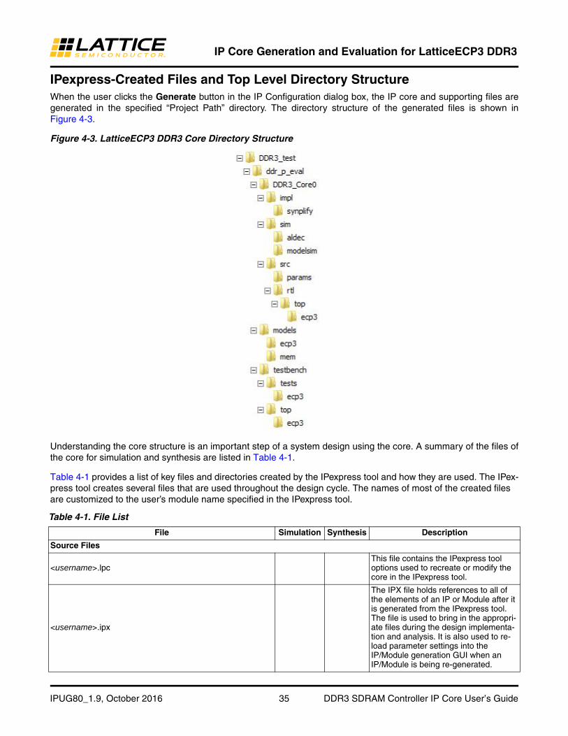
IP Core Generation and Evaluation for LatticeECP3 DDR3
IPUG80_1.9, October 2016 35 DDR3 SDRAM Controller IP Core User’s Guide
IPexpress-Created Files and Top Level Directory StructureWhen the user clicks the Generate button in the IP Configuration dialog box, the IP core and supporting files are generated in the specified “Project Path” directory. The directory structure of the generated files is shown in Figure 4-3.
Figure 4-3. LatticeECP3 DDR3 Core Directory Structure
Understanding the core structure is an important step of a system design using the core. A summary of the files of the core for simulation and synthesis are listed in Table 4-1.
Table 4-1 provides a list of key files and directories created by the IPexpress tool and how they are used. The IPex-press tool creates several files that are used throughout the design cycle. The names of most of the created files are customized to the user’s module name specified in the IPexpress tool.
Table 4-1. File List
File Simulation Synthesis Description
Source Files
<username>.lpcThis file contains the IPexpress tool options used to recreate or modify the core in the IPexpress tool.
<username>.ipx
The IPX file holds references to all of the elements of an IP or Module after it is generated from the IPexpress tool. The file is used to bring in the appropri-ate files during the design implementa-tion and analysis. It is also used to re-load parameter settings into the IP/Module generation GUI when an IP/Module is being re-generated.

IP Core Generation and Evaluation for LatticeECP3 DDR3
IPUG80_1.9, October 2016 36 DDR3 SDRAM Controller IP Core User’s Guide
..\params\ddr3_sdram_mem_params.v Yes This file provides user options of the IP for the simulation models.
<username>_beh.v Yes This is the obfuscated core simulation model.
..\top\ecp3\ddr3_sdram_mem_top_wrapper.v
..\top\ecp3\ddr3_sdram_mem_top_wrapper.vhd
Yes
This is the top level file for simulation and synthesis (.v file if Verilog is selected or .vhd file if VHDL is selected). This file has black-box instan-tiations of the core and I/O modules and also source instantiation of clock syn-chronization module. Refer the section DUMMY LOGIC removal for more details.
<username>.ngo YesThis file provides the synthesized IP core.
Model Files
..\models\ecp3\ddr3_clks.v YesThese are source files of clock synchro-nization logic. PLL and DQSDLL are used to generate system clock (SCLK) for the core, edge clocks (ECLK and SCLK2x) for I/O logic.
..\models\ecp3\ddr3_pll.v Yes
..\models\ecp3\jitter_filter.v Yes
..\models\ecp3\clk_stop.v Yes
..\models\ecp3\clk_phase.v Yes
..\models\ecp3\pll_controls.v Yes
..\models\mem\ddr3.v Yes DIMM simulation model. (DIMM_Type : dimm for UDIMM, rdimm for RDIMM), (mem_data_width: 8/16/24/32/40/48/56/64/72).
..\models\mem\ddr3_<DIMM_type>_<mem_data_width>.v Yes
..\models\mem\ddr3_parameters.vh Yes
Evaluation Testbench Files
..\testbench\top\ecp3\test_mem_ctrl.v YesThis is the evaluation testbench top level file.
..\testbench\top\ecp3\Monitor.v
..\testbench\top\ecp3\odt_watchdog.vYes
These are monitor files for the evalua-tion test bench.
..\tests\ecp3\cmd_gen.v YesThis is the command generator for the evaluation test bench.
..\tests\ecp3\tb_config_params.v YesThis file is the test bench configuration parameter.
..\tests\ecp3\testcase.v Yes This file is the evaluation test bench.
Evaluation Simulation Script Files
..\sim\aldec\<core_name>_eval.do Yes This file is the Active-HDL script.
..\sim\aldec\<core_name>_gatesim_<synthesis>.do
Yes
This file is the Active-HDL script for netlist simulation. This file is generated only if the selected device package has enough I/Os for all the user side and memory side signals. <synthesis>: Precision or Synplify
..\sim\modelsim\<core_name>_eval.do Yes This file is the ModelSim script.
Table 4-1. File List (Continued)
File Simulation Synthesis Description

IP Core Generation and Evaluation for LatticeECP3 DDR3
IPUG80_1.9, October 2016 37 DDR3 SDRAM Controller IP Core User’s Guide
DDR3 Memory Controller IP File StructureThe DDR3 memory controller IP consists of the following four major functional blocks:
• Top-level wrapper (RTL)
• Obfuscated memory controller top-level wrapper for simulation and encrypted netlist memory controller core for synthesis
• Clock Synchronous Module (RTL for simulation and Verilog flow synthesis or netlist for VHDL flow synthesis)
All of these blocks are required to implement the IP on the target FPGA device. Figure 4-4 depicts the interconnec-tion among those blocks.
Figure 4-4. File Structure of DDR3 Memory Controller IP
..\sim\modelsim\<core_name>_gatesim_<synthesis>.do
Yes
This file is the ModelSim script for netlist simulation. This file is generated only if the selected device package has enough I/Os for all the user side and memory side signals. <synthesis>: Precision or Synplify
Evaluation Implementation Script Files
..\impl\synplify\<username>_eval.ldf Yes
This is the Diamond project file for Syn-plify flow
..\impl\synplify\<username>_eval.lpf Yes
This is the par preference file for Syn-plify flow
..\impl\synplify\post_route_trace.prf Yes
This is the post_route preference file for Synplify flow
Table 4-1. File List (Continued)
File Simulation Synthesis Description
Top-Level Wrapper (RTL)
Parameter File
DDR3 MC
Clock Synchronous Module (CSM)
Local User Logic
System Clock
DDR MemoryDDR3 PHY
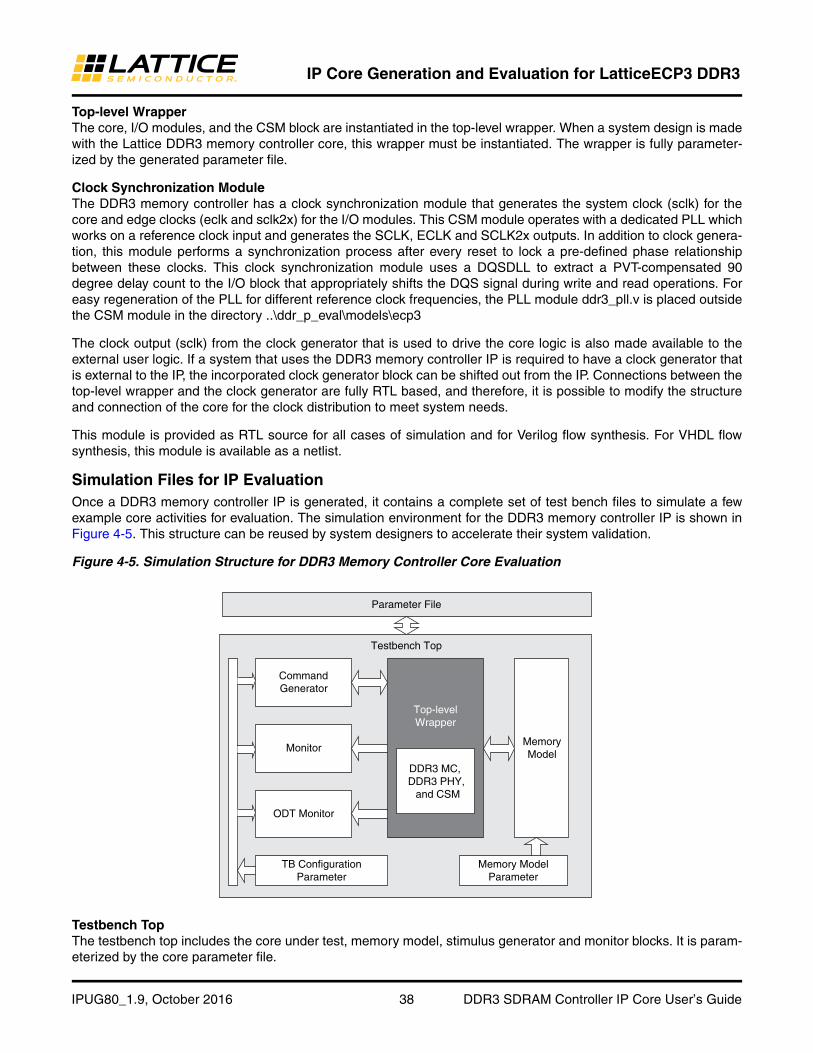
IP Core Generation and Evaluation for LatticeECP3 DDR3
IPUG80_1.9, October 2016 38 DDR3 SDRAM Controller IP Core User’s Guide
Top-level WrapperThe core, I/O modules, and the CSM block are instantiated in the top-level wrapper. When a system design is made with the Lattice DDR3 memory controller core, this wrapper must be instantiated. The wrapper is fully parameter-ized by the generated parameter file.
Clock Synchronization ModuleThe DDR3 memory controller has a clock synchronization module that generates the system clock (sclk) for the core and edge clocks (eclk and sclk2x) for the I/O modules. This CSM module operates with a dedicated PLL which works on a reference clock input and generates the SCLK, ECLK and SCLK2x outputs. In addition to clock genera-tion, this module performs a synchronization process after every reset to lock a pre-defined phase relationship between these clocks. This clock synchronization module uses a DQSDLL to extract a PVT-compensated 90 degree delay count to the I/O block that appropriately shifts the DQS signal during write and read operations. For easy regeneration of the PLL for different reference clock frequencies, the PLL module ddr3_pll.v is placed outside the CSM module in the directory ..\ddr_p_eval\models\ecp3
The clock output (sclk) from the clock generator that is used to drive the core logic is also made available to the external user logic. If a system that uses the DDR3 memory controller IP is required to have a clock generator that is external to the IP, the incorporated clock generator block can be shifted out from the IP. Connections between the top-level wrapper and the clock generator are fully RTL based, and therefore, it is possible to modify the structure and connection of the core for the clock distribution to meet system needs.
This module is provided as RTL source for all cases of simulation and for Verilog flow synthesis. For VHDL flow synthesis, this module is available as a netlist.
Simulation Files for IP EvaluationOnce a DDR3 memory controller IP is generated, it contains a complete set of test bench files to simulate a few example core activities for evaluation. The simulation environment for the DDR3 memory controller IP is shown in Figure 4-5. This structure can be reused by system designers to accelerate their system validation.
Figure 4-5. Simulation Structure for DDR3 Memory Controller Core Evaluation
Testbench TopThe testbench top includes the core under test, memory model, stimulus generator and monitor blocks. It is param-eterized by the core parameter file.
Testbench Top
Parameter File
CommandGenerator
MemoryModel
Monitor
ODT Monitor
Top-levelWrapper
TB ConfigurationParameter
Memory ModelParameter
DDR3 MC, DDR3 PHY, and CSM

IP Core Generation and Evaluation for LatticeECP3 DDR3
IPUG80_1.9, October 2016 39 DDR3 SDRAM Controller IP Core User’s Guide
Obfuscated Controller Simulation ModelThe obfuscated top level wrapper simulation model for the controller includes the MC and PHY modules. This obfuscated simulation model must be included in the simulation.
Command GeneratorThe command generator generates stimuli for the core. The core initialization and command generation activities are predefined in the provided test case module. It is possible to customize the test case module to see the desired activities of the core.
MonitorThe monitor block monitors both the local user interface and DDR3 interface activities and generates a warning or an error if any violation is detected. It also validates the core data transfer activities by comparing the read data with the written data.
Testbench Configuration ParameterThe testbench configuration parameter provides the parameters for testbench files. These parameters are derived from the core parameter file and are not required to configure them separately. For those users who need a special memory configuration, however, modifying this parameter set might provide a support for the desired configuration.
Memory ModelThe DDR3 memory controller testbench uses a memory simulation model provided by one of the most popular memory vendors. If a different memory model is required, it can be used by simply replacing the instantiation of the model from the memory configuration modules located in the same folder.
Memory Model ParameterThis memory parameter file comes with the memory simulation model. It contains the parameters that the memory simulation model needs. It is not necessary for users to change any of these parameters.
Evaluation Script FileA ModelSim and Aldec ACTIVE-HDL simulation macro script files are included for instant evaluation of the IP. All required files for simulation are included in the macro script. This simulation script can be used as a starting point of a user simulation project.
Note on Shortening Simulation Run TimeThe memory controller implements many timers to comply with JEDEC specifications. Due to these timers the functional simulation takes longer time at various stages of the simulation. In order to reduce the simulation run time, the controller has an option to lower the timer counts, particularly on those timers for waiting period. This option can be enabled by adding a define SIM in the simulation script. It is important to note that this reduced timer value is good only for the simulation and this define should not be included in the synthesis script.
Hardware EvaluationThe DDR3 SDRAM IP core supports Lattice’s IP hardware evaluation capability, which makes it possible to create versions of the IP core that operate in hardware for a limited period of time (approximately four hours) without requiring the purchase of an IP license. It may also be used to evaluate the core in hardware in user-defined designs.
Enabling Hardware Evaluation in DiamondChoose Project > Active Strategy > Translate Design Settings. The hardware evaluation capability may be enabled/disabled in the Strategy dialog box. It is enabled by default.

IP Core Generation and Evaluation for LatticeECP3 DDR3
IPUG80_1.9, October 2016 40 DDR3 SDRAM Controller IP Core User’s Guide
Updating/Regenerating the IP CoreBy regenerating an IP core with the IPexpress tool, you can modify any of its settings including: device type, design entry method, and any of the options specific to the IP core. Regenerating can be done to modify an existing IP core or to create a new but similar one.
To regenerate an IP core in Diamond:
1. In IPexpress, click the Regenerate button.
2. In the Regenerate view of IPexpress, choose the IPX source file of the module or IP you wish to regenerate.
3. IPexpress shows the current settings for the module or IP in the Source box. Make your new settings in the Tar-get box.
4. If you want to generate a new set of files in a new location, set the new location in the IPX Target File box. The base of the file name will be the base of all the new file names. The IPX Target File must end with an .ipx exten-sion.
5. Click Regenerate. The module’s dialog box opens showing the current option settings.
6. In the dialog box, choose the desired options. To get information about the options, click Help. Also, check the About tab in IPexpress for links to technical notes and user guides. IP may come with additional information. As the options change, the schematic diagram of the module changes to show the I/O and the device resources the module will need.
7. To import the module into your project, if it’s not already there, select Import IPX to Diamond Project (not available in stand-alone mode).
8. Click Generate.
9. Check the Generate Log tab to check for warnings and error messages.
10.Click Close.
The IPexpress package file (.ipx) supported by Diamond holds references to all of the elements of the generated IP core required to support simulation, synthesis and implementation. The IP core may be included in a user's design by importing the .ipx file to the associated Diamond project. To change the option settings of a module or IP that is already in a design project, double-click the module’s .ipx file in the File List view. This opens IPexpress and the module’s dialog box showing the current option settings. Then go to step 6 above.

IPUG80_1.9, October 2016 41 DDR3 SDRAM Controller IP Core User’s Guide
This chapter provides information on how to generate the DDR3 SDRAM Controller IP core using the Lattice Dia-mond design software IPexpress tool, and how to include the core in a top-level design.
The DDR3 SDRAM Controller IP core can be used in the ECP5 device family.
For example information and known issues on this core see the Lattice DDR3 IP ReadMe document. This file is available once the core is installed in Diamond. The document provides information on creating an evaluation ver-sion of the core for use in Diamond and simulation
Getting StartedThe DDR3 SDRAM IP core is available for download from the Lattice IP Server using the Clarity Designer tool. The IP files are automatically installed using ispUPDATE technology in any customer-specified directory. After the IP core has been installed, the IP core becomes available in the Clarity Designer tool dialog box shown in Figure 5-1.
• Create new Clarity design - Choose to create a new Clarity Design project directory in which the DDR3 SDRAM IP core will be generated.
• Design Location - Clarity Design project directory Path.
• Design Name - Clarity Design project name.
• HDL Output - Hardware Description Language Output Format (Verilog or VHDL).
• Open Clarity design - Open an existing Clarity Design project.
• Design File - Name of existing Clarity Design project file with .sbx extension.
Figure 5-1. Clarity Designer Tool Dialog Box
Chapter 5:
IP Core Generation and Evaluation for ECP5 DDR3

IP Core Generation and Evaluation for ECP5 DDR3
IPUG80_1.9, October 2016 42 DDR3 SDRAM Controller IP Core User’s Guide
The Clarity Designer IP catalog is shown in Figure 5-2. You can generate DDR3 SDRAM IP core configuration by double-clicking the IP name in the Catalog tab.
Figure 5-2. Clarity Designer IP Catalog Window
In the DDR3 SDRAM Controller dialog box shown Figure 5-3, specify the following:
• Instance Name - The instance module name of the DDR3 SDRAM IP core.
Figure 5-3. IP Generation Dialog Box
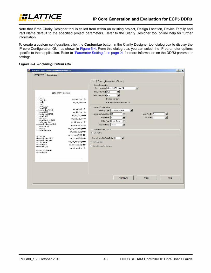
IP Core Generation and Evaluation for ECP5 DDR3
IPUG80_1.9, October 2016 43 DDR3 SDRAM Controller IP Core User’s Guide
Note that if the Clarity Designer tool is called from within an existing project, Design Location, Device Family and Part Name default to the specified project parameters. Refer to the Clarity Designer tool online help for further information.
To create a custom configuration, click the Customize button in the Clarity Designer tool dialog box to display the IP core Configuration GUI, as shown in Figure 5-4. From this dialog box, you can select the IP parameter options specific to their application. Refer to “Parameter Settings” on page 21 for more information on the DDR3 parameter settings.
Figure 5-4. IP Configuration GUI
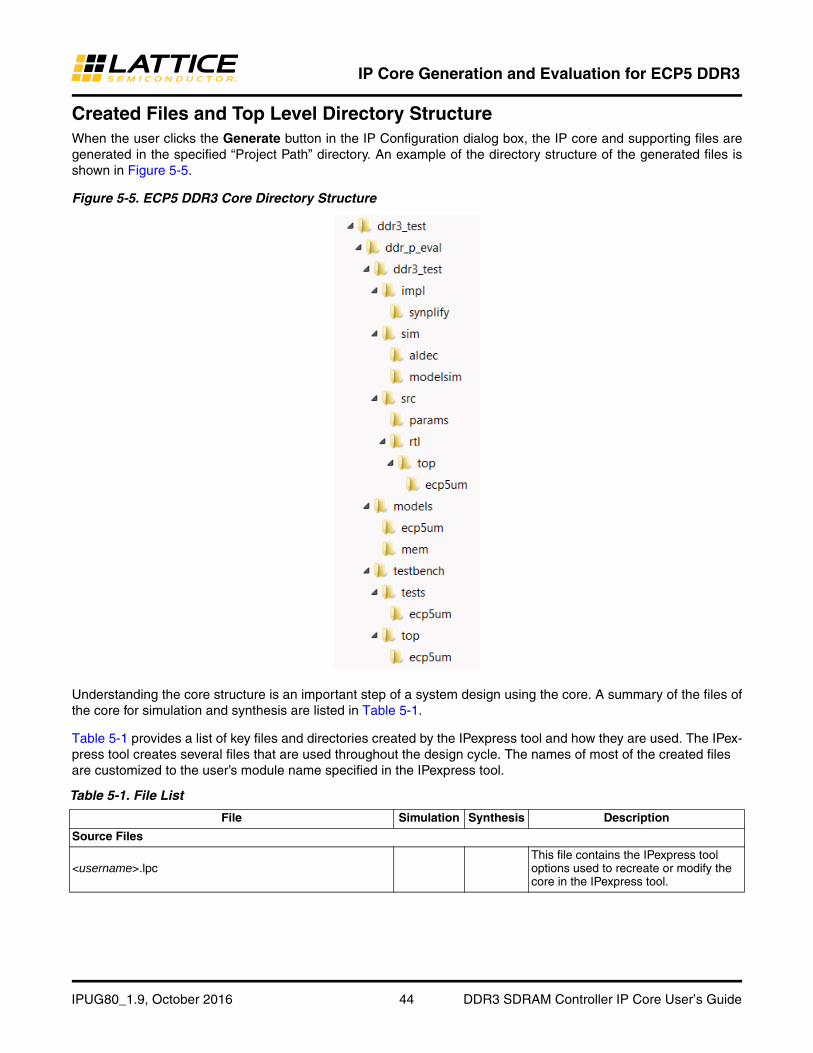
IP Core Generation and Evaluation for ECP5 DDR3
IPUG80_1.9, October 2016 44 DDR3 SDRAM Controller IP Core User’s Guide
Created Files and Top Level Directory StructureWhen the user clicks the Generate button in the IP Configuration dialog box, the IP core and supporting files are generated in the specified “Project Path” directory. An example of the directory structure of the generated files is shown in Figure 5-5.
Figure 5-5. ECP5 DDR3 Core Directory Structure
Understanding the core structure is an important step of a system design using the core. A summary of the files of the core for simulation and synthesis are listed in Table 5-1.
Table 5-1 provides a list of key files and directories created by the IPexpress tool and how they are used. The IPex-press tool creates several files that are used throughout the design cycle. The names of most of the created files are customized to the user’s module name specified in the IPexpress tool.
Table 5-1. File List
File Simulation Synthesis Description
Source Files
<username>.lpcThis file contains the IPexpress tool options used to recreate or modify the core in the IPexpress tool.

IP Core Generation and Evaluation for ECP5 DDR3
IPUG80_1.9, October 2016 45 DDR3 SDRAM Controller IP Core User’s Guide
<username>.ipx
The IPX file holds references to all of the elements of an IP or Module after it is generated from the IPexpress tool (Diamond version only). The file is used to bring in the appropriate files during the design implementation and analy-sis. It is also used to re-load parameter settings into the IP/Module generation GUI when an IP/Module is being re-generated.
..\params\ddr3_sdram_mem_params.v Yes This file provides user options of the IP for the simulation models
<username>_beh.v Yes This is the obfuscated core simulation model.
..\rtl\top\<device>\ddr3_sdram_mem_top_wrapper.v
..\rtl\top\<device>\ddr3_sdram_mem_top_wrapper.vhd
Yes
This is the top Level file for simulation and synthesis (.v file if Verilog is selected or .vhd file if VHDL is selected). This file has black-box instan-tiations of the core and I/O modules and also source instantiation of clock syn-chronization module. Refer the section DUMMY LOGIC removal for more details.
<username>.ngo YesThis file provides the synthesized IP core.
Model Files
..\models\<device>\ddr3_clks.v Yes These are source files of Clock syn-chronization logic. PLL and DQSDLL are used to generate system clock (SCLK) for the core and edge clock (ECLK) for I/O logic.
..\models\<device>\ddr3_pll.vYes
..\models\mem\ddr3.v Yes DIMM simulation model. (DIMM_Type : dimm for UDIMM, rdimm for RDIMM), (mem_data_width: 8/16/24/32/40/48/56/64/72).
..\models\mem\ddr3_<DIMM_type>_<mem_data_width>.v Yes
..\models\mem\ddr3_parameters.vh Yes
Evaluation Test Bench Files
..\testbench\top\<device>\test_mem_ctrl.v YesThis is the evaluation test bench top level file.
..\testbench\top\<device>\Monitor.v
..\testbench\top\<device>\odt_watchdog.vYes
These are monitor files for the evalua-tion test bench.
..\tests\<device>\cmd_gen.v YesThis is the command generator for the evaluation test bench.
..\tests\<device>\tb_config_params.v YesThis file is the test bench configuration parameter.
..\tests\<device>\testcase.v Yes This file is the evaluation test bench.
Evaluation Simulation Script Files
..\sim\aldec\<core_name>_eval.do Yes This file is the Aldec script.
..\sim\aldec\<core_name>_gatesim_<synthesis>.do
Yes
This file is the Aldec script for netlist simulation. This file is generated only if the selected device package has enough I/Os for all the user side and memory side signals. <synthesis> : precision or synplify
Table 5-1. File List (Continued)
File Simulation Synthesis Description
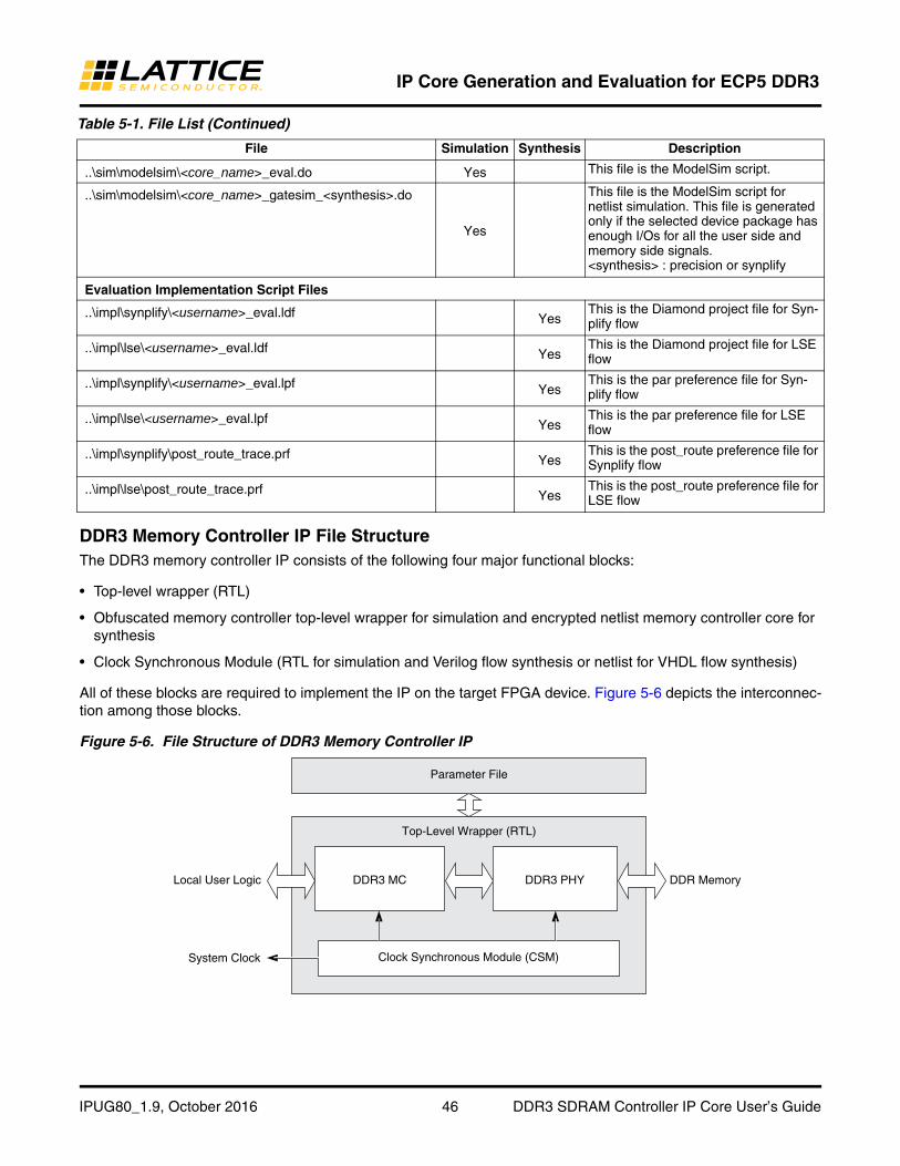
IP Core Generation and Evaluation for ECP5 DDR3
IPUG80_1.9, October 2016 46 DDR3 SDRAM Controller IP Core User’s Guide
DDR3 Memory Controller IP File StructureThe DDR3 memory controller IP consists of the following four major functional blocks:
• Top-level wrapper (RTL)
• Obfuscated memory controller top-level wrapper for simulation and encrypted netlist memory controller core for synthesis
• Clock Synchronous Module (RTL for simulation and Verilog flow synthesis or netlist for VHDL flow synthesis)
All of these blocks are required to implement the IP on the target FPGA device. Figure 5-6 depicts the interconnec-tion among those blocks.
Figure 5-6. File Structure of DDR3 Memory Controller IP
..\sim\modelsim\<core_name>_eval.do Yes This file is the ModelSim script.
..\sim\modelsim\<core_name>_gatesim_<synthesis>.do
Yes
This file is the ModelSim script for netlist simulation. This file is generated only if the selected device package has enough I/Os for all the user side and memory side signals. <synthesis> : precision or synplify
Evaluation Implementation Script Files
..\impl\synplify\<username>_eval.ldf Yes
This is the Diamond project file for Syn-plify flow
..\impl\lse\<username>_eval.ldf Yes
This is the Diamond project file for LSE flow
..\impl\synplify\<username>_eval.lpf Yes
This is the par preference file for Syn-plify flow
..\impl\lse\<username>_eval.lpf Yes
This is the par preference file for LSE flow
..\impl\synplify\post_route_trace.prf Yes
This is the post_route preference file for Synplify flow
..\impl\lse\post_route_trace.prf Yes
This is the post_route preference file for LSE flow
Table 5-1. File List (Continued)
File Simulation Synthesis Description
Top-Level Wrapper (RTL)
Parameter File
DDR3 MC
Clock Synchronous Module (CSM)
Local User Logic
System Clock
DDR MemoryDDR3 PHY
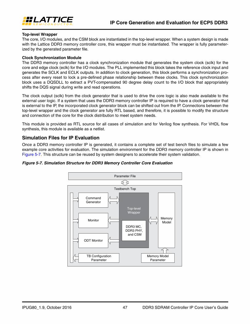
IP Core Generation and Evaluation for ECP5 DDR3
IPUG80_1.9, October 2016 47 DDR3 SDRAM Controller IP Core User’s Guide
Top-level WrapperThe core, I/O modules, and the CSM block are instantiated in the top-level wrapper. When a system design is made with the Lattice DDR3 memory controller core, this wrapper must be instantiated. The wrapper is fully parameter-ized by the generated parameter file.
Clock Synchronization ModuleThe DDR3 memory controller has a clock synchronization module that generates the system clock (sclk) for the core and edge clock (eclk) for the I/O modules. The PLL implemented this block takes the reference clock input and generates the SCLK and ECLK outputs. In addition to clock generation, this block performs a synchronization pro-cess after every reset to lock a pre-defined phase relationship between these clocks. This clock synchronization block uses a DQSDLL to extract a PVT-compensated 90 degree delay count to the I/O block that appropriately shifts the DQS signal during write and read operations.
The clock output (sclk) from the clock generator that is used to drive the core logic is also made available to the external user logic. If a system that uses the DDR3 memory controller IP is required to have a clock generator that is external to the IP, the incorporated clock generator block can be shifted out from the IP. Connections between the top-level wrapper and the clock generator are fully RTL based, and therefore, it is possible to modify the structure and connection of the core for the clock distribution to meet system needs.
This module is provided as RTL source for all cases of simulation and for Verilog flow synthesis. For VHDL flow synthesis, this module is available as a netlist.
Simulation Files for IP EvaluationOnce a DDR3 memory controller IP is generated, it contains a complete set of test bench files to simulate a few example core activities for evaluation. The simulation environment for the DDR3 memory controller IP is shown in Figure 5-7. This structure can be reused by system designers to accelerate their system validation.
Figure 5-7. Simulation Structure for DDR3 Memory Controller Core Evaluation
Testbench Top
Parameter File
CommandGenerator
MemoryModel
Monitor
ODT Monitor
Top-levelWrapper
TB ConfigurationParameter
Memory ModelParameter
DDR3 MC, DDR3 PHY, and CSM

IP Core Generation and Evaluation for ECP5 DDR3
IPUG80_1.9, October 2016 48 DDR3 SDRAM Controller IP Core User’s Guide
Test Bench TopThe test bench top includes the core under test, memory model, stimulus generator and monitor blocks. It is parameterized by the core parameter file.
Obfuscated Controller Simulation ModelThe obfuscated top level wrapper simulation model for the controller includes the MC and PHY modules. This obfuscated simulation model must be included in the simulation.
Command GeneratorThe command generator generates stimuli for the core. The core initialization and command generation activities are predefined in the provided test case module. It is possible to customize the test case module to see the desired activities of the core.
MonitorThe monitor block monitors both the local user interface and DDR3 interface activities and generates a warning or an error if any violation is detected. It also validates the core data transfer activities by comparing the read data with the written data.
Test Bench Configuration ParameterThe test bench configuration parameter provides the parameters for test bench files. These parameters are derived from the core parameter file and are not required to configure them separately. For those users who need a special memory configuration, however, modifying this parameter set might provide a support for the desired configuration.
Memory ModelThe DDR3 memory controller test bench uses a memory simulation model provided by one of the most popular memory vendors. If a different memory model is required, it can be used by simply replacing the instantiation of the model from the memory configuration modules located in the same folder.
Memory Model ParameterThis memory parameter file comes with the memory simulation model. It contains the parameters that the memory simulation model needs. It is not necessary for users to change any of these parameters.
Evaluation Script FileA ModelSim and Aldec ACTIVE-HDL simulation macro script files are included for instant evaluation of the IP. All required files for simulation are included in the macro script. This simulation script can be used as a starting point of a user simulation project.
Note on Shortening Simulation Run TimeThe memory controller implements many timers to comply with JEDEC specifications. Due to these timers the functional simulation takes longer time at various stages of the simulation. In order to reduce the simulation run time, the controller has an option to lower the timer counts, particularly on those timers for waiting period. This option can be enabled by adding a define SIM in the simulation script. It is important to note that this reduced timer value is good only for the simulation and this define should not be included in the synthesis script.

IP Core Generation and Evaluation for ECP5 DDR3
IPUG80_1.9, October 2016 49 DDR3 SDRAM Controller IP Core User’s Guide
Hardware EvaluationThe DDR3 SDRAM IP core supports Lattice’s IP hardware evaluation capability, which makes it possible to create versions of the IP core that operate in hardware for a limited period of time (approximately four hours) without requiring the purchase of an IP license. It may also be used to evaluate the core in hardware in user-defined designs.
Enabling Hardware Evaluation in Diamond:Choose Project > Active Strategy > Translate Design Settings. The hardware evaluation capability may be enabled/disabled in the Strategy dialog box. It is enabled by default.
Regenerating/Recreating the IP CoreBy regenerating an IP core with the Clarity Designer tool, you can modify any of the options specific to an existing IP instance. By recreating an IP core with Clarity Designer tool, you can create (and modify if needed) a new IP instance with an existing LPC/IPX configuration file.
Regenerating an IP Core in Clarity Designer ToolTo regenerate an IP core in Clarity Designer:
1. In the Clarity Designer Builder window, right-click on the existing IP instance and choose Config.
2. In the dialog box, choose the desired options. For more information about the options, click Help. You may also click the About tab in the Clarity Designer win-dow for links to technical notes and user guides. The IP may come with additional information. As the options change, the schematic diagram of the module changes to show the I/O and the device resources the module will need.
3. Click Configure.
Recreating an IP Core in Clarity Designer ToolTo recreate an IP core in Clarity Designer:
1. In the Clarity Designer Catalog window, click the Import IP tab at the bottom.
2. In the Import IP tab, choose the existing IPX/LPC source file of the module or IP to regenerate.
3. Specify the instance name in Target Instance. Note that this instance name should not be the same as any of the existing IP instances in the current Clarity Design project.
4. Click Import. The module's dialog box opens showing the option settings.
5. In the dialog box, choose the desired options. For more information about the options, click Help. You may also click the About tab in the Clarity Designer win-dow for links to technical notes and user guides. The IP may come with additional information. As the options change, the schematic diagram of the module changes to show the I/O and the device resources the module will need.
6. Click Configure.

IPUG80_1.9, October 2016 50 DDR3 SDRAM Controller IP Core User’s Guide
This chapter provides supporting information on using the DDR3 SDRAM Controller IP in complete designs.
Understanding PreferencesThe generated preference file has many preferences that will fall mainly into one these categories:
FREQUENCY PreferencesEach clock domain in the controller is defined by a Frequency preference.
MAXDELAY NETThe MAXDELAY NET preference ensures that the net has a minimal net delay and falls within the allowed limit. Since this preference is highly over-constrained, the post-route trace preference file should be used to validate the timing results.
MULTICYCLE / BLOCK PATHThe MULTICYCLE preference is applied to a path that is covered by the FREQUENCY constraint, but is allowed to be relaxed from its FRQUENCY constraint. The FREQUENCY constraint is relaxed in multiples of the clock period.
The BLOCK preference is applied to a path that is not relevant for the timing analysis.
IOBUFThe IOBUF preference assigns the required I/O types and attributes to the DDR3 I/O pads.
LOCATEOnly the em_ddr_dqs pads and the DLL site are located in the provided preference file per user selection. Note that not all I/O pads can be associated with a DQS (em_ddr_dqs) pad in a bank. Since there is a strict DQ-to-DQS association rule in each Lattice FPGA device, it is strongly recommended the DQ-to-DQS associations of the selected pinouts be validated using the implementation software before the PCB routing task is started. The DQ-to-DQS pad associations for a target FPGA device can be found in the datasheet or pinout table of the target device.
For more details on DDR3 pinout guidelines, refer to:
• TN1265, ECP5 High-Speed I/O Interface
• TN1180, LatticeECP3 High-Speed I/O Interface
Handling DDR3 IP Preferences in User Designs• The generated preference file uses the hierarchical paths for nets and cells. These paths are good for the Evalu-
ation environment provided by the IP package. When the DDR3 controller is integrated into the user design, all the hierarchical paths in the preference file should be updated as per the User’s integrated environment. In most cases appending a wild case designation (such as "*/") in the beginning of the path name may be enough.
• The hierarchy structure and name of an internal net used in a preference is subject to change when there are changes in the design or when a different version of a synthesis tool is used. It is the user’s responsibility to track these changes and update them in the preference file. The updated net and path names can be found in the map report file (.mrp) or through Floorplan View and Physical View in Diamond or the Design Planner tool.
• If a preference has a wrong path or wrong name it is dropped by the Place and Route tool and the dropped pref-erences are listed in the static timing report (.twr file). It is very important to check for such dropped preferences in the static timing report.
Chapter 6:
Application Support

Application Support
IPUG80_1.9, October 2016 51 DDR3 SDRAM Controller IP Core User’s Guide
Reset HandlingThe controller provides two reset input ports at the local side. The rst_n signal by default resets both the controller and the memory device. Usually this rst_n is expected to include power_on_reset as well as the system reset and is implemented through global reset net (GSR) by default. Another reset input signal mem_rst_n is available to reset only the memory device, not the controller. In addition to routing this reset to the memory, the controller ensures that the memory reset signal em_ddr_reset_n is asserted at least for a 100 ns period as required by the JEDEC specification, even if the input reset signal mem_rst_n is asserted for less than 100 ns. The minimum required reset assertion time for mem_rst_n is one system clock.
The controller, through the GUI option “Controller Reset to Memory” (see “Controller Reset to Memory” on page 25) allows the user to disable the rst_n or mem_rst_n inputs from resetting the memory. When this option is disabled (unchecked) the memory side output port em_ddr_reset_n is removed from the controller's output ports. In this disabled mode, rst_n resets only the controller. It is the user's responsibility to implement a memory reset logic outside the controller and add a port for the memory reset. In addition, the user memory reset signal gener-ated outside the controller must be fed to the mem_rst_n input of the controller to let the controller know the mem-ory reset assertion. This will enable the IP core to set the memory interface signals at the appropriate state as specified for the reset time.
There may be many applications which need to handle the memory reset outside the IP core. For example, dis-abling the memory reset from the core can be useful when multiple host controllers need to be connected to and share a DDR3 memory.
Dummy Logic RemovalWhen a DDR3 IP core is generated, IPexpress assigns all the signals from both the DDR3 and local user interfaces to the I/O pads. The number of DDR3 IP’s user interface signals for read and write data buses together is normally more than eight times than that of the DDR3 memory interface. It is impossible for the core to be generated if the selected device does not have enough I/O pad resources. To facilitate the core evaluation with smaller package devices, IPexpress inserts dummy logic to decrease the I/O pad counts by reducing the local read_data and write_data bus sizes. With the dummy logic, a core can be successfully generated and evaluated even with smaller pad counts. The PAR process can be completed without a resource violation so that one can evaluate the perfor-mance and utilization of the core. However, the synthesized netlist will not function correctly because of the inserted dummy logic.The core with dummy logic, therefore, must be used only for evaluation.
Top-level Wrapper File Only for Evaluation Implementation For eval implementation using the Verilog core, a separate top level wrapper file, ddr3_sdram_mem_top_wrapper.v is provided in the directory ..\ddr_p_eval\<usr_name>\impl. This wrapper file has a reduced number of local side data busses for the reason mentioned in the previous paragraph. The eval par project file<usr_name>_eval.syn in the directory ..\ddr_p_eval\<usr_name>\impl\synplicity (or ..\ddr_p_eval\<usr_name>\impl\precision) points to this wrapper file for running evaluation imple-mentation.
For the VHDL flow, the top-level wrapper file ..\ddr_p_eval\<usr_name>\impl\ddr3_sdram_mem_top_wrapper.vhd is provided for evaluation implementation.
Note that this top-level wrapper file is not used for evaluation simulation.
Top-level Wrapper file for All Simulation Cases and Implementation in a User’s Design In real applications, since back end user logic design is attached to the core, most of the user side interface signals are embedded within the FPGA fabric and will not be connected to the pads of the FPGA fabric. There is a main top level wrapper file, ddr3_sdram_mem_top_wrapper.v, in the directory ..\ddr_p_eval\<usr_name>\src\rtl\top\ecp5um. This wrapper is generated with a full local side data

Application Support
IPUG80_1.9, October 2016 52 DDR3 SDRAM Controller IP Core User’s Guide
bus and is meant for simulation as well as for the final integration with user’s logic for synthesis. The user’s par proj-ect file should point to this top-level wrapper file while implementing the IP core in the user’s application.
RDIMM Module SupportThe controller is designed to work with the default settings of the RDIMM module's SSTE32882 Registering Clock Driver. There is no controller support to program the control word registers of the Clock Driver.
A Note on Chip Select Signal Handling when a Single Rank RDIMM Module is UsedIn order to set the Clock Driver in normal mode, the controller provides two bits for the chip select signal em_ddr_cs_n and always drives em_ddr_cs_n[1] high. The user is advised to connect both chip select bits to the corresponding chip select input pins of the RDIMM module. Leaving the chip select bit 1 input of the RDIMM mod-ule open will lead to incorrect operation of the RDIMM module.

IPUG80_1.9, October 2016 53 DDR3 SDRAM Controller IP Core User’s Guide
The functionality of the DDR3 SDRAM Controller IP core has been verified via simulation and hardware testing in a variety of environments, including:
• Simulation environment verifying proper DDR3 functionality when testing with Industry standard Denali’s MMAV (Memory Modeler - Advanced Verification) verification IP
• Hardware validation of the IP implemented on Lattice FPGA evaluation boards. Specific testing has included: – Verifying proper DDR3 protocol functionality – Verifying DDR3 electrical compliance.
• In-house interoperability testing with multiple DIMM modules
Chapter 7:
Core Validation

IPUG80_1.9, October 2016 54 DDR3 SDRAM Controller IP Core User’s Guide
This chapter contains information about Lattice Technical Support, additional references, and document revision history.
Lattice Technical SupportSubmit a technical support case via www.latticesemi.com/techsupport.
References• TN1265, ECP5 High-Speed I/O Interface
• TN1180, LatticeECP3 High-Speed I/O Interface
Revision History
DateDocument
VersionIP Core Version Change Summary
October 2016 1.9 3.1 Updated Write Leveling description in the Initialization Module section.
Added support for ECP5-5G (LFE5UM5G) devices.
Updated Type Tab section. Added reference to the Initialization Module section in the description of write leveling.
Updated Table 3-1, IP Core Parameters. Revised Memory Data Bus size Range/Options.
Updated Table 5-1, File List. Revised Model Files mem_data_width.
Updated Lattice Technical Support section.
September 2014 1.8 3.0 Combined user's guide version for both LatticeECP3 DDR3 IP and ECP5 DDR3 IP.
May 2014 1.7 3.0esr User's guide version with information only on ECP5 DDR3 IP.
Streamlined the preference file for easy implementation.
Write level error signal wl_err is added as a local side I/O port.
December 2013 01.6 01.5 Updated DDR3 SDRAM Controller Block Diagram figure.
Added notes to Memory Device Timing Tab figure and MAXDELAY NET section.
Updated Write leveling description.
Updated Technical Support Assistance information.
March 2012 01.5 1.4 Added support for LatticeECP3-17EA-328 device.
Added support for LatticeECP3 device speed grades: -6L, -7L, -8L and -9.
Updated Signal Descriptions table – Updated description for wl_rst_datapath.
Updated IP Core Parameters table.
Updated 2T Mode text section.
Replaced figure: DDR3 SDRAM IP Core Pin Selection Options in the IPexpress Tool.
Replaced figure: IPexpress Tool Dialog Box
Replaced figure: Configuration GUI
Updated Clock Synchronization text section.
Core Validation section – Added note on netlist simulation.
Removed references to ispLEVER design software.
December 2011 01.4 1.3 Updated Appendix B with reference to SSN guidelines for DQS pin placement.
Chapter 8:
Support Resources

Support Resources
IPUG80_1.9, October 2016 55 DDR3 SDRAM Controller IP Core User’s Guide
June 2011 01.3 1.3 Added support for Dual Rank memory.
During an Auto Refresh command burst, the Precharge command is issued only for the first Refresh command.
Resolved cmd_rdy inactive issue during long power down period.
Added restricted netlist simulation capability.
December 2010 01.2 1.2 Added support for RDIMM module.
Added support for x4 memory device configuration.
Improved core throughput.
Added selection for controller reset to memory.
Improved Clock Synchronization Module (CSM).
July 2010 01.1 1.1 Added support for Diamond software.
Added support for all memory datawidths.
Added Support for LatticeECP3-EA devices.
Added Write leveling selection.
February 2010 01.0 1.0 Initial release.
DateDocument
VersionIP Core Version Change Summary

IPUG80_1.9, October 2016 56 DDR3 SDRAM Controller IP Core User’s Guide
This appendix gives resource utilization information for Lattice FPGAs using the DDR3 SDRAM Controller IP core. The IP configurations shown in this chapter were generated using the IPexpress software tool. IPexpress is the Lat-tice IP configuration utility, and is included as a standard feature of the Diamond design tools. Details regarding the usage of IPexpress can be found in the IPexpress and Diamond help systems. For more information on the Dia-mond design tools, visit the Lattice web site at www.latticesemi.com//Products/DesignSoftware.
ECP5 DevicesTable A-1. Performance and Resource Utilization1
Ordering Part NumberThe Ordering Part Number (OPN) for the DDR3 SDRAM Controller IP on ECP5 devices is DDR3-E5-U or DDR3_E5_UT.
Parameters Slices LUTs Registers I/O2 fMAX (MHz)3
Data Bus Width: 8 (x8) 1800 2600 1700 42
400 MHz (800 Mbps)
Data Bus Width: 16 (x8) 1900 2650 1900 53
Data Bus Width: 24 (x8) 2000 2850 2050 64
Data Bus Width: 32 (x8) 2100 2950 2250 75
Data Bus Width: 40 (x8) 2200 3000 2450 86
Data Bus Width: 48 (x8) 2350 3200 2650 97
Data Bus Width: 56 (x8) 2450 3250 2850 108
Data Bus Width: 64 (x8) 2600 3450 3100 119
Data Bus Width: 72 (x8) 2700 3500 3300 130 333 MHz (666 Mbps)
1. Performance and utilization data are generated targeting an LFE5U/LFE5UM-85F-8BG756C device using Lattice Diamond 3.3 design soft-ware with an LFE5U/LFE5UM control pack. Performance may vary when using a different software version or targeting a different device density or speed grade within the ECP5 family.
2. Numbers shown in the I/O column represent the number of primary I/Os at the DDR3 memory interface. User interface (local side) I/Os are not included.
3. The DDR3 IP core can operate at 400 MHz (800 DDR3) in the fastest speed-grade (-8) when the data width is 64 bits or less and one chip select is used.
Appendix A:
Resource Utilization

Resource Utilization
IPUG80_1.9, October 2016 57 DDR3 SDRAM Controller IP Core User’s Guide
LatticeECP3 DevicesTable A-2. Performance and Resource Utilization1, 2
Ordering Part NumberThe Ordering Part Number (OPN) for the DDR3 SDRAM Controller IP on LatticeECP3-EA devices is DDR3-E3-U1.
Parameters Slices LUTs Registers I/O fMAX (MHz)3
Data Bus Width: 8 (x8) 1741 2519 1764 42
400 MHz (800 Mbps)
Data Bus Width: 16 (x8) 1947 2661 2129 53
Data Bus Width: 24 (x8) 2157 2820 2467 64
Data Bus Width: 32 (x8) 2337 2934 2803 75
Data Bus Width: 40 (x8) 2266 2890 2685 86
Data Bus Width: 48 (x8) 2401 2968 2886 97
Data Bus Width: 56 (x8) 2532 3080 3112 108
Data Bus Width: 64 (x8) 2662 3212 3320 119
Data Bus Width: 72 (x8) 2795 3348 3469 130 333 MHz (666 Mbps)
1. Performance and utilization data are generated targeting an LFE3-150EA-8FN1156C device using Lattice Diamond 3.3 software. Perfor-mance may vary when using a different software version or targeting a different device density or speed grade within the LatticeECP3 fam-ily.
2. LatticeECP3 ‘EA’ silicon support only.3. The DDR3 IP core can operate at 400 MHz (800 DDR3) in the fastest speed-grade (-8, -8L or -9) when the data width is 64 bits or less and
one chip select is used.

IPUG80_1.9, October 2016 58 DDR3 SDRAM Controller IP Core User’s Guide
The maximum DDR3 bus datawidth supported in a LatticeECP3 device depends on the number of DQS groups available in the device. The available number of DQS groups in the left or right side varies with each LatticeECP3 and ECP5 device density and package.
While all the DQS groups fully support DDR3 electrical and protocol specifications, the user is recommended to consider Simultaneous Switching Noise (SSN) guidelines for the proper placement of the DQS pins.
These guidelines are driven by the following factors:
• Properly terminated interface
• SSN optimized PCB layout
• SSN considered I/O pad assignment
• Use of pseudo power pads
Technical note TN1180, LatticeECP3 High-Speed I/O Interface provides detailed information on the SSN-consid-ered I/O pad assignment and the use of pseudo power pads. This technical note also inclues a Recommended DQS Group Allocation table for each LatticeECP3 device and package. These tables can be used as a baseline. The user is advised to derive the best DQS placement for higher or lower data widths depending on the level of adherence to all the factors of the Simultaneous Switching Noise (SSN) guidelines.
Appendix B:
Lattice Device Versus DDR3 IP Matrix

IPUG80_1.9, October 2016 59 DDR3 SDRAM Controller IP Core User’s Guide
LatticeECP3 DDR3 IP has a few critical macro like blocks that require specific placement locations. This is achieved by adding a number of “LOCATE” constraints in the preference file for these blocks.There are two groups of locate constraints applied in the preference file.
• One group consists of a list of locate constraints for the read_pulse_delay logic. Each of these locate constraints corresponds to a particular DQS pin.
• One group consists of a list of locate constraints for the clock synchronization logic. Each clk_in pin has one group of these locate preferences.
As per the DQS pins and clk_in pin selected through the Pin Selection tab of the IPexpress GUI (refer to “Pin Selection Tab” on page 29), the IP generation process automatically adds the corresponding locate constraints into the preference file.
If the user decides to change any of the DQS pins or the clk_in pin, the user may regenerate the IP after selecting the new pins in the GUI. In such a case, the new preference file will contain the new locate preferences.
Alternatively, the user may regenerate the IP in different project directory and copy only these locate preferences from the new preference file into the preference file in the current working directory.
As mentioned previously, for the selected clock input pin, the IP generation process automatically adds the corre-sponding locate constraints into the preference file. This clock input pin is the dedicated PLL clock input pin for a particular PLL. In the Pin Selection Tab of the DDR3 ver1.2 IP GUI, only one clock input pin is available in the left and right side of the selected device. The user has an option to select an alternative clock Input pin per side which is not shown in the GUI. This second clock input pin is a dedicated clock input of another PLL in the same side. In a future version of the DDR3 IP, these additional clock input pins will be made available in the GUI.
To use this additional clock input pin, the user must manually edit the generated preference file by replacing the locations in few locate constraints. The following tables show the locations for each of those available second clock input pins. Note that there are no additional clock input pins available in LatticeECP3-17 devices.
Site Comp. LatticeECP3-150 LatticeECP3-95
Left Side2nd Clock Input
CLKIFPBGA1156 FPBGA672 FPBGA1156 FPBGA672 FPBGA484
Y9 U4 Y9 U4 T3
PLL R79C5 R79C5 R61C5 R61C5 R61C5
sync LECLKSYNC1 LECLKSYNC1 LECLKSYNC1 LECLKSYNC1 LECLKSYNC1
clk_phase0 R78C5D R78C5D R60C5D R60C5D R60C5D
clk_phase1a R60C2D R60C2D R42C2D R42C2D R42C2D
clk_phase1b R60C2D R60C2D R42C2D R42C2D R42C2D
clk_stop R60C2D R60C2D R42C2D R42C2D R42C2D
Appendix C:
Lattice ECP3 DDR3 IP Locate Constraints

DDR3 Locate Constraints
IPUG80_1.9, October 2016 60 DDR3 SDRAM Controller IP Core User’s Guide
Site Comp. LatticeECP3-70 LatticeECP3-35
Left Side 2nd Clock Input
CLKIFPBGA1156 FPBGA672 FPBGA484 FPBGA672 FPBGA484 FTBGA256
Y9 U4 T3 U4 T3 P2
PLL R61C5 R61C5 R61C5 R53C5 R53C5 R53C5
sync LECLKSYNC1 LECLKSYNC1 LECLKSYNC1 LECLKSYNC1 LECLKSYNC1 LECLKSYNC1
clk_phase0 R60C5D R60C5D R60C5D R52C5D R52C5D R52C5D
clk_phase1a R42C2D R42C2D R42C2D R34C2D R34C2D R34C2D
clk_phase1b R42C2D R42C2D R42C2D R34C2D R34C2D R34C2D
clk_stop R42C2D R42C2D R42C2D R34C2D R34C2D R34C2D
Site Comp. LatticeECP3-150 LatticeECP3-95
Right Side 2nd Clock Input
CLKIFPBGA1156 FPBGA672 FPBGA1156 FPBGA672 FPBGA484
Y28 V20 Y28 V20 R17
PLL R79C178 R79C178 R61C142 R61C142 R61C142
sync RECLKSYNC1 RECLKSYNC1 RECLKSYNC1 RECLKSYNC1 RECLKSYNC1
clk_phase0 R78C178D R78C178D R60C142D R60C142D R60C142D
clk_phase1a R60C181D R60C181D R42C145D R42C145D R42C145D
clk_phase1b R60C181D R60C181D R42C145D R42C145D R42C145D
clk_stop R60C180D R60C180D R42C144D R42C144D R42C144D
Site Comp. LatticeECP3-70 LatticeECP3-35
Right Side 2nd Clock Input
CLKIFPBGA1156 FPBGA672 FPBGA484 FPBGA672 FPBGA484 FTBGA256
Y28 V20 R17 V20 R17 T15
PLL R61C142 R61C142 R61C142 R53C70 R53C70 R53C70
sync RECLKSYNC1 RECLKSYNC1 RECLKSYNC1 RECLKSYNC1 RECLKSYNC1 RECLKSYNC1
clk_phase0 R60C142D R60C142D R60C142D R52C70D R52C70D R52C70D
clk_phase1a R42C145D R42C145D R42C145D R34C73D R34C73D R34C73D
clk_phase1b R42C145D R42C145D R42C145D R34C73D R34C73D R34C73D
clk_stop R42C144D R42C144D R42C144D R34C72D R34C72D R34C72D