DDR Memory Channel Design from Passive Stub … 28-31, 2013 SANTA CLARA CONVENTION CENTER DDR Memory...
31
JANUARY 28-31, 2013 SANTA CLARA CONVENTION CENTER DDR Memory Channel Design from Passive Stub Equalizer Perspective Jongbae Park, Myunghyun Ha, Qin Li Intel Corporation
Transcript of DDR Memory Channel Design from Passive Stub … 28-31, 2013 SANTA CLARA CONVENTION CENTER DDR Memory...
JANUARY 28-31, 2013
SANTA CLARA CONVENTION CENTER
DDR Memory Channel Design
from Passive Stub Equalizer Perspective
Jongbae Park, Myunghyun Ha, Qin Li
Intel Corporation

Agenda
1. Introduction
2. Passive Stub Equalizer
– Basic Principles of Passive Stub Equalizer
– Control of Passive Stub Equalizer
– Demonstration of Passive Stub Equalizer through Simulation and Measurement
3. Application of EQ Design Concept to Memory Channel
– LPDDR3 CA Channel
– DDR4 DQ Channel
4. Summary
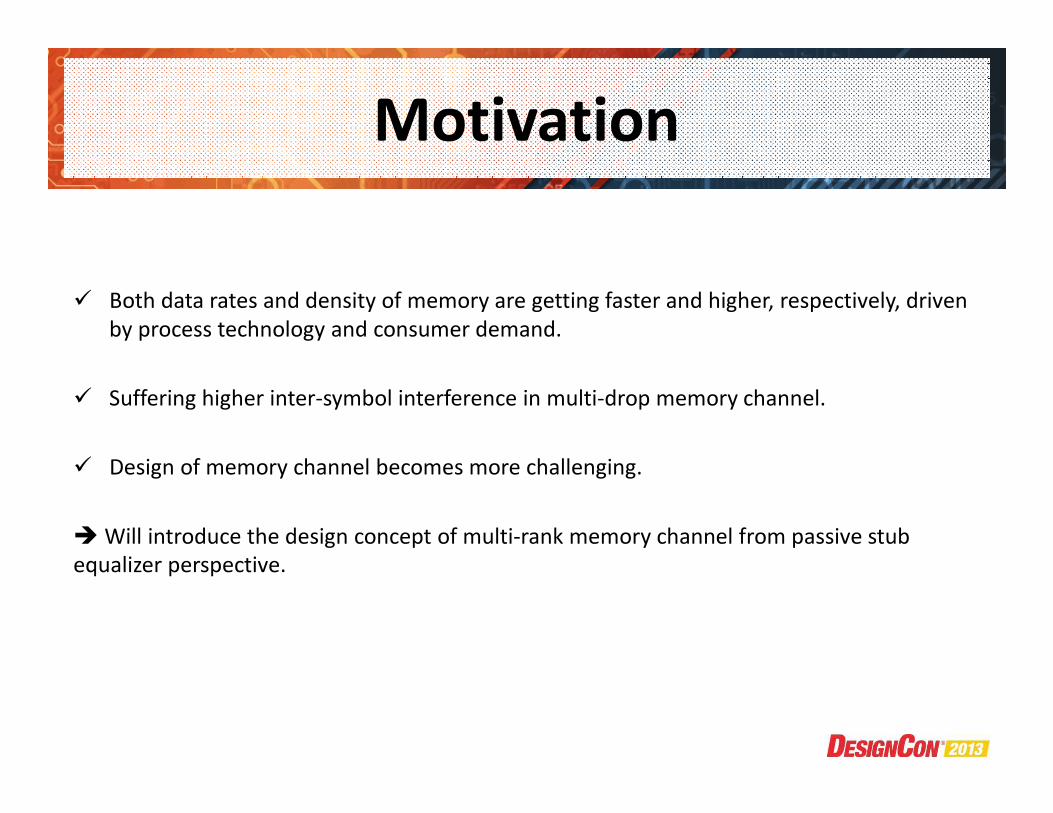
Motivation
� Both data rates and density of memory are getting faster and higher, respectively, driven
by process technology and consumer demand.
� Suffering higher inter-symbol interference in multi-drop memory channel.
� Design of memory channel becomes more challenging.
� Will introduce the design concept of multi-rank memory channel from passive stub
equalizer perspective.
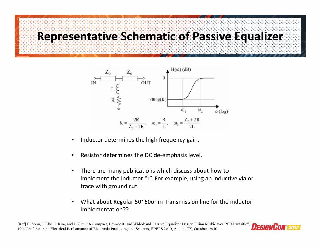
Representative Schematic of Passive Equalizer
[Ref] E. Song, J. Cho, J. Kim, and J. Kim, “A Compact, Low-cost, and Wide-band Passive Equalizer Design Using Multi-layer PCB Parasitic”,
19th Conference on Electrical Performance of Electronic Packaging and Systems, EPEPS 2010, Austin, TX, October, 2010
• Inductor determines the high frequency gain.
• Resistor determines the DC de-emphasis level.
• There are many publications which discuss about how to
implement the inductor “L”. For example, using an inductive via or
trace with ground cut.
• What about Regular 50~60ohm Transmission line for the inductor
implementation??
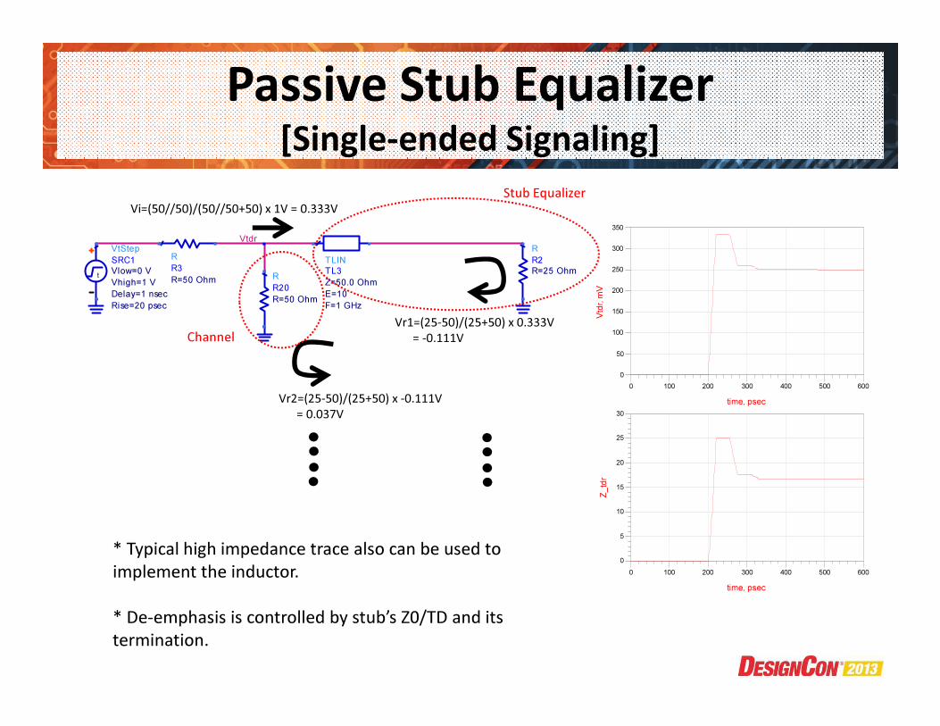
Passive Stub Equalizer [Single-ended Signaling]
VtdrVtStep
SRC1
Rise=20 psec
Delay=1 nsec
Vhigh=1 V
Vlow=0 Vt
R
R2
R=25 Ohm
TLIN
TL3
F=1 GHz
E=10
Z=50.0 OhmR
R20
R=50 Ohm
R
R3
R=50 Ohm
100 200 300 400 5000 600
50
100
150
200
250
300
0
350
time, psec
Vtd
r, m
V
100 200 300 400 5000 600
5
10
15
20
25
0
30
time, psec
Z_td
r
* Typical high impedance trace also can be used to
implement the inductor.
* De-emphasis is controlled by stub’s Z0/TD and its
termination.
Vi=(50//50)/(50//50+50) x 1V = 0.333V
Vr1=(25-50)/(25+50) x 0.333V
= -0.111V
Vr2=(25-50)/(25+50) x -0.111V
= 0.037V
Channel
Stub Equalizer
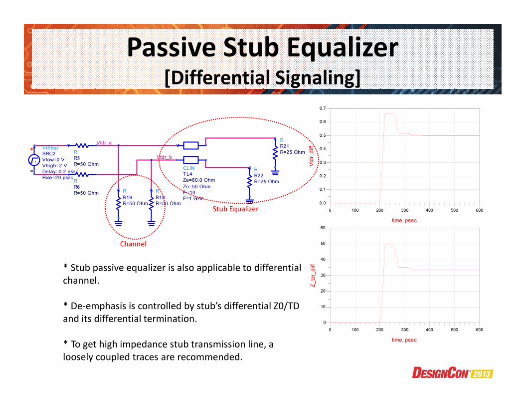
Passive Stub Equalizer [Differential Signaling]
100 200 300 400 5000 600
0.1
0.2
0.3
0.4
0.5
0.6
0.0
0.7
time, psec
Vtdr_diff
100 200 300 400 5000 600
10
20
30
40
50
0
60
time, psec
Z_tdr_diff
Vtdr_a
Vtdr_b
VtStep
SRC2
Rise=20 psec
Delay=0.2 nsec
Vhigh=2 V
Vlow=0 Vt
R
R18
R=50 Ohm
R
R19
R=50 Ohm
R
R21
R=25 Ohm
R
R22
R=25 Ohm
CLIN
TL4
F=1 GHz
E=10
Zo=50 Ohm
Ze=60.0 OhmR
R6
R=50 Ohm
R
R5
R=50 Ohm
Channel
Stub Equalizer
* Stub passive equalizer is also applicable to differential
channel.
* De-emphasis is controlled by stub’s differential Z0/TD
and its differential termination.
* To get high impedance stub transmission line, a
loosely coupled traces are recommended.

Stub Termination Impacts
100 to 10ohm (10ohm step)
100 to 10ohm (10ohm step)
50ohm
50ohm
100ohm
10mm
* Stub-termination has to be smaller than the stub
trace’s characteristic impedance to be an equalizer.
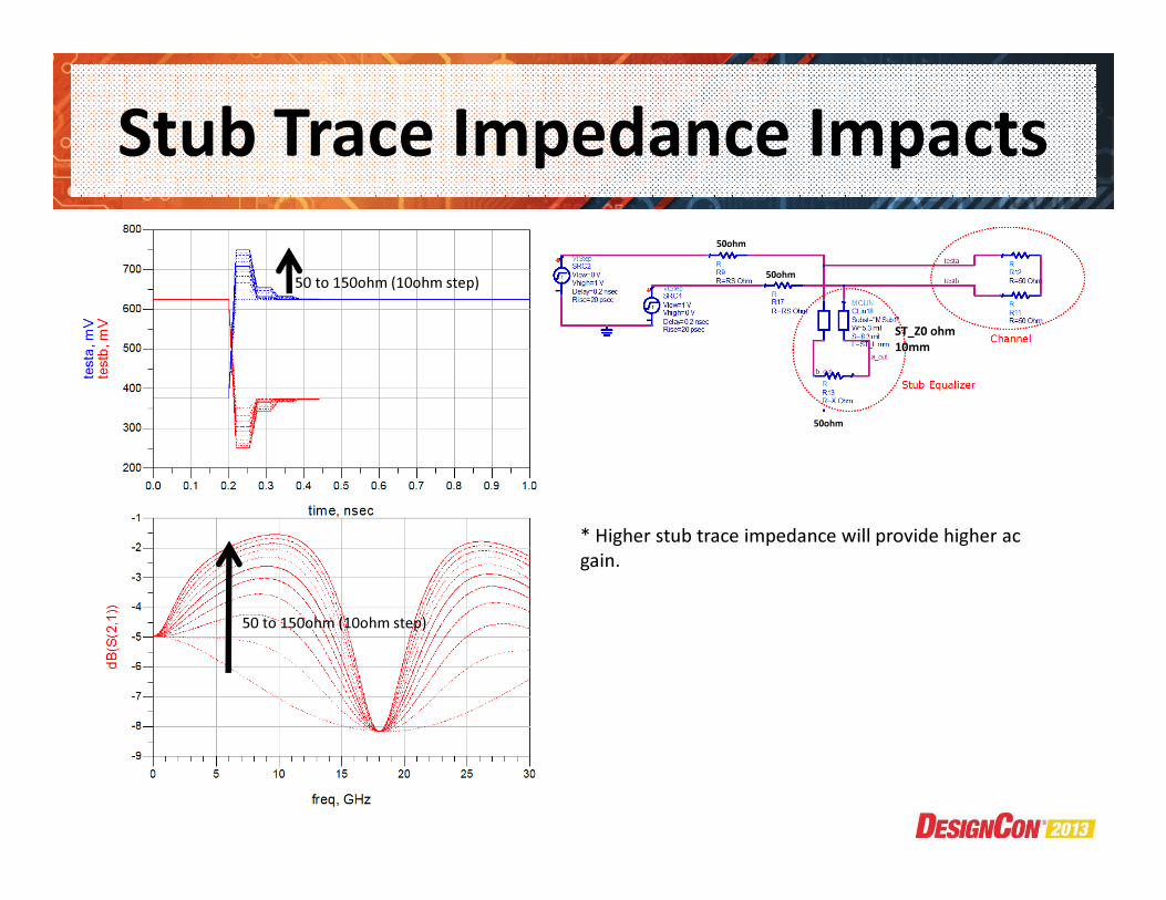
Stub Trace Impedance Impacts
50 to 150ohm (10ohm step)
50 to 150ohm (10ohm step)
50ohm
50ohm
ST_Z0 ohm
10mm
50ohm
* Higher stub trace impedance will provide higher ac
gain.
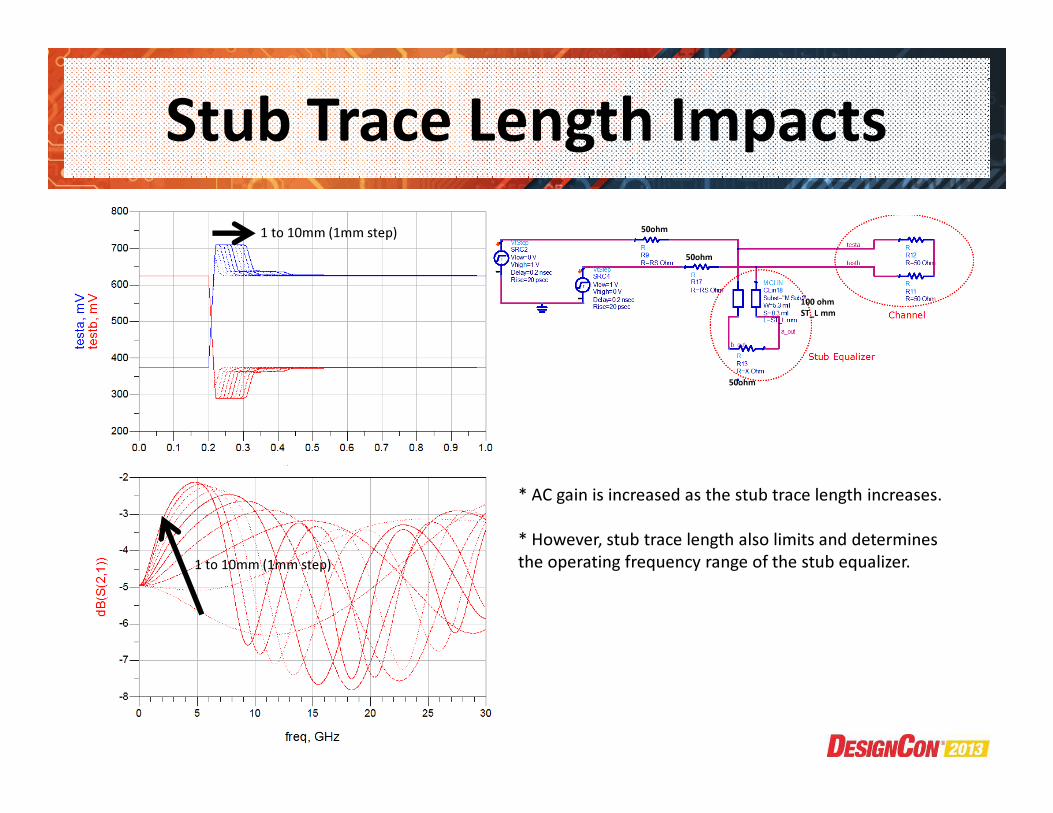
Stub Trace Length Impacts
1 to 10mm (1mm step)
1 to 10mm (1mm step)
50ohm
50ohm
100 ohm
ST_L mm
50ohm
* AC gain is increased as the stub trace length increases.
* However, stub trace length also limits and determines
the operating frequency range of the stub equalizer.
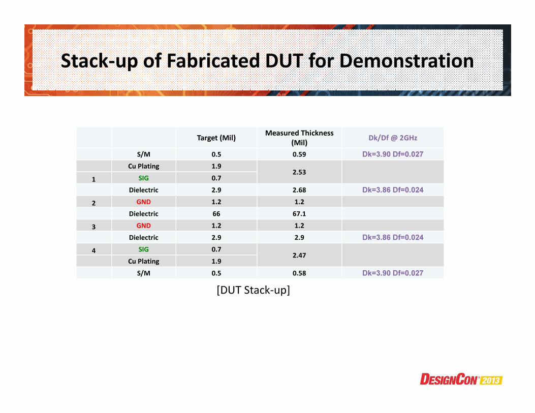
Stack-up of Fabricated DUT for Demonstration
Target (Mil)Measured Thickness
(Mil)Dk/Df @ 2GHz
S/M 0.5 0.59 Dk=3.90 Df=0.027
Cu Plating 1.92.53
1 SIG 0.7
Dielectric 2.9 2.68 Dk=3.86 Df=0.024
2 GND 1.2 1.2
Dielectric 66 67.1
3 GND 1.2 1.2
Dielectric 2.9 2.9 Dk=3.86 Df=0.024
4 SIG 0.72.47
Cu Plating 1.9
S/M 0.5 0.58 Dk=3.90 Df=0.027
[DUT Stack-up]

Patterns in Fabricated DUT for Demonstration
SMP
SMP SMP
SMP
SMP
SMP
SMP
SMP
30ohm (0402 size)
112 Ohm,
500mil long,
uncoupled Diff.
SMP
SMP
SMP
SMP
20ohm (0402 size)
112 Ohm,
500mil long,
uncoupled Diff.
3D viewSMP
SMP
SMP
SMP
20/30ohm (0402 size)
112 Ohm,
500mil long,
uncoupled Diff.
SMP
SMP
SMP
SMP
20 in SMP
SMP
SMP
SMP
100Ohm, 1.5 inch long
Resistor
Pad
[100ohms, 21.5inch-long Differential Trace]
0.75 in 0.75 in
30 in
0.75 in 0.75 in
[100ohms, 31.5inch-long Differential Trace]
[100ohms, 21.5inch-long Differential Trace with EQ] [100ohms, 31.5inch-long Differential Trace with EQ]
20 in
0.75 in 0.75 in
30 in
0.75 in 0.75 in
[100ohms, 1.5inch-long Differential Trace with EQ]

Layout of DUT
20in without EQ
20in with EQ
30in without EQ
30in with EQ
EQ Only
* Resistor (0402 size)
- 30ohm for 20in long
- 20ohm for 30in long

Modeling of DUT
[Model in HFSS] [Model in HFSS]
2D2D 2D
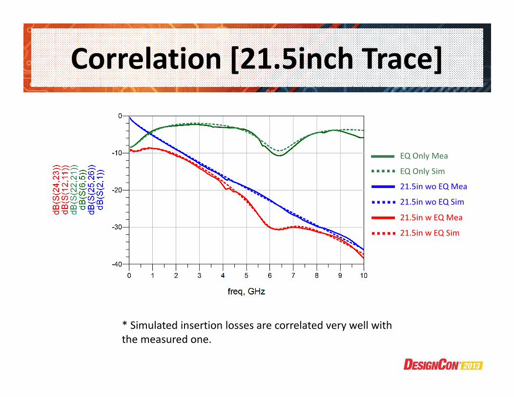
Correlation [21.5inch Trace]
EQ Only Mea
EQ Only Sim
21.5in wo EQ Mea
21.5in wo EQ Sim
21.5in w EQ Mea
21.5in w EQ Sim
* Simulated insertion losses are correlated very well with
the measured one.

Correlation [31.5inch Trace]
EQ Only Mea
EQ Only Sim
31.5in wo EQ Mea
31.5in wo EQ Sim
31.5in w EQ Mea
31.5in w EQ Sim
* Simulated insertion losses are correlated very well with
the measured one.

Time-Domain Correlation for 6Gbps Signaling
Simulated Model
Vs.
Measured Model
* The frequency-domain models from simulations and measurements were
used for the 6 Gbps time-domain simulation.
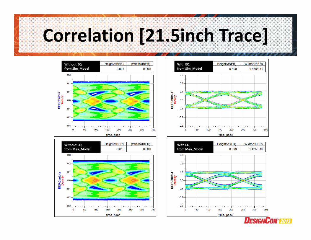
Correlation [21.5inch Trace]
Without EQ
from Sim_Model
With EQ
from Sim_Model
Without EQ
from Mea_Model
With EQ
from Mea_Model
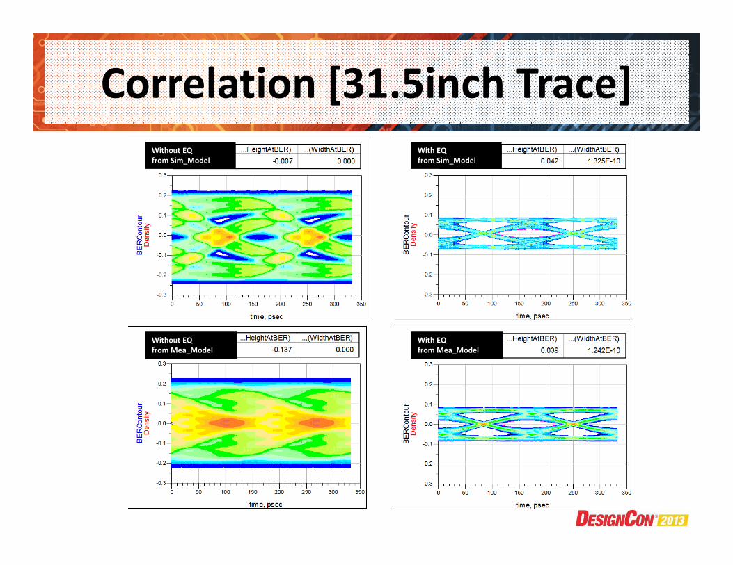
Correlation [31.5inch Trace]
Without EQ
from Sim_Model
With EQ
from Sim_Model
Without EQ
from Mea_Model
With EQ
from Mea_Model

Agenda
1. Introduction
2. Passive Stub Equalizer
– Basic Principles of Passive Stub Equalizer
– Control of Passive Stub Equalizer
– Demonstration of Passive Stub Equalizer through Simulation and Measurement
3. Application of EQ Design Concept to Memory Channel
– [On-board Termination] LPDDR3 CA Channel
– [On-die Termination] DDR4 DQ Channel
4. Summary
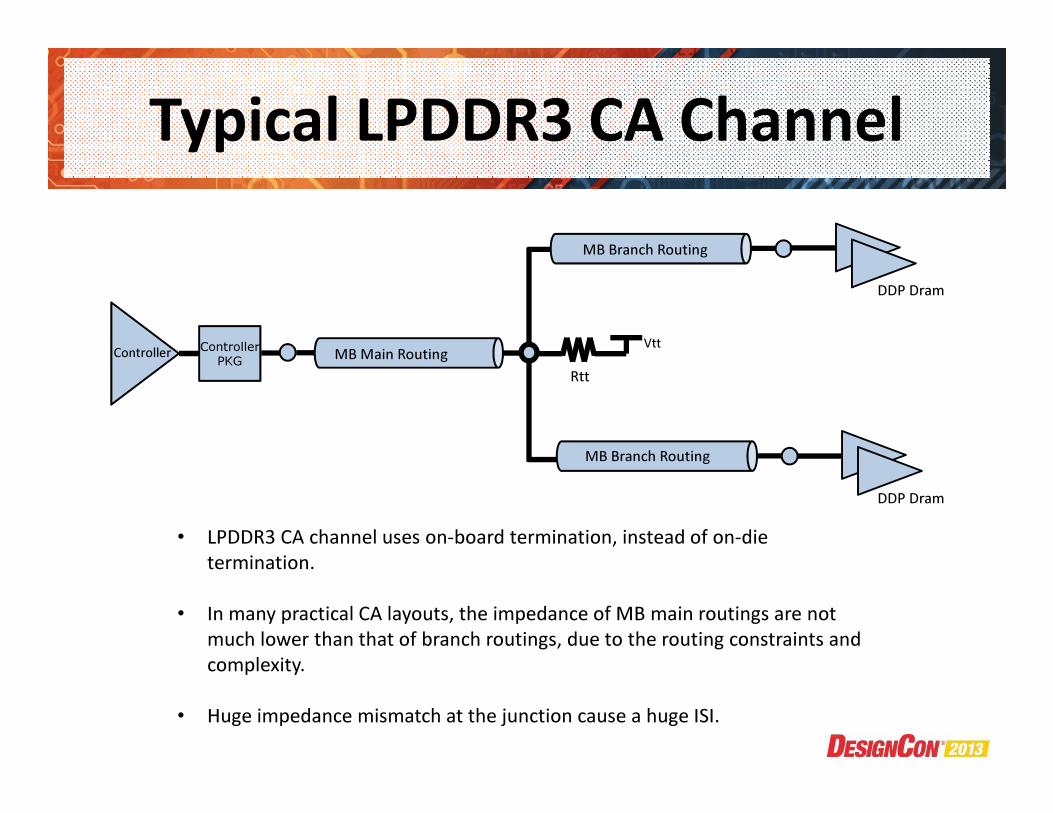
Typical LPDDR3 CA Channel
• LPDDR3 CA channel uses on-board termination, instead of on-die
termination.
• In many practical CA layouts, the impedance of MB main routings are not
much lower than that of branch routings, due to the routing constraints and
complexity.
• Huge impedance mismatch at the junction cause a huge ISI.
Controller
PKG
Vtt
Rtt
MB Main Routing
MB Branch Routing
MB Branch Routing
Controller
DDP Dram
DDP Dram

Layout Example of On-board Termination
OBT
• OBT is directly connected at
the location of the junction
for all CA signals.
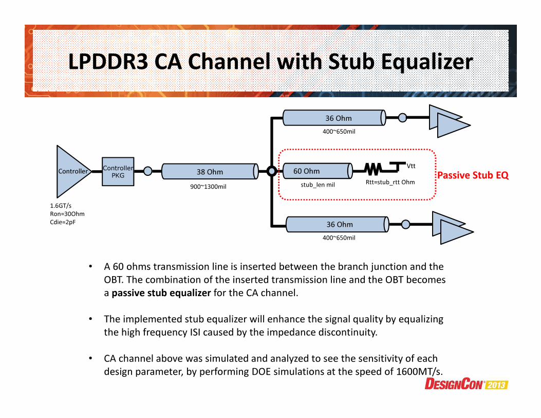
LPDDR3 CA Channel with Stub Equalizer
Controller
PKG
Vtt
900~1300mil
400~650mil
stub_len mil
1.6GT/s
Ron=30Ohm
Cdie=2pF
Rtt=stub_rtt Ohm
38 Ohm
36 Ohm
36 Ohm
60 OhmPassive Stub EQ
Controller
400~650mil
• A 60 ohms transmission line is inserted between the branch junction and the
OBT. The combination of the inserted transmission line and the OBT becomes
a passive stub equalizer for the CA channel.
• The implemented stub equalizer will enhance the signal quality by equalizing
the high frequency ISI caused by the impedance discontinuity.
• CA channel above was simulated and analyzed to see the sensitivity of each
design parameter, by performing DOE simulations at the speed of 1600MT/s.
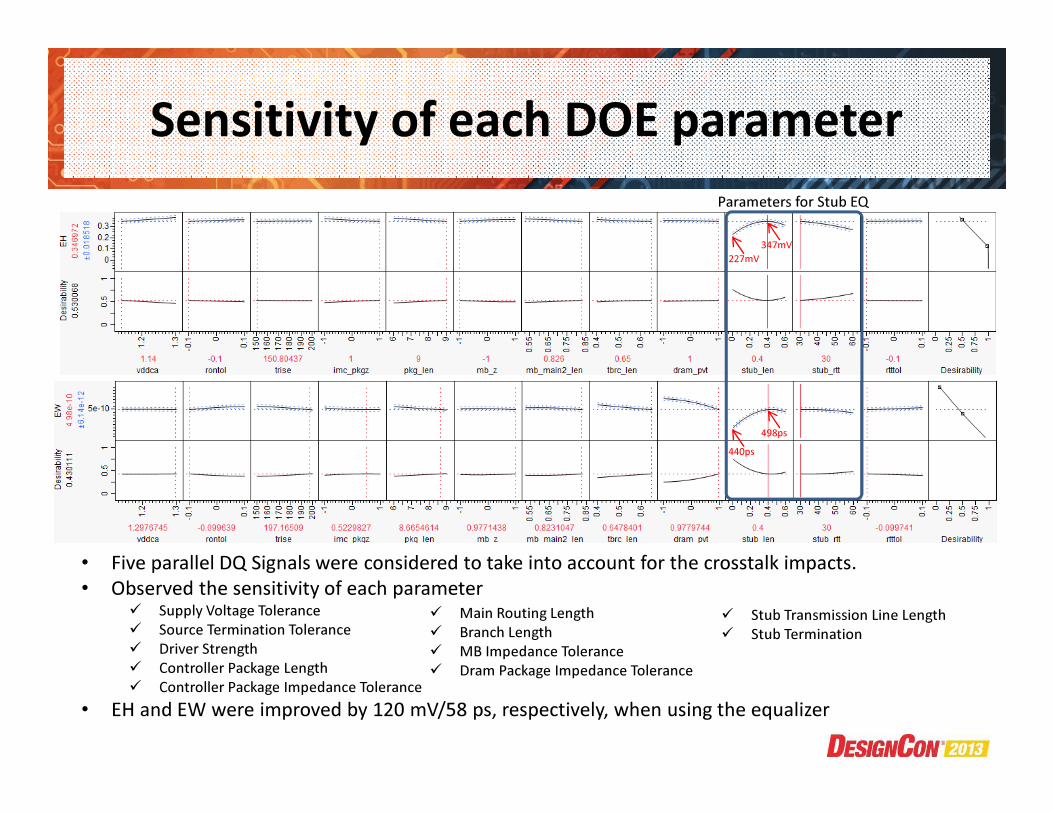
Sensitivity of each DOE parameter
• Five parallel DQ Signals were considered to take into account for the crosstalk impacts.
• Observed the sensitivity of each parameter� Supply Voltage Tolerance
� Source Termination Tolerance
� Driver Strength
� Controller Package Length
� Controller Package Impedance Tolerance
• EH and EW were improved by 120 mV/58 ps, respectively, when using the equalizer
� Main Routing Length
� Branch Length
� MB Impedance Tolerance
� Dram Package Impedance Tolerance
Parameters for Stub EQ
� Stub Transmission Line Length
� Stub Termination
227mV
347mV
440ps
498ps

Eye Diagrams with/without Stub trace
[0mil Stub with 30ohm Rtt] [400mil Stub with 30ohm Rtt]
VIH(AC)
VIH(DC)
PDA Eye wo Xtalk
PDA Eye w Xtalk
VIH(AC)
VIH(DC)
PDA Eye wo Xtalk
PDA Eye w Xtalk
ACDC EW=316psACDC EW=0ps
• When there is no crosstalk, the EH/EW of the worst case PDA eye diagram was improved
from 380mV/575ps to 460mV/620ps, by having the 400 mil stub transmission line.
• Even after considering the crosstalk from 4 aggressors, the worst case eye is still
improved by the amount of when there is no crosstalk.
• The channel without stub transmission line had “0ps” of ACDC EW (VIH(AC) to VIH(DC)),
while 400 mil stub transmission line introduced “316ps” of ACDC EW, which met the
LPDDR3 CA specification (175 ps) with an enough margin.

Agenda
1. Introduction
2. Passive Stub Equalizer
– Basic Principles of Passive Stub Equalizer
– Control of Passive Stub Equalizer
– Demonstration of Passive Stub Equalizer through Simulation and Measurement
3. Application of EQ Design Concept to Memory Channel
– [On-board Termination] LPDDR3 CA Channel
– [On-die Termination] DDR4 DQ Channel
4. Summary
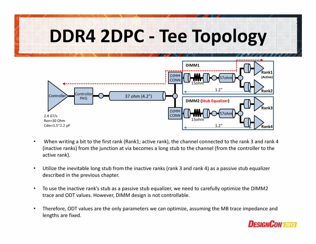
DDR4 2DPC - Tee Topology
Controller
PKG
2.4 GT/s
Ron=30 Ohm
Cdie=1.5~2.2 pF
37 ohm (4.2”)Controller
DIMM
CONN
DIMM
CONN
DIMM1
Rank1(Active)
Rank2
Rank3
Rank4
1.2”
57ohm
57ohm
1.2”
15ohm
15ohm
• When writing a bit to the first rank (Rank1; active rank), the channel connected to the rank 3 and rank 4
(inactive ranks) from the junction at via becomes a long stub to the channel (from the controller to the
active rank).
• Utilize the inevitable long stub from the inactive ranks (rank 3 and rank 4) as a passive stub equalizer
described in the previous chapter.
• To use the inactive rank’s stub as a passive stub equalizer, we need to carefully optimize the DIMM2
trace and ODT values. However, DIMM design is not controllable.
• Therefore, ODT values are the only parameters we can optimize, assuming the MB trace impedance and
lengths are fixed.
DIMM2 (Stub Equalizer)
DDR4 2DPC - Tee Topology
Transfer Function of Stub Equalizer Itself from Inactive Rank
Transfer Function of DDR4 Channel with Stub Equalizer
Transfer Function of DDR4 Channel without DIMM2 Trace
Frequency [GHz]
Inse
rti
on
Lo
ss [
dB
]
Boosted Area by Stub
Equalizer
• According to the passive stub equalizer theory, , higher
characteristic impedance of trace and lower stub
termination value increase the ac-gain and the de-
emphasis level, respectively.
• Also, the stub termination (ODT) needs to be lower than
the stub transmission line, which is mostly set to 55 ~ 60
ohms.
• Lowered the stub termination (ODT) value to 30 ohms
(parallel of two 60 ohms ODTs).
• 60 ohms ODT was used for Rank2 to avoid the open stub
impact, and 240ohms ODT for Rank1 to have enough DC
swing level at Dram.
Controller
PKG
2.4 GT/s
Ron=30 Ohm
Cdie=1.5~2.2 pF
37 ohm (4.2”)Controller
DIMM
CONN
DIMM
CONN
DIMM1
DIMM2 (Stub Equalizer)
Rank1(Active)
Rank2
Rank3
Rank4
1.2”
57ohm
57ohm
1.2”
15ohm
15ohm
240ohms
60ohms
60ohms
60ohms
* Available ODT Values in DDR4 Specification
: 240, 120, 80, 60, 48, 40, 34 ohms

DDR4 2DPC - Tee Topology
Controller
PKG
2.4 GT/s
Ron=30 Ohm
Cdie=1.5~2.2 pF
37 ohm (4.2”)Controller
DIMM
CONN
DIMM
CONN
ODT Matrix for 2DPC DQ Tee Topology Channel @ 2133MT/s
DIMM1 DIMM2 Margin At BER 10e-18
Rank1 Rank2 Rank3 Rank4 EH_Margin EW_Margin
WR to Rank1 240ohm 60ohm 60ohm 60ohm 17mV 118ps
RD from Rank1 50ohm (Ron) 60ohm 60ohm 60ohm 35mV 83ps
ODT Matrix for 2DPC DQ Tee Topology Channel @ 2400MT/s
DIMM1 DIMM2 Margin At BER 10e-18
Rank1 Rank2 Rank3 Rank4 EH_Margin EW_Margin
WR to Rank1 240ohm 60ohm 60ohm 60ohm -5mV 76ps
RD from Rank1 50ohm (Ron) 60ohm 60ohm 60ohm 10mV 72ps
DIMM1
DIMM2 (Stub Equalizer)
Rank1(Active)
Rank2
Rank3
Rank4
1.2”
57ohm
57ohm
1.2”
15ohm
15ohm
240ohms
60ohms
60ohms
60ohms
* Available ODT Values in DDR4 Specification
: 240, 120, 80, 60, 48, 40, 34 ohms
• Full channel eye diagram simulation was performed
with 8 parallel DQ signals for WC crosstalk
consideration at both 2133 MT/s and 2400 MT/s.
• The optimized channel passed the DDR4 specification
[6] with a 17 mV/118 ps margin in write-mode EH/EW
and a 35 mV/83 ps margin in read-mode EH/EW for
2133 MT/s speed, with a -5 mV/76 ps margin in write-
mode EH/EW and a 10 mV/72 ps margin in read-mode
EH/EW.

Agenda
1. Introduction
2. Passive Stub Equalizer
– Basic Principles of Passive Stub Equalizer
– Control of Passive Stub Equalizer
– Demonstration of Passive Stub Equalizer through Simulation and Measurement
3. Application of EQ Design Concept to Memory Channel
– [On-board Termination] LPDDR3 CA Channel
– [On-die Termination] DDR4 DQ Channel
4. Summary

Summary
� Presented the basic concept of the passive stub equalizer, which can be easily
implemented on package or board level.
� Presented three design parameters to enable the passive stub equalizer.
� Demonstrated the performance of the passive stub equalizer through both
simulation and measurement in frequency and time domain.
� Presented a design example for the adoption of the passive stub equalizer design
concept to 1600 MT/s 4-ranks LPDDR3 command/address signal.
� Presented a design example for the adoption of the passive stub equalizer design
concept to 2400 MT/s 4-ranks DDR4 DQ signal.
Q & A