DC Wind Turbine Circuit with Series‐ Resonant …...be replaced by a series-resonant DC-DC...
80
DC Wind Turbine Circuit with Series‐ Resonant DC/DC Converter Mario Zaja Supervisor: Philip Carne Kjær
Transcript of DC Wind Turbine Circuit with Series‐ Resonant …...be replaced by a series-resonant DC-DC...
DC Wind Turbine Circuit with Series‐
Resonant DC/DC Converter
Mario Zaja
Supervisor: Philip Carne Kjær


Acknowledgements
I hereby thank everybody who helped me during the period of working on this thesis. I
particularly thank my supervisor Philip Carne Kjær, PhD student Catalin Gabriel Dincan and lab
supervisor Walter Neumayr for all the assistance provided. I would also like to thank all my
university colleagues, the whole Energy Technology Department, Vestas Wind Systems with all
my co-workers there and Aalborg University in general. Special thanks goes to my friends and
family for supporting me during my stay here.


Contents
1 Abstract .................................................................................................................... 1
2 Summary .................................................................................................................. 2
3 Introduction.............................................................................................................. 3
3.1 Goal, problem definition and methodology ..................................................... 5
4 DC-DC series-resonant converter circuit .................................................................. 6
4.1 Equivalent circuit model ................................................................................... 6
4.2 Steady-state analysis ...................................................................................... 11
4.2.1 Input and output voltage .......................................................................... 12
4.2.2 Input voltage and switching frequency .................................................... 14
4.2.3 Output voltage and switching frequency ................................................. 18
4.2.4 Inductance and capacitance ..................................................................... 18
4.2.5 Frequency and duty cycle ......................................................................... 22
4.3 Discontinuous conduction mode .................................................................... 25
4.4 Power relations ............................................................................................... 34
4.5 Loss estimation ............................................................................................... 38
5 Resonant converter design .................................................................................... 42
5.1 Component selection ...................................................................................... 42
5.2 Control system ................................................................................................ 45
6 Model validation .................................................................................................... 53
6.1 Laboratory setup ............................................................................................. 53
6.2 Simulation results ........................................................................................... 61
6.3 Experimental results ....................................................................................... 65

7 Conclusion .............................................................................................................. 69
8 List of abbreviations ............................................................................................... 71
9 References .............................................................................................................. 72
10 Appendix ............................................................................................................. 74

1
1 Abstract
Offshore wind farms are connected to land by HVDC cables, with voltage source
converters placed at both ends. The power output of each turbine is collected as AC at a
medium voltage level, meaning that each turbine has to contain an AC-DC-AC converter. A
promising approach to reduce the size of related power conversion equipment and conversion
losses is to make each of the turbines output power as DC at a medium voltage level, which
can then be collected and stepped up at a HVDC platform. The turbine DC-AC converter could
be replaced by a series-resonant DC-DC converter using a medium-frequency transformer to
step up the voltage. The main benefit of operating in a higher frequency range is the reduction
in size and weight of the equipment used. However, the new approach also brings additional
challenges, such as the relatively narrow operating range of such a converter and high voltage
and current stress on its components. This document contains theoretical analysis of such a
circuit, component selection, control system design and circuit validation, both by simulation
and a downscale hardware setup.

2
2 Summary
This document is a 10th semester Master Thesis of the Master program in Power
Electronics and Drives at Aalborg University, made in collaboration with Vestas Wind Systems
A/S. For easier readability, the contents of each section have been briefly summarized.
Introduction contains general motivation for the project, project scope and goal,
problem definition and a brief description of the development procedure.
DC-DC series-resonant converter circuit section contains in depth analysis of the
converter topology and its electrical properties, obtained both analytically and using
simulation software. The section analyzes the impact of various design variables on the
circuit’s behavior and gives general converter design guidelines.
Resonant converter design contains a 10 MW circuit proposal based on the findings of
the previous section, including a corresponding control system and auxiliary circuits.
Model validation contains a description of the downscale lab prototype setup, loss
estimation of the same circuit made in Plecs and a comparison between the waveforms
obtained in simulation and on an actual setup.
Conclusion contains an overview of the most important points stated in the report.
List of abbreviations contains an explanation of all the abbreviations used in the report.
References section contains a list of all the external sources used in the report.
Appendix contains a list of supplementary contents available on the attached CD,
including the developed analysis tool, simulation models, plot catalogue and device
datasheets.
The most important findings of main chapters (4, 5 and 6) have been additionally
summarized at the end of each chapter to make it easier to follow the report.

3
3 Introduction
Offshore wind power is at the moment the most competitive renewable energy source
[1] and therefore under a great focus over the last several years. Compared to on-shore wind
power technologies, offshore solutions feature a lower levelized cost of energy and a lot higher
power output per turbine, which can reach up to 10 MW at the present day. Handling those
great amounts of energy presents many new challenges, and the initiative to reduce the costs
even further and increase competitiveness is very strong.
The state-of-the-art offshore wind farm is shown in Figure 1. Wind turbines are
connected to a MVAC bus leading to the platform containing the HV transformer. The output
power of the HV transformer is transferred through the HVAC cable to a rectifier station on
another platform, where AC-DC conversion is made. Finally, the power of the whole wind park
is transferred to the shore via a HVDC cable, where another DC-AC conversion is performed
and grid connection established.
Figure 1 - State-of-the-art offshore wind farm
There are several downsides of this approach. First, to be able to connect to the MVAC
bus, each of the turbine has to have its own AC-DC-AC converter and a MV transformer.
Second, the HV transformer substation operates at a 50/60 Hz frequency and needs to be able

4
to handle the total power output from all the MVAC busses connected to it, meaning that it
will be large and heavy and therefore require a separate platform to support it. Reliability is
also an issue since a fault on the HV transformer would bring the power production from all
the turbines connected to it to a halt. Finally, another large transformer is required on the
second platform containing the AC-DC converter, having the same issues as previously
discussed. The power is converter several times before reaching the shore, resulting in
significant conversion losses.
Figure 2 - The proposed offshore wind farm layout
The proposed wind farm solution is shown in Figure 2. Here, the line DC-AC inverter
and a HV transformer have been replaced by a DC-DC converter using a MF transformer. The
output of all turbines is collected as MVDC and connected to a DC-DC substation for stepping
up the voltage and transferring it to the shore via a HVDC cable. The main benefit of this
approach is performing the LVDC/MVDC conversion at a much higher frequency, resulting in
significant reduction of the equipment’s size and weight, which can now be stored in each of
the turbines. As a consequence, this approach completely eliminates the need for an offshore
platform carrying the HV transformer, significantly reducing the costs and improving reliability.

5
3.1 Goal, problem definition and methodology
The goal of this project is to analyze, design and validate a series-resonant DC-DC
converter circuit, as well as its corresponding control system. 10 MW and 150 W circuit
proposals will be made, of which the latter will be used to experimentally validate the results.
There are several challenges to overcome in the circuit design process:
The resonant tank’s response is nonlinear to the change of driving signal’s
frequency
The circuit’s response sensitivity increases as the frequency approaches its
resonant value, which might render the system unstable
The resonant tank components are subject to very high voltage and current
stress even during normal operation
The additional components, such as the medium-frequency transformer or the
smoothening capacitors, can have a significant impact on the circuit’s
frequency response
Circuit analysis and control system design tasks will be performed both analytically and
using computer simulation tools Plecs and Matlab. The purpose of experimental verification
will be to evaluate the voltage and current waveforms obtained by lab prototype simulation.
Experimental verification will be carried out on a real hardware setup containing a full bridge
converter, resonant tank, medium frequency transformer, passive rectifier and a signal
generator to manually control the circuit in open loop.

6
4 DC-DC series-resonant converter circuit
4.1 Equivalent circuit model
A principal series-resonant DC-DC converter (SRC) circuit is shown in Figure 3.
Figure 3 - Simple DC-DC series-resonant converter schematic
The circuit consists of a controllable full bridge converter, a resonant LC tank, a MF
transformer and a passive full bridge diode rectifier. To simplify the analysis, it will be assumed
that both of the converter terminals have ideal voltage sources connected to them, meaning
they provide constant load voltage independent of the current. The MF transformer is ideal
with a transfer ratio of 1:1. Resonant tank components are also ideal, being purely reactive
and having no saturation. Finally, the power converter and diode rectifier are ideal as well,
switching instantaneously and having no losses.
The circuit is controlled by giving a set of pulses to the converter and producing a
square wave voltage at its output. The resonant tank rings with the frequency of the square
wave, producing an AC current. The current passes through the transformer windings, creating
an alternating magnetic field and thus inducing the voltage on the secondary side. Finally, the
secondary AC current produced is rectified in the passive diode rectifier and fed into the active
load.
The input voltage waveform is a square wave with either positive or negative value of
the magnitude of the input voltage. Assuming the square wave is symmetrical, its spectrum is
given by

7
𝑣𝑠(𝑡) =4 𝑉𝑖𝑛
𝜋∑
1
𝑛sin(2𝑛𝜋𝑓𝑠𝑡)
𝑛=1,3,5…
(1)
Where 𝑉𝑖𝑛 is the input voltage and 𝑓𝑠 the frequency of the square wave. Ideal resonant
tank's admittance can be expressed as
𝑌𝑡𝑎𝑛𝑘 =𝑠𝐶
𝑠2𝐿𝐶 + 1 (2)
The Bode diagram of a generic resonant tank’s admittance described by (2) is shown in
Figure 4.
Figure 4 - Bode diagram of a generic resonant tank
From the amplitude plot it is visible that the resonant tank acts like a narrow band pass
filter. This means that the resonant tank only responds to the fundamental component while
all the higher order harmonics from (1) are attenuated and have no practical impact on the
resonant tank current. Therefore the converter’s output terminal can be modelled as an ideal
sinusoidal voltage source with

8
𝑣𝑠(𝑡) =4 𝑉𝑖𝑛
𝜋sin(2𝜋𝑓𝑠𝑡) (3)
The frequency at which the resonant tank’s admittance becomes infinite, also shown
as 1 p.u. on the Bode plot, is called the resonant frequency and can be calculated as
𝑓𝑟𝑒𝑠 =1
2𝜋√𝐿𝐶 (4)
As visible from the Bode plot, the band pass region gain is virtually symmetrical around
the resonant frequency, but the phase changes from +90° to -90°. This means that in the sub-
resonant region the tank performs capacitive, while in the super-resonant region it becomes
inductive. This also demonstrates the basic control principle of resonant conversion – the
admittance, and therefore the amplitude of the AC current, can be controlled by adjusting the
square wave frequency around the resonance region.
As stated before, the current through the resonant tank can be viewed as pure
sinusoidal. This current will have a certain phase offset 𝜑𝑠 with respect to the converter output
voltage, which can be expressed as
𝑖𝑠(𝑡) = 𝐼𝑠 sin (2𝜋𝑓𝑠𝑡 + 𝜑𝑠) (5)
𝜑𝑠 can be both positive and negative, depending on whether the converter operates
in the capacitive or the inductive mode. If the switching frequency equals the resonant
frequency, 𝜑𝑠 = 0.
The current waveform drawn by the converter is shown in Figure 5.

9
Figure 5 - Input current waveform and its mean value
Averaging the current over one switching period gives
⟨𝑖𝑖𝑛(𝑡)⟩𝑇𝑠=
2
𝜋 𝐼𝑠 cos (𝜑𝑠) (6)
Therefore, the input port of the switch network can be modelled as a DC current source
as described by (6).
The voltage at the rectifier’s input port is determined by the resonant tank current. As
the load is an ideal DC voltage source, the voltage at the rectifier’s input port is a square wave
in phase with the resonant tank current. However, since the resonant tank responds only to
the fundamental component, the rectifier’s input port can also be modelled as a sinusoidal
voltage source.
𝑣𝑟(𝑡) =4 𝑉𝑜𝑢𝑡
𝜋 sin (2𝜋𝑓𝑠𝑡 + 𝜑𝑠) (7)
Finally, the full bridge diode rectifier outputs a rectified sinusoidal current waveform
to the active DC load. The average current value over one switching period is calculated as
10
⟨𝑖𝑜𝑢𝑡(𝑡)⟩𝑇𝑠=
2
𝜋 𝐼𝑠 (8)
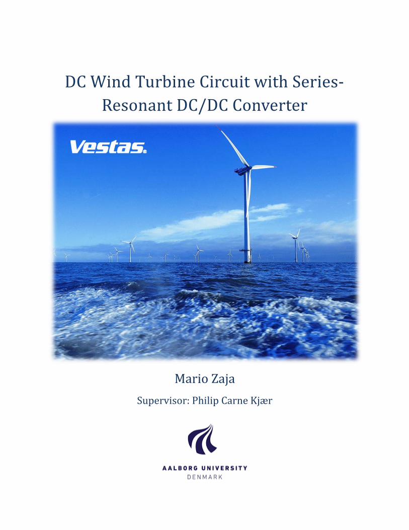
Using the results from (3), (6) - (8), an equivalent series-resonant converter circuit can
be constructed. The result is shown in Figure 6.
Figure 6 - Equivalent electrical circuit of a series-resonant DC-DC converter

11
4.2 Steady-state analysis
This section analyzes the natural response of an ideal DC-DC converter circuit depicted
in Figure 3. All the earlier mentioned limitations still apply. The resonant tank elements had
been chosen according to two criteria – to have the resonant frequency of 5000 Hz and
characteristic impedance of 1 Ω. The characteristic impedance is given by
𝑍𝐿𝐶 = √𝐿
𝐶 (9)
In other words, the 𝐿 and 𝐶 values had been chosen in such a way that 𝐿 = 𝐶. This was
done for no other reason but to simply the per-unit analysis. The full list of per-unit base values
is given in Table 1.
Table 1 - List of base values for per-unit analysis
Base unit Base unit value
𝑽𝒃𝒂𝒔𝒆 1 V
𝑷𝒃𝒂𝒔𝒆 10 W
𝑰𝒃𝒂𝒔𝒆 10 A
𝒇𝒃𝒂𝒔𝒆 5000 Hz
𝑳𝒃𝒂𝒔𝒆 31.831 µH
𝑪𝒃𝒂𝒔𝒆 31.831 µF
In all of the simulation runs, the output, inductor, IGBT and diode currents and
capacitor voltage waveforms had been captured and analyzed. However, due to limited
amount of space in the report, only several selected plots have been shown. The full plot
catalogue is located on the attached CD.

12
4.2.1 Input and output voltage
The first set of figures depicts how the monitored quantities change as the input and
output voltages change. This analysis is important as the actual voltages on both ends of the
converter will change during normal operation, typically within range of ± 10%. In this
simulation set, the switching frequency was kept constant at 0.96 p.u. with a duty cycle of 1.
Each point is evaluated at the steady state.
Figure 7 - Output current dependence on input and output voltage changes
The dark blue region in Figure 7 shows the case when the output voltage is above the
input voltage. As the output side of the converter is connected through a full bridge diode
rectifier, the current, and thus the power, can only flow in one direction, from the input to the
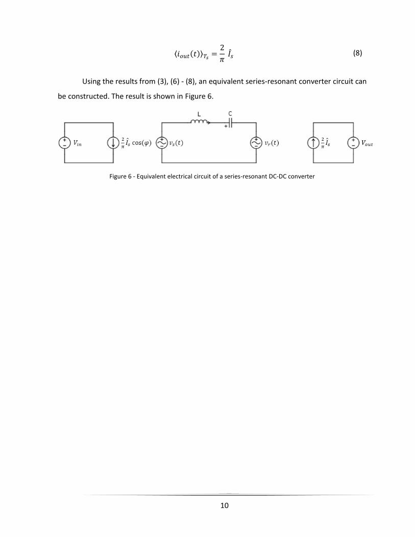
output. The boundary condition for this state is
𝑉𝑖𝑛 = 𝑉𝑜𝑢𝑡 (10)
For all the values where
13
𝑉𝑖𝑛 ≤ 𝑉𝑜𝑢𝑡 (11)
, all the rectifier diodes are reverse-biased and thus the converter is inoperable.
Therefore, the necessary condition for normal converter operation is given by
𝑉𝑖𝑛 > 𝑉𝑜𝑢𝑡 (12)
It is of highest importance in the resonant converter design that (12) is valid at all
times. This property will therefore directly influence the choice of the transformer transfer
ratio. For this purpose it is useful to define the DC voltage transfer ratio as
𝑘𝑣 =𝑉𝑖𝑛
𝑉𝑜𝑢𝑡 (13)
Analyzing the results further, it is visible that the relationship between the voltage
transfer ratio and output current is not linear. This property is more clearly displayed in Figure
8.
Figure 8 - Relationship between the voltage transfer ratio and the average output current
In the region where 𝑘𝑣 ≈ 1, the dependence between the voltage transfer ratio and
the output current value is strongly nonlinear, putting additional requirements on the control

14
system design. Drifting further away from the boundary region, the relationship becomes
more and more linear.
Figure 9 - Inductor current waveforms for different values of the voltage transfer ratio
The reason for this nonlinear behavior is shown in Figure 9. When the factor 𝑘𝑣 is
sufficiently small, the converter enters discontinuous conduction mode (DCM), as represented
by the red line. The figure also shows that the actual current waveforms are not purely
sinusoidal even in the continuous conduction mode (CCM). However, as the voltage transfer
ratio increases, the inductor current resembles the pure sine wave more and more closely.
4.2.2 Input voltage and switching frequency
This simulation set shows how altering the input voltage and switching frequency
affects the circuit’s behavior. The output voltage was kept constant at 1 p.u., which means
that the 𝑉𝑖𝑛 value can also be interpreted as 𝑘𝑣. The rest of the parameters were the same as
in the previous simulation runs.

15
Figure 10 - Output current dependence on input voltage and switching frequency changes
Overall, the frequency was varied from 0.9 to 0.99 p.u. As already mentioned and
shown in the Bode plot in Figure 4, the resonant tank’s admittance is a function of the applied
signal’s frequency and that is the key property used to control the resonant power converters.
As the signal’s frequency gets closer to the resonant frequency, the slope of the curve gets
steeper. For an ideal, lossless circuit, the tank has infinite admittance at the resonant
frequency.
The theoretical model corresponds well with the obtained simulation results, as shown
in Figure 10. For a constant voltage transfer ratio, the output current magnitude is
proportional to the tank’s admittance. The shape of the curves describing the change of the
output current magnitude along the lines of a constant voltage transfer ratio can be described
by a rational function as
𝑦 = |𝑎1𝑥
1 − 𝑎2𝑥2| (14)
, where 𝑎1 and 𝑎2 are arbitrary constants. This corresponds to the shape of the
resonant tank’s admittance curve depicted in Figure 4.

16
Figure 11 - Inductor current dependence on input voltage and switching frequency changes
The main property to be observed from Figure 11 and Figure 12 is a major increase in
component stress when operating close to the resonance region. Since series topology is used,
this increase is naturally proportional to the average output current, and thus the output
power. Two of the key parameters to be considered in the resonant tank design process are
the inductor current and capacitor voltage values in steady state. Overall, the voltage and
current ratings of these two components will define the maximum power that can be
transferred through the circuit.

17
Figure 12 - Capacitor voltage dependence on LVDC voltage and switching frequency changes
The voltage stress of the components is particularly important to observe in this case.
At the frequency of 0.9 p.u. and 𝑉𝑖𝑛 value of 1.08, the RMS value of the capacitor voltage
equals 2.65 p.u. At the same time, at the frequency of 0.99 p.u., the voltage value rises to 18.9
p.u., which is more than a sevenfold increase caused by a 10% frequency change. This clearly
indicates two things. First, the resonant tank components will need to be rated to a lot higher
voltage level than the turbine’s DC output, meaning that their cost might be dominant in the
overall price of the solution. This will likely impose many design restrictions on both the lab
prototype and full scale solution. Second, sensitivity of the controller has to be very high to
operate the circuit close to the resonant region. This means that all the measurement,
quantization, discretization and all other types of numerical errors will have an increased
impact on the control system and might cause overloading of the components. To prevent this
from happening, several types of hard-stop protection will need to be implemented.
However, not only the increase in frequency significantly increases the voltage and
current stress, but it also increases the circuit’s sensitivity to voltage changes. This is more
closely shown in Figure 13.

18
Figure 13 - The impact of voltage transfer ratio change at different switching frequencies
The closer the switching frequency to the resonant, the higher will the impact of the
voltage transfer ratio change be, which is a natural consequence of increasing the resonant
tank’s admittance. This imposes new challenges on the circuit design, as the voltage transfer
ratio will change unpredictably in the real converter, which could cause a sudden and
uncontrolled surge in the component stress. Therefore, the worst case of a stress surge will
need to be evaluated and maximum permissible switching frequency selected at which the
components can still withstand it.
4.2.3 Output voltage and switching frequency
The circuit responds to a change in the output voltage in a similar manner as for the
input, since those two values define the voltage transfer ratio 𝑘𝑣. Therefore this section does
not contain any new information about the circuit’s behavior and has been skipped. The
simulation results can however be found on the attached CD.
4.2.4 Inductance and capacitance
The following set of figures shows how the selection of L and C values affects the circuit.
The inductance was varied between 0.5 and 10 p.u., while the capacitance between 0.1 and 2
p.u. For each combination of L and C values a new resonant frequency was calculated. The

19
switching frequency in each of the test cases was chosen as 95% of the corresponding resonant
frequency.
Figure 14 - The impact of L and C choice on the inductor current
The inductor, and thus the output current, rise with the increase of capacitance and
decrease of inductance. This behavior can also be characterized analytically. The ratio between
the switching and resonant frequency can be defined as
𝑘𝑓 =𝑓𝑠
𝑓𝑟𝑒𝑠=
𝜔𝑠
𝜔𝑟𝑒𝑠 (15)
The inductor current corresponds to the product of a voltage drop across the resonant
tank multiplied by its admittance. Assuming the circuit is in steady state and the waveforms
are ideal sinusoidals, the tank’s admittance is given by
𝑌𝑡𝑎𝑛𝑘 = |𝜔𝐶
1 − 𝜔2𝐿𝐶 | (16)
Combining (4) and (15) yields
𝜔𝑠 =𝑘𝑓
√𝐿𝐶 (17)

20
Substituting the angular frequency from (16) with (17) and simplifying the expression
gives
𝑌𝑡𝑎𝑛𝑘 = |𝑘𝑓
1 − 𝑘𝑓2| √
𝐶
𝐿 (18)
Equation (18) shows that the inductor current is proportional to the tank’s
characteristic admittance, which is the inverse value of its characteristic impedance defined in
(9).
𝑌𝐿𝐶 = 𝑍𝐿𝐶−1 = √
𝐶
𝐿 (19)
This means that, for the same relative value of the switching frequency, the tank’s
admittance will increase with the capacitance and decrease with the inductance value. The
result obtained in (18) corresponds well with Figure 14.
Figure 15 - The impact of L and C choice on the capacitor voltage
At the same time, Figure 15 shows that the capacitor voltage is independent of the
choice of L and C. The capacitor voltage can be expressed using a simple voltage divider
equation as

21
𝑉𝑐 =𝑉𝑡𝑎𝑛𝑘
|1 − 𝜔2𝐿𝐶| (20)
Substituting the angular frequency in (20) with (17) and simplifying the expression
yields
𝑉𝑐 =𝑉𝑡𝑎𝑛𝑘
|1 − 𝑘𝑓2|
(21)
Equation (21) shows that the capacitor voltage is dependent only on the relative value
of switching frequency and not the component selection. This corresponds to the results
shown in Figure 15.
From this section’s findings, several guidelines for the resonant tank design can be
derived. The resonant frequency should be chosen first. Once the resonant frequency is
selected, the nominal 𝑘𝑓 factor can be calculated based on the desired capacitor voltage.
Assuming an ideal circuit as shown in Figure 6, the resonant tank’s voltage drop can be
calculated as a difference between the voltage at the converter´s output terminal and the
voltage at the rectifier’s input terminal. Since the resonant network is purely reactive and
rectifier voltage is in phase with the tank current, these two voltages are shifted by 90°. The
resonant tank voltage can therefore be calculated as
𝑉𝑡𝑎𝑛𝑘 = √𝑉𝑠2 − 𝑉𝑟
2 (22)
Combining (21) and (22) and substituting 𝑉𝑠 and 𝑉𝑟 for known variables, peak capacitor
voltage can be calculated as
𝑐 =
4
𝜋
√𝑉𝑖𝑛2 − 𝑉𝑜𝑢𝑡
2
|1 − 𝑘𝑓2|
(23)
Using (23), the maximum desired 𝑘𝑓 and therefore the switching frequency can be
obtained. Once the switching frequency is chosen, the inductance value is selected to achieve

22
the desired tank’s admittance and consequently the maximum power that can be transferred
through the circuit. Since the rectifier is ideal, the power at its input terminal is the same as
the power at its output. Moreover, as it operates as a purely resistive load, the output power
can be expressed as
𝑃𝑜𝑢𝑡 = 𝐼𝑠𝑉𝑟 (24)
The tank’s current is a product of a voltage drop across the tank and its admittance.
The voltage drop across the resonant tank is known from (22). Therefore, if the desired output
power is known, the required tank’s admittance can be calculated as
𝑌𝑡𝑎𝑛𝑘 =
𝑃𝑜𝑢𝑡
2√2𝜋 𝑉𝑜𝑢𝑡 ∙ √𝑉𝑖𝑛
2 − 𝑉𝑜𝑢𝑡2
(25)
Once the desired admittance value has been obtained, the inductance value can be
calculated. Since the resonant frequency is already known, the capacitance from (4) can be
expressed as
𝐶 =1
𝐿𝜔𝑟𝑒𝑠2
(26)
Combining (18) and (26), the desired tank’s inductance can be calculated as
𝐿 = |𝑘𝑓
1 − 𝑘𝑓2|
1
𝑌𝑡𝑎𝑛𝑘 𝜔𝑟𝑒𝑠 (27)
Once the inductance value is chosen, the capacitance can finally be obtained using (26).
4.2.5 Frequency and duty cycle
This section shows how the circuit responds to an addition of dead time to the driving
signal. The signal is shown in Figure 16.

23
Figure 16 - Converter control signal with dead time
Figure 17 shows that, in case the dead time is between 0 and 15%, there is no practical
impact on the circuit’s performance. From 15-35%, the circuit’s performance drops drastically,
while for all the dead time values above 35% the circuit becomes practically inoperable. While
the results show that there are no benefits in using dead time for circuit control, they also infer
that the small dead time values present in real system will not affect the circuit’s performance.
This is a very positive property, especially from the control viewpoint.
Figure 17 - The impact of dead time on output current

24
Figure 18 - IGBT current waveforms for different dead time values
Figure 18 shows the impact of dead time on transistor current. For small dead times,
there is no practical impact as can be seen from the blue and the purple curve which are
practically the same. However, as the dead time increases, the circuit eventually enters the
discontinuous conduction mode.
The reason for such a behavior is the following - since there is not enough time for the
current to decrease naturally to zero, the transistor gets turned off while still conducting. At
the same time, the current cannot change instantaneously due to resonant tank’s inductor
and therefore retains its direction, forward-biasing the anti-parallel diode from the
complementary transistor. As the diode starts conducting and all the transistors are turned
off, the voltage at the converter output becomes defined by the current direction and changes
its polarity. The rectifier voltage on the other hand stays the same for the same reason.
Assuming the current direction is positive, this means that the voltage drop across the
resonant tank suddenly changes from 𝑉𝑖𝑛 − 𝑉𝑜𝑢𝑡 to −𝑉𝑖𝑛 − 𝑉𝑜𝑢𝑡. This quickly brings the
inductor current down to zero where it remains during the remainder of the switching period
as all the rectifier diodes become reverse-biased. At the beginning of the next switching
period, the complementary transistor gets turned on and the inductor current starts from zero
again.

25
4.3 Discontinuous conduction mode
According to [2], the condition for discontinuous operation is given by
𝑓𝑠
𝑓𝑟𝑒𝑠<
𝑉𝑜𝑢𝑡
𝑉𝑖𝑛 (28)
This means that the converter enters the discontinuous conduction mode when the
ratio of the switching and resonant frequency is lower than the inverse DC voltage ratio.
Moreover, the DC voltage ratio rounded down to the nearest integer corresponds to the
number of complete conduction half-cycles of the inductor current within one half of the
switching period. Therefore it is useful to define the discontinuous conduction mode index as
𝑘𝑑 = ⌊𝑘𝑣⌋ (29)
The current and voltage waveforms are shown for 𝑘𝑑 factor of 2. The circuit
parameters remained the same as in the previous section for easier comparison.
Figure 19 - Inductor current waveform in the discontinuous conduction mode
Figure 19 shows the inductor current waveform for 3 cases – with the frequency below,
above and equal to 0.5 p.u. The waveforms are synchronized at the beginning of the diode
conduction period. The red waveform shows the current during discontinuous conduction
mode. The sequence starts with a soft IGBT turn-on due to the fact the inductor current is

26
zero. As the current grows, it charges the capacitor at the same time. Once the sum of the
capacitor and the transformer’s primary voltage exceeds the input voltage, the current
reaches its maximum value and starts to drop back down to zero. At the zero-crossing instant
the current reverses, the IGBT turns off softly and the antiparallel diode starts conducting. The
capacitor discharges due to negative inductor current and continues to do so until the current
reaches zero again. At this point, due to the amount of charge stored in the capacitor, the
voltage on the secondary side of the transformer is lower than the load voltage. The rectifier
bridge is reverse-polarized and therefore the inductor current remains zero until the end of
the first half of the switching period, when the polarity of the converter output voltage
changes and the next cycle, complementary to the previous one, starts.
For the switching frequency value of 0.5 p.u., the next conduction period starts right at
the instance the previous one ends, making it a boundary between the continuous and
discontinuous conduction mode. For the value of 0.6 p.u., the current does not stay at zero at
any point, meaning the converter operates in the continuous conduction mode.
Figure 20 - IGBT current waveforms in the discontinuous conduction mode
The first big advantage of DCM over CCM is the reduction of switching losses due to
soft turn-off and turn-on of switching devices. This is more closely shown in Figure 20. It is
interesting to observe that the IGBT current waveform during one transistor conduction period

27
is identical for both the 0.4 and 0.5 p.u. frequency. This is also valid for the diode conduction
period. This means that the discontinuous conduction mode is actually an array of the circuit’s
natural step responses. This is even more supported by the fact the inductor current rings with
the resonant frequency during the conduction period.
Figure 21 - Capacitor voltage waveform in the discontinuous conduction mode
The capacitor voltage waveform is shown in Figure 21. During the period when the
inductor current is zero, the capacitor’s charge does not change, meaning its voltage stays the
same. This is visible on the red curve for the voltage values of ± 2 p.u. Similar to the inductor
current, the capacitor voltage response is the same for switching frequency values below 0.5
p.u. The peak capacitor voltage is defined by the input voltage [3] as
𝑣𝐶 = 2 𝑉𝑖𝑛 (30)
Equation (30) describes the second big advantage of the discontinuous conduction
mode. The capacitor peak voltage stress is limited to only twice the value of the input voltage
while in the continuous conduction mode, as shown before, the voltage stress can rise up to
several dozens of times the input voltage. It should be however noted that (30) is valid only
for type 2 DCM.
28
The biggest downside of this mode is the power transfer capability of the circuit. For
the same component choice, the RMS value of the inductor current is significantly lower than
in the continuous conduction mode. This means that a lot higher voltage difference is required
to push the same amount of power through the circuit than in the continuous conduction
mode. In other words, the discontinuous conduction mode trades off the MF transformer
requirements in favor of the reduced capacitor voltage stress and lower switching losses.
Another disadvantage of the discontinuous conduction mode is the peak-to-RMS ratio
of the inductor current. As already shown in Figure 19, the RMS current value can only be
regulated by changing the amount of time the current through the inductor stays zero.
Moreover, RMS value of the inductor current over one diode conduction cycle is lower than
for an IGBT. Therefore, the lower the power reference, the higher will the peak-to-RMS ratio
be. This means that the peak inductor current value will be a lot higher in DCM than CCM for
the same amount of power transferred.
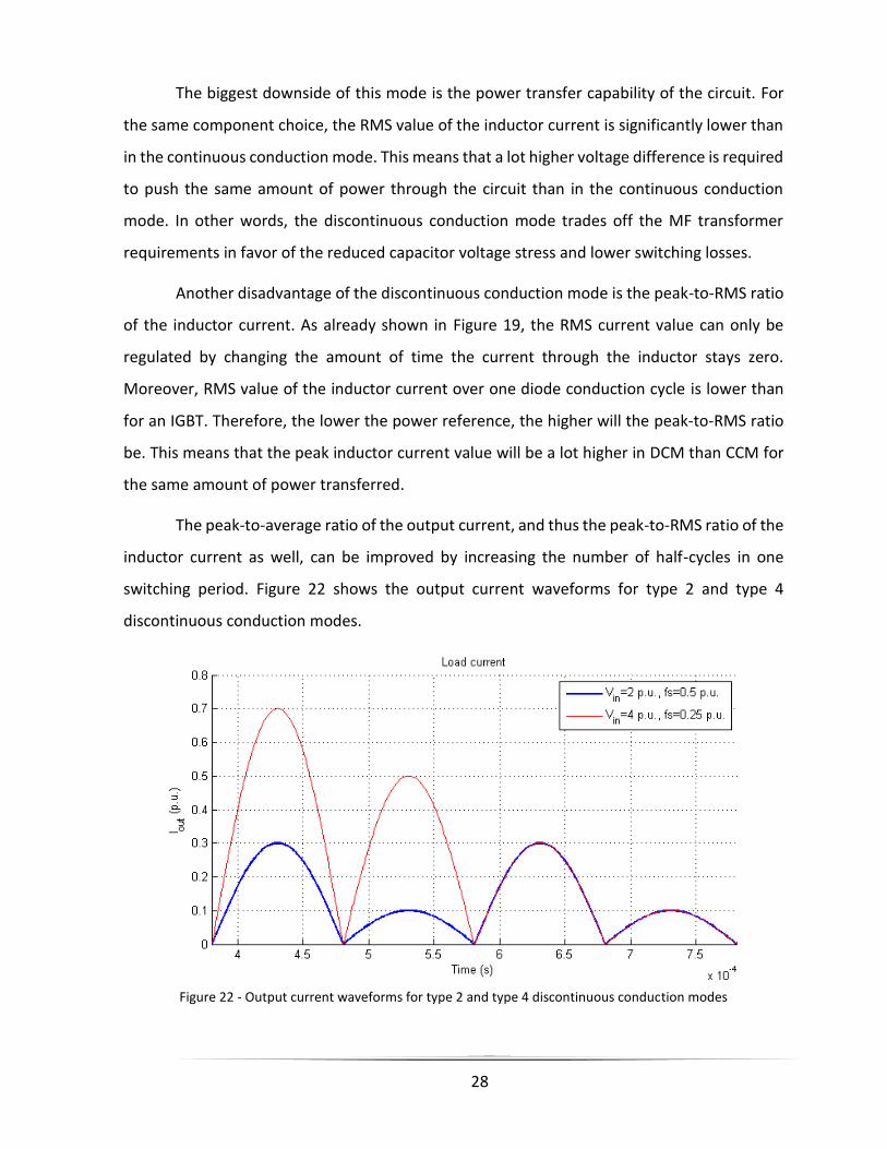
The peak-to-average ratio of the output current, and thus the peak-to-RMS ratio of the
inductor current as well, can be improved by increasing the number of half-cycles in one
switching period. Figure 22 shows the output current waveforms for type 2 and type 4
discontinuous conduction modes.
Figure 22 - Output current waveforms for type 2 and type 4 discontinuous conduction modes

29
When operating in the discontinuous mode at higher 𝑘𝑑 factors, the resonant tank
rings with a higher number of half-cycles within one half of the switching period. As visible
from Figure 22, the ratio of two adjacent current peaks increases with the number of finished
half-cycles. In other words, at the beginning of each half of the switching period, the difference
between the peak current values of the first and second half-cycles is smaller than between
the second and third and so on. This property can be written as
𝐼𝑜𝑢𝑡(𝑛)
𝐼𝑜𝑢𝑡(𝑛 + 1)<
𝐼𝑜𝑢𝑡(𝑛 + 1)
𝐼𝑜𝑢𝑡(𝑛 + 2) |
𝑛=1,2,3…𝑘𝑑−2
(31)
where 𝑛 is index of the half-cycle. During each of the half-cycles, the output current is
a sine wave of the resonant frequency with a fixed amplitude. The average current value over
one half of the switching period can be calculated using
𝐼𝑜𝑢𝑡 =2
𝑇𝑠∫ 𝑖𝑜𝑢𝑡(𝑡)𝑑𝑡
𝑇𝑠2
0
(32)
During that time, the output current rings with 𝑘𝑑 number of half-cycles which all have
the same duration. Expanding (32) gives
𝐼𝑜𝑢𝑡 =2
𝑘𝑑𝑇𝑟𝑒𝑠∑ ∫ 𝐼𝑜𝑢𝑡(𝑛) sin(
2𝜋
𝑇𝑟𝑒𝑠𝑡) 𝑑𝑡
𝑇𝑟𝑒𝑠2
0
𝑘𝑑
𝑛=1
(33)
Finally, solving (33) yields
𝐼𝑜𝑢𝑡 =2
𝜋𝑘𝑑∑ 𝐼𝑜𝑢𝑡(𝑛)
𝑘𝑑
𝑛=1
(34)
Equation (34) gives a simple way of calculating the average value of the output current
if the peaks of each half-cycle are known. The peak of the whole waveform over one half of
the switching period is the peak of the first half-cycle. The average-to-peak ratio can therefore
be expressed as
30
𝐼𝑜𝑢𝑡
𝐼𝑜𝑢𝑡
=2
𝜋𝑘𝑑∑
𝐼𝑜𝑢𝑡(𝑛)
𝐼𝑜𝑢𝑡(1)
𝑘𝑑
𝑛=1
(35)
Using the properties obtained in (31) and (35), it can be shown that
𝐼𝑜𝑢𝑡
𝐼𝑜𝑢𝑡
(𝑘𝑑1) >𝐼𝑜𝑢𝑡
𝐼𝑜𝑢𝑡
(𝑘𝑑2) | 𝑘𝑑1 > 𝑘𝑑2 (36)
This means that an increase in 𝑘𝑑 factor improves the average-to-peak ratio of the
output current.
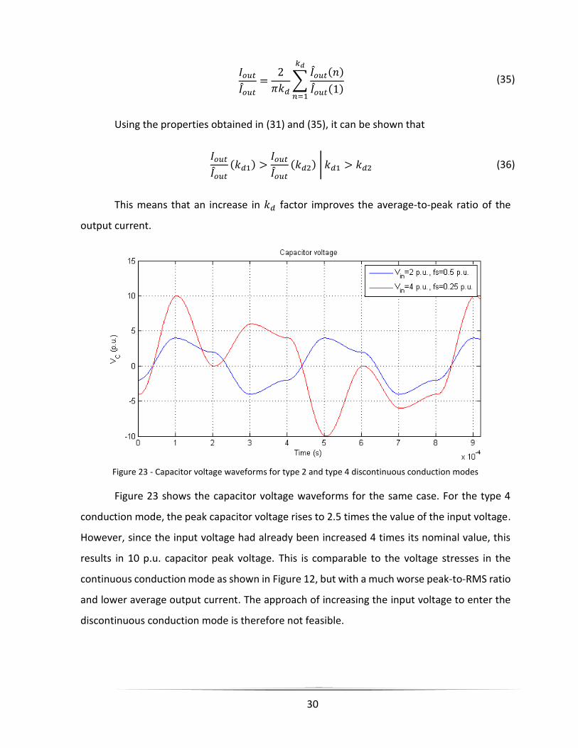
Figure 23 - Capacitor voltage waveforms for type 2 and type 4 discontinuous conduction modes
Figure 23 shows the capacitor voltage waveforms for the same case. For the type 4
conduction mode, the peak capacitor voltage rises to 2.5 times the value of the input voltage.
However, since the input voltage had already been increased 4 times its nominal value, this
results in 10 p.u. capacitor peak voltage. This is comparable to the voltage stresses in the
continuous conduction mode as shown in Figure 12, but with a much worse peak-to-RMS ratio
and lower average output current. The approach of increasing the input voltage to enter the
discontinuous conduction mode is therefore not feasible.

31
However, for this particular application, the input and output voltages levels will both
be fixed. This means that the only possibility to alter the voltage transfer ratio is by changing
the transfer ratio of the MF transformer within the converter. Increasing the number of turns
on the secondary side effectively lowers its voltage as perceived by the primary side.
Therefore, the effective DC voltage transfer ratio is given by
𝑘𝑣′ =
𝑁2
𝑁1∙
𝑉𝑖𝑛
𝑉𝑜𝑢𝑡 (37)
where 𝑁1 is the number of turns on the primary and 𝑁2 the number of turns on the
secondary side of the MF transformer. The output current waveforms for the same conduction
type modes are shown in Figure 24. The currents have been recalculated to the primary side.
Figure 24 - Output current waveforms for discontinuous conduction modes with the lower MVDC side
In comparison with Figure 22, the current waveforms stay practically the same, but
with much lower peak values. Moreover, the current gain achieved by increasing the 𝑘𝑑 factor
from 2 to 4 is significantly lower. This is a natural consequence of having a lower voltage
difference between the input and the output compared to when the input voltage was
increased.
The capacitor voltage waveforms are shown in Figure 25. The capacitor peak-to-input
voltage ratio stayed the same as before, 2 for type 2 and 2.5 for type 4 conduction modes.

32
However, since the input voltage is now lower, so is the peak voltage stress. Otherwise the
waveforms stayed the same, simply scaled by a constant.
Figure 25 – Capacitor voltage waveforms for discontinuous conduction modes with the lower MVDC side
Overall, due to the fact the increase in current does not proportionally follow the
decrease in voltage, the output power decreases with the 𝑘𝑑 factor when only the transformer
transfer ratio is altered. This is shown in Figure 26. Since 𝑘𝑑 is an integer, the curve had been
fitted with a 5th order polynomial for easier readability.
Figure 26 - Average output power dependence on discontinuous conduction mode type

33
The figure shows that, for this and similar high power transfer applications, it is almost
obligatory to use 𝑘𝑑 factor of 2. Moreover, looking at the output power values, it is visible that
they are far below the desired level. This means that a resonant tank with a much higher
characteristic admittance value has to be selected for operation in DCM compared to CCM.
Since the analysis was performed at the boundary condition of the DCM, with the
inductor current not staying at zero, Figure 26 also depicts the maximum power transfer that
can be achieved in each of the modes. Therefore, if the converter needs to operate solely in
DCM, the L and C component selection has to be made in such a way that the maximum power
transfer is achieved when it operates on the boundary between the two conduction modes.

34
4.4 Power relations
In this particular application, the resonant converter will be used to control the output
power. In order to design a controller, relations between the output power and the switching
frequency need to be obtained. The known variables are the input and output voltages,
transformer turns ratio and resonant tank’s inductance and capacitance values. The circuit is
still assumed to be ideal.
As stated before, in the continuous conduction mode, the capacitor and the inductor
waveforms can be approximated by ideal sinusoidals. Starting from the result obtained in (25)
and including the transformer turns ratio, the average output power can be written as
𝑃𝑜𝑢𝑡 =2√2
𝜋
𝑁1
𝑁2𝑉𝑜𝑢𝑡 ∙ √𝑉𝑖𝑛
2 − (𝑁1
𝑁2𝑉𝑜𝑢𝑡
)2
∙ |2𝜋𝑓𝑠𝐶
1 − 4𝜋2𝑓𝑠2𝐿𝐶
| (38)
The equation can be simplified by recalculating the output voltage to the transformer’s
primary side as
𝑉𝑜𝑢𝑡′ =
𝑁1
𝑁2𝑉𝑜𝑢𝑡 (39)
Then, solving (38) for 𝑓𝑠 gives
𝑓𝑠 =|
| 𝑉𝑜𝑢𝑡
′
𝐶√𝑉𝑖𝑛2 − 𝑉′𝑜𝑢𝑡
2 ± √𝐶2(𝑉𝑖𝑛
2 − 𝑉′𝑜𝑢𝑡2
) + √2𝜋𝐿𝐶 (𝑃𝑜𝑢𝑡
𝑉𝑜𝑢𝑡′ )
2
√2𝜋2𝐿𝐶𝑃𝑜𝑢𝑡
|
| (40)
Equation (40) gives an explicit relationship between the desired power output and the
switching frequency when the converter operates near the resonance region and can be used
for feed-forward control of the converter. If the sign is negative, the converter will operate in
the sub-resonance region, while for the positive, in the super-resonance region.
35
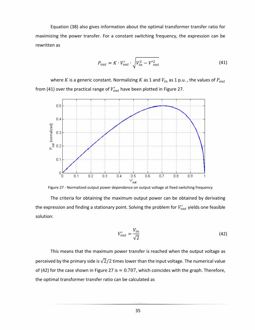
Equation (38) also gives information about the optimal transformer transfer ratio for
maximizing the power transfer. For a constant switching frequency, the expression can be
rewritten as
𝑃𝑜𝑢𝑡 = 𝐾 ∙ 𝑉𝑜𝑢𝑡′ ∙ √𝑉𝑖𝑛
2 − 𝑉′𝑜𝑢𝑡2 (41)
where 𝐾 is a generic constant. Normalizing 𝐾 as 1 and 𝑉𝑖𝑛 as 1 p.u. , the values of 𝑃𝑜𝑢𝑡
from (41) over the practical range of 𝑉𝑜𝑢𝑡′ have been plotted in Figure 27.
Figure 27 - Normalized output power dependence on output voltage at fixed switching frequency
The criteria for obtaining the maximum output power can be obtained by derivating
the expression and finding a stationary point. Solving the problem for 𝑉𝑜𝑢𝑡′ yields one feasible
solution:
𝑉𝑜𝑢𝑡′ =
𝑉𝑖𝑛
√2 (42)
This means that the maximum power transfer is reached when the output voltage as
perceived by the primary side is √2/2 times lower than the input voltage. The numerical value
of (42) for the case shown in Figure 27 is ≈ 0.707, which coincides with the graph. Therefore,
the optimal transformer transfer ratio can be calculated as

36
𝑁1
𝑁2=
𝑉𝑖𝑛
√2 𝑉𝑜𝑢𝑡
(43)
For the discontinuous conduction mode, the resonant tank does not have a sinusoidal
response anymore and therefore (40) cannot be applied. The power equation can be derived
from the responses shown in Figure 28. This is done for the 𝑘𝑑 factor of 2.
Figure 28 - Inductor current and capacitor voltage responses for deriving the power equation
From the moment the antiparallel diode start conducting until the transistor turns off
naturally, a positive charge, represented by the area under the orange curve, flows into the
capacitor. During that period, the capacitor voltage changes from −2𝑉𝑖𝑛 to +2𝑉𝑖𝑛. Knowing
the capacitance value, the area under the curve can be calculated as
𝑄 = 4 ∙ 𝐶 ∙ 𝑉𝑖𝑛 (44)
During the same period, the average inductor current is equal to
⟨𝑖𝐿(𝑡)⟩𝑇𝑠= 2 ∙ 𝑄 ∙ 𝑓𝑠 (45)
The same current, scaled by the transformer’s transfer ratio, flows through the passive
rectifier on the secondary side of the transformer. The passive rectifier supplies the load with

37
the current of the same magnitude and a positive sign. This means that the scaled average
output current is the same as the average inductor current given by (45). If the transformer is
ideal, the power on its primary side is the same as the power on its secondary. Therefore, an
expression linking the average output power to the switching frequency can be obtained by
combining (39), (44) and (45) as
𝑃𝑜𝑢𝑡 = 8 ∙ 𝐶 ∙ 𝑉𝑖𝑛 ∙ 𝑉𝑜𝑢𝑡′ ∙ 𝑓𝑠 (46)
Comparing (40) and (46), it is clear that controlling the power is much simpler in the
discontinuous conduction mode. The latter expression also indicates that the output power is
proportional to the output voltage, which, under the limitation of (28), means that the
maximum power transfer is achieved when
𝑁1
𝑁2=
𝑉𝑖𝑛
2 𝑉𝑜𝑢𝑡 (47)
Moreover, since the switching frequency is limited, the maximum power transfer that
can be achieved in the discontinuous conduction mode can be calculated using (4), (46) and
(47), which yields
𝑃𝑜𝑢𝑡,𝑚𝑎𝑥 =𝑉𝑖𝑛
2
𝜋√
𝐶
𝐿 (48)
This means that the output power is proportional to the characteristic admittance of
the resonant tank. Equation (48) is very useful for dimensioning the resonant tank components
when the output power requirement is known.

38
4.5 Loss estimation
Since the converter will be used for high power applications, it is important to be able
to accurately estimate its losses. The calculated losses can afterwards be used for estimating
the working temperature of the converter and dimensioning the cooling system. They can also
be used for evaluating the overall conversion efficiency and thus assessing the financial
feasibility of such a solution. The total power loss will be distributed over the 4 main
components – the IGBT bridge, the resonant tank, the MF transformer and the passive
rectifier.
The total IGBT bridge loss can be calculated as a combination of transistor losses and
diode losses. These can furthermore be divided into two categories – the conduction losses
and the switching losses. For the conduction losses calculation, the IGBT can be approximated
by a series connection of a resistor, representing the on-state collector-emitter resistance, and
a voltage source, representing the on-state zero-current collector-emitter voltage [4]. The
analogous approximation can be applied to the anti-parallel diode, giving
𝑢𝐶𝐸 = 𝑢𝐶𝐸0 + 𝑟𝐶𝐸𝑖𝐶 (49)
𝑢𝐷 = 𝑢𝐷0 + 𝑟𝐷𝑖𝐷 (50)
The instantaneous power loss can therefore be calculated as a product of voltage and
current. The average conduction losses over one switching period can be calculated as
𝑃𝐶𝑇 =1
𝑇𝑠∫ [𝑢𝐶𝐸0𝑖𝐶(𝑡) + 𝑟𝐶𝐸𝑖𝐶
2(𝑡)]
𝑇𝑠
0
𝑑𝑡 (51)
𝑃𝐶𝐷 =1
𝑇𝑠∫[𝑢𝐷0𝑖𝐷(𝑡) + 𝑟𝐷𝑖𝐷
2 (𝑡)]
𝑇𝑠
0
𝑑𝑡 (52)
Solving (51) and (52) gives

39
𝑃𝐶𝑇 = 𝑢𝐶𝐸0 𝐼𝐶,𝑎𝑣𝑔 + 𝑟𝐶𝐸 𝐼𝐶,𝑟𝑚𝑠2 (53)
𝑃𝐶𝐷 = 𝑢𝐷0 𝐼𝐷,𝑎𝑣𝑔 + 𝑟𝐷 𝐼𝐷,𝑟𝑚𝑠2 (54)
Conduction losses in the off-state on the other hand can be neglected due to very low
leakage current values.
The switching losses are typically very demanding to calculate analytically [5], [6] and
require numerous parameters of which some often cannot be found in the manufacturer’s
datasheets. Another approach is to use computer simulation tools to calculate the switching
losses. However, since the switching transients occur at the level of nanoseconds, a very small
time step is required to solve such systems and the models still require a great number of
parameters.
The simulation tool used is Plecs, which simulates electrical circuits on a system level.
To solve them at high speed, all the switching devices are modelled as ideal switches, meaning
that the current and voltage changes are instantaneous. The switching losses will therefore be
estimated by capturing the current and voltage values at the switching instances and using the
lookup tables provided by device manufacturers to determine the energy loss at each instant.
The same methods as the ones described above can be used to calculate the rectifier
losses.
The resonant tank will generate losses due to series resistance of an inductor and a
capacitor. The average power loss can be calculated as
𝑃𝑡𝑎𝑛𝑘 = (𝑅𝐿 + 𝑅𝐶) 𝐼𝐿,𝑟𝑚𝑠2 (55)
The transformer losses can be divided into two categories – core losses and copper
losses. Core losses consist of hysteresis and eddy current losses. These losses can be very
accurately estimated in the conventional transformers excited by 50/60 Hz sine waves.
However, since the MF transformers are normally excited by rectangular waveforms and at
much higher frequencies, the loss estimation gets a lot more complicated [7], [8].

40
The hysteresis losses are proportional to the frequency, while the eddy current losses
to the frequency squared. The fact that resonant converters operate by altering the switching
frequency makes the analysis even more complicated. The equivalent electrical scheme of the
transformer would need to use variable inductances and resistances to compensate for the
change in the excitation frequency.
The MF transformers have a much higher ratio of core losses in the overall losses due
to significantly higher frequencies they operate in. However, thanks to the new materials used
in MF transformer’s core and windings, their overall losses are comparable to the ones of
conventional transformers [9], with efficiencies exceeding 99%. Therefore, the transformer
core losses will be neglected. Since the resonant tank’s inductor is often integrated in the
transformer, the conduction losses of the resonant tank will include the transformer
conduction losses in this simulation.

41
Most important points stated in this chapter are the following:
Series-resonant converter circuit can be modelled using 3 linear circuits if the
switching frequency is close to the resonant frequency
Input voltage always has to be higher than the output voltage scaled by the
transformer’s transfer ratio, otherwise no power can be transferred
Component stress increases significantly as the switching frequency
approaches the resonant frequency
Capacitor voltage is independent of the choice of L and C values, which makes
it possible to design a resonant tank based on the maximum permissible
capacitor voltage and output power requirements
As a general rule, the lower the inductance and higher the capacitance, the
greater the amount of power that can be transferred through the circuit
Addition of dead time to the control signal does not influence the circuit’s
performance as long as the duty cycle remains above 85%
Two biggest advantages of DCM compared to CCM are zero current switching
and limited capacitor voltage
Increasing the number of conduction half-cycles in DCM improves the peak-to-
average ratio of the output current, but increases the peak capacitor voltage
and reduces the amount of power that can be transferred through the circuit
A lot higher characteristic admittance of resonant tank components is required
to transfer the same amount of power in DCM compared to CCM
The choice of transformer’s transfer ratio influences the amount of power that
can be transferred through the circuit and its optimal value is different for CCM
and DCM
Relationship between the output power and switching frequency is linear in
DCM while highly nonlinear in CCM. This means that DCM converters require a
substantially simpler control system

42
5 Resonant converter design
5.1 Component selection
This section proposes a 10 MW circuit configuration. The necessary input parameters
are voltage levels and output power. Wind turbine generators are normally rated at 690 V.
However, since the subject of this analysis is a 10 MW wind turbine, an assumption will be
made that a 3.3 kV generator is used to reduce the current rating of the components. Another
assumption is that the turbine uses a passive rectifier with a large DC link capacitor at its
output. This means that the converter input voltage will be equal to the peak value the rated
generator voltage, giving
𝑉𝐿𝑉𝐷𝐶 = √2 ∙ 3300 𝑉 ≈ 4667 𝑉 (56)
At the same time, the MVDC voltage level will be rated at 35 kV. The chosen switching
frequency is 5000 kHz.
Based on previous observations, a DC-DC resonant converter circuit can be designed.
Due to reduced switching losses and lower component voltage stress, discontinuous
conduction mode has been chosen for the whole operating range. In accordance with the
conclusions made in the previous section, 𝑘𝑑 factor of 2 has been selected. Assuming the input
and output voltages will not change more than ± 10% in normal operation, the transformer
transfer ratio can be calculated using (47) as
𝑁2
𝑁1=
2 ∙ 1.1 ∙ 𝑉𝑀𝑉𝐷𝐶
0.9 ∙ 𝑉𝐿𝑉𝐷𝐶≈ 19 (57)
The transfer ratio calculated in (57) has been rounded up to the nearest integer to
ensure the converter stays in type 2 DCM. Having the transformer transfer ratio selected, the
required resonance tank’s capacitance can be calculated using (46). Since the converter should
be able to operate in DCM at all times, this gives

43
𝐶 =𝑃𝑜𝑢𝑡
4 ∙ 𝑓𝑟𝑒𝑠 ∙ 0.92 ∙ 𝑉𝐿𝑉𝐷𝐶 ∙ 𝑉𝑀𝑉𝐷𝐶′ = 71.8 𝜇𝐹 (58)
The inductance value can be obtained from (4) as
𝐿 =1
4𝜋2𝑓𝑟𝑒𝑠 2 𝐶
= 14.1 𝜇𝐻 (59)
The resonant tank components need to be designed to withstand the peak voltage and
current stresses. The peak capacitor voltage stress is given by (30), which yields
𝑣𝐶 = 2 ∙ 𝑉𝐿𝑉𝐷𝐶 = 9334 𝑉 (60)
The peak current stress is difficult to calculate and therefore has been obtained by
simulation, which yielded 14.8 kA. The result indicates that it would be beneficial to split the
converter circuit into several identical parallel modules. The benefits of doing so are reduced
component current ratings, reduced conduction losses and increased redundancy. On the
other hand, this will make the control system more complex.
Splitting resonant converters into modules cannot be done by simply taking several
previously designed modules and connecting them in parallel. The reason for that is given by
Figure 28. The basic principle of controlling the average output power in DCM is by changing
the switching frequency and therefore creating a longer time period over which the power will
be averaged. This is also given by equation (46). However, the peak current value will remain
the same as it depends on the amount of charge stored in the capacitor, which is in return
proportional to the input voltage. Therefore, connecting the modules in parallel would not
reduce their peak current value, but simply the time between two peak instances.
To split the resonant converter into several modules, their capacitance and inductance
values need to be scaled. If the converter should to be split into 𝑛𝑚 modules, the capacitance
and inductance values of each module can be calculated from the earlier obtained values as

44
𝐶𝑚𝑜𝑑 =𝐶
𝑛𝑚 (61)
𝐿𝑚𝑜𝑑 = 𝐿 ∙ 𝑛𝑚 (62)
This solution will propose splitting a converter into 4 modules, which means that each
module will have a power rating of 2.5 MW. The new capacitance and inductance values are
therefore
𝐶𝑚𝑜𝑑 = 17.95 𝜇𝐹 (63)
𝐿𝑚𝑜𝑑 = 56.4 𝜇𝐻 (64)
Using these values, peak current was brought down to 3.7 kA, which coincides with the
expected results. The frequency characteristic of the converter did not change, meaning that
the nominal operating point remained the same.
Finally, it is useful to know the peak energy stored in the components for their
dimensioning. The peak capacitor and inductor energy per module can be calculated using
𝐸𝐶,𝑚𝑜𝑑 = 𝐶𝑚𝑜𝑑 ∙𝑣𝐶
2
2= 782 𝐽 (65)
𝐸𝐿,𝑚𝑜𝑑 = 𝐿𝑚𝑜𝑑 ∙𝑖𝐿
2
2= 386 𝐽 (66)
The results show that, since resonant converters operate at high frequencies, the peak
energy stored in each of the resonant tank components is relatively low compared to the
power rating of the circuit. This is one of the factors that can lead to a reduction in size and
weight.

45
5.2 Control system
The proposed control system diagram is shown in Figure 29.
Figure 29 - Control system layout
The input parameters are the power reference, input and output voltage
measurements and the output current measurement. These 3 quantities provide base inputs
for the control system, which is implemented as a combination of a feed-forward and a
feedback controller. All the measurements need to be averaged over one switching period,
but since the switching frequency changes during operation, variable time sampling needs to
be used. The switching frequency is therefore fed back to the time average block, which uses
it to determine the length of the averaging period. The averaging period is updated only once
the previous one is over, meaning that intermediate changes in the frequency reference
imposed by the PI controller do not have an impact on its value. The same rule applies for the
pulse generator. The pulse frequency is updated only once the previous switching period
finishes, as updating the switching frequency continuously would create jitter, harmonics and
DC offset in the converter output voltage, rendering the circuit unstable.
The feed-forward controller implements the control law given by (46). Since the
equation was derived from an idealized circuit, the imperfections such as the switch on-
resistance or the resonant tank’s series resistance will cause some losses and therefore the
actual power output will be lower than calculated. The purpose of the PI controller is to adjust
the frequency reference to compensate for the difference between the idealized model and
the real circuit.

46
It is possible that, due to some unpredictable events, such as voltage fluctuations
exceeding the 10% tolerance level for example, the converter cannot temporarily deliver the
desired amount of power while operating in the discontinuous conduction mode. The control
will respond on two levels.
First, if the cause for such a behavior is due to a voltage drop in the input or an increase
in the output voltage of an unexpected magnitude, the feed-forward controller will give out a
new power reference which will be above the half of the resonant frequency. This will cause
the circuit to enter the continuous conduction mode, thus making the power relation (46)
invalid. However, as shown in Figure 19 and Figure 21, at these frequencies the current and
voltage responses are still highly non-sinusoidal, meaning that the power relation for the
continuous conduction mode given by (40) cannot be used either. At the same time, the
current and voltage waveforms resemble the discontinuous conduction waveforms a lot closer
than the ones of near-resonant operation, meaning that the difference between the calculated
and the actual output power will be relatively small. This is shown in Figure 30 on the example
of a proposed 2.5 MW module. The difference gets bigger as the frequency increases, but since
the switching frequency should not drift far away from 2500 Hz, the error will stay small and
be easily handled by the PI controller.
Figure 30 - Actual and calculated output power dependence on switching frequency

47
Second, regardless of the cause of the disturbance, the PI controller will register a
difference between the actual power and its reference and increase the switching frequency.
However, since entering the continuous conduction mode will also lead to increased voltage
and current stress of the components, it is also important to monitor their values and
implement protection mechanisms.
A two-level protection scheme with both soft and hard stop is proposed. Since circuit
protection is only marginally covered by the scope of this project, an example will be given on
inductor protection. The protection system schematic is shown in Figure 31.
Figure 31 - Inductor protection mechanism
The protection system is connected between the frequency reference summation
point and the pulse generator from Figure 29. The monitored quantities are the inductor
current and temperature. The inductor might or might not be integrated in the transformer.
During normal operation, the inductor protection block acts as a direct feed through for the
frequency reference. In case the circuit goes into temporary and permissible overload, the soft
stop mechanism adjusts the frequency reference to keep the inductor temperature within
permissible limits. Since the inductor’s thermal constant is a lot higher than the electrical, this
means that the switching frequency will stay intact at first once it enters the soft stop zone,
but as time passes, the increase in the inductor temperature will cause the protection system
to decrease the switching frequency more and more, until either the temporary event passes

48
and the converter returns to normal operating state, or hard stop protection gets triggered.
Hard stop protection monitors if the measured quantities are below their highest permissible
values. In case the overload lasts for too long and the inductor temperature increases too
much, or an abrupt load voltage drop causes the inductor current to grow very fast above its
nominal value, hard stop protection will trip and switch the converter off instantaneously.
While the converter is in off state, no energy is stored in its components. This means
that the capacitor voltage and inductor current are equal to zero. Once the converter gets
turned on, it takes several cycles to reach the steady-state operating point. The transient
response of the converter contains overshoots due to balancing of energy storage elements.
As the controller response time between two consecutive reference adjustments is one
switching period, these transients cannot be controlled as they appear at the resonant
frequency. Current and voltage overshoots would most likely trip hard-stop protection
mechanisms, turning the converter off before it even started up.
Figure 32 - Capacitor voltage and inductor current waveforms during startup (full line) and steady state (dotted)
This problem can, however, be solved using a capacitor pre-charge mechanism. As
stated before, current and voltage overshoots occur due to a difference between the amount
of energy stored in the capacitor and the inductor in steady-state and at the moment of

49
starting the converter up, when they are both assumed to be zero. Observing Figure 32, it is
clear that, within one switching period, the inductor current crosses zero four times. Since the
inductor current is also zero when the converter is off, pre-charging the capacitor to either
one of these voltage values would create the same conditions as if the converter was already
in steady state, thus completely eliminating the overshoot. Four possible solutions have been
obtained by simulation.
𝑣𝐶0−1,2 = ±9320 𝑉 (67)
𝑣𝐶0−3,4 = ±3675 𝑉 (68)
The amplitude of the first two solutions corresponds to approximately twice the input
voltage, which had already been discussed in section 4.3. The small difference is caused by an
added 1 mΩ resistor in order for the simulation to converge. The second solution pair is
however more interesting, as the voltage amplitude is lower than the input voltage. Assuming
the capacitor will be charged from the input source and not an external power supply, charging
the capacitor to twice the input voltage would require an extra DC/DC converter to boost the
voltage up. On the other hand, charging the capacitor to a lower voltage level than the input
can be done with the addition of a simple resistor to limit the charging current. The proposed
capacitor pre-charge solution is shown in Figure 33.
Figure 33 - Resonant converter circuit with a capacitor pre-charge mechanism
In case it is desired that the inductor current starts positive at the beginning of the first
switching period, the capacitor should be pre-charged to -3675 V. The charging starts by

50
closing the switch, at which point a simple series RC circuit is formed. The capacitor voltage in
this situation can be described by a well-known formula as
𝑣𝐶 (𝑡) = −𝑉𝐿𝑉𝐷𝐶(1 − 𝑒
−𝑡
𝑅𝑐ℎ𝐶) (69)
Increasing the charge resistor’s magnitude increases the time constant of the circuit,
which is in this case given by
𝜏 = 𝑅𝑐ℎ𝐶 (70)
The higher the time constant, the slower will the circuit respond and therefore the
lower will the charging current be. By adjusting the resistance value, it is possible to determine
at which time instant the capacitor voltage will reach (68) and thus when the charging circuit
should disconnect. This can be calculated using
𝑡𝐶0 = −𝑅𝑐ℎ𝐶 ∙ ln (𝑣𝐶0
𝑉𝐿𝑉𝐷𝐶+ 1) (71)
The maximum charging current can be obtained from (69), which yields
𝑖𝑐ℎ,𝑚𝑎𝑥 =𝑉𝐿𝑉𝐷𝐶
𝑅𝑐ℎ (72)
For the values of 𝐶 = 17.95 𝜇𝐹, 𝑣𝐶0 = −3675 𝑉 and 𝑅𝑐ℎ = 100 Ω, this results in
𝑡𝐶0 = 2.8 𝑚𝑠 (73)
𝑖𝑐ℎ,𝑚𝑎𝑥 = 46.7 𝐴 (74)
The obtained time to charge is significantly higher than the controller response time,
while the peak charge current is significantly lower than the peak current during normal
operation. This means that the pre-charge mechanism does not introduce any additional
requirements on the rest of the circuit and therefore provides a very cost-effective solution of
eliminating the overshoot during startup operation.

51
Figure 34 - Capacitor and input voltage and output current waveforms during a converter startup with a pre-
charge mechanism
The converter startup sequence with the capacitor pre-charge circuit is shown in Figure
34. The converter starts operating at full power as soon as the charge circuit disconnects. As
visible from the simulation results, the overshoot has been completely eliminated.

52
Most important points stated in this chapter are the following:
Despite using a generator with significantly higher voltage rating than it is usual
in conventional wind turbines, very high peak currents will likely require the
converter to be split into several modules
When splitting series-resonant converters into modules, resonant tank
parameters need to be recalculated depending on the number of modules
used. This does not change the converter’s resonant frequency
Since resonant converters operate at much higher frequencies than
conventional converters, the amount of energy they store is significantly lower,
which allows a reduction in their size and weight
Feed-forward controller can be tuned using ideal circuit’s parameters, while a
feedback controller can be used to compensate for the difference between the
ideal and real circuit
The converter can temporarily operate in CCM in case the situation requires it,
but the components should be monitored for overload
Current and voltage overshoot during startup can be eliminated using a simple
capacitor pre-charge circuit

53
6 Model validation
6.1 Laboratory setup
Laboratory setup schematic is shown in Figure 35. The main converter circuit consists
of a 40 V voltage source, 68 µF DC link capacitors, full IGBT bridge, air-core inductor, resonant
tank capacitor bank, MF transformer, full bridge rectifier and an active 40 V load. Auxiliary
components include two gate driver circuits with their own multi-channel 0-30V/5V power
supply, a signal generator and a scope with voltage and current probes.
Figure 35 - Laboratory setup schematic
Nearly all of the setup components had to be built from parts. The medium frequency
transformer, shown in Figure 36, was made using 4 E-shaped N87 silicon-ferrite half-cores, a
coil former and wounded by hand using laminated copper wire. Primary and secondary
windings were insulated using Mylar foil. Using the RLC meter, transformer’s magnetization
and leakage inductances, as well as winding resistances were obtained. The measurements
were made at 10 kHz to ensure that skin effect and core nonlinearities occurring at higher
frequencies are taken into account. Since the T/2 equivalent scheme was used for the
simulation, the resistance and leakage inductance are given as lumped values transferred to
the primary side. For practical reasons, the measured values for all the components are given
in a single table at the end of this section.
54
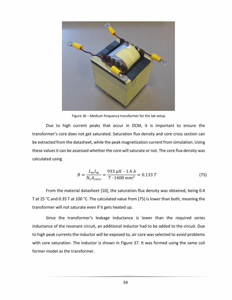
Figure 36 – Medium frequency transformer for the lab setup
Due to high current peaks that occur in DCM, it is important to ensure the
transformer’s core does not get saturated. Saturation flux density and core cross section can
be extracted from the datasheet, while the peak magnetization current from simulation. Using
these values it can be assessed whether the core will saturate or not. The core flux density was
calculated using
𝐵 =𝐿𝑚𝐼𝑚
𝑁1𝐴𝑐𝑜𝑟𝑒=
933 𝜇𝐻 ∙ 1.4 𝐴
7 ∙ 1408 𝑚𝑚2= 0.133 𝑇 (75)
From the material datasheet [10], the saturation flux density was obtained, being 0.4
T at 25 °C and 0.35 T at 100 °C. The calculated value from (75) is lower than both, meaning the
transformer will not saturate even if it gets heated up.
Since the transformer’s leakage inductance is lower than the required series
inductance of the resonant circuit, an additional inductor had to be added to the circuit. Due
to high peak currents the inductor will be exposed to, air core was selected to avoid problems
with core saturation. The inductor is shown in Figure 37. It was formed using the same coil
former model as the transformer.

55
Figure 37 - Resonant tank inductor for the lab setup
The IGBT bridge is shown in Figure 38. It consists of four 1200 V/40 A IGBT’s without
antiparallel diodes, which were added later to the setup. The components were placed on a
heat sink to enhance heat dissipation. To avoid generating parasitic inductance that would
alter the frequency characteristic of the circuit, flat copper busbars were used to connect the
components together. To prevent accidental short circuits or touching live conductors, most
of the busbars were insulated with the insulation removed only at the points where contacts
were soldered.

56
Figure 38 - IGBT bridge for the lab setup
The IGBT bridge was driven by a pair of single-input, isolated high/low side gate drivers.
Each driver had an integrated dead time and overlap protection, giving mutually inverse pulses
to both the high and low side transistors within one converter leg. This is more closely shown
in Figure 39. The other converter leg used the same gate driver model, but with high and low
side gate pulses inverted. This configuration made controlling the full bridge converter using
only a single signal generator possible. The complete driver circuit configuration was
implemented on a stripboard, together with capacitors for stabilizing the terminal supply
voltages, dead time control resistor and a bootstrap circuit.

57
Figure 39 - Internal gate driver module configuration [11]
Gate driver circuit test is shown in Figure 40. Control signal comes from the signal
generator and has an amplitude between 0 - 5 V. Output side of the gate driver is supplied
from a 15 V source, which is also the voltage used to turn the transistors on. The top and
bottom gate signals are mutually inverse and stable, which validates the circuit operation.
Figure 40 - Gate driver circuit test: gate control signal (1), bottom gate voltage (2), top gate voltage (3)
To avoid short circuiting the input voltage source, dead time had to be implemented
to make sure one transistor has enough time to turn off before the other one turns on. From
the device datasheet [12] it was obtained that the highest switching time occurs at a turn-off

58
at zero current and equals 800 ns. Dead time was programmed by connecting a resistor
between the gate driver’s DT pin and the supply voltage ground and its magnitude had been
selected to give dead time of 1 µs. Dead time test is shown in Figure 41, which confirms it had
been programmed correctly.
Figure 41 - Dead time test: gate control signal (1), bottom gate voltage (2), top gate voltage (3)
As shown earlier, dead time can in some cases seriously influence the converter
circuit’s performance. In this particular case, the highest frequency IGBTs would operate at
during normal operation is half of the resonant frequency, giving a time period of 162 µs. This
results in duty cycle of the gate signal of 99.3 %, which should not have any unwanted impacts
on the circuit’s performance according to the findings of section 4.2.5.
The rectifier bridge is shown in Figure 42. As the IGBT converter, it was also attached
to a heat sink and connected using insulated copper busbars. It consists of four 300 V/2x15 A
fast recovery diodes. Since the anodes have been shorted, the maximum current each device
can withstand is 30 A.

59
Figure 42 - Diode rectifier bridge for the lab setup
The transformer and resonant tank parameters are given in Table 2. The same
parameters were used in the loss estimation simulation.
Table 2 – Transformer and resonant tank parameters measured at 10 kHz
Parameter Description Value
𝑳𝒎 Transformer magnetization inductance 933 µH
𝑳𝒍 Transformer leakage inductance 8.7 µH
𝑹𝑻 Transformer winding resistance 238 mΩ
𝑵𝟏 Number of turns on the primary 7
𝑵𝟐 Number of turns on the secondary 18
𝑳 Air core inductor’s inductance 19.1 µH
𝑹𝑳 Air core inductor’s series resistance 100 mΩ
𝑪 Resonant tank capacitor’s capacitance 6 µF
𝑹𝒄 Resonant tank capacitor’s series resistance 108 mΩ

60
Having all of the key circuit parameters measured, it is possible to finalize the design
and give the preliminary converter specification in Table 3.
Table 3 - Preliminary converter specification for the lab setup
Parameter Value
Power rating 150 W
Nominal input voltage 40 V
Input voltage tolerance ± 10%
Nominal output voltage 40 V
Output voltage tolerance ± 10%
Resonant frequency 12.32 kHz
The power rating was calculated using (46). Since this power relation was derived for a
lossless circuit, the actual maximum power output achievable within the given voltage limits
while staying in DCM is lower. This means that, in case both the output and input voltages
drop 10% from their nominal value at the same time, the converter will have to enter CCM to
continue delivering 150 W at its output.

61
6.2 Simulation results
The laboratory circuit was modelled in Plecs and used to estimate conduction and
switching losses. I-V curves for calculating the conduction losses of semiconductor devices
were obtained from the component datasheets [12], [13], [14], together with E-I curves for
the IGBT turn-on and turn-off power loss estimation. The rectifier diode datasheet did not
contain such a table, so the switching losses in the passive rectifier were neglected. However,
since turn-offs and turn-ons always occur at zero current, it is safe to assume the majority of
losses associated with the rectifier will be caused by conduction rather than switching.
The losses were evaluated at different operating points. Figure 14 shows how the
losses change with the output power. The output power was varied from 10 to 110% of its
nominal value, while the input and output voltages were kept constant at 40 V. Due to the fact
all the switching occurs at zero current, the estimated switching losses were below 20 mW and
therefore omitted from the figure.
Figure 43 - Power loss dependence on output power at nominal voltage level
Two important things are visible from the graph. First, the relationship between the
power loss and the output power is linear within the whole operating range, even though it
has been shown in (53)-(55) that the conduction losses in semiconductors are nonlinear, while
the conduction losses in copper are proportional to the current squared. This is due to the fact
the converter can deliver 110% of output power at nominal voltage while remaining in DCM.

62
As discussed earlier, current and voltage waveforms in DCM stay the same while the converter
is conducting, resulting in the same amount of energy transferred each switching period. Since
the peak, average and RMS current values do not change over the conducting part of the
switching period, the conduction losses they generate also stay the same. On the other hand,
since there is no conduction during the remainder of the switching period, there are no
conduction losses either. Maintaining constant efficiency over the full operating range is
therefore an inherent property of DCM resonant converters. This is not the case with
converters operating in CCM where the current amplitude changes together with the power
reference.
The second visible property is very poor efficiency of only 64% due to excessively high
copper losses. One of the reasons for that is an additional inductor wounded to increase the
transformer’s leakage inductance, increasing the wire length and thus series resistance of the
circuit. Another reason is that the transformer and air-core inductor were, due to lack of
materials in the lab, wounded using solid copper wire. At the current frequency of 12.32 kHz,
this lead to an increase of 21% in the effective AC resistance due to skin effect compared to
wire’s DC resistance. This means that copper losses would have been 17.4% lower if stranded
wire was used to wind the transformer and the inductor. Further improvements could be
achieved by using conductors specially designed for higher frequencies, such as Litz wire.
Figure 44 shows how the total losses change for different input and output voltages.
The worst operating point is located at the maximum input and minimum output voltage. This
is caused by the fact the highest DC voltage ratio also results in highest peak current, which in
return causes the highest conduction losses. On the other hand, the operating point with the
lowest losses is located at the lowest DC voltage ratio. At this point the circuit is operating in
CCM, which leads to a reduction of peak-to-RMS current ratio and in this case, peak current
value in general, reducing the conduction losses.
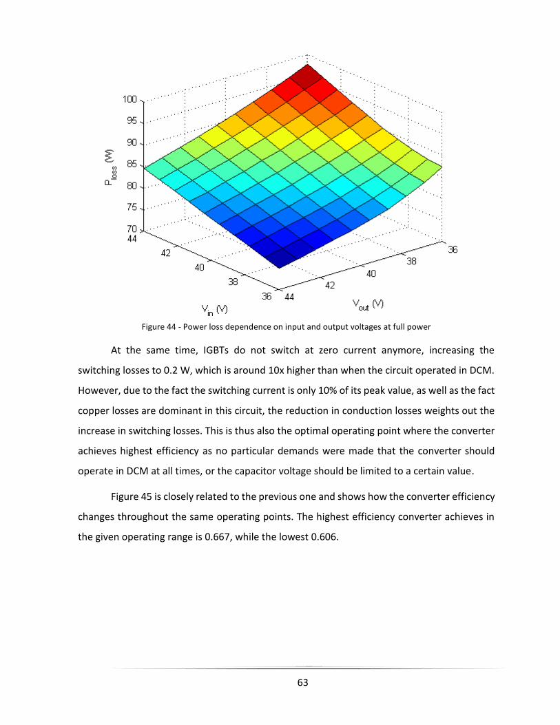
63
Figure 44 - Power loss dependence on input and output voltages at full power
At the same time, IGBTs do not switch at zero current anymore, increasing the
switching losses to 0.2 W, which is around 10x higher than when the circuit operated in DCM.
However, due to the fact the switching current is only 10% of its peak value, as well as the fact
copper losses are dominant in this circuit, the reduction in conduction losses weights out the
increase in switching losses. This is thus also the optimal operating point where the converter
achieves highest efficiency as no particular demands were made that the converter should
operate in DCM at all times, or the capacitor voltage should be limited to a certain value.
Figure 45 is closely related to the previous one and shows how the converter efficiency
changes throughout the same operating points. The highest efficiency converter achieves in
the given operating range is 0.667, while the lowest 0.606.

64
Figure 45 - Efficiency dependence on input and output voltages at full power
The simulation results show that, for small-size, low-power converters, the design
should be oriented towards reducing the conduction losses, meaning that the converters
should operate in CCM. Thin conductors lead to high characteristic resistance of the circuit,
which is even more emphasized in this particular case since the skin effect had not been taken
care of. Moreover, due to relatively low current and voltage levels used, it is fairly easy and
cheap to acquire oversized components and therefore minimize the risk of their overload. This
rendered another beneficial property of DCM – relatively low capacitor voltage – useless.
On the other hand, for high power circuits, including the 10 MW proposal made, it
might be completely infeasible to allow the peak capacitor voltage to become several dozens
of times higher than the already high input voltage. High currents on the other hand not only
impose limitations on transistors in the form of maximum current they can switch at, but also
significantly increase the switching losses. On the other hand, increase in dimensions typically
reduces the circuit’s resistance and consequently characteristic conduction losses. This means
that, at high power, the switching losses might constitute a dominant portion of the circuit’s
losses, therefore making DCM a much more feasible solution, both from the efficiency and
component rating viewpoint.
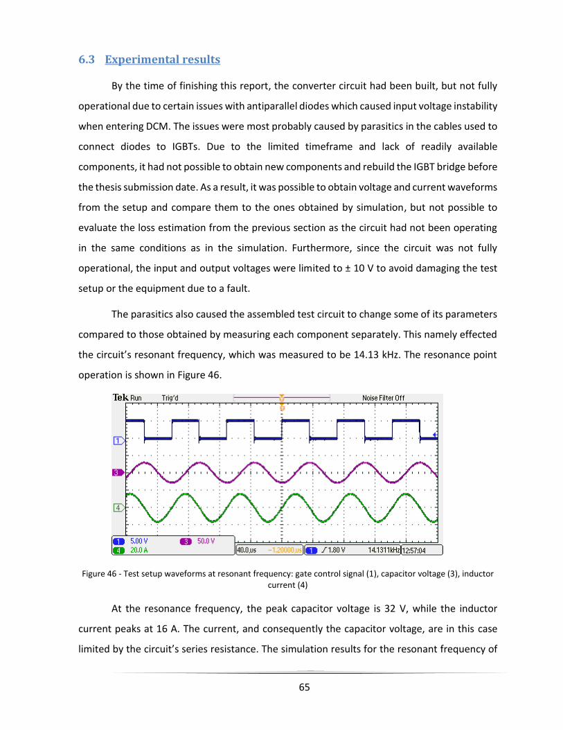
65
6.3 Experimental results
By the time of finishing this report, the converter circuit had been built, but not fully
operational due to certain issues with antiparallel diodes which caused input voltage instability
when entering DCM. The issues were most probably caused by parasitics in the cables used to
connect diodes to IGBTs. Due to the limited timeframe and lack of readily available
components, it had not possible to obtain new components and rebuild the IGBT bridge before
the thesis submission date. As a result, it was possible to obtain voltage and current waveforms
from the setup and compare them to the ones obtained by simulation, but not possible to
evaluate the loss estimation from the previous section as the circuit had not been operating
in the same conditions as in the simulation. Furthermore, since the circuit was not fully
operational, the input and output voltages were limited to ± 10 V to avoid damaging the test
setup or the equipment due to a fault.
The parasitics also caused the assembled test circuit to change some of its parameters
compared to those obtained by measuring each component separately. This namely effected
the circuit’s resonant frequency, which was measured to be 14.13 kHz. The resonance point
operation is shown in Figure 46.
Figure 46 - Test setup waveforms at resonant frequency: gate control signal (1), capacitor voltage (3), inductor current (4)
At the resonance frequency, the peak capacitor voltage is 32 V, while the inductor
current peaks at 16 A. The current, and consequently the capacitor voltage, are in this case
limited by the circuit’s series resistance. The simulation results for the resonant frequency of

66
the simulation circuit with old parameters is shown in Figure 47. The peak capacitor voltage
equals 37.6 V, while the peak inductor current 17.5 A. The results are fairly close to measured
values, which implies that the differences between the simulated and actual circuit are caused
by parasitic properties of wires and connectors used to connect the components together. The
wires connecting the components clearly increased the circuit’s series resistance, while the
frequency response could have been influenced by several factors, such as relative placement
of the components, wires and connectors itself or the addition of DC link capacitors for voltage
stabilization.
Figure 47 - Simulation results for test circuit with original parameters at resonant frequency
Measurements performed at resonant frequency confirmed the findings from section
4.2.2 stating that the highest component stress occurs at resonant frequency. However, due
to the circuit’s low quality factor, capacitor voltage peaked at only 3.2 times the input voltage.
Inductor current on the other hand reached fairly high values, drawing more than 100 W of
power from the 10 V input source.
Discontinuous conduction mode waveforms are shown in Figure 48. The figure depicts
filtered waveforms as the actual results had a lot of noise due to earlier stated problem with
the setup. Even so, obtained waveforms clearly reflect the waveforms obtained by simulations
from section 4.3, thus validating the principal model of series-resonant converter used.

67
Figure 48 - Test setup waveforms in DCM: gate control signal (1), capacitor voltage (3), inductor current (4)
The measurements confirm two biggest advantages of DCM. Peak capacitor voltage
equals 20 V, thus confirming relation (30) about the capacitor voltage being limited to twice
the input voltage in DCM. Comparing the inductor current waveform with the gate control
signal on the other hand confirms that both the IGBTs and diodes turn on and off at zero
current and therefore have minimal switching losses.
Figure 49 - Test setup waveforms in DCM: gate control signal (1), output current (4)
The output current waveform in DCM is shown in Figure 49. The second input is
unused. Once again, the waveforms coincide well with the ones obtained by simulation. The
output current equals the rectified inductor current scaled by the transformer’s transfer ratio.
The measurements confirm another statement from section 4.3 stating that peak-to-average
ratio of the output current in DCM is higher than in CCM.

68
Most important points stated in this chapter are the following:
Two important things that should be taken into account when building a real
SRC circuit are transformer saturation and the amount of dead time added
The laboratory circuit had excessive conduction losses due to skin effect and
unnecessarily high wire length, which is why stranded wire should be used to
wind and connect the components while the resonant tank inductor should be
included in the transformer’s leakage inductance
DCM converters maintain constant efficiency over the whole operating range
for stable input and output voltages
CCM is a better choice for low power circuits as they typically have high
conduction and low switching losses with only few or no device limitations
DCM is a better candidate for high power circuits due to device limitations,
higher characteristic switching losses and lower characteristic conduction
losses compared to low power circuits
Experimental results have validated several statements from section 4, such as
that peak component stress occurs at resonant frequency, DCM limits the peak
capacitor voltage to twice the input voltage, IGBTs and diodes switch at zero
current in DCM and peak-to-average value of output current is higher in DCM
than in CCM

69
7 Conclusion
This report contains the analysis, design procedure, simulation results and a lab setup
description of a series-resonant DC/DC converter circuit.
The converter circuit, even though inherently nonlinear, can be modelled using a set
of 3 equivalent linear circuits containing ideal voltage and current sources when the switching
frequency is close to the resonant frequency of the resonant tank.
The steady-state analysis has shown how the circuit responds to a change of input and
output voltages, switching frequency, duty cycle and resonant tank’s inductance and
capacitance. The biggest problems identified were high voltage and current stress on the
resonant tank components and the circuit’s nonlinear responsiveness the change of switching
frequency. A separate analysis was performed for the discontinuous conduction mode, which
reduces the component voltage stress and switching losses, but in return leads to increased
conduction losses. Power relations have been derived for both conduction modes and
revealed that another benefit of DCM is a linear relationship between the switching frequency
and the output power.
Based on the analysis’ results, general guidelines for series-resonant converter design
have been derived and used to make a 10 MW circuit proposal and its corresponding control
system. To analyze the characteristic losses of the converter, a 150 W lab prototype was built
and based on the measured parameters and component datasheets, the losses were
estimated in a Plecs simulation. The simulation revealed that the designed circuit had not been
optimized for higher frequencies and therefore had excessive copper losses.
Due to the limited timeframe and lack of readily available components, the lab setup
had not been fully operational before the project submission date and therefore a comparison
between the simulated and measured waveforms at full power has not been made. However,
measurements performed at reduced voltage levels have shown that voltage and current
waveforms of a test setup reflect the ones obtained by simulations. Main advantages of
discontinuous conduction mode – limited capacitor voltage and zero current switching have
also been experimentally validated.

70
Overall conclusion drawn from building the lab setup is that for converters of low size
and power, continuous conduction mode should be used as the conduction losses constitute
a dominant portion of the total power loss. For high power converters on the other hand,
device limitations and an increased share of switching losses make discontinuous conduction
mode a better candidate.

71
8 List of abbreviations
AC Alternating Current
CCM Continuous Conduction Mode
CD Compact Disc
DC Direct Current
DCM Discontinuous Conduction Mode
DT Dead Time
GUI Graphical User Interface
HV High Voltage
IGBT Insulated Gate Bipolar Transistor
LV Low Voltage
MF Medium Frequency
MV Medium Voltage
PI Proportional Integral
PWM Pulse Width Modulation
RMS Root Mean Square
SRC Series-Resonant Converter
72
9 References
[1] Fraunhofer ISE, Levelized Cost of Electricity: Renewable Energy
Technologies, Freiburg, Germany, 2013.
[2] R. Erickson and D. Maksimovic, Fundamentals of Power Electronics,
Boulder, Colorado: Kluwer Academic, 1997.
[3] N. Mohan, T. M. Undeland and W. P. Robbins, Power Electronics:
Converters, Applications and Design, John Wiley & Sons, Inc., 2002.
[4] D. Graovac and M. Purschel, "IGBT Power Losses Calculation Using the
Data-Sheet Parameters," Infineon Technologies AG, Neubiberg, Germany, 2009.
[5] U. Drofenik and J. W. Kolar, "A General Scheme for Calculating Switching-
and Conduction-Losses of Power Semiconductors in Numerical Circuit
Simulations of Power Electronic Systems," in International Power Electronics
Conference, Niigata, Japan, 2005.
[6] A. D. Rajapakse, A. M. Gole and P. L. Wilson, "Approximate Loss Formulae
for Estimation of IGBT Switching Losses through EMTP-type Simulations," in 6th
International Conference of Power System Transients, 2005.
[7] N. Soltau, D. Eggers, K. Hameyer and R. W. D. Doncker, "Iron Losses in a
Medium-Frequency Transformer Operated in a High-Power DC-DC Converter,"
IEEE Transactions on Magnetics, vol. 50, no. 2, 2014.
[8] I. Villar, I. Etxeberria-Otadui, U. Viscarret and A. Rufer, "Global Loss
Evaluation Methods for Nonsinusoidally Fed Medium-Frequency Power
Transformers," IEEE Transactions on Industrial Electronics, vol. 56, no. 10, pp.
4132-4140, 2009.

73
[9] G. Ortiz, M. Leibl, J. W. Kolar and O. Apeldoorn, "Medium Frequency
Transformers for Solid-State Applications: Design and Experimental Verification,"
in IEEE 10th International Conference on Power Electronics and Drive Systems,
2013.
[10] TDK, "Ferrites and accessories - SIFERRIT material N87," 2006.
[11] Silicon Labs, "0.5 and 4.0 Amp ISOdrivers Si823x," Silicon Laboratories Inc.,
Austin, Texas.
[12] Infineon, "IGW40T120 datasheet," Infineon Technologies AG, München,
Germany, 2009.
[13] Vishay, "VS-30CTH03-N3 datasheet," Vishay Semiconductors, 2012.
[14] Vishay, "VS-80EBU02 datasheet," Vishay Semiconductors, 2012.
[15] P. A. J. V. Rensburg and H. C. Ferreira, "The Role of Magnetizing and
Leakage Inductance in Transformer Coupling Circuitry," in 8th ISPLC, Zaragoza,
Spain, 2004.
[16] R. Nielsen, "LLC and LCC resonance converters: Properties, Analysis,
Control," Tommerup, Denmark, 2013.

74
10 Appendix
The CD handed in alongside this report contains the following:
Series-resonant converter analysis tool with GUI
Full plot catalogue from section 4.2
Plecs models of 150 W and 10 MW circuit
Lab component datasheets
This report in PDF