![arXiv:2106.05035v1 [cond-mat.mes-hall] 9 Jun 2021](https://static.fdocuments.us/doc/165x107/615b7196f5092405ea3f9bbd/arxiv210605035v1-cond-matmes-hall-9-jun-2021.jpg)
(Dated: November 1, 2011) arXiv:1110.6557v1 [cond-mat.mes ...
50
Experimental review of graphene Daniel R. Cooper, * Benjamin D’Anjou, Nageswara Ghattamaneni, Benjamin Harack, Michael Hilke, Alexandre Horth, Norberto Majlis, Mathieu Massicotte, Leron Vandsburger, Eric Whiteway, and Victor Yu McGill University, Montr´ eal, Canada, H3A 2T8 (Dated: November 1, 2011) This review examines the properties of graphene from an experimental perspective. The intent is to review the most important experimental results at a level of detail ap- propriate for new graduate students who are interested in a general overview of the fascinating properties of graphene. While some introductory theoretical concepts are provided, including a discussion of the electronic band structure and phonon disper- sion, the main emphasis is on describing relevant experiments and important results as well as some of the novel applications of graphene. In particular, this review cov- ers graphene synthesis and characterization, field-effect behavior, electronic transport properties, magneto-transport, integer and fractional quantum Hall effects, mechanical properties, transistors, optoelectronics, graphene-based sensors, and biosensors. This approach attempts to highlight both the means by which the current understanding of graphene has come about and some tools for future contributions. PACS numbers: 81.05.ue, 72.80.Vp, 63.22.Rc, 01.30.Rr CONTENTS I. Introduction 2 II. Electronic Structure 2 A. Massless Dirac fermions 3 B. Chirality 4 C. Klein paradox 4 D. Graphene vs traditional materials 4 III. Vibrational properties 5 A. Phonon dispersion 5 B. Thermal conductivity 7 IV. Synthesis 7 A. Mechanical exfoliation 7 B. Thermal decomposition of SiC 8 C. Chemical vapor deposition 8 1. Growth on nickel 8 2. Growth on copper 9 D. Molecular beam deposition 10 E. Unzipping carbon nanotubes 10 F. Sodium-ethanol pyrolysis 10 G. Other methods 10 H. Graphene oxide 10 1. Wet chemical synthesis 10 2. Plasma functionalization 11 3. RF plasma 11 4. Photoluminescence 11 V. Characterization 13 A. Raman spectroscopy 13 B. Optical microscopy 13 C. Electron microscopy 13 D. Measuring the electronic band structure 14 * Equal contributions from all authors VI. Electronic Transport and Field Effect 15 A. Measurement of the ambipolar field effect 16 B. Transport and scattering mechanisms 16 1. Phonon scattering 17 2. Coulomb scattering 17 3. Short-range scattering 18 C. Mobility 19 1. Graphene on SiO 2 19 2. Suspended graphene 19 3. Other substrates 20 D. Minimum conductivity 20 E. Other transport properties 21 VII. Magnetoresistance and Quantum Hall Effect 22 A. Experimental procedures 22 1. Setup 22 2. Carrier density tuning 23 3. Observation of the quantum Hall effect 23 B. Theoretical background 24 1. Chiral electrons and pseudospin 24 2. Landau levels 24 C. Measurements of weak localization and antilocalization in graphene 25 1. Quantum interferences 25 2. Measurements 25 D. Measurements of the quantum Hall effect in graphene 26 1. Shubnikov-de Haas oscillations 26 2. Conductance quantization 26 3. Integer quantum Hall effect 27 4. Fractional quantum Hall effect 29 VIII. Mechanical Properties 30 A. Overview of the harmonic oscillator 30 B. Tuning resonance frequency by electrical actuation 30 C. Resonance spectrum by optical actuation 31 D. Measurements by atomic force microscopy 33 IX. Graphene Transistors 34 A. Logic transistors 34 1. Bilayer graphene 34 arXiv:1110.6557v1 [cond-mat.mes-hall] 29 Oct 2011
Transcript of (Dated: November 1, 2011) arXiv:1110.6557v1 [cond-mat.mes ...

Experimental review of graphene
Daniel R. Cooper,∗ Benjamin D’Anjou, Nageswara Ghattamaneni, Benjamin Harack, Michael Hilke, AlexandreHorth, Norberto Majlis, Mathieu Massicotte, Leron Vandsburger, Eric Whiteway, and Victor Yu
McGill University,Montreal, Canada,H3A 2T8
(Dated: November 1, 2011)
This review examines the properties of graphene from an experimental perspective. Theintent is to review the most important experimental results at a level of detail ap-propriate for new graduate students who are interested in a general overview of thefascinating properties of graphene. While some introductory theoretical concepts areprovided, including a discussion of the electronic band structure and phonon disper-sion, the main emphasis is on describing relevant experiments and important resultsas well as some of the novel applications of graphene. In particular, this review cov-ers graphene synthesis and characterization, field-effect behavior, electronic transportproperties, magneto-transport, integer and fractional quantum Hall effects, mechanicalproperties, transistors, optoelectronics, graphene-based sensors, and biosensors. Thisapproach attempts to highlight both the means by which the current understanding ofgraphene has come about and some tools for future contributions.
PACS numbers: 81.05.ue, 72.80.Vp, 63.22.Rc, 01.30.Rr
CONTENTS
I. Introduction 2
II. Electronic Structure 2A. Massless Dirac fermions 3B. Chirality 4C. Klein paradox 4D. Graphene vs traditional materials 4
III. Vibrational properties 5A. Phonon dispersion 5B. Thermal conductivity 7
IV. Synthesis 7A. Mechanical exfoliation 7B. Thermal decomposition of SiC 8C. Chemical vapor deposition 8
1. Growth on nickel 82. Growth on copper 9
D. Molecular beam deposition 10E. Unzipping carbon nanotubes 10F. Sodium-ethanol pyrolysis 10G. Other methods 10H. Graphene oxide 10
1. Wet chemical synthesis 102. Plasma functionalization 113. RF plasma 114. Photoluminescence 11
V. Characterization 13A. Raman spectroscopy 13B. Optical microscopy 13C. Electron microscopy 13D. Measuring the electronic band structure 14
∗ Equal contributions from all authors
VI. Electronic Transport and Field Effect 15A. Measurement of the ambipolar field effect 16B. Transport and scattering mechanisms 16
1. Phonon scattering 172. Coulomb scattering 173. Short-range scattering 18
C. Mobility 191. Graphene on SiO2 192. Suspended graphene 193. Other substrates 20
D. Minimum conductivity 20E. Other transport properties 21
VII. Magnetoresistance and Quantum Hall Effect 22A. Experimental procedures 22
1. Setup 222. Carrier density tuning 233. Observation of the quantum Hall effect 23
B. Theoretical background 241. Chiral electrons and pseudospin 242. Landau levels 24
C. Measurements of weak localization andantilocalization in graphene 251. Quantum interferences 252. Measurements 25
D. Measurements of the quantum Hall effect ingraphene 261. Shubnikov-de Haas oscillations 262. Conductance quantization 263. Integer quantum Hall effect 274. Fractional quantum Hall effect 29
VIII. Mechanical Properties 30A. Overview of the harmonic oscillator 30B. Tuning resonance frequency by electrical actuation 30C. Resonance spectrum by optical actuation 31D. Measurements by atomic force microscopy 33
IX. Graphene Transistors 34A. Logic transistors 34
1. Bilayer graphene 34
arX
iv:1
110.
6557
v1 [
cond
-mat
.mes
-hal
l] 2
9 O
ct 2
011
2
2. Graphene nanoribbons 353. Other techniques 364. Techniques comparison 36
B. Analog transistors 36
X. Optoelectronics 37A. Optical properties 37B. Transparent conducting electrodes 38C. Graphene as TCE 39
1. Work function, Schottky junctions andphotodetectors 39
2. Light-emitting diodes 393. Photovoltaics 404. Graphene quantum dots (GQDs) and
graphene-QD nanocomposites 42
XI. Graphene Sensors 43A. Electrochemical sensors 44B. Graphene as a biosensor 45
XII. Conclusion 46
References 46
I. INTRODUCTION
Graphene is a single two-dimensional layer of carbonatoms bound in a hexagonal lattice structure. It has beenextensively studied in the last several years even thoughit was only isolated for the first time in 2004 (Novoselovet al., 2004). Andre Geim and Konstantin Novoselovwon the 2010 Nobel Prize in Physics for their ground-breaking work on graphene. The fast uptake of interestin graphene is due primarily to a number of exceptionalproperties that it has been found to possess.
There have been several reviews discussing the topicof graphene in recent years. Many are theoretically ori-ented, with Castro Neto et al.’s review of the electronicproperties as a prominent example (Castro Neto et al.,2009) and a more focused review of the electronic trans-port properties (Das Sarma et al., 2011). Experimentalreviews, to name only a few, include detailed discussionsof synthesis (Choi et al., 2010) and Raman character-ization methods (Ni et al., 2008a), of transport mech-anisms (Avouris, 2010; Giannazzo et al., 2011), of rel-evant applications of graphene such as transistors andthe related bandgap engineering (Schwierz, 2010), and ofgraphene optoelectronic technologies (Bonaccorso et al.,2010). We feel, however, that the literature is lacking acomprehensive overview of all major recent experimen-tal results related to graphene and its applications. Itis with the intent to produce such a document that wewrote this review. We gathered a great number of re-sults from what we believe to be the most relevant fieldsin current graphene research in order to give a startingpoint to readers interested in expanding their knowledgeon the topic. The review should be particularly well-suited to graduate students who desire an introductionto the study of graphene that will provide them withmany references for further reading.
We have attempted to deliver an up-to-date accountof most topics. For example, we present recent resultson the fractional quantum Hall effect and some of thenewest developments and device details in optoelectron-ics. In addition, we include a summary of the work thathas been done in the field of graphene biosensors. Asa practical tool, we also give comparative analyses ofgraphene substrate properties, of available bandgap en-gineering techniques and of photovoltaic devices in orderto provide the researcher with useful and summarizedlaboratory references.
This review is structured as follows: We start byreviewing the electronic band structure and its associ-ated properties in Sec. II before introducing the vibra-tional properties, including the phonon dispersion, inSec. III. We then detail the various synthesis methods forgraphene monolayers and their corresponding character-ization. The main properties are then discussed, startingwith the electric field effect, which originally spurred theintense activity in graphene research. This is then fol-lowed by a review of the magneto-transport properties,which includes the quantum Hall effect and recent resultson the fractional quantum Hall effect. We conclude thereview of the main properties with a discussion of the me-chanical properties of graphene, before turning to someimportant applications. The transistor applications arediscussed first, with particular emphasis on band gap en-gineering, before reviewing optoelectronic applications.We finish the applications section with a discussion ofgraphene-based sensors and biosensors.
II. ELECTRONIC STRUCTURE
Graphene has a remarkable band structure thanks toits crystal structure. Carbon atoms form a hexagonallattice on a two-dimensional plane. Each carbon atomis about a = 1.42 A from its three neighbors, with eachof which it shares one σ bond. The fourth bond is aπ-bond, which is oriented in the z-direction (out of theplane). One can visualize the π orbital as a pair of sym-metric lobes oriented along the z-axis and centered on thenucleus. Each atom has one of these π-bonds, which arethen hybridized together to form what are referred to asthe π-band and π∗-bands. These bands are responsiblefor most of the peculiar electronic properties of graphene.
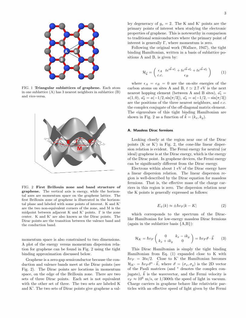
The hexagonal lattice of graphene can be regarded astwo interleaving triangular lattices. This is illustrated inFig. 1. This perspective was successfully used as far backas 1947 when Wallace calculated the band structure for asingle graphite layer using a tight-binding approximation(Wallace, 1947).
Band structure is most often studied from a standpointof the relationship between the energy and momentumof electrons within a given material. Since graphene con-strains the motion of electrons to two dimensions, our
3
FIG. 1 Triangular sublattices of graphene. Each atomin one sublattice (A) has 3 nearest neighbors in sublattice (B)and vice-versa.
FIG. 2 First Brillouin zone and band structure ofgraphene. The vertical axis is energy, while the horizon-tal axes are momentum space on the graphene lattice. Thefirst Brillouin zone of graphene is illustrated in the horizon-tal plane and labeled with some points of interest. K and K’are the two non-equivalent corners of the zone, and M is themidpoint between adjacent K and K’ points. Γ is the zonecenter. K and K’ are also known as the Dirac points. TheDirac points are the transition between the valence band andthe conduction band.
momentum space is also constrained to two dimensions.A plot of the energy versus momentum dispersion rela-tion for graphene can be found in Fig. 2 using the tightbinding approximation discussed below.
Graphene is a zero-gap semiconductor because the con-duction and valence bands meet at the Dirac points (seeFig. 2). The Dirac points are locations in momentumspace, on the edge of the Brillouin zone. There are twosets of three Dirac points. Each set is not equivalentwith the other set of three. The two sets are labeled Kand K’. The two sets of Dirac points give graphene a val-
ley degeneracy of gv = 2. The K and K’ points are theprimary points of interest when studying the electronicproperties of graphene. This is noteworthy in comparisonto traditional semiconductors where the primary point ofinterest is generally Γ, where momentum is zero.
Following the original work (Wallace, 1947), the tightbinding Hamiltonian, written in a basis of sublattice po-sitions A and B, is given by:
H~k =
(εA tei
~k· ~a1 + tei~k· ~a2 + tei
~k· ~a3
c.c. εB
)(1)
where εA = εB = 0 are the on-site energies of thecarbon atoms on sites A and B, t ' 2.7 eV is the nextnearest hopping element (between A and B sites), ~a1 =a(1, 0), ~a2 = a(−1/2, sin[π/3]), ~a3 = a(−1/2,− sin[π/3])are the positions of the three nearest neighbors, and c.c.the complex conjugate of the off-diagonal matrix element.The eigenvalues of this tight binding Hamiltonian areshown in Fig. 2 as a function of ~k = (kx, ky).
A. Massless Dirac fermions
Looking closely at the region near one of the Diracpoints (K or K’) in Fig. 2, the cone-like linear disper-sion relation is evident. The Fermi energy for neutral (orideal) graphene is at the Dirac energy, which is the energyof the Dirac point. In graphene devices, the Fermi energycan be significantly different from the Dirac energy.
Electrons within about 1 eV of the Dirac energy havea linear dispersion relation. The linear dispersion re-gion is well-described by the Dirac equation for masslessfermions. That is, the effective mass of the charge car-riers in this region is zero. The dispersion relation nearthe K points is generally expressed as follows:
E±(k) ≈ ±hvF |k −K| (2)
which corresponds to the spectrum of the Dirac-like Hamiltonian for low-energy massless Dirac fermions(again in the sublattice basis A,B):
HK = hvF
(0 kx − iky
kx + iky 0
)= hvF~σ · ~k (3)
This Dirac Hamiltonian is simply the tight bindingHamiltonian from Eq. (1) expanded close to K withhvF = 3ta/2. Close to K’ the Hamiltonian becomes
HK′ = hvF~σ∗ · ~k, where ~σ = (σx, σy) is the 2D vector
of the Pauli matrices (and ∗ denotes the complex con-
jugate), ~k is the wavevector, and the Fermi velocity isvF ≈ 106 m/s, or 1/300th the speed of light in vacuum.Charge carriers in graphene behave like relativistic par-ticles with an effective speed of light given by the Fermi

4
velocity. This behavior is one of the most intriguing as-pects about graphene, and is responsible for much of theresearch attention that graphene has received.
B. Chirality
Transport in graphene exhibits a novel chirality whichwe will now briefly describe. Each graphene sublatticecan be regarded as being responsible for one branch ofthe dispersion. These dispersion branches interact veryweakly with one another.
This chiral effect indicates the existence of a pseu-dospin quantum number for the charge carriers. Thisquantum number is analogous to spin but is completelyindependent of the ‘real’ spin. The pseudospin lets usdifferentiate between contributions from each of the sub-lattices. This independence is called chirality becauseof the inability to transform one type of dispersion intoanother (Das Sarma et al., 2011). A typical example ofchirality is that you cannot transform a right hand into aleft hand with only translations, scalings, and rotations.The chirality of graphene can also be understood in termsof the Pauli matrix contributions in the Dirac-like Hamil-tonian described in the previous section.
C. Klein paradox
A peculiar property of the Dirac Hamiltonian is thatcharge carriers cannot be confined by electrostatic po-tentials. In traditional semiconductors, if an electronstrikes an electrostatic barrier that has a height above theelectron’s kinetic energy, the electron wavefunction willbecome evanescent within the barrier and exponentiallydecay with distance into the barrier. This means thatthe taller and wider a barrier is, the more the electronwavefunction will decay before reaching the other side.Thus, the taller and wider the barrier is, the lower theprobability of the electron quantum tunneling throughthe barrier.
However, if the particles are governed by the Diracequation, their transmission probability actually in-creases with increasing barrier height. A Dirac electronthat hits a tall barrier will turn into a hole, and propagatethrough the barrier until it reaches the other side, whereit will turn back into an electron. This phenomenon iscalled Klein tunneling.
An explanation for this phenomenon is that increas-ing barrier height leads to an increased degree of mode-matching between the wavefunctions of the holes withinthe barrier and the electrons outside of it. When themodes are perfectly matched (in the case of an infinitelytall barrier), we have perfect transmission through thebarrier. In the case of graphene, the chirality discussedearlier leads to a varying transmission probability de-
pending on the angle of incidence to the barrier (Kat-snelson et al., 2006).
Some experimental results have been interpreted as ev-idence for Klein tunneling. Klein tunneling has been ob-served through electrostatic barriers, which were createdby gate voltages (Stander et al., 2009). Similar effectshave also been observed in narrow graphene resonant het-erostructures (Young and Kim, 2009).
D. Graphene vs traditional materials
Here we summarize some of the interesting propertiesof graphene by comparing them with more traditionalmaterials such as 2D semiconductors.
1. Traditional semiconductors have a finite band gapwhile graphene has a nominal gap of zero. Nor-mally, the study of electron and hole motionthrough a semiconductor must be done with dif-ferently doped materials. However, in graphenethe nature of a charge carrier changes at the Diracpoint from an electron to a hole or vice-versa. Ona related note, the Fermi level in graphene is al-ways within the conduction or valence band whilein traditional semiconductors the Fermi level oftenfalls within the band gap when pinned by impuritystates.
2. Dispersion in graphene is chiral. This is related tosome very distinctive material behaviors like Kleintunneling.
3. Graphene has a linear dispersion relation whilesemiconductors tend to have quadratic dispersion.Many of the impressive physical and electronicproperties of graphene can be considered to be con-sequences of this fact.
4. Graphene is much thinner than a traditional 2Delectron gas (2DEG). A traditional 2DEG in aquantum well or heterostructure tends to have aneffective thickness around 5-50 nm. This is due tothe constraints on construction and the fact thatthe confined electron wavefunctions have an evanes-cent tail that stretches into the barriers. Grapheneon the other hand is only a single layer of carbonatoms, generally regarded to have a thickness ofabout 3 A (twice the carbon-carbon bond length).Electrons conducting through graphene are con-strained in the z-axis to a much greater extent thanthose that conduct through a traditional 2DEG.
5. Graphene has been found to have a finite minimumconductivity, even in the case of vanishing chargecarriers (Novoselov et al., 2005; Tan et al., 2007).This is an issue for the construction of field-effecttransistors (FETs), as we will see in more detail

5
in section VI, since it contributes to relatively lowon/off ratios for graphene-based transistors.
Readers seeking further reading about distinctly elec-tronic properties of graphene should refer to Sec. VI. Thenext section will introduce and discuss the vibrationalproperties of graphene.
III. VIBRATIONAL PROPERTIES
While the electronic properties have attracted thelion’s share of the interest in graphene, the vibrationalproperties are of great importance too. They are re-sponsible for several fascinating properties such as recordthermal conductivities. Since graphene is composed of alight atom, where the in-plane bonding is very strong,graphene exhibits a very high sound velocity. This largesound velocity is responsible for the very high thermalconductivity of graphene that is useful in many appli-cations. Moreover, vibrational properties are instrumen-tal in understanding other graphene attributes, includingoptical properties via phonon-photon scattering (e.g. inRaman scattering) and electronic properties via electron-phonon scattering.
A. Phonon dispersion
Most of the vibrational properties of graphene can beunderstood with the help of the phonon dispersion re-lation. Interestingly, the phonon dispersion has somesimilarity with the electronic band structure discussedin the previous section, which stems from the identicalhoneycomb structure (the out-of-plane modes are shownin Fig. 3). In order to obtain the phonon dispersion it isnecessary to consider the vibrational modes of the crys-tal in thermal equilibrium. This is done by consideringthe displacement of each atom from its equilibrium po-sition, written ~un for the atom labeled n. Each atomis effectively coupled to its neighbors by some torsionaland longitudinal force constants, which only depend onthe relative positions of the atoms. This allows one towrite the Newtonian coupled equation of motion in fre-quency space as:
−∑m
Φm,n~un = ω2~un, (4)
where in graphene the sum over m is typically overthe second or fourth nearest neighbors, with the corre-sponding coefficients Φm,n, also known as the dynamicalmatrix.
In graphene, and similarly to the electronic structure,the two sublattices A and B have to be considered ex-plicitly to solve for the eigenspectrum of the dynamical
matrix. However, the atoms can vibrate in all three di-mensions, hence the dynamical matrix has to be writtenin terms of both the sublattices A and B as well as the 3spatial dimensions. This leads to a dynamical matrix inreciprocal space Φm,n(~k), which is given by a 6 × 6 ma-
trix when assuming ~uA,Bn ∼ ei~k·~RA,Bn . Here one applies
Bloch’s theorem, where ~RA,Bn is the equilibrium positionof atom n in the sublattice A and B, respectively. Two ofthe eigenvalues correspond to the out-of-plane vibrations,ZA (acoustic) and ZO (optical), and the remaining 4 cor-respond to the in-plane vibrations: TA (transverse acous-tic), TO (transverse optical), LA (longitudinal acoustic)and LO (longitudinal optical).
FIG. 3 First Brillouin zone and out-of-plane phononmodes. The phonon dispersion relation of the ZA and ZO
modes as a function of the in-plane reciprocal vector ~k. Thevertical axis is the phonon frequency, while the horizontal axesare momentum space on the graphene lattice. The dispersionrelation is obtained using the second-nearest-neighbor modelfor graphene (Falkovsky, 2007). The gray surface correspondsto the ZO (optical) mode, whereas the pink surface shows theZA (acoustic) mode. Also shown are the corresponding K, Γ,and M points of the Brillouin zone.
The ZA and ZO modes are often assumed to be decou-pled from the in-plane modes (Falkovsky, 2007), whichleads to a simple dispersion relation very similar to theelectronic band structure as shown in Fig. 3. It is inter-esting to note that the dispersion is quadratic at the Γpoint, which is unusual for acoustic modes. In contrast,a simple graphene phonon model based on atomic poten-tials containing only three parameters leads to a lineardispersion for the ZA mode (Adamyan and Zavalniuk,2011). However, the experimental data seems to be moreconsistent with a quadratic dispersion (see Fig. 5) (Dres-selhaus and Eklund, 2000; Popov, 2004). At the K andK’ points we recover a cone structure similar to the Diraccones in the electronic structure. However, the phonon

6
density of states does not vanish at these points becauseof the presence of the in-plane modes.
FIG. 4 First Brillouin zone and in-plane phononmodes. The phonon dispersion relation of the TO and LOmodes in gray and the TA and LA modes in pink as a function
of the in-plane reciprocal vector ~k. The longitudinal modesare on top of the transverse modes. The vertical axis is thephonon frequency, while the horizontal axes are the momen-tum space on the graphene lattice.
The in-plane modes are constituted by two acousticmodes and two optical modes. These modes can beobtained from the reduced in-plane dynamical matrix,which can be described by a 4 × 4 matrix, assuming nocoupling to the out-of-plane modes. Using the param-eters given by reference (Falkovsky, 2007), the in-planemodes are shown in Fig. 4.
FIG. 5 Experimental phonon dispersion relation ingraphite. All the phonon modes are shown, including thein-plane and out-of-plane modes. The data (full symbols) isshown along the special symmetry points Γ, K, and M alongwith results from ab initio calculations (lines). Figure adaptedfrom (Wirtz and Rubio, 2004).
The in-plane modes show the expected linear disper-sion at the Γ point. The transverse modes closely fol-
low the longitudinal modes but with a slightly lower fre-quency, for both the acoustic and optical modes. Forcomparison with experiments, it is more instructive toshow the dispersion relation following surface cuts alongthe lines Γ to M, M to K and K to Γ in the Brillouinzone. An extensive collection of experimental data forgraphite is shown in Fig. 5 along with ab initio calcula-tions. The data was obtained using several techniques,including neutron scattering, electron energy loss spec-troscopy, X-ray scattering, infrared absorption and dou-ble resonant Raman scattering experiments (Wirtz andRubio, 2004). There is no comparably extensive data ongraphene yet, but it is expected to be very similar tographite, since the coupling between planes is very weak.
FIG. 6 Theoretical phonon dispersion of graphene andRaman spectrum of large scale graphene. The labels(G, D, 2D, etc) identify the peaks from the Raman spectrumwith the corresponding phonon energies (Rao et al., 2011;Venezuela et al., 2011). Only the in-plane modes are shownsince they are the only ones which are Raman active. SeveralRaman data sets of graphene 13C are shown in blue takenfrom different spots of the same sample at a laser wavelengthof 514nm. The red line corresponds to the average over thesedata sets. The phonon dispersion is calculated using the massof 13C.
Most of the data on graphene stems from Raman scat-tering, which allows for the determination of the phononspectrum close to special symmetry points. This is illus-
7
trated in Fig. 6, where the theoretical phonon dispersionwith parameters from (Falkovsky, 2007) is shown withthe labels corresponding to the various Raman peaks.The Raman peaks determine the phonon energies forsome values of the momentum. The Raman data was ob-tained from chemical vapor deposition (CVD) 13C growngraphene. More conventional 12C graphene is very simi-lar except for a rescaling of the Raman peaks due to thechange of mass. Other aspects of the Raman spectrumare discussed in Sec. V.
An important consequence of the phonon dispersion re-lation in graphene is the very high value of the in-planesound velocity, close to cph ' 20 km/s (Adamyan andZavalniuk, 2011), which leads to very high thermal con-ductivities.
B. Thermal conductivity
From the kinetic theory of gases, the thermal con-ductivity due to phonons is given by κ ∼ cph CV (T ) λ,where CV (T ) is the specific heat per unit volume and λis the phonon mean free path. This implies that sincecph is very large in graphene, one can expect a largethermal conductivity. Indeed, experiments at near roomtemperature obtain κ ' 3080-5150 W/mK and a phononmean free path of λ ' 775 nm for a set of grapheneflakes (Balandin et al., 2008; Ghosh et al., 2008).
These results indicate that graphene is a good can-didate for applications to electronic devices, since ahigh thermal conductivity facilitates the diffusion of heatto the contacts and allows for more compact circuits.Phonons also play an important role in electronic trans-port via electron-phonon scattering, which is discussedin Sec. VI. The mechanical properties of graphene arediscussed in Sec. VIII, whereas the synthesis of grapheneis treated in the next section.
IV. SYNTHESIS
Since graphene was isolated in 2004 by Geim andNovoselov using the now famous Scotch tape method,there have been many processes developed to producefew-to-single layer graphene. One of the primary con-cerns in graphene synthesis is producing samples withhigh carrier mobility and low density of defects. To datethere is no method that can match mechanical exfoliationfor producing high-quality, high-mobility graphene flakes.However, mechanical exfoliation is a time consuming pro-cess limited to small scale production. There is great in-terest in producing large scale graphene suitable for ap-plications in flexible transparent electronics, transistors,etc. Some concerns in producing large scale graphene arethe quality and consistency between samples as well as
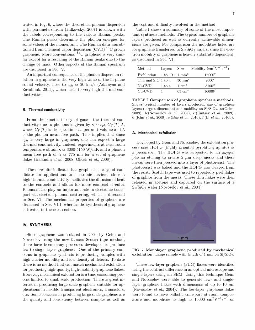
the cost and difficulty involved in the method.Table I shows a summary of some of the most impor-
tant synthesis methods. The typical number of graphenelayers produced as well as currently achievable dimen-sions are given. For comparison the mobilities listed arefor graphene transferred to Si/SiO2 wafers, since the elec-tron mobility of graphene is heavily substrate dependent,as discussed in Sec. VI.
Method Layers Size Mobility (cm2V−1s−1)
Exfoliation 1 to 10+ 1 mma 15000b
Thermal SiC 1 to 4 50 µmc 2000c
Ni-CVD 1 to 4 1 cmd 3700d
Cu-CVD 1 65 cme 16000f
TABLE I Comparison of graphene synthesis methods.Shows typical number of layers produced, size of graphenelayers (largest dimension) and mobility on Si/SiO2. a:(Geim,2009), b:(Novoselov et al., 2005), c:(Emtsev et al., 2009),d:(Kim et al., 2009), e:(Bae et al., 2010), f:(Li et al., 2010b).
A. Mechanical exfoliation
Developed by Geim and Novoselov, the exfoliation pro-cess uses HOPG (highly oriented pyrolitic graphite) asa precursor. The HOPG was subjected to an oxygenplasma etching to create 5 µm deep mesas and thesemesas were then pressed into a layer of photoresist. Thephotoresist was baked and the HOPG was cleaved fromthe resist. Scotch tape was used to repeatedly peel flakesof graphite from the mesas. These thin flakes were thenreleased in acetone and captured on the surface of aSi/SiO2 wafer (Novoselov et al., 2004).
FIG. 7 Monolayer graphene produced by mechanicalexfoliation. Large sample with length of 1 mm on Si/SiO2.
These few-layer graphene (FLG) flakes were identifiedusing the contrast difference in an optical microscope andsingle layers using an SEM. Using this technique Geimand Novoselov were able to generate few- and single-layer graphene flakes with dimensions of up to 10 µm(Novoselov et al., 2004). The few-layer graphene flakeswere found to have ballistic transport at room temper-ature and mobilities as high as 15000 cm2V−1s−1 on

8
Si/SiO2 wafers (Novoselov et al., 2005). The scotch tapemethod can generate flakes with sides of up to 1 mm inlength (Geim, 2009), of excellent quality and well suitedfor fundamental research. However, the process is lim-ited to small sizes and cannot be scaled for industrialproduction.
B. Thermal decomposition of SiC
The thermal decomposition of silicon carbide is a tech-nique that consists of heating SiC in ultra-high vacuum(UHV) to temperatures between 1000C and 1500C.This causes Si to sublimate from the material and leavebehind a carbon rich surface. Low-energy electron mi-croscopy (LEEM) studies indicate that this carbon layeris graphitic in nature, which suggests that the techniquecould be used to form graphene (Hass et al., 2008).
Berger and De Heer produced few-layer graphene bythermal decomposition of SiC. The Si face of a 6H-SiCsingle crystal was first prepared by oxidation or H2 etch-ing in order to improve surface quality. The sample wasthen heated by electron bombardment in UHV to 1000Cto remove the oxide layer. Once the oxide was removedthe samples were heated to 1250-1450C, resulting in theformation of thin graphitic layers. Typically between 1and 3 layers were formed depending on the decompositiontemperature. Using this method, devices were producedwith mobilities of 1100 cm2V−1s−1 (Berger et al., 2004).
This technique is capable of generating wafer-scalegraphene layers and is potentially of interest to the semi-conductor industry. Several issues still remain, notablycontrolling the number of layers produced, repeatabilityof large area growths and interface effects with the SiCsubstrate (Choi et al., 2010).
Emtsev et al. found that by heating SiC in Ar at 900mbar as opposed to UHV they were able to reduce surfaceroughness and produce much larger continuous graphenelayers, up to 50 µm in length. The graphene on SiCwas characterized using atomic force microscopy (AFM)and LEEM, as shown in Fig. 8. They measured electronmobilities of up to 2000 cm2V−1s−1 (Emtsev et al., 2009).
Juang et al. synthesized millimeter size few- to single-layer graphene sheets using SiC substrate coated in a thinNi film. 200 nm of Ni was evaporated onto the surface ofthe SiC and the sample was heated to 750C in vacuum.Graphene was found to segregate to the surface of the Nion cooling. This gave a continuous graphene layer overthe entire nickel surface (Juang et al., 2009).
Unarunotai et al. have developed a technique to trans-fer graphene synthesized on SiC onto arbitrary insulatingsubstrates. Graphene was first produced using a typicalthermal decomposition of SiC technique. A bilayer filmof gold/polyimide was deposited onto the SiC wafer andthen peeled off. The gold/polyimide film was then trans-ferred onto a Si/SiO2 substrate and the gold/polyimide
FIG. 8 Graphene produced by thermal decompositionof SiC. (a) AFM image of graphene growth on SiC annealedat UHV. (b) LEEM image of UHV grown graphene film. (c)AFM image of graphene annealed in Ar at 900 mbar. (d)LEEM image of graphene on Ar annealed SiC substrate show-ing terraces up to 50 µm in length (Emtsev et al., 2009).
layers were removed using oxygen plasma reactive ionetching. This yielded single-layer graphene flakes withmm2 areas (Unarunotai et al., 2009).
C. Chemical vapor deposition
In contrast to the thermal decomposition of SiC, wherecarbon is already present in the substrate, in chemicalvapor deposition (CVD), carbon is supplied in gas formand a metal is used as both catalyst and substrate togrow the graphene layer.
1. Growth on nickel
Yu et al. grew few-layer graphene sheets on polycrys-talline Ni foils. The foils were first annealed in hydrogenand then exposed to a CH4-Ar-H2 environment at atmo-spheric pressure for 20 mins at a temperature of 1000C.The foils were then cooled at different rates between20C/s and 0.1C/s. The thickness of the graphene layerswas found to be dependent on the cooling rate, with few-layer graphene (typically 3-4 layers) being produced witha cooling rate of 10C/s. Faster cooling rates result inthicker graphite layers, whereas slower cooling preventscarbon from segregating to the surface of the Ni foil (Yuet al., 2008).
To transfer the graphene layers to an insulating sub-strate, the Ni foil with graphene was first coated in sil-icone rubber and covered with a glass slide then the Niwas etched in HNO3.

9
2. Growth on copper
Li et al. used a similar process to produce large scalemonolayer graphene on copper foils. 25 µm thick copperfoils were first heated to 1000C in a flow of 2 sccm (stan-dard cubic centimeters per minute) hydrogen at low pres-sure and then exposed to methane flow of 35 sccm andpressure of 500 mTorr. Raman spectroscopy and SEMimaging confirm the graphene to be primarily monolayerindependent of growth time. This indicates that the pro-cess is surface mediated and self limiting. They fabri-cated dual gated FETs using graphene and extracted acarrier mobility of 4050 cm2V−1s−1 (Li et al., 2009).
Recently a roll-to-roll process was demonstrated toproduce graphene layers with a diagonal of up to 30inches as well as transfer them to transparent flexiblesubstrates (Bae et al., 2010). Graphene was grown byCVD on copper, and a polymer support layer was ad-hered to the graphene-copper. The copper was then re-moved by chemical etching and the graphene film trans-ferred to a polyethylene terephthalate (PET) substrate.These films demonstrate excellent sheet resistances of 125Ω/2 for a single layer. Using a repeated transfer process,doped 4-layer graphene sheets were produced with sheetresistances as low as 30 Ω/2 and optical transmittancegreater than 90%. These 4-layer graphene sheets are su-perior to commercially available indium tin oxide (ITO)currently used in flat panel displays and touch screens interms of sheet resistance (∼100 Ω/2 for ITO) and opticaltransmittance (∼90% for ITO).
FIG. 9 Multiple CVD graphene sheets transferred toPET. A roll-to-roll process was used to produce graphenesheets with up to 30 inch diagonal (Bae et al., 2010).
Li et al. have shown the dependence on the size ofgraphene domains synthesized by CVD with tempera-ture, methane flow and methane pressure. Performingthe growth at 1035C with methane flow of 7 sccm andpressure 160 mTorr led to the largest graphene domainswith average areas of 142 µm2. A two-step process was
used to first grow large graphene flakes and then by mod-ifying the growth conditions to fill in the gaps in thegraphene sheet. Using this technique they were able toproduce samples with carrier mobility of up to 16000cm2V−1s−1 (Li et al., 2010b). In general, the graphenelayer is slightly strained on the copper foil due to thehigh temperature growth (Yu et al., 2011).
FIG. 10 Controlling domain size in CVD graphene. Ef-fect of temperature, methane flow and methane partial pres-sure on the size of graphene domains in CVD growth, scalebars are 10 µm (Li et al., 2010b).
Recently Lee et al. have demonstrated a techniqueto produce uniform bilayer graphene by chemical vapordeposition on copper using a similar process but withmodified growth conditions. They determined optimalbilayer growth conditions to be: 15 minutes at 1000Cwith methane flow of 70 sccm and pressure of 500 mTorr.The bilayer nature of the graphene was confirmed by Ra-man spectroscopy, AFM, and transmission electron mi-croscopy (TEM). Electrical transport measurements in adual gated device indicate that a band gap is opened inCVD bilayer graphene (Lee et al., 2010).

10
FIG. 11 Bilayer CVD growth on copper. (a) 2 x 2 inchbilayer graphene on Si/SiO2. (b) Raman spectrum with 514nm laser source of 1 and 2 layers of graphene produced byexfoliation and CVD (Lee et al., 2010).
D. Molecular beam deposition
Zhan et al. succeeded in layer-by-layer growth ofgraphene using a molecular beam deposition technique.Starting with an ethylene gas source, gas was brokendown at 1200C using a thermal cracker and depositedon a nickel substrate. Large area, high quality graphenelayers were produced at 800C. This technique is capableof forming one layer on top of another, allowing for syn-thesis of one to several layers of graphene. The numberof graphene layers produced was found to be independentof cooling rate, indicating that carbon was not absorbedinto the bulk of the Ni as in CVD growth on nickel.Results were confirmed using Raman spectroscopy andTEM (Zhan et al., 2011).
FIG. 12 Molecular beam deposition producedgraphene. (a) Diagram of thermal cracker setup. (b) TEMimage of graphene film, scale bar 100 nm (Zhan et al., 2011).
E. Unzipping carbon nanotubes
Multi-walled carbon nanotubes were cut longitudinallyby first suspending them in sulphuric acid and then treat-ing them with KMnO4. This produced oxidized graphenenanoribbons which were subsequently reduced chemi-cally. The resulting graphene nanoribbons were foundto be conducting, but electronically inferior to large scalegraphene sheets due to the presence of oxygen defect sites(Kosynkin et al., 2009).
F. Sodium-ethanol pyrolysis
Graphene was produced by heating sodium andethanol at a 1:1 molar ratio in a sealed vessel. The prod-uct of this reaction is then pyrolized to produce a materialconsisting of fused graphene sheets, which can then be re-leased by sonication. This yielded graphene sheets withdimensions of up to 10 µm. The individual layer, crys-talline and graphitic nature of the samples was confirmedby TEM, selected area electron diffraction (SAED) andRaman spectroscopy (Choucair et al., 2009).
G. Other methods
There are several other ways to produce graphene suchas electron beam-irradiation of PMMA nanofibres (Duanet al., 2008), arc discharge of graphite (Subrahmanyamet al., 2009), thermal fusion of PAHs (Wang et al., 2008a),and conversion of nanodiamond (Subrahmanyam et al.,2008).
H. Graphene oxide
Another approach to the production of graphene is son-ication and reduction of graphene oxide (GO). The polarO and OH groups formed during the oxidation processrender graphite oxide hydrophilic, and it can be chemi-cally exfoliated in several solvents, including water (Zhuet al., 2010). The graphite oxide solution can then besonicated in order to form GO nanoplatelets. The oxy-gen groups can then be removed in a reduction processinvolving one of several reducing agents. This methodwas used by Stankovich et al. using a hydrazine reduc-ing agent, but the reduction process was found to beincomplete, leaving some oxygen remaining (Stankovichet al., 2007).
Graphene oxide (GO) is produced as a precursor tographene synthesis. GO is useful because its individuallayers are hydrophilic, in contrast to graphite. GO is sus-pended in water by sonication (McAllister et al., 2007;Paredes et al., 2008), then deposited onto surfaces byspin coating or filtration to make single or double layergraphene oxide. Graphene films are then made by re-ducing the graphene oxide either thermally or chemically(Marcano et al., 2010). The exact structure of grapheneoxide is still a matter of debate, although there is consid-erable agreement as to the general types and proportionof oxygen bonds present in the graphene lattice (He et al.,1996).
1. Wet chemical synthesis
The chemical methods to produce GO were all devel-oped before 1960. The most recent and most commonly

11
employed is the Hummers procedure (Hummers and Offe-man, 1958). This process treats graphite in an anhydrousmixture of sulfuric acid, sodium nitrate, and potassiumpermanganate for several hours, followed by the addi-tion of water. The resulting material is graphite oxidehydrate, which contains approximately 23% water. Sub-sequent nuclear magnetic resonance and X-ray diffractionstudies of the structure of GO have led to fairly detailedmodels based on a combination of hydroxide, carbonyl,carboxyl and epoxide groups covalently bonded to thegraphene lattice. Fig. 13 shows a predicted structurefor GO produced using the Hummers method (He et al.,1998).
FIG. 13 Structure of a monolayer of graphite oxide (Heet al., 1998).
FIG. 14 Summary of the Hummers method and ther-mal reduction. Bulk graphite is oxidized then separatedin water. Then it is thermally reduced to make single-layergraphene (McAllister et al., 2007).
Understandably, the degree of oxidation strongly af-fects the in-plane electrical and thermal conductivity ofgraphene oxide. Increased introduction of oxygen groupsinto the graphene lattice interrupts the sp2 hybridiza-tion of electron orbitals. Epoxide groups can be reducedby thermal treatment, or reaction with potassium iodide(KI), leading to a similar structure, where only hydroxylgroups are present. This leads to improved electrical con-ductivity and unaffected hydrophilicity. In each case theprocedure requires tight temperature control and longreaction times of several hours. The basic process, in-cluding thermal treatment, is shown in Fig. 14.
2. Plasma functionalization
Following the realization of the potential importanceof graphene as a replacement for semiconductor materi-als and indium tin oxide (ITO), as discussed in Sec. X.B,alternative methods for graphene production have beenexplored. Other approaches have been sought to producethe same hydrophilicity in graphite without the time andmaterial requirements of the Hummers method. Very re-cently, glow discharge treatment has been proven to in-troduce oxygen species into the lattices of all forms ofgraphitic materials (e.g. buckyballs, CNTs, graphene,carbon nanofibers, and graphite) (Vandsburger et al.,2009). The resulting graphene/graphite oxides have astructure very similar to Hummers GO, and can be ther-mally treated to selectively reduce epoxides. Unlike theHummers method, plasma functionalization requires nostrong acids, can proceed at room temperature and canbe completed very quickly, often in a matter of secondsor minutes.
Aside from its potential to replace the Hummersmethod, plasma treatment in itself is interesting for al-tering the electrical conductivity of graphene or thingraphite. This allows for bandgap engineering as wellas phenomena like photoluminescence (PL).
3. RF plasma
Radio frequency (RF) plasma refers to a processingtechnique whereby a capacitive plasma is ignited in anisolated volume. RF treatment is used almost exclusivelyfor surface treatment of graphene, because ion bombard-ment is significantly reduced in RF treatments, as op-posed to DC discharges. In RF plasma, electrodes neednot be in contact with the plasma gas, current is sup-plied with an alternation frequency of 13.57 MHz, andpower ranges from 10 W to 50 W. RF treatment hasbeen shown to selectively affect the outermost surface ofgraphene (Hazra et al., 2011). Other work using onlyoxygen for RF treatment allows for layer-by-layer etch-ing of a graphite surface, producing islands of GO (Youet al., 1993).
4. Photoluminescence
Single- and dual-layer graphene do not exhibit photo-luminescence, due mainly to the negligible bandgap ofnative graphene. GO does have a photoluminescent re-sponse, but the typical oxidation methods, sonication ofbulk graphite oxide, are inappropriate for use in photo-luminescence applications. For that reason, RF plasmaoxidation has been the subject of recent work at produc-ing photoluminescent single layers of GO. The procedurefor producing GO thin films from single layer graphene

12
was reported in (Gokus et al., 2009). Rather than oxi-dizing bulk graphite to produce single layers of graphene,single- or few-layer graphene is oxidized after isolation.Typically, graphene is prepared by micro-cleavage usingthe scotch tape or other methods, and electrical contactsor other additions are put in place. Following installa-tion, RF plasma treatment in Ar-O2 mixes is applied inone to six second intervals. The plasma power reportedwas 10 W, the pressure 0.04 mbar, and the gas composi-tion ratio was 2:1 Ar to O2.
An important finding reported by (Childres et al.,2011) is the temporal evolution of the Raman spectrumof graphene with increasing plasma treatment time. Thespectra are reproduced in Fig. 15. The most noticeablechange in the spectra is the gradual reduction in inten-sity of the 2D and 2D’ peaks, which are indicative ofsp2 hybridization. This indicates the disruption of thegraphene lattice by introduction of oxygen groups anddemonstrates oxidation. Further changes in the region ofinterest involve the development of a G peak that arisesfrom the increased presence of “disordered” carbon. Sim-ilar findings were reported in other work using pulsed RFplasma treatment rather than continuous treatments.
FIG. 15 Raman spectra of graphene with increasingnumber of 1.5 sec plasma treatments (Childres et al.,2011).
In a sample with a heterogeneous surface, it was shownthat only regions of single-layer graphene oxide displayedPL, while untreated graphene or multi-layer graphene didnot. The first image shown in Fig. 16 is an image ofthe PL produced by laser fluorescence. The bright re-gions correspond to low intensity regions in an elasticscattering image (b), revealing that they are single-layergraphene, labeled 1L in the chart. (c) shows both a PLcurve and a contrast curve taken along the white dotted
line in (a). The middle-contrast regions in the blue curvecorrespond exactly to high PL.
FIG. 16 Photoluminescence in oxygen plasma treatedGO. (a) Dark regions are pristine graphene, while bright re-gions are single layer graphene oxide. (b) Few-layer grapheneis bright while single-layer graphene oxide is dark. (c) Shadedzone shows the correlation between contrast and PL-intensitytaken along the white dotted line in (a) (Gokus et al., 2009).
Photoluminescence occurs after plasma treatment asa result of the introduction of defects in the graphenelattice. Such defects disrupt the electrical propertiesof pristine graphene and introduce a bandgap that isabsent from native graphene monolayers. A bandgap isdesirable for more than PL, and other work has reportedplasma oxidation of single and few layer graphene forthese purposes (Nourbakhsh et al., 2010). Specifically,a bandgap would allow for logic and optoelectronicapplications as we shall see respectively in Sec. IX andSec. X.
Once graphene has been produced, it is important toidentify it and to characterize its structure, which is thetopic of the next section.

13
V. CHARACTERIZATION
A great many techniques are being used to characterizegraphene. We discuss here some of the most importantones with a particular emphasis on the identification ofgraphene.
A. Raman spectroscopy
Raman spectroscopy is an important characterizationtool used to probe the phonon spectrum of grapheneas discussed in section Sec. III. Raman spectroscopyof graphene can be used to determine the number ofgraphene layers and stacking order as well as density ofdefects and impurities. The three most prominent peaksin the Raman spectrum of graphene and other graphiticmaterials are the G band at ∼1580 cm−1, the 2D band at∼2680 cm−1 and the disorder-induced D band at ∼1350cm−1.
The G band results from in-plane vibration of sp2 car-bon atoms and is the most prominent feature of mostgraphitic materials. This resonance corresponds to thein-plane optical phonons at the Γ point. The 2D bandarises as a result of a two phonon resonance process, in-volving phonons near the K point, and is very promi-nent in graphene as compared to bulk graphite (Ni et al.,2008a).
The D band is induced by defects in the graphene lat-tice (corresponding to the in-plane optical phonons nearthe K point), and is not seen in highly ordered graphenelayers. The intensity ratio of the G and D band can beused to characterize the number of defects in a graphenesample (Pimenta et al., 2007).
The line shape of the 2D peak, as well as its intensityrelative to the G peak, can be used to characterize thenumber of layers of graphene present as illustrated inFig. 17. Single-layer graphene is characterized by a verysharp, symmetric, Lorentzian 2D peak with an intensitygreater than twice the G peak. As the number of layersincreases the 2D peak becomes broader, less symmetricand decreases in intensity (Wang et al., 2008b).
B. Optical microscopy
Monolayer graphene becomes visible on SiO2 using anoptical microscope. The contrast depends on the thick-ness of SiO2, the wavelength of light used (Blake et al.,2007) and the angle of illumination (Yu and Hilke, 2009).
This feature of graphene is useful for the quick identifi-cation of few- to single-layer graphene sheets, and is veryimportant for mechanical exfoliation. Fig. 18 shows theoptical contrast of one, two and three layers of exfoliatedgraphene under different wavelengths of illumination anddifferent thicknesses of SiO2.
FIG. 17 Layer dependence of graphene Raman spec-trum. Raman spectra of N = 1-4 layers of graphene onSi/SiO2 and of bulk graphite. Figure adapted from (Yu,2010).
FIG. 18 Optical microscope images of graphene. Mul-tilayer graphene sheet on Si/SiO2 showing optical contrast atdifferent wavelengths and thicknesses (Blake et al., 2007).
C. Electron microscopy
Transmission electron microscopy has been used to im-age single-layer graphene suspended on a microfabricatedscaffold. It was found that single-layer graphene dis-played long range crystalline order despite the lack ofa supporting substrate (Meyer et al., 2007). Suspendedgraphene was found to have considerable surface rough-ness with out-of-plane deformations of up to 1 nm.
Aberration-corrected annular dark-field scanningtransmission electron microscopy (ADF-STEM) wasused in order to image CVD grown graphene suspendedon a TEM grid (Huang et al., 2011). They found thatalong grain boundaries the hexagonal lattice structurebreaks down and the grains are “stitched together” withpentagon-heptagon pairs as seen in Fig. 20.

14
FIG. 19 Atomic scale TEM image of suspendedgraphene. Few- to single-layer graphene sheet showing longrange crystalline order, scale bar 1 nm (Meyer et al., 2007).
FIG. 20 ADF-STEM imaging of graphene suspendedon TEM grid. (a) SEM image of graphene transferred toTEM grid, scale bar 5 µm. (b) Atomic scale ADF-STEM im-age showing the hexagonal lattice in the interior of a graphenegrain. (c) ADF-STEM image showing intersection of twograins with a relative rotation of 27. (d) Same image withpentagons, heptagons and deformed hexagons formed alonggrain boundary highlighted (b, c and d have scale bars of 5A) (Huang et al., 2011).
D. Measuring the electronic band structure
A wide variety of experimental techniques exist formeasuring the band structure of materials. Due to itsparticular characteristics, graphene places severe limita-tions on the techniques available. Most band structuremeasurement techniques are highly sensitive to the bulkof a material rather than the surface. Since grapheneis so thin, we need techniques that are very sensitive tosurface layers.
Angle-resolved photoemission spectroscopy (ARPES)
is the most popular technique for measuring the bandstructure of graphene. Photons of sufficient energy (20-100 eV) are shot at the surface of the material beingprobed. Each photon is energetic enough that if it inter-acts with an electron, it has a significant chance of trans-ferring enough energy to launch the electron out of thematerial completely. The electron must be given enoughenergy to overcome the work function of the material.
The electron, once free of the material, will have achance of hitting the ARPES detector. The detectoris oriented so that it can measure one specific angle ofelectron emission. Note that there are two degrees offreedom in angle, typically called φ and θ. Using thesetwo together, one can specify any direction. The detec-tor is also able to accurately measure the energy E ofthe outgoing electron. This means that ARPES will si-multaneously measure the three variables φ, θ, and E.The three components (x,y,z) of the scattered electron’smomentum prior to being struck by the photon can befound using the measured quantities. In this way theexperimenter can map out the correspondence betweenenergy and momentum within the material with high res-olution.
FIG. 21 Band structure of graphene on top of SiC.Vertical axis is the electron’s energy, and horizontal axis isits momentum. Note the key locations in momentum spacewith reference to Fig. 2, and also that Γ is zone center, corre-sponding to zero momentum. The black line is a theoreticalprediction based on the tight binding approximation. Thefainter bands are believed to be due to interactions betweenthe substrate and the graphene. Image adapted from (Bost-wick et al., 2007).
ARPES is capable of scanning to within about 5 Aof the surface when using electrons of 20-100 eV. Thismeans that most of the signal will be from the firstfew atomic layers of the surface in question. This prop-erty makes ARPES particularly well-suited to measuring

15
FIG. 22 Substrate-induced band gap in single layergraphene on top of SiC. (a) Real space and momentumspace structure of graphene. (b) Band structure of graphenetaken along vertical black line near the K point in panel (a).The black lines are dispersion relations estimated from energydistribution curves. Figure from (Zhou et al., 2007).
the band structure of incredibly thin materials such asgraphene. On the other hand, this introduces some ex-perimental difficulties because it means that the samplesurface must be kept under ultra-high vacuum (UHV).Creating and measuring graphene without leaving UHVis a significant experimental challenge. Another com-monly used method is to anneal the graphene by runninga significant electrical current through it. The annealingprocess does a good job of cleaning the graphene so thatit can be measured by techniques like ARPES even afterit has been exposed to atmosphere.
ARPES measurements have been made on graphene ina wide variety of circumstances and with many differentgoals. For the purposes of this review, only a few studieswill be mentioned out of this vast field. Fig. 21 shows theexperimental band structure of graphene grown on top ofSiC (Bostwick et al., 2007). The intent of this study wasto better understand the dynamics of charge carriers ingraphene. Fig. 22 is from a different group that was alsoprobing the behavior of graphene grown on top of SiC(Zhou et al., 2007). This second experiment observed anotable band gap in their single-layer graphene samples.Additionally, they noticed that this gap shrank as thenumber of layers of graphene was increased from one tofour. It is believed that the existence of the observedband gap is due to interactions with the substrate thatcause the symmetry of graphene’s π-bonds to be broken(Zhou et al., 2008).
There are a number of variations of ARPES thatdiffer only in the wavelength of the probing photons.Angle-resolved ultraviolet photoemission spectroscopy(ARUPS) has also been used to study graphene’s bandstructure (Gierz et al., 2008). The primary reason why
Property Si Ge GaAs 2DEG Graphene
Eg at 300 K 1.1 0.67 1.43 3.3 0
(eV)
m∗/me 1.08 0.55 0.067 0.19 0
µe at 300 K 1350 3900 4600 1500-2000 ∼2×10⁵
(cm2V−1s−1)
νsat 1 0.6 2 3 ∼4
(107 cm/s )
TABLE II Comparison between the electronic prop-erties of graphene and common bulk semiconductors.Energy band gap (Eg), electron effective mass (m∗/me), elec-tron mobility (µe) and electron saturation velocity (νsat) ofgraphene is compared to those of conventional semiconductorsand AlGaN/GaN 2DEG (Giannazzo et al., 2011).
this technique is employed is convenience. In ARUPS,a laboratory-based ultraviolet wave source can be usedto produce the probing photons. This is a less expensiveand simpler setup than ARPES, which typically uses X-rays produced from a synchrotron. It is also worth not-ing that information about the electronic structure ofgraphene can be inferred from the results of other mate-rial techniques such as optical spectroscopy (Mak et al.,2010).
In the previous sections we have discussed various waysto obtain and identify graphene. We now turn our atten-tion to its physical properties, starting with electronictransport measurements.
VI. ELECTRONIC TRANSPORT AND FIELD EFFECT
Owing to its unique band structure (see Sec. II),graphene exhibits novel transport effects such as ambipo-lar field effect and minimum conductivity which are ab-sent in most conventional materials (Wu et al., 2010).This unusual electronic behavior leads to exceptionaltransport properties in comparison to common semicon-ductors. This can be seen on Table II which comparestwo of the main electronic properties (carrier mobilityand saturated velocity) of graphene with those of com-mon bulk semiconductors and 2DEGs. In what follows,we will first describe the experimental methods that arecommonly used to measure the ambipolar field effect. Wewill then discuss the transport properties that can be ex-tracted from this experimental data. The effect of dif-ferent scattering mechanisms on the carrier mobility andminimum conductivity will then be discussed in detail.Finally, other electrical properties relevant to transistortechnology will be reviewed.

16
A. Measurement of the ambipolar field effect
Transport properties are typically measured with agraphene device similar to those shown in Fig. 23. Tofabricate these devices, graphene (exfoliated, CVD, etc)is often deposited on an oxidized silicon wafer (SiO2/Si).Later on we discuss other substrates that are sometimesused (Dean et al., 2010b; Ponomarenko et al., 2009). Un-less otherwise specified, all measurements reported herewere made using exfoliated graphene flakes. Electricalcontacts, usually made of gold, are then defined using alithographic process or a stencil mask to avoid photore-sist contamination. Electrodes are generally patternedin a 4-lead (Fig. 23a) or Hall bar (Fig. 23b) configura-tion. Lastly, the device can be cleaned by annealing atultrahigh vacuum or in H2/Ar gas, or by applying a largecurrent density (∼ 108 A/cm2) through it to remove ad-sorbed contamination (Moser et al., 2007).
FIG. 23 Schematic representation of common elec-tronic devices. (a) 4-lead (Dorgan et al., 2010) and (b)Hall bar (Novoselov et al., 2004).
With this graphene device in hand, one can tune thecharge carrier density between holes and electrons by ap-plying a gate voltage (Vg) between the (doped) siliconsubstrate and the graphene flake. The gate voltage in-duces a surface charge density n = ε0εVg/te where ε0εis the the permittivity of SiO2, e is the electron chargeand t is the thickness of the SiO2 layer. This charge den-sity change shifts accordingly the Fermi level position(Ef ) in the band structure (see the insets of Fig. 24a).At the Dirac point, n should theoretically vanish (Geimand Novoselov, 2007), but as will be explained furtheron, thermally generated carriers (nth) and electrostaticspatial inhomogeneity (n∗) limit the minimum chargedensity (Dorgan et al., 2010). Fig. 24b, which showsthe calculated carrier density as a function of gate volt-age, clearly illustrates the fact that charge density is wellcontrolled by the gate away from the Dirac point. Thelinear relation between Vg and n was verified experimen-tally (Novoselov et al., 2004) in that region by measuringthe Hall coefficient RH = 1/ne as a function of Vg (seeSec. VII.A.2). Typically, charge density can be tunedfrom 1011 to 1013 cm−2 by applying a gate voltage that
moves Ef 10 to 400 meV away from the Dirac point (Gi-annazzo et al., 2011).
FIG. 24 Ambipolar electric field effect in graphene.The insets of (a) show the changes in the position of the Fermilevel Ef as a function of gate voltage (Geim and Novoselov,2007). (b) Calculated charge density vs. gate voltage at 300K and 500 K (Dorgan et al., 2010). Solid lines include con-tribution from n∗, nth and ng. Dashed line shows only thecontribution from the gating (ng).
In 2004, the ambipolar field effect corresponding tothe change in resistivity ρ (or conductivity σ = 1/ρ)that occurs when the charge density is modified by thegate voltage was observed and analyzed (Novoselov et al.,2004). Experimentally, ρ is measured using a standard4-probe technique (Van Der Pauw, 1958) and is givenby ρ = (W/L)(V23/I14) where W and L are respectivelythe width and the length of graphene, V23 is the volt-age across electrodes 2 and 3 (see Fig. 23) and I14 isthe current between contact 1 and 4. Note that becauseof the uncertainty on the aspect ratio L/W , the erroron the absolute magnitude of ρ is usually around 10%(Chen et al., 2008a,b). As Fig. 24b shows, resistivityrapidly increases as we remove charge carriers, reachingits maximum value at the Dirac point. From this curveone can extract the carrier mobility µ = 1/enρ and theminimum conductivity σmin. Other definitions for mo-bility are sometimes used such as the field effect mobilityµFE = (1/C)dσ/dVg (where C is the gate capacitance)(Dean et al., 2010b) and the Hall mobility µHall = RH/ρ(Novoselov et al., 2004). Note that in practice, the carriermobility is only meaningful away from the Dirac point,where n is accurately tuned by the gate voltage.
B. Transport and scattering mechanisms
In contrast with the ideal, theoretical graphene, exper-imental graphene contains defects (Chen et al., 2009) andimpurities (Chen et al., 2008a; Zhang et al., 2009a), in-teracts with the substrate (Chen et al., 2008b), has edgesand ripples (Katsnelson and Geim, 2008) and is affectedby phonons (Bolotin et al., 2008a). These perturbationsalter the electronic properties of a perfect graphene sheet

17
first by introducing spatial inhomogeneities in the carrierdensity and, second, by acting as scattering sources whichreduce the electron mean free path (Giannazzo et al.,2011). The former effect dominates when the Fermi levelis close to the Dirac point and alters the minimum con-ductivity of graphene whereas the latter effect prevailsaway from the Dirac point and affects the carrier mo-bility. The impact of these perturbations has been sub-jected to intensive and ongoing investigation, on both thetheoretical and experimental side, in order to determinethe mechanisms that limit the mobility and the mini-mum conductivity. From a theoretical point of view, twotransport regimes are often considered depending on themean free path length l and the graphene length L. Whenl > L, transport is said to be ballistic since carriers cantravel at Fermi velocity (νf ) from one electrode to theother without scattering. In this regime, transport is de-scribed by the Landauer formalism (Peres, 2009) and theconductivity is expressed as:
σball =L
W
4e2
h
∞∑n=1
Tn (5)
where the sum is over all available transport modesof transmission probability Tn. For ballistic transportmediated by evanescent modes, this theory predicts thatat the Dirac point the minimum conductivity is:
σmin =4e2
πh= 4.92× 10⁻⁵ Ω−1 (6)
On the other hand, when l < L, carriers undergo elas-tic and inelastic collisions and transport enters the diffu-sive regime. This regime prevails when the carrier den-sity n is much larger than the impurity density ni. Inthat case, transport is often described by the semiclassi-cal Boltzmann transport theory (Das Sarma et al., 2011)and at very low temperature carrier mobility can be ex-pressed in terms of the total relaxation time τ as:
σsc =e2νfτ
h
√n
π(7)
This equation describes the diffusive motion of carriersscattering independently off various impurities. The re-laxation time depends on the scattering mechanism dom-inating the carrier transport or a combination thereof.The scattering mechanisms mostly discussed in the lit-erature include Coulomb scattering by charged impuri-ties (long range scattering), short-range scattering (de-fects, adsorbates) and electron-phonon scattering. In thefollowing, we provide a brief theoretical introduction ofthese scattering processes and relevant transport mea-surements.
1. Phonon scattering
Phonons can be considered an intrinsic scatteringsource since they limit the mobility at finite temperatureeven when there is no extrinsic scatterer. As explained insection Sec. III, the dispersion relation of graphene com-prises six branches. Longitudinal acoustic (LA) phononsare known to have a higher electron-phonon scatteringcross-section than those in the other branches (Hwangand Das Sarma, 2008). The scattering of electrons by LAphonons can be considered quasi-elastic since the phononenergies hωq are negligible in comparison with EF , theFermi energy of electrons.
In order to determine the effect of electron-phononscattering on resistivity, one must consider two distincttransport regimes separated by a characteristic temper-ature TBG called the Bloch-Gruneissen temperature, de-fined as (Hwang and Das Sarma, 2008):
kBTBG = 2kF vph (8)
where kB is the Boltzmann constant, vph is the soundvelocity and kF is the Fermi wave vector with referenceto the K point in the BZ.
kF =√nπ (9)
where n is the electron density in the conductionband (Pisana et al., 2007). If one measures n in units ofn = 1012 cm−2 we get TBG ≈ 54
√n K.
Consider first T TBG, the equipartition (EP ) limit.In this case the Bose-Einstein distribution function forthe phonons is N(ωq) ≈ kBT/hωq, which leads to a lin-ear T -dependence of the scattering rate and hence theresistivity ρ ∼ T . In the BG or degenerate regime, onthe other hand, where T TBG, one obtains at very lowT , ρ ∼ T 4 (Hwang and Das Sarma, 2008) as shown inFig. 25.
2. Coulomb scattering
Coulomb scattering stems from long-ranged variationsin the electrostatic potential caused by the presence ofcharged impurities close to the graphene sheet. These im-purities are often thought of as trapped ions in the under-lying substrate and screened by the conduction electronsof graphene. Assuming random distribution of chargedimpurities with density ni and employing a semiclassicalapproach, it was predicted (Adam et al., 2007) that the
charged-impurity scattering is proportional to√nni
. WithEq. (7), the conductivity at high carrier density (n ni)is given by:

18
FIG. 25 Electric resistivity of graphene at ultrahighcarrier densities. Resistivity over wide range of T , showingthe cross-over from the low T ∼ (BG) regime to the highT ∼ (EP ) one (Efetov and Kim, 2010).
σi =Ce2
h
n
ni(10)
where C is a dimensionless parameter related to thescattering strength. Considering the random phaseapproximation and the dielectric screening from theSiO2 substrate, it was predicted that C ≈ 20.
Chen et al. investigated experimentally the effect ofcharged impurities on the carrier mobility and conduc-tivity by doping a graphene flake with a controlled potas-sium flux in UHV (Chen et al., 2008a). Fig. 26a shows theconductivity as a function of gate voltage for a pristinesample and three different doping concentrations. It canbe clearly seen that the gate voltage of minimum conduc-tivity becomes more negative with increasing doping. Asit was previously shown (Schedin et al., 2007a), this is be-cause K atoms dope graphene with electrons (n-doping),which in effect moves the Fermi level up with respect tothe Dirac point. From Fig. 26a, one can also see thatσ(Vg) becomes more linear and mobility decreases as thedoping concentration ni increases which is in good agree-ment with Eq. (10). The dashed line in Fig. 26b showsthat mobility scales linearly with 1/ni when transportis limited by charged-impurity scattering. In these mea-surements C ≈ 20 in Eq. (10) was obtained (Chen et al.,2008a; Tan et al., 2007).
FIG. 26 Effect of charge impurities and defects ontransport properties of graphene. (a) The conductivity(σ) vs. gate voltage for a pristine sample (black curve) andthree different potassium doping concentrations at 20 K inUHV. Lines represent empirical fits (Chen et al., 2008a). (b)Inverse of mobility (1/µ) as a function of ion dosage for differ-ent samples and irradiated ions (Ne+ and He+). The dashedline corresponds to the behavior for the same concentrationof potassium doping (Chen et al., 2009).
3. Short-range scattering
Finally, short-range defects such as vacancies andcracks in graphene flakes are predicted to producemidgap states in graphene (Stauber et al., 2007). Va-cancies can be modeled as a deep circular potential wellof radius R and this strong disorder gives rise to a con-ductivity which is roughly linear in n:
σd =2e2
πh
n
ndln2(√πnR) (11)
where nd is the defect density. This equation mim-ics the one for charged impurities (Eq. (10)), with aslightly logarithmic dependence of the conductivity onthe charge carrier density. Defect scattering was exper-imentally studied by irradiating a graphene flake with500 eV He and Ne ions in UHV (Chen et al., 2009). Theresulting conductivity was also demonstrated to be ap-proximately linear with charge density, with mobility in-versely proportional to the ion (or defect) dose nd. As
19
shown in Fig. 26b, the mobility decrease was found tobe 4 times larger than the same concentration of chargedimpurities. From the linear fits of Fig. 26 with Eq. (11),the impurity radius was found to be R ≈ 2.9 A which isa reasonable value for a single-carbon vacancy.
C. Mobility
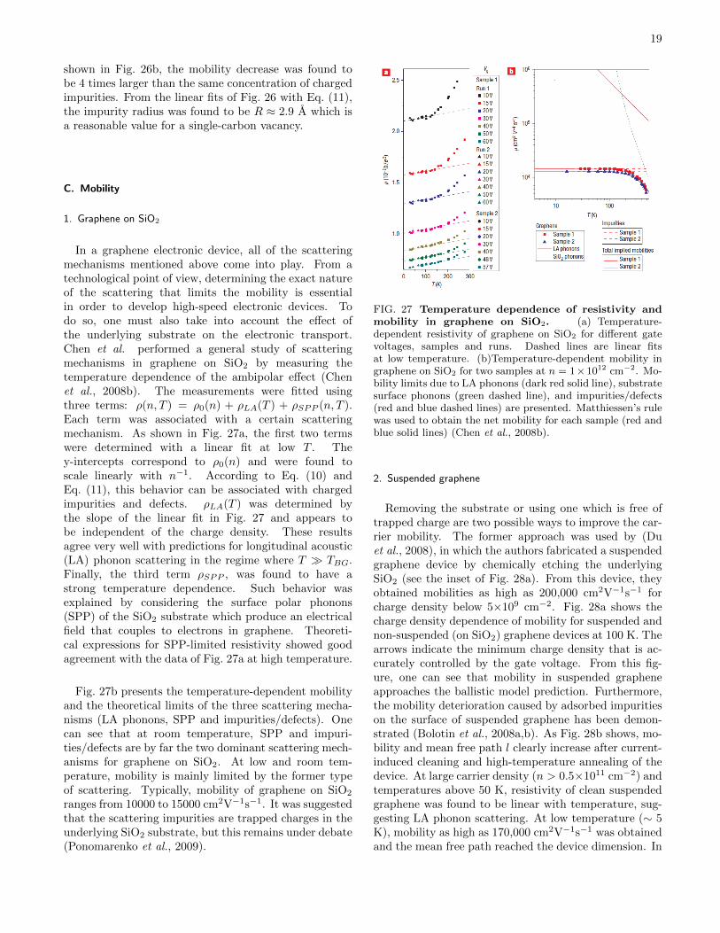
1. Graphene on SiO2
In a graphene electronic device, all of the scatteringmechanisms mentioned above come into play. From atechnological point of view, determining the exact natureof the scattering that limits the mobility is essentialin order to develop high-speed electronic devices. Todo so, one must also take into account the effect ofthe underlying substrate on the electronic transport.Chen et al. performed a general study of scatteringmechanisms in graphene on SiO2 by measuring thetemperature dependence of the ambipolar effect (Chenet al., 2008b). The measurements were fitted usingthree terms: ρ(n, T ) = ρ0(n) + ρLA(T ) + ρSPP (n, T ).Each term was associated with a certain scatteringmechanism. As shown in Fig. 27a, the first two termswere determined with a linear fit at low T . They-intercepts correspond to ρ0(n) and were found toscale linearly with n−1. According to Eq. (10) andEq. (11), this behavior can be associated with chargedimpurities and defects. ρLA(T ) was determined bythe slope of the linear fit in Fig. 27 and appears tobe independent of the charge density. These resultsagree very well with predictions for longitudinal acoustic(LA) phonon scattering in the regime where T TBG.Finally, the third term ρSPP , was found to have astrong temperature dependence. Such behavior wasexplained by considering the surface polar phonons(SPP) of the SiO2 substrate which produce an electricalfield that couples to electrons in graphene. Theoreti-cal expressions for SPP-limited resistivity showed goodagreement with the data of Fig. 27a at high temperature.
Fig. 27b presents the temperature-dependent mobilityand the theoretical limits of the three scattering mecha-nisms (LA phonons, SPP and impurities/defects). Onecan see that at room temperature, SPP and impuri-ties/defects are by far the two dominant scattering mech-anisms for graphene on SiO2. At low and room tem-perature, mobility is mainly limited by the former typeof scattering. Typically, mobility of graphene on SiO2
ranges from 10000 to 15000 cm2V−1s−1. It was suggestedthat the scattering impurities are trapped charges in theunderlying SiO2 substrate, but this remains under debate(Ponomarenko et al., 2009).
FIG. 27 Temperature dependence of resistivity andmobility in graphene on SiO2. (a) Temperature-dependent resistivity of graphene on SiO2 for different gatevoltages, samples and runs. Dashed lines are linear fitsat low temperature. (b)Temperature-dependent mobility ingraphene on SiO2 for two samples at n = 1×1012 cm−2. Mo-bility limits due to LA phonons (dark red solid line), substratesurface phonons (green dashed line), and impurities/defects(red and blue dashed lines) are presented. Matthiessen’s rulewas used to obtain the net mobility for each sample (red andblue solid lines) (Chen et al., 2008b).
2. Suspended graphene
Removing the substrate or using one which is free oftrapped charge are two possible ways to improve the car-rier mobility. The former approach was used by (Duet al., 2008), in which the authors fabricated a suspendedgraphene device by chemically etching the underlyingSiO2 (see the inset of Fig. 28a). From this device, theyobtained mobilities as high as 200,000 cm2V−1s−1 forcharge density below 5×109 cm−2. Fig. 28a shows thecharge density dependence of mobility for suspended andnon-suspended (on SiO2) graphene devices at 100 K. Thearrows indicate the minimum charge density that is ac-curately controlled by the gate voltage. From this fig-ure, one can see that mobility in suspended grapheneapproaches the ballistic model prediction. Furthermore,the mobility deterioration caused by adsorbed impuritieson the surface of suspended graphene has been demon-strated (Bolotin et al., 2008a,b). As Fig. 28b shows, mo-bility and mean free path l clearly increase after current-induced cleaning and high-temperature annealing of thedevice. At large carrier density (n > 0.5×1011 cm−2) andtemperatures above 50 K, resistivity of clean suspendedgraphene was found to be linear with temperature, sug-gesting LA phonon scattering. At low temperature (∼ 5K), mobility as high as 170,000 cm2V−1s−1 was obtainedand the mean free path reached the device dimension. In

20
FIG. 28 Conductance and mobility in suspendedgraphene as a function of charge density. (a) Mobilityvs. charge density for suspended (red line) and non-suspended(black line) graphene at T = 100 K. The blue line representsthe ballistic model prediction. Inset: schematic representa-tion of the suspended graphene device (Du et al., 2008). (b)Conductance vs. gate voltage (at T = 40 K) for a suspendedgraphene device before (blue line) and after (red line) anneal-ing and current-induced cleaning. The red dotted line wascalculated using a ballistic model. Inset: AFM image of thesuspended graphene device (Bolotin et al., 2008a).
these conditions, conductivity is well described by theballistic model as shown in Fig. 28b.
3. Other substrates
Although suspended graphene shows impressive trans-port properties, this geometry imposes evident con-straints on the device architecture. To overcome thisproblem, boron nitride (BN) was proposed as a sub-strate (Dean et al., 2010b). Compared to SiO2, BNhas an atomically smooth surface, is relatively free ofcharged impurities, has a lattice constant similar tothat of graphene and high surface phonon frequencies.All these advantages result in a mobility about threetimes higher than that of graphene on SiO2. However,
graphene/BN devices are troublesome to fabricate andare thus not ideal for industrial applications. Currently,large area graphene synthesized by CVD or thermal seg-regation is the most promising material for technologicalapplications since it can be produced on a wafer scale(Kim et al., 2009; Li et al., 2009). Depending on thetechnique, large scale graphene (on SiO2) typically showsmobilities lower than 5000 cm2V−1s−1 (Avouris, 2010).The scattering mechanisms responsible for this reducedmobility are still under investigation. Preliminary stud-ies suggested that grain boundaries (Yazyev and Louie,2010), doping defects (Wei et al., 2009) and ineffectivegate voltage control (Cao et al., 2010) might limit themobility. In addition to mobility, a common way to char-acterize the quality of large scale graphene is to measureits sheet resistance Rs (resistivity at Vg = 0). This prop-erty varies with the synthesizing technique used and canbe as low as 125 Ω/2 (Bae et al., 2010). It was also shownthat sheet resistance increases with decreasing tempera-ture (Park et al., 2010). This observation contrasts withthe metallic behavior (dσ/dT < 0) of pristine grapheneflakes but agrees with the insulating behavior of irradi-ated graphene (with defects) (Chen et al., 2009).
Substrate Production µ σmin Ref.
technique (×103 cm2V−1s−1) (e2/h)
SiO2/Si Exfoliation 10-15 4 a
Boron nitride Exfoliation 25-140 6 b
Suspended Exfoliation 120-200 1.7/π c
SiC Thermal-SiC 1-5 - d
SiO2/Si Ni-CVD 2-5 - e
SiO2/Si Cu-CVD 1-16 - f
TABLE III Mobility range (µ) and minimum con-ductivity (σmin) of graphene produced by differenttechniques and deposited on different substrates. a:(Novoselov et al., 2004), b: (Dean et al., 2010b), c: (Bolotinet al., 2008b), d: (Emtsev et al., 2009), e: (Kim et al., 2009),f: (Li et al., 2010b)
D. Minimum conductivity
The presence of disorder in graphene (ripples, defects,impurities, etc.) produces fluctuations in its electro-static potential. We mentioned above that these per-turbations are significant at the Dirac point where thescreening of the potential fluctuations is weak due tothe low charge density. These fluctuations in the chargedensity can be thought of as electron-hole puddles andhave been observed experimentally using scanning probemethods (Martin et al., 2008; Zhang et al., 2009a) ongraphene/SiO2 samples. Experimentally, these disor-dered graphene samples have a minimum conductivityabout π times larger than that predicted for ballistic

21
transport given in Eq. (6). This discrepancy betweentheory and experiments was observed in 2004 (Novoselovet al., 2004) and was known as “the mystery of the miss-ing pi.” The effect of doping on the minimum conductiv-ity was also investigated in a study of charged-impurityscattering (Chen et al., 2008a). It was found that σmindecreases on initial doping and reaches a minimum near4e2/h only for non-zero charged impurities. This sug-gests that charged impurities trapped in the SiO2 sub-strate, located at the graphene/SiO2 interface or on thegraphene surface are responsible for the minimum con-ductivity obtained experimentally.
To verify this conclusion, the minimum conductivityof clean suspended graphene was measured as a functionof temperature (Du et al., 2008). As Fig. 29a shows,minimum conductivity decreases with temperature andapproaches the ballistic prediction down to a factor of1.7. However, the linear temperature dependence wasnot expected. Another group also investigated the near-ballistic regime by measuring the minimum conductivityon samples with different aspect ratios (W/L) and surfaceareas at low temperature (∼1.5 K) (Miao et al., 2007).For large-area samples (∼3 µm2), the minimum conduc-tivity is mostly independent of the aspect ratio (inset ofFig. 29b). On the other hand, small-area devices (<0.2µm2) yield results that are clearly dependent on the as-pect ratio (Fig. 29b). Devices with wide electrodes andshort channels (large W/L) approach the theoretical min-imum conductivity in the ballistic regime. Table III com-pares the carrier mobility and minimum conductivity ofgraphene produced by different techniques and on differ-ent substrates.
E. Other transport properties
Concerning electronic applications, graphene has at-tracted considerable attention due to its high mobility.However, other transport properties must be taken intoaccount in order to develop graphene-based technologiessuccessfully. Among those properties, saturation velocityis particularly relevant for field-effect transistor (FET)applications. In modern FETs, short channel lengths re-sult in high electrical fields (Schwierz, 2010) of around∼100 kV/cm. In such conditions, the carriers acquireenough kinetic energy to excite the optical phonon modesof graphene (Avouris, 2010). As a consequence, carriervelocity saturates, reducing the relevance of mobility todevice performance. The optical phonons of graphenehave higher energy (∼160 meV) than those of commonsemiconductors such as Si (55 meV) (Dorgan et al., 2010).Consequently, the intrinsic saturation velocity is higherin graphene than in conventional semiconductors.
Numerical values of saturation velocity are presentedin Table II, and Fig. 30 shows the experimental and the-oretical dependence of saturation velocity on charge den-
FIG. 29 Minimum conductivity of graphene. (a) Mini-mum conductivity vs. temperature for a suspended graphenedevice. The upper dashed line represents the 4e2/h limit forgraphene with charged impurities. The lower dashed line cor-responds to the theoretical value in the ballistic regime (Duet al., 2008). (b) Minimum conductivity vs. aspect ratio forsmall and large (inset) graphene/SiO2 devices (Miao et al.,2007).
sity for graphene/SiO2. A simple phonon emission model(Meric et al., 2011) predicts that saturation velocity isproportional to 1/n1/2. In Fig. 30, the upper and lowertheoretical curves correspond to saturation velocities lim-ited by optical phonons of graphene and SiO2, respec-tively. The experimental results suggest that both kindsof phonons play a role in limiting νsat but that substratephonons of SiO2 are dominant for this device (Dorganet al., 2010). Some studies also point out that currentnever reaches a complete saturation in some graphene de-vices. This incomplete saturation might be due to a com-petition between disorder and optical phonon scattering(Barreiro et al., 2009), or the formation of a “pinch-off”region (Meric et al., 2011). Mechanisms limiting the sat-uration velocity are under active investigation.
Graphene has excellent transport properties, but totake advantage of them, carriers must be injected and col-lected through metal contacts. These electrical contacts

22
FIG. 30 Electron saturation velocity of graphene onSiO2. Electron saturation velocity vs. charge density for anelectric field of 2 V/µm at T = 80 K and 300 K. The upperand lower dashed curves correspond to theoretical saturationvelocities limited by optical phonons of graphene and SiO2,respectively (Dorgan et al., 2010).
produce energy barriers that limit the charge transfer atthe graphene/metal junction (Avouris, 2010). This limi-tation results in a contact resistance which can be mea-sured and should be reduced to create high-performancegraphene devices. One way to determine the contact re-sistance is to fabricate variable channel length devicesand to extrapolate the resistance to zero channel length.It was shown that contact resistance is temperature andgate voltage dependent, and that it varies from about100 Ω µm to a few kΩ µm (Xia et al., 2011). Finally,it is worth pointing out that graphene can sustain cur-rent densities greater than 108 A/cm2, which is 100 timeshigher than those supported by copper (Moser et al.,2007). Graphene can thus be used as interconnects inintegrated circuits.
Since Geim’s and Novoselov’s seminal work (Novoselovet al., 2004), graphene’s unique electronic properties haveattracted massive interest and created an explosion ofscientific activity. Much ink has been spilled about theambipolar field effect, the ultra-high mobility of grapheneand the limiting scattering mechanisms, as well as theminimum conductivity. In this section, we reported someof the main experimental studies on these ever growingsubjects. In the next section, we turn our attention tothe related but more specific topics of magnetotransportand quantum Hall effect in graphene.
VII. MAGNETORESISTANCE AND QUANTUM HALLEFFECT
The first demonstration, in the early 1980s, of the ex-istence of a so-called quantum Hall effect (QHE) of thetwo-dimensional electron gas (2DEG) at the interfacesof semiconductor heterostructures sparked great inter-est in the experimental study of the properties of low-dimensional systems (Klitzing et al., 1980). Thus it isperhaps no surprise that when the one atom thick, two-dimensional lattice of graphene could finally be isolatedin 2004, physicists immediately tried to characterize itsmagnetotransport properties, which are still an impor-tant field of research today. The purpose of this sec-tion is to recapitulate the present state of experimen-tal knowledge about magnetotransport measurements ingraphene. Firstly, we will describe the general experi-mental procedures that are necessary to carry such mea-surements. Secondly, we will briefly review the funda-mental physics relevant to localization phenomena and tothe QHE. Finally, we will show how these techniques pro-vide information on the electronic properties of graphenethrough weak (anti-)localization, the integer QHE andthe fractional quantum Hall effect (FQHE).
A. Experimental procedures
We first describe the basic experimental proceduresrequired to perform low temperature magnetotransportmeasurements in graphene.
1. Setup
The setup consists of a superconducting electromagnet(typically Nb based type-II superconductor, e.g. NbTi orNbSn3) immersed in a liquid helium cryostat. It is rep-resented in Fig. 31. Thus the sample can be refrigeratedto temperatures of 4 K and below. Lower temperaturesare achieved by reducing the vapor pressure of helium bypumping. Furthermore, in liquid helium the fields gener-ated in the electromagnet can reach high maximal valuestypically ranging between 6 and 14 T.
The sample is placed at the bottom of the cryostat insuch a way that the field is perpendicular to the planeof the graphene. The device is usually conceived for 4-terminal measurements, as illustrated in Fig. 32. A smallcurrent is driven through the end terminals and voltagemeasurements are carried out between different combina-tions of the lateral terminals. This avoids the measure-ment of the contact resistance at the current injectionpoints. The longitudinal resistivity ρxx is the ratio ofthe longitudinal voltage to the current normalized by theaspect ratio. The Hall resistivity ρxy and the Hall Re-sistance Rxy are identical and are defined as the ratio

23
FIG. 31 Setup for magnetotransport measurements.The cryostat is cooled to T = 4 K in two steps using liq-uid nitrogen and liquid helium. A solenoidal superconductingmagnet creates a magnetic field perpendicular to the plane ofthe graphene. The helium bath can be pumped on to yieldeven lower temperatures.
of the transverse voltage to the current. The Hall con-ductivity σxy is related to the resistivity by the inversetensor relation σxy =
ρxyρ2xy+ρ2xx
.
FIG. 32 Magnetotransport measurements. Top:Graphene is etched into a 4-terminal Hall bar. Gold electrodesare used to perform electrical measurements. The width ofthe central wire is 0.2 µm. Bottom: Graphene is placed ona thin SiO2 layer (285-300 nm), which is itself on a dopedSi wafer. A gate voltage Vg allows the carrier density to betuned. Figure from (Novoselov et al., 2005).
2. Carrier density tuning
In graphene, the carrier density n can be tuned us-ing the electric field effect, as discussed in Sec. VI. A
graphene sheet is placed on a SiO2 substrate about 330nm thick, which in turn lies on a doped Si wafer. A gatevoltage is applied on the Si to inject electron carriers inthe graphene or withdraw them. In the latter case, holescarry the current. Thus graphene can be studied aboveand below the neutral point corresponding to the Fermienergy and for which in principle n = 0.
The calibration is done using the conventional Hall ef-fect. In a (low) applied magnetic field, the Hall resis-tance is related to the current by Rxy = RHBI, whereRH = 1
nq is the Hall constant and q is the charge of the
carriers. A measurement of 1RH
for different gate volt-ages Vg allows one to establish a linear map between thecarrier density n and Vg for both holes and electrons. Anexample of calibration is shown on Fig. 33.
FIG. 33 Measurement of the conventional Hall effectfor different gate voltages Vg gives Vg ∝ n. The Hall constantRH is related to the carrier density by RH = − 1
ne. Figure
from (Novoselov et al., 2005).
3. Observation of the quantum Hall effect
The observation of the QHE is conditional on manyfactors.
1. High quality samples must be used in order to max-imize the momentum scattering time τq of the elec-trons.
2. High magnetic fields B are required in order forthe cyclotron period of the carriers to be muchshorter than the scattering time τq. Equivalently,this means that the cyclotron frequency ωc of anelectron must be much higher than the broadeningof the carrier energy levels (the Landau levels, seeSec. VII.B): ωcτq 1.
3. Low temperatures are needed in order for the ther-mal energy kBT to be much less than the spacinghωc of the Landau levels: kBT << hωc.

24
In graphene, the integer QHE can be observed at liq-uid helium temperature for fields ranging from about 1T and higher. For high magnetic fields the effect can beobserved for much higher temperatures (Novoselov et al.,2005). As an extreme example it has been shown that fora gigantic field of B = 45 T, the QHE remains detectableat room temperature (Novoselov et al., 2007). The obser-vation of the FQHE requires much more extreme condi-tions. The FQHE can be observed in graphene for fieldsabove 2 T for temperatures lower than 1 K and it can sub-sist up to T = 20 K at B = 12 T, provided that the sam-ple is ultraclean and that the graphene is suspended tosuppress scattering. This yields very low charge inhomo-geneity of order n = 109 cm−2 (Du et al., 2009). In suchsmall devices the contacts of the 4-terminal measure-ment prevent the appearance of the QHE and one mustperform a two-terminal measurement instead (Du et al.,2009). More recently, FQHE measurements in graphenehave been performed on graphene lying on a hexagonalboron-nitride substrate at fields of the order of B = 35T and temperatures of the order of T = 0.3 K (Deanet al., 2010a). Such fields cannot be reached with thesimple setup illustrated in Fig. 31. Instead, these mea-surements are performed in High Magnetic Field Labora-tories such as the National High Magnetic Field Labora-tory at Florida State University or Grenoble High Mag-netic Field Laboratory in France.
B. Theoretical background
1. Chiral electrons and pseudospin
Imagine a gas of electrons in the x-y plane confined bysome potential well in the z-direction. We assume thatthis well is deep and narrow enough, and hence that theenergy levels of the well are separated enough, so thatthe electrons are forbidden to access its excited statesthrough any excitations. Then we say that the electronmotion is two-dimensional.
At low carrier density n, the dispersion of graphene islinear around a Dirac point (call it K) so that we can-
not define an effective mass such that E = h2~k2
2m∗ as insemiconductor samples. Instead it can be shown that inthe continuum limit (i.e. taking the position of the elec-tron on the lattice to be a continuous variable), the mo-tion of the electron around a single Dirac point shouldbe described by the Dirac-Weyl equations for masslessfermions discussed in Sec. II using the Hamiltonian ofEq. (3) (Castro Neto et al., 2009):
(hvF~σ · ~k
)ΨK = EΨK , (12)
where ΨK is a spinor. It can be shown that the stateΨK acquires an extra phase (a Berry phase) of π on a
closed trajectory (Castro Neto et al., 2009). This is keyto understanding the weak localization measurements ingraphene discussed below.
Since in graphene there are two inequivalent Dirac val-leys K and K’ with the same dispersion, there is an equa-tion similar to Eq. (12) for K’. This leads to an extra val-ley degeneracy for the state of the electron and to chiralelectrons: the state ΨK in valley K has a different he-licity than a state ΨK′ in valley K’. We call the doublet(K, K’) the valley pseudospin. We conclude that the en-ergy levels should be 4 times degenerate: two times forthe pseudospin and two times for the actual spin of theelectron.
In a graphene bilayer, two sheets of graphene arestacked onto each other (in the natural Bernal stackingof graphite) (Castro Neto et al., 2009). In such a system,the carriers can hop between the layers and the dispersionrelation is not linear. Instead, the valence and conductionbands consist of two parabolic bands of the same curva-ture touching at the neutral point (Castro Neto et al.,2009). The theory of Eq. (12) can then be extended toshow that the carriers should be massive Dirac fermionswith a Berry phase of 2π (Novoselov et al., 2006).
2. Landau levels
Eq. (12) can be solved in the presence of a magneticfield and the result predicts a sequence of energy levelscalled the Landau levels (LL) (Apalkov and Chakraborty,2006; Castro Neto et al., 2009; Ezawa, 2008; Gusynin andSharapov, 2005):
EN = sgn(N)√
2ehv2F |N | N = 0,±1,±2... (13)
The energy is measured with respect to the Dirac point(i.e. the energy at the Dirac point is zero). Each suchlevel should also have the 4-fold degeneracy discussedabove. Note that in a semiconductor 2DEG, the LLswould be equally separated by an amount hωc where ωc =e|B|mc
is the cyclotron frequency and mc the cyclotron mass(Datta, 1997), which from Eq. (13) is clearly not the casefor graphene. We sketch a figure of the splitting of thebands in LLs for graphene in Fig. 34.
For bilayer graphene, we find a different expression:
EN = sgn(N)hωc√|N | (|N |+ 1) N = 0,±1,±2...
(14)
It can be shown that the extra layer degree of freedomshould give rise to an extra degeneracy for the levelN = 0and only for that level. Thus, the N = 0 level is 8 timesdegenerate while the others keep the 4-fold degeneracy ofgraphene. The splitting of the bands in LLs for bilayergraphene is illustrated schematically in Fig. 34.

25
FIG. 34 Schematic representation of the formation ofLandau levels in graphene (top) and bilayer graphene (bot-tom). In both cases the levels are not equally spaced and theneutral point has an associated LL. In graphene each level is4 times degenerate because of the spin and valley pseudospin.In bilayer graphene the lowest LL N = 0 is 8 times degeneratebecause of the extra layer degree of freedom.
C. Measurements of weak localization and antilocalizationin graphene
1. Quantum interferences
Quantum interferences have long been known to affecttransport measurements at low temperatures. In partic-ular, two-dimensional electron systems in the presenceof a (low) magnetic field show variations of conductancewith respect to the value in the absence of a field. Thiseffect is known as weak (anti-)localization.
Consider an electron hitting an impurity and goingback in the direction from which it came. In a classicalpicture, this could happen in a number of ways. In partic-ular, the electron could go around the impurity clockwiseor counter-clockwise (see Fig. 36). However, since elec-trons are quantum mechanical waves, we must add eachof the possible paths and make them interfere together toget the net probability of the electron to have backscat-tered. Electrons in conventional 2DEGs, in the absenceof spin-orbit interaction and scattering by magnetic im-purities, gain the same phase on both trajectories and in-terfere constructively, leading to an increased probabilityof backscattering compared to the value expected fromthe Drude model. We say that the electrons exhibit weaklocalization (WL). If a magnetic field is applied, an addi-tional (Aharonov-Bohm) phase is added between the twopaths, destructive interference occurs and the conduc-tance increases (positive magnetoconductance) (Tikho-nenko et al., 2009).
In graphene, however, it can be shown that becauseof the additional Berry phase of π of the wave func-tion, the two paths end up in opposite phase in the ab-sence of spin-orbit interaction and scattering within orbetween Dirac valleys. Therefore application of a mag-netic field can only restore the constructive interferenceand decrease the conductance (negative magnetoconduc-
tance) (Morozov et al., 2006; Tikhonenko et al., 2009).We say that the electrons exhibit weak anti-localization(WAL). Note that conventional electrons which couplestrongly through spin-orbit interactions can also exhibitWAL. However, this effect is not expected in graphenebecause of the small mass of the carbon atom (Tikho-nenko et al., 2009).
2. Measurements
The early quantum interference measurements ongraphene showed no WAL and a strongly suppressed WL.This was attributed to suppression of interference withinone Dirac valley due to ripples and large defects (Moro-zov et al., 2006). More recently, it was demonstrated thatboth WAL and WL could be observed in graphene un-der the proper conditions (Tikhonenko et al., 2009). Thebehavior of the magnetoconductance is shown on Fig. 35.
FIG. 35 Weak localization and anti-localization ingraphene. (a) The sample is studied for various carrier den-sities (here I, II and III). The QHE shows that the sample isindeed two-dimensional (see Sec. VII.D). The sample is an-nealed at T ≈ 400 K for 2 hours to increase its homogeneity.(b), (c) and (d) Variation of the magnetoresistance behavioras n and T are changed. A transition occurs between WL andWAL and negative magnetoconductance (WAL) is observedfor low n and high T due to the competition between valleyscattering and dephasing processes (see text). Figure from(Tikhonenko et al., 2009).
The data shows WAL (negative magnetoconductance)for both decreasing carrier density and increasing temper-ature. The increasing temperature reduces the dephasing

26
time τφ of the phase of the electron due to thermal fluc-tuations, while decreasing carrier density increases theintervalley and intravalley elastic scattering times τi andτ∗ defined in the theory of reference (McCann et al.,2006). The latter are roughly temperature independent.Thus it is observed that the dephasing time is not theonly parameter controlling weak localization behavior ingraphene. Instead, one must consider the ratios ri =
τφτi
and r∗ =τφτ∗
. When they are small, anti-localization oc-curs while when they are big, localization occurs. Notethat there exist combinations of these parameters forwhich the correction to the magnetoconductance is sup-pressed. This is shown in Fig. 36.
FIG. 36 Phase diagram for weak (anti-)localization ingraphene. (a) A schematic representation of interference be-tween electron paths. For graphene it is expected to be nat-urally destructive and a magnetic field is expected to partlyrestore constructive interference (see text). (b) A phase di-agram for weak localization behavior in graphene. It is seenthat the ratios of the dephasing time to the two valley scatter-ing times determine the magnetoresistance behavior. Figurefrom (Tikhonenko et al., 2009).
In graphene, the quantum corrections to the conduc-tance survive at much higher temperatures than for2DEG semiconductor structures because the electron-phonon scattering is expected to be weak in the system.Indeed, weak (anti-)localization can be observed up tomuch high temperatures in graphene, in particular inlarge scale CVD grown graphene (Whiteway et al., 2010).It turns out that electron-electron scattering could be re-sponsible for the disappearance of magnetoconductanceat high temperatures (Tikhonenko et al., 2009).
D. Measurements of the quantum Hall effect in graphene
Here we review the principal features of the QHE ingraphene and compare them to the conventional results.We first discuss the general features of the QHE.
1. Shubnikov-de Haas oscillations
The existence of LLs implies the appearance of the so-called Shubnikov-de Haas oscillations (SdHO) in the QHsystem. The SdHO consist of a strong modulation of thelongitudinal resistivity ρxx as a function of the carrierdensity n. The minima of these peaks correspond to acompletely vanishing longitudinal resistivity. This occurswhen the chemical potentials of both leads sit betweenthe LLs, as illustrated in Fig. 37. Then all the ~k carryingstates of the LLs are completely filled so that the elec-trons cannot carry current in a LL. The only states thatcarry current are the edge states at the Fermi level (seeFig. 37). Furthermore, the magnetic field is such thateach edge carries current in different directions. Hence,the only way for backscattering to occur is for an elec-tron to go from one edge to another, which is not feasible.Thus scattering is suppressed and no voltage can buildup, hence ρxx vanishes. As the Fermi level is raised, aLL may sit at the chemical potential of the leads, whichallows for some backscattering, hence producing a maxi-mum in resistivity.
FIG. 37 Quantization of Hall conductance ingraphene. (a) The density of states is peaked at the LLsand broadened by the presence of disorder. (b) Edge statestopologically separated by the magnetic field conduct the cur-rent between the leads at fixed potential. In the absence ofscattering, the quantum of conductance e2/h carried by eachchannel translates into the quantization of the Hall conduc-tivity σxy (see text).
2. Conductance quantization
Associated with the SdHO is the celebrated phe-nomenon of Hall conductance quantization. It is ob-served that at the values of n for which the zeros in ρxxoccur, the Hall resistivity ρxy is constant and forms aplateau that is a multiple ν−1 of h/e2. The integer ν issaid to be the filling factor of the QH state and repre-sents the total number of levels below the Fermi energy.In fact, there are as many conducting edge channels as

27
there are filled levels, and one can show that each suchchannel should contribute one quantum of conductancee2
h (Datta, 1997). In the absence of backscattering, oneexpects each edge to be at the same potential as the leadthat provides its carriers: this implies that the transverseHall voltage is the same as the potential difference be-tween the leads. Therefore the Hall conductance shouldbe the same as the sum of the conductance of each ofthese ν channels. Thus:
ν =Gxy
(e2/h)(15)
This phenomenon is known as the quantum Hall effect.The reader is referred to (Datta, 1997) for a thorough the-oretical treatment of ballistic transport in micron scalesamples.
3. Integer quantum Hall effect
a. Monolayer graphene For the plateaus of the conven-tional QHE in semiconductor heterostructures, ν is apositive integer and a finite number of charge carriers isrequired to occupy the lowest LL. At low magnetic field,only the even filling factors appear because the LLs canbe filled with both spin up and spin down electrons. Wehave the sequence:
ν = 2, 4, 6, 8, 10... (16)
Therefore the sequence of ν’s provide information onthe degeneracies of the electron states or equivalently, ontheir symmetries. If the magnetic field is increased, thedegeneracies can be completely lifted via Zeeman inter-action of the spin with the magnetic field, revealing theentire sequence of filling factors.
FIG. 38 Typical measurement of the integer quantumHall effect. The Hall resistivity exhibits plateaus quantizedin exact multiples of h
e2. Image created by D.R. Leadley,
Warwick University (1997).
As a two-dimensional system, graphene is expected toexhibit the QHE. It was observed in 2005 by two research
groups (Novoselov et al., 2005; Zhang et al., 2005) andshowed features that were characteristic of the linear dis-persion of graphene. A measurement of the conventionalQHE in graphene is shown in Fig. 39.
FIG. 39 Integer quantum Hall effect in graphene. Thecarrier density n can be tuned across the neutral point n = 0.The absence of a plateau at n = 0 indicates the presence ofa LL at the neutral point. The inset shows bilayer graphene,discussed in Sec. VII.D.3.b. Figure from (Novoselov et al.,2005).
The sequence of observed plateaus is very differentfrom that of the conventional QHE. The precise sequenceis:
ν = ±2,±6,±10... (17)
We notice that the carrier density (i.e. the Fermi level)of graphene can be tuned through both the valence andconduction band of graphene, resulting in negative ν forholes and positive ν for electrons. From the sequencewe immediately see that each plateau contributes 4e2/hto the conductance, instead of 2e2/h. This is indicativeof the expected extra valley degeneracy of the states, inaddition to the spin degeneracy. Another interesting fea-ture of this sequence is that there is no plateau at zerocarrier density. Thus there is a LL N = 0 at the neutralpoint with degenerate holes and electrons as seen fromEq. (13). The structure of electron and hole states is alsocompletely symmetric.
Fig. 40 shows a complete lift of the degeneracy of theN = 0 LL at ultrahigh magnetic fields, confirming explic-itly the 4-fold degeneracy of the level (Zhang et al., 2006).The Zeeman coupling in graphene is too weak to causethe lifting of the spin degeneracy and does not explainthe breaking of the valley pseudospin symmetry (Zhanget al., 2006, 2005). Instead, the lifting of the degeneraciesis suspected to be caused by enhancement of Coulomband exchange interactions in the sample. This is due tothe fact that as the field is increased the cyclotron or-bits become smaller and the carriers come closer to each

28
other (Dean et al., 2010a; Ezawa, 2008). All integer fill-ing fractions can be observed for the cleanest samples(Dean et al., 2010a).
FIG. 40 Complete lifting of the degeneracy of the low-est LL with fields from 9 T (circle) up to 45 T (star). Theexpected 4-fold degeneracy is shown explicitly by the presenceof plateaus at ν = 0 and ν = ±1. The plateaus at ν = ±4show partial degeneracy lifting of the levels N = ±1. All de-generacies can be lifted in clean samples, see Fig. 44. Figurefrom (Zhang et al., 2006).
Just like the conductance quantization, the SdHO os-cillations show unusual behavior. We still observe theirminima at the positions of the plateaus, as seen in Fig. 39.
FIG. 41 Determination of the dispersion of graphenethrough SdHO oscillations. (a) The SdHO decay morerapidly with temperature as the carrier density is increased.The data can be fitted to yield the cyclotron massmc. (b) Thecyclotron mass varies with carrier density as
√n, implying the
linear dispersion of graphene. Figure from (Novoselov et al.,2005).
However, their amplitude decays more rapidly withtemperature as the density n is increased. Theoreticalstudies have shown that for a given n, the amplitude Aof the SdHO should follow (Castro Neto et al., 2009):
A ∝ T
sinh 2π2TkBmcheB
(18)
where mc is the cyclotron mass of the electrons at theFermi level (Novoselov et al., 2005).
A fit to the data shows that the rapid decay of theSdHO implies that mc ∝
√n, as shown in Fig. 41. Unlike
in semiconductor devices, the cyclotron mass in graphenevaries with density. It is possible to show that this depen-dence of mc on n implies the linear dispersion of grapheneE(k) = hvF k and thus the form of the LLs given inEq. (13) (Novoselov et al., 2005).
b. Bilayer graphene The quantum Hall effect can also beobserved in multilayer graphene. The inset of Fig. 39 aswell as Fig. 42 shows measurements carried out on thegraphene bilayer (Novoselov et al., 2006). The observedsequence is as follows:
ν = ±4,±8,±12,±16... (19)
FIG. 42 Quantum Hall effect in bilayer graphene. As inthe case of the monolayer, the quantum Hall effect in graphenebilayer shows no plateau at ν = 0, indicating the presence of aLL at zero carrier density and the relativistic behavior of thebilayer. However, contrarily to the monolayer, the N = 0 levelis 8-fold degenerate as the height of the step indicates. Thisis consistent with the theoretical prediction of a “parabolicDirac point” at ν = 0, i.e. massive Dirac fermions. Figurefrom (Novoselov et al., 2006).
The absence of a plateau at ν = 0 is a common char-acteristic of the QHE in graphene and bilayer graphene.Once again it indicates the presence of a LL at zero en-ergy. However, this level is eight times degenerate as canbe seen from the 8e2/h jump in the Hall conductivity.The other levels keep the 4-fold degeneracy of graphene.This is what we expect from the additional layer degreeof freedom of the electron for a given spin and valley(Ezawa, 2008; Novoselov et al., 2006). The degeneracyof the lowest LL can be completely lifted by many-bodyinteractions in ultra-high magnetic fields (Zhao et al.,2010), as shown in Fig. 43.

29
FIG. 43 The degeneracy of the lowest LL of bilayergraphene is lifted by magnetic fields ranging from 9T to 35 T. We clearly distinguish for levels above the neutralpoint and 4 others start to be visible below the neutral points,accounting for the expected 8-fold degeneracy of this level.Figure from (Zhao et al., 2010).
4. Fractional quantum Hall effect
The extreme two-dimensional confinement in grapheneis expected to enhance many-body interactions betweenelectrons. Since 1982, we know that these interactionscan manifest through the so called fractional quantumHall effect (FQHE), consisting of the appearance of Hallplateaus at fractional (rational) values of the filling factorν (Tsui et al., 1982). The efforts to observe the FQHE ingraphene were without success for a long time because ofthe existence of a competing insulating state induced bydisorder near the neutral point ν = 0. The improvementsin the sample fabrication made its observation possiblein recent years.
FQH states can be understood as the realization of theinteger QHE for weakly interacting quasiparticles calledcomposite fermions. In a heuristic picture, an even num-ber of magnetic flux vortices bind with an electron toform an object with reduced effective charge that is afraction of the elementary charge e (Dean et al., 2010a;Jain, 1989). In graphene, the multiple components of theelectron wave function are expected to give rise to new in-teracting ground states with various spatial arrangementsof pseudospin (textures) that depend on the symmetriesof the states. These special states are theoretically pre-dicted to occur at filling factors that are multiples of 1
m ,where m is an odd integer (Ezawa, 2008). The FQHE al-lows for a characterization of these symmetries and putshard constraints on theoretical models. Different sym-metry scenarios are presented in Fig. 45.
FIG. 44 The FQHE in graphene. Multiple plateaus atrational filling factors show that electron interactions give riseto new states. Figure from (Dean et al., 2010a).
FIG. 45 Schematic SdHO structures correspondingto different possible symmetries of the lowest LL ingraphene. (a) Total symmetry breaking. (b) Either the spinor the valley symmetry is broken. (c) Full symmetry of thespin and valley degrees of freedom. The latter is the best fitto the observations. Figure from (Dean et al., 2010a).
Fig. 44 shows a clean and recent 6-terminal measure-ment of the FQHE in graphene made on a hexagonalboron-nitride substrate at ultrahigh fields (Dean et al.,2010a). The filling factors appear in the following se-quence:
ν = ±1
3,±2
3,±1,±4
3,±2,
7
3,
8
3, 3,
10
3,
11
3, 4,
13
3... (20)
The measurements for hole carriers were not performedfor ν < −2. The filling factors are all multiples of 1
3 , al-though 5
3 is missing. Furthermore, a peak in the SdHOmay indicate the emergence of a plateau at ν = 8
5 . Theeffect is much more robust under increase in tempera-ture than its counterpart in semiconducting devices, re-vealing the suspected enhancement of electron-electroninteractions in graphene compared to those occurring in2DEGs (Dean et al., 2010a; Du et al., 2009). The absenceν = ± 5
3 and the presence of ν = ± 13 is consistent with a
global SU(4) symmetry of the FQH state in the lowestLL (Dean et al., 2010a).
Previous measurements have been performed on verysmall (≤2 µm) 2-terminal ultraclean samples of sus-pended graphene (Bolotin et al., 2009; Du et al., 2009).For a discussion of the properties of suspended graphenesee Sec. VI.C.2. Their results are presented in Fig. 46.They also obtain the FQHE in the lowest LL at ν = 1
3and ν = 2
3 . While 2-terminal measurements make the

30
results less precise and harder to interpret (for example,the contact resistance makes it very hard to extract in-formation from the longitudinal resistance data and mayproduce unusual features at ν = 1
2 ), they possess the ad-vantage of being realizable with lower field magnets instandard physics laboratories.
FIG. 46 High quality suspended graphene samplesused by Bolotin et al. (left) and Du et al. (right). Thecontacts are less than 2 µm apart in both cases, making a 4-terminal measurement impossible. However, the FQHE canbe observed clearly at relatively low fields ranging from 5 Tto 12 T. Figures from (Bolotin et al., 2009; Du et al., 2009).
The observation of the anomalous quantum Hall effect,including its fractional daughter are one of the brightesthighlights, which propelled graphene as one of the moststudied materials in recent years. We now move awayfrom magneto-transport to discuss the mechanical prop-erties in the next section, which are very important forfuture applications in nanodevices.
VIII. MECHANICAL PROPERTIES
Microelectromechanical systems (MEMS) have beendeployed to perform common tasks such as opening andclosing valves, regulating electric current, or turning mir-rors. This is realized by employing microscopic machinessuch as beams, cantilevers, gears and membranes. TheseMEMS are found in many commercially available prod-ucts from accelerometers found in air bag deploymentsystems, gyroscopes in car electronics for stability con-trol and ink jet printer nozzles (Craighead, 2000). Thenanoscopic version of MEMS, nanoelectromechanical sys-tems (NEMS), demonstrate their own advantages in en-gineering and fundamental science in areas such as mass,force and charge detection (Ekinci and Roukes, 2005).All these electromechanical devices are functional onlyin response to an external applied force. The utmostlimit would be a one atom thick resonator. Robustness,stiffness and stability is thus important when reachingthis limit (Bunch et al., 2007).
The fabrication of graphene-based mechanical res-onators is still under active development. Presented hereis an overview of experimental results for single and mul-tilayer graphene sheets placed over predefined trenches.A simple drive and detection system is used to probethe mechanical properties of these graphene resonatorsin order to extract the fundamental resonance frequency.
This allows us to characterize the quality factor, Young’smodulus and built-in tension (Bunch et al., 2007). Onecan also extract this information from a separate ex-periment using an atomic force microscope (AFM) tip(Frank et al., 2007). In addition to their use as mechani-cal resonators, graphene sheets are robust (impermeable)enough to act as a thin membrane between two dissimilarenvironments (Bunch et al., 2008).
A. Overview of the harmonic oscillator
In order to study the mechanical properties ofgraphene and graphite sheets, one needs to comprehendthe basics of a harmonic oscillator. A classic example isa mass attached to a spring. In an ideal situation, thespring obeys Hooke’s law, but for large displacements,the spring does not follow Hooke’s law as the system issubject to damping, denoted by γ, which dissipates thevibrational energy of the system. In addition, a drivingforce F with frequency ω is necessary to drive oscillationsto the system. Therefore, the equation of motion for adamped harmonic oscillator is given by:
md2x
dt2+ γ
dx
dt+mω2
0x = F cos(ωt). (21)
The general solution is given by:
x = A cos(ωt− θ) (22)
where θ is the phase shift, the amplitude
A =F
mω20
Q√Q2(1− ω2
ω20)2 + ( ωω0
)2, (23)
and the quality factor
Q =mω0
γ. (24)
For a given peak with resonance frequency ω0 = 2πf0,the peak amplitude is QF/mω2
0 and its full-width halfmaximum (FWHM) determines the Q factor, given byf0/Q.
B. Tuning resonance frequency by electrical actuation
The mechanical resonators are exfoliated graphenesheets that are suspended over trenches on SiO2/Si sub-strates. These micron-sized sheets are doubly-clampedbeams which are secured to the SiO2 surface via van derWaals forces. A gold electrode defined by photolithogra-phy is used to electrically actuate the graphene resonator,

31
FIG. 47 Schematic of a suspended graphene resonatorfor electrical actuation (Bunch et al., 2007).
filling the role of the driving force F from Eq. (21). Allresonator measurements are performed in ultra-high vac-uum at room temperature. The actuation is an appliedalternating electric field used to drive the resonant mo-tion of the beam. A capacitor is then formed betweenthe bottom gate electrode and the contacted graphene,shown in Fig. 47. A voltage Vg applied to the capacitorinduces electric charges onto the beam. A small time-varying radio frequency (RF) voltage δVg at frequencyf is used to electrically modulate the beam on top of aconstant DC voltage (Bunch et al., 2007):
Vg = V DCg + δVg. (25)
The resulting electrostatic force is then given by:
Fel =1
2
dCgdz
V 2g ≈
1
2
dCgdz
(V DCg )2 +dCgdz
VgδVg (26)
where z is the distance between the graphene and thegate electrode.
The response due to a varying RF voltage is monitoredby a 632 nm He-Ne laser focused on the resonator. Asa result, the light creates an interference between thesuspended graphene sheets and the silicon back plane.Variations of the reflected light intensity are monitoredby a photodiode.
Plugging Eq. (26) into Eq. (23), one can speculate onthe behavior of the resonant peak as a function of appliedvoltage. The data for a few-layer graphene stack is shownin Fig. 48 for electrical drive on resonance. One can seethat the amplitude and frequency increase linearly withδVg at a fixed V DCg for the higher mode (Fig. 48B) whilethe frequency of the fundamental mode (Fig. 48A) doesnot change significantly. In addition, if Vg is increasedwhile δVg is fixed (Fig. 48C), both the amplitude of thefundamental mode and that of the higher mode increaselinearly as expected from Eq. (23). As for the frequency(Fig. 48D), it seems that there is evidence of positivetuning for the higher mode but that the fundamental
mode remains unaffected. A possible explanation for thetuning may originate from an electrostatic attraction tothe gate which increases the tension from stretching thegraphene.
FIG. 48 Resonance spectrum taken with an electro-static drive. Plot of the amplitude versus frequency of the(a) fundamental mode at 10 MHz and (b) the higher mode at35 MHz with increasing δVg while V DC
g remains fixed. Inset:Plot of the resonant peak amplitude with increasing δVg. De-pendence of the (c) amplitude and (d) frequency as functionof V DC
g at fixed δVg where the solid squares and triangles rep-resent the fundamental and higher mode respectively (Bunchet al., 2007).
C. Resonance spectrum by optical actuation
Another technique to actuate vibrations in resonatorsis an optical drive. A diode laser is shined on thesuspended graphene in which the graphene actuatesby itself via thermal expansion and contraction. Thismotion is controlled by the intensity of the diode laserset to a frequency f . This is then monitored by aphotodiode using a He-Ne laser through the proceduregiven in the previous section (Bunch et al., 2007).
Fig. 49A shows the resonance spectrum of a few-layergraphene sheet suspended over a SiO2 trench. Severalresonant peaks were measured; the first peak is thefundamental vibrational mode which will be the mainfocus of the discussion. The fundamental peak is themost pronounced peak, so it is easy to obtain themechanical characteristics of the resonator. Analyzinghigher modes is unnecessary as they depend on thefundamental frequency f0. The most appropriate fit toextract the resonance frequency f0 is a Lorentzian fit,giving f0 to be 42 MHz with a quality factor Q = 210.Fig. 49B shows similar results for a single layer graphene,

32
FIG. 49 Plots showing the resonance spectrum ofgraphene and graphite resonators. (a) Resonance spec-trum showing the fundamental mode and higher modes fora 15 nm thick multilayer graphene sheet taken with opticaldrive. Inset: Optical image of the resonator. Scale bar = 5µm. (b) Amplitude vs. frequency for a single layer graphene.The red curve represents the Lorentzian fit of the data (Bunchet al., 2007).
f0 = 70.5 MHz and Q = 78. The same measurementswere repeated for 33 resonators of different geometrieswith thicknesses ranging from 1 atomic layer to 75 nm.They are plotted in Fig. 50. The data shows that thefundamental frequency f0 largely varies from 1 MHzto 166 MHz with quality factors ranging between 20and 850. Knowing the fundamental resonance f0, thefollowing equation for a doubly-clamped geometry isused as a reference to extract the Young’s modulus ofthe sheets (Weaver et al., 1990):
f0 =
√√√√(A√E
ρ
t
L2
)2
+0.57A2S
ρL2t, (27)
where E is Young’s modulus, S is the tension perwidth, ρ is the mass density, t and L are the thickness andlength of the suspended graphene sheet, and A is a ge-ometrical constant; A = 1.03 for doubly-clamped beamsand 0.162 for cantilevers. The parameter S represents thebuilt-in tension on the graphene sheet which may comefrom the fabrication process or from the van der Waalsinteraction between the substrate and graphene. Assum-ing that the tension is sufficiently small, Eq. (27) pre-dicts that the fundamental frequency f0 scales as t/L2.Fig. 50A is a plot of the resonance frequency for res-onators with t > 7 nm (solid squares) and t < 7 nm (hol-low squares) as a function of t/L2 and the slope gives theYoung’s modulus E. Taken the density for bulk graphiteas ρ = 2200 kg/m3, the Young’s modulus of the graphenesheets plotted as dashed lines correspond to values be-tween 0.5 and 2 TPa. These values correspond well tothe Young’s modulus of 1 TPa of bulk graphite (Kelly,1981). This is the highest modulus resonator to date.This is in stark contrast to the 12-300 nm thick Si can-tilevers (Sazonova et al., 2004) which achieve values rang-ing between 53 - 170 GPa, and which are plotted as solid
triangles in Fig. 50A. For graphene resonators with t < 7nm, the data points are not as linear as for the thick res-onators. To elucidate these results, Scharfenberg et al.studied the elasticity effect of thin and thick graphenesamples on a corrugated elastic substrate such as poly-dimethylsiloxane (PDMS). For thin graphene samples, itadheres fully to the substrate so that the graphene followsthe topography of the substrate. As for thicker samples,it flattens the corrugated substrate. These observationssuggest that thin graphene flakes, despite their size, arehighly sensitive to tension, making them easier to deformthan the thicker samples (Scharfenberg et al., 2011).
FIG. 50 Measurements of the Young’s modulus and Qfactor for doubly-clamped beams. (a) Plot showing thefrequency of the fundamental mode of all the doubly-clampedbeams and Si cantilevers versus t/L2. The cantilevers areshown as solid triangles. The doubly clamped beams witht > 7 nm are indicated as solid squares while those witht < 7 nm are shown as hollow squares. The solid line is thetheoretical prediction with no tension. (b) Plot of the qualityfactor as a function of the thickness for all resonators (Bunchet al., 2007).
The quality factor is an important parameter to con-sider when dealing with resonators. It gives a good indi-cation of the resonator’s sensitivity to external perturba-tions. A high Q is thus essential for most applications. Aplot of Q as a function of the thickness for all grapheneresonators is shown in Fig. 50B. It seems that there isno clear dependence of quality factor on resonator thick-ness observed and the Q factor is on the order of hun-dreds. These Q factors are lower than diamond NEMS(Q'2500-3000) (Sekaric et al., 2002) and significantlylower than high tensile Si3N4 (Q'200,000) (Verbridgeet al., 2006). Thicker variants of graphene, like grapheneoxide (Q'4000) (Robinson et al., 2008b) and multilayerepitaxially grown graphene (Q'1000) (Shivaraman et al.,2009) have shown higher quality factors. Despite the us-ability of graphene as a mechanical resonator, the sourceof dissipation is still poorly understood. Recent progresson graphene resonators suspended over circular holes onSiNx membranes have shown some improvements on theQ factor. Thus, Fig. 51 demonstrates a clear dependenceof quality factor on the resonator diameter. The highestQ factor is about 2400 for a resonator with a diameter of22.5 µm (Barton et al., 2011).

33
FIG. 51 Resonance frequency and Q factor ofgraphene membranes. (a) Fundamental frequency f asa function of diameter D for 29 graphene membranes. Thered line is a fit of the data in which f ∼ D−0.9±0.1. (b)Quality factor of membranes as a function of diameter. Inset:the highest Q factor peak observed fitted with a Lorentzianindicating a value of 2400 (Barton et al., 2011).
D. Measurements by atomic force microscopy
In the previous subsections, the Young’s modulus ismeasured by considering the tension being small, neglect-ing the second term in Eq. (27) for a doubly-clampedbeam. The built-in tension in the suspended graphenemay indeed play a role in the mechanical measurements,a plausible explanation to the scattered data found inFig. 50 for thin graphene resonators. To measure thebuilt-in tension, an AFM tip with a calibrated springconstant is pressed onto the suspended graphene (Franket al., 2007). The spring constants on the sheet arethen extracted to calculate the Young’s modulus andbuilt-in tension. With an applied static force for adoubly-clamped beam and employing the relation f0 =(1/2π)
√ks/m and Eq. (27), the resulting effective spring
constant is:
ks = 16.23Ew
(t
L
)3
+ 4.93T
L. (28)
where w is the width of the sheet.
FIG. 52 Schematic of a deflected AFM tip while push-ing on the suspended graphene. ηgraphene is the heightthat the tip is deflected by the graphene and ∆zgraphene isthe height pushed by the tip (Frank et al., 2007).
Fig. 52 shows the schematic of an AFM tip pushingdown the suspended graphene sheet. The deflection of
the tip then helps to find the effective spring constant ofthe suspended sheet. The chosen AFM tip has a springconstant 2 N/m which enables the graphene to be de-flected by a detectable amount. The tip is pushed slowlyagainst the sheet and the relation between tip displace-ment and the position of the piezo is then plotted inFig. 53. As the AFM tip comes into contact with thesuspended graphene, the cantilever is pulled down ontothe surface resulting in a dip in the deflection as observedin Fig. 53a. From the tip’s spring constant, a graph of theforce exerted on the tip versus the displacement of thegraphene sheets can be extracted as plotted in Fig. 53b.The displacement can be written as:
zpiezo = ηgraphene + ∆zgraphene (29)
where ηgraphene is the deflection of the tip, zpiezo isthe location of the piezo moving the tip, and ∆zgrapheneis the deflection of the graphene sheet. From Hooke’slaw, the slope yields the effective spring constant of thesuspended graphene sheet.
FIG. 53 Measurement of the graphene’s spring con-stant. (a) Curve obtained from the deflection of the AFMtip by pushing down the suspended graphene sheet. The rightaxis represents the force corresponding to the tip displace-ment. (b) Plot of the force as a function of the displacementof the graphene sheet (Frank et al., 2007).
Fig. 54 shows the plot of the spring constant as afunction of the dimensions of the suspended graphenesheet for eight samples. The spring constant variesbetween 1-5 N/m. A linear fit is then used to extract thebuilt-in tension and Young’s modulus of the suspendedgraphene sheets. From Eq. (28), the slope suggests thata Young’s modulus E of 0.5 TPa, in good agreementwith suspended graphene actuated optically and bulkgraphite. The offset of the linear fit gives a tensionof 300 nN, suggesting that the built-in tension of allsuspended graphene sheets are on the order of nN.
Other work on AFM nanoindentation was realized ongraphene suspended over micron-sized circular wells toinvestigate the elasticity properties of graphene. Indent-ing defect-free graphene with an AFM tip similar toFig. 52, one can probe the elastic stress-strain response.

34
FIG. 54 Plot of the spring constant in the center ofthe suspended region versus w(t/L)3 for eight differentsamples with various thicknesses. The linear fit providesinformation about the built-in tension and Young’s modulusof the graphene sheets (Frank et al., 2007).
A non-linear elastic response model is fitted to find thatthe stiffness is about 340 N/m with intrinsic breakingstrength of 42 N/m (Lee et al., 2008).
As discussed in this section, graphene as an ultra-thinmembrane with extremely high bulk modulus is verypromising for potential applications in mechanical sys-tems, if the source of dissipation can be reduced sub-stantially, which should lead to a significant increase inQ factor. We now turn to applications of graphene astransistors.
IX. GRAPHENE TRANSISTORS
This section provides an overview of current experi-mental work being pursued toward the development ofgraphene field effect transistors (GFET). The two mostcommon varieties of transistor are the logic transistorand the analog transistor. The former is characterized,among other things, by a high Ion/Ioff ratio to ensurelow energy consumption (of the off state) and to main-tain a high logic interpretation yield. The latter is char-acterized primarily by its cutoff frequency, and is oftenused in high frequency applications as an amplifier. Bothtypes of devices, as we shall see, could benefit from theremarkable electrical properties of graphene.
A. Logic transistors
For more than forty years CMOS technology has dom-inated the logic transistor industry with the fabricationof MOSFETs. A general trend over the years has beento reduce the length of the transistor’s gate in order toachieve higher transistor densities but also increased per-formance produced by the higher electrical fields in thechannel region. However, as the size of the device is re-
duced, more and more issues (commonly known as shortchannel effects) begin to appear (Frank et al., 2001).These issues include but are not limited to such prob-lems as hot electron effects, velocity saturation effects,and punchthrough effects. It has been suggested thatgraphene, due to its monoatomic thickness, would reducethese parasitic effects (Schwierz, 2010). Graphene couldbe included in the channel region of transistors and thusprovide a high mobility channel which would help to re-duce the effect of short channel effects. One problem isthat graphene does not possess a bandgap since the con-duction and valence bands touch at the Dirac point. Thisreduces the on-off ratio of the transistor by several ordersof magnitude, such that a graphene FET will typicallyhave an on-off ratio < 10. This ratio is unacceptableif one wants to replace CMOS technologies where ratios> 107 are commonly achieved. It has been proposedby the International Technology Roadmap of Semicon-ductors (ITRS) that a ratio of 104 would be requiredfor logic applications. Such a ratio could be achieved ingraphene only by opening a bandgap at the Dirac point inorder to suppress the band-to-band tunneling (Fiori andIannaccone, 2009). A bandgap of 0.4 eV could achievethe desired on-off ratio (Schwierz, 2010). Several tech-niques are being envisioned for engineering a graphenebandgap. The following sections provide an overview ofthese methods.
1. Bilayer graphene
The first technique that we shall investigate is the useof bilayer graphene. Theoretical calculations have pre-dicted the possibility of a bandgap opening in this con-figuration (McCann, 2006). Such a structure allows theopening of a bandgap by breaking the symmetry of thebilayer stack (Bernal stacking) with the application of atransverse electrical field. One of the first investigationsof this approach is given in reference (Ohta et al., 2006).The authors used bilayer graphene on a SiC substrate.In such a structure, light doping is provided to the bot-tom graphene layer by the substrate and further dopingcan be introduced to the top graphene layer by the ad-sorption of potassium atoms. This setup was designedand fabricated to facilitate band structure analysis usingthe ARPES technique. Fig. 55 presents the experimentalband structure for increasing amounts of potassium dop-ing and a comparison to theoretical calculations. Onemay notice the good agreement between probed and the-oretical bandstructure. A maximal bandgap of approxi-mately 0.2 eV is observed using this technique.
The results presented above show the potential of bi-layer graphene for bandgap engineering. Several groupsused this material for designing FET devices (Oostingaet al., 2008). In these devices doping is induced usingthe field effect instead of using potassium atoms. Fig. 56

35
FIG. 55 Bandgap evolution as a function of the potas-sium doping. The doping level is controlled using the potas-sium adsorption of bilayer graphene. Shown from left to rightis a diagram of the evolution of the bandgap for an increasingdoping level per unit cell (Ohta et al., 2006).
presents a schematic representation of such a device. Thedouble gate configuration allows one to control both theFermi position and the bandgap size.
FIG. 56 Schematic of a GFET device. Graphene is de-posited on an isolating material (e.g. SiO2) after which regu-lar photolithographic patterning can be performed (Oostingaet al., 2008).
After characterization of the device, a maximalIon/Ioff ratio of approximately 100 could be achievedat 4.2 K. Decreasing performance was observed with in-creasing temperature. These low on-off ratios are ex-plained by the insufficiently large bandgap. Theoreti-cal calculations for bilayer graphene predict a maximalachievable bandgap that would be below the 0.4 eV gapneeded for an on-off ration over 104. These predictionsare corroborated with experimental results. Therefore,bilayer graphene seems to be impractical for logic appli-cation.
2. Graphene nanoribbons
A second technique used for engineering a bandgap ingraphene is the use of graphene nanoribbons. The ideais to provide additional charge carrier confinement inthe plane of the graphene sheet, effectively making it aone-dimensional structure. This additional confinementcan lead to the opening of a transport gap. There aretwo common techniques for producing nanoribbons. Thefirst technique is the lithographic patterning of graphene.
On one hand, this approach makes it easy to controlthe position of the transistor’s elements (e.g. channel,gate, electrons, etc.). On the other hand, making thewidth of a nanoribbon arbitrarily small is limited bythe lithographic process. Furthermore, the edge qualityof the patterned nanoribbons has been found to berough, leading to increased scattering and decreasedperformance (Han et al., 2007). Fig. 57 presents agraph of the bandgap energy (Eg) as a function of thewidth of the lithographically patterned nanoribbons atT = 4.2 K. Again decreased performance is correlatedwith increasing temperature. One can notice a maximalbandgap of ∼200 meV for a nanoribbon width of ∼15nm. These results are similar to the ones obtained forbilayer graphene.
FIG. 57 Energy bandgap as a function of nanoribbonwidth at T = 4.2 K (Han et al., 2007).
A second approach for producing nanoribbons is chem-ical synthesis (Li et al., 2008). This method, unlikelithographic patterning, produces smooth edges on thenanoribbons, while achieving widths in the sub-10 nmrange. However, this method leads to a distribution ofnanoribbon sizes and makes their positioning difficult.Scalability of such a technique is thus hard to achieve.Fig. 58a presents an I-V curve for a 5 nm wide nanorib-bon in a GFET device. One may notice that even at roomtemperature Ion/Ioff ratios above 107 are observed. Thisbehavior is explained by the size of the bandgap, whichreaches 0.4 eV, as illustrated in Fig. 58b. For such smallwidths, carrier confinement is appreciable leading to anasymptotic behavior of the bandgap as a function ofwidth.

36
(a)I-V curve for a 5 nm widenanoribbon
(b)Energy bandgap as afunction of nanoribbon width at
room temperature.
FIG. 58 Chemically derived nanoribbons (Li et al.,2008).
3. Other techniques
This section presents three other techniques forengineering a bandgap in graphene: strained graphene,nanomesh graphene and patterned hydrogen adsorptiongraphene.
a. Strained graphene Several studies suggest that abandgap would be induced in graphene by the applica-tion of strain. By keeping track of the G and 2D bandswhile applying strain on a graphene sheet, one canmonitor the amount of strain induced. Strain of 0.8%has been experimentally measured using this technique(Ni et al., 2008b). Theoretical calculations predict thatsuch an amount of strain would lead to a 300 meVbandgap. However, experimental evidence of this gaphas not been demonstrated.
b. Nanomesh graphene Another novel way of inducing abandgap in graphene is to pattern holes in a graphenesheet (Bai et al., 2010). This technique led to anIon/Ioff ratio of the order of 100 at room temperaturefor patterned holes of ∼7 nm in width. The on-offratio tends to increase with decreasing neck widthof the holes. A major advantage of this techniqueis its scalability. Work remains to be done in orderto study whether an on-off ratio of > 104 can be achieved.
c. Patterned hydrogen adsorption This novel techniquemakes use of half-hydrogenated graphene on Ir(111) (Ba-log et al., 2010). Theoretical DFT simulation predictsthat this technique can open a bandgap of 0.43 eV ingraphene, thus reaching our desired value of 0.4 eV.
Graphene grown on Ir give rises to a superperiodic po-tential, also called a Moire pattern. Such a pattern re-mains after the hydrogen adsorption and it alters theelectronic properties of graphene leading to a bandgapopening. Fig. 59 presents ARPES measurements of thehydrogen adsorbed graphene. One can easily see the theopening of a large bandgap around the Fermi level. Thisstructure is also stable at room temperature.
FIG. 59 Valence band evolution. Exposition time fromleft to right goes from 0 sec (clean graphene) to 30 sec andfinally 50 sec. A bandgap of almost 0.5 eV is observed af-ter 50 sec exposition a result that is in good agreement withtheoretical predictions (Balog et al., 2010).
4. Techniques comparison
Presented below is a summary table that presentsachieved results for the different bandgap engineeringmethods presented in this section.
Method Bandgap Ion/Ioff Ref.
Bilayer 0-0.25 eV ∼100 (Ohta et al., 2006; Oost-inga et al., 2008)
Nanoribbons 0-0.4 eV > 106(Han et al., 2007)(Li et al., 2008)
Strain 0.3 eV* NA (Ni et al., 2008b)
Nanomesh NA 10− 100 (Bai et al., 2010)
Hydrogenadsorption
> 0.4 eV NA (Balog et al., 2010)
TABLE IV Bandgap engineering techniques *No experi-mental data available
B. Analog transistors
A second type of transistor is the analog transistor.These devices do not require a non-conducting off-statelike logic transistors, and therefore do not require abandgap. They are used in radio frequency applicationsand are characterized by their cutoff frequency ft. The

37
high mobility of graphene possibly leads to very highcutoff frequencies, making graphene an attractive mate-rial for designing these transistors. One major challengefor the integration of graphene in these transistors is thepreservation of high mobility while integrating graphenein a device.
Since 2008 there has been increased research interestin the GFET analog transistor (Meric et al., 2008). Someof the initial work showed that a 14.7 GHz transistor wasachievable using graphene with a 500 nm device length.Following these results, a 26 GHz device was fabricatedusing a shorter gate length of 150 nm and mechanicallyexfoliated graphene (Lin et al., 2009). The cutoff fre-quency of GFET devices has proven to follow its well-known behavior for this type of transistors given by:
ft =gm
2πCG(30)
Shorter gate length increases the drift velocity ofcharge carriers by increasing the electrical field. It alsoleads to a reduced distance between the source and draincontacts, which also reduces the transit time across theFET. It was observed that ft ∝ 1/L2
G , so reducingthe gate length from 500 nm to 150 nm resulted inthe cutoff frequency rising from 3 GHz to 26 GHz (Linet al., 2009). For these devices the effective mobilitywas estimated to be 400 cm2V−1s−1. This value iswell below the 10000 cm2V−1s−1 mobility of exfoliatedgraphene at room temperature that could be achieved(Novoselov et al., 2004). Indeed, the effective mobilityin graphene is highly sensitive to its environment anddecreases as the amount of scattering elements anddefects are increased (e.g. insulating substrate, gateoxide, source/drain contacts, etc.).
A similar device configuration using a higher qualitygraphene (graphene grown on SiC) achieved a highereffective mobility of 1000-1500 cm2V−1s−1. For thisdevice, a 100 GHz cutoff frequency been measured witha gate length of 240 nm (Lin et al., 2010).
Lately, other device configurations that minimize scat-tering with the graphene sheet are being engineered.Fig. 60 shows a GFET device using a nanowire gate.
This configuration minimizes scattering and defects inthe graphene sheet and allows one to achieve cutoff fre-quencies in the 100-300 GHz with gate lengths in the200 nm range. Further work is still required in order toachieve higher effective mobility. In the following section
we shall see how the optical properties of graphene areof a great interest for optoelectronic devices.
FIG. 60 GFET schematics using a nanowire gate (Liaoet al., 2010).
X. OPTOELECTRONICS
A. Optical properties
The properties of graphene make it an attractivechoice for use in optoelectronic devices. In particular,graphene’s high transparency, low reflectance, high car-rier mobility and near-ballistic transport at room tem-perature make it a promising choice for transparent elec-trodes. Optically, single-layer graphene (SLG) has anunusually high absorption (given its thickness) that canbe described in terms of the fine structure constant, α(a fundamental physical constant that describes the in-teraction of matter and electromagnetic fields). Lighttransmittance T through free-standing graphene can bederived using the Fresnel equations for a thin film witha universal optical conductance of G0 = e2/4h:
T = (1 + 0.5πα)−2 ≈ 1− πα ≈ 0.977 (31)
where α = e2/(4πε0hc) = G0/(πε0c). For the mostpart, each SLG will contribute an absorbance of A = 1−T ≈ πα ≈ 2.3% to visible light. Because graphene sheetsbehave as a 2-dimensional electron gas, they are opticallyalmost non-interacting in superposition (though the samecannot be said of their electronic interaction (Luicanet al., 2011)), so the absorbance of few-layer graphene(FLG) sheets is roughly proportional to the number oflayers. The absorption spectrum of graphene from theultraviolet to infrared is notably constant around 2-3%absorption, as shown in Fig. 61a, compared to some othermaterials. The reflectance is very low at 0.1%, thoughincreases to 2% for 10 layers (Casiraghi et al., 2007).Graphene has found its way into many optoelectronicand photonic devices, a portion of which will be cov-ered here. Other uses, including photodetectors, touchscreens, smart windows, saturable absorbers and opticallimiters have recently been covered in detail elsewhere(Bonaccorso et al., 2010).

38
FIG. 61 Exploring the utility of graphene for thin conducting electrodes. Reprinted from (Bonaccorso et al., 2010).Theoretical ranges are shown bound by black lines, as calculated using typical values with Eq. (32). (a) Transmittance as afunction of wavelength for graphene, ITO and two other metal oxides, as well as SWNTs. (b) Rs values as a function of thickness,illustrating the potential of graphene to achieve substantially lower Rs for a given thickness. (c) Transmittance as a functionof Rs for the same materials. (d) Transmittance as a function of Rs for a number of graphene fabrication methods: triangles,CVD; blue rhombuses, micromechanical cleavage (MC); red rhombuses, organic synthesis from polyaromatic hydrocarbons(PAHs); dots, liquid-phase exfoliation (LPE) of pristine graphene; and stars, reduced graphene oxide (rGO).
B. Transparent conducting electrodes
Transparent conducting electrodes (TCEs) are criti-cal components in a wide variety of devices, from thosefound in academic and industrial settings to commer-cial devices that define modern technology. They func-tion primarily by injecting or collecting charge depend-ing on the purpose of the device, and are highly trans-parent across some part of the electromagnetic spectrum(most often to visible light). The most widely used ma-terial for TCEs is indium tin oxide (ITO), an n-type,wide-bandgap semiconductor (Eg = 3.75 eV), which typ-ically consists of 90% indium(III) oxide doped with 10%tin(IV) oxide by weight. The tin atoms function as n-typedonors. ITO has favorable electronic and optical proper-ties for most TCE applications, but suffers from practicallimitations. It is relatively inflexible and fragile, and a
limited supply of indium makes it increasingly costly forlarge-scale production. Though it is highly transparentacross most of the visible range and near-infrared, it be-comes increasingly opaque at UV and reflects IR wave-lengths, because of band-to-band absorption (excitationof an electron from the valence to the conduction band)and free carrier absorption (excitation within the conduc-tion band), respectively (Keshmiri et al., 2002). Despitethe utility of ITO in optoelectronic devices, alternativesare sought due to the aforementioned reasons. One pop-ular inorganic substitute is doped zinc oxide, which hascomparable properties, though suffers from limited etch-ing capability due to acid sensitivity, among other things.It is typically doped with aluminum, gallium or indium.The list of inorganic semiconductor materials is exten-sive, but ITO has become the standard to beat for manyapplications.

39
In contrast to inorganic materials, organic TCEs arecharacterized by low cost, flexibility and stability, thoughdo not achieve the same level of charge mobility asinorganic materials. Many varieties of intrinsic con-ducting polymers (ICPs) have found use in optoelec-tronics. In particular, their electroluminescence, flex-ibility and mechanical strength makes them particu-larly suitable for OLEDs and touch screens, thoughprocessability is a known issue. PEDOT (poly(3,4-ethylenedioxythiophene)) is a conducting polymer thatis widely used as a transparent conductive film in theform of PEDOT:polystyrene sulfonic acid (PSS) disper-sions (due to the insolubility of PEDOT in water). Likeother ICPs, the conductive properties of PEDOT arisefrom a chain of conjugated double bonds, and by con-trolling the extent of π-electron cloud overlap, the PE-DOT band gap can be varied from 1.4 to 2.5 eV in amanner analogous to doping (earning such polymers thenickname “organic metals”) (Groenendaal et al., 2000).For organic semiconducting materials, the highest occu-pied molecular orbital (HOMO) and lowest unoccupiedmolecular orbital (LUMO) are analogous to the valenceand conduction band of inorganic semiconductors.
C. Graphene as TCE
Two of the most vital parameters for TCE materialsare low sheet resistance Rs and high optical transmit-tance, T . Sheet resistance (in units of Ω/2) is directlyobtained using a four-terminal sensing measurement (seeSec. VI), and can be thought of as resistance per as-pect ratio. Under most circumstances, graphene matchesor exceeds the transmittance of competing materials,though the sheet resistance has proven somewhat lesspredictable, and varies depending on production method,with CVD being the closest to optimal for optoelectron-ics (highest T and lowest Rs). This is illustrated graph-ically in Fig. 61. T and Rs in doped FLG are relatedfairly simply by:
T = 1 +Z0
2Rs
G0
σ2D(32)
with optical conductance G0 as defined above, andwhere Z0 = 1/ε0c = 377 Ω is the free-space impedance,ε0 is the permittivity of free space and c is the speed oflight. Note that this relation is not directly related to thenumber of layers, though the 2-dimensional conductivityis given by σ2D = nµee, where n is the number of chargecarriers. By taking a range of realistic values for FLG, itis possible to determine a range of T and Rs values, asshown in Fig. 61. For CVD graphene, n can vary from1012-1013 cm−2 and µe from 1000-20000 cm2V−1s−1. No-tably, by increasing the thickness, and thus the numberof charge carriers, it is possible to achieve a lower Rsvalue at the expense of transparency.
1. Work function, Schottky junctions and photodetectors
An important factor in the design of optoelectronic de-vices is the work function of graphene (φG). A differencein the work function between materials at an interfaceresults in charge transfer. A particular case of this isa metal/semiconductor interface, referred to as a Schot-tky junction, where unmatched work functions result ina potential barrier with rectifying characteristics. If therectifying effect is absent (depending on the metal workfunction and band gap of the semiconductor), it is re-ferred to as an ohmic contact. Schottky diodes differfrom p-n junction diodes by lower forward voltage andfaster switching speeds, allowing for high frequency sig-nals.
Despite the absence of a band gap in graphene,it can function as the semiconductor active elementfor a metal/graphene photodetector (Mueller et al.,2010). Normally, photoexcitation of graphene resultsin electron-hole pairs that quickly recombine. Near theSchottky junction, photogenerated charge is separatedby the electric field of the Schottky barrier and a pho-tocurrent results. In graphene, both electrons and holeshave high mobility, providing an advantage over conven-tional semiconductors. In a preliminary test of an inter-digitated metal-graphene-metal photodetector, no signaldegradation was observed up to the frequency limit ofthe measurement system (40 GHz), and it is believedto be capable of up to 0.6 THz, ultimately limited by itsRC constant (Avouris, 2010). Using multiple metal types(with high and low work function) produces different dop-ing, and by incorporating both, the photodetection areais maximized. This device was able to reliably detectoptical data streams of 1.55 µm light at 10 GBits/s.
2. Light-emitting diodes
Light-emitting diodes (LEDs) function by radiative re-combination (also known as the Lossev effect), whereinrecombination of electron-hole pairs can result in theemission of photons. They offer a number of advantagesover incandescent light sources including lower energyconsumption and longer lifetimes. The general construc-tion of an LED includes an electroluminescent semicon-ductor material (organic or inorganic) that emits lightupon recombination and decay of charge injected fromsurrounding electrodes. The most commonly used an-ode material is ITO. In addition to the limitations statedabove, it and other inorganic components may degradeover time, leaking ions into the active layer and compro-mising the proper function of the device.
A number of recent publications report gallium ni-tride (GaN)-based UV LED devices that use FLG as atransparent electrode (Jo et al., 2010a; Kim et al., 2010).Graphene has better transparency to UV/blue light than

40
ITO, and its thermal conductivity (particularly for agiven thickness) is advantageous for improved heat distri-bution and extension of the lifetime of the device. Nitride(including gallium) LEDs are typically grown in one oftwo ways: epitaxially on a sapphire substrate at hightemperature, for a high-quality device on a limited scale,or, for large-area or flexible devices, on glass, plastic ormetal, necessitating a sacrifice in quality. Therefore aflexible, heat tolerant substrate is desired. In one de-sign, a GaN thin film is grown on graphene (functioningas the substrate and electrode) with the assistance ofZnO nanowalls to overcome the absence of GaN nucle-ation on pristine graphene (Chung et al., 2010). Thesegraphene/GaN LEDs can then be transferred mechani-cally to other substrates.
In the other devices, graphene is deposited onto pre-formed GaN films. The schematics and electrolumi-nescence intensity of two LEDs using InxGa1−xN/GaNmulti-quantum-wells (MQWs) as the emissive materialare compared in Fig. 62a and b. For the MLG anodedevice, the output power was shown to be comparableto an ITO-electrode device below 10 mA input current,becoming less efficient at higher input power. This is inpart due to a larger forward voltage drop resulting fromhigher contact and sheet resistance of MLG compared toITO. One way of correcting for high contact resistanceis through doping. By intercalation of MLG semicon-ductor interfaces with bromine, it has been shown thattuning of the Schottky barrier height is possible over awide range (Tongay et al., 2011). The Schottky bar-rier height is the rectifying barrier for electrical conduc-tion across a metal-semiconductor interface (here usinggraphene as the ‘metal’). Bromine intercalation serves toincrease interlayer separation between graphene sheets,as well as increasing free hole carrier density and decreas-ing the Fermi level due to electron transfer from carbonto bromine.
Organic LEDs use polymers or small molecules forthe emissive material. For efficient injection and chargeconversion, the electrode work function must be wellmatched to the HOMO and LUMO of the emissive ma-terial. When coated with a thin and planarizing layerof PEDOT:PSS, ITO has an appropriate work functionfor hole injection as well as high conductivity and trans-parency; the latter is important so that the light gen-erated within the active layer can be emitted from thedevice. By blending an electroluminescent polymer withan electrolyte solution, (Matyba et al., 2010) have con-structed an OLED device referred to as a light-emittingelectrochemical cell (LEC). It uses entirely solution-processable carbon-based materials, eliminating the needfor a metal electrode. The composition uses chemi-cally derived graphene for the transparent cathode, anactive layer solution, and the conducting polymer PE-DOT:PSS as the transparent anode. The active layer so-lution consists of a blend of a poly(para-phenylene viny-
lene) copolymer called “Super Yellow” (SY) and an elec-trolyte in the form of the salt KCF3SO3 dissolved inpoly(ethylene oxide) (PEO). The design of this deviceis shown in Fig. 62c. Because of the interfacial layerformed by the electrolyte, it mitigates the need for workfunction matching. In addition, the stability of the elec-trodes removes the possibility of ions from the electrode“leaking” into the active solution.
FIG. 62 Design and function of graphene LEDs andLECs. (a) Device schematics for inorganic LEDs incorporat-ing graphene as a growth substrate and cathode on the left,and as an anode on the right. With graphene forming the sur-face in contact with the substrate, it becomes easy to movethe entire device to a new substrate. Adapted from (Chunget al., 2010) and (Jo et al., 2010a). (b) Power-dependent elec-troluminescence of each device, showing strong blue emissionspectra over a range of input currents. The left-hand devicehas been transferred to a plastic substrate. (c) Schematic ofan LEC. Adapted from (Matyba et al., 2010). Blending ofthe emissive material with an electrolyte solution allows therearrangement of charge at the electrode interface, facilitat-ing balanced electron-hole injection. As both electrodes aretransparent, light is emitted through both surfaces.
3. Photovoltaics
Photovoltaic devices (PVs, also known as solar cells)are designed to harvest solar energy by producing cur-rent from materials that exhibit the photovoltaic effect.

41
Upon absorption of incoming light by the active material,electrodes collect the photogenerated charge carriers. Be-cause the electrodes physically surround the active mate-rial, at least one of them is transparent to allow light toreach the active layer. In some cases, both electrodes aretransparent, though typically a metal such as aluminumor silver is used. The overall energy conversion efficiencyη of the PV is determined by the product of individualefficiencies: reflectance, thermodynamic, charge carrierseparation and conductive. In practice, these may be dif-ficult to measure, so the overall efficiency is representedas:
η =PmaxPinc
=VOC × ISC × FF
Pinc(33)
where ISC is the maximum short circuit current, VOCis the maximum open-circuit voltage and FF is the fillfactor, defined as the ratio of actual maximum obtain-able power, given as Pmax = Vmax × Imax, to the theo-retical maximum, equal to VOC × ISC . Pinc is the totalpower of the incident light falling on the detector, and soη represents the fraction of absorbed photons convertedto current, and is also known as internal photocurrentefficiency. The best widely-available PVs are made fromsilicon, though comparable semiconductor PVs are in-creasingly available, such as thin-film cadmium telluride,copper indium selenide, and single-junction gallium ar-senide. Silicon solar cells have achieved an η value ashigh as 25%. The FF for commercial cells can reach70%, with 40% to 70% being typical.
One instinctive direction is to integrate graphene withsilicon wafers. By depositing a graphene sheet onto n-silicon, the authors of reference (Li et al., 2010a) have cre-ated a Schottky junction, which provides faster switchingspeeds and better efficiency due to a lower forward volt-age drop. The graphene functions both as transparentupper electrode and antireflection coating, and throughintrinsic electric field properties, aids in charge separa-tion and hole transport. Though the work is preliminary,opportunities for optimization are apparent, such as pas-sivation of the silicon to improve the interface - typicallythe deposition of an oxide layer forms a protective surfaceto prevent corrosion and reduce reactivity.
One way of increasing the efficiency of devices contain-ing graphene films is to better match the work functionof the graphene to the neighboring components, and sev-eral recent efforts have been made toward engineeringthe graphene work function φG. In designing a simpleFLG/Si heterojunction device, Ihm et al. revealed a di-rect relationship between the number of layers in the FLGand the resulting VOC , with the best matching at 4 lay-ers, despite disordered stacking (Ihm et al., 2010). As theSi substrate is unchanged, the VOC is determined by thework function of the CVD-grown graphene layers, whichwas shown to better match the silicon as the number of
layers increased, approaching the silicon work functionφSi from below.
Organic cells made from polymers can be manufac-tured at a lower expense, though they have not yetachieved comparable efficiencies to silicon. A popularchoice of active layer for proof-of-concept devices is anorganic polymer dispersion consisting of a narrow-bandelectron donor, poly(3-hexylthiophene) (P3HT), and afullerene derivative, [6,6]-phenyl-C61-butyric acid methylester (PCBM), which functions as an electron acceptor.Cells with this kind of donor/acceptor blend constitut-ing the active layer are referred to as bulk heterojunction(BHJ) cells. As we will discuss, graphene has been inte-grated into inorganic and BHJ cells in various roles, assummarized in Table V. Most of the work on graphenePVs is at an early stage and in general they do not yetcontend with the best performance obtained from simi-lar organic solar cells made with ITO electrodes. Mostof the graphene PVs do not reach an η of 2%, whereasthose with ITO manage upwards of 6%.
The recent work presented by (Wang et al., 2009a)illustrates some of the design considerations and opti-mization problems associated with a simple graphene-modified BHJ cell. CVD-grown FLG films functionas the anode in their device, filling the role of ITO(or other TCE). The films varied in thickness from6-30 nm, with Rs from 1350 to 210 Ω/2 and Tfrom 91% to 72%. The complete device structureis: FLG graphene/PEDOT:PSS/P3HT:PCBM/LiF/Al,and is shown in Fig. 63a. The device is mounted onglass, which provides protection and structural integrityand permits light, which passes through the FLG layerto be absorbed by the P3HT:PCBM active layer, gener-ating the charge that will be collected by the FLG andLiF/Al electrodes. With a simple substitution of unmod-ified FLG film for ITO, the device efficiency was reducedby approximately 30-fold (from η of 3.10% to 0.21%).
This efficiency reduction was attributed to several fac-tors. First, the hydrophobicity of graphene precludes uni-form coating of the PEDOT:PSS layer, which is essentialas a planarizing buffer layer for reducing surface rough-ness, as well the hole injection barrier between P3HT andgraphene. To address this, the graphene was modified byUV/ozone treatment, which improved wettability by in-troduction of OH and C=O groups to the surface. Thisresulted in improved ISC and VOC values, with slightlyreduced FF for an overall improvement to η of 0.74%.The decrease in FF was attributed to increased seriesresistance of the cell, as disruption of the aromatic struc-ture by surface groups results in decreased conductivity.
To circumvent this effect, the graphene was modi-fied instead by noncovalent functionalization with pyrenebuanoic acid succidymidyl ester (PBASE). This resultedin the same improvement in VOC and further improve-ment in both ISC and FF, resulting in overall η of 1.71%,reaching slightly more than half of the ITO version of

42
the device. The effect of PBASE modification was mul-tifaceted - in addition to avoiding π-conjugation disrup-tion and maintaining conductivity, the work function ofgraphene, φG, was increased from 4.2 eV to 4.7 eV, in-creasing the open circuit potential as well as resulting inbetter matching between the Fermi level of FLG and theHOMO of PEDOT for more efficient hole collection.
FIG. 63 Schematics for some photovoltaic graphenedevices. (a) Schematic and energy diagram of a bulk het-erojunction cell that uses graphene as a transparent anode.Adapted from reference (Wang et al., 2009a). (b) Construc-tion of an rGO-wrapped PDI hybrid wire, showing the in-teraction between graphene and PDI. Adapted from refer-ence (Wang et al., 2010). (c) Layered graphene/CdS, usinggraphene as the electron acceptor. By stacking several bilay-ers, the ISC and η of the device are substantially improved.Adapted from reference (Guo et al., 2010).
Many improvements to graphene BHJ cell designs haveappeared recently, including using metals for doping orblocking. By immersing CVD-grown graphene films intoAuCl3, Shi et al. showed formation of Au particles onthe graphene surface by spontaneous reduction of metal
ions. The extent of the metal doping, controlled by im-mersion time, effectively tunes the surface potential, overa range of ∼0.5 eV (Shi et al., 2010). Ng et al. ex-plored the effect of introducing graphene to TiO2 nanon-structed films, using reduced graphene oxide (rGO, seeSec. IV.H) scaffolds to harvest photogenerated charge,and report up to a 90% enhancement in photocurrentover pristine TiO2 under UV illumination (Ng et al.,2010). While pristine TiO2 films yield a maximum ηof 7.4%, the rGO-TiO2 nanocomposite films yield max-imum η of 13.9% for in situ rGO (photo-catalytic re-duction) and 11.4% for hydrazine rGO (chemical reduc-tion using hydrazine). In these devices, graphene servesas an efficient collector of generated electrons, and pre-vents recombination. It has also been shown that theintroduction of a thin sol-gel processed titanium sub-oxide layer (TiOx) for hole-blocking can improve de-vice efficiency 2-fold (Choe et al., 2010). In this CVDgraphene/PEDOT:PSS/P3HT:PCBM/TiOx/Al device,the ISC and VOC values closely match those for ITO,with only the lower FF preventing the overall efficiencyfrom being comparable.
An interfacial dipole layer (consisting of WPF-6-oxy-F,a synthesized polymer) in an inverted-structure organicsolar cell can reduce the work function, increase built-in potential and improve charge extraction (Jo et al.,2010b). CVD-grown graphene films were used as thedevice cathode for design flexibility and the ability tobuild stacked devices. The ionic or polar groups of theWPF-6-oxy-F form interface dipoles, better matching φGto the LUMO of PCBM (4.2 eV). Untreated MLG filmhas φG = 4.58 ± 0.08 eV, close to HOPG at 4.5 eV. Itwas reduced by 0.05±0.03 eV using poly(ethylene oxide)(PEO), 0.22±0.05 eV with Cs2CO3, and 0.33±0.03 eVwith WPF-6-oxy-F.
Though graphene finds a natural function as a TCE,it also presents potential for additional utility by virtueof its chemical structure. In particular, its aromaticskeleton can function as a nucleating agent for the self-assembly of organic nanostructures. Using rGO flakesas a seeding agent for planar aromatic molecules (whichtend to self-assemble), “hybrid” wires were formedthrough noncovalent hydrogen bonding and π − π stack-ing interactions (Wang et al., 2010). By choosing aphotoluminescent molecule (in this case N,N’-dioctyl-3,4,9,10-perylenedicarboximide, or PDI) which is effec-tively “wrapped” in graphene, a photovoltaic activematerial can be produced, as shown schematically inFig. 63b. Hydrothermal reduction forms PDI-graphenehybrid wires (PDI-G) which can be integrated into a PVdevice, with properties as listed in Table V.
4. Graphene quantum dots (GQDs) and graphene-QDnanocomposites
Another interesting development is the formation of0D graphene nanoparticles or nanowells from isolated
2D SLG. Quantum dots are described as semiconduc-

43
Device construction ISC VOC FF η Role of Reference
(mA/cm2) (V) (%) (%) graphene
ITO/PEDOT:PSS/P3HT:PCBM/LiF/Al 9.03 0.56 61.1 3.10 Transparent anode (Wang et al., 2009a)
Graphene/n-Si/Ti/Pd/Ag 6.5 0.48 55 1.65 Transparent cathode (Li et al., 2010a)
CVD graphene/PEDOT/CuPc/C60/BCP/Al 4.73 0.48 52 1.18 Transparent anode (De Arco et al., 2010)
ITO/PEDOT:PSS/P3HT:graphene/LiF/Al 4.0 0.72 38 1.1 e− acceptor (Liu et al., 2009)
ITO/PEDOT:PSS/P3HT:PCBM-graphene/Al 5.3 0.64 41 1.4 Dopant (Liu et al., 2010)
Graphene/PEDOT:PSS/P3HT:PCBM/LiF/Al 6.05 0.55 51.3 1.71 Transparent anode (Wang et al., 2009a)
MLG/PEDOT:PSS/P3HT:PCBM/TiOx/Al 9.03 0.60 48 2.60 Transparent anode (Choe et al., 2010)
Al/PEDOT:PSS/P3HT:PCBM/WPF-6-oxy-F/MLG 6.61 0.57 33 1.23 Transparent cathode (Jo et al., 2010b)
ITO/PEDOT:PSS/P3HT:GQDs/Al 6.33 0.67 30 1.28 e− acceptor (Li et al., 2011)
ITO/PEDOT/P3HT:PDI-G/LiF/Al 3.85 0.78 35 1.04 e− acceptor (Wang et al., 2010)
Layered graphene/CdS QDs on ITO glass* 1.08 0.68 - 16 e− acceptor (Guo et al., 2010)
TABLE V Function of graphene photovoltaic devices. A summary of some recently developed photovoltaic devices thathave incorporated graphene in various capacities, compared to an ITO device (shown at the top).∗For 8 bilayers.
tors (typically nanoparticles) with excitons confined in3 dimensions, which results in interesting properties thatfall somewhere between bulk semiconductors and discretemolecules. Most inorganic QDs (CdSe, CdTe, InP) arefluorescent, with a large Stokes shift and narrow, size-dependent emission peaks, making them useful in fluo-rescence applications.
Recently, a straightforward electrochemical methodof producing GQDs from freestanding graphene filmwas reported (Li et al., 2011). By treating with O2
and using the graphene as the working electrode ina cyclic voltammetry cell, they were able to producehydrophilic, monodisperse GQDs 3-5 nm in diameter.Interestingly, they show an excitation-dependent emis-sion wavelength and intensity, distinct from other QDcompositions. With high-resolution XPS, it was deter-mined that the as-prepared particles’ surface containedhydroxyl, carbonyl and carboxylic acid groups, bothmaking them water-soluble, as well as paving the wayfor potential conjugation to other molecules. They arealso soluble in some organic solvents for use in the non-aqueous phase of devices. With this in mind, they wereintegrated into polymer PV cells, with a compositionof ITO/PEDOT:PSS/P3HT:GQDs/Al to form a metal-insulator-metal (MIM) device, giving η = 1.28% aftersome optimization, outperforming the GQD-free assem-bly.
Graphene sheets have also been integrated into QDnanocomposites. Such a device been developed with CdSQDs and graphene, harnessing the electrical conductiv-ity of graphene to form an electron-transport matrix (Caoet al., 2010). The fabrication process uses graphene oxidein dimethyl sulfoxide (DMSO), allowing GO reductionand CdS deposition simultaneously. They report picosec-ond electron transfer from the excited QDs to grapheneusing time-resolved fluorescence microscopy. Another
FIG. 64 Absorption and photoluminescence ofgraphene quantum dots in water. (a) Absorbance spec-trum of GQDs, showing a broad UV absorption. Inset showsa vial of GQDs in water. (b) Excitation-dependent emissionof GQDs. As the excitation wavelength is red-shifted, theemission is also red-shifted to a lesser extent, along with di-minished intensity.
promising PV device consists of layers of graphene andCdS QDs built upon an ITO glass support (Guo et al.,2010), as shown in Fig. 63c. The effect of the number ofgraphene/QD bilayers on the photocurrent and voltagewas investigated, and a substantial increase in the ISCup to 8 layers was shown, while the VOC held around 0.68V for 2 or more layers. An η value of 16% is reported,considerably surpassing previous versions of carbon/QDsolar cells (η ≤ 5%). This is attributed to the thin-layered structure being effective at charge collection andtransport.
XI. GRAPHENE SENSORS
In addition to the optoelectronic applications discussedabove, important research has also been conducted ongraphene sensors. After the isolation of graphene in 2004(Novoselov et al., 2004), graphene-based nanomaterials

44
have for the most part replaced CNTs in sensor applica-tions (Geim and Novoselov, 2007; Li and Kaner, 2008),due to higher sensitivity to adsorbed materials (Liangand Zhi, 2009; Pumera, 2009).
A. Electrochemical sensors
Graphene exhibits improved electrochemical responsewhen compared with other electrodes such as glassy car-bon electrodes (Shang et al., 2008), graphite (Shan et al.,2009), and CNTs (Alwarappan et al., 2009; Wang et al.,2009b). The authors of (Zhou et al., 2009) have shownthat graphene exhibits a wide electrochemical potentialwindow of ca. 2.5 V in 0.1 M phosphate-buffered salinesolution (PBS) at pH 7.0. In Fig. 65, graphene platelets(GNPs) were shown to simultaneously detect the smallorganic molecules dopamine, ascorbic acid, and uric acid.Other groups have explored the electrochemical proper-ties of reduced graphene oxide (rGO) and graphene-basednanomaterials (Wang et al., 2009b; Zhou et al., 2009).These studies used different probes such as nucleic acids,potassium ferricyanide, dopamine, and acetaminophen.
FIG. 65 Graphene platelets (GNPs) for electrochemi-cal sensing (A) (a) and (b) Transmission electron microscopy(TEM) images of GNPs at different magnifications; (c) high-resolution TEM image of GNPs showing a nanoflake with aknife-edge or conical structure with open graphitic planes; (d)energy-dispersive X-ray spectrum, showing the chemical com-position of GNP films. (B) (a) and (b) Cyclic voltammetryprofiles of GNPs and bare GCEs, respectively, in a solution of50 mM PBS buffer at pH 7, containing 1 mM ascorbic acid,0.1 mM dopamine, and 0.1 mM uric acid (Shang et al., 2008).
CNTs have shown the ability to detect gases whendecorated with nanoparticles (Kong et al., 2000; Sippel-Oakley et al., 2005; Star et al., 2004). Graphene basedsensors also exhibit an electrical response to gaseous CO,H2O, NO2, and NH3. Sensors based on graphene oper-ate by measuring a change in resistivity resulting fromthe adsorption of gas molecules (Arsat et al., 2009; Dan
et al., 2009; Fowler et al., 2009; Lu et al., 2009; Qaziet al., 2007; Robinson et al., 2008a; Schedin et al., 2007b).The authors of (Robinson et al., 2008a) demonstrated amolecular sensor based on rGO capable of detecting toxicgases with ppb sensitivity. In comparison to CNT basedsensors, RGO based sensors show similar performancewith greatly reduced noise. The detection of NO2 aslow as 60 ppb as been demonstrated by measuring thechanges in conductivity of flakes in thin graphite (Qaziet al., 2007). Detection of organic vapors like nonanol,octanic acid, and trimethyl amine was reported in ref-erence (Dan et al., 2009). Furthermore, the authors ofreference (Schedin et al., 2007b) achieved single moleculedetection with an electrical sensor made of few-layeredgraphene.
FIG. 66 Electrical response of graphene to variousgases (a) Concentration ∆n of chemically induced charge car-riers in single-layer graphene exposed to different concentra-tions C of NO2. Upper inset: SEM micrograph of this device;the width of the Hall bar is 1 µm. Lower inset: the changesin resistivity ρ and Hall resistivity ρxy of the device with gatevoltage Vg. The ambipolar field effect is clearly illustrated.(b) Changes in resistivity at zero magnetic field as caused byexposure of graphene to different gases diluted in a carriergas of either He or N2 (final concentration 1 ppm). Region I:device is in vacuum; II: analyte exposure; III: analyte evacu-ation; and IV: annealing at 1500C (Schedin et al., 2007b).
Fig. 66 shows the electrical response of graphene tovarious gases. Here the donation of electrons to grapheneincreases the resistance of the device, whereas scaveng-ing of electrons decreases the overall resistance. In thiscase, Schedin and co-workers managed single moleculedetection with pure graphene due to an unintentionalfunctionalization of their device with a residual polymerlayer from lithographic resist. The response of the sensorwas measured before and after the removal of polymerresist (Schedin et al., 2007b). Without the resist, thesensitivity of the device dropped by one to two ordersof magnitude (Dan et al., 2009). Impurities and defectswere also shown to affect the response to gas adsorptiononto graphene (Ao et al., 2008; Zhang et al., 2009b).

45
B. Graphene as a biosensor
The same mechanism allows graphene and its deriva-tives to be used in biosensors. The electrochemical re-sponse of hydrogen peroxide (H2O2) on an rGO elec-trode has been studied which resulted in improved per-formance compared to glassy carbon, graphite and CNTs(Zhou et al., 2009). A similar effect was observed inthe electrochemical behavior of the small molecule reduc-ing agent nicotinamide adenine dinucleotide (NADH) ongraphene-modified electrodes (Tang et al., 2009). In boththe cases, the superior electrolytic activity of grapheneis attributed to the high density of edge-plane-like de-fective sites on graphene. The enhanced oxidation ofNADH on graphene-modified electrodes is strongly con-firmed when compared with bare edge plane pyrolyticgraphite electrode (EPPGE). High density of the edge-plane-like defective sites contributes to enhanced oxi-dation/reduction of biomolecules (Banks et al., 2004).A multilayer graphene nanoflake film electrode demon-strated highly resolved simultaneous detection of uricacid, ascorbic acid and dopamine with the detectionlimit as low as 0.17 µM (Zhou et al., 2009). It was re-ported that graphene exhibited better sensing capabil-ity of dopamine than CNTs in resolving ascorbic acid,dopamine and serotonin (Alwarappan et al., 2009). Ina similar study, graphene exhibited high sensitivity todopamine with a linear range of 5-200 µM and a bet-ter performance compared to multi-walled CNTs (Wanget al., 2009b). This performance is attributed to highconductivity, large surface area and π − π bond interac-tion between dopamine and graphene.
An electrochemical sensor based on functionalizedgraphene as been designed for the sensitive detection ofacetominophen (Kang et al., 2010). The electrochemicalbehavior of acetominophen on graphene modified GCEswas studied with the help of cyclic voltammetry andsquare wave voltammetry. Chen et al. designed a glucosebiosensor using graphite platelets based on a compositematerial including GNPs, Nafion binder, and glucose ox-idase (Fu et al., 2009). GO has been successfully shownto support electrical writing of the redox centers of vari-ous metalloproteins, without altering their structural in-tegrity or biological activity (Fu et al., 2009).
Biosensors produced from GO and from grapheneamine made by treating GO with nitrogenous plasma orethylenediamine were developed in reference (Mohantyand Berry, 2008). Once treated, graphene layers wereelectrostatically adsorbed on to a silica substrate. Elec-trical measurements showed that rGO sheets acted asp-type semiconductors with high resistance and withextremely low carrier mobilities. Fig. 67 shows nega-tively charged bacteria adsorbed on positively chargedgraphene amine. This adsorption of single bacteria is ac-companied by a 42% increase in conductivity. In anotherexperiment, single-stranded DNA (ssDNA) was chemi-
cally grafted onto a graphene surface. Hybridization ofthe tethered strands by fluorescently-tagged complemen-tary strands was observed. The authors further observedthat the tethering of ssDNA on graphene was preferredon thicker sheets and on wrinkled surfaces of rGO ratherthan on flat surfaces. Initial tethering of ssDNA morethan doubled the composite’s conductivity, implying anincrease in hole density at the graphene layer on the or-der of 5.61×1012 cm−2. Monolayers of ssDNA moleculeswere adsorbed on both sides of graphene sheets by π− πstacking (Patil et al., 2009). The experimental procedureused to produce ssDNA coated graphene sheets involvedvigorous sonication of a suspension of ssDNA and hy-drophilized graphene.
FIG. 67 Negatively charged bacteria adsorbed on pos-itively charged graphene amine (a) Electrical response ofgraphene amine (GA) device upon attachment of a single bac-terium on the surface of GA (inset 1). LIVE/DEAD confocalmicroscopy test on the bacteria deposited on GA confirmedthat most of the bacteria were alive after the electrostaticdeposition (inset 3). a) Alive and d) Dead. (b) DNA transis-tor: ssDNA tethering on GO increases the conductivity of thedevice. Successive hybridization and dehybridization of DNAon the G-DNA device results in completely reversible increaseand restoration of conductivity. Inset shows a G-DNA(ds)sheet with wrinkles and folds clearly visible (Mohanty andBerry, 2008).
Graphene nanomaterials have also been incorporatedinto functionalized biosystems integrated with DNA,peptides, proteins, aptamers, and cells. Ohno et al. re-ported the use of a graphene-electrolyte field effect tran-sistor to detect dissolved bovine serum albumin (BSA),which is an important protein for biochemical applica-tions (Ohno et al., 2009). The sensor was made of me-chanically exfoliated single layer graphene supported ona silicon dioxide wafer. An electrolyte solution and ref-erence electrode completed the circuit. The authors ob-served the electrical response of their device with ad-sorption of BSA from standard solutions. The detectionlimit of BSA was as low as 0.3 nM. The same researchgroup fabricated an aptamer-modified graphene-FET im-munosensor. Functionalization of the G-FET with ap-tamers was confirmed by atomic force microscope (Ohnoet al., 2010).

46
XII. CONCLUSION
Graphene’s journey is quite remarkable considering thetremendous scientific and technological impact this ma-terial has had on the scientific community. From thefirst study of graphene’s band structure by Wallace in1947 at McGill University, in the footsteps of whom theauthors of this review have followed, to the pioneeringexperimental studies that were awarded the Nobel Prizein Physics in 2010. The former (Wallace, 1947) led tothe theoretical foundation of graphene, the unique andsimple dispersion described by the Dirac Hamiltonian,while the latter work culminated with the more recentisolation of single graphene crystals in 2004. This lastdiscovery ignited an explosion of theoretical and experi-mental work on graphene and inspired the writing of thisreview of graphene’s remarkable experimental propertieswith a practical emphasis. The decision was made to fo-cus on the experimental properties, since we believe thatthey make for an excellent introduction on many differentexperimental techniques which are also relevant to otherfields in condensed matter physics, materials engineering,chemistry and biophysics.
Writing a review is necessarily selective and the goalwas not to be fully comprehensive, but to include thetopics the authors believe to be the most interesting forthe widest possible range of new researchers in this field.This naturally includes particular highlights such as theambipolar effect for transistors, the anomalous quantumHall effect, which brought this field to room tempera-ture, the remarkable optical properties, while remaininga good conductor, the fascinating mechanical propertiesand selective sensitivity to the environment, with greatoutlook as sensor material. All of this would be use-less without the possibility to synthesize and fabricategraphene, which is extensively reviewed here.
History has shown that predicting the future of thefield and all its possible applications is a difficult andrisky endeavor. As the experience of the authors is verymodest in that respect, we shall only say that a lot re-mains to be done and that graphene will be an importanttopic for many years to come.
REFERENCES
Adam, S., E. H. Hwang, V. M. Galitski, and S. Das Sarma,2007, Proceedings of the National Academy of Sciences ofthe United States of America 104(47), 18392.
Adamyan, V., and V. Zavalniuk, 2011, Journal of Physics-Condensed Matter 23(1), 015402.
Alwarappan, S., A. Erdem, C. Liu, and C.-Z. Li, 2009, Journalof Physical Chemistry C 113(20), 8853.
Ao, Z. M., J. Yang, S. Li, and Q. Jiang, 2008, ChemicalPhysics Letters 461(4-6), 276.
Apalkov, V. M., and T. Chakraborty, 2006, Physical ReviewLetters 97(12), 126801.
Arsat, R., M. Breedon, M. Shafiei, P. G. Spizziri, S. Gilje,R. B. Kaner, K. Kalantar-Zadeh, and W. Wlodarski, 2009,Chemical Physics Letters 467(4-6), 344.
Avouris, P., 2010, Nano Letters 10(11), 4285.Bae, S., H. Kim, Y. Lee, X. Xu, J.-S. Park, Y. Zheng, J. Bal-
akrishnan, T. Lei, H. R. Kim, Y. I. Song, Y.-J. Kim, K. S.Kim, et al., 2010, Nature Nanotechnology 5(8), 574.
Bai, J., X. Zhong, S. Jiang, Y. Huang, and X. Duan, 2010,Nature Nanotechnology 5(3), 190.
Balandin, A. A., S. Ghosh, W. Bao, I. Calizo, D. Tewelde-brhan, F. Miao, and C. N. Lau, 2008, Nano Letters 8(3),902.
Balog, R., B. Jorgensen, L. Nilsson, M. Andersen, E. Rienks,M. Bianchi, M. Fanetti, E. Laegsgaard, A. Baraldi,S. Lizzit, Z. Sljivancanin, F. Besenbacher, et al., 2010, Na-ture Materials 9(4), 315.
Banks, C., R. Moore, T. Davies, and R. Compton, 2004,Chemical Communications (16), 1804.
Barreiro, A., M. Lazzeri, J. Moser, F. Mauri, and A. Bachtold,2009, Physical Review Letters 103(7), 076601.
Barton, R. A., B. Ilic, A. M. van der Zande, W. S. Whitney,P. L. McEuen, J. M. Parpia, and H. G. Craighead, 2011,Nano Letters 11(3), 1232.
Berger, C., Z. Song, T. Li, X. Li, A. Ogbazghi, R. Feng,Z. Dai, A. Marchenkov, E. Conrad, P. First, andW. de Heer, 2004, Journal of Physical Chemistry B108(52), 19912.
Blake, P., E. W. Hill, A. H. C. Neto, K. S. Novoselov, D. Jiang,R. Yang, T. J. Booth, and A. K. Geim, 2007, AppliedPhysics Letters 91(6), 063124.
Bolotin, K. I., F. Ghahari, M. D. Shulman, H. L. Stormer,and P. Kim, 2009, Nature 462(7270), 196.
Bolotin, K. I., K. J. Sikes, J. Hone, H. L. Stormer, and P. Kim,2008a, Physical Review Letters 101(9), 096802.
Bolotin, K. I., K. J. Sikes, Z. Jiang, M. Klima, G. Fudenberg,J. Hone, P. Kim, and H. L. Stormer, 2008b, Solid StateCommunications 146(9-10), 351.
Bonaccorso, F., Z. Sun, T. Hasan, and A. C. Ferrari, 2010,Nature Photonics 4(9), 611.
Bostwick, A., T. Ohta, T. Seyller, K. Horn, and E. Rotenberg,2007, Nature Physics 3(1), 36.
Bunch, J. S., S. S. Verbridge, J. S. Alden, A. M. van derZande, J. M. Parpia, H. G. Craighead, and P. L. McEuen,2008, Nano Letters 8(8), 2458.
Bunch, J. S., A. M. van der Zande, S. S. Verbridge, I. W.Frank, D. M. Tanenbaum, J. M. Parpia, H. G. Craighead,and P. L. McEuen, 2007, Science 315(5811), 490.
Cao, H., Q. Yu, L. A. Jauregui, J. Tian, W. Wu, Z. Liu,R. Jalilian, D. K. Benjamin, Z. Jiang, J. Bao, S. S. Pei, andY. P. Chen, 2010, Applied Physics Letters 96(25), 259901.
Casiraghi, C., S. Pisana, K. S. Novoselov, A. K. Geim,and A. C. Ferrari, 2007, Applied Physics Letters 91(23),233108.
Castro Neto, A. H., F. Guinea, N. M. R. Peres, K. S.Novoselov, and A. K. Geim, 2009, Rev. Mod. Phys. 81(1),109.
Chen, J.-H., W. G. Cullen, C. Jang, M. S. Fuhrer, and E. D.Williams, 2009, Physical Review Letters 102(23), 236805.
Chen, J. H., C. Jang, S. Adam, M. S. Fuhrer, E. D. Williams,and M. Ishigami, 2008a, Nature Physics 4(5), 377.
Chen, J.-H., C. Jang, S. Xiao, M. Ishigami, and M. S. Fuhrer,2008b, Nature Nanotechnology 3(4), 206.
Childres, I., L. A. Jauregui, J. Tian, and Y. P. Chen, 2011,New Journal of Physics 13, 025008.

47
Choe, M., B. H. Lee, G. Jo, J. Park, W. Park, S. Lee, W.-K.Hong, M.-J. Seong, Y. H. Kahng, K. Lee, and T. Lee, 2010,Organic Electronics 11(11), 1864.
Choi, W., I. Lahiri, R. Seelaboyina, and Y. S. Kang, 2010,Critical Reviews in Solid State and Materials Sciences35(1), 52.
Choucair, M., P. Thordarson, and J. A. Stride, 2009, NatureNanotechnology 4(1), 30.
Chung, K., C.-H. Lee, and G.-C. Yi, 2010, Science 330(6004),655.
Craighead, H. G., 2000, Science 290(5496), 1532.Dan, Y., Y. Lu, N. J. Kybert, Z. Luo, and A. T. C. Johnson,
2009, Nano Letters 9(4), 1472.Das Sarma, S., S. Adam, E. H. Hwang, and E. Rossi, 2011,
Reviews of Modern Physics 83(2), 407.Datta, S., 1997, Electronic transport in mesoscopic systems,
Cambridge studies in semiconductor physics and microelec-tronics engineering (Cambridge University Press, 40 West20th Street, New York, NY 10011-4211).
De Arco, L. G., Y. Zhang, C. W. Schlenker, K. Ryu, M. E.Thompson, and C. Zhou, 2010, Acs Nano 4(5), 2865.
Dean, C., A. Young, P. Cadden-Zimansky, L. Wang, H. Ren,K. Watanabe, T. Taniguchi, P. Kim, J. Hone, and K. Shep-ard, 2010a, Arxiv preprint arXiv:1010.1179 .
Dean, C. R., A. F. Young, I. Meric, C. Lee, L. Wang, S. Sor-genfrei, K. Watanabe, T. Taniguchi, P. Kim, K. L. Shepard,and J. Hone, 2010b, Nature Nanotechnology 5(10), 722.
Dorgan, V. E., M.-H. Bae, and E. Pop, 2010, Applied PhysicsLetters 97(8), 082112.
Dresselhaus, M., and P. Eklund, 2000, Advances In Physics49(6), 705.
Du, X., I. Skachko, A. Barker, and E. Y. Andrei, 2008, NatureNanotechnology 3(8), 491.
Du, X., I. Skachko, F. Duerr, A. Luican, and E. Y. Andrei,2009, Nature 462(7270), 192.
Duan, H. G., E. Q. Xie, L. Han, and Z. Xu, 2008, AdvancedMaterials 20(17), 3284.
Efetov, D. K., and P. Kim, 2010, Physical Review Letters105(25), 256805.
Ekinci, K., and M. Roukes, 2005, Review of Scientific Instru-ments 76, 061101.
Emtsev, K. V., A. Bostwick, K. Horn, J. Jobst, G. L. Kellogg,L. Ley, J. L. McChesney, T. Ohta, S. A. Reshanov, J. Rohrl,E. Rotenberg, A. K. Schmid, et al., 2009, Nature Materials8(3), 203.
Ezawa, Z. F., 2008, Quantum Hall effects: Field theoreticalapproach and related topics (World Scientific, 27 WarrenStreet, Suit 401-402, Hackensack, NJ 07601).
Falkovsky, L., 2007, Journal of Experimental andTheoretical Physics 105, 397, ISSN 1063-7761,10.1134/S1063776107080122.
Fiori, G., and G. Iannaccone, 2009, Ieee Electron Device Let-ters 30(3), 261.
Fowler, J. D., M. J. Allen, V. C. Tung, Y. Yang, R. B. Kaner,and B. H. Weiller, 2009, Acs Nano 3(2), 301.
Frank, D., R. Dennard, E. Nowak, P. Solomon, Y. Taur, andH. Wong, 2001, Proceedings of the Ieee 89(3), 259.
Frank, I. W., D. M. Tanenbaum, A. M. Van der Zande, andP. L. McEuen, 2007, Journal of Vacuum Science & Tech-nology B 25(6), 2558.
Fu, C., W. Yang, X. Chen, and D. G. Evans, 2009, Electro-chemistry Communications 11(5), 997.
Geim, A. K., 2009, Science 324(5934), 1530.Geim, A. K., and K. S. Novoselov, 2007, Nature Materials
6(3), 183.Ghosh, S., I. Calizo, D. Teweldebrhan, E. P. Pokatilov, D. L.
Nika, A. A. Balandin, W. Bao, F. Miao, and C. N. Lau,2008, Applied Physics Letters 92(15), 151911.
Giannazzo, F., V. Raineri, and E. Rimini, 2011, ScanningProbe Microscopy in Nanoscience and Nanotechnology 2 ,247.
Gierz, I., C. Riedl, U. Starke, C. R. Ast, and K. Kern, 2008,Nano Letters 8(12), 4603.
Gokus, T., R. R. Nair, A. Bonetti, M. Boehmler, A. Lom-bardo, K. S. Novoselov, A. K. Geim, A. C. Ferrari, andA. Hartschuh, 2009, Acs Nano 3(12), 3963.
Groenendaal, B., F. Jonas, D. Freitag, H. Pielartzik, andJ. Reynolds, 2000, Advanced Materials 12(7), 481.
Guo, C. X., H. B. Yang, Z. M. Sheng, Z. S. Lu, Q. L. Song, andC. M. Li, 2010, Angewandte Chemie-International Edition49(17), 3014.
Gusynin, V., and S. Sharapov, 2005, Physical Review Letters95(14), 146801.
Han, M. Y., B. Oezyilmaz, Y. Zhang, and P. Kim, 2007, Phys-ical Review Letters 98(20), 206805.
Hass, J., W. A. de Heer, and E. H. Conrad, 2008, Journal ofPhysics-Condensed Matter 20(32), 323202.
Hazra, K. S., J. Rafiee, M. A. Rafiee, A. Mathur, S. S. Roy,J. McLauhglin, N. Koratkar, and D. S. Misra, 2011, Nan-otechnology 22(2), 025704.
He, H., J. Klinowski, M. Forster, and A. Lerf, 1998, ChemicalPhysics Letters 287(1-2), 53 .
He, H., T. Riedl, A. Lerf, and J. Klinowski, 1996, The Journalof Physical Chemistry 100(51), 19954.
Huang, P. Y., C. S. Ruiz-Vargas, A. M. van der Zande, W. S.Whitney, M. P. Levendorf, J. W. Kevek, S. Garg, J. S.Alden, C. J. Hustedt, Y. Zhu, J. Park, P. L. McEuen, et al.,2011, Nature 469(7330), 389.
Hummers, W. S., and R. E. Offeman, 1958, Journal of theAmerican Chemical Society 80(6), 1339.
Hwang, E. H., and S. Das Sarma, 2008, Physical Review B77(11), 115449.
Ihm, K., J. T. Lim, K.-J. Lee, J. W. Kwon, T.-H. Kang,S. Chung, S. Bae, J. H. Kim, B. H. Hong, and G. Y. Yeom,2010, Applied Physics Letters 97(3), 032113.
Jain, J., 1989, Physical Review Letters 63(2), 199.Jo, G., M. Choe, C.-Y. Cho, J. H. Kim, W. Park, S. Lee, W.-
K. Hong, T.-W. Kim, S.-J. Park, B. H. Hong, Y. H. Kahng,and T. Lee, 2010a, Nanotechnology 21(17), 175201.
Jo, G., S.-I. Na, S.-H. Oh, S. Lee, T.-S. Kim, G. Wang,M. Choe, W. Park, J. Yoon, D.-Y. Kim, Y. H. Kahng, andT. Lee, 2010b, Applied Physics Letters 97(21), 213301.
Juang, Z. Y., C. Y. Wu, C. W. Lo, W. Y. Chen, C. F. Huang,J. C. Hwang, F. R. Chen, K. C. Leou, and C. H. Tsai, 2009,Carbon 47(8), 2026.
Kang, X., J. Wang, H. Wu, J. Liu, I. A. Aksay, and Y. Lin,2010, Talanta 81(3), 754.
Katsnelson, M. I., and A. K. Geim, 2008, Philosophical Trans-actions of the Royal Society A-Mathematical Physical andEngineering Sciences 366(1863), 195.
Katsnelson, M. I., K. S. Novoselov, and A. K. Geim, 2006,Nature Physics 2(9), 620.
Kelly, B. T., 1981, Physics of Graphite (Applied Science, Lon-don; Englewood, NJ).
Keshmiri, S., M. Rezaee-Roknabadi, and S. Ashok, 2002,Thin Solid Films 413, 167.
Kim, B.-J., M. A. Mastro, J. Hite, J. Eddy, Charles R., andJ. Kim, 2010, Optics Express 18(22), 23030.

48
Kim, K. S., Y. Zhao, H. Jang, S. Y. Lee, J. M. Kim, K. S.Kim, J.-H. Ahn, P. Kim, J.-Y. Choi, and B. H. Hong, 2009,Nature 457(7230), 706.
Klitzing, K., G. Dorda, and M. Pepper, 1980, Physical ReviewLetters 45(6), 494.
Kong, J., N. Franklin, C. Zhou, M. Chapline, S. Peng, K. Cho,and H. Dai, 2000, Science 287(5453), 622.
Kosynkin, D. V., A. L. Higginbotham, A. Sinitskii, J. R.Lomeda, A. Dimiev, B. K. Price, and J. M. Tour, 2009,Nature 458(7240), 872.
Lee, C., X. Wei, J. W. Kysar, and J. Hone, 2008, Science321(5887), 385.
Lee, S., K. Lee, and Z. H. Zhong, 2010, Nano Letters 10(11),4702.
Li, D., and R. B. Kaner, 2008, Science 320(5880), 1170.Li, X., W. Cai, J. An, S. Kim, J. Nah, D. Yang, R. Piner,
A. Velamakanni, I. Jung, E. Tutuc, S. K. Banerjee,L. Colombo, et al., 2009, Science 324(5932), 1312.
Li, X., X. Wang, L. Zhang, S. Lee, and H. Dai, 2008, Science319(5867), 1229.
Li, X., H. Zhu, K. Wang, A. Cao, J. Wei, C. Li, Y. Jia, Z. Li,X. Li, and D. Wu, 2010a, Advanced Materials 22(25), 2743.
Li, X. S., C. W. Magnuson, A. Venugopal, J. H. An, J. W.Suk, B. Y. Han, M. Borysiak, W. W. Cai, A. Velamakanni,Y. W. Zhu, L. F. Fu, E. M. Vogel, et al., 2010b, NanoLetters 10(11), 4328.
Li, Y., Y. Hu, Y. Zhao, G. Shi, L. Deng, Y. Hou, and L. Qu,2011, Advanced Materials 23(6), 776.
Liang, M., and L. Zhi, 2009, Journal of Materials Chemistry19(33), 5871.
Liao, L., Y.-C. Lin, M. Bao, R. Cheng, J. Bai, Y. Liu,Y. Qu, K. L. Wang, Y. Huang, and X. Duan, 2010, Na-ture 467(7313), 305.
Lin, Y. M., C. Dimitrakopoulos, K. A. Jenkins, D. B.Farmer, H. Y. Chiu, A. Grill, and P. Avouris, 2010, Sci-ence 327(5966), 662.
Lin, Y.-M., K. A. Jenkins, A. Valdes-Garcia, J. P. Small, D. B.Farmer, and P. Avouris, 2009, Nano Letters 9(1), 422.
Liu, Q., Z. Liu, X. Zhong, L. Yang, N. Zhang, G. Pan, S. Yin,Y. Chen, and J. Wei, 2009, Advanced Functional Materials19(6), 894.
Liu, Z., D. He, Y. Wang, H. Wu, and J. Wang, 2010, SyntheticMetals 160(9-10), 1036.
Lu, G., L. E. Ocola, and J. Chen, 2009, Applied Physics Let-ters 94(8), 083111.
Luican, A., G. Li, and E. Y. Andrei, 2011, Physical ReviewB 83(4), 041405.
Mak, K. F., M. Y. Sfeir, J. A. Misewich, and T. F. Heinz,2010, Proceedings of the National Academy of Sciences ofthe United States of America 107(34), 14999.
Marcano, D. C., D. V. Kosynkin, J. M. Berlin, A. Sinitskii,Z. Sun, A. Slesarev, L. B. Alemany, W. Lu, and J. M. Tour,2010, Acs Nano 4(8), 4806.
Martin, J., N. Akerman, G. Ulbricht, T. Lohmann, J. H.Smet, K. Von Klitzing, and A. Yacoby, 2008, NaturePhysics 4(2), 144.
Matyba, P., H. Yamaguchi, G. Eda, M. Chhowalla, L. Edman,and N. D. Robinson, 2010, Acs Nano 4(2), 637.
McAllister, M. J., J.-L. Li, D. H. Adamson, H. C. Schniepp,A. A. Abdala, J. Liu, M. Herrera-Alonso, D. L. Milius,R. Car, R. K. Prud’homme, and I. A. Aksay, 2007, Chem-istry of Materials 19(18), 4396.
McCann, E., 2006, Physical Review B 74(16), 161403.McCann, E., K. Kechedzhi, V. I. Fal’ko, H. Suzuura, T. Ando,
and B. L. Altshuler, 2006, Physical Review Letters 97(14),146805.
Meric, I., C. R. Dean, A. F. Young, N. Baklitskaya, N. J.Tremblay, C. Nuckolls, P. Kim, and K. L. Shepard, 2011,Nano Letters 11(3), 1093.
Meric, I., M. Y. Han, A. F. Young, B. Ozyilmaz, P. Kim, andK. L. Shepard, 2008, Nature Nanotechnology 3(11), 654.
Meyer, J. C., A. K. Geim, M. I. Katsnelson, K. S. Novoselov,T. J. Booth, and S. Roth, 2007, Nature 446(7131), 60.
Miao, F., S. Wijeratne, Y. Zhang, U. C. Coskun, W. Bao, andC. N. Lau, 2007, Science 317(5844), 1530.
Mohanty, N., and V. Berry, 2008, Nano Letters 8(12), 4469.Morozov, S. V., K. S. Novoselov, M. I. Katsnelson, F. Schedin,
L. A. Ponomarenko, D. Jiang, and A. K. Geim, 2006, Phys-ical Review Letters 97(1), 016801.
Moser, J., A. Barreiro, and A. Bachtold, 2007, AppliedPhysics Letters 91(16), 163513.
Mueller, T., F. Xia, and P. Avouris, 2010, Nature Photonics4(5), 297.
Ng, Y. H., I. V. Lightcap, K. Goodwin, M. Matsumura, andP. V. Kamat, 2010, Journal of Physical Chemistry Letters1(15), 2222.
Ni, Z. H., Y. Y. Wang, T. Yu, and Z. X. Shen, 2008a, NanoResearch 1(4), 273.
Ni, Z. H., T. Yu, Y. H. Lu, Y. Y. Wang, Y. P. Feng, and Z. X.Shen, 2008b, Acs Nano 2(11), 2301.
Nourbakhsh, A., M. Cantoro, T. Vosch, G. Pourtois,F. Clemente, M. H. van der Veen, J. Hofkens, M. M. Heyns,S. De Gendt, and B. F. Sels, 2010, Nanotechnology 21(43),435203.
Novoselov, K., E. McCann, S. Morozov, V. Fal’ko, M. Kat-snelson, U. Zeitler, D. Jiang, F. Schedin, and A. Geim,2006, Nature Physics 2(3), 177.
Novoselov, K. S., A. K. Geim, S. V. Morozov, D. Jiang, M. I.Katsnelson, I. V. Grigorieva, S. V. Dubonos, and A. A.Firsov, 2005, Nature 438(7065), 197.
Novoselov, K. S., A. K. Geim, S. V. Morozov, D. Jiang,Y. Zhang, S. V. Dubonos, I. V. Grigorieva, and A. A.Firsov, 2004, Science 306(5296), 666.
Novoselov, K. S., Z. Jiang, Y. Zhang, S. V. Morozov, H. L.Stormer, U. Zeitler, J. C. Maan, G. S. Boebinger, P. Kim,and A. K. Geim, 2007, Science 315(5817), 1379.
Ohno, Y., K. Maehashi, and K. Matsumoto, 2010, Journal ofthe American Chemical Society 132(51), 18012.
Ohno, Y., K. Maehashi, Y. Yamashiro, and K. Matsumoto,2009, Nano Letters 9(9), 3318.
Ohta, T., A. Bostwick, T. Seyller, K. Horn, and E. Rotenberg,2006, Science 313(5789), 951.
Oostinga, J. B., H. B. Heersche, X. Liu, A. F. Morpurgo, andL. M. K. Vandersypen, 2008, Nature Materials 7(2), 151.
Paredes, J. I., S. Villar-Rodil, A. Martinez-Alonso, andJ. M. D. Tascon, 2008, Langmuir 24(19), 10560.
Park, H. J., J. Meyer, S. Roth, and V. Skakalova, 2010, Car-bon 48(4), 1088.
Patil, A. J., J. L. Vickery, T. B. Scott, and S. Mann, 2009,Advanced Materials 21(31), 3159.
Peres, N. M. R., 2009, Journal of Physics-Condensed Matter21(32), 323201.
Pimenta, M. A., G. Dresselhaus, M. S. Dresselhaus, L. G.Cancado, A. Jorio, and R. Saito, 2007, Physical ChemistryChemical Physics 9(11), 1276.
Pisana, S., M. Lazzeri, C. Casiraghi, K. S. Novoselov, A. K.Geim, A. C. Ferrari, and F. Mauri, 2007, Nature Materials6(3), 198.

49
Ponomarenko, L. A., R. Yang, T. M. Mohiuddin, M. I. Kat-snelson, K. S. Novoselov, S. V. Morozov, A. A. Zhukov,F. Schedin, E. W. Hill, and A. K. Geim, 2009, PhysicalReview Letters 102(20), 206603.
Popov, V., 2004, Carbon 42(5-6), 991.Pumera, M., 2009, Chemical Record 9(4), 211.Qazi, M., T. Vogt, and G. Koley, 2007, Applied Physics Let-
ters 91(23), 233101.Rao, R., R. Podila, R. Tsuchikawa, J. Katoch, D. Tishler,
A. M. Rao, and M. Ishigami, 2011, ACS Nano 5(3), 1594.Robinson, J. T., F. K. Perkins, E. S. Snow, Z. Wei, and P. E.
Sheehan, 2008a, Nano Letters 8(10), 3137.Robinson, J. T., M. Zalalutdinov, J. W. Baldwin, E. S. Snow,
Z. Wei, P. Sheehan, and B. H. Houston, 2008b, Nano Let-ters 8(10), 3441.
Sazonova, V., Y. Yaish, H. Ustunel, D. Roundy, T. Arias, andP. McEuen, 2004, Nature 431(7006), 284.
Scharfenberg, S., D. Z. Rocklin, C. Chialvo, R. L. Weaver,P. M. Goldbart, and N. Mason, 2011, Applied Physics Let-ters 98(9), 091908.
Schedin, F., A. K. Geim, S. V. Morozov, E. W. Hill, P. Blake,M. I. Katsnelson, and K. S. Novoselov, 2007a, Nature Ma-terials 6(9), 652.
Schedin, F., A. K. Geim, S. V. Morozov, E. W. Hill, P. Blake,M. I. Katsnelson, and K. S. Novoselov, 2007b, Nature Ma-terials 6(9), 652.
Schwierz, F., 2010, Nature Nanotechnology 5(7), 487.Sekaric, L., J. Parpia, H. Craighead, T. Feygelson, B. Hous-
ton, and J. Butler, 2002, Applied Physics Letters 81(23),4455.
Shan, C., H. Yang, J. Song, D. Han, A. Ivaska, and L. Niu,2009, Analytical Chemistry 81(6), 2378.
Shang, N. G., P. Papakonstantinou, M. McMullan, M. Chu,A. Stamboulis, A. Potenza, S. S. Dhesi, and H. Marchetto,2008, Advanced Functional Materials 18(21), 3506.
Shi, Y., K. K. Kim, A. Reina, M. Hofmann, L.-J. Li, andJ. Kong, 2010, Acs Nano 4(5), 2689.
Shivaraman, S., R. A. Barton, X. Yu, J. Alden, L. Herman,M. V. S. Chandrashekhar, J. Park, P. L. McEuen, J. M.Parpia, H. G. Craighead, and M. G. Spencer, 2009, NanoLetters 9(9), 3100.
Sippel-Oakley, J., H. Wang, B. Kang, Z. Wu, F. Ren, A. Rin-zler, and S. Pearton, 2005, Nanotechnology 16(10), 2218.
Stander, N., B. Huard, and D. Goldhaber-Gordon, 2009,Physical Review Letters 102(2), 026807.
Stankovich, S., D. A. Dikin, R. D. Piner, K. A. Kohlhaas,A. Kleinhammes, Y. Jia, Y. Wu, S. T. Nguyen, and R. S.Ruoff, 2007, Carbon 45(7), 1558.
Star, A., T. Han, V. Joshi, J. Gabriel, and G. Gruner, 2004,Advanced Materials 16(22), 2049.
Stauber, T., N. M. R. Peres, and F. Guinea, 2007, PhysicalReview B 76(20), 205423.
Subrahmanyam, K. S., L. S. Panchakarla, A. Govindaraj,and C. N. R. Rao, 2009, Journal of Physical ChemistryC 113(11), 4257.
Subrahmanyam, K. S., S. R. C. Vivekchand, A. Govindaraj,and C. N. R. Rao, 2008, Journal of Materials Chemistry18(13), 1517.
Tan, Y. W., Y. Zhang, K. Bolotin, Y. Zhao, S. Adam, E. H.Hwang, S. Das Sarma, H. L. Stormer, and P. Kim, 2007,Physical Review Letters 99(24), 246803.
Tang, L., Y. Wang, Y. Li, H. Feng, J. Lu, and J. Li, 2009,Advanced Functional Materials 19(17), 2782.
Tikhonenko, F. V., A. A. Kozikov, A. K. Savchenko, and
R. V. Gorbachev, 2009, Physical Review Letters 103(22),226801.
Tongay, S., T. Schumann, X. Miao, B. R. Appleton, and A. F.Hebard, 2011, Carbon 49(6), 2033.
Tsui, D., H. Stormer, and A. Gossard, 1982, Physical ReviewLetters 48(22), 1559.
Unarunotai, S., Y. Murata, C. E. Chialvo, H.-s. Kim, S. Ma-cLaren, N. Mason, I. Petrov, and J. A. Rogers, 2009, Ap-plied Physics Letters 95(20), 202101.
Van Der Pauw, L. J., 1958, Philips Research Reports 13(1),1.
Vandsburger, L., E. J. Swanson, J. Tavares, J.-L. Meunier,and S. Coulombe, 2009, Journal of Nanoparticle Research11(7), 1817.
Venezuela, P., M. Lazzeri, and F. Mauri, 2011, Phys. Rev. B84(3), 035433.
Verbridge, S. S., J. M. Parpia, R. B. Reichenbach, L. M. Bel-lan, and H. G. Craighead, 2006, Journal of Applied Physics99(12), 124304.
Wallace, P., 1947, Physical Review 71(9), 622.Wang, S., B. M. Goh, K. K. Manga, Q. Bao, P. Yang, and
K. P. Loh, 2010, Acs Nano 4(10), 6180.Wang, X., L. Zhi, N. Tsao, Z. Tomovic, J. Li, and K. Muellen,
2008a, Angewandte Chemie-International Edition 47(16),2990.
Wang, Y., X. Chen, Y. Zhong, F. Zhu, and K. P. Loh, 2009a,Applied Physics Letters 95(6), 063302.
Wang, Y., Y. Li, L. Tang, J. Lu, and J. Li, 2009b, Electro-chemistry Communications 11(4), 889.
Wang, Y. Y., Z. H. Ni, T. Yu, Z. X. Shen, H. M. Wang, Y. H.Wu, W. Chen, and A. T. S. Wee, 2008b, Journal of PhysicalChemistry C 112(29), 10637.
Weaver, W., S. Timoshenko, and D. Young, 1990, Vibrationproblems in engineering (Wiley-Interscience).
Wei, D., Y. Liu, Y. Wang, H. Zhang, L. Huang, and G. Yu,2009, Nano Letters 9(5), 1752.
Whiteway, E., V. Yu, J. Lefebvre, R. Gagnon, and M. Hilke,2010, ArXiv e-prints eprint 1011.5712.
Wirtz, L., and A. Rubio, 2004, Solid State Communications131(3-4), 141 , ISSN 0038-1098.
Wu, Y. H., T. Yu, and Z. X. Shen, 2010, Journal of AppliedPhysics 108(7), 071301.
Xia, F., V. Perebeinos, Y.-m. Lin, Y. Wu, and P. Avouris,2011, Nature Nanotechnology 6(3), 179.
Yazyev, O. V., and S. G. Louie, 2010, Nature Materials 9(10),806.
You, H., N. Brown, and K. Al-Assadi, 1993, Surface science284(3), 263.
Young, A., and P. Kim, 2009, Nature Physics 5, 222.Yu, Q., J. Lian, S. Siriponglert, H. Li, Y. P. Chen, and S.-S.
Pei, 2008, Applied Physics Letters 93(11), 113103.Yu, V., 2010, Optics and Chemical Vapour Deposition of
Graphene Monolayers on Various Substrates, Ph.D. thesis,Mcgill University.
Yu, V., and M. Hilke, 2009, Applied Physics Letters 95(15),151904.
Yu, V., E. Whiteway, J. Maassen, and M. Hilke, 2011, ArXive-prints eprint 1101.1884.
Zhan, N., M. Olmedo, G. Wang, and J. Liu, 2011, Carbon49(6), 2046.
Zhang, Y., V. W. Brar, C. Girit, A. Zettl, and M. F. Crommie,2009a, Nature Physics 5(10), 722.
Zhang, Y., Z. Jiang, J. Small, M. Purewal, Y. Tan, M. Fa-zlollahi, J. Chudow, J. Jaszczak, H. Stormer, and P. Kim,

50
2006, Physical Review Letters 96(13), 136806.Zhang, Y., Y. Tan, H. Stormer, and P. Kim, 2005, Nature
438(7065), 201.Zhang, Y.-H., Y.-B. Chen, K.-G. Zhou, C.-H. Liu, J. Zeng,
H.-L. Zhang, and Y. Peng, 2009b, Nanotechnology 20(18),185504.
Zhao, Y., P. Cadden-Zimansky, Z. Jiang, and P. Kim, 2010,Physical Review Letters 104(6), 066801.
Zhou, M., Y. Zhai, and S. Dong, 2009, Analytical Chemistry81(14), 5603.
Zhou, S. Y., G.-H. Gweon, A. V. Fedorov, P. N. First, W. A.De Heer, D.-H. Lee, F. Guinea, A. H. C. Neto, and A. Lan-zara, 2007, Nature Materials 6(10), 770.
Zhou, S. Y., D. A. Siegel, A. V. Fedorov, F. El Gabaly, A. K.Schmid, A. H. C. Neto, D. H. Lee, and A. Lanzara, 2008,Nature Materials 7(4), 259.
Zhu, Y., S. Murali, W. Cai, X. Li, J. W. Suk, J. R. Potts, andR. S. Ruoff, 2010, Advanced Materials 22(35), 3906.
![arXiv:1201.2533v3 [cond-mat.mes-hall] 10 Jul 2012](https://static.fdocuments.us/doc/165x107/6212745670c14e714527fe88/arxiv12012533v3-cond-matmes-hall-10-jul-2012.jpg)
![arXiv:1610.09634v2 [cond-mat.mes-hall] 26 Jan 2017](https://static.fdocuments.us/doc/165x107/624db3905ebbc704587724b6/arxiv161009634v2-cond-matmes-hall-26-jan-2017.jpg)
![arXiv:1504.01374v1 [cond-mat.mes-hall] 4 Apr 2015](https://static.fdocuments.us/doc/165x107/58668f521a28ab8c408b75a6/arxiv150401374v1-cond-matmes-hall-4-apr-2015.jpg)
![arXiv:1711.04212v1 [cond-mat.mes-hall] 12 Nov 2017](https://static.fdocuments.us/doc/165x107/6261749c103c385510164615/arxiv171104212v1-cond-matmes-hall-12-nov-2017.jpg)
![arXiv:1611.10098v2 [cond-mat.mes-hall] 10 Jul 2017](https://static.fdocuments.us/doc/165x107/618ddb36991ef773e34db3a6/arxiv161110098v2-cond-matmes-hall-10-jul-2017.jpg)
![arXiv:2102.05686v2 [cond-mat.mes-hall] 17 Jul 2021](https://static.fdocuments.us/doc/165x107/61c8106601de4835ff3c8aab/arxiv210205686v2-cond-matmes-hall-17-jul-2021.jpg)
![arXiv:1703.02759v2 [cond-mat.mes-hall] 10 Apr 2017](https://static.fdocuments.us/doc/165x107/623777713eb83609d646c6f5/arxiv170302759v2-cond-matmes-hall-10-apr-2017.jpg)
![arXiv:2111.00985v1 [cond-mat.mes-hall] 1 Nov 2021](https://static.fdocuments.us/doc/165x107/62536a626fbd9c4b9428a0db/arxiv211100985v1-cond-matmes-hall-1-nov-2021.jpg)
![arXiv:2105.05402v2 [cond-mat.mes-hall] 21 Sep 2021](https://static.fdocuments.us/doc/165x107/61d40efbb195ab717c628915/arxiv210505402v2-cond-matmes-hall-21-sep-2021.jpg)
![arXiv:2007.11289v1 [cond-mat.mes-hall] 22 Jul 2020](https://static.fdocuments.us/doc/165x107/61d9baaecb09a93d0a0771f3/arxiv200711289v1-cond-matmes-hall-22-jul-2020.jpg)
![arXiv:2110.14916v1 [cond-mat.mes-hall] 28 Oct 2021](https://static.fdocuments.us/doc/165x107/61f96a9ef823b757bc191587/arxiv211014916v1-cond-matmes-hall-28-oct-2021.jpg)
![arXiv:1405.0565v2 [cond-mat.mes-hall] 9 Jul 2014](https://static.fdocuments.us/doc/165x107/6202d49454c59e30ce51ba63/arxiv14050565v2-cond-matmes-hall-9-jul-2014.jpg)
![arXiv:1104.3130v1 [cond-mat.mes-hall] 15 Apr 2011](https://static.fdocuments.us/doc/165x107/61dedce64fb7fa304a67b6eb/arxiv11043130v1-cond-matmes-hall-15-apr-2011.jpg)
![arXiv:2010.15927v1 [cond-mat.mes-hall] 29 Oct 2020](https://static.fdocuments.us/doc/165x107/61d02c61fbcff30f95098267/arxiv201015927v1-cond-matmes-hall-29-oct-2020.jpg)
![arXiv:2010.15305v2 [cond-mat.mes-hall] 19 Jan 2021](https://static.fdocuments.us/doc/165x107/61856132cee6ae019869336b/arxiv201015305v2-cond-matmes-hall-19-jan-2021.jpg)
![arXiv:1501.01169v1 [cond-mat.mes-hall] 6 Jan 2015](https://static.fdocuments.us/doc/165x107/61de5a62a1546e7ccb4087af/arxiv150101169v1-cond-matmes-hall-6-jan-2015.jpg)
![arXiv:1701.08725v4 [cond-mat.mes-hall] 9 Jun 2017](https://static.fdocuments.us/doc/165x107/61bd21a561276e740b0facf2/arxiv170108725v4-cond-matmes-hall-9-jun-2017.jpg)
![arXiv:2111.00651v1 [cond-mat.mes-hall] 1 Nov 2021](https://static.fdocuments.us/doc/165x107/623c5919e4aff21b8761f948/arxiv211100651v1-cond-matmes-hall-1-nov-2021.jpg)
![arXiv:1308.2005v3 [cond-mat.mes-hall] 1 Dec 2013](https://static.fdocuments.us/doc/165x107/61ceb4e577df4a53f66ce106/arxiv13082005v3-cond-matmes-hall-1-dec-2013.jpg)