DATASHEET SEARCH SITE | · PDF fileFWH LPC A/A Mux A/A Mux LPC FWH 32-PIN PLCC. Programmable...
46
FEA TURES PMC 2 Mbit / 4 Mbit 3.3 Volt-only Firmware Hub/LPC Flash Memory Programmable Microelectronics Corp. Issue Date: December, 2003 Rev:1.4 Pm49FL002 / Pm49FL004 1 • Single Power Supply Operation - Low voltage range: 3.0 V - 3.6 V • Standard Intel Firmware Hub/LPC Inter- face - Read compatible to Intel ® 82802 Firmware Hub devices - Conforms to Intel LPC Interface Specification Revision 1.1 • Memory Configuration - Pm49FL002: 256K x 8 (2 Mbit) - Pm49FL004: 512K x 8 (4 Mbit) • Cost Effective Sector/Block Architecture - Pm49FL002: Sixty-four uniform 4 Kbyte sectors, or sixteen uniform 16 Kbyte blocks (sector group) - Pm49FL004: One hundred and twenty-eight uniform 4 Kbyte sectors, or eight uniform 64 Kbyte blocks (sector group) • Top Boot Block - Pm49FL002: 16 Kbyte top Boot Block - Pm49FL004: 64 Kbyte top Boot Block • Automatic Erase and Program Operation - Build-in automatic program verification for extended product endurance - Typical 25 μs/byte programming time - Typical 50 ms sector/block/chip erase time • Two Configurable Interfaces - In-System hardware interface: Auto detection of Firmware Hub (FWH) or Low Pin Count (LPC) memory cycle for in-system read and write operations - Address/Address-Multiplexed (A/A Mux) interface for programming on EPROM Pro- grammers during manufacturing • Firmware HUB (FWH)/Low Pin Count (LPC) Mode - 33 MHz synchronous operation with PCI bus - 5-signal communication interface for in- system read and write operations - Standard SDP Command Set - Data# Polling and Toggle Bit features - Register-based read and write protection for each block (FWH mode only) - 4 ID pins for multiple Flash chips selection (FWH mode only) - 5 GPI pins for General Purpose Input Register - TBL# pin for hardware write protection to Boot Block - WP# pin for hardware write protection to whole memory array except Boot Block • Address/Address Multiplexed (A/A Mux) Mode - 11-pin multiplexed address and 8-pin data I/O interface - Supports fast programming on EPROM programmers - Standard SDP Command Set - Data# Polling and Toggle Bit features • Lower Power Consumption - Typical 2 mA active read current - Typical 7 mA program/erase current • High Product Endurance - Guarantee 100,000 program/erase cycles per single sector (preliminary) - Minimum 20 years data retention • Compatible Pin-out and Packaging - 32-pin (8 mm x 14 mm) VSOP - 32-pin PLCC - Optional lead-free (Pb-free) package • Hardware Data Protection PMC and P-Flash are registered trademark of Programmable Microelectronics Corporation. Intel is a registered trademark of Intel Corporation.
-
Upload
trannguyet -
Category
Documents
-
view
212 -
download
0
Transcript of DATASHEET SEARCH SITE | · PDF fileFWH LPC A/A Mux A/A Mux LPC FWH 32-PIN PLCC. Programmable...

FEATURES
PMC2 Mbit / 4 Mbit 3.3 Volt-only Firmware Hub/LPC Flash Memory
Programmable Microelectronics Corp. Issue Date: December, 2003 Rev:1.4
Pm49FL002 / Pm49FL004
1
• Single Power Supply Operation- Low voltage range: 3.0 V - 3.6 V
• Standard Intel Firmware Hub/LPC Inter-face
- Read compatible to Intel® 82802 FirmwareHub devices
- Conforms to Intel LPC Interface SpecificationRevision 1.1
• Memory Configuration- Pm49FL002: 256K x 8 (2 Mbit)- Pm49FL004: 512K x 8 (4 Mbit)
• Cost Effective Sector/Block Architecture- Pm49FL002: Sixty-four uniform 4 Kbyte
sectors, or sixteen uniform 16 Kbyte blocks(sector group)
- Pm49FL004: One hundred and twenty-eightuniform 4 Kbyte sectors, or eight uniform 64Kbyte blocks (sector group)
• Top Boot Block- Pm49FL002: 16 Kbyte top Boot Block- Pm49FL004: 64 Kbyte top Boot Block
• Automatic Erase and Program Operation- Build-in automatic program verification for
extended product endurance- Typical 25 µs/byte programming time- Typical 50 ms sector/block/chip erase time
• Two Configurable Interfaces- In-System hardware interface: Auto detection
of Firmware Hub (FWH) or Low Pin Count(LPC) memory cycle for in-system read andwrite operations
- Address/Address-Multiplexed (A/A Mux)interface for programming on EPROM Pro-grammers during manufacturing
• Firmware HUB (FWH)/Low Pin Count(LPC) Mode
- 33 MHz synchronous operation with PCI bus- 5-signal communication interface for in-
system read and write operations- Standard SDP Command Set- Data# Polling and Toggle Bit features- Register-based read and write protection for
each block (FWH mode only)- 4 ID pins for multiple Flash chips selection
(FWH mode only)- 5 GPI pins for General Purpose Input Register- TBL# pin for hardware write protection to Boot
Block- WP# pin for hardware write protection to whole
memory array except Boot Block
• Address/Address Multiplexed (A/A Mux)Mode
- 11-pin multiplexed address and 8-pin data I/Ointerface
- Supports fast programming on EPROMprogrammers
- Standard SDP Command Set
- Data# Polling and Toggle Bit features
• Lower Power Consumption- Typical 2 mA active read current- Typical 7 mA program/erase current
• High Product Endurance- Guarantee 100,000 program/erase cycles per
single sector (preliminary)- Minimum 20 years data retention
• Compatible Pin-out and Packaging- 32-pin (8 mm x 14 mm) VSOP- 32-pin PLCC- Optional lead-free (Pb-free) package
• Hardware Data Protection
PMC and P-Flash are registered trademark of Programmable Microelectronics Corporation.Intel is a registered trademark of Intel Corporation.

Programmable Microelectronics Corp. Issue Date: December, 2003 Rev: 1.4
PMC Pm49FL002 / 004
2
GENERAL DESCRIPTION
The Pm49FL002/004 are 2 Mbit/4 Mbit 3.3 Volt-only Flash Memories used as BIOS in PCs and Notebooks. Thesedevices are designed to use a single low voltage, ranging from 3.0 Volt to 3.6 Volt, power supply to perform in-system or off-system read, erase and program operations. The 12.0 Volt V
PP power supply are not required for the
program and erase operations of devices. The devices conform to Intel® Low Pin Count (LPC) Interface specificationrevision 1.1 and also read-compatible with Intel 82802 Firmware Hub (FWH) for most PC and Notebook applica-tions. The Pm49FL002/004 support two configurable interfaces: In-system hardware interface which can automaticdetect the FWH or LPC memory cycle for in-system read and write operations, and Address/Address Multiplexed(A/A Mux) interface for fast manufacturing on EPROM Programmers. These devices are designed to work with bothIntel Family chipset and Non-Intel Family Chipset platforms, it will provide PC and Notebook manufacturers greatflexibility and simplicity for design, procurement, and material inventory.
The memory array of Pm49FL002 is divided into uniform 4 Kbyte sectors, or uniform 16 Kbytes blocks (sectorgroup - consists of four adjecent sectors). The memory array of Pm49FL004 is divided into uniform 4 Kbyte sectors,or uniform 64 Kbyte blocks (sector group - consists of sixteen adjecent sectors). The sector or block erase featureallows users to flexibly erase a memory area as small as 4 Kbyte or as large as 64 Kbyte by one single eraseoperation without affecting the data in others. The chip erase feature allows the whole memory to be erased in onesingle erase operation. The devices can be programmed on a byte-by-byte basis after performing the erase opera-tion.
The program operation of Pm49FL002/004 is executed by issuing the program command code into commandregister. The internal control logic automatically handles the programming voltage ramp-up and timing. The eraseoperation of the devices is executed by issuing the sector, block, or chip erase command code into commandregister. The internal control logic automatically handles the erase voltage ramp-up and timing. The preprogrammingon the array which has not been programmed is not required before an erase operation. The devices offer Data#Polling and Toggle Bit functions in FWH/LPC and A/A Mux modes, the progress or completion of program anderase operations can be detected by reading the Data# Polling on I/O7 or Toggle Bit on I/O6.
The Pm49FL002 has a 16 Kbyte top boot block which can be used to store user security data and code. ThePm49FL004 has a 64 Kbyte top boot block. The boot block can be write protected by a hardware method controlledby the TBL# pin or a register-based protection turned on/off by the Block Locking Registers (FWH mode only). Therest of blocks except boot block in the devices also can be write protected by WP# pin or Block Locking Registers(FWH mode only).
The Pm49FL002/004 are manufactured on PMC’s advanced nonvolatile technology, P-FLASH™. The devices areoffered in 32-pin VSOP and PLCC packages with optional environmental friendly lead-free package.

Programmable Microelectronics Corp. Issue Date: December, 2003 Rev: 1.4
PMC Pm49FL002 / 004
3
CONNECTION DIAGRAMS
20191817161514
5
6
7
8
9
10
11
12
13
1234 32 31 30
A8
A9
RS
T#
VC
C
R/C
#
A10
I/O
1
GN
D
I/O
2
I/O
3
I/O
4
I/O
5
I/O
6
I /O0
A0
A1
A2
A3
A4
A5
A6
A7 29
28
27
26
25
24
23
22
21
IC
GND
NC
V C C
OE#
W E #
I/O7
INIT#
RES
IC
LAD
1
GN
D
RE
S
FW
H1
GN
D
LAD0
RES
TBL#
W P #
GPI1
F W H 0
ID0
GPI1
GP
I2
GP
I3
VC
C
CLK
GP
I4
NC
NC
GP
I2
GP
I3
VC
C
CLK
RS
T#
GP
I4
NC
A/A
Mu
x
LP
C
FW
H
FWH LPC A/A Mux
RS
T#
GND GND
NCNC
NC NCNC
V C CV C C
INIT#
LFRAME# F W H 4
NC NCNC
RES
LAD
2F
WH
2
LAD
3F
WH
3
RE
S
RE
S
RE
S
RE
S
RE
S
GPI0GPI0
W P #
TBL#
RES
RES
RES
ID1
ID2
ID3
IC
A/A Mux LPC FWH
FWH
LP
C
A
/A M
ux
OE# INIT# INIT#WE# LFRAME# FWH4NC NC NCI/O7 RES RESI/O6 RES RESI/O5 RES RESI/O4 RES RESI/O3 LAD3 FWH3GND GND GNDI/O2 LAD2 FWH2I/O1 LAD1 FWH1I/O0 LAD0 FWH0A0 RES ID0A1 RES ID1A2 RES ID2A3 RES ID3
V C C VC C VC CNC NC NCNC NC NC
GND GND GNDIC IC IC
GPI4 GPI4 A10CLK CLK R/C#V C C VC C VC CNC NC NC
RST# RST# RST#GPI3 GPI3 A9GPI2 GPI2 A8GPI1 GPI1 A7GPI0 GPI0 A6WP# WP# A5
TBL# TBL# A4
32-PIN (8mm x 14mm) VSOP
12345678910111213141516
32313029282726252423222120191817
A/A Mux LPC FWHFWH LPC A/A Mux
32-PIN PLCC

Programmable Microelectronics Corp. Issue Date: December, 2003 Rev: 1.4
PMC Pm49FL002 / 004
4
PRODUCT ORDERING INFORMATION
Pm49FL00x T -33 J C E
Temperature Range C = Commercial (0°C to +70°C)
Package Type J = 32-pin Plastic J-Leaded Chip Carrier (32J) V = 32-pin (8 mm x 14 mm) VSOP (32V)
Speed Option
Boot Block LocationT = Top Boot Block
PMC Device NumberPm49FL002 (2 Mbit)Pm49FL004 (4 Mbit)
rebmuNtraP zHMkcolBtooB
noitacoLegakcaP
erutarepmeTegnaR
ECJ33-T200LF94mP
33 poT
J23
laicremmoC)C°07+otC°0(
CJ33-T200LF94mP
ECV33-T200LF94mPV23
CV33-T200LF94mP
ECJ33-T400LF94mP
33 poT
J23
laicremmoC)C°07+otC°0(
CJ33-T400LF94mP
ECV33-T400LF94mPV23
CV33-T400LF94mP
Environmental Attribute E = Lead-free (Pb-free) Package Blank = Standard Package

Programmable Microelectronics Corp. Issue Date: December, 2003 Rev: 1.4
PMC Pm49FL002 / 004
5
PIN DESCRIPTIONS
LOBMYS EPYTecafretnI
NOITPIRCSEDPP HWF CPL
]0:01[A I XnisdnammocdnasesserddaxelpitlumehtgnitupniroF:stupnIsserddA
rodaeragniruddehctalerasesserddanmulocdnawoR.edomPP.nip#C/Rybdellortnocelcycetirw
#C/R I XPPnisserddanmulocroworehtetacidnioT:tceleSnmuloC/woR
sihtnehW.dehctalsisserddaworeht,wolseognipsihtnehW.edom.dehctalsisserddanmuloceht,hgihseognip
]0:7[O/I O/I Xtupniot,ylnoedomxuMA/ArofdesU:stuptuO/stupnIataD
daergnirudatadtuptuootdnanoitarepoetirwgnirudatad/dnammoc.delbasidsi#EOnehwetats-irtottaolfsnipatadehT.noitarepo
#EW I X .wolevitcasi#EW.noitarepoetirwrofecivedehtetavitcA:elbanEetirW
#EO I X.elcycdaeragnirudsreffubtuptuos'ecivedehtlortnoC:elbanEtuptuO
.wolevitcasi#EO
CI I X X X
siedomhcihwsenimretednipsihT:tceleSnoitarugifnoCecafretnInehW.edomxuMA/Aotnisretneecivedeht,hgihsllupnehW.detceles
gnirudputesebtsumnipsihT.detcelessiedomCPL/HWF,wolsllupsihT.noitarepognirudegnahconsyatsdna,tesermetsysropu-rewop
K001-02neewtebrotsiserahtiwnwoddellupyllanretnisinip .Ω
#TSR I X X X .edomybdnatsotnruterdnaecivedehtfonoitarepoehtteseroT:teseR
#TINI I X Xnip#TSRro#TINI.esumetsys-nirofnipteserdnocesasisihT:ezilaitinI
.teserecivedaetaitinilliwwolsllup
]0:4[IPG I X X
rofGER_IPGehttesotdesU:stupnIesopruPlareneGCPL/HWFdaerebnacGER_IPGfoeulavehT.ylnoesoprupngisedmetsysetatsderisedtatesebdluohssnipesehT.ecafretniHWFhguorht
dluohsdnanoitarepodaerrofelcyckcolcICPehtfotratsehterofebtsumsnipIPGdesunU.elcycdaerehtfodneehtlitnuegnahconniamer
.detaolfebton
#LBT I X Xnoitcetorpetirwerawdrahehtselbaneti,wolsllupnehW:kcoLkcolBpoT
etirwerawdrahehtselbasidti,hgihsllupnehW.kcolbtoobpotrof.noitcetorp
#PW I X Xnoitcetorpetirwerawdrahehtselbaneti,wolsllupnehW:tcetorPetirW
ti,hgihsllupnehW.kcolbtoobpotehttpecxeyarrayromemehtot.noitcetorpetirwerawdrahselbasid
]0:3[HWF O/I X,atadgnittimsnartrofsnipO/IrojamehT:ataDdnasserddAHWF
.edomHWFniedocdnammocdnasesserdda
4HWF I X.noitarepoelcycyromemHWFafotratsehtetacidnioT:tupnIHWF
.ssergorpnielcycyromemWHFatrobaotdesuoslA
]0:3[DAL O/I X,atadgnittimsnartrofsnipO/IrojamehT:ataDdnasserddACPL
.edomCPLniedocdnammocdnasesserdda
#EMARFL I X.noitarepoelcycyromemCPLafotratsehtetacidnioT:emarFCPL
.ssergorpnielcycyromemCPLatrobaotdesuoslA
KLC I X XCPLdnaHWFrofkcolcsuonorhcnysaedivorpoT:kcolCCPL/HWF
.snoitarepoedom
]0:3[DI I X
tahtmsinahcemehtfotraperasnipruofesehT:stupnInoitacifitnedIehT.subemasehtotdehcattaebotsecivedHWFelpitlumswolla
toobehT.tnenopmocehtyfitnediotdesusisnipesehtfognippartsllatahtdednemmocersitidnab0000=]0:3[DIevahtsumecived
esehT.gnippartstnuoc-pulaitneuqesesudluohssecivedtneuqesbusK001-02neewtebrotsiserahtiwnwod-dellupyllanretnierasnip .Ω
V CC X X X ylppuSrewoPeciveD
DNG X X X dnuorG
CN X X X noitcennoCoN
SER X X .esuerutufrofsnipnoitcnufdevreseR:devreseR
Note: I = Input, O = Output

Programmable Microelectronics Corp. Issue Date: December, 2003 Rev: 1.4
PMC Pm49FL002 / 004
6
DEVICE OPERATION
MODE SELECTION
The Pm49FL002/004 can operate in two configurableinterfaces: The In-System Hardware interface and Ad-dress/Address Multiplexed (A/A Mux) interface con-trolled by IC pin. If the IC pin is set to logic high (VIH),the devices enter into A/A Mux interface mode. If the ICpin is set logic low (VIL), the devices will be in in-systemhardware interface mode. During the in-system hard-ware interface mode, the devices can automatically de-tect the Firmware Hub (FWH) or Low Pin Count (LPC)memory cycle sent from host system and response tothe command accordingly. The IC pin must be setupduring power-up or system reset, and stays no changeduring device operation.
When working in-system, typically on a PC or Note-book, the Pm49FL002/004 are connected to the hostsystem through a 5-pin communication interface oper-ated based on a 33-MHz synchronous clock. The 5-pininterface is defined as FWH[3:0] and FWH4 pins underFWH mode or as LAD[3:0] and LFRAME# pins underLPC mode for easy understanding as to those existingcompatible products. When working off-system, typi-cally on a EPROM Programmer, the devices are oper-ated through 11-pin multiplexed address - A[10:0] and8-pin data I/O - I/O[7:0] interfaces. The memory ad-dresses of devices are input through two bus cycles asrow and column addresses controlled by a R/C# pin.
BLOCK DIAGRAM
W E #
OE#
PP MODEINTERFACE C O N T R O L
LOGIC
A[10:0]
ERASE/PROGRAMVOLTAGE
G E N E R A T O R
HIGH VOLTAGES W I T C H
I/O[7:0]
I /O BUFFERS
DATALATCH
SENSE
A M P
Y-GATING
M E M O R YARRAY
AD
DR
ES
SLA
TC
H Y -DECODER
X-DECODER
R/C#
FWH/LPCM O D E
INTERFACE
FWH[3:0] orLAD[3:0]
CLKFWH4 or LFRAME#
GPI[4:0]
W P #
TBL#
INIT#
RST#
IC
noitpircseD sserddA ataD
DIrerutcafunaMh00000h20000
hD9hF7
DIeciveD200LF94mP400LF94mP
bM2bM4
h10000 hD6hE6
Table 1: Product Identification
PRODUCT IDENTIFICATION
The product identification mode can be used to read theManufacturer ID and the Device ID by a software Prod-uct ID Entry command in both in-system hardware in-terface and A/A Mux interface modes. The productindentification mode is activated by three-bus-cycle com-mand. Refer to Table 1 for the Manufacturer ID and De-vice ID of Pm49FL00x and Table 14 for the SDP Com-mand Definition.
In FWH mode, the product identification can also beread directly at FFBC0000h for Manufacturer ID - “9Dh”and FFBC0001h for Device ID in the 4 GByte systemmemory map.

Programmable Microelectronics Corp. Issue Date: December, 2003 Rev: 1.4
PMC Pm49FL002 / 004
7
The Pm49FL002/004 provide three levels of data protec-tion for the critical BIOS code of PC and Notebook. Itincludes memory hardware write protection, hardwaredata protection and software data protection.
MEMORY HARDWARE WRITE PROTECTION
The Pm49FL002 has a 16 Kbyte top boot block and thePm49FL004 has a 64 Kbyte top boot block. When work-ing in-system, the memory hardware write protection fea-ture can be activated by two control pins - Top BlockLock (TBL#) and Write Protection (WP#) for both FWHand LPC modes. When TBL# is pulled low (V
IL), the boot
block is hardware write protected. A sector erase, blockerase, or byte program command attempts to erase orprogram the boot block will be ignored. When WP# ispulled low (V
IL), the Block 0 ~ Block 14 of Pm49FL002,
or the Block 0 ~ Block 6 of Pm49FL004 (except the bootblock) are hardware write protected. Any attemp to eraseor program a sector or block within this area will be ig-nored.
Both TBL# and WP# pins must be set low (VIL) for pro-
tection or high (VIH
) for un-protection prior to a programor erase operation. A logic level change on TBL# or WP#pin during a program or erase operation may cause un-predictable results.
The TBL# and WP# pins work in combination with theblock locking registers. When active, these pins writeprotect the appropriate blocks regardless of the associ-ated block locking registers setting.
HARDWARE DATA PROTECTION
Hardware data protection protects the devices from un-intentional erase or program operation. It is performedby the devices automatically in the following three ways:(a) VCC Detection: if VCC is below 1.8 V (typical), theprogram and erase functions are inhibited.(b) Write Inhibit Mode: holding any of the signal OE#low, or WE# high inhibits a write cycle (A/A Mux modeonly).(c) Noise/Glitch Protection: pulses of less than 5 ns (typi-cal) on the WE# input will not initiate a write cycle (A/AMux mode only).
DEVICE OPERATION (CONTINUED)
SOFTWARE DATA PROTECTION
The devices feature a software data protection functionto protect the device from an unintentional erase or pro-gram operation. It is performed by JEDEC standard Soft-ware Data Protection (SDP) command sequences. SeeTable 14 for SDP Command Definition. A program op-eration is initiated by three memory write cycles of un-lock command sequence. A chip (only available in A/AMux mode), sector or block erase operation is initiatedby six memory write cycles of unlock command se-quence. During SDP command sequence, any invalidcommand or sequence will abort the operation and forcethe device back to standby mode.
BYTE PROGRAMMING
In program operation, the data is programmed into thedevices (to a logical “0”) on a byte-by-byte basis. In FWHand LPC modes, a program operation is activated bywriting the three-byte command sequence and programaddress/data through four consecutive memory writecycles. In A/A Mux mode, a program operation is acti-vated by writing the three-byte command sequence andprogram address/data through four consecutive buscycles. The row address (A10 - A0) is latched on thefalling edge of R/C# and the column address (A21 - A11)is latched on the rising edge of R/C#. The data is latchedon the rising edge of WE#. Once the program operationis started, the internal control logic automatically handlesthe internal programming voltages and timing.
A data “0” can not be programmed back to a “1”. Onlyerase operation can convert “0”s to “1”s. The Data# Poll-ing on I/O7 or Toggle Bit on I/O6 can be used to detectwhen the programming operation is completed in FWH,LPC, and A/A Mux modes.
CHIP ERASE
The entire memory array can be erased by chip eraseoperation available under the A/A Mux mode operatedby EPROM Programmer only. Pre-programs the deviceis not required prior to the chip erase operation. Chiperase starts immediately after a six-bus-cycle chip erasecommand sequence. All commands will be ignored oncethe chip erase operation has started. The Data# Pollingon I/O7 or Toggle Bit on I/O6 can be used to detect theprogress or completion of erase operation. The deviceswill return back to standy mode after the completion ofchip erase.

Programmable Microelectronics Corp. Issue Date: December, 2003 Rev: 1.4
PMC Pm49FL002 / 004
8
SECTOR AND BLOCK ERASE
The Pm49FL002 contains sixty-four uniform 4 Kbyte sec-tors, or sixteen uniform 16 Kbyte blocks (sector group -consists of four adjecent sectors). The Pm49FL004 con-tains one hundred and twenty-eight uniform 4 Kbyte sec-tors, or eight uniform 64 Kbyte blocks (sector group -consists of sixteen adjecent sectors). A sector erasecommand is used to erase an individual sector. A blockerase command is used to erase an individual block.See Table 12 - 13 for Sector/Block Address Tables.
In FWH/LPC mode, an erase operation is activated bywriting the six-byte command sequence through six con-secutive write memory cycles. In A/A Mux mode, anerase operation is activated by writing the six-byte com-mand in six consecutive bus cycles. Pre-programs thesector or block is not required prior to an erase opera-tion.
I/O7 DATA# POLLING
The devices provide a Data# Polling feature to indicatethe progress or the completion of a program or eraseoperation in all modes. During a program operation, anattempt to read the device will result in the complementof the last loaded data on I/O7. Once the program cycleis complete, the true data of the last loaded data is validon all outputs. During an erase operation, an attempt toread the device will result a “0” on I/O7. After the erasecycle is complete, an attempt to read the device willresult a “1” on I/O7.
DEVICE OPERATION (CONTINUED)
I/O6 TOGGLE BIT
The Pm49FL002/004 also provide a Toggle Bit feature todetect the progress or the completion of a program orerase operation. During a program or erase operation,an attempt to read data from the devices will result in I/O6 toggling between “1” and “0”. When the program orerase operation is complete, I/O6 will stop toggling andvalid data will be read. Toggle bit may be accessed atany time during a program or erase operation.
RESET
Any read, program, or erase operation to the devicescan be reset by the INIT# or RST# pins. INIT# and RST#pins are internally hard-wired and have same function tothe devices. The INIT# pin is only available in FWH andLPC modes. The RST# pin is available in all modes. Itis required to drive INIT# or RST# pins low during sys-tem reset to ensure proper initialization.
During a memory read operation, pulls low the INIT# orRST# pin will reset the devices back to standby modeand then the FWH[3:0] of FWH interface or the LAD[3:0]of LPC interface will go to high impedance state. Duringa program or erase operation, pulls low the INIT# or RST#pin will abort the program or erase operation and resetthe devices back to standby mode. A reset latency willoccur before the devices resume to standby mode whensuch reset is performed. When a program or erase op-eration is reset before the completion of such opera-tion, the memory contents of devices may becomeinvalid due to an incomplete program or erase opera-tion.

Programmable Microelectronics Corp. Issue Date: December, 2003 Rev: 1.4
PMC Pm49FL002 / 004
9
FWH MODE MEMORY READ/WRITE OPERATION
In FWH mode, the Pm49FL002/004 are connectedthrough a 5-pin communication interface - FWH[3:0] andFWH4 pins to work with Intel® Family of I/O ControllerHubs (ICH) chipset platforms. The FWH mode also sup-port JEDEC standard Software Data Protection (SDP)product ID entry, byte program, sector erase, and blockerase command sequences. The chip erase commandsequence is only available in A/A Mux mode.
The addresses and data are transmitted through the 4-bit FWH[3:0] bus synchronized with the input clock onCLK pin during a FWH memory cycle operation. Theaddress or data on FWH[3:0] bus is latched on the ris-ing edge of the clock. The pulse of FWH4 pin insertedfor one clock indicates the start of a FWH memory reador memory write cycle.
Once the FWH memory cycle is started, asserted byFWH4, a START value “11xxb” is expected byPm49FL002/004 as a valid command cycle and is usedto indicates the type of memory cycle (“1101b” for FWHmemory read cycle or “1110b” for FWH memory writecycle). Addresses and data are transferred to and fromthe device decided by a series of “fields”. Field sequencesand contents are strictly defined for FWH memory readand write operations. Refer to Table 2 and 3 for FWHMemory Read Cycle Definition and FWH Memory WriteCycle Definition.
There are 7 clock fields in a FWH memory cycle thatgives a 28 bit memory address A27 - A0 throughFWH[3:0] pins, but only the last five address fields willbe decoded by the FWH devices. The Pm49FL002 de-codes A17 - A0 with A19 and A18 ignored. ThePm49FL004 decodes A18 - A0 with A19 ignored. Theaddress A22 has the special function of directing readsand writes to the Flash array when A22 = 1 or to theregister space with A22 = 0. The A27 - A23 and A21 -A20 are don’t care for the devices under FWH mode.
The Pm49FL002/004 are mapped within the top 4 Mbyteaddress range devoted to the FWH devices in the 4 Gbytesystem memory space. Please see Table 11 for SystemMemory Map.
FWH MODE OPERATION
FWH ABORT OPERATION
The FWH4 signal indicates the start of a memory cycleor the termination of a cycle in FWH mode. AssertingFWH4 for one or more clock cycle with a valid STARTvalue on FWH[3:0] will initiate a memory read or memorywrite cycle. If the FWH4 is driven low again for one ormore clock cycles during this cycle, this cycle will beterminated and the device will wait for the ABORT com-mand “1111b” to release the FWH[3:0] bus. If the abortoccurs during the program or erase operation such aschecking the operation status with Data# Polling (I/O7)or Toggle Bit (I/O6) pins, the read status cycle will beaborted but the internal program or erase operation willnot be affected. Only the reset operation initiated by RST#or INIT# pin can terminate the program or erase opera-tion.

Programmable Microelectronics Corp. Issue Date: December, 2003 Rev: 1.4
PMC Pm49FL002 / 004
10
elcyCkcolC dleiF ]0:3[HWF noitceriD noitpircseD
1 TRATS 1011 NIyromemafotratsehtetacidniot"b1011":elcyCfotratS
.elcycdaer
2 LESDIot0000
1111NI
.dnopserdluohsecivedHWFhcihwsetacidnI:elcyCtceleSDIneht,snip]0:3[DInoteseulavehtsehctamdleifLESDIehtfI
tneuqesbusotdnopserlliwecivedHWFralucitrapeht.sdnammoc
9-3 RDDAMI YYYY NI
ehT.sserddayromemtib-82ehtsisihT:selcyCsserddA-tsaeldnatsrifelbbintnacifingis-tsomrefsnartsesserdda
dna,tsrif]0:3[HWFno42-72A,.e.i(.tsalelbbintnacifingis.)tsal]0:3[HWFno0A-3A
01 EZISMI 0000 NIroeblliwsetybynamwohsetacidnI:elcyCeziSyromeM
ylnox00LF94mPehT.snoitarepoetyb-itlumgnirudderrefsnart.noitarepoetybenorof"b0000"troppus
11 0RAT 1111nehtNItaolF
nehtsubehtnevirdsahHCIletnIehT:0elcyCdnuorA-nruT.subehtstaolfnehtdnas"1"llaottitaolf
21 1RAT1111)taolf(
nehttaolFTUO
subehtfolortnocsekatecivedehT:1elcyCdnuorA-nruT.elcycsihtgnirud
31 CNYSR0000
)YDAER(TUO
tnacifingis-tsaelehtsetacidniecivedHWFehT:cnySydaeR.elcyckcolctxenniydaereblliwetybatadfoelbbin
51-41 ATAD YYYY TUOtnacifingis-tsaelhtiwderrefsnartatadstib-8ehT:selcyCataDno0O/I-3O/I,.e.i(.tsalelbbintnacifingis-tsomdnatsrifelbbin
.)tsal]0:3[HWFno4O/I-7O/Ineht,tsrif]0:3[DAL
61 0RAT 1111nehtTUO
taolFsubehtnevirdsahecivedHWFehT:0elcyCdnuorA-nruT
.subehtstaolfnehtdnas"1"llaottitaolfneht
71 1RAT1111)taolf(
nehttaolFNI
subehtfolortnocsemuserHCIletnIehT:1elcyCdnuorA-nruT.elcycsihtgnirud
Table 2: FWH Memory Read Cycle Definition
FWH MODE OPERATION (CONTINUED)
FWH MEMORY READ CYCLE WAVEFORMS
CLK
RST# or INIT#
F W H 4
FWH[3:0] 1101b ID[3:0] xxxxb A[19:16] A[15:12] A[11:8] A[7:4] A[3:0] 1111b Tri-State 0000b D[3:0] D[7:4] 1101b
Next Start
MemoryReadStart IDSEL
1 Clock 1 Clock Load Address in 7 Clocks 2 Clocks 1 Clock Data Out 2 Clocks 1 Clock
DataRSYNCTARAddress
x1xxb 1111b Tri-State
2 Clocks
TAR
From Device to HostFrom Host to Device
0000b
IMSIZE

Programmable Microelectronics Corp. Issue Date: December, 2003 Rev: 1.4
PMC Pm49FL002 / 004
11
elcyCkcolC dleiF ]0:3[HWF noitceriD noitpircseD
1 TRATS 0111 NIyromemafotratsehtetacidniot"b0111":elcyCfotratS
.elcycetirw
2 LESDIot0000
1111NI
.dnopserdluohsecivedHWFhcihwsetacidnI:elcyCtceleSDIneht,snip]0:3[DInoteseulavehtsehctamdleifLESDIehtfI
tneuqesbusotdnopserlliwecivedHWFralucitrapeht.sdnammoc
9-3 RDDAMI YYYY NI
ehT.sserddayromemtib-82ehtsisihT:selcyCsserddA-tsaeldnatsrifelbbintnacifingis-tsomrefsnartsesserdda
dna,tsrif]0:3[HWFno42-72A,.e.i(.tsalelbbintnacifingis.)tsal]0:3[HWFno0A-3A
01 EZISMI 0000 NIroeblliwsetybynamwohsetacidnI:elcyCeziSyromeM
ylnox00LF94mPehT.snoitarepoetyb-itlumgnirudderrefsnart.noitarepoetybenorof"b0000"troppus
21-11 ATAD YYYY NItnacifingis-tsaelhtiwderrefsnartatadstib-8ehT:selcyCataDno0O/I-3O/I,.e.i(.tsalelbbintnacifingis-tsomdnatsrifelbbin
.)tsal]0:3[HWFno4O/I-7O/Ineht,tsrif]0:3[DAL
31 0RAT 1111nehtNItaolF
nehtsubehtnevirdsahHCIletnIehT:0elcyCdnuorA-nruT.subehtstaolfnehtdnas"1"llaottitaolf
41 1RAT1111)taolf(
nehttaolFTUO
subehtfolortnocsekatecivedehT:1elcyCdnuorA-nruT.elcycsihtgnirud
51 CNYSR0000
)YDAER(TUO
deviecersahtitahtsetacidniecivedHWFehT:cnySydaeR.dnammocroatadeht
61 0RAT 1111nehtTUO
taolFsubehtnevirdsahecivedHWFehT:0elcyCdnuorA-nruT
.subehtstaolfnehtdnas"1"llaottitaolfneht
71 1RAT1111)taolf(
nehttaolFNI
subehtfolortnocsemuserHCIletnIehT:1elcyCdnuorA-nruT.elcycsihtgnirud
Table 3: FWH Memory Write Cycle Definition
FWH MODE OPERATION (CONTINUED)
CLK
RST# or INIT#
F W H 4
FWH[3:0] 1110b ID[3:0] xxxxb A[19:16] A[15:12] A[11:8] A[7:4] A[3:0] D[3:0] 1111b Tri-State 0000b
TAR
1110b
Next Start
MemoryWriteStart
IDSEL
1 Clock 1 Clock Load Address in 7 Clocks Load Data in 2 Clocks 1 Clock2 Clocks 1 Clock
x1xxb D[7:4]
TAR RSYNCDataAddress
1111b Tri-State
2 Clocks
From Device to HostFrom Host to Device
0000b
IMSIZE
1 Clock
FWH MEMORY WRITE CYCLE WAVEFORMS

Programmable Microelectronics Corp. Issue Date: December, 2003 Rev: 1.4
PMC Pm49FL002 / 004
12
CLK
RST# or INIT#
F W H 4
FWH[3:0] 1110b ID[3:0] xxxxb 0101b 1111b Tri-State 0000b
MemoryWriteCycle
IDSEL
1 Clock 1 Clock Load "5555h" in 7 Clocks Load "AAh" in 2 Clocks 1 Clock2 Clocks
x1xxb xxxxb
TAR RSYNCDataAddress
0000b0101b 0101b0101b 1010b 1010b
Host to Device
1111b Tri-State
TAR
2 ClocksDevice to Host
CLK
F W H 4
FWH[3:0] 1110b ID[3:0] xxxxb 1010b 1111b Tri-State 0000b
2nd Start
1 Clock 1 Clock Load "2AAAh" in 7 Clocks Load "55h" in 2 Clocks 1 Clock2 Clocks
x1xxb xxxxb
TAR RSYNCDataAddress
0101b1010b 0101b0010b 1010b 0000b
Host to Device
1111b Tri-State
TAR
2 ClocksDevice to Host
CLK
F W H 4
FWH[3:0] 1110b ID[3:0] xxxxb 0101b 1111b Tri-State 0000b
3rd Start
1 Clock 1 Clock Load "5555h" in 7 Clocks Load "A0h" in 2 Clocks 1 Clock2 Clocks
x1xxb xxxxb
TAR RSYNCDataAddress
0000b0101b 0101b0101b 1010b0000b
Host to Device
1111b Tri-State
TAR
2 ClocksDevice to Host
CLK
F W H 4
FWH[3:0] 1110b ID[3:0] xxxxb A[19:16] 1111b Tri-State 0000b
4th Start
1 Clock 1 Clock Load Address in 7 Clocks Load Data in 2 Clocks 1 Clock2 Clocks
x1xxb
TAR RSYNCDataAddress
D[7:4]A[15:12] D[3:0]A[11:8] A[7:4]
Host to Device
1111b Tri-State
TAR
2 ClocksDevice to Host
A[3:1]
RST# or INIT#
RST# or INIT#
RST# or INIT#
IMSIZE
IDSEL IMSIZE
IMSIZEIDSEL
IDSEL IMSIZE
0000b
1 Clock
1 Clock
1 Clock
1 Clock
FWH BYTE PROGRAM WAVEFORMS
FWH MODE OPERATION (CONTINUED)

Programmable Microelectronics Corp. Issue Date: December, 2003 Rev: 1.4
PMC Pm49FL002 / 004
13
C L K
RST# or INIT#
F W H 4
FWH[3 :0 ]
C L K
F W H 4
FWH[3 :0 ]
C L K
F W H 4
FWH[3 :0 ]
C L K
F W H 4
FWH[3 :0 ]
1110b ID[3:0] xxxxb 0101b 1111b Tri-State 0000b
MemoryWrite Cycle IDSEL
1 Clock 1 Clock Load "5555h" in 7 Clocks Load "AAh" in 2 Clocks 1 Clock2 Clocks
x1xxb xxxxb
TAR RSYNCDataAddress
0000b0101b 0101b0101b 1010b 1010b
Host to Device
1111b Tri-State
TAR
2 ClocksDevice to Host
1110b ID[3:0] xxxxb 1010b 1111b Tri-State 0000b
2nd Start
1 Clock 1 Clock Load "2AAAh" in 7 Clocks Load "55h" in 2 Clocks 1 Clock2 Clocks
x1xxb xxxxb
TAR RSYNCDataAddress
0101b1010b 0101b0010b 1010b 0000b
Host to Device
1111b Tri-State
TAR
2 ClocksDevice to Host
C L K
F W H 4
FWH[3 :0 ]
C L K
F W H 4
FWH[3 :0 ] 1110b ID[3:0] xxxxb SA[19:16] 1111b Tri-State 0000b
IDSEL6th Start
1 Clock 1 Clock Load Sector Address in 7 Clocks Load "30h" in 2 Clocks 1 Clock2 Clocks
x1xxb xxxxb
TAR RSYNCDataAddress
0011b0000bxxxxb xxxxb
Host to Device
1111b Tri-State
TAR
2 ClocksDevice to Host
0000b
SA = Sector Address
Internal EraseStart
1110b ID[3:0] xxxxb 0010b 1111b Tri-State 0000b
IDSEL5th Start
1 Clock 1 Clock Load "2AAAh" in 7 Clocks Load "55h" in 2 Clocks 1 Clock2 Clocks
x1xxb xxxxb
TAR RSYNCDataAddress
0000b1010b 1010b0010b 0101b 0101b
Host to Device
1111b Tri-State
TAR
2 ClocksDevice to Host
1110b ID[3:0] xxxxb 0101b 1111b Tri-State 0000b
IDSEL4th Start
1 Clock 1 Clock Load "5555" in 7 Clocks Load "AAh" in 2 Clocks 1 Clock2 Clocks
x1xxb xxxxb
TAR RSYNCDataAddress
1010b0101b 0101b0101b 0101b
Host to Device
1111b Tri-State
TAR
2 ClocksDevice to Host
0000b
1110b ID[3:0] xxxxb 0101b 1111b Tri-State 0000b
IDSEL3rd Start
1 Clock 1 Clock Load "5555h" in 7 Clocks Load "80h" in 2 Clocks 1 Clock2 Clocks
x1xxb xxxxb
TAR RSYNCDataAddress
0000b0101b 0101b0101b 0000b 1000b
Host to Device
1111b Tri-State
TAR
2 ClocksDevice to Host
RST# or INIT#
RST# or INIT#
RST# or INIT#
RST# or INIT#
RST# or INIT#
SA[15:12]
IMSIZE
1 Clock
IDSEL IMSIZE
1 Clock
1 Clock
IMSIZE
1 Clock
IMSIZE
1 Clock
IMSIZE
1 Clock
IMSIZE
FWH SECTOR ERASE WAVEFORMS

Programmable Microelectronics Corp. Issue Date: December, 2003 Rev: 1.4
PMC Pm49FL002 / 004
14
C L K
RST# or INIT#
F W H 4
FWH[3 :0 ]
C L K
F W H 4
FWH[3 :0 ]
C L K
F W H 4
FWH[3 :0 ]
C L K
F W H 4
FWH[3 :0 ]
1110b ID[3:0] xxxxb 0101b 1111b Tri-State 0000b
MemoryWrite Cycle IDSEL
1 Clock 1 Clock Load "5555h" in 7 Clocks Load "AAh" in 2 Clocks 1 Clock2 Clocks
x1xxb xxxxb
TAR RSYNCDataAddress
0000b0101b 0101b0101b 1010b 1010b
Host to Device
1111b Tri-State
TAR
2 ClocksDevice to Host
1110b ID[3:0] xxxxb 1010b 1111b Tri-State 0000b
2nd Start
1 Clock 1 Clock Load "2AAAh" in 7 Clocks Load "55h" in 2 Clocks 1 Clock2 Clocks
x1xxb xxxxb
TAR RSYNCDataAddress
0101b1010b 0101b0010b 1010b 0000b
Host to Device
1111b Tri-State
TAR
2 ClocksDevice to Host
C L K
F W H 4
FWH[3 :0 ]
C L K
F W H 4
FWH[3 :0 ] 1110b ID[3:0] xxxxb BA[19:16] 1111b Tri-State 0000b
IDSEL6th Start
1 Clock 1 Clock Load Block Address in 7 Clocks Load "50h" in 2 Clocks 1 Clock2 Clocks
x1xxb xxxxb
TAR RSYNCDataAddress
0101b0000bxxxxb xxxxb
Host to Device
1111b Tri-State
TAR
2 ClocksDevice to Host
0000b
BA = Block Address
Internal EraseStart
1110b ID[3:0] xxxxb 0010b 1111b Tri-State 0000b
IDSEL5th Start
1 Clock 1 Clock Load "2AAAh" in 7 Clocks Load "55h" in 2 Clocks 1 Clock2 Clocks
x1xxb xxxxb
TAR RSYNCDataAddress
0000b1010b 1010b0010b 0101b 0101b
Host to Device
1111b Tri-State
TAR
2 ClocksDevice to Host
1110b ID[3:0] xxxxb 0101b 1111b Tri-State 0000b
IDSEL4th Start
1 Clock 1 Clock Load "5555" in 7 Clocks Load "AAh" in 2 Clocks 1 Clock2 Clocks
x1xxb xxxxb
TAR RSYNCDataAddress
1010b0101b 0101b0101b 0101b
Host to Device
1111b Tri-State
TAR
2 ClocksDevice to Host
0000b
1110b ID[3:0] xxxxb 0101b 1111b Tri-State 0000b
IDSEL3rd Start
1 Clock 1 Clock Load "5555h" in 7 Clocks Load "80h" in 2 Clocks 1 Clock2 Clocks
x1xxb xxxxb
TAR RSYNCDataAddress
0000b0101b 0101b0101b 0000b 1000b
Host to Device
1111b Tri-State
TAR
2 ClocksDevice to Host
RST# or INIT#
RST# or INIT#
RST# or INIT#
RST# or INIT#
RST# or INIT#
BA[15:14]+ xxb
IMSIZE
1 Clock
IDSEL IMSIZE
1 Clock
1 Clock
IMSIZE
1 Clock
IMSIZE
1 Clock
IMSIZE
1 Clock
IMSIZE
FWH BLOCK ERASE WAVEFORMS

Programmable Microelectronics Corp. Issue Date: December, 2003 Rev: 1.4
PMC Pm49FL002 / 004
15
FWH GPI REGISTER READ WAVEFORMS
CLK
RST# or INIT#
F W H 4
FWH[3:0] 1101b ID[3:0] xxxxb 0000b 0001b 0000b 0000b 0000b 1111b Tri-State 0000b D[3:0] D[7:4]
TAR
1101b
Next Start
MemoryReadCycle
IDSEL
1 Clock 1 Clock Load Address "xBC0100h" in 7 Clocks 2 Clocks 1 Clock Data Out 2 Clocks 1 Clock
DataRSYNCTARAddress
x0xxb 1100b 1111b Tri-State
2 Clocks
From Device to HostFrom Host to Device
IMSIZE
1 Clock
FWH MODE OPERATION (CONTINUED)
FWH BLOCK LOCKING REGISTER READ WAVEFORMS
CLK
RST# or INIT#
F W H 4
FWH[3:0] 1101b ID[3:0] xxxxb 0000b 0000b 0000b 0010b 0000b 1111b Tri-State 0000b D[3:0] D[7:4]
TAR
1101b
Next Start
MemoryReadCycle
IDSEL
1 Clock 1 Clock Load Address "xBx0002h" in 7 Clocks 2 Clocks 1 Clock Data Out 2 Clocks 1 Clock
DataRSYNCTARAddress
x0xxb A[19:16] 1111b Tri-State
2 Clocks
From Device to HostFrom Host to Device
IMSIZE
1 Clock

Programmable Microelectronics Corp. Issue Date: December, 2003 Rev: 1.4
PMC Pm49FL002 / 004
16
LPC MODE OPERATION
LPC MODE MEMORY READ/WRITE OPERATION
In LPC mode, the Pm49FL002/004 use the 5-pin LPCinterface includes 4-bit LAD[3:0] and LFRAME# pins tocommunicate with the host system. The addresses anddata are transmitted through the 4-bit LAD[3:0] bus syn-chronized with the input clock on CLK pin during a LPCmemory cycle operation. The address or data on LAD[3:0]bus is latched on the rising edge of the clock. The pulseof LFRAME# signal inserted for one or more clocksindicates the start of a LPC memory read or write cycle.
Once the LPC memory cycle is started, asserted byLFRAME#, a START value “0000b” is expected by thedevices as a valid command cycle. Then a CYCTYPE +DIR value (“010xb” for memory read cycle or “011xb” formemory write cycle) is used to indicates the type ofmemory cycle. Refer to Table 4 and 5 for LPC MemoryRead and Write Cycle Definition.
There are 8 clock fields in a LPC memory cycle thatgives a 32 bit memory address A31 - A0 through LAD[3:0]with the most-significant nibble first. The memory spaceof Pm49FL002/004 are mapped directly to top of 4 Gbytesystem memory space. See Table 11 for System MemoryMap.
The Pm49FL002 is mapped to the address location of(FFFFFFFFh - FFFC0000h), the A31- A18 must beloaded with “1” to select and activate the device during aLPC memory read or write operation. Only A17 - A0 isused to decode and access the 256 Kbyte memory. TheI/O7 - I/O0 data is loaded onto LAD[3:0] in 2 clock cycleswith least-significant nibble first and most-significantnibble last.
The Pm49FL004 is mapped to the address location of(FFFFFFFFh - FFF80000h), the A31- A19 must beloaded with “1” to select and activate the device during aLPC memory operation. Only A18 - A0 is used to de-code and access the 512 Kbyte memory.

Programmable Microelectronics Corp. Issue Date: December, 2003 Rev: 1.4
PMC Pm49FL002 / 004
17
elcyCkcolC dleiF ]0:3[DAL noitceriD noitpircseD
1 TRATS 0000 NIyromemCPLafotratsehtsetacidni"b0000":elcyCfotratS
.elcyc
2EPYTCYC
+RID
x010 NI
.elcycdaeryromemCPLafoepytehtsetacidnI:epyTelcyC:RID.elcycyromemrof"b10"ebtsum2-3stiB:EPYTCYC
si0tiB.daeRrofelcycfoepytehtsetacidni"b0"=1tiB.devreser
01-3 RDDA YYYY NI
ehT.sserddayromemtib-23ehtsisihT:selcyCsserddA-tsaeldnatsrifelbbintnacifingis-tsomrefsnartsesserdda
3Adna,tsrif]0:3[DALno82-13A,.e.i(.tsalelbbintnacifingis.)tsal]0:3[DALno0A-
11 0RAT 1111nehtNItaolF
llaotsubehtnevirdsahtespihCehT:0elcyCdnuorA-nruT.subehttaolfnehtdnas"1"
21 1RAT1111)taolf(
nehttaolFTUO
subehtfolortnocsekatecivedehT:1elcyCdnuorA-nruT.elcycsihtgnirud
31 CNYS 0000 TUOatadfoelbbintnacifingis-tsaelehtsetacidniecivedehT:cnyS
.elcyckcolctxenniydaereblliwetyb
51-41 ATAD YYYY TUOtnacifingis-tsaelhtiwderrefsnartatadstib-8ehT:selcyCataDno0O/I-3O/I,.e.i(.tsalelbbintnacifingis-tsomdnatsrifelbbin
.)tsal]0:3[DALno4O/I-7O/Ineht,tsrif]0:3[DAL
61 0RAT 1111nehtTUO
taolFllaotsubehtnevirdsahecivedehT:0elcyCdnuorA-nruT
.subehtstaolfnehtdnas"1"
71 1RAT1111)taolf(
nehttaolFNI
subehtfolortnocsemusertespihCehT:1elcyCdnuorA-nruT.elcycsihtgnirud
Table 4: LPC Memory Read Cycle Definition
LPC MODE OPERATION (CONTINUED)
LPC MEMORY READ CYCLE WAVEFORMS
CLK
RST# or INIT#
LFRAME#
LAD[3:0] 0000b 010Xb 1111b11b +
A[17:16] A[15:12] A[11:8] A[7:4] A[3:0] 1111b Tri-State 0000b D[3:0] D[7:4] 0000b
Next Start
MemoryReadCycleStart
1 Clock 1 Clock Load Address in 8 Clocks 2 Clocks 1 Clock Data Out 2 Clocks 1 Clock
DataSYNCTARAddress
1111b 1111b 1111b Tri-State
2 Clocks
TAR
From Device to HostFrom Host to Device

Programmable Microelectronics Corp. Issue Date: December, 2003 Rev: 1.4
PMC Pm49FL002 / 004
18
LPC MODE OPERATION (CONTINUED)
CLK
RST# or INIT#
LFRAME#
LAD[3:0] 0000b 011Xb 1111b A[19:16] A[15:12] A[11:8] A[7:4] A[3:0] D[3:0] 1111b Tri-State 0000b
TAR
0000b
Next Start
MemoryWriteCycleStart
1 Clock 1 Clock Load Address in 8 Clocks Load Data in 2 Clocks 1 Clock2 Clocks 1 Clock
1111b 1111b D[7:4]
TAR SYNCDataAddress
1111b Tri-State
2 Clocks
From Device to HostFrom Host to Device
LPC MEMORY WRITE CYCLE WAVEFORMS
elcyCkcolC dleiF ]0:3[DAL noitceriD noitpircseD
1 TRATS 0000 NICPLafotratsehtetacidniot"b0000":elcyCfotratS
.elcycyromem
2EPYTCYC
+RID
x110 NI
.elcycetirwyromemCPLafoepytehtsetacidnI:epyTelcyC:RID.elcycyromemrof"b10"ebtsum2-3stiB:EPYTCYC
si0tiB.etirWrofelcycfoepytehtsetacidni"b1"=1tiB.devreser
01-3 RDDA YYYY NI
ehT.sserddayromemtib-23ehtsisihT:selcyCsserddA-tsaeldnatsrifelbbintnacifingis-tsomrefsnartsesserdda
3Adna,tsrif]0:3[DALno82-13A,.e.i(.tsalelbbintnacifingis.)tsal]0:3[DALno0A-
21-11 ATAD YYYY NItnacifingis-tsaelhtiwderrefsnartatadstib-8ehT:selcyCataDno0O/I-3O/I,.e.i(.tsalelbbintnacifingis-tsomdnatsrifelbbin
.)tsal]0:3[DALno4O/I-7O/Ineht,tsrif]0:3[DAL
31 0RAT 1111nehtNItaolF
llaotsubehtnevirdsahtespihCehT:0elcyCdnuorA-nruT.subehttaolfnehtdnas"1"
41 1RAT1111)taolf(
nehttaolFTUO
subehtfolortnocsekatecivedehT:1elcyCdnuorA-nruT.elcycsihtgnirud
51 CNYS 0000 TUOroatadehtdeviecersahtitahtsetacidniecivedehT:cnyS
.dnammoc
61 0RAT 1111nehtTUO
taolFllaotsubehtnevirdsahecivedehT:0elcyCdnuorA-nruT
.subehtstaolfnehtdnas"1"
71 1RAT1111)taolf(
nehttaolFNI
subehtfolortnocsemusertespihCehT:1elcyCdnuorA-nruT.elcycsihtgnirud
Table 5: LPC Memory Write Cycle Definition

Programmable Microelectronics Corp. Issue Date: December, 2003 Rev: 1.4
PMC Pm49FL002 / 004
19
CLK
RST# or INIT#
LFRAME#
LAD[3:0] 0000b 011Xb 1111b 0101b 1111b Tri-State 0000b
MemoryWriteCycle1st Start
1 Clock 1 Clock Load "5555h" in 8 Clocks Load "AAh" in 2 Clocks 1 Clock2 Clocks
1111b 1111b
TAR SyncDataAddress
0101b0101b 0101b11xxb 1010b 1010b
Host to Device
1111b Tri-State
TAR
2 ClocksDevice to Host
CLK
LFRAME#
LAD[3:0] 0000b 011Xb 1111b 0010b 1111b Tri-State 0000b
MemoryWriteCycle2nd Start
1 Clock 1 Clock Load "2AAAh" in 8 Clocks Load "55h" in 2 Clocks 1 Clock2 Clocks
1111b 1111b
TAR SyncDataAddress
0101b1010b 0101b11xxb 1010b 1010b
Host to Device
1111b Tri-State
TAR
2 ClocksDevice to Host
CLK
LFRAME#
LAD[3:0] 0000b 011Xb 1111b 0101b 1111b Tri-State 0000b
MemoryWriteCycle3rd Start
1 Clock 1 Clock Load "5555h" in 8 Clocks Load "A0h" in 2 Clocks 1 Clock2 Clocks
1111b 1111b
TAR SyncDataAddress
0101b0101b 0101b11xxb 1010b0000b
Host to Device
1111b Tri-State
TAR
2 ClocksDevice to Host
CLK
LFRAME#
LAD[3:0] 0000b 011Xb 1111b A[19:16] 1111b Tri-State 0000b
MemoryWriteCycle4th Start
1 Clock 1 Clock Load Address in 8 Clocks Load Data in 2 Clocks 1 Clock2 Clocks
1111b 1111b
TAR SyncDataAddress
D[7:4]A[15:12] D[3:0]A[11:8] A[7:4]
Host to Device
1111b Tri-State
TAR
2 ClocksDevice to Host
A[3:1]
RST# or INIT#
RST# or INIT#
RST# or INIT#
LPC BYTE PROGRAM WAVEFORMS
LPC MODE OPERATION (CONTINUED)

Programmable Microelectronics Corp. Issue Date: December, 2003 Rev: 1.4
PMC Pm49FL002 / 004
20
C L K
RST# or INIT#
L F R A M E #
LAD[3:0]
C L K
L F R A M E #
LAD[3:0]
C L K
L F R A M E #
LAD[3:0]
C L K
L F R A M E #
LAD[3:0]
0000b 011Xb 1111b 0101b 1111b Tri-State 0000b
MemoryWri teCycle1st Start
1 Clock 1 Clock Load "5555h" in 8 Clocks Load "AAh" in 2 Clocks 1 Clock2 Clocks
1111b 1111b
TAR SyncDataAddress
0101b0101b 0101b11xxb 1010b 1010b
Host to Device
1111b Tri-State
TAR
2 ClocksDevice to Host
0000b 011Xb 1111b 0010b 1111b Tri-State 0000b
MemoryWri teCycle2nd Start
1 Clock 1 Clock Load "2AAAh" in 8 Clocks Load "55h" in 2 Clocks 1 Clock2 Clocks
1111b 1111b
TAR SyncDataAddress
0101b1010b 0101b11xxb 1010b 1010b
Host to Device
1111b Tri-State
TAR
2 ClocksDevice to Host
C L K
L F R A M E #
LAD[3:0]
C L K
L F R A M E #
LAD[3:0] 0000b 011Xb 1111b SA[19:16] 1111b Tri-State 0000b
MemoryWri teCycle6th Start
1 Clock 1 Clock Load Sector Address in 8 Clocks Load "30h" in 2 Clocks 1 Clock2 Clocks
1111b 1111b
TAR SyncDataAddress
0011b0000bxxxxb xxxxb
Host to Device
1111b Tri-State
TAR
2 ClocksDevice to Host
xxxxb
SA = Sector Address
Internal EraseStart
0000b 011Xb 1111b 0010b 1111b Tri-State 0000b
MemoryWri teCycle5th Start
1 Clock 1 Clock Load "2AAAh" in 8 Clocks Load "55h" in 2 Clocks 1 Clock2 Clocks
1111b 1111b
TAR SyncDataAddress
1010b1010b 1010b11xxb 0101b 0101b
Host to Device
1111b Tri-State
TAR
2 ClocksDevice to Host
0000b 011Xb 1111b 11xxb 1111b Tri-State 0000b
MemoryWri teCycle4th Start
1 Clock 1 Clock Load "5555" in 8 Clocks Load "AAh" in 2 Clocks 1 Clock2 Clocks
1111b 1111b
TAR SyncDataAddress
1010b0101b 0101b0101b 0101b
Host to Device
1111b Tri-State
TAR
2 ClocksDevice to Host
0101b
0000b 011Xb 1111b 0101b 1111b Tri-State 0000b
MemoryWri teCycle3rd Start
1 Clock 1 Clock Load "5555h" in 8 Clocks Load "80h" in 2 Clocks 1 Clock2 Clocks
1111b 1111b
TAR SyncDataAddress
0101b0101b 0101b11xxb 0000b 1000b
Host to Device
1111b Tri-State
TAR
2 ClocksDevice to Host
RST# or INIT#
RST# or INIT#
RST# or INIT#
RST# or INIT#
RST# or INIT#
SA[15:12]
LPC SECTOR ERASE WAVEFORMS

Programmable Microelectronics Corp. Issue Date: December, 2003 Rev: 1.4
PMC Pm49FL002 / 004
21
C L K
RST# or INIT#
L F R A M E #
LAD[3:0]
C L K
L F R A M E #
LAD[3:0]
C L K
L F R A M E #
LAD[3:0]
C L K
L F R A M E #
LAD[3:0]
0000b 011Xb 1111b 0101b 1111b Tri-State 0000b
MemoryWri teCycle1st Start
1 Clock 1 Clock Load "5555h" in 8 Clocks Load "AAh" in 2 Clocks 1 Clock2 Clocks
1111b 1111b
TAR SyncDataAddress
0101b0101b 0101b11xxb 1010b 1010b
Host to Device
1111b Tri-State
TAR
2 ClocksDevice to Host
0000b 011Xb 1111b 0010b 1111b Tri-State 0000b
MemoryWri teCycle2nd Start
1 Clock 1 Clock Load "2AAAh" in 8 Clocks Load "55h" in 2 Clocks 1 Clock2 Clocks
1111b 1111b
TAR SyncDataAddress
0101b1010b 0101b11xxb 1010b 1010b
Host to Device
1111b Tri-State
TAR
2 ClocksDevice to Host
C L K
L F R A M E #
LAD[3:0]
C L K
L F R A M E #
LAD[3:0] 0000b 011Xb 1111b 1111b Tri-State 0000b
MemoryWri teCycle6th Start
1 Clock 1 Clock Load Block Address in 8 Clocks Load "50h" in 2 Clocks 1 Clock2 Clocks
1111b 1111b
TAR SyncDataAddress
0101bBA[15:14]+ xxb
0000bxxxxb xxxxb
Host to Device
1111b Tri-State
TAR
2 ClocksDevice to Host
xxxxb
BA = Block Address
Internal EraseStart
0000b 011Xb 1111b 0010b 1111b Tri-State 0000b
MemoryWri teCycle5th Start
1 Clock 1 Clock Load "2AAAh" in 8 Clocks Load "55h" in 2 Clocks 1 Clock2 Clocks
1111b 1111b
TAR SyncDataAddress
1010b1010b 1010b11xxb 0101b 0101b
Host to Device
1111b Tri-State
TAR
2 ClocksDevice to Host
0000b 011Xb 1111b 11xxb 1111b Tri-State 0000b
MemoryWri teCycle4th Start
1 Clock 1 Clock Load "5555" in 8 Clocks Load "AAh" in 2 Clocks 1 Clock2 Clocks
1111b 1111b
TAR SyncDataAddress
1010b0101b 0101b0101b 0101b
Host to Device
1111b Tri-State
TAR
2 ClocksDevice to Host
0101b
0000b 011Xb 1111b 0101b 1111b Tri-State 0000b
MemoryWri teCycle3rd Start
1 Clock 1 Clock Load "5555h" in 8 Clocks Load "80h" in 2 Clocks 1 Clock2 Clocks
1111b 1111b
TAR SyncDataAddress
0101b0101b 0101b11xxb 0000b 1000b
Host to Device
1111b Tri-State
TAR
2 ClocksDevice to Host
RST# or INIT#
RST# or INIT#
RST# or INIT#
RST# or INIT#
RST# or INIT#
BA[19:16]
LPC BLOCK ERASE WAVEFORMS

Programmable Microelectronics Corp. Issue Date: December, 2003 Rev: 1.4
PMC Pm49FL002 / 004
22
LPC GPI REGISTER READ WAVEFORMS
CLK
RST# or INIT#
LFRAME#
LAD[3:0] 0000b 010Xb 1111b 1100b 0000b 0001b 0000b 0000b 1111b Tri-State 0000b D[3:0] D[7:4]
TAR
0000b
Next Start
MemoryReadCycleStart
1 Clock 1 Clock Load Address "FFBC0100h" in 8 Clocks 2 Clocks 1 Clock Data Out 2 Clocks 1 Clock
DataSYNCTARAddress
1111b 1011b 1111b Tri-State
2 Clocks
From Device to HostFrom Host to Device
LPC MODE OPERATION (CONTINUED)

Programmable Microelectronics Corp. Issue Date: December, 2003 Rev: 1.4
PMC Pm49FL002 / 004
23
The Pm49FL002/004 have two registers include the Gen-eral Purpose Inputs Register (GPI_REG - available inFWH and LPC modes) and the Block Locking Register(BL_REG - available in FWH mode only). The GPI_REGcan be read at FFBC0100h in the 4 Gbyte systemmemory map. And the BL_REG can be read throughFFBx0002h where x = F - 0h. See Table 8 and 9 for theaddress of BL_REG.
GENERAL PURPOSE INPUTS REGISTER
The Pm49FL002/004 contain an 8-bit General PurposeInputs Register (GPI_REG) available in FWH and LPCmodes. Only Bit 4 to Bit 0 are used in current versionand Bit 7 to Bit 5 are reserved for future use. TheGPI_REG is a pass-through register with the value setby GPI[4:0] pin during power-up. The GPI_REG is usedfor system design purpose only, the devices do not usethis register. This register is read only and can be readat address location FFBC0100h in the 4 GByte systemmemory map through a memory read cycle. Refer toTable 6 for General Purpose Input Register Definition.
Table 6. General Purpose Inputs Register Definition
tiB emaNtiB noitcnuF #niPCCLP-23 #niPPOSV-23
5:7 devreseR - -
4 4IPG 4tiBGER_IPG 03 6
3 3IPG 3tiBGER_IPG 3 11
2 2IPG 2tiBGER_IPG 4 21
1 1IPG 1tiBGER_IPG 5 31
0 0IPG 0tiBGER_IPG 6 41
BLOCK LOCKING REGISTERS
The devices support block read-lock, write-lock, and lock-down features through a set of Block Locking Registers.Each memory block has an associated 8-bit read/writ-able block locking register. Only Bit 2 to Bit 0 are usedin current version and Bit 7 to Bit 3 are reserved for futureuse. The default value of BL_REG is “01h” at power up.The definition of BL_REG is listed in Table 7. The FWHRegister Configuration Map of Pm49FL002 is shown inTable 8. The FWH Register Configuration Map ofPm49FL004 is shown in Table 9. Unused register will beread as 00h.
REGISTERS
Programmable Microelectronics Corp. Issue Date: December, 2003 Rev: 1.4
PMC Pm49FL002 / 004
24
Table 7. Block Locking Register Definition
tiB noitcnuF
3:7 devreseR
2kcoL-daeR
.teserehwkcolbehtnisnoitarepodaerstneverP="1".etatstluafeD.raelcerehwkcolbehtnisdaerrofnoitarepolamroN="0"
1
nwoD-kcoL-kcoL.stibkcoL-daeRdnakcoL-etirWehtotsnoitareporaelcrotesrehtrufstneverP="1"
htiw(teserlitnunwod-dekcolniamerlliwkcolbehT.deraelctontub,tesebnacylnonwoD.teserno-rewopsiecivedehtlitnuro,)#TINIro#TSR
.raelcerehwkcolbehtnigniretlatibkcoL-daeRdnakcoL-etirWrofnoitarepolamroN="0".etatstluafeD
0kcoL-etirW
.etatstluafeD.teserehwkcolbehtnisnoitarepoesareromargorpstneverP="1".raelcerehwkcolbehtniesarednagnimmargorprofnoitarepolamroN="0"
ataD ]3:7[tiB 2tiB 1tiB 0tiB etatSkcolBgnitluseR
h00 00000 0 0 0 .sseccalluF
h10 00000 0 0 1 .pu-rewoptaetatstluafeD.dekcoletirW
h20 00000 0 1 0 .)nwoddekcolsseccalluf(nepodekcoL
h30 00000 0 1 1 .nwoddekcol-etirW
h40 00000 1 0 0 .dekcoldaeR
h50 00000 1 0 1 .dekcoletirwdnadaeR
h60 00000 1 1 0 .nwoddekcol-daeR
h70 00000 1 1 1 .nwoddekcol-etirwdnadekcol-daeR
REGISTERS (CONTINUED)

Programmable Microelectronics Corp. Issue Date: December, 2003 Rev: 1.4
PMC Pm49FL002 / 004
25
REGISTERS (CONTINUED)
retsigeReziSkcolB
)setybK(kcolBdetcetorPegnaRsserddA
sserddApaMyromeM
KL_KCOLB_T 61 hFFFF3-h000C3 h2008FBFF
KL_10SUNIM_T616161
hFFFB3-h00083hFFF73-h00043hFFF33-h00003
h2000FBFF
KL_20SUNIM_T6161
hFFFF2-h000C2hFFFB2-h00082
h2008EBFF
KL_30SUNIM_T6161
hFFF72-h00042hFFF32-h00002
h2000EBFF
KL_40SUNIM_T6161
hFFFF1-h000C1hFFFB1-h00081
h2008DBFF
KL_50SUNIM_T6161
hFFF71-h00041hFFF31-h00001
h2000DBFF
KL_60SUNIM_T6161
hFFFF0-h000C0hFFFB0-h00080
h2008CBFF
KL_70SUNIM_T6161
hFFF70-h00040hFFF30-h00000
h2000CBFF
Table 8. Pm49FL002 Block Locking Register Address
retsigeReziSkcolB
)setybK(kcolBdetcetorPegnaRsserddA
sserddApaMyromeM
KL_KCOLB_T 46 hFFFF7-h00007 h2000FBFF
KL_10SUNIM_T 46 hFFFF6-h00006 h2000EBFF
KL_20SUNIM_T 46 hFFFF5-h00005 h2000DBFF
KL_30SUNIM_T 46 hFFFF4-h00004 h2000CBFF
KL_40SUNIM_T 46 hFFFF3-h00003 h2000BBFF
KL_50SUNIM_T 46 hFFFF2-h00002 h2000ABFF
KL_60SUNIM_T 46 hFFFF1-h00001 h20009BFF
KL_70SUNIM_T 46 hFFFF0-h00000 h20008BFF
Table 9. Pm49FL004 Block Locking Register Address

Programmable Microelectronics Corp. Issue Date: December, 2003 Rev: 1.4
PMC Pm49FL002 / 004
26
A/A MUX MODE OPERATION
A/A MUX MODE READ/WRITE OPERATION
The Pm49FL002/004 offers a Address/Address Multi-plexed (A/A Mux) mode for off-system operation, typi-cally on an EPROM Programmer, similar to a traditionalFlash memory except the address input is multiplexed.In the A/A Mux mode, the programmer must drive theOE# pin to low (VIL) for read or WE# pins to low for writeoperation. The devices have no Chip Enable (CE#) pinfor chip selection and activation as traditional Flashmemory. The R/C#, OE# and WE# pins are used to ac-tivate the device and control the power. The 11 multiplexaddress pins - A[10:0] and a R/C# pin are used to loadthe row and column addresses for the target memorylocation. The row addresses (internal address A10 - A0)
Notes:1. X can be VIL or VIH.2. Refer to Table 1 for the Manufacturer ID and Device ID of devices.
Table 10. A/A Mux Mode Bus Operation Modes
edoM #TSR #EO #EW sserddA O/I
daeR V HI V LI V HI X )1( D TUO
etirW V HI V HI V LI X D NI
ybdnatS V HI V HI V HI X ZhgiH
elbasiDtuptuO V HI V HI X X ZhgiH
teseR V LI X X X ZhgiH
noitacifitnedItcudorP V HI V LI V HI
=12A-2A ,XV=1A LI V=0A, LI
dnaV=1A HI V=0A, HI
DIrerutcafunaM )2(
,X=12A-2AV=1A LI V=0A, HI
DIeciveD )2(
are latched on the falling edge of R/C# pin. The columnaddresses (internal address A21 - A11) are latched onthe rising edge of R/C# pin. The Pm49FL002 uses A17- A0 internally to decode and access the 256 Kbytesmemory space. The Pm49FL004 use A18 - A0 respec-tively.
During a read operation, the OE# signal is used to con-trol the output of data to the 8 I/O pins - I/O[7:0]. Duringa write operation, the WE# signal is used to latch theinput data from I/O[7:0]. See Table 10 for Bus OperationModes.

Programmable Microelectronics Corp. Issue Date: December, 2003 Rev: 1.4
PMC Pm49FL002 / 004
27
SYSTEM MEMORY MAP
System Memory(Top 4 MBytes)
Pm49FL002(2 Mbits)
Pm49FL004(4 Mbits)
Pm49FL008(8 Mbits)
FFFFFFFFh
FFFC0000h
FFF80000h
FFF00000h
FFC00000h
Range for otherFWH Dev ices
Table 11. System Memory Map

Programmable Microelectronics Corp. Issue Date: December, 2003 Rev: 1.4
PMC Pm49FL002 / 004
28
Table 12. Pm49FL002 Sector/Block Address Table
MEMORY BLOCKS AND ADDRESSES
erawdraHnoitcetorP
kcolBeziSkcolB
)setybK(rotceS
eziSrotceS)setybK(
egnaRsserddA
#LBTtooB(51kcolB
)kcolB61 " " hFFFF3-h000C3
#PW
41kcolB 61 " " hFFFB3-h00083
31kcolB 61 " " hFFF73-h00043
21kcolB 61 " " hFFF33-h00003
11kcolB 61 " " hFFFF2-h000C2
01kcolB 61 " " hFFFB2-h00082
9kcolB 61 " " hFFF72-h00042
8kcolB 61 " " hFFF32-h00002
7kcolB 61 " " hFFFF1-h000C1
6kcolB 61 " " hFFFB1-h00081
5kcolB 61 " " hFFF71-h00041
4kcolB 61 " " hFFF31-h00001
3kcolB 61 " " hFFFF0-h000C0
2kcolB 61 " " hFFFB0-h00080
1kcolB 61 " " hFFF70-h00040
0kcolB 61
3rotceS 4 hFFF30-h00030
2rotceS 4 hFFF20-h00020
1rotceS 4 hFFF10-h00010
0rotceS 4 hFFF00-h00000

Programmable Microelectronics Corp. Issue Date: December, 2003 Rev: 1.4
PMC Pm49FL002 / 004
29
erawdraHnoitcetorP
kcolBeziSkcolB
)setybK(rotceS
eziSrotceS)setybK(
egnaRsserddA
#LBTtooB(7kcolB
)kcolB46 " " hFFFF7-h00007
#PW
6kcolB 46 " " hFFFF6-h00006
5kcolB 46 " " hFFFF5-h00005
4kcolB 46 " " hFFFF4-h00004
3kcolB 46 " " hFFFF3-h00003
2kcolB 46 " " hFFFF2-h00002
1kcolB 46 " " hFFFF1-h00001
0kcolB 46
51rotceS 4 hFFFF0-h000F0
: : :
1rotceS 4 hFFF10-h00010
0rotceS 4 hFFF00-h00000
Table 13. Pm49FL004 Sector/Block Address Table
MEMORY BLOCKS AND ADDRESSES (CONTINUED)

Programmable Microelectronics Corp. Issue Date: December, 2003 Rev: 1.4
PMC Pm49FL002 / 004
30
COMMAND DEFINITION
Table 14. Software Data Protection Command Definition
dnammoCecneuqeS
suBelcyC
suBts1elcyC
rddA )2( ataD
suBdn2elcyC
ataDrddA
suBdr3elcyC
ataDrddA
suBht4elcyC
ataDrddA
suBht5eclyC
ataDrddA
suBht6elcyC
ataDrddA
daeR 1 DrddA TUO
esarEpihC )1( 6 hAAh5555 h55hAAA2 h08h5555 hAAh5555 h55hAAA2 h01h5555
esarErotceS 6 hAAh5555 h55hAAA2 h08h5555 hAAh5555 h55hAAA2 AS )3( h03
esarEkcolB 6 hAAh5555 h55hAAA2 h08h5555 hAAh5555 h55hAAA2 AB )4( h05
margorPetyB 4 hAAh5555 h55hAAA2 h0Ah5555 DrddA NI
yrtnEDItcudorP 3 hAAh5555 h55hAAA2 h09h5555
tixEDItcudorP )5( 3 hAAh5555 h55hAAA2 h0Fh5555
tixEDItcudorP )5( 1 h0FhXXXX
Notes:1. Chip erase is available in A/A Mux Mode only.2. Address A[15:0] is used for SDP command decoding internally and A15 must be “0” in FWH/LPC and A/A
Mux modes. AMS
- A16 = Don’t care where AMS
is the most-significant address of Pm49FL00x.3. SA = Sector address to be erased.4. BA = Block address to be erased.5. Either one of the Product ID Exit command can be used.

Programmable Microelectronics Corp. Issue Date: December, 2003 Rev: 1.4
PMC Pm49FL002 / 004
31
Start
Load Data AAhto
Address 5555h
Load Data 55hto
Address 2AAAh
Load Data A0hto
Address 5555h
Load ProgramData to
Program Address
I /O7 = Data?or
I /O6 Stop Toggle?
Last Address?
ProgrammingComple ted
No
No
Yes
Yes
AddressIncrement
DEVICE OPERATIONS FLOWCHARTS
AUTOMATIC PROGRAMMING
Chart 1. Automatic Programming Flowchart

Programmable Microelectronics Corp. Issue Date: December, 2003 Rev: 1.4
PMC Pm49FL002 / 004
32
AUTOMATIC ERASE
Chart 2. Automatic Erase Flowchart
SECTOR ERASE COMMAND
DEVICE OPERATIONS FLOWCHARTS (CONTINUED)
Start
Write Chip, Sector,or Block
Erase Command
Data = FFh?or
I /O6 Stop Toggle?
ErasureComple ted
Yes
No
Load Data AAhto
Address 5555h
Load Data 55hto
Address 2AAAh
Load Data 80hto
Address 5555h
Load Data AAhto
Address 5555h
Load Data 55hto
Address 2AAAh
Load Data 10hto
Address 5555h (3)
Load Data AAhto
Address 5555h
Load Data 55hto
Address 2AAAh
Load Data 80hto
Address 5555h
Load Data AAhto
Address 5555h
Load Data 55hto
Address 2AAAh
Load Data 30hto
S A (1,2,3)
Notes:1. Please see Table 12 to Table 13 for
Sector/Block Address Tables.
2. Only erase one sector or one block pererase operation.
3. When the TBL# pin is pulled low (VIL),the boot block will not be erased.
CHIP ERASE COMMAND BLOCK ERASE COMMAND
Load Data AAhto
Address 5555h
Load Data 55hto
Address 2AAAh
Load Data 80hto
Address 5555h
Load Data AAhto
Address 5555h
Load Data 55hto
Address 2AAAh
Load Data 50hto
B A(1,2,3)
Programmable Microelectronics Corp. Issue Date: December, 2003 Rev: 1.4
PMC Pm49FL002 / 004
33
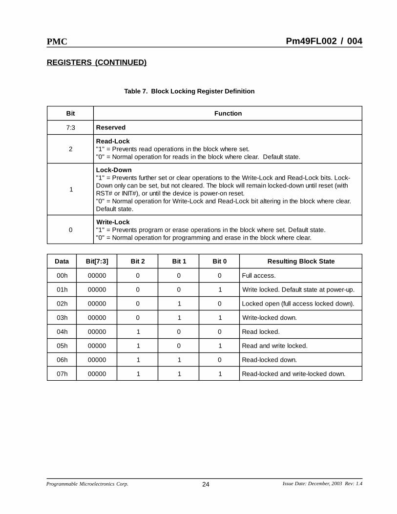
SOFTWARE PRODUCT IDENTIFICATION EXIT
Load Data AAhto
Address 5555h
Load Data 55hto
Address 2AAAh
Load Data 90hto
Address 5555h
Enter ProductIdentif ication
Mode (1,2)
Load Data AAhto
Address 5555h
Load Data 55hto
Address 2AAAh
Load Data F0hto
Address 5555h
Exit ProductIdentif ication
Mode (3)
Load Data F0hto
Address XXXXh
Exit ProductIdentif ication
Mode (3)
or
Chart 3. Software Product Identification Entry/Exit Flowchart
SOFTWARE PRODUCT IDENTIFICATION ENTRY
DEVICE OPERATIONS FLOWCHARTS (CONTINUED)
Notes:1. After entering Product Identification Mode, the Manufacturer ID and the Device ID of Pm49FL00x can be read.
2. Product Identification Exit command is required to end the Product Identification mode and return to standby mode.
3. Either Product Identification Exit command can be used, the device returns to standby mode.

Programmable Microelectronics Corp. Issue Date: December, 2003 Rev: 1.4
PMC Pm49FL002 / 004
34
saiBrednUerutarepmeT 55- o 521+otC oC
erutarepmeTegarotS 56- o 051+otC oC
erutarepmeTgniredloSdaeLtnuoMecafruSegakcaPdradnatS 042 o sdnoceS3C
egakcaPeerf-daeL 062 o sdnoceS3C
sniPllAnodnuorGottcepseRhtiwegatloVtupnI )2( VotV5.0- CC V5.0+
dnuorGottcepseRhtiwegatloVtuptuOllA VotV5.0- CC V5.0+
V CC)2( V0.6+otV5.0-
DC AND AC OPERATING RANGE
rebmuNtraP 200LF94mP 400LF94mP
erutarepmeTgnitarepO 0o 07otC oC 0o 07otC oC
ylppuSrewoPccV V6.3-V0.3 V6.3-V0.3
ABSOLUTE MAXIMUM RATINGS (1)
Notes:1. Stresses under those listed in “Absolute Maximum Ratings” may cause permanent
damage to the device. This is a stress rating only. The functional operation of the deviceor any other conditions under those indicated in the operational sections of this specifica-tion is not implied. Exposure to absolute maximum rating condition for extended periodsmay affected device reliability.
2. Maximum DC voltage on input or I/O pins are +6.25 V. During voltage transitioning period,input or I/O pins may overshoot to VCC + 2.0 V for a period of time up to 20 ns. MinimumDC voltage on input or I/O pins are -0.5 V. During voltage transitioning period, input or I/Opins may undershoot GND to -2.0 V for a period of time up to 20 ns.

Programmable Microelectronics Corp. Issue Date: December, 2003 Rev: 1.4
PMC Pm49FL002 / 004
35
DC CHARACTERISTICS
lobmyS retemaraP noitidnoC niM pyT xaM stinU
IIroftnerruCegakaeLtupnI
snip]0:3[DI,CIV NI VotV0= CC V, CC V= xamCC 001 Aµ
I IL tnerruCegakaeLtupnI V NI VotV0= CC V, CC V= xamCC 1± Aµ
I OL tnerruCegakaeLtuptuO V O/I VotV0= CC V, CC V= xamCC 1± Aµ
I BSVybdnatS CC tnerruC
)edoMCPL/HWF(V=#EMARFLro4HWF HI ,
;zHM33=f V CC V= xamCC005 Aµ
I YRVedoMydaeR CC tnerruC
)edoMCPL/HWF(
V=#EMARFLro4HWF LI ,I;zHM33=f TUO ,Am0=
V CC V= xamCC
01 Am
I 1CCV CC tnerruCdaeRevitcA
)edoMCPL/HWF(
V=#EMARFLro4HWF LI ,I;zHM33=f TUO ,Am0=
V CC V= xamCC
2 51 Am
I 2CC)1( V CC tnerruCesarE/margorP 7 02 Am
V LI egatloVwoLtupnI 5.0- V3.0 CC V
V HI egatloVhgiHtupnI V7.0 CC V CC 5.0+ V
V LO egatloVwoLtuptuO I LO V,Am0.2= CC V= nimCC V1.0 CC V
V HO egatloVhgiHtuptuO I HO 001-= µ V,A CC V= nimCC V9.0 CC V
Note: 1. Characterized but not 100% tested.
AC CHARACTERISTICS
PIN IMPEDANCE (VCC
= 3.3 V, f = 1 MHz, T = 25°C )
pyT xaM stinU snoitidnoC
C O/I)1( ecnaticapaCniPO/I 21 Fp V O/I V0=
C NI)1( ecnaticapaCtupnI 21 Fp V NI V0=
L NIP)2( ecnatcudnIniP 02 Hn
Notes:1. These parameters are characterized but not 100% tested.2. Refer to PCI specification.

Programmable Microelectronics Corp. Issue Date: December, 2003 Rev: 1.4
PMC Pm49FL002 / 004
36
AC CHARACTERISTICS (CONTINUED)
FWH/LPC INTERFACE AC INPUT/OUTPUT CHARACTERISTICS
lobmyS retemaraP noitidnoC niM xaM stinU
I HO )CA(tnerrucgnihctiwS
hgih
V<0 TUO < V3.0 CC V21- CC Am
V3.0 CC V< TUO V9.0< CC V(1.71- CC V- TUO ) Am
V7.0 CC V< TUO V< CC CnoitauqE )1(
)tnioptseT( V TUO V7.0= CC V23- CC Am
I LO )CA( woltnerrucgnihctiwS
V CC V> TUO > V6.0 CC V61 CC Am
V6.0 CC V> TUO V1.0> CC V(1.71- CC V- TUO ) Am
V81.0 CC V> TUO 0> DnoitauqE )1(
)tnioptseT( V TUO V81.0= CC V83 CC Am
I LC tnerrucpmalcwoL V<3- NI < 1- V(+52- NI 510.0/)1+ Am
I HC tnerrucpmalchgiH V CC V>4+ NI > V CC 1+V(+52 NI V- CC /)1-
510.0Am
rwels )2( etarwelsesirtuptuO V2.0 CC V6.0- CC daol 1 4 sn/V
fwels )2( etarwelsllaftuptuO V6.0 CC V2.0- CC daol 1 4 sn/V
Notes:1. See PCI specification.2. PCI specification output load is used.
FWH/LPC INTERFACE CLOCK CHARACTERISTICS
lobmyS retemaraP niM xaM stinU
t CYC emiTelcyCkcolC 03 sn
t HGIH emiThgiHkcolC 11 sn
t WOL emiTwoLkcolC 11 sn
etaRwelSkcolC 1 4 sn/V
etaRwelS#TSRro#TINI 05 sn/Vm

Programmable Microelectronics Corp. Issue Date: December, 2003 Rev: 1.4
PMC Pm49FL002 / 004
37
AC CHARACTERISTICS (CONTINUED)
lobmyS retemaraP niM xaM stinU
T CYC emiTelcyCkcolC 03 sn
T US emiTpUteStupnI 7 sn
TH emiTdloHtupnI 0 sn
T LAV tuOataDotkcolC 2 11 sn
T NO )yaledevitcaottaolf(emiTevitcAotkcolC 2 sn
T FFO )yaledtaolfotevitca(emiTevitcanIotkcolC 82 sn
FWH/LPC MEMORY READ/WRITE OPERATIONS CHARACTERISTICS
tL O W
tHIGH
tCYC
0.5 V CC
0.4 V CC
0.3 V CC
0.4 V C C p-to-p(minimum)
0.6 V CC
0.2 V CC
FWH/LPC INTERFACE CLOCK WAVEFORM
FWH/LPC INTERFACE MEASUREMENT CONDITION PARAMETERS
lobmyS eulaV stinU
V HT1 V6.0 CC V
V LT1 V2.0 CC V
V TSET V4.0 CC V
V XAM1 V4.0 CC V
etaRegdElangiStupnI sn/V1
Note: 1. The input test environment is done with 0.1 VCC of overdrive over VIH and VIL. Timing parameters mustbe met with no more overdrive that this. VMAX specifies the maximum peak-to-peak waveform allowedfor measuring input timing. Production testing may use different voltage values, but must correlateresults back to these parameter.

Programmable Microelectronics Corp. Issue Date: December, 2003 Rev: 1.4
PMC Pm49FL002 / 004
38
AC CHARACTERISTICS (CONTINUED)
V T E S T
V TL
V T H
tVAL
tO F F
tO N
CLK
FWH[3:0] orLAD[3:0]
(Val id Output Data)
FWH[3:0] orLAD[3:0]
(Float Output Data)
FWH/LPC OUTPUT TIMING PARAMETERS
tHtSU
INPUT VALID
V T H
V TL
V TEST
V M A X
FWH[3:0] orLAD[3:0]
(Valid Input Data)
CLK
FWH/LPC INPUT TIMING PARAMETERS

Programmable Microelectronics Corp. Issue Date: December, 2003 Rev: 1.4
PMC Pm49FL002 / 004
39
T P R S T
T K R S T
T R S T PT R S T
T RSTF
V C C
CLK
RST#/INIT#
FWH[3:0] orLAD[3:0]
FWH4 orLFRAME#
FWH/LPC RESET AC WAVEFORMS
lobmyS retemaraP niM xaM stinU
T TSRP VotemiTevitcAteseR CC elbatS 1 sm
T TSRK otemiTevitcAteseR kcolC elbatS 001 sµ
T PTSR htdiWesluPteseR 001 sn
T FTSR yaleDtaolFtuptuOotevitcAteseR 05 sn
T TSR)1( evitcAtupnIotemiTevitcanIteseR 1 sµ
FWH/LPC RESET OPERATION CHARACTERISTICS
AC CHARACTERISTICS (CONTINUED)
A/A MUX MODE TEST LOAD CONDITION
TO TESTER
30 pFC L
TO DUT
A/A MUX MODE INPUT TEST MEASUREMENT CONDITION PARAMETERS
3.0 V
0.0 V
1.5 VA CMeasurementLevel
Input
Note: 1. There will be a 10 µs reset latency if a reset procedure is performed during a programming or eraseoperation.

Programmable Microelectronics Corp. Issue Date: December, 2003 Rev: 1.4
PMC Pm49FL002 / 004
40
AC CHARACTERISTICS (CONTINUED)
A/A MUX MODE READ OPERATIONS CHARACTERISTICS
lobmyS retemaraP niM xaM stinU
t CR emiTelcyCdaeR 072 sn
t CCA yaleDtuptuOotsserddA 021 sn
t TSR emiTpu-teSsserddAwoRothgiH#TSR 1 sm
t SA emiTpu-teSsserddA#C/R 54 sn
t HA emiTdloHsserddA#C/R 54 sn
t EO yaleDtuptuOot#EO 05 sn
t FD ZhgiHtuptuOot#EO 0 03 sn
t HO tsrifderuccorevehcihw,sserddAro#EOmorfdloHtuptuO 0 sn
t SCV V CC emiTpu-teS 05 sµ
A/A MUX MODE READ OPERATIONS AC WAVEFORMS
R O W A D D R E S S
tRC
tACC
tO E tDF
tO H
O U T P U TVALID
HIGH Z
A D D R E S S
O E #
W E #
OUTPUT
V C C
tVCS
RST#
tRST
COLUMN ADDRESS
tAS tAH tAS tAH
R/C#

Programmable Microelectronics Corp. Issue Date: December, 2003 Rev: 1.4
PMC Pm49FL002 / 004
41
A/A MUX MODE WRITE OPERATIONS AC WAVEFORMS
R O W A D D R E S S
tRC
tC W H tOEH
tDS tDH
INPUTD A T A
HIGH Z
A D D R E S S
O E #
W E #
OUTPUT
V C C
tVCS
RST#tRST
COLUMN ADDRESS
tAS tAH tAS tAH
R/C#
tOES
AC CHARACTERISTICS (CONTINUED)
A/A MUX MODE WRITE (PROGRAM/ERASE) OPERATIONS CHARACTERISTICS
lobmyS retemaraP niM xaM stinU
t TSR emiTpu-teSsserddAwoRothgiH#TSR 1 sm
t SA emiTpu-teSsserddA#C/R 05 sn
t HA emiTdloHsserddA#C/R 05 sn
t HWC emiThgiH#EWot#C/R 05 sn
t SEO emiTpu-teShgiH#EO 02 sn
t HEO emiTdloHhgiH#EO 02 sn
t SD emiTpu-teSataD 05 sn
t HD emiTdloHataD 5 sn
t PW htdiWesluPetirW 001 sn
t HPW hgiHhtdiWesluPetirW 001 sn
t PB emiTgnimmargorPetyB 04 sµ
t CE emiTelcyCesarEkcolBrorotceS,pihC 08 sm
t SCV V CC emiTpu-teS 05 sµ

Programmable Microelectronics Corp. Issue Date: December, 2003 Rev: 1.4
PMC Pm49FL002 / 004
42
A/A MUX MODE BYTE PROGRAM OPERATIONS AC WAVEFORMS
A/A MUX MODE CHIP ERASE OPERATIONS AC WAVEFORMS
tW P tW P H tEC
A A 55DATA IN
A D D R E S S
O E #
W E #
R/C#
6-Byte Chip Erase Command
tDHtDS
tC W H
5555 55552AAA 5555 55552AAA
A A 5580 10
AC CHARACTERISTICS (CONTINUED)
tW P
tW P H tBP
5555 5555 BYTE ADDRESS2AAA
A A 55 A0 INPUTD A T A
VALIDD A T A
DATA
A D D R E S S
O E #
W E #
R/C#
4-Byte Program Command
tDHtDS
tC W H

Programmable Microelectronics Corp. Issue Date: December, 2003 Rev: 1.4
PMC Pm49FL002 / 004
43
A/A MUX MODE SECTOR/BLOCK ERASE OPERATIONS AC WAVEFORMS
tW P tW P H tEC
A A 55DATA IN
A D D R E S S
O E #
W E #
R/C#
6-Byte Block Erase Command
tDHtDS
tC W H
5555 55552AAA 5555 S E C T O R O RB L O C K A D D R E S S
2AAA
A A 5580 30/50
A/A MUX MODE TOGGLE BIT AC WAVEFORMS
tOEH
W E #
R/C#
O E #
I/O6
tO E
DD
A D D R E S S R O W C O L U M N
Note: 1. Toggling OE# will operate Toggle Bit.2. I/O6 may start and end from “1” or “0” in random.
AC CHARACTERISTICS (CONTINUED)

Programmable Microelectronics Corp. Issue Date: December, 2003 Rev: 1.4
PMC Pm49FL002 / 004
44
A/A MUX MODE DATA# POLLING AC WAVEFORMS
tOEH
W E #
R/C#
O E #
I/O7
tO E
DD
A D D R E S S R O W C O L U M N
D#D#D#
Note: Toggling OE# will operate Data# Polling.
AC CHARACTERISTICS (CONTINUED)
retemaraP tinU pyT xaM skrameR
emiTesarEkcolB/rotceS sm 05 08 noitelpmocesareotdnammocesaregnitirwmorF
emiTesarEpihC sm 05 08 noitelpmocesareotdnammocesaregnitirwmorF
emiTgnimmargorPetyB µs 52 04dnammocmargorpelcyc-ruoffoemitehtsedulcxE
noitucexe
PROGRAM/ERASE PERFORMANCE
Note: These parameters are characterized but not 100% tested.
RELIABILITY CHARACTERISTICS (1)
retemaraP niM pyT tinU dohteMtseT
ecnarudnE 000,001 )2( selcyC 711AdradnatSCEDEJ
noitneteRataD 02 sraeY 301AdradnatSCEDEJ
ledoMydoBnamuH-DSE 000,2 000,4> stloV 411AdradnatSCEDEJ
ledoMenihcaM-DSE 002 004> stloV 511AdradnatSCEDEJ
pU-hctaL I+001 1CC Am 87dradnatSCEDEJ
Notes: 1. These parameters are characterized but not 100% tested.2. Preliminary specification only and will be formalized after cycling qualification test.

Programmable Microelectronics Corp. Issue Date: December, 2003 Rev: 1.4
PMC Pm49FL002 / 004
45
PACKAGE TYPE INFORMATION
TOP VIEW SIDE VIEW
32V32-Pin Thin Small Outline Package (VSOP - 8 mm x 14 mm)( measure in millimeters)
0.50B S C
1.050.95
0.270.17
0.150.05
Pin 1 I.D.
12.5012.3014.2013.80
8.107.90
1.20M A X
0.250°5°
0.20
0.10
0.700.50
32J32-Pin Plastic Leaded Chip Carrier (measured in millimeters)
Pin 1 I.D.
15.1114.86
14.0513.89
1.27 Typ.0.810.66
11.5111.35
12.5712.32
0.74X30°
13.4612.45
0.530.33
2.411.93
3.563.18
SEATINGPLANE

Programmable Microelectronics Corp. Issue Date: December, 2003 Rev: 1.4
PMC Pm49FL002 / 004
46
REVISION HISTORY
etaD .oNnoisiveR segnahCfonoitpircseD .oNegaP
2002,enuJ 0.1 noitacilbupyranimilerP llA
2002,yluJ 1.1 noitacilbuplamroF llA
3002,yraunaJ 2.1
noitacificepsemitesarednamargorpdesiveR 44,14,1
gnikcoLkcolBrofrebmuntrapehtnoopytdetcerroCretsigeR
32
3002,rebmevoN 3.1
noitamrofni800LF94mPdevomeR llA
epytegakcaproftnemerusaemhcnidevomeRnoitamrofni
54
3002,rebmeceD 4.1
eerf-daelrofnoitamrofnigniredrotcudorpdegnahCnoitpoegakcap
43,4,1
morfselcycesare/margorpdeetnarugdedargpU)yranimilerp(000,001ot000,05
44,1